Fabrication of aluminium nanostructures for...
18
This content has been downloaded from IOPscience. Please scroll down to see the full text. Download details: IP Address: 193.49.161.184 This content was downloaded on 04/02/2016 at 09:06 Please note that terms and conditions apply. Fabrication of aluminium nanostructures for plasmonics View the table of contents for this issue, or go to the journal homepage for more 2015 J. Phys. D: Appl. Phys. 48 184002 (http://iopscience.iop.org/0022-3727/48/18/184002) Home Search Collections Journals About Contact us My IOPscience
Transcript of Fabrication of aluminium nanostructures for...

This content has been downloaded from IOPscience. Please scroll down to see the full text.
Download details:
IP Address: 193.49.161.184
This content was downloaded on 04/02/2016 at 09:06
Please note that terms and conditions apply.
Fabrication of aluminium nanostructures for plasmonics
View the table of contents for this issue, or go to the journal homepage for more
2015 J. Phys. D: Appl. Phys. 48 184002
(http://iopscience.iop.org/0022-3727/48/18/184002)
Home Search Collections Journals About Contact us My IOPscience
1 © 2015 IOP Publishing Ltd Printed in the UK
1. Introduction
When excited at an adequate energy, metallic nanostructures support localized surface plasmon resonances (LSPRs) due to the coherent, collective oscillation of their surface conduction electrons [1]. Due to LSPRs, the electromagnetic (EM) field is strongly enhanced and locally confined in the vicinity of a metallic nanostructure, which intensively absorbs and scatters light. The fundamental properties of LSPRs, energy and line-width (or Full Width at Half Maximum, FWHM), depend on the intrinsic properties of the metal (electronic band structure, dielectric function), its geometry, and the refractive index of the surrounding medium. Accordingly, metallic nanostruc-tures exhibit extremely interesting optical properties leading to various applications such as metal-enhanced fluorescence
[2], ultra-sensitive sensing [3] and surface enhanced Raman spectroscopy (SERS) [4], to name only a few. For several decades plasmonics have been almost exclusively studied in the visible and near-infrared portion of the electromagnetic (EM) spectrum by using nanostructures made of gold or silver. However, these noble metals have inherent limitations hindering the development of plasmonic devices towards the blue and ultraviolet (UV) parts of the EM spectrum. Gold does not exhibit plasmonic resonances at wavelengths shorter than 520 nm due to its interband transitions. Silver nanostruc-tures exhibit LSPRs down to 350 nm but suffer from strong oxidation and lose their plasmonic properties over time. To overcome those issues, aluminium (or AL) plasmonics is now emerging. Due to its intrinsic properties, such as its high plasma energy of 15.6 eV, aluminium behaves like a metal
Journal of Physics D: Applied Physics
Fabrication of aluminium nanostructures for plasmonics
Jérôme Martin and Jérôme Plain
Institut Charles Delaunay, LNIO, Université de Technologie de Troyes, CNRS UMR 6281, Troyes, France
E-mail: [email protected] and [email protected]
Received 15 August 2014, revised 24 October 2014Accepted for publication 10 November 2014Published 15 December 2014
AbstractMetallic nanostructures are the building blocks for nanoplasmonics and for subsequent applications in nanooptics. For several decades, plasmonics have been almost exclusively studied in the visible region by using nanostructures made of noble metals exhibiting plasmonic properties in the near infrared to visible range. This notwithstanding, emerging applications will require the extension of nanoplasmonics toward higher energies, particularly in the UV range. Therefore, alternative metals, often described as poor metals are emerging to achieve that goal. Among all these metals, aluminium appears to be one of the most appealing for extending plasmonics towards ultraviolet energies. Aluminium is cheap, widely available, compatible with optoelectronic devices and exhibits plasmonic properties over a wide range of energies, from the infrared to the deep UV. Our aim is to present a review of current research centred on the fabrication of aluminium nanostructures. Mastering the geometry of aluminium nanostructures is extremely important in order to tune their plasmonic properties and target a given application. First we give an introduction to the nanofabrication of aluminium nanostructures within the context of plasmonics. The review then focuses on the possible geometries that such structures may take when fabricated with specific fabrication techniques. Each technique is detailed and the plasmonic properties of the aluminium nanostructures are briefly described. When possible, an example of an application is given. Finally, the future applications of aluminium plasmonics are highlighted and a conclusion with perspectives is given.
Keywords: aluminium, plasmonics, nanofabrication
(Some figures may appear in colour only in the online journal)
J Martin and J Plain
Fabrication of aluminium nanostructures for plasmonics
Printed in the UK
184002
JPhysd
© 2015 IOP Publishing Ltd
2015
48
J. Phys. d: Appl. Phys.
JPd
0022-3727
10.1088/0022-3727/48/18/184002
Paper
18
Journal of Physics d: Applied Physics
MMd
0022-3727/15/184002+17$33.00
doi:10.1088/0022-3727/48/18/184002J. Phys. D: Appl. Phys. 48 (2015) 184002 (17pp)
J Martin and J Plain
2
up to energies located in the deep UV, while keeping rela-tively low losses, except within a relatively narrow energy range centred at 1.5 eV where interband transitions are active [5]. Although plasmonic resonances in aluminium nanostruc-tures have been observed since the early eighties [6] thanks to electron energy loss spectroscopy (EELS), aluminium plas-monics has truly begun in recent years [7–16]. In contrast to noble metals, aluminium is cheap and widely available as it is a very abundant material on Earth. This is a tremendous advantage for industry related applications which could have a strong impact in terms of economic benefits. For instance, aluminium is compatible with optoelectronic devices and CMOS technology. Therefore, aluminium opens avenues for plasmonic engineering of the optical properties of wide bandgap semiconductors such as ZnO [17] or GaN related alloys [18], which could create a new market in the field of optoelectronics. On a broader level, aluminium plasmonics is very appealing for a lot of applications: surface enhanced Raman spectroscopy in ultraviolet [19, 20], metal enhanced fluorescence [21], label-Free biosensing applications [22], non-linear plasmonics [23], light harvesting devices [24], photodetection [25], photocatalysis [26] or high data density storage [27]. Nevertheless, studies of LSPRs in the UV region have been sporadically reported, implying that aluminium for plasmonics is still in its infancy. Of paramount importance in the development of future aluminium plasmonic applica-tions is the capability to fabricate well defined aluminium nanostructures in order to fine-tune their plasmonic proper-ties. This article aims to give an overview of current research centred on the fabrication (and to a lesser extent, the optical properties) of aluminium nanostructures. The review mainly focuses on the feasible geometries that such nanostructures may take when fabricated with specific methods. Each method is therefore described and the plasmonic properties of the fab-ricated aluminium nanostructures are briefly described. More precise information concerning the plasmonic properties of
aluminium nanostructures is available in [28], which is pub-lished in the same issue. Finally, the potential applications of aluminium plasmonics are highlighted and a conclusion with perspectives is given.
2. Lithography
This review devotes a first and large section to the different types of lithographic methods used for the fabrication of alu-minium nanostructures. Indeed, in order to investigate their optical properties as a function of features like their size, shape, height, or dielectric environment (substrate, encapsu-lating layers), lithography appears as an obvious choice, as it allows for a precise control of the nanostructure’s geometry.
2.1. Electron beam lithography
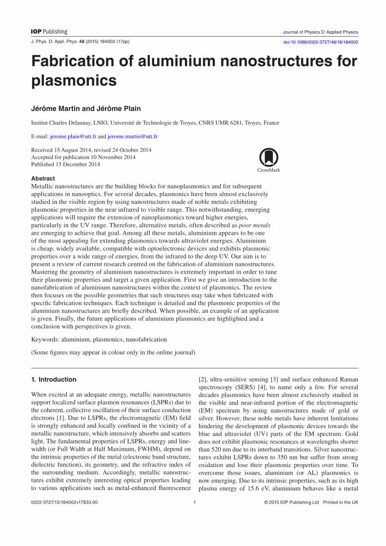
Electron beam lithography (EBL) is a very efficient tool for the fabrication of plasmonic nanostructures [29]. The main steps involved in EBL are described in figure 1. The first step consists of exposing a positive resist (spin coated on a sub-strate beforehand) using a scanning electron beam, allowing one to write down the desired pattern shape in the resist. The electrons interact with the resist breaking its polymeric chains as illustrated by the inset in figure 1(a). The resist is then developed in a selective solvent as the exposed areas contain smaller chains with higher solubility compared to non-exposed areas. Then the entire sample is metallized using for instance, evaporation techniques. Before the evapora-tion of the metal, it is important to get an inverted profile in the resist as shown in figure 1(b). Indeed, the discontinuity between the metal deposited onto the substrate and the resist (figure 1(c)) is mandatory for the final step of resist removal, or lift-off (figure 1(d)). Moreover, a minimum ratio of 1 : 3 for the metal:resist thickness is used to prevent any contact. In
Figure 1. Main steps of EBL for the deposition of metallic nanostructures. (a) Electron-beam (red colour) exposure of the resist (orange colour) leading to polymeric chain breaking (inset). (b) Inverted resist profile after development. The profile shape is due to overexposure at the resist:substrate interface. (c) Metal coating (grey colour) and (d) the remaining metallic nanostructures after the stripping of the resist in a solvent. Inspired by [29].
J. Phys. D: Appl. Phys. 48 (2015) 184002
J Martin and J Plain
3
the last step, the sample is dipped in a solvent dissolving the remaining resist and lifting up the unwanted metallic areas.
At this point, it should be specified that aluminium can be evaporated by using either electron-beam or thermal evapora-tion, with a typical deposition rate between 0.1 nm s−1 and 0.2 nm s−1 and a base pressure between 10−6 and 10−7 Torr. These experimental conditions are of importance in order to keep a relatively smooth surface. However, there is a difficulty inherent in the evaporation of aluminium due to its tendency to nucleate in the early stage of growth. This prevents a very smooth surface of the Al nanostructures, which exhibit large grain size leading to distorted shapes. These features are more or less visible on the SEM (scanning electron microscopy) images of lithographed aluminium nanostructures presented in this review.
The goal here is to give a relevant list of studies involving EBL for the fabrication of aluminium nanostructures. EBL has proven to be a very efficient tool for the fabrication of alu-minium nanostructures aiming at the rigorous study of their plasmonic properties. Indeed, the size and shape of metallic nanostructures are easily tunable when fabricated by EBL, with dimensions ranging from a few tens of nm to some μm. Such full parametric studies are very interesting in order to investigate the fundamental properties of aluminium plas-mons such as their energy dispersion relation or their extinc-tion, absorption and scattering efficiencies.
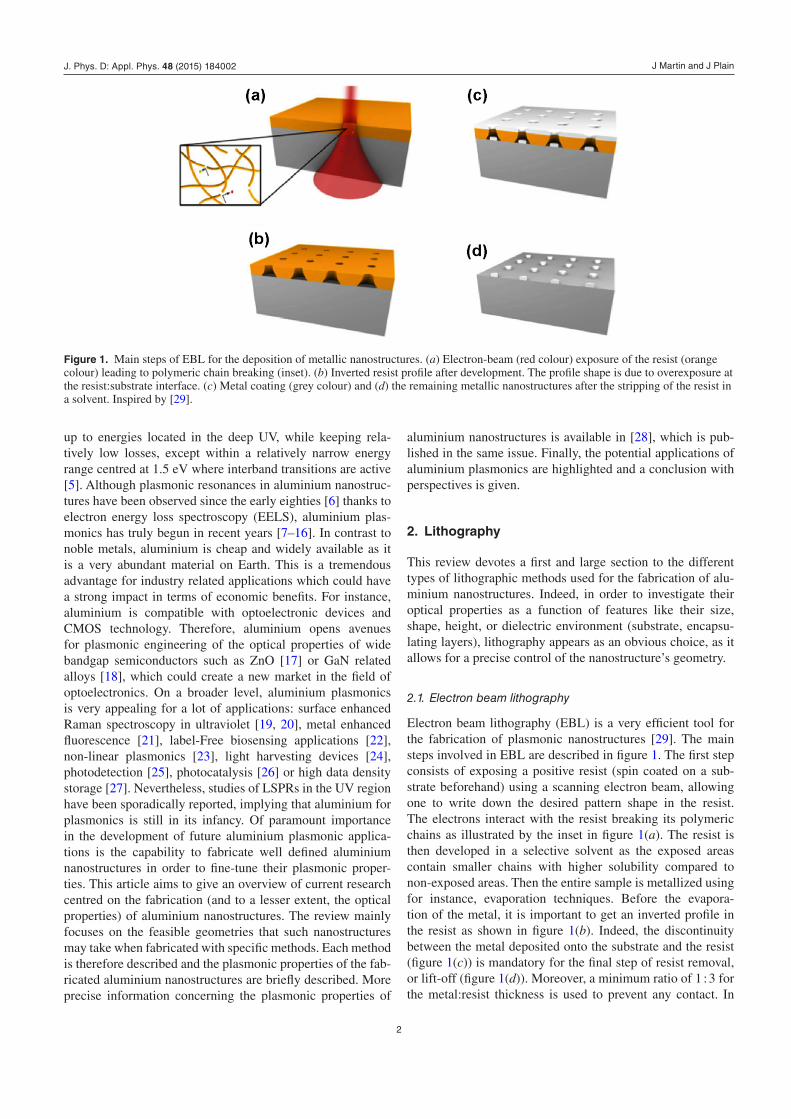
Let us begin with a recent example where the plasmonic properties of simple structures consisting of aluminium nano-disks are studied by Knight et al [14]. The Al nanodisks fab-ricated by EBL are shown in figure 2(b). Individual scattering spectra have been measured and theoretically calculated on each Al nanodisk as is visible in the graphs in figures 2(a) and (c). Obviously, the radiative properties of LSPRs sus-tained by the Al nanodisks range from the visible to ultraviolet wavelengths. The main peak visible in the ultraviolet (for the smallest nanoparticle) is the signature of typical Lorentzian dipolar plasmonic resonance. When the diameter of the nan-oparticle increases, the LSPR is red-shifted and becomes broader. This effect is due to phase delay across the nanopar-ticles decreasing the lifetime (or increasing the linewidth) of the plasmonic resonances [30]. Due to phase delay, additional peaks with lower wavelengths and lower relative intensities appear in the dark field spectra. These peaks actually corre-spond to the signature of high order plasmonic resonances (quadrupolar resonance, for instance) sustained by larger Al nanodisks. In this study they particularly pointed out that the aluminium plasmonic resonances are remarkably sensi-tive to the presence of the native oxide ((Al2O3) or alumina) within the metal. The percentage of alumina in the nanodisks is retrieved by comparing the experimental resonances with the resonances calculated by numerical simulations where the amount of alumina is taken into account in the dielectric func-tion. At this point, it is important to remember that aluminium does not oxidise in depth but passivates with a stable alumina shell, roughly equal to 3 nm [7], keeping Al plasmonic prop-erties over time even for nanostructures with surfaces exhib-iting relatively large grain size. For instance, the evolution of the plasmonic properties of aluminium surfaces during their
oxidation is investigated in [31] while the mechanisms of alu-minium nanoparticle oxidation are investigated in [32].
In an earlier study, Knight et al also thoroughly studied the radiative properties of individual Al nanoantennas (or nanorods) made by EBL thanks to spatial resolved cathodo-luminescence [11]. Plasmonic resonances sustained by EBL-made aluminium nanodisks have also been investigated by Zorić et al [30]. They wrote down a specific pattern shape in the resist leading to large area and two-dimensional pat-terns of randomly distributed nanodisks with well-defined size and shape, narrow size distribution and tunable interpar-ticle distance. Thanks to the characterization of these samples by extinction spectroscopy and theoretical calculations, they studied the radiative and non-radiative damping mechanisms of dipolar plasmonic resonances sustained by Al (and also gold and platinum) nanodisks, and linked the results to the specific electronic band structure of the considered metal. Note that the same group thoroughly investigated the plasmonic proper-ties of Al nanodisks earlier (2008), but the method of fabrica-tion was different (hole-mask colloidal lithography, or HCL) [7], and this work will be discussed later.
Lecarme et al have recently worked on Al nanostructures made by EBL [15]. This study focused on the plasmonic prop-erties of Al nanorods in the infrared to visible region of the EM spectrum. Here the structures consist of nanorods with varying dimensions as shown in figures 3(b) and (c). The spectra (figure 3(a)) correspond to extinction measurements
Figure 2. (a) Experimental darkfield spectra of individual nanodisks with diameters ranging from 70–180 nm. (b) SEM micrographs of the corresponding nanodisk structures. (Scale bar 100 nm). (c) FDTD simulations of the nanodisk spectra, assuming a 3 nm surface oxide and a SiO2 substrate. Reprinted with permission from [14]. Copyright 2014 American Chemical Society.
J. Phys. D: Appl. Phys. 48 (2015) 184002

J Martin and J Plain
4
under unpolarized illumination of ordered arrays of 20 nm thick Al nanorods with a constant aspect ratio (length divided by width) of 2. Both the longitudinal (L) and transversal (T) plasmonic modes sustained by the nanorods are naturally red-shifted when the dimensions of the rod are increased. Interestingly, an additional feature around 800 nm appears on the spectra for all the nanorods. Indeed, a more or less vis-ible third peak appears between the L and the T mode peaks. This feature is clearly visible for the smaller nanorod (black curve) and actually results from coupling between the LSPR and the energy-localized IT of Al. This coupling can be adjusted thanks to EBL parameters (as the plasmonic reso-nance depends on the geometry of the nanorod), and used to switch from highly scattering particle arrays to absorbing particle arrays as is shown quite nicely in the article. A large number of other parameters have been varied in this work. For instance, the influence of the distance between each nanorod on their optical properties has also been studied. Indeed, in a two-dimensional lattice, the usual choice for EBL fabrication,
the nearest-neighbour interactions have to be taken into account to fully understand the optical properties of metallic nanoparticle arrays. This study demonstrates again that EBL-made samples make possible the thorough study of precise mechanisms such as IT-plasmon interactions in aluminium nanostructures.
Another complete parametric study involving EBL can be retrieved in [33] where arrays of Al and gold (Au) nanorods are fabricated. By combining their experimental results with discrete dipole approximation calculations, the optical prop-erties of Au plasmonic structures are compared with similar Al structures, and solar cell light-trapping applications are discussed. It is shown that Al nanoparticles are interesting for amorphous silicon solar cells, but their application for polycrystalline solar cells is limited by the presence of the IT mentioned above. In [34], EBL was used to fabricate alu-minium nanoantennas with various aspect ratios and their plasmonic properties have been studied by EELS. In this work, the multipolar plasmonic resonances sustained by the nanoantennas have been mapped at the nanometer scale and their damping mechanisms have been studied. More particu-larly, it is shown that in the blue-UV spectral range, high order plasmonic modes present a quality factor roughly two times higher than low order plasmonic modes at the same energy. EBL has also been used to fabricate aluminium nanohole arrays [22]. In contrast to all the above mentioned references, here the aluminium film is deposited before the EBL sensitive resist. After the electronic exposure of the resist and the devel-opment of the nanoholes, the aluminium layer is selectively etched using a well-adjusted inductively coupled plasma (ICP) chemical dry etching process. After the resist lift-off, this process leads to well defined aluminium nanohole arrays over a large area. These Al nanostructures are then proven to be efficient for biosensing.
A very nice example of an application exploiting the plas-monic properties of EBL made aluminium nanostructures is the colour generation for printing applications [35]. As alu-minium is a low cost material and exhibits plasmonic proper-ties from the infrared to the ultraviolet when nanostructured, high-resolution plasmonic colour printing appears as a direct industry-related application, such as security tagging, cryp-tography, and information storage. Here, EBL has been used in order to fabricate plasmonic nano-pillars with varying diameters on a silicon substrate. The nano-pillars are made of negative-tone resist (which is patterned during the electronic irradiation and the subsequent development), subsequently capped with aluminium, resulting in the plasmonic nano-pil-lars. Then, matrices of pixels are designed, each pixel con-sisting of four plasmonic nanopillars. By varying the size of the nanopillars and the distance between them in each pixel, they were able to reproduce all the colour and tone variations of a reproduction of Monet’s Impression, Sunrise, as is nicely demonstrated in the article.
A second example of structural colouration using alu-minium nanostructures can be found in [36]. Without going into detail, the nanostructures consist of coupled aluminium nanodisks and nanoholes. Here the hybridization between LSPR modes in the nanodisks and nanoholes is used to design
Figure 3. (a) Experimental extinction spectra of size-variable Al nanorods with the aspect ratio l/w maintained at 2. (b) SEM micrograph of a thin Al nanorod array on KTaO3. Scale bar: 200 nm. (c) Schematic view of the geometry of the structures. Reprinted with permission from [15]. Copyright 2014 American Chemical Society.
J. Phys. D: Appl. Phys. 48 (2015) 184002

J Martin and J Plain
5
and fabricate bright angle-insensitive colours tunable across the entire visible spectrum. This method has tremendous potential for large scale implementation of structural colours in plastic products for daily use, as explicitly stated in the corresponding article. As a final example, Al nanorod arrays made by EBL have also been used by Olson et al for the fab-rication of plasmonic pixels [37]. In this study, the plasmonic properties of the pixels are intensively investigated and are proved to be very appealing for future display technologies.
2.2. Colloidal lithography
Colloidal lithography (CL), also known as nanosphere lithog-raphy (NSL) is based on the self-organization of colloidal particles (for instance polystyrene beads) on surfaces to form 2D or 3D evaporation (or etch) masks [38]. This method is cheaper than EBL and less demanding in terms of facilities. A well-known version of NSL is the use of organized 2D col-loidal crystals with a hexagonal close-packed pattern as an evaporation mask, often in combination with reactive ion etching. The subsequent evaporation through the mask defines the resulting metallic pattern, and the material deposition con-ditions such as the evaporation angle or specific deposition technique (electron beam deposition, sputtering, epitaxial growth, thermal deposition) enable the variation of the final pattern. A very simple schematic illustrating NSL (here for the fabrication of silver nanotriangles) is visible in figure 4 from [39].
The critical step in CL is to form a well organized 2D col-loidal layer with as few defects as possible (such as disloca-tions in the colloidal crystal, or vacancies). The formation of the colloidal crystal can be achieved by arranging the col-loids contained in commercial solutions onto the substrate. To achieve that end, several methods are commonly used [40]: drop-coating, spin-coating, dip-coating, electropho-retic deposition, or self-assembly at the gas–liquid interface. A surfactant can be added to the solution to assist the col-loids in wetting the substrate, or functionalized colloids are purchasable to avoid aggregates and to form a homogeneous thin layer. The functionalization of the substrate, making it
hydrophilic is also a solution to enhance the wetting of the colloids [10]. Assuming a good and homogeneous wetting between the colloids and the substrate (which has to be highly hydrophilic), the final thickness of the colloid’s layer (e.g. monolayer, bilayer, ...) is tunable by varying the concentra-tion of the colloidal solution and the volume spread onto the substrate. Actually, such methods of coating involve a com-plex dynamic process associated with the evaporation of the colloidal solution (which is time and solvent dependent) and its viscosity gradients. NSL has been used to fabricate alu-minium nanoparticles [9, 26, 41]. An example of NSL leading to aluminium nanotriangles is shown in figure 5, taken from reference [9]. Here the hexagonal 2D pattern of polystyrene beads has been used as the evaporation mask leading to the nanotriangles of aluminium. By varying their width (typically from 95 to 230 nm for a constant 50 nm height), such alu-minium nanotriangles sustain LSPRs tunable from 350 nm to 800 nm as proved by UV-visible extinction measurements and confirmed by theory. In this work, the native alumina shell has been characterized by combining scanning electron microscope and atomic force microscopy. It is demonstrated that the presence of the alumina layer, especially on the tips of the nanotriangles, results in a significant red shift of the LSPR maximum or λmax. By merging the samples in different solvents, it is also experimentally shown that the plasmonic resonances sustained by aluminium nanotriangles have a refractive index sensitivity equal to 0.405 eV per refractive index unit (0.405 eV per RIU). The plasmonic properties of unoxidised triangular nanoparticles of similar size and geom-etry have been calculated showing that the refractive index sensitivity is significantly decreased by the oxide layer.
CL has two inherent limitations. First, the size of the metallic nanostructures are completely determined by the diameter of the colloids used for the mask. One can easily imagine that achieving ultrasmall aluminium structures (in order to tune their plasmonic resonances into the deep UV) would need very small colloids, with diameters typically less than or equal to 200 nm. Such small colloids (as poly-styrene nanospheres available in commerce) are very difficult to deposit and align in well-ordered crystals over large areas.
Figure 4. Schematic illustration of hexagonal compact arrays of microbeads used as an evaporation mask (left panel) and subsequent arrays of silver nanotriangles after the evaporation and the bead’s removal (right panel). The Bead’s diameter is 542 nm and the thickness of Ag (thermally evaporated) is 48 nm. Reprinted with permission from [39]. Copyright 2001 American Chemical Society.
J. Phys. D: Appl. Phys. 48 (2015) 184002

J Martin and J Plain
6
Secondly, as the available diameters of colloids are limited, the continuous tuning of the metallic nanostructures' size (and consequently of their plasmonic properties) is not trivial. In [10], in order to fabricate tunable aluminium nanostructures by NSL, a method is proposed to tune the gap between the polystyrene microbeads (mean diameter 336 nm) with a hex-agonal closely-packed arrangement. To achieve this, the beads are heated under a microwave, resulting in the shrinking of the spaces between them as illustrated in figure 6. The spaces are thus tuned by changing the heating time and the following evaporation step leads to aluminium nanostructures with a typical size tunable from 80 to 50 nm. Note that the shape of the nanostructures gradually changes from triangles to sphe-roids. Finally, the localized plasmonic resonances are tuned from 342 to 270 nm, as illustrated in figure 6. By using dif-ferent bead diameters, this method is therefore very appealing for tuning the plasmonic properties of aluminium nanostruc-tures from the visible to the mid UV.
Another version of CL, called sparse CL (SCL) [42] has also been used for the fabrication of aluminium thin films per-forated with nanoholes [43]. In contrast to NSL, the evapora-tion mask used in SCL is defined by a sparse monolayer of colloidal particles. This method enables the production of large
areas of features like nanoholes in thin films, with sizes down to 20 nm and which occupy 10–50% of the total surface area. In [43], propagating surface plasmon polaritons (SPP), LSPR and interactions between Al IT and LSPR have been thoroughly studied in aluminium (but also in gold) thin films perforated with nanoholes. The last version of CL related here is hole mask CL (HCL), which has been developed by Fredriksson et al and detailed in [44]. The main difference in HCL is the presence of a sacrificial layer combined with a thin film con-taining nanoholes (the hole-mask) used as a mask template during the evaporation (or etch) steps to define the pattern. The hole-mask is removed after processing thanks to the sacrificial layer. HCL has been used by Langhammer et al [7] to fabricate well defined aluminium nanodisks randomly distributed on the substrate combined with relatively large particle–particle separation. Thus, both far and near field optical coupling are avoided (such as Bloch modes or Woods anomaly). Consequently, plasmonic resonances tunable from the infrared to the ultraviolet sustained by HCL-made aluminium nano-disks have been thoroughly studied in this pioneering work in the field of aluminium plasmonics, as illustrated in figure 7.
Let us finish with a NSL-based method proposed in [45] allowing for the fabrication of crescent-shaped aluminium
Figure 5. (a) DDA simulation of the effect of a 2 nm layer of Al2O3 on the LSPR of an Al nanoparticle. The inset shows a side view of the core-shell Al nanoparticle. The total height and width of the nanoparticle was fixed at 50 and 90 nm, respectively. (b) SEM image of 50 nm thick NSL Al nanoparticle arrays on a silicon substrate. Reprinted with permission from [9]. Copyright 2008 American Chemical Society.
Figure 6. SEM images of Al nanostructures fabricated using nanosphere masks heated for (a) 0 s, (b) 90 s, (c) 100 s, and (d) 110 s. The deposition thickness was 30 nm. The scale bar is 300 nm. (e) Normalized extinction spectra from the corresponding nanostructures. Reprinted with permission from [10]. Copyright 2012 American Institute of Physics.
J. Phys. D: Appl. Phys. 48 (2015) 184002

J Martin and J Plain
7
nanoantennas. Even if no samples have been fabricated in this study, the plasmonic properties of such nanocrescents in the UV-VIS region are thoroughly analysed with calculations. Interestingly, higher-order modes sustained by these struc-tures exhibit intense and controllable hot spots suitable for applications in the UV regime, such as SERS.
2.3. Interference lithography
Laser interference lithography (LIL or IL) is an alterna-tive method for the fabrication of metallic nanostructures on dielectric substrates. Even if IL allows for the realization of periodic (or quasiperiodic) nanostrutures, it has obvious advantages as it is maskless, low-cost, low time-consuming and large-scale compatible. Let us briefly recall the principle of IL. Interference patterns between two or more coherent light waves are printed in a layer of photoresist. During the development step after exposure, the illuminated areas are dis-solved in a selective solvent and the patterns are printed in the photoresist. The inherent limitation of IL is the resolution which is roughly defined by half of the wavelength of the laser source (but also by the resolution of the photosensitive resist) meaning that very short wavelengths are needed in order to achieve nanostructures with such a method. Consequently, extreme ultraviolet IL (EUV IL), which is the combination of IL with extreme ultraviolet light from undulators at syn-chrotron radiation facilities, has been developed [46, 47]. The main drawback of EUV IL is obviously the source, which
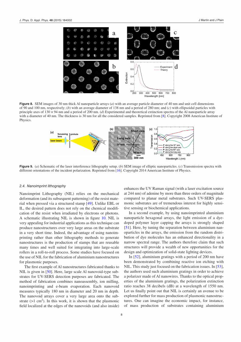
relies on complex facilities that are seldom available. Using EUV IL, arrays of aluminium nanoparticles with sizes down to 40 nm and well-defined geometries have been deposited over large areas [8] as illustrated in figure 8. In this work, EUV IL has been used to create arrays of nanoholes in the resist, and the subsequent evaporation led to the aluminium nanoparticle arrays. These nanoparticles exhibit strong and sharp plasmonic resonances in the near and mid-UV spectral regions as confirmed by experiments and theory.
The same group has also developed another method based on EUV IL and thermal evaporation for the fabrication of large area, free-standing aluminium nanohole arrays [48]. Here, the method consists of (1) the deposition of the resist layer on a thin Si3N4 membrane, (2) the creation of hole (110 nm depth) arrays in the layer of resist by EUV IL exposure (and the subsequent resist development) and (3) Al evaporation at an oblique angle while the substrate is rotated around the normal direction. Due to a self-shadowing effect during the film evaporation, the holes in the photoresist are still open after the aluminium deposition. This results in nanohole arrays in the aluminium film. The Si3N4 membrane and the resist are then removed by reactive ion etching from the backside during the last step, resulting in a free-standing aluminium nanomesh as shown in [48]. The UV plasmonic properties of the aluminium nanomesh are characterized using optical transmission meas-urements. A final example of aluminium nanostructures made by EUV-IL can be found in [20]. Here, aluminium nanodisks sustaining dipolar and quadrupolar plasmonic resonances located in the near and mid UV, respectively, are used for SERS operating at 257.2 nm.
A simpler IL setup, particularly for the source, can be used for the fabrication of aluminium nanostructures [16]. Its principle is described in figure 9(a): A laser beam (operating at 266 nm) is expanded and then spatially filtered. Using a Lloyds mirror setup, the beam is divided in two parts. The first one is directly incident on the sample and the second one is reflected by a mirror which is perpendicular to the substrate. Consequently, light interferences are generated, which create a sinusoidal distribution of the irradiation with a given perio-dicity in the resist. This periodicity is adjustable by changing the angle of incidence θ of the laser beam. The resist is then developed, resulting in nanohole arrays which will serve as the evaporation (or etch) mask. This method is more convenient that the previous one (EUV IL) as the optical setup, particu-larly the source, is more straightforward and available. With this method, they produced aluminium nanostructures of var-ious geometries: disks, quadratic and elliptic forms. The size of the nanostructures are larger compared with those obtained using EUV IL, with a typical minimum dimension equal to 120 nm. Consequently, the plasmonic properties of such Al nanostructures are located in the visible region, at least for their dipolar resonances. However, the nanostructures are very regular and uniform, and are consequently suitable for full systematic study. There are many optical characterizations in this work, and here we show only an example of transmission measurements performed on elliptic aluminium nanoparticles exhibiting polarization-dependent plasmonic resonances as illustrated in figures 9(b) and (c).
Figure 7. SEM micrographs of Al nanodisks with a mean diameter (a) D = 61 nm and h = 20 nm and (b) for D = 115 nm and h = 20 nm. (c) Measured extinction efficiencies for Al nanodisks for a range of disk diameters 61 nm < D < 492 nm at constant height h = 20 nm. Reprinted from [7]. Copyright 2008 American Chemical Society.
J. Phys. D: Appl. Phys. 48 (2015) 184002
J Martin and J Plain
8
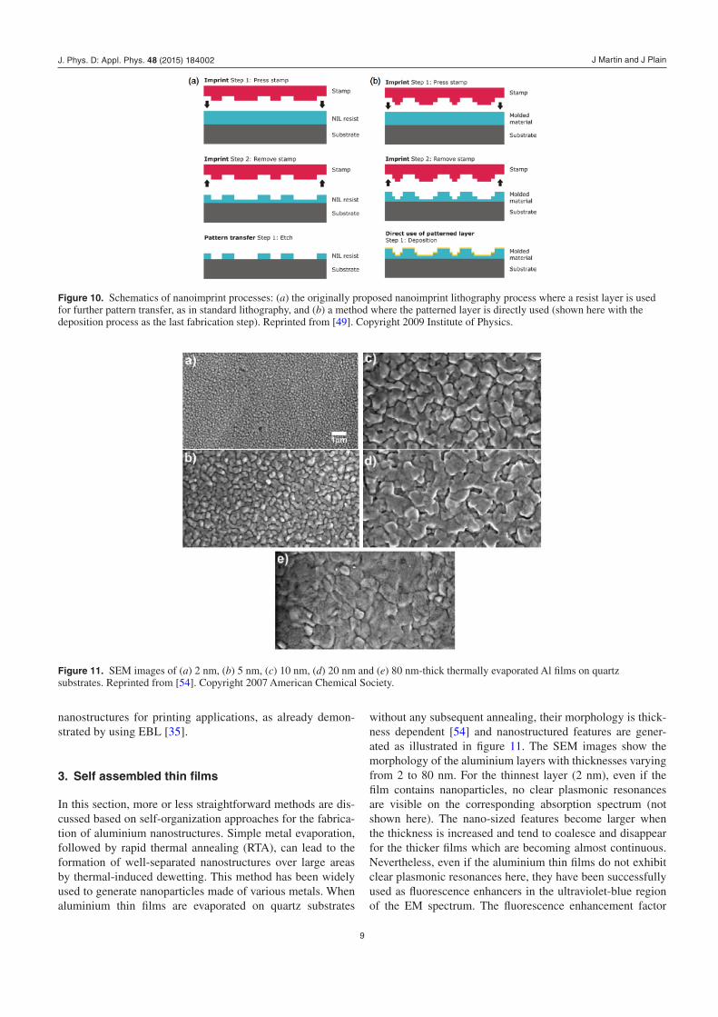
2.4. Nanoimprint lithography
Nanoimprint Lithography (NIL) relies on the mechanical deformation (and its subsequent patterning) of the resist mate-rial when pressed via a structured stamp [49]. Unlike EBL or IL, the desired pattern does not rely on the chemical modifi-cation of the resist when irradiated by electrons or photons. A schematic illustrating NIL is shown in figure 10. NIL is very appealing for industrial applications as this technique can produce nanostructures over very large areas on the substrate in a very short time. Indeed, the advantage of using nanoim-printing rather than other lithography methods to generate nanostructures is the production of stamps that are reusable many times and well suited for integrating into large-scale rollers in a roll-to-roll process. Some studies have focused on the use of NIL for the fabrication of aluminium nanostructures for plasmonic purposes.
The first example of Al nanostructures fabricated thanks to NIL is given in [50]. Here, large scale Al nanovoid-type sub-strates for UV-SERS detection purposes are fabricated. The method of fabrication combines nanoassembly, ion milling, nanoimprinting and e-beam evaporation. Each nanovoid measures typically 180 nm in diameter and 20 nm in depth. The nanovoid arrays cover a very large area onto the sub-strate (>1 cm2). In this work, it is shown that the plasmonic field localized at the edges of the nanovoids (and also inside)
enhances the UV Raman signal (with a laser excitation source at 244 nm) of adenine by more than three orders of magnitude compared to planar metal substrates. Such UV-SERS plas-monic substrates are of tremendous interest for highly sensi-tive sensing or biochemical applications.
In a second example, by using nanoimprinted aluminium nanoparticle hexagonal arrays, the light emission of a dye-doped polymer layer capping the arrays is strongly shaped [51]. Here, by tuning the separation between aluminium nan-oparticles in the arrays, the emission from the random distri-bution of dye molecules has an enhanced directionality in a narrow spectral range. The authors therefore claim that such structures will provide a wealth of new opportunities for the design and optimization of solid-state lighting devices.
In [52], aluminium gratings with a period of 200 nm have been demonstrated by combining reactive ion etching with NIL. This study just focused on the fabrication issues. In [53], the authors used such aluminium gratings in order to achieve a polarizer made of Al nanowires. Thanks to the optical prop-erties of the aluminium gratings, the polarization extinction ratio reaches 38 decibels (dB) at a wavelength of 1550 nm. Let us finally point out that NIL is certainly an avenue to be explored further for mass production of plasmonic nanostruc-tures. One can imagine the economic impact, for instance, of mass production of substrates containing aluminium
Figure 8. SEM images of 30 nm thick Al nanoparticle arrays (a) with an average particle diameter of 40 nm and unit cell dimensions of 90 and 100 nm, respectively; (b) with an average diameter of 138 nm and a period of 280 nm; and (c) with ellipsoidal particles with principle axes of 130 × 94 nm and a period of 200 nm. (d) Experimental and theoretical extinction spectra of the Al nanoparticle array with a diameter of 40 nm. The thickness is 30 nm for all the considered samples. Reprinted from [8]. Copyright 2008 American Institute of Physics.
Figure 9. (a) Schematic of the laser interference lithography setup. (b) SEM image of elliptic nanoparticles. (c) Transmission spectra with different orientations of the incident polarization. Reprinted from [16]. Copyright 2014 American Institute of Physics.
J. Phys. D: Appl. Phys. 48 (2015) 184002
J Martin and J Plain
9
nanostructures for printing applications, as already demon-strated by using EBL [35].
3. Self assembled thin films
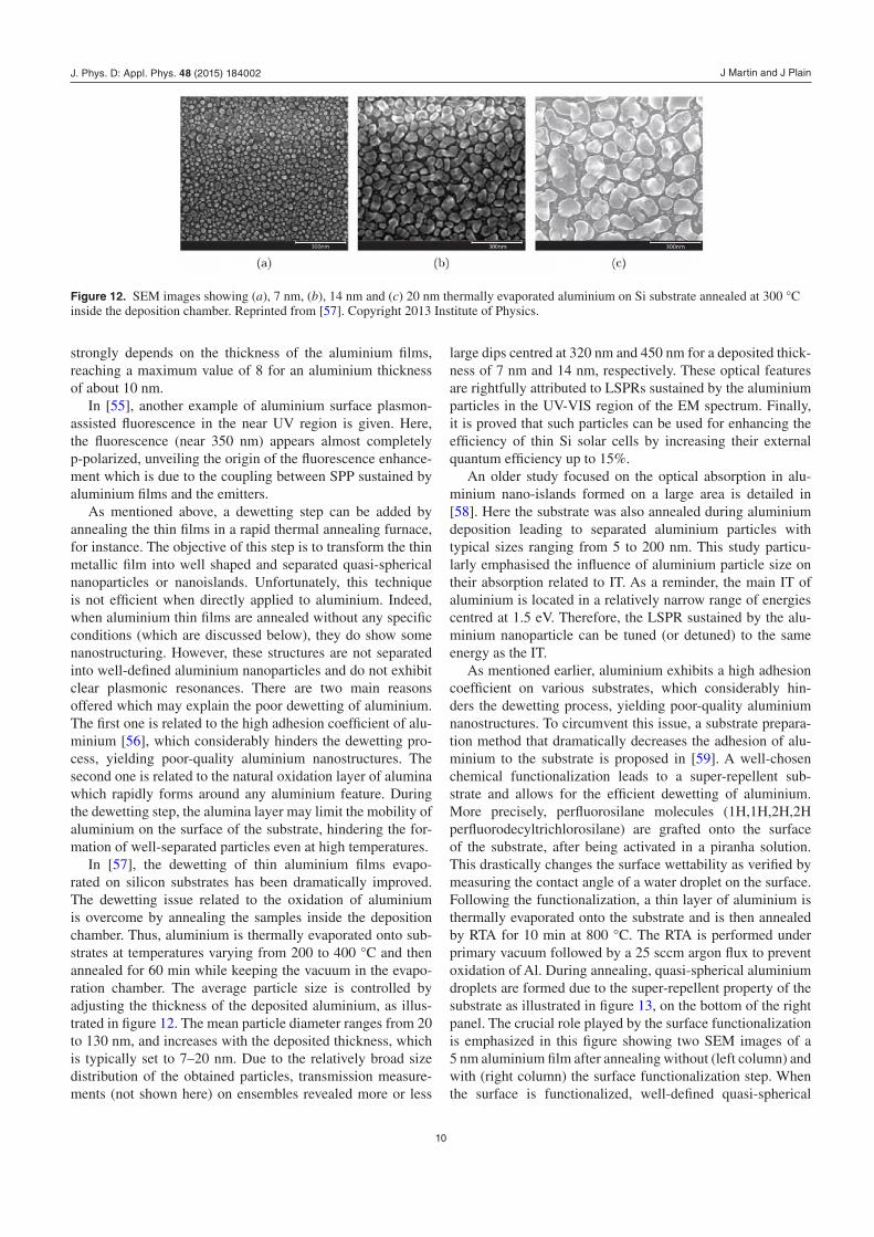
In this section, more or less straightforward methods are dis-cussed based on self-organization approaches for the fabrica-tion of aluminium nanostructures. Simple metal evaporation, followed by rapid thermal annealing (RTA), can lead to the formation of well-separated nanostructures over large areas by thermal-induced dewetting. This method has been widely used to generate nanoparticles made of various metals. When aluminium thin films are evaporated on quartz substrates
without any subsequent annealing, their morphology is thick-ness dependent [54] and nanostructured features are gener-ated as illustrated in figure 11. The SEM images show the morphology of the aluminium layers with thicknesses varying from 2 to 80 nm. For the thinnest layer (2 nm), even if the film contains nanoparticles, no clear plasmonic resonances are visible on the corresponding absorption spectrum (not shown here). The nano-sized features become larger when the thickness is increased and tend to coalesce and disappear for the thicker films which are becoming almost continuous. Nevertheless, even if the aluminium thin films do not exhibit clear plasmonic resonances here, they have been successfully used as fluorescence enhancers in the ultraviolet-blue region of the EM spectrum. The fluorescence enhancement factor
Figure 10. Schematics of nanoimprint processes: (a) the originally proposed nanoimprint lithography process where a resist layer is used for further pattern transfer, as in standard lithography, and (b) a method where the patterned layer is directly used (shown here with the deposition process as the last fabrication step). Reprinted from [49]. Copyright 2009 Institute of Physics.
Figure 11. SEM images of (a) 2 nm, (b) 5 nm, (c) 10 nm, (d) 20 nm and (e) 80 nm-thick thermally evaporated Al films on quartz substrates. Reprinted from [54]. Copyright 2007 American Chemical Society.
J. Phys. D: Appl. Phys. 48 (2015) 184002
J Martin and J Plain
10
strongly depends on the thickness of the aluminium films, reaching a maximum value of 8 for an aluminium thickness of about 10 nm.
In [55], another example of aluminium surface plasmon-assisted fluorescence in the near UV region is given. Here, the fluorescence (near 350 nm) appears almost completely p-polarized, unveiling the origin of the fluorescence enhance-ment which is due to the coupling between SPP sustained by aluminium films and the emitters.
As mentioned above, a dewetting step can be added by annealing the thin films in a rapid thermal annealing furnace, for instance. The objective of this step is to transform the thin metallic film into well shaped and separated quasi-spherical nanoparticles or nanoislands. Unfortunately, this technique is not efficient when directly applied to aluminium. Indeed, when aluminium thin films are annealed without any specific conditions (which are discussed below), they do show some nanostructuring. However, these structures are not separated into well-defined aluminium nanoparticles and do not exhibit clear plasmonic resonances. There are two main reasons offered which may explain the poor dewetting of aluminium. The first one is related to the high adhesion coefficient of alu-minium [56], which considerably hinders the dewetting pro-cess, yielding poor-quality aluminium nanostructures. The second one is related to the natural oxidation layer of alumina which rapidly forms around any aluminium feature. During the dewetting step, the alumina layer may limit the mobility of aluminium on the surface of the substrate, hindering the for-mation of well-separated particles even at high temperatures.
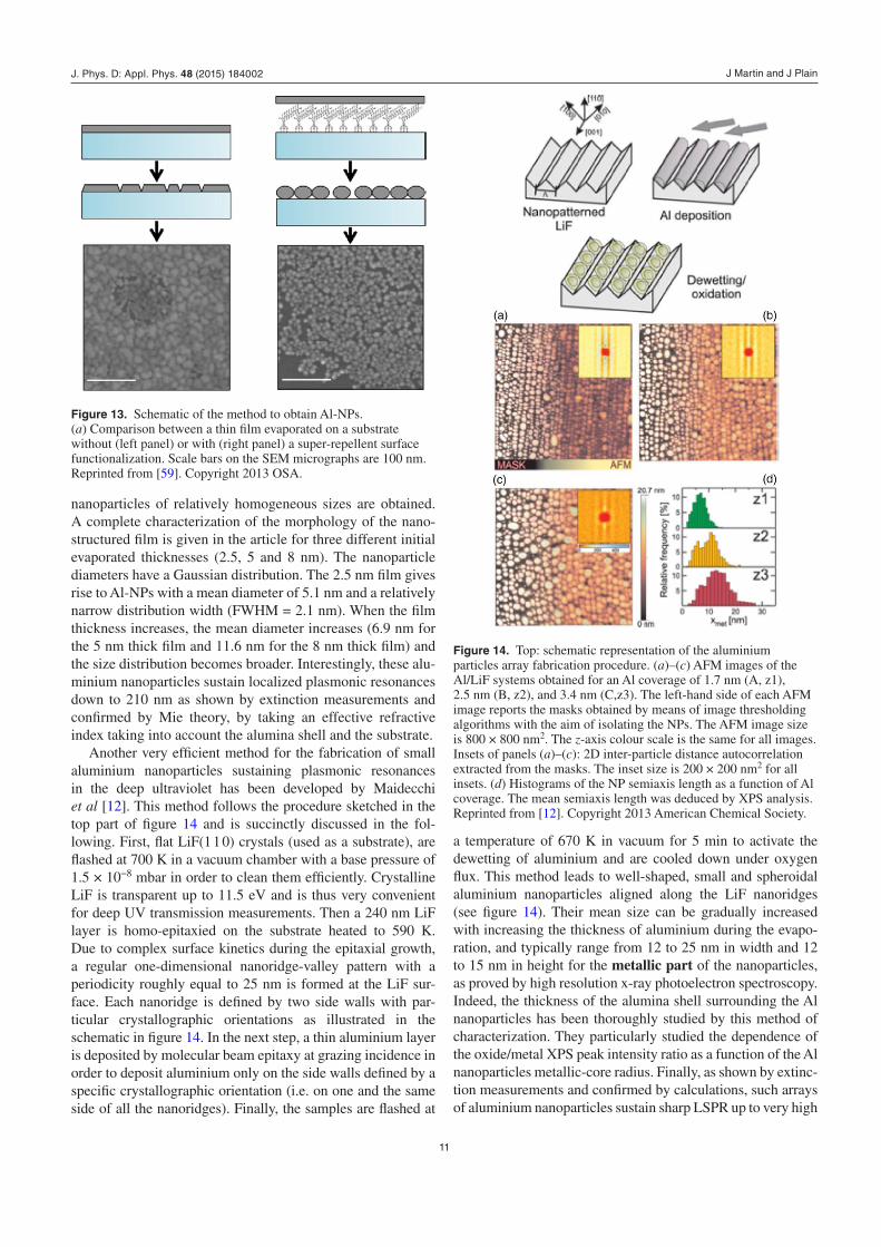
In [57], the dewetting of thin aluminium films evapo-rated on silicon substrates has been dramatically improved. The dewetting issue related to the oxidation of aluminium is overcome by annealing the samples inside the deposition chamber. Thus, aluminium is thermally evaporated onto sub-strates at temperatures varying from 200 to 400 °C and then annealed for 60 min while keeping the vacuum in the evapo-ration chamber. The average particle size is controlled by adjusting the thickness of the deposited aluminium, as illus-trated in figure 12. The mean particle diameter ranges from 20 to 130 nm, and increases with the deposited thickness, which is typically set to 7–20 nm. Due to the relatively broad size distribution of the obtained particles, transmission measure-ments (not shown here) on ensembles revealed more or less
large dips centred at 320 nm and 450 nm for a deposited thick-ness of 7 nm and 14 nm, respectively. These optical features are rightfully attributed to LSPRs sustained by the aluminium particles in the UV-VIS region of the EM spectrum. Finally, it is proved that such particles can be used for enhancing the efficiency of thin Si solar cells by increasing their external quantum efficiency up to 15%.
An older study focused on the optical absorption in alu-minium nano-islands formed on a large area is detailed in [58]. Here the substrate was also annealed during aluminium deposition leading to separated aluminium particles with typical sizes ranging from 5 to 200 nm. This study particu-larly emphasised the influence of aluminium particle size on their absorption related to IT. As a reminder, the main IT of aluminium is located in a relatively narrow range of energies centred at 1.5 eV. Therefore, the LSPR sustained by the alu-minium nanoparticle can be tuned (or detuned) to the same energy as the IT.
As mentioned earlier, aluminium exhibits a high adhesion coefficient on various substrates, which considerably hin-ders the dewetting process, yielding poor-quality aluminium nanostructures. To circumvent this issue, a substrate prepara-tion method that dramatically decreases the adhesion of alu-minium to the substrate is proposed in [59]. A well-chosen chemical functionalization leads to a super-repellent sub-strate and allows for the efficient dewetting of aluminium. More precisely, perfluorosilane molecules (1H,1H,2H,2H perfluorodecyltrichlorosilane) are grafted onto the surface of the substrate, after being activated in a piranha solution. This drastically changes the surface wettability as verified by measuring the contact angle of a water droplet on the surface. Following the functionalization, a thin layer of aluminium is thermally evaporated onto the substrate and is then annealed by RTA for 10 min at 800 °C. The RTA is performed under primary vacuum followed by a 25 sccm argon flux to prevent oxidation of Al. During annealing, quasi-spherical aluminium droplets are formed due to the super-repellent property of the substrate as illustrated in figure 13, on the bottom of the right panel. The crucial role played by the surface functionalization is emphasized in this figure showing two SEM images of a 5 nm aluminium film after annealing without (left column) and with (right column) the surface functionalization step. When the surface is functionalized, well-defined quasi-spherical
Figure 12. SEM images showing (a), 7 nm, (b), 14 nm and (c) 20 nm thermally evaporated aluminium on Si substrate annealed at 300 °C inside the deposition chamber. Reprinted from [57]. Copyright 2013 Institute of Physics.
J. Phys. D: Appl. Phys. 48 (2015) 184002
J Martin and J Plain
11
nanoparticles of relatively homogeneous sizes are obtained. A complete characterization of the morphology of the nano-structured film is given in the article for three different initial evaporated thicknesses (2.5, 5 and 8 nm). The nanoparticle diameters have a Gaussian distribution. The 2.5 nm film gives rise to Al-NPs with a mean diameter of 5.1 nm and a relatively narrow distribution width (FWHM = 2.1 nm). When the film thickness increases, the mean diameter increases (6.9 nm for the 5 nm thick film and 11.6 nm for the 8 nm thick film) and the size distribution becomes broader. Interestingly, these alu-minium nanoparticles sustain localized plasmonic resonances down to 210 nm as shown by extinction measurements and confirmed by Mie theory, by taking an effective refractive index taking into account the alumina shell and the substrate.
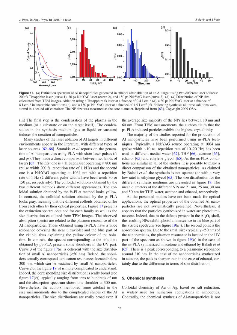
Another very efficient method for the fabrication of small aluminium nanoparticles sustaining plasmonic resonances in the deep ultraviolet has been developed by Maidecchi et al [12]. This method follows the procedure sketched in the top part of figure 14 and is succinctly discussed in the fol-lowing. First, flat LiF(1 1 0) crystals (used as a substrate), are flashed at 700 K in a vacuum chamber with a base pressure of 1.5 × 10⁻⁸ mbar in order to clean them efficiently. Crystalline LiF is transparent up to 11.5 eV and is thus very convenient for deep UV transmission measurements. Then a 240 nm LiF layer is homo-epitaxied on the substrate heated to 590 K. Due to complex surface kinetics during the epitaxial growth, a regular one-dimensional nanoridge-valley pattern with a periodicity roughly equal to 25 nm is formed at the LiF sur-face. Each nanoridge is defined by two side walls with par-ticular crystallographic orientations as illustrated in the schematic in figure 14. In the next step, a thin aluminium layer is deposited by molecular beam epitaxy at grazing incidence in order to deposit aluminium only on the side walls defined by a specific crystallographic orientation (i.e. on one and the same side of all the nanoridges). Finally, the samples are flashed at
a temperature of 670 K in vacuum for 5 min to activate the dewetting of aluminium and are cooled down under oxygen flux. This method leads to well-shaped, small and spheroidal aluminium nanoparticles aligned along the LiF nanoridges (see figure 14). Their mean size can be gradually increased with increasing the thickness of aluminium during the evapo-ration, and typically range from 12 to 25 nm in width and 12 to 15 nm in height for the metallic part of the nanoparticles, as proved by high resolution x-ray photoelectron spectroscopy. Indeed, the thickness of the alumina shell surrounding the Al nanoparticles has been thoroughly studied by this method of characterization. They particularly studied the dependence of the oxide/metal XPS peak intensity ratio as a function of the Al nanoparticles metallic-core radius. Finally, as shown by extinc-tion measurements and confirmed by calculations, such arrays of aluminium nanoparticles sustain sharp LSPR up to very high
Figure 13. Schematic of the method to obtain Al-NPs. (a) Comparison between a thin film evaporated on a substrate without (left panel) or with (right panel) a super-repellent surface functionalization. Scale bars on the SEM micrographs are 100 nm. Reprinted from [59]. Copyright 2013 OSA.
Figure 14. Top: schematic representation of the aluminium particles array fabrication procedure. (a)–(c) AFM images of the Al/LiF systems obtained for an Al coverage of 1.7 nm (A, z1), 2.5 nm (B, z2), and 3.4 nm (C,z3). The left-hand side of each AFM image reports the masks obtained by means of image thresholding algorithms with the aim of isolating the NPs. The AFM image size is 800 × 800 nm2. The z-axis colour scale is the same for all images. Insets of panels (a)–(c): 2D inter-particle distance autocorrelation extracted from the masks. The inset size is 200 × 200 nm2 for all insets. (d) Histograms of the NP semiaxis length as a function of Al coverage. The mean semiaxis length was deduced by XPS analysis. Reprinted from [12]. Copyright 2013 American Chemical Society.
J. Phys. D: Appl. Phys. 48 (2015) 184002

J Martin and J Plain
12
energies (up to 5.8 eV), and are thus very appealing for deep ultraviolet plasmonics. In this study, optical characterizations and calculations are very much complete and deeply analysed, but as we focus on the fabrication in this review all the details can be retrieved in the corresponding [12].
A final example of self-assembled Al structures is given in [60]. Here, evaporation-induced rapid self-assembly of microwires made of Al nanoparticles (commercially pur-chased under the form of Al powder) was demonstrated under microwave heating. By using different surfactant-solvent for-mulations, the microwires are formed on the substrate at the contact line between the solvent containing the powder and the air due to stick-slip dynamics during the heating. These mechanisms are very well described in the paper. The typical width of the microwires is 1–20 μm, and the distance between the microwires is typically 50–300 μm.
4. Laser ablation
Historically, it appears that one of the first developed tech-niques for the mass production of Al nanoparticles is the pulsed laser ablation (PLA) technique. In addition, this tech-nique, well known and well documented, has been widely used in different communities, including nanooptics, to gen-erate nanoparticles of various materials [61]. This technique relies on the interaction of a pulsed laser beam with a solid target. The ablation takes place in several steps which are summarized in figure 15. (i) the first one is the generation of a plasma induced by the laser on the surface of the target. (ii)
The second one is the laser-induced expansion of the plasma plume in the medium (liquid or gas or vacuum). The plasma expansion will vary from one medium to another [62]. For instance, the plasma expansion has been imaged during the PLA process in air and in water as shown in figure 16 [62].
Figure 15. The evolution of the laser-induced plasma in liquid. (a) The generation of the laser-induced plasma due to the irradiation of the front part of the laser pulse on the target. (b) The expansion of the plasma plume in liquid due to absorption of the later laser pulse and the plasma-induced pressure created by the shock wave. (c) Four kinds of chemical reactions taking place inside the plasma and liquid, and the interface between the plasma and liquid. (d) Two condensations of the plasma plume in liquid: one is used to prepare surface coatings on the target surface, and the other one is used to fabricate nanoparticles in liquid. Inspired by [61].
Figure 16. Images of plasma plume at various time delays in ambient air and water. Reprinted from [62]. Copyright 2010 American Institute of Physics.
J. Phys. D: Appl. Phys. 48 (2015) 184002
J Martin and J Plain
13
(iii) The final step is the condensation of the plasma in the medium (or a substrate or on the target itself). The conden-sation in the synthesis medium (gas or liquid or vacuum) induces the creation of nanoparticles.
Many studies of the laser ablation of Al targets in different environments appear in the literature, with different types of laser sources [62–66]. Stratakis et al reports on the genera-tion of Al nanoparticles using PLA with short laser pulses (fs and ps). They made a direct comparison between two kinds of lasers [63]. The first one is a Ti:Saph laser operating at 800 nm (pulse width 200 fs, repetition rate of 1 kHz) and the second one is a Nd:YAG operating at 1064 nm with a repetition rate of 1 Hz (2 different pulse widths have been used/ 30 or 150 ps, respectively). The colloidal solutions obtained by the two different methods show different appearances. The col-loidal solution obtained by the fs-PLA method looks yellow. In contrast, the colloidal solution obtained by the ps-PLA looks gray, meaning that the different colloids obtained differ from each other by their optical properties. Figure 17 presents the extinction spectra obtained for each family as well as the size distribution calculated from TEM images. The observed absorption spectra are related to the plasmon resonance of the Al nanoparticles. Those obtained using fs-PLA have a wide resonance covering the near ultraviolet and the blue part of the visible, thus explaining the yellow colour of the solu-tion. In contrast, the spectra corresponding to the solutions obtained by ps-PLA present some shoulders in the UV part. Curve 3 of the figure 17(a) is coherent with the size distribu-tion of small Al nanoparticles (<50 nm). Indeed, the shoul-ders actually correspond to plasmon resonances located below 300 nm, which can be sustained by small Al nanoparticles. Curve 2 of the figure 17(a) is more complicated to understand. Indeed, the corresponding size distribution is really broad (see figure 17(c)), typically ranging from tens to hundreds of nm and the absorption spectrum shows one shoulder at 300 nm. Nevertheless, the authors mentioned some artefact in the size measurements due to the complicated shapes of the Al nanoparticles. The size distributions are really broad even if
the average size majority of the NPs lies between 10 nm and 60 nm. From TEM measurements, the authors claim that the ps-PLA induced particles exhibit the highest crystallinity.
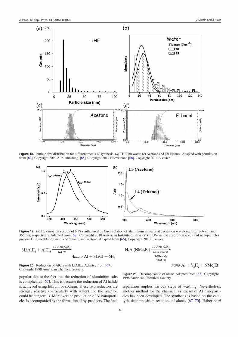
The majority of the studies reported for the production of Al nanoparticles have been performed using ns-PLA tech-niques. Typically, a Nd:YAG source operating at 1064 nm (pulse width ∼10 ns, repetition rate of 10–20 Hz) has been used in different media: water [62], THF [66], acetone [65], ethanol [65] and ethylene glycol [65]. As the ns-PLA condi-tions are similar in all of the studies, it is possible to make a direct comparison of the obtained nanoparticles. As claimed by Baladi et al, the synthesis is not operant (or with a very low rate) in ethylene glycol [65]. The size distribution for the different synthesis mediums are presented in figure 18. The mean diameters of the different NPs are 21 nm, 25 nm, 30 nm and 50 nm for THF, water, acetone and ethanol, respectively.
As the presented studies have not been made for optical applications, the optical properties of the obtained Al nano-particles are not systematically presented. Nevertheless, it appears that the particles synthesized in water are photolumi-nescent. Indeed, due to the defects present in the Al2O3 shell, the resulting NPs exhibit photoluminescence in the blue part of the visible spectrum (see figure 19(a)). The second point is the absorption spectra. Due to the small size (typically <50 nm) of the nanoparticles, the plasmon resonance is located in the UV part of the spectrum as shown in figure 19(b) in the case of the ns-PLA synthesized in acetone and ethanol by Baladi et al [65]. There is a peak corresponding to a plasmonic resonance around 210 nm. In the case of the nanoparticles synthesized in acetone, the peak is sharper than in the case of ethanol, cer-tainly due to the difference in terms of size distribution.
5. Chemical synthesis
Colloidal chemistry of Au or Ag, based on salt reduction, is widely used for numerous applications in nanooptics. Contrarily, the chemical synthesis of Al-nanoparticles is not
Figure 17. (a) Extinction spectrum of Al nanoparticles generated in ethanol after ablation of an Al target using two different laser sources: 200 fs Ti:sapphire laser (curve 1), 30 ps Nd:YAG laser (curve 2), and 150 ps Nd:YAG laser (curve 3). (b)–(d) Distribution of NP size calculated from TEM images. Ablation using a Ti:sapphire fs laser at a fluence of 0.4 J cm−2 (b), a 30 ps Nd:YAG laser at a fluence of 8 J cm−2 in anaerobic conditions (c), and a 150 ps Nd:YAG laser at a fluence of 1.5 J cm2 (d). Following synthesis all three solutions were stored in a sealed-off container. The NP size was measured as the core diameter. Reprinted from [63], Copyright 2009 OSA.
J. Phys. D: Appl. Phys. 48 (2015) 184002
J Martin and J Plain
14
popular due to the fact that the reduction of aluminium salts is complicated [67]. This is because the reduction of Al halide is achieved using lithium or sodium. These two reductors are strongly reactive (particularly with water) and the reaction could be dangerous. Moreover the production of Al nanoparti-cles is accompanied by the formation of by-products. The final
separation implies various steps of washing. Nevertheless, another method for the chemical synthesis of Al nanoparti-cles has been developed. The synthesis is based on the cata-lytic decomposition reactions of alanes [67–70]. Haber et al
Figure 18. Particle size distribution for different media of synthesis. (a) THF, (b) water, (c) Acetone and (d) Ethanol. Adapted with permission from [62], Copyright 2010 AIP Publishing, [65], Copyright 2014 Elsevier and [66], Copyright 2014 Elsevier.
Figure 19. (a) PL emission spectra of NPs synthesized by laser ablation of aluminium in water at excitation wavelengths of 266 nm and 355 nm, respectively. Adapted from [62], Copyright 2010 American Institute of Physics. (b) UV-visible absorption spectra of nanoparticles prepared in two ablation media of ethanol and acetone. Adapted from [65], Copyright 2010 Elsevier.
Figure 20. Reduction of AlCl3 with LiAlH4. Adapted from [67], Copyright 1998 American Chemical Society.
Figure 21. Decomposition of alane. Adapted from [67], Copyright 1998 American Chemical Society.
J. Phys. D: Appl. Phys. 48 (2015) 184002
J Martin and J Plain
15
have shown the possibility of reducing AlCl3 with LiAlH4 according to the reaction presented in figure 20. Haber et al claim that the reaction presented in figure 20 proceeded by the intermediate formation and decomposition of alanes, AlH3.
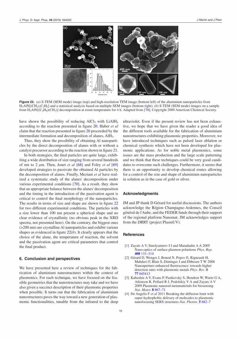
Thus, they show the possibility of obtaining Al nanoparti-cles by the direct decomposition of alanes with or without a catalyst precursor according to the reaction shown in figure 21.
In both strategies, the final particles are quite large, exhib-iting a wide distribution of size ranging from several hundreds of nm to 2 µm. Then, Jouet et al [68] and Foley et al [69] developed strategies to passivate the obtained Al particles by the decomposition of alanes. Finally, Meziani et al have real-ized a systematic study of the alanes' decomposition under various experimental conditions [70]. As a result, they show that an appropriate balance between the alanes' decomposition and the timing in the introduction of the passivation agent is critical to control the final morphology of the nanoparticles. The results in terms of size and shape are shown in figure 22 for two different experimental conditions. The particles with a size lower than 100 nm present a spherical shape and no clear evidence of crystallinity (no obvious peak in the XRD spectra, not presented here). On the contrary, the biggest ones (>200 nm) are crystalline Al nanoparticles and exhibit various shapes as evidenced in figure 22(b). It clearly appears that the choice of the alane, the temperature of reaction, the solvent and the passivation agent are critical parameters that control the final product.
6. Conclusion and perspectives
We have presented here a review of techniques for the fab-rication of aluminium nanostructures within the context of plasmonics. For each technique, we have focused on the fea-sible geometries that the nanostructures may take and we have also given a succinct description of their plasmonic properties when possible. It turns out that the fabrication of aluminium nanostructures paves the way toward a new generation of plas-monic functionalities, tunable from the infrared to the deep
ultraviolet. Even if the present review has not been exhaus-tive, we hope that we have given the reader a good idea of the different tools available for the fabrication of aluminium nanostructures exhibiting plasmonic properties. Moreover, we have introduced techniques such as pulsed laser ablation or chemical synthesis which have not been developed for plas-monic applications. As for noble metal plasmonics, some issues are the mass production and the large scale patterning and we think that these techniques could be very good candi-dates to overcome such challenges. Furthermore, it seems that there is an opportunity to develop chemical routes allowing for a control of the size and shape of aluminium nanoparticles in solution as in the case of gold or silver.
Acknowledgments
JM and JP thank D Gérard for useful discussions. The authors acknowledge the Région Champagne-Ardennes, the Conseil général de l'Aube, and the FEDER funds through their support of the regional platform Nanomat. JM acknowledges support from the DRRT (project PlasmUV).
References
[1] Zayats A V, Smolyaninov I I and Maradudin A A 2005 Nano-optics of surface plasmon polaritons Phys. Rep. 408 131–314
[2] Gérard D, Wenger J, Bonod N, Popov E, Rigneault H, Mahdavi F, Blair S, Dintinger J and Ebbesen T W 2008 Nanoaperture-enhanced fluorescence: towards higher detection rates with plasmonic metals Phys. Rev. B 77 045413
[3] Kabashin A V, Evans P, Pastkovsky S, Hendren W, Wurtz G A, Atkinson R, Pollard R J, Podolskiy V A and Zayats A V 2009 Plasmonic nanorod metamaterials for biosensing Nat. Mater. 8 867–71
[4] De Angelis F et al 2011 Breaking the diffusion limit with super-hydrophobic delivery of molecules to plasmonic nanofocusing SERS structures Nat. Photon. 5 682–7
Figure 22. (a) S-TEM (SEM mode) image (top) and high-resolution TEM image (bottom left) of the aluminium nanoparticles from H3AlN[(CH3)2C2H5] and a statistical analysis based on multiple SEM images (bottom right). (b) S-TEM (SEM mode) images on a sample from H3AlN[(C4H8)(CH3)] decomposition at room temperature for 4 h. Adapted from [70], Copyright 2009 American Chemical Society.
J. Phys. D: Appl. Phys. 48 (2015) 184002

J Martin and J Plain
16
[5] Ehrenreich H, Philipp H R and Segall B 1963 Optical Properties of aluminium Phys. Rev. 132 1918–28
[6] Batson P E 1982 A new surface plasmon resonance in clusters of small aluminium spheres Ultramicroscopy 9 277–82
[7] Langhammer C, Schwind M, Kasemo B and Zorić I 2008 Localized surface plasmon resonances in aluminium nanodisks Nano Lett. 8 1461–71
[8] Ekinci Y, Solak H H and Löffler J F 2008 Plasmon resonances of aluminium nanoparticles and nanorods J. Appl. Phys. 104 083107
[9] Chan G H, Zhao J, Schatz G C and Van Duyne R P 2008 Localized surface plasmon resonance spectroscopy of triangular aluminium nanoparticles J. Phys. Chem. C 112 13958–63
[10] Taguchi A, Saito Y, Watanabe K, Yijian S and Kawata S 2012 Tailoring plasmon resonances in the deep-ultraviolet by size-tunable fabrication of aluminium nanostructures Appl. Phys. Lett. 101 081110
[11] Knight M W, Liu L, Wang Y, Brown L, Mukherjee S, King N S, Everitt H O, Nordlander P and Halas N J 2012 Aluminium plasmonic nanoantennas Nano Lett. 12 6000–4
[12] Maidecchi G et al 2013 ACS Nano 7 5834–41 [13] Ross M B and Schatz G C 2014 Aluminium and indium
plasmonic nanoantennas in the ultraviolet J. Phys. Chem. C 118 12506–14
[14] Knight M W, King N S, Liu L, Everitt H O, Nordlander P and Halas N J 2014 Aluminium for plasmonics ACS Nano 8 834–40
[15] Lecarme O, Sun Q, Ueno K and Misawa H 2014 Robust and versatile light absorption at near-infrared wavelengths by plasmonic aluminum nanorods ACS Photon. 1 538–46
[16] Schade M, Fuhrmann B, Bohley C, Schlenker S, Sardana N, Schilling J and Leipner H S 2014 Regular arrays of Al nanoparticles for plasmonic applications J. Appl. Phys. 115 084309
[17] Lawrie B J, Kim K W, Norton D P and Haglund R F Jr 2012 Plasmon-exciton hybridization in ZnO quantum-well Al nanodisc heterostructures Nano Lett. 12 6152–7
[18] Okamoto K, Niki I, Shvartser A, Narukawa Y, Mukai T and Scherer A 2004 Surface-plasmon-enhanced light emitters based on InGaN quantum wells Nat. Mater. 3 601–5
[19] Taguchi A, Hayazawa N, Furusawa K, Ishitobi H and Kawata S 2009 Deep-UV tip: enhanced Raman scattering J. Raman Spectrosc. 40 1324–30
[20] Jha S K, Ahmed Z, Agio M, Ekinci Y and Löffler J F 2012 Deep-UV surface-enhanced resonance Raman scattering of Adenine on aluminium nanoparticle arrays J. Am. Chem. Soc. 134 1966–9
[21] Chowdhury M H, Ray K, Gray S K, Pond J and Lakowicz J R 2009 Anal. Chem. 81 1397–403
[22] Canalejas-Tejero V, Herranz S, Bellingham A, Cruz Moreno-Bondi M and Angulo Barrios C 2014 Passivated aluminium nanohole arrays for label-free biosensing applications ACS Appl. Mater. Interfaces 6 1005–10
[23] Castro-Lopez M, Brinks D, Sapienza R and van Hulst N F 2011 Aluminium for nonlinear plasmonics: resonance-driven polarized luminescence of Al, Ag, and Au nanoantennas Nano Lett. 11 4674–8
[24] Akimov Y A and Koh W S 2010 Resonant and nonresonant plasmonic nanoparticle enhancement for thin-film silicon solar cells Nanotechnology 21 235201
[25] Zheng B Y, Wang Y, Nordlander P and Halas N J 2014 Color-selective and CMOS-compatible photodetection based on aluminum plasmonics Adv. Mater. 26 6318–23
[26] Honda M, Kumamoto Y, Taguchi A, Saito Y and Kawata S 2014 Plasmon-enhanced UV photocatalysis Appl. Phys. Lett. 104 061108
[27] Miao L, Stoddart P R and Hsiang T Y 2014 Novel aluminium near field transducer and highly integrated
micro–nano-optics design for heat-assisted ultra-high-density magnetic recording Nanotechnology 25 295202
[28] Gérard D and Gray S 2015 Aluminium plasmonics J. Phys. D: Appl. Phys. 18 184001
[29] Lérondel G, Kostcheev S and Plain J 2012 Nanofabrication for plasmonics Plasmonics: from Basics to Advanced Topics (Springer Series in Optical Sciences vol 167) pp 269–316
[30] Zorić I, Zäch M, Kasemo B and Langhammer C 2011 Gold, platinum, and aluminium nanodisk plasmons: material independence, subradiance, and damping mechanisms ACS Nano 5 2535–46
[31] Li J T, Parisi J, Wang Z B and Pu Y K 2014 The energy evolution of surface plasmons on an oxidized aluminum surface: the role of the atomic polarizability of oxygen adsorbates and the thickness of the oxide layer J. Phys. D: Appl. Phys. 47 425304
[32] Rai A, Park K, Zhou L and Zachariah M R 2006 Understanding the mechanism of aluminium nanoparticle oxidation Combust. Theory Modelling 10 843–59
[33] Temple T L and Bagnall D M 2011 Optical properties of gold and aluminium nanoparticles for silicon solar cell applications J. Appl. Phys. 109 084343
[34] Martin J, Kociak M, Mahfoud Z, Proust J, Gérard D and Plain J 2014 High-resolution imaging and spectroscopy of multipolar plasmonic resonances in aluminum nanoantennas Nano Lett. 14 5517–23
[35] Tan S J, Zhang L, Zhu D, Goh X M, Wang Y M, Kumar K, Qiu C-W and Yang J K W 2014 Plasmonic color palettes for photorealistic printing with aluminium nanostructures Nano Lett. 14 4023–9
[36] Clausen J S, Højlund-Nielsen E, Christiansen A B, Yazdi S, Grajower M, Taha H, Levy U, Kristensen A and Mortensen N A 2014 Plasmonic metasurfaces for coloration of plastic consumer products Nano Lett. 14 4499–504
[37] Olson J, Manjavacas A, Liu L, Chang W S, Foerster B, King N S, Knight M W, Nordlander P, Halas N J and Link S 2014 Vivid, full-color aluminum plasmonic pixels Proc. Natl Acad. Sci. 111 14348–53
[38] Hulteen J C and Van Duyne P 1995 Nanosphere lithography: a materials general fabrication process for periodic particle array surfaces J. Vac. Sci. Technol. A 13 1553
[39] Haynes C L, Richard P and Van Duyne R P 2001 Nanosphere lithography: a versatile nanofabrication tool for studies of size-dependent nanoparticle optics J. Phys. Chem. B 105 5599–611
[40] Ye X and Qi L 2011 Two-dimensionally patterned nanostructures based on monolayer colloidal crystals: controllable fabrication, assembly and applications Nano Today 6 608–31
[41] Mak G Y, Fu W Y, Lam E Y and Choi H W 2009 Metallic nanoparticle array on GaN by microsphere lithography Phys. Status Solidi C 6 S654–7
[42] Hanarp P, Sutherland D S, Gold J and Kasemo B 2003 Control of nanoparticle film structure for colloidal lithography Colloids Surf. 214 23–36
[43] Schwind M, Kasemo B and Zorić I 2013 Localized and propagating plasmons in metal films with nanoholes Nano Lett. 13 1743–50
[44] Fredriksson H, Alaverdyan Y, Dmitriev A, Langhammer C, Sutherland D S, Zäch M and Kasemo B 2007 Hole-mask colloidal lithography Adv. Mater. 19 4297–302
[45] Rodriguez M, Furse C, Shumaker–Parry J S and Blair S 2014 Scaling the response of nanocrescent antennas into the ultraviolet ACS Photon. 1 496–506
[46] Yen A, Schattenburg M L and Henry I 1992 Proposed method for fabricating 50 nm-period gratings by achromatic holographic lithography Appl. Opt. 31 2972–3
[47] Solak H H, David C, Gobrecht J, Golovkina V, Cerrina F, Kim S O and Nealey P F 2003 Sub-50 nm period patterns
J. Phys. D: Appl. Phys. 48 (2015) 184002

J Martin and J Plain
17
with EUV interference lithography Microelectron. Eng. 67–8 56–62
[48] Ekinci Y, Solak H H and David C 2007 Extraordinary optical transmission in the ultraviolet region through aluminium hole arrays Opt. Lett. 32 172–4
[49] Boltasseva A 2009 Plasmonic components fabrication via nanoimprint J. Opt. A: Pure Appl. Opt. 11 114001
[50] Ding T, Sigle D O, Herrmann L O, Wolverson D and Baumberg J J 2014 Nanoimprint lithography of Al nanovoids for deep-UV SERS ACS Appl. Mater. Interfaces 6 17358–63
[51] Lozano G, Grzela G, Verschuuren M A, Ramezani M and Gómez Rivas J 2014 Tailor-made directional emission in nanoimprinted plasmonic-based light-emitting devices Nanoscale 6 9223
[52] Ahn S-W, Lee K-D, Kim J-S, Kim S H, Lee S H, Park J-D and Yoon P-W 2005 Fabrication of subwavelength aluminium wire grating using nanoimprint lithography and reactive ion etching Microelectron. Eng. 7879 314–8
[53] Kim J-S, Lee K-D, Ahn S-W, Kim S H, Park J-D, Lee S-E and Yoon S-S 2004 Fabrication of nanowire polarizer by using nanoimprint lithography J. Korean Phys. Soc. 45 S890–2
[54] Ray K, Chowdhury M H and JLakowicz J R 2007 Aluminium nanostructured films as substrates for enhanced fluorescence in the ultraviolet-blue spectral region Anal. Chem. 79 6480–7
[55] Malicka J, Gryczynski I, Gryczynski Z and Lakowicz J R 2004 Surface plasmon-coupled ultraviolet emission of 2,5–diphenyl–1,3,4–oxadiazole J. Phys. Chem. B 108 19114–8
[56] Bhushan B 2001 Handbook of Modern Tribology 1 (Boca Raton, FL: CRC)
[57] Villesen T F, Uhrenfeldt C, Johansen B and Nylandsted Larsen A 2013 Self-assembled Al nanoparticles on Si and fused silica, and their application for Si solar cells Nanotechnology 24 275606
[58] Anno E and Tanimoto M 2001 Size-dependent change in parallel band absorption of Al particles Phys. Rev. B 64 165407
[59] Martin J, Proust J, Gérard D and Plain J 2013 Localized surface plasmon resonances in the ultraviolet from large
scale nanostructured aluminium films Opt. Mater. Express 3 954–9
[60] Olgun U 2010 Rapid microwave-assisted deposition of microwire patterns of nanoaluminum and nanosilver from colloids ACS Appl. Mater. Interfaces 2 28–34
[61] Yang G 2007 Laser ablation in liquids: applications in the synthesis of nanocrystals Prog. Mater. Sci. 52 648–98
[62] Kumar B and Thareja R K 2010 Synthesis of nanoparticles in laser ablation of aluminum in liquid J. Appl. Phys. 108 064906
[63] Stratakis E, Barberoglou M, Fotakis C, Viau G, Garcia C and Shafeev G A 2009 Generation of Al nanoparticles via ablation of bulk Al in liquids with short laser pulses Opt. Express 17 12650–9
[64] Stratakis E, Zorba V, Barberoglou M, Fotakis C and Shafeev G A 2009 Laser writing of nanostructures on bulk Al via Its ablation in liquids Nanotechnology 20 105303
[65] Baladi A and Mamoory R S 2010 Investigation of different liquid media and ablation times on pulsed laser ablation synthesis of aluminum nanoparticles Appl. Surf. Sci. 256 7559–64
[66] Crouse C A, Shin E, Murray P T and Spowart J E 2010 Solution assisted laser ablation synthesis of discrete aluminum nanoparticles Mater. Lett. 64 271–4
[67] Haber J A and Buhro W E 1998 Kinetic instability of nanocrystalline aluminum prepared by chemical synthesis; facile room-temperature grain growth J. Am. Chem. Soc. 120 10847–55
[68] Jouet R J, Warren A D, Rosenberg D M, Bellitto V J, Park K and Zachariah M R 2005 Surface passivation of bare aluminum nanoparticles using perfluoroalkyl carboxylic acids Chem. Mater. 17 2987–96
[69] Foley T J, Johnson C E and Higa K T 2005 Inhibition of oxide formation on aluminum nanoparticles by transition metal coating Chem. Mater. 17 4086–91
[70] Meziani M J, Bunker C E, Lu F, Li H, Wang W, Guliants E A, Quinn R A and Sun Y-P 2009 Formation and properties of stabilized aluminum nanoparticles ACS Appl. Mater. Interfaces 1 703–9
J. Phys. D: Appl. Phys. 48 (2015) 184002