Fabrication and Optical Properties of TiO2 Nanowire Arrays Made by Sol–Gel Electrophoresis...
7
This content has been downloaded from IOPscience. Please scroll down to see the full text. Download details: IP Address: 115.145.166.240 This content was downloaded on 10/12/2013 at 02:51 Please note that terms and conditions apply. Fabrication and optical properties of TiO 2 nanowire arrays made by sol–gel electrophoresis deposition into anodic alumina membranes View the table of contents for this issue, or go to the journal homepage for more 2003 J. Phys.: Condens. Matter 15 2917 (http://iopscience.iop.org/0953-8984/15/17/339) Home Search Collections Journals About Contact us My IOPscience
-
Upload
bhabani-sankar-swain -
Category
Documents
-
view
212 -
download
0
description
fsdf
Transcript of Fabrication and Optical Properties of TiO2 Nanowire Arrays Made by Sol–Gel Electrophoresis...

This content has been downloaded from IOPscience. Please scroll down to see the full text.
Download details:
IP Address: 115.145.166.240
This content was downloaded on 10/12/2013 at 02:51
Please note that terms and conditions apply.
Fabrication and optical properties of TiO2 nanowire arrays made by sol–gel electrophoresis
deposition into anodic alumina membranes
View the table of contents for this issue, or go to the journal homepage for more
2003 J. Phys.: Condens. Matter 15 2917
(http://iopscience.iop.org/0953-8984/15/17/339)
Home Search Collections Journals About Contact us My IOPscience

INSTITUTE OF PHYSICS PUBLISHING JOURNAL OF PHYSICS: CONDENSED MATTER
J. Phys.: Condens. Matter 15 (2003) 2917–2922 PII: S0953-8984(03)58738-0
Fabrication and optical properties of TiO2 nanowirearrays made by sol–gel electrophoresis deposition intoanodic alumina membranes
Y Lin1,2,3, G S Wu1, X Y Yuan1, T Xie1 and L D Zhang1
1 Institute of Solid State Physics, Chinese Academy of Science, Hefei 230031,People’s Republic of China2 College of Material Science and Engineering, Huaqiao University, Quanzhou 362011,People’s Republic of China
E-mail: [email protected]
Received 23 January 2003Published 22 April 2003Online at stacks.iop.org/JPhysCM/15/2917
AbstractOrdered TiO2 nanowire arrays have been successfully fabricated into thenanochannels of a porous anodic alumina membrane by sol–gel electrophoreticdeposition. After annealing at 500 ◦C, the TiO2 nanowire arrays and theindividual nanowires were characterized using scanning electron microscopy(SEM), transmission electron microscopy (TEM), selected area electrondiffraction (SAED) and x-ray diffraction (XRD). SEM and TEM imagesshow that these nanowires are dense and continuous with a uniform diameterthroughout their entire length. XRD and SAED analysis together indicate thatthese TiO2 nanowires crystallize in the anatase polycrystalline structure. Theoptical absorption band edge of TiO2 nanowire arrays exhibits a blue shift withrespect of that of the bulk TiO2 owing to the quantum size effect.
1. Introduction
In recent years there has been increasing interest in materials with a quasi-one-dimensionalnanostructure because of their numerous potential applications in various areas such as materialsciences, electronics, optics, magnetism and energy storage. A method called templatesynthesis provides the possibility of controlling both the size and shape of nanomaterials, andplays an important role in the fabrication of many kinds of nanowire and nanotube arrays [1, 2].In particular, the highly ordered nanochannels in anodic alumina membranes (AAM) have beenwidely used to confine the growth of wires and/or tubes since the pioneering work of Martin’sgroup [3, 4].
3 Author to whom any correspondence should be addressed.
0953-8984/03/172917+06$30.00 © 2003 IOP Publishing Ltd Printed in the UK 2917
2918 Y Lin et al
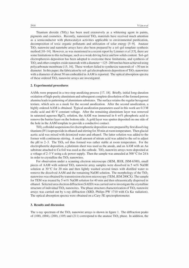
Titanium dioxide (TiO2) has been used extensively as a whitening agent in paints,pigments and cosmetics. Recently, nanosized TiO2 materials have received much attentionas a semiconductor with photocatalyst activities applicable to environmental purification,decomposition of toxic organic pollutants and utilization of solar energy [5–9]. AnataseTiO2 nanowire and nanotube arrays have also been prepared by a sol–gel template synthesismethod [10–14]. However, as was mentioned in a recent report by Limmer et al [15], there aresome limitations to this technique, such as a weak driving force and low solids content. Sol–gelelectrophoresis deposition has been adopted to overcome these limitations, and synthesis ofTiO2 and other complex oxide nanorods with a diameter ∼125–200 nm has been achieved usingpolycarbonate membrane [15, 16]. These workers failed to synthesize nanorods of <50 nm indiameter. In this paper, the fabrication by sol–gel electrophoresis deposition of TiO2 nanowireswith a diameter of about 50 nm embedded in AAM is reported. The optical absorption spectraof these ordered TiO2 nanowire arrays are investigated.
2. Experimental procedures
AAMs were prepared in a two-step anodizing process [17, 18]. Briefly, initial long-durationoxidation of high-purity aluminium and subsequent complete dissolution of the formed porousalumina leads to patterning of aluminium substrates. The surface retains the regular hexagonaltexture, which acts as a mask for the second anodization. After the second anodization, ahighly ordered AAM is obtained. Typical anodization parameters used in this work are 0.3 Moxalic acid and 40 V constant voltage. After the remaining aluminium layer was removedin saturated aqueous HgCl2 solution, the AAM was immersed in 6 wt% phosphoric acid toremove the barrier layer on the bottom side. A gold layer was sputter deposited on one side ofthe hole in the AAM template to provide a conductive contact.
TiO2 colloidal suspensions for electrophoretic deposition were prepared by first dissolvingtitanium (IV) isopropoxide in ethanol and stirring for 30 min at room temperature. Then glacialacetic acid was mixed with deionized water and ethanol. The latter solution was added to theformer with continuous stirring. A small amount of nitrate acid was added to the sol to adjustthe pH to 2–3. The TiO2 sol thus formed was rather stable at room temperature. For theelectrophoretic deposition, a platinum sheet was used as the anode, and an AAM with an Ausubstrate attached to Cu foil was used as the cathode. TiO2 nanowire arrays were deposited ata voltage of 2–5 V using a dc power supply. Then the sample was annealed at 500 ◦C for 24 hin order to crystallize the TiO2 nanowires.
For observation under a scanning electron microscope (SEM, JEOL JSM-6300), smallpieces of AAM with ordered TiO2 nanowire array samples were dissolved in 5 wt% NaOHsolution at 30 ◦C for 20 min and then lightly washed several times with distilled water toremove the dissolved AAM and the remaining NaOH solution. The morphology of the TiO2
nanowires was obtained by transmission electron microscopy (TEM, JEM 200CX). The samplefor TEM was treated by 5 wt% NaOH solution for 40 min and then ultrasonically dispersed inethanol. Selected area electron diffraction (SAED) was carried out to investigate the crystallinestructure of individual TiO2 nanowires. The phase structure characterization of TiO2 nanowirearrays was carried out by x-ray diffraction (XRD, Philips PW 1710 with Cu Kα radiation).The optical absorption spectra were obtained on a Cary-5E spectrophotometer.
3. Results and discussion
The x-ray spectrum of the TiO2 nanowire arrays is shown in figure 1. The diffraction peaksof (100), (004), (200), (105) and (211) correspond to the anatase TiO2 phase. In addition, the

Fabrication and optical properties of TiO2 nanowire arrays 2919
Figure 1. XRD spectrum of the fabricated TiO2 nanowires.
200nm
Figure 2. A typical SEM image of the fabricated TiO2 nanowires.
peak positions and their relative intensities are consistent with the standard powder diffractionpatterns of TiO2, indicating that there is no preferred orientation and that the TiO2 nanowiresare polycrystalline. The broadening of TiO2 peaks is due to the small particle size. Further,no obvious peaks for the amorphous AAM were observed.
Figure 2 shows a typical SEM top image of TiO2 nanowire arrays grown in the AAMtemplate by sol–gel electrophoresis deposition and annealed at 500 ◦C for 24 h. It can beseen that the nanowires are continuous, uniform throughout the entire length of the wires andarranged roughly parallel to one another. The diameter of the TiO2 nanowires is about 50 nm,which is almost equal to the pore size of the template used. Some broken nanowires can beseen, and this can be explained by the differences in thermal expansion coefficients of themembranes and nanowires, distortion of the membranes and the preparation of samples.
The individual TiO2 nanowires were characterized by TEM after the AMM template hadbeen thoroughly dissolved. The TEM image (figure 3) showed that the single TiO2 nanowirewas straight, dense and continuous. The crystalline structure of the individual TiO2 nanowirewas investigated by SAED experiments, and a detailed diffraction pattern (the inset in figure 3)could be observed, indicating that the TiO2 nanowire was anatase polycrystalline structure, ingood agreement with the XRD results.

2920 Y Lin et al
200nm
Figure 3. Typical morphology of one of the TiO2 nanowires; the inset shows the SAED resultstaken from it.
Figure 4. Optical absorption spectra of the TiO2 nanowire arrays in AAM.
By using sol–gel electrophoretic deposition, TiO2 nanowires can be convenientlyfabricated within the nanochannels of the AAM. However, an explanation of the mechanism ofnanowire growth still remains speculative. Sol–gel electrophoretic deposition is a combinationof two processes: electrophoresis and deposition. A dc field causes the charged particles ina suspension to move toward, and deposit on, the oppositely charged electrode [19]. Thesituation becomes more complex due to the presence of the AAM. The size and surface state ofthe charged particles in the suspension are two important factors in determining the processingof electrophoretic deposition. In addition, the precursor concentration, the applied voltage andthe pore diameter of the AAM also have an important influence on the deposition process.Determining the exact nature of the deposition process will require further detailed study.
Optical absorption spectra were obtained on a Cary-5E spectrophotometer at roomtemperature. Figure 4 shows the optical absorption spectra of the blank AAM and theTiO2/AAM assembly system annealed at 500 ◦C. It can be seen that the spectrum of the

Fabrication and optical properties of TiO2 nanowire arrays 2921
Figure 5. (αhν)1/2 versus hν plot for the TiO2 nanowire arrays in AAM.
annealed TiO2/AAM assembly system is quite different from that of the blank AAM. It isknown that the relationship between absorption coefficient α near the absorption edge and theoptical bandgap Eg for indirect interband transitions obeys the following formula [20, 21]:
(αhν)1/2 = A(hν − Eg)
A is the parameter that depends on the interband transition probability, and hν is the energyof incident light. Hence, the optical bandgap for the absorption edge can be obtained byextrapolating the linear portion of the plot (αhν)1/2 versus hν to α = 0. Figure 5 shows(αhν)1/2 versus hν plots for the sample annealed at 500 ◦C. For all samples, the opticalabsorption in the edge region can be well fitted by the relation (αhν)1/2 ∼ hν − Eg, whichshows that TiO2 nanowires embedded in AAM have an indirect bandgap. The bandgap ofTiO2 nanowires in AAM is about 3.35 eV for samples annealed at 500 ◦C. This shows thatthe optical band edge of the TiO2 nanowires embedded in AAM exhibits a marked blue shiftwith respect to that of bulk anatase TiO2 (3.2 eV). There are many reports concerned withquantum size effects in low-dimensional semiconductor systems. It is well known that thesemiconductor nanoparticle energy gap increases with decreasing grain size, which leads toa blue shift of the optical absorption edge and has been observed in many semiconductornanoparticle systems [21–24]. Here the blue shift could also be attributed to the quantum sizeeffect. In figures 4 and 5, a small absorption band is observed around 540 nm (2.3 eV), but theexact origin of this absorption is still unclear.
4. Conclusions
In summary, ordered anatase polycrystalline TiO2 nanowire arrays embedded in AAM wereprepared using sol–gel electrophoretic deposition. The TiO2 nanowires (diameter ∼50 nm)were dense, continuous and uniform throughout the entire length of the wires. A blue shift ofthe optical bandgap of the TiO2/AAM was observed and was mainly attributed to the quantumsize effect.

2922 Y Lin et al
Acknowledgment
This work was supported by the Ministry of Science and Technology of China (grantno G1999064501).
References
[1] Martin C R 1994 Science 266 1961[2] Huezko A 2000 Appl. Phys. A 70 361[3] Brumlik C J and Martin C R 1991 J. Am. Chem. Soc. 113 3174[4] Brumlik C J, Menon V P and Martin C R 1994 J. Mater. Res. 9 1174[5] Linsebigle A L, Lu G Q and Yates J T 1995 Chem. Rev. 95 735[6] Hoffmann M R, Matin S T, Choi W Y and Bahnemann D W 1995 Chem. Rev. 95 69[7] Imai H, Matsuda M, Shimizu K, Hirashima H and Negishi N 2000 J. Mater. Chem. 10 2005[8] Dagan G and Tomkiewics M 1993 J. Phys. Chem. 97 12651[9] Bach U, Lupo D, Comte P, Moser J E, Weissortel F, Salbeck J, Spreitzer H and Gratzel M 1998 Nature 395 583
[10] Lakshmi B B, Dorhout P K and Martin C R 1997 Chem. Mater. 9 857[11] Lakshmi B B, Patrissi C J and Martin C R 1997 Chem. Mater. 9 2254[12] Lei Y, Zhang L D, Meng G W, Li G H, Zhang X Y, Liang C H, Chen W and Wang S X 2001 Appl. Phys. Lett.
78 1125[13] Zhang M, Bando Y and Wada K 2001 J. Mater. Sci. Lett. 20 167[14] Chu S Z, Wada K, Inoue S and Todoroki S 2002 Chem. Mater. 14 266[15] Limmer S J, Seraji S, Forbess M J, Wu Y, Chou T P, Nguyen C and Cao G Z 2001 Adv. Mater. 13 1269[16] Limmer S J, Seraji S, Wu Y, Chou T P, Nguyen C and Cao G Z 2002 Adv. Funct. Mater. 12 59[17] Masuda H and Fukuda K 1995 Science 268 1446[18] Masuda H and Staoh M 1996 Japan. J. Appl. Phys. 2 35 L126[19] Sarkar P and Nicholson P S 1996 J. Am. Ceram. Soc. 79 1987[20] Bassani F and Parravicini G P 1975 Electronic States and Optical Transitions in Solids (New York: Pergamon)
p 149[21] Abe T, Tachibana Y, Uematsu T and Iwamoto M 1995 J. Chem. Soc. Chem. Commun. 1617[22] Yoffe A D 1993 Adv. Phys. 42 173[23] Cormann C, Bahnemann D W and Hoffmann M R 1988 J. Phys. Chem. 92 5196[24] Yuan Z H, Tang C C and Fan S S 2001 Chin. Phys. Lett. 18 1520