
Fabrication and Characterization of a Label Free...
57
Fabrication and Characterization of a Label Free Graphene Field Effect Transistor Biosensor Peter M. Wojcik Department of Physics Oregon State University Corvallis, OR August 16, 2012
-
Upload
truongmien -
Category
Documents
-
view
221 -
download
4
Transcript of Fabrication and Characterization of a Label Free...
Fabrication and Characterization of a Label Free
Graphene Field Effect Transistor Biosensor
Peter M. Wojcik
Department of Physics
Oregon State University
Corvallis, OR
August 16, 2012
i
ABSTRACT
This project addresses the fabrication and characterization of a graphene field
effect transistor (GFET) for use as a biological sensing device. The graphene used in
these experiments was grown via chemical vapor deposition (CVD). The CVD
method is a cost and time effective technique to produce graphene, and can satisfy the
needs for the commercialization of a portable biological sensing device. We
demonstrate a fabrication method for developing a label free aptamer modified CVD
graphene based field effect transistor (FET) biosensor. These devices were used to
detect thrombin protein using a microfluidic mass flow system. The thrombin
biological sensing experiment showed a measureable change in resistance in our
device when thrombin protein was added to the system. The resistance increased after
the addition of a buffer solution suggesting that thrombin protein was bound to the
aptamer modified graphene surface, and was removed by the buffer solution. This
experiment suggests that a label free aptamer modified CVD graphene based FET
biosensing device can be used for accurate protein detection.
ii
PREFACE
This paper was submitted to the Department of Physics at Oregon State
University on August 16, 2012 in partial fulfillment of the requirements for the degree
of Master of Science in Physics. All work presented in this paper, including figures, is
original and should not be copied or reproduced without permission.
When I joined Ethan Minot’s group in January 2012, Ethan initially gave me
the task of fabricating a graphene field effect transistor. After a prototype device was
made I wanted to reproduce similar results from a paper which used an aptamer
modified graphene field effect transistor (GFET) to detect a specific protein without
the use of labels. I began with the development of a new set of devices which
incorporated improved fabrication techniques. These devices were a drastic
improvement to the prototypes and showed us that an aptamer modified GFET
biosensing device may be possible. Grant Saltzgaber joined the project during the
fabrication of the new set of devices and developed a functionalization scheme for the
thrombin aptamer. We eventually found success in detecting thrombin protein using
our devices.
The success of this project has been attributed to many people. I would like to
thank Dr. Ethan Minot for giving me the opportunity to work in his group. His
support and guidance made the scope of this project practical for the amount of time I
had left at Oregon State University. Thank you to Tal Sharf, Tristan DeBorde, and Dr.
Landon Prisbrey for their generous and helpful support. Your patience and knowledge
is inspiring and has been invaluable for the success of this project. Thank you Grant

iii
Saltzgaber for deciding to become a part of this project. This could not have been
done without your assistance and support.
Many people contributed to the work in this paper. Tal Sharf took electrical
measurements of the preliminary devices. Grant Saltzgaber took electrical
measurements of the biosensing devices and performed the thrombin aptamer
functionalization scheme. Former Minot group member, Dr. Matthew Leyden, who
now works for Nanotechnology Biomachines, Inc. grew and supplied the graphene for
the biosensing devices. Jenna Wardini assisted with the growth of the graphene used
in the preliminary devices. Josh Kevek gave support with the growth of graphene
used in the preliminary devices, the graphene transfer process, as well as the device
fabrication process.
Peter M. Wojcik August 16, 2012
Corvallis, OR
iv
TABLE OF CONTENTS
Page
1. Introduction ……………………………………………………………… 1
1.1 Graphene ……………………………………………………….. 1
1.2 Biosensors ……………………………………………………… 3
1.2.1 Graphene Biosensors ………………………………….. 4
1.2.2 Graphene Field Effect Transistor Biosensors ………... 5
1.3 Thrombin Protein ………………………………………………. 7
2. Graphene Characterization Theory ………...……………………………. 8
2.1 Electrical Characterization ……..………………………………. 8
2.1.1 Drude Model for Metals ……………………………... 8
2.1.2 Drude Model for a Semiconducting Sheet …………… 10
2.1.3 Band Structure of Graphene …………………………. 11
2.1.4 Graphene Field Effect Transistors …………………… 12
2.1.5 Graphene Field Effect Transistors as Biosensors ……. 15
2.2 Raman Spectroscopy …………………………………………… 18
2.2.1 The G Band …………………………………………... 19
2.2.2 The D Band …………………………………………... 20
2.2.3 The 2D Band …………………………………………. 21
3. Methods ………………………………………………………………….. 23
3.1 Graphene Growth ……………………………………………..... 23
3.2 Fabrication of Graphene Field Effect Transistors …………….... 24
v
TABLE OF CONTENTS (Continued)
Page
3.2.1 Graphene Transfer Process …………………………... 24
3.2.2 Device Fabrication …………………………………… 26
3.3 Functionalization of Thrombin Aptamer ………………………... 29
3.4 Electrical Measurements and Microfluidics …………………... 30
4. Results and Discussion ………………………………………………….. 32
4.1 Preliminary Devices ……………………………………………... 32
4.1.1 Effects of an Anneal Process ………………………… 33
4.2 Biosensing Devices ……………………………………………... 35
4.2.1 Effects of an Anneal Process ………………………… 36
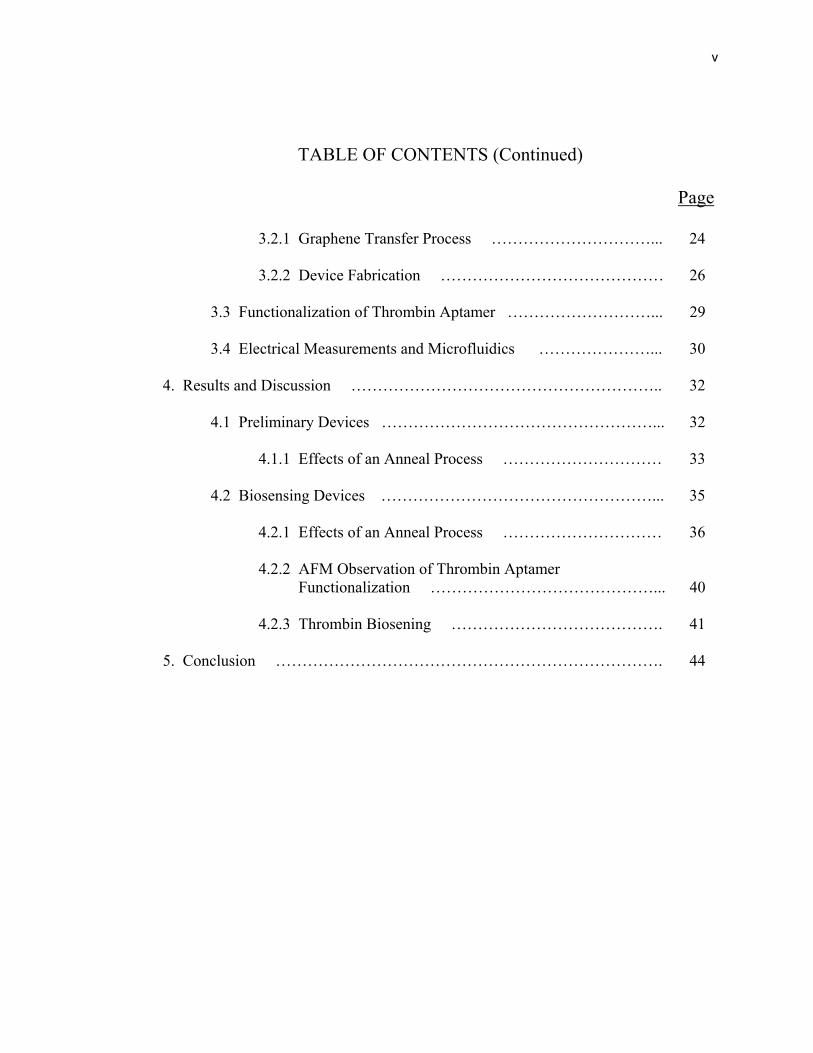
4.2.2 AFM Observation of Thrombin Aptamer Functionalization ……………………………………... 40 4.2.3 Thrombin Biosening …………………………………. 41
5. Conclusion ………………………………………………………………. 44
vi
LIST OF FIGURES
Figure Page
1.1 Hybridization of a sp2 orbital and graphene lattice ………………........... 1
1.2 Drawing of the CVD process ………………………………………. …... 3
1.3 A graphene field effect transistor ……………………………………….. 6
2.1 Energy Diagrams. (a) Insulator, semiconductor, and conductor energy bands. (b) First Brillouin zone of a graphene lattice and 3 dimensional representation of graphene’s conical energy bands plotted as a function of wavevector k …………………… 11 2.2 Schematic of GFET acting as parallel plate capacitor ……………... …... 14
2.3 (a) Schematic of a GFET device. (b) I vs. Vg curve showing regions of hole and electron conduction ……………………………….. 15 2.4 Schematic of liquid-gated GFET device ………………………………... 17
2.5 Raman spectrum of graphene on a Si/SiO2 substrate …………………… 19
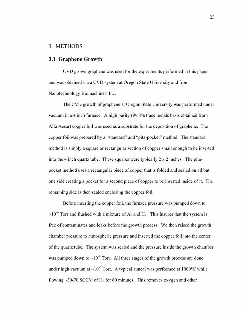
3.1 SEM image of graphene on copper foil ……………………………. …... 24
3.2 Graphene transfer process …………………….………………………… 26 3.3 Device fabrication process for biosensing devices ……………………... 28
3.4 A model of graphene, PBASE, thrombin aptamer and thrombin protein ……………………………………………………….. 30 3.5 Microfluidic experimental setup ……………………………………….. 31
4.1 Electrical characteristics of a preliminary GFET device in open air (a) and in a PBS buffer (b) ………………………………........ 33 4.2 Electrical characteristics of a preliminary GFET device in open air before anneal (a) and in a liquid environment after an anneal (b) …………………………………………………….... 34
vii
LIST OF FIGURES (Continued)
Figure Page
4.3 Electrical characteristics of a biosensing GFET device in open air (a) and in a PBS buffer (b) ………………………………...... 35 4.4 (a) AFM image of graphene channel in GFET before anneal and (b) AFM image of graphene channel in GFET after anneal …………………………………………………………… 37 4.5 (a) Raman spectra of graphene channel in GFET device before and after an anneal. (b) The G and 2D band shifts resulting from the anneal process ……………………………… 38 4.6 (a) AFM image of bare graphene channel in GFET and (b) AFM image of aptamer modified graphene channel in GFET ……………………………………………………………… 40 4.7 (a) I vs. Vlg curve of an aptamer modified GFET device in a MES buffer . (b) Current vs. time for the aptamer modified GFET device ……………………………………………….…...…… 42
1
1. INTRODUCTION
1.1 Graphene
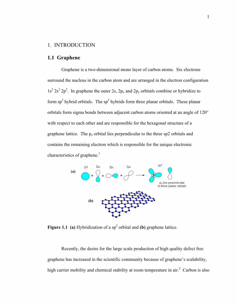
Graphene is a two-dimensional mono layer of carbon atoms. Six electrons
surround the nucleus in the carbon atom and are arranged in the electron configuration
1s2 2s2 2p2. In graphene the outer 2s, 2px and 2py orbitals combine or hybridize to
form sp2 hybrid orbitals. The sp2 hybrids form three planar orbitals. These planar
orbitals form sigma bonds between adjacent carbon atoms oriented at an angle of 120°
with respect to each other and are responsible for the hexagonal structure of a
graphene lattice. The pz orbital lies perpendicular to the three sp2 orbitals and
contains the remaining electron which is responsible for the unique electronic
characteristics of graphene.1
Figure 1.1 (a) Hybridization of a sp2 orbital and (b) graphene lattice.
Recently, the desire for the large scale production of high quality defect free
graphene has increased in the scientific community because of graphene’s scalability,
high carrier mobility and chemical stability at room temperature in air.2 Carbon is also
2
one of the most abundant elements on earth which makes graphene cost effective and
plentiful.
In 2004, a group at the University of Manchester was able to produce single
layer graphene using a technique called mechanical exfoliation which entails the
repeated pealing of pyrolytic graphite.3 Mechanical exfoliation is a reliable method
for producing high quality defect free graphene, however it can only cover very small
areas3 and is therefore not suitable for the large scale production of graphene. There
are several other methods for producing graphene.4 A process that is cost and time
effective and also able to produce large scale defect free graphene is desired to take
advantage of carbon’s abundance and graphene’s unique electrical properties.
Chemical vapor deposition (CVD) is a cost and time effective method for
producing high quality graphene in large quantities. A typical CVD process for
graphene is performed under vacuum and uses heat to break apart the atoms in a
gaseous hydrocarbon such as methane. The remaining carbon atoms then align
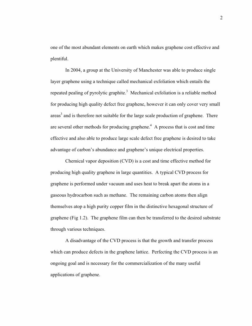
themselves atop a high purity copper film in the distinctive hexagonal structure of
graphene (Fig 1.2). The graphene film can then be transferred to the desired substrate
through various techniques.
A disadvantage of the CVD process is that the growth and transfer process
which can produce defects in the graphene lattice. Perfecting the CVD process is an
ongoing goal and is necessary for the commercialization of the many useful
applications of graphene.
Figure 1.2
Gr
semicondu
ability to m
transmittan
conductive
properties
biological
1.2 Bios
A b
molecules
biosensor.
glucose lev
antibodies
fueled by t
2 Drawing o
aphene trans
uctor devices
maintain per
nce which m
e electrodes
are also pre
sensors.8
sensors
biosensor is
. A blood gl
It is an acc
vels. Other
,10 and DNA
their valuabl
of the CVD p
sistors are a
s in integrate
rformance lo
makes it a po
such as indi
senting new
a device tha
lucose moni
urate and inv
types of bio
A.11 The mot
le applicatio
process. Th
promising c
ed circuits5 d
w temperatu
ssible altern
ium tin oxide
w prospects a
at is capable
itor is an exa
valuable too
logical senso
tivation to cr
ons in gene a
e orange sub
andidate to r
due to their h
ures.6 Graph
native to conv
e.7 Graphen
s electrical b
of detecting
ample of a co
ol for diabeti
ors are used
reate accura
analysis,11 de
bstrate is cop
replace tradi
high carrier m
hene exhibits
ventional tra
e’s extraord
based chemi
g specific bio
ommercially
ics who need
to detect pro
ate biosensin
etection of bi
pper foil.
itional silico
mobility3 an
s a high optic
ansparent
inary electri
cal and
ological
y available
d to monitor
otein,9
g devices is
iological wa
3
on
nd
cal
ical
their
arfare
4
agents,11 and the detection of potentially life threatening diseases like prostate
cancer.12 In gene analysis, the detection of genetic mutations can allow medical
professionals to identify diseases even before any symptoms appear.11
Biosensors can be simplified into two categories, label and non-label based.
Label based technologies chemically modify a biological molecule with a fluorescent
tag that can be seen with a fluorescent microscope, however this method requires a
lengthy labeling process and expensive detection equipment.13 Label free technologies
do not require any tagging to identify specific molecules and are ideal for quick and
accurate diagnosis. Surface Plasmon resonance,14 carbon nanotube (CNT),15
graphene,10 and silicon nanowire16 biological sensors are examples of label free
technologies that are currently under development.
The early detection of certain diseases such as prostate cancer is imperative to
increase a patient’s likely hood of survival. Label free technologies are able to satisfy
the need for a timely method of biological detection by providing real-time, accurate,
specific detection of biological diseases.10,15,17
1.2.1 Graphene Biosensors
A point-of-care (POC) biological sensor is a technology that has recently
received a lot of attention because of their ability to process several biological markers
simultaneously.18 POC systems will also allow technology and information to be
available to a much wider population, which in the past has only been accessible to
leading cancer centers.18 Biosensors which incorporate nanomaterials such as CNTs,
5
nanowires and graphene are able to satisfy the needs of a highly accurate and portable
POC biological sensor. Graphene is of particular interest for use in POC biosensors
because of its nanoscale dimensions, large surface area, and high carrier mobility.
There are many graphene biosensing technologies currently being investigated.
A group at Fuzhou University has shown that graphene oxide (GO) is a potential
platform for the selective detection of DNA and proteins, and compared to CNTs,
GO’s low cost and large production scales make it a promising candidate for
biosensing devices.19 Recently, a graphene based fluorescence resonance energy
transfer (FRET) sensor was developed and reported to have detected thrombin to
limits as low as 31.3 pM, which is two orders of magnitude lower than CNT based
fluorescence sensors.9 Other biosensing technologies incorporate graphene into a field
effect transistor for use as a biological sensing device.10,20,21
1.2.2 Graphene Field Effect Transistor Biosensors
A field effect transistor (FET) is a voltage controlled device which is capable
of varying a current across a semiconducting channel by the application of an electric
field. In a graphene field effect transistor (GFET) the graphene sheet acts as the
semiconducting channel between two metal source and drain electrodes which lie atop
an electrical insulator such as SiO2. When charged biological molecules bind on the
surface of the semiconducting graphene sheet in the GFET there is a measureable
change in resistance. The GFET device is able to act as a real-time all electronic
biosensor based on this detection principle.
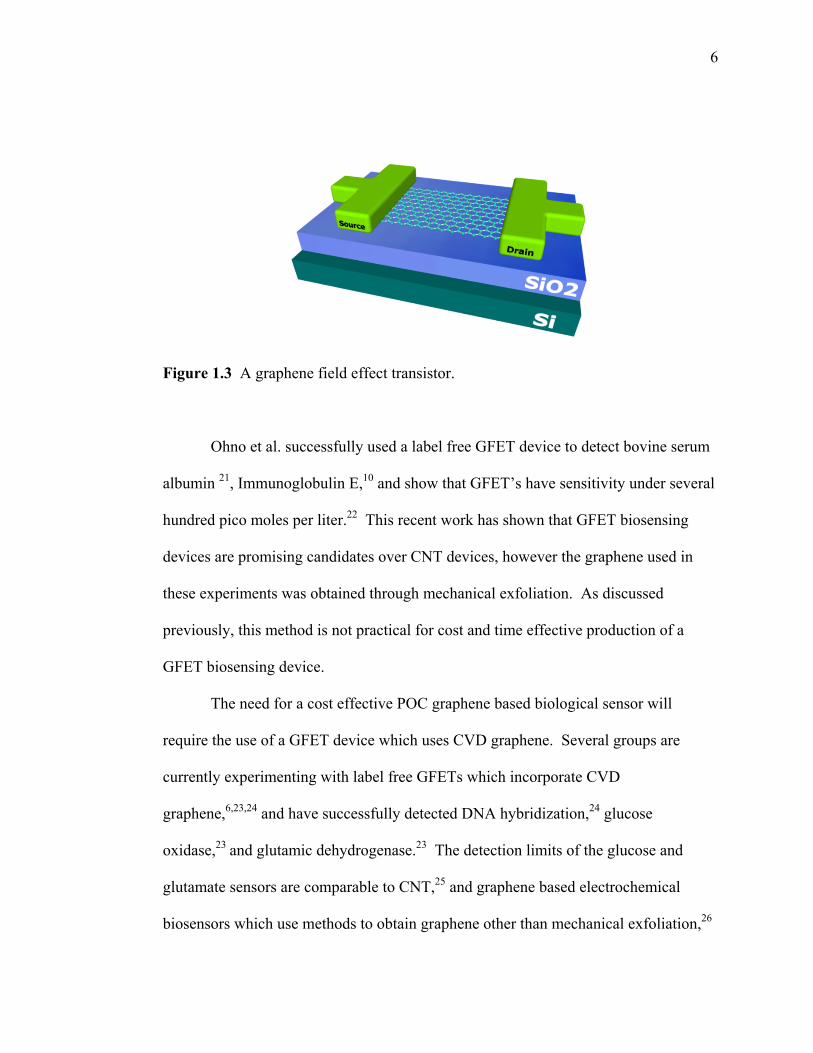
6
Figure 1.3 A graphene field effect transistor.
Ohno et al. successfully used a label free GFET device to detect bovine serum
albumin 21, Immunoglobulin E,10 and show that GFET’s have sensitivity under several
hundred pico moles per liter.22 This recent work has shown that GFET biosensing
devices are promising candidates over CNT devices, however the graphene used in
these experiments was obtained through mechanical exfoliation. As discussed
previously, this method is not practical for cost and time effective production of a
GFET biosensing device.
The need for a cost effective POC graphene based biological sensor will
require the use of a GFET device which uses CVD graphene. Several groups are
currently experimenting with label free GFETs which incorporate CVD
graphene,6,23,24 and have successfully detected DNA hybridization,24 glucose
oxidase,23 and glutamic dehydrogenase.23 The detection limits of the glucose and
glutamate sensors are comparable to CNT,25 and graphene based electrochemical
biosensors which use methods to obtain graphene other than mechanical exfoliation,26
7
however are still inferior to nanowire,27 and CNT28 based electrochemical biosensors.
The recent attention and work dedicated to the large scale production of high quality
graphene will likely show that graphene is a practical and superior alternative to other
nanomaterials which are incorporated into biosensors.
1.3 Thrombin Protein
Thrombin protein is produced by the body and has an important role in the
blood clotting or coagulation process,29 and the regulation of tumor growth.30
The selective and sensitive detection of thrombin may be useful in surgical procedures
and cardiovascular disease therapy.29 There have been many efforts to produce a
sensitive biological sensor for the detection of thrombin.9,31 In the past, thrombin has
been optically detected using a fluorescence based tag,31 which we have previously
discussed as a slow and costly method for detection. In this paper we will address the
feasibility of a CVD graphene based label free FET biosensor to accurately detect
thrombin.
8
2. GRAPHENE CHARACTERIZATION THEORY
2.1 Electrical Characterization
2.1.1 Drude Model for Metals
Three years after the discovery of the electron by J.J. Thomsen in 1897, P.
Drude constructed a theory of electrical and thermal conduction which applied the
kinetic theory of gases to metals.32 The kinetic theory applied to metals assumes that
electrons behave classically, i.e. they can be treated like solid spheres which travel in
straight line paths until they collide with each other or imperfections in the solid.
Drude’s model can used to describe and quantify some of graphene’s unique electrical
characteristics.
Ohm’s Law, which can be explained using Drude’s model, states that the
potential across a conducting wire is proportional to the current flowing through
the wire, or
(2.1)
where is the resistance of the conducting wire, and is measured in Ohms or
equivalently Volts/Ampere. The resistance is independent of the magnitude of the
current or potential drop but depends on the wire’s dimensions.
If we assume that the current is distributed evenly over the cross sectional
area of our conducting wire, then the current density is ⁄ . If there exists an
electrical field , it will exert forces on the moving charges and hence there should be
some functional relationship between and . This relationship can be expressed as
9
(2.2)
where is a proportionality constant called the resistivity. This constant eliminates
the dependence on the dimensions of the wire and is a measure of how well a
conductor is able to oppose the flow of an electrical current. Equation (2.2) is
typically expressed in terms of the inverse of the resistivity, or the conductivity as
(2.3)
This relationship is the macroscopic equivalent to Ohm’s law for a linear isotropic
homogeneous conductor and is often referred to as the microscopic form of Ohm’s
law.33
If we again consider the case where there exists an electrical field , there will
be a mean velocity directed opposite to the applied field. This average velocity is
called the drift velocity and is related to the electric field by
(2.4)
where is called the electron mobility and tells us how fast electrons can travel
through a conductor when an applied electric field exerts a force on them.
Let us consider number of electrons per unit volume all traveling at velocity
through a cross sectional area . The electrons will move a distance in time
and electrons will pass through the cross sectional area . The charge
passing through in time will be and the current density is
(2.5)
Using equations (2.3), (2.4), and (2.5) we can now relate the conductivity to mobility
by

10
(2.6)
2.1.2 Drude Model for a Semiconducting Sheet
Note that the equation for conductance is only valid when the conductivity is
only due to electrons. In a p-type semiconductor the conductivity is due to holes, in
which case the conductance is given by
(2.7)
where is the hole density and is the hole mobility. In a semiconductor which
conducts by electrons and holes the conductivity is
(2.8)
Another useful quantity for describing the electrical properties of graphene is
sheet resistance, which is a measure of resistance of very thin films which are uniform
in thickness. Let’s consider a current flowing uniformly through a wire conductor of
length . The potential across that length will be , and from eq. (2.2) gives
/ . Therefore the resistance and resistivity are related by
(2.9)
If we now consider the cross sectional area to have some width and thickness
then (2.9) becomes
(2.10)
where / and is called the sheet resistance.
11
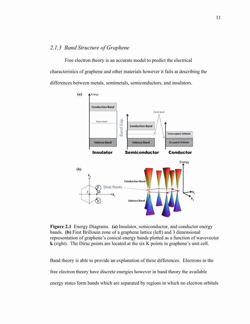
2.1.3 Band Structure of Graphene
Free electron theory is an accurate model to predict the electrical
characteristics of graphene and other materials however it fails at describing the
differences between metals, semimetals, semiconductors, and insulators.
Figure 2.1 Energy Diagrams. (a) Insulator, semiconductor, and conductor energy bands. (b) First Brillouin zone of a graphene lattice (left) and 3 dimensional representation of graphene’s conical energy bands plotted as a function of wavevector k (right). The Dirac points are located at the six K points in graphene’s unit cell.
Band theory is able to provide an explanation of these differences. Electrons in the
free electron theory have discrete energies however in band theory the available
energy states form bands which are separated by regions in which no electron orbitals
12
exist. These forbidden regions are called band gaps. In insulators, the band gap
between the valence and conduction energy bands is very large. In conductors, the
valence and conduction bands overlap, and in semiconductors there is a small band
gap between the valence and conduction band which allows for unique thermal and
optical excitations. The band structure of graphene is very unique because its valence
and conduction band are symmetrical shaped cones which connect at a Dirac point.
This point subsequently means that graphene does not contain a band gap.
2.1.4 Graphene Field Effect Transistors
The Fermi energy level is an important consideration when discussing band
theory and GFET devices. The Fermi level quantifies the highest occupied electron
energy level at absolute zero temperature. The Fermi level can lie inside a band gap
(where no energy levels exist). In this case the Fermi energy, , is used in the Fermi-
Dirac distribution to calculate the probability that nearby energy levels are thermally
populated.
1/ 1
(2.11)
The quantity is Boltzmann’s constant, is the absolute temperature, and is the
energy level of the particle. For 0, in the limit 0, the argument in the
exponential becomes minus infinity and makes the exponential term zero. Hence the
probability, , that nearby energy levels less than the Fermi energy are thermally
populated is 1 at 0. For 0, in the limit 0, the argument in the
13
exponential becomes infinity and makes the exponential term infinite. Hence the
probability, , that nearby energy levels greater than the Fermi energy are
thermally populated is zero at 0.
In an intrinsic semiconductor like undoped silicon, the Fermi level is halfway
between the valence and conduction bands. This means that at absolute zero
temperature there are no electrons in the conduction band however at finite
temperatures some electrons have energies higher than the Fermi level and can reach
the conduction band. The Fermi level in a GFET device can essentially be shifted by
applying a bias across one of the electrodes and the back gate.
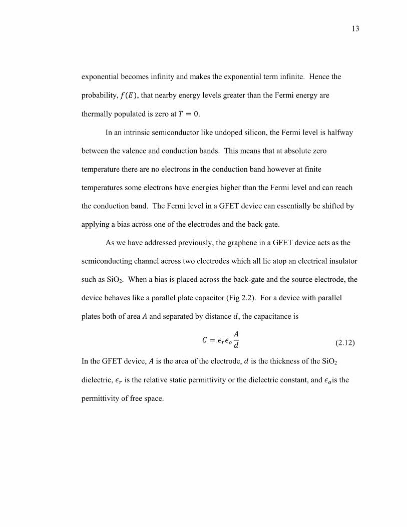
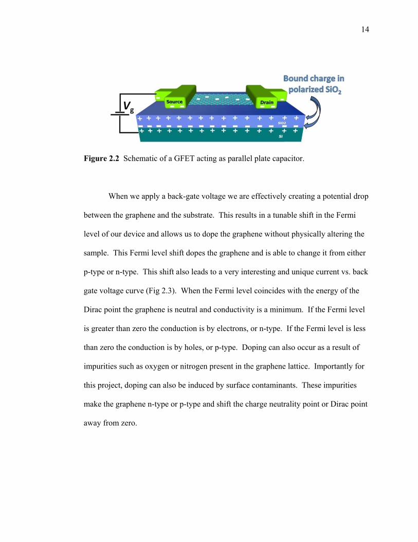
As we have addressed previously, the graphene in a GFET device acts as the
semiconducting channel across two electrodes which all lie atop an electrical insulator
such as SiO2. When a bias is placed across the back-gate and the source electrode, the
device behaves like a parallel plate capacitor (Fig 2.2). For a device with parallel
plates both of area and separated by distance , the capacitance is
(2.12)
In the GFET device, is the area of the electrode, is the thickness of the SiO2
dielectric, is the relative static permittivity or the dielectric constant, and is the
permittivity of free space.
14
Figure 2.2 Schematic of a GFET acting as parallel plate capacitor.
When we apply a back-gate voltage we are effectively creating a potential drop
between the graphene and the substrate. This results in a tunable shift in the Fermi
level of our device and allows us to dope the graphene without physically altering the
sample. This Fermi level shift dopes the graphene and is able to change it from either
p-type or n-type. This shift also leads to a very interesting and unique current vs. back
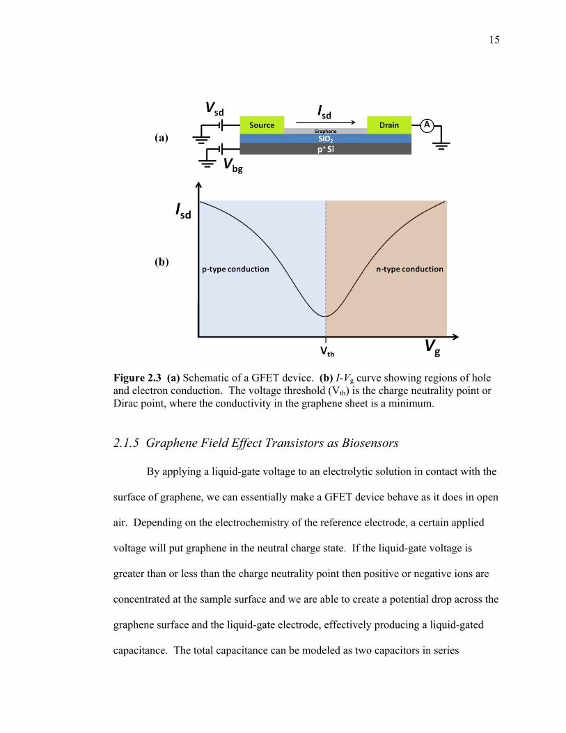
gate voltage curve (Fig 2.3). When the Fermi level coincides with the energy of the
Dirac point the graphene is neutral and conductivity is a minimum. If the Fermi level
is greater than zero the conduction is by electrons, or n-type. If the Fermi level is less
than zero the conduction is by holes, or p-type. Doping can also occur as a result of
impurities such as oxygen or nitrogen present in the graphene lattice. Importantly for
this project, doping can also be induced by surface contaminants. These impurities
make the graphene n-type or p-type and shift the charge neutrality point or Dirac point
away from zero.
15
Figure 2.3 (a) Schematic of a GFET device. (b) I-Vg curve showing regions of hole and electron conduction. The voltage threshold (Vth) is the charge neutrality point or Dirac point, where the conductivity in the graphene sheet is a minimum.
2.1.5 Graphene Field Effect Transistors as Biosensors
By applying a liquid-gate voltage to an electrolytic solution in contact with the
surface of graphene, we can essentially make a GFET device behave as it does in open
air. Depending on the electrochemistry of the reference electrode, a certain applied
voltage will put graphene in the neutral charge state. If the liquid-gate voltage is
greater than or less than the charge neutrality point then positive or negative ions are
concentrated at the sample surface and we are able to create a potential drop across the
graphene surface and the liquid-gate electrode, effectively producing a liquid-gated
capacitance. The total capacitance can be modeled as two capacitors in series
16
1 1 1
(2.13)
where is the quantum capacitance and is the geometrical capacitance. The
geometrical capacitance is given by eq. (2.12) where is a new quantity called the
Debye length. The quantum capacitance is related to the Fermi level shift and
subsequently, the potential drop across this capacitance controls the Fermi level
shift.34
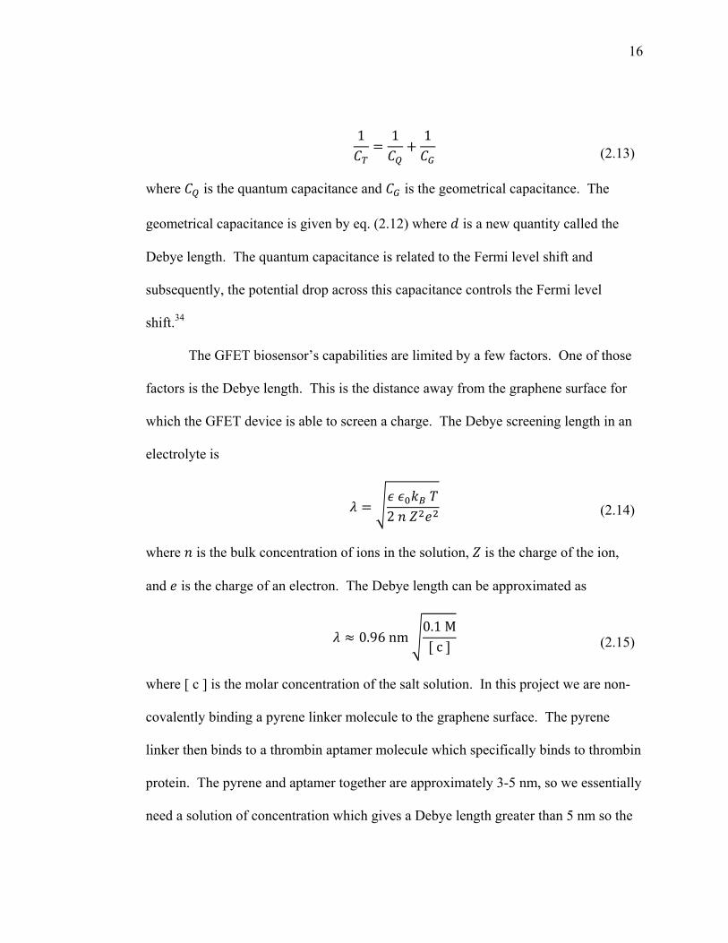
The GFET biosensor’s capabilities are limited by a few factors. One of those
factors is the Debye length. This is the distance away from the graphene surface for
which the GFET device is able to screen a charge. The Debye screening length in an
electrolyte is
2 (2.14)
where is the bulk concentration of ions in the solution, is the charge of the ion,
and is the charge of an electron. The Debye length can be approximated as
0.96 nm0.1 M
c (2.15)
where [ c ] is the molar concentration of the salt solution. In this project we are non-
covalently binding a pyrene linker molecule to the graphene surface. The pyrene
linker then binds to a thrombin aptamer molecule which specifically binds to thrombin
protein. The pyrene and aptamer together are approximately 3-5 nm, so we essentially
need a solution of concentration which gives a Debye length greater than 5 nm so the
17
GFET device can screen and detect a charge when the thrombin protein binds to the
aptamer.
Figure 2.4 Schematic of a liquid-gated GFET device. Positive (or negative depending on the applied liquid-gate voltage) ions near the surface of the graphene make up the Debye layer.
The GFET biosensing device is highly sensitive to any fluctuations in local
charge distributions. It has been shown that charge trapping in GFET devices can be
detrimental to its performance.35 Charge trapping occurs when charges migrate into
the dielectric substrate. This results in a loss of mobility in the graphene sheet and
creates unwanted low frequency noise. Recently, Heller et al. have shown that for low
carrier densities the noise in a liquid-gated GFET device is dominated by charge
fluctuations near the graphene sheet and that the power of the charge noise in these
devices scales inversely with the device area and number of graphene layers.36
Another factor that limits a GFET biosensing device is Faradaic currents.
These currents are created by the reduction or oxidation of molecules at the liquid-
metal interface. The result is a charge transfer occurring at the electrode surface
creating unwanted currents in the device. A measurement of these currents in the
18
window of the liquid-gate voltage is necessary to make sure that they are not dominant
over currents associated with the graphene sheet. In general, Faradaic currents should
be less than 1 nA. For the experiment presented in this paper, Faradaic currents of 1
nA are approximately 3 orders of magnitude smaller than currents in the graphene, and
therefore negligible. Faradaic currents can be alleviated by passivation, which entails
coating the top of the electrodes with a layer of oxide to reduce the interaction
between the electrode surface and the solution.
2.2 Raman Spectroscopy
The carbon atoms in a graphene lattice can be modeled as masses on springs
where the mass is the mass of the carbon atom and the spring is the bond between
atoms. When an incident photon strikes the graphene lattice an inelastic collision
occurs and energy is lost from the photon and transferred into the vibration of the
lattice. This amount of energy lost into the vibration of the graphene lattice can be
quantified by calculating the energy difference between the incident and reflected
photon. This process is called Raman spectroscopy and can tell us specific
information about the structure of a graphene lattice by simply observing the
energy(ies) of reflected photons.
A Raman spectral analysis of a graphene lattice can reveal information about
the number of graphene layers present,37 defects in the lattice,38 the amount by which
the graphene may be doped,39 and the angle at which double stacked graphene is
19
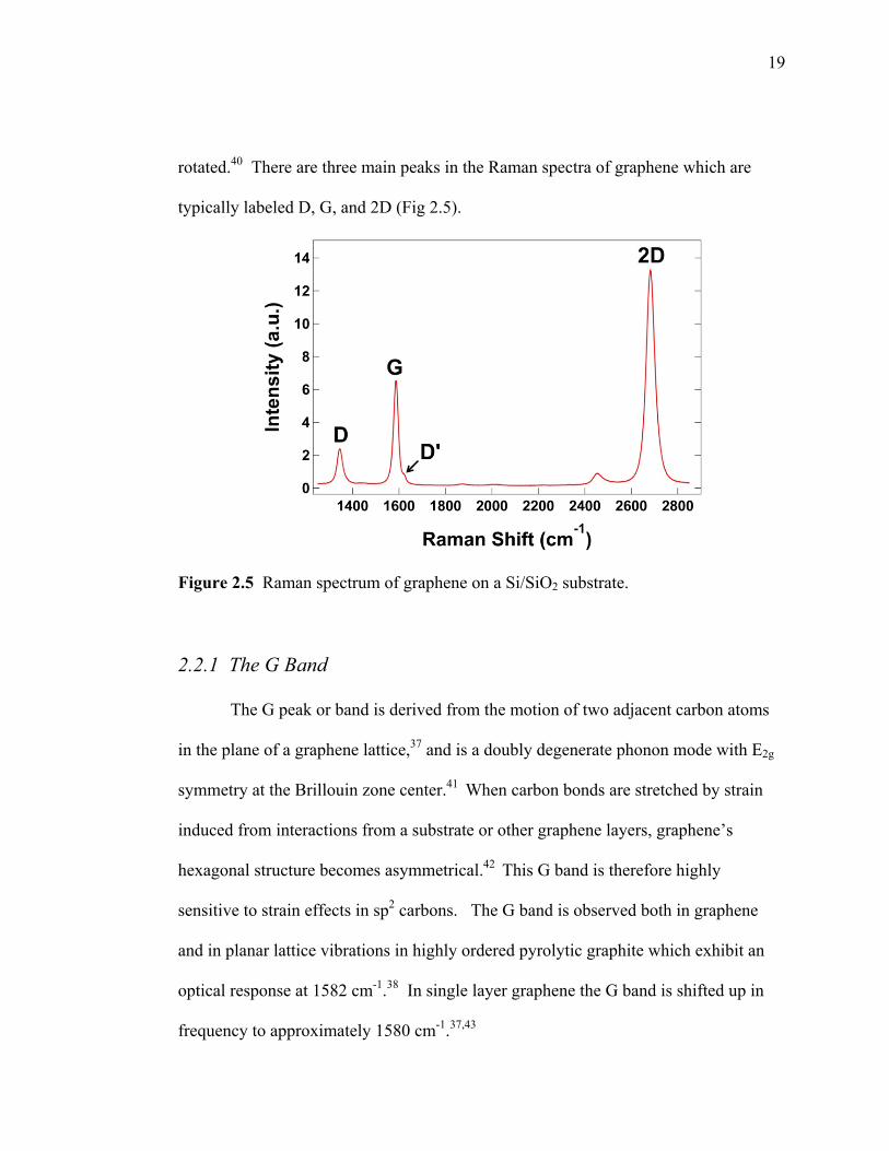
rotated.40 There are three main peaks in the Raman spectra of graphene which are
typically labeled D, G, and 2D (Fig 2.5).
Figure 2.5 Raman spectrum of graphene on a Si/SiO2 substrate.
2.2.1 The G Band
The G peak or band is derived from the motion of two adjacent carbon atoms
in the plane of a graphene lattice,37 and is a doubly degenerate phonon mode with E2g
symmetry at the Brillouin zone center.41 When carbon bonds are stretched by strain
induced from interactions from a substrate or other graphene layers, graphene’s
hexagonal structure becomes asymmetrical.42 This G band is therefore highly
sensitive to strain effects in sp2 carbons. The G band is observed both in graphene
and in planar lattice vibrations in highly ordered pyrolytic graphite which exhibit an
optical response at 1582 cm-1.38 In single layer graphene the G band is shifted up in
frequency to approximately 1580 cm-1.37,43
20
Recent studies using GFET devices have shown that Raman spectroscopy is a
valuable tool to characterize doping levels by observing the frequency and width of
the G band.44-46 These studies induced electron and hole doping in graphene by
varying the gate voltage and observing the corresponding Raman spectra for each gate
voltage. Shifting the Fermi energy level from induced doping results in a change in
the equilibrium lattice parameter, and the excess charge results in an expansion or
contraction of the graphene lattice.45 As we discussed previously, the G band is
sensitive to any strain induced on sp2 carbons and subsequently results in a shift in
frequency and width.45 Other groups have discovered similar shifts in frequency of the
G band due to doping from aromatic molecules,47 and from doping along the edges of
graphene.39
2.2.2 The D Band
The edges of graphene typically contain defects and are characterized by a D
band in the Raman spectrum around approximately 1350 cm-1.43 Disorder induced
Raman features can also appear as a second band typically labeled D’ and occur
around approximately 1620 cm-1.41 D and D’ bands have been observed on graphene
lattices after inducing defects by the deposition of SiO2,48 and also by bombardment of
the lattice with electrons,49 and Ar+ ions.50 The causes of D and D’ bands are
theorized to be from vacancies, dislocated or dangling bonds in the graphene lattice,48
and from certain crystallographic orientations of the graphene edges.51 Raman
21
spectroscopy has been valuable in characterizing defect and edge features in graphene
as well as graphitic materials in general.41,50,52
In 1970, Tuinstra and Koenig quantified the evolution of disorder in crystalline
sp2 clusters by using a ratio of the intensities of the D and G bands.53 They found that
the ratios of the intensities of the D and G bands follow the relationship
(2.16)
where is the crystalline size, and is a proportionality constant which depends
on the excitation laser wavelength.53 A new model proposed by Lucchese et al. uses
the ratio ⁄ to quantify the density of defects, or the average distance, between
defects in graphene.50 This model shows that the ratio ⁄ increases with increasing
up to approximately 4 nm then decreases exponentially for > 4 nm.50 This
behavior is explained by the competition between two disorder mechanisms, and their
model can be used to quantify the relative importance of each mechanism.50
2.2.3 The 2D Band
Similar to the G band, the 2D band is present in all types of sp2 carbon
materials and displays a strong feature in the Raman spectra around approximately
2700 cm-1.37,38,43 The D and 2D bands are activated by a double resonance (DR)
process which involves the coupling of two phonons with opposite wavevectors.37,54
This DR process results in a dispersive relationship which consequently causes the 2D
band to be dependent on perturbations to the electronic and/or phonon structure of
22
graphene and exhibit a strong frequency dependence on the excitation energy from the
laser.37,54,55
Recent work has shown that the 2D band can be used to identify the number of
layers present in AB stacked graphene.43,54 As the number of layers increases the DR
processes increase until the shape of the 2D band eventually converges to that of bulk
graphite which results in two peaks.54 It should be noted that this method for
identifying the number of layers is only well established for samples made from
mechanical exfoliation of HOPG which predominately have AB stacking, however
this is not necessarily the case for graphene obtained from other methods which may
have layers that are rotationally random with respect to one another.40,54
A common misconception is to assume that a large ratio between the
intensities of the 2D and G bands is a good method to distinguish between single or
multilayer graphene. Recent reports have observed the Raman spectra for SiO2 doped
single layer graphene,48 double-stacked rotated graphene,40 and single layer graphene
that has been doped via a gate voltage,45 which show that the ⁄ ratio and the
position of the G peak should not be used to estimate the number of graphene layers.
This is contrary to what was previously suggested by Gupta et al.,56 and Graf et al.57
The 2D band, like the G band, is sensitive to doping,45,46,58 however the bands
show different dependencies on doping levels.45,46 These dependencies show that the
ratio ⁄ is a strong function of doping induced by a gate voltage and is therefore
an important parameter to estimate doping densities in graphene.45
23
3. METHODS
3.1 Graphene Growth
CVD grown graphene was used for the experiments performed in this paper
and was obtained via a CVD system at Oregon State University and from
Nanotechnology Biomachines, Inc.
The CVD growth of graphene at Oregon State University was performed under
vacuum in a 4 inch furnace. A high purity (99.8% trace metals basis obtained from
Alfa Aesar) copper foil was used as a substrate for the deposition of graphene. The
copper foil was prepared by a “standard” and “pita-pocket” method. The standard
method is simply a square or rectangular section of copper small enough to be inserted
into the 4 inch quartz tube. These squares were typically 2 x 2 inches. The pita-
pocket method uses a rectangular piece of copper that is folded and sealed on all but
one side creating a pocket for a second piece of copper to be inserted inside of it. The
remaining side is then sealed enclosing the copper foil.
Before inserting the copper foil, the furnace pressure was pumped down to
~10-6 Torr and flushed with a mixture of Ar and H2. This insures that the system is
free of contaminates and leaks before the growth process. We then raised the growth
chamber pressure to atmospheric pressure and inserted the copper foil into the center
of the quartz tube. The system was sealed and the pressure inside the growth chamber
was pumped down to ~10-6 Torr. All three stages of the growth process are done
under high vacuum at ~10-6 Torr. A typical anneal was performed at 1000°C while
flowing ~30-70 SCCM of H2 for 60 minutes. This removes oxygen and other
contamina
The growt
SCCM Me
the same g
Figure 3.1Nanotechn
3.2 Fabr
3.2.1 Gr
Aft
side of the
methacryla
copper etc
hours. Th
top layer o
ates from the
th stage was
ethane for 20
growth gases
1 SEM imagnology Biom
rication of
raphene Tr
fter the grow
e copper was
ate (PMMA)
chant (type C
e etchant rem
of graphene a
e growth cha
performed a
0 minutes. T
s.
ge of graphemachines, Inc
f Graphen
ransfer Pro
wth process th
s spun coated
) in a solutio
CE-200) bath
moves the bo
and PMMA.
amber and co
at 1000°C w
The furnace
ne on coppec.
ne Field Ef
ocess
he copper fo
d at 4000 rpm
on of Anisole
h with the PM
ottom layer o
. A diluted h
opper foil be
while flowing
was then co
er foil. This
ffect Tran
oil was cut in
m for 1 minu
e. The samp
MMA side fa
of graphene
hydrochloric
efore the grow
g ~50-70 SCC
oled to 200°
graphene wa
nsistors
nto 2 x 2 cm
ute with 2%
ples were the
facing upwar
and copper
c acid bath w
wth process
CM of H2 an
°C while flow
as obtained f
squares. On
polymethyl
en placed int
rd for at leas
foil, leaving
was also used
24
.
nd 2
wing
from
ne
to a
t 12
g the
d as
25
an etchant. Graphene samples were placed a bath consisting of DI water, HCl, and
H2O2 with a 45:5:1 ratio for 12 hours. This etchant resulted in tearing a majority of
the graphene samples. A shorter time period, or a more diluted concentration of HCl
and H2O2 might result in less tears.
After etching, the samples were transferred to 3 separate deionized (DI) water
baths for approximately 30 minutes each, then to a final DI water bath for at least 12
hours. A fresh silicon wafer was used to transfer the samples. After each transfer the
silicon wafer was cleaned with acetone, isopropyl alcohol, DI water, and then dried
with ultra high purity N2. All glassware used in the transfer process was cleaned using
the same process.
The silicon substrates used in the biosensing experiments were obtained from
WRS Materials and were p-doped with a 500 nm top layer of thermal oxide. The
Si/SiO2 wafers were cut into 2 x 2 cm squares, large enough to accommodate the
metal electrode pattern. The Si/SiO2 wafers were cleaned with acetone, isopropyl
alcohol, DI water, and then dried with ultra high purity N2 before the transfer process.
The graphene with PMMA was then transferred to the Si/SiO2 wafer. The wafer was
dried from the center of the graphene outward, using low pressure ultra high purity N2
to aid in the adhesion of the graphene to the substrate. The samples were placed in a 1
inch furnace in open air at 30°C for 4 hours before the removal of PMMA to ensure
that the graphene was properly adhered to the substrate. PMMA was removed in the
same 1 inch furnace in open air at 350°C for 4 hours.
26
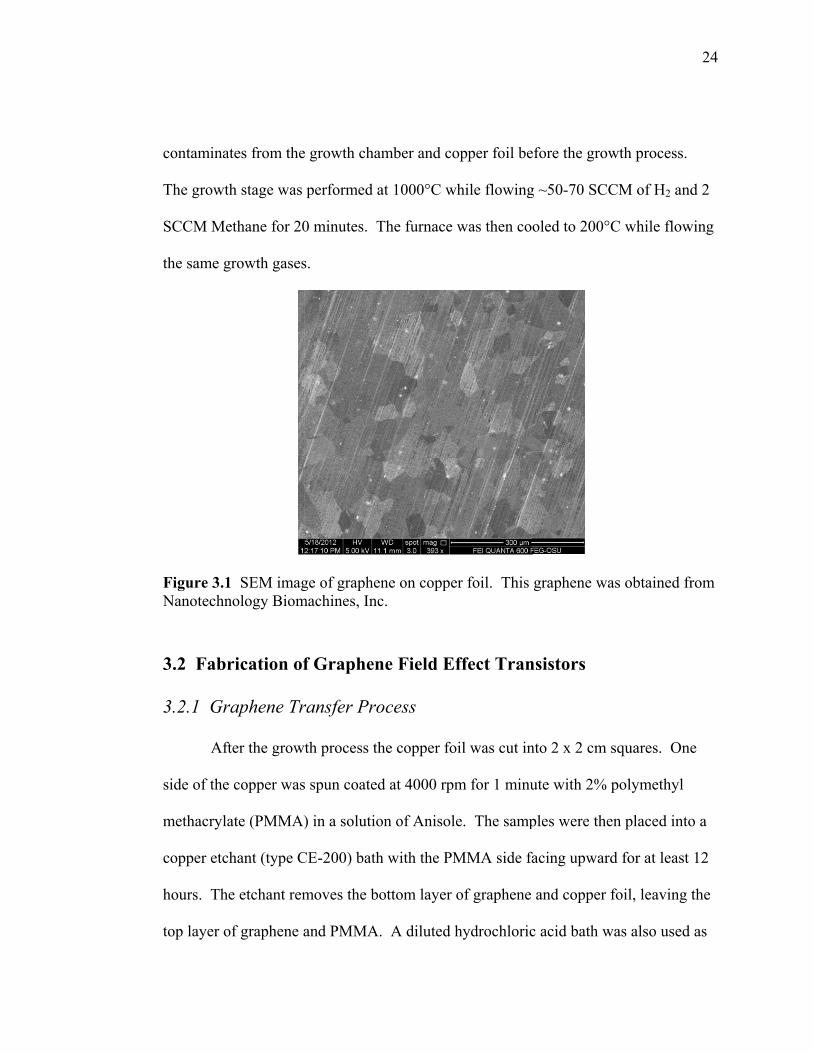
Figure 3.2 Graphene transfer process. (a) Graphene is grown via CVD on copper foil. (b) PMMA is spun on top of graphene. (c) Copper foil is removed with an etchant bath. (d) Graphene with PMMA is transferred to Si/SiO2 substrate. (e) PMMA is removed.
3.2.2 Device Fabrication
The scale of the devices required the use of alignment marks to ensure that
graphene would be properly aligned across the electrode gaps. Alignment marks were
pattered onto the Si/SiO2 substrate using photolithography and a metal deposition.
The samples were spun coated with LOR3A at 4000 rpm for 45 seconds then baked on
a hot plate for 4 minutes at 190°C. The LOR3A under layer aids in the process of
metal lift off. S1813 photoresist was then spun coated at 4000 rpm for 30 seconds and
baked on a hot plate for 90 seconds at 115°C. A contact aligner was used along with
an appropriate alignment mark mask to expose the samples for 4.5 seconds. The
samples were developed in AZ-726 for 90 seconds and rinsed in a short DI bath. 20
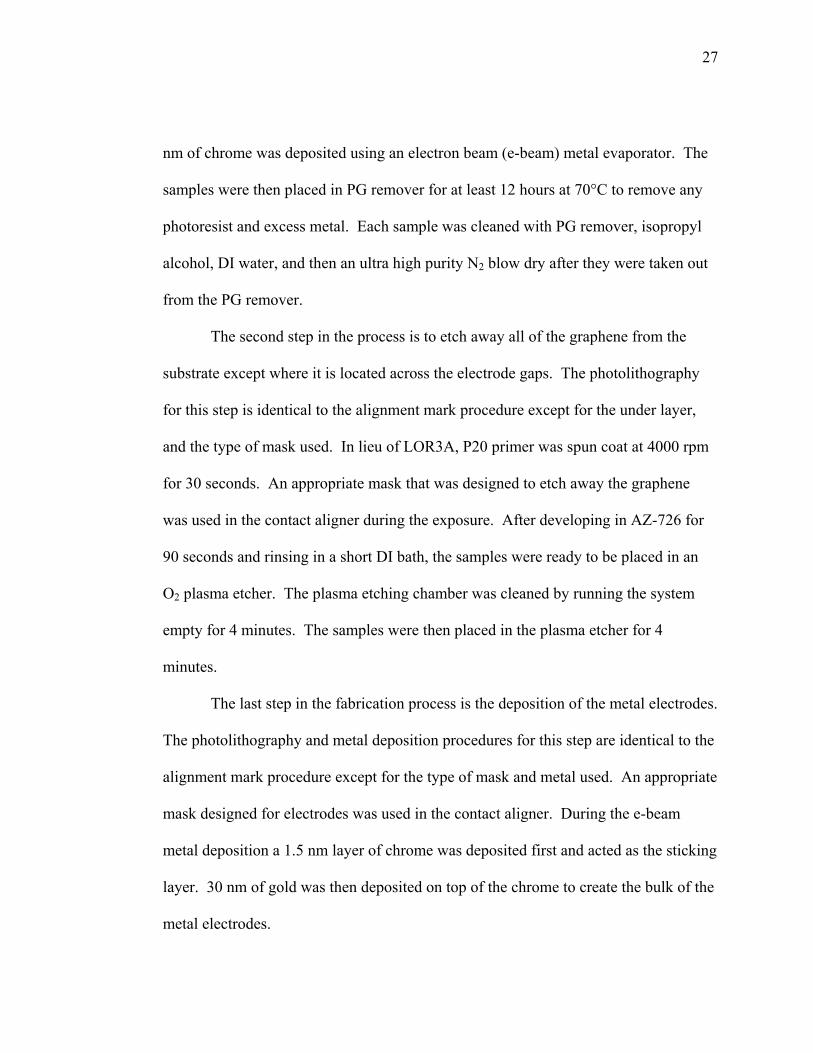
27
nm of chrome was deposited using an electron beam (e-beam) metal evaporator. The
samples were then placed in PG remover for at least 12 hours at 70°C to remove any
photoresist and excess metal. Each sample was cleaned with PG remover, isopropyl
alcohol, DI water, and then an ultra high purity N2 blow dry after they were taken out
from the PG remover.
The second step in the process is to etch away all of the graphene from the
substrate except where it is located across the electrode gaps. The photolithography
for this step is identical to the alignment mark procedure except for the under layer,
and the type of mask used. In lieu of LOR3A, P20 primer was spun coat at 4000 rpm
for 30 seconds. An appropriate mask that was designed to etch away the graphene
was used in the contact aligner during the exposure. After developing in AZ-726 for
90 seconds and rinsing in a short DI bath, the samples were ready to be placed in an
O2 plasma etcher. The plasma etching chamber was cleaned by running the system
empty for 4 minutes. The samples were then placed in the plasma etcher for 4
minutes.
The last step in the fabrication process is the deposition of the metal electrodes.
The photolithography and metal deposition procedures for this step are identical to the
alignment mark procedure except for the type of mask and metal used. An appropriate
mask designed for electrodes was used in the contact aligner. During the e-beam
metal deposition a 1.5 nm layer of chrome was deposited first and acted as the sticking
layer. 30 nm of gold was then deposited on top of the chrome to create the bulk of the
metal electrodes.
28
Figure 3.3 Device fabrication process for biosensing devices. (a) Photoresist is spun onto Si/SiO2 substrate. (b) The photoresist is patterned for alignment marks and developed. (c) Chrome alignment marks are deposited via e-beam metal evaporation and remaining metal and photoresist are stripped. (d) Graphene is transferred to Si/SiO2 substrate, PMMA is removed, and photoresist is spun on top of graphene. (e) Photoresist is patterned and developed for graphene etching. (f) Graphene is removed via O2 plasma etching, and remaining photoresist is stripped. (g) Photoresist is spun onto sample. (h) Photoresist is patterned for electrodes and developed. (i) Gold electrodes are deposited via e-beam metal evaporation and excess metal and photoresist are stripped.
A preliminary and secondary set of devices were fabricated for the experiments
performed in this paper. The secondary sets of devices were used in the biosensing
experiments. In the preliminary set, alignment marks were patterned after graphene
was transferred to the Si/SiO2 substrate. The graphene used for the preliminary
devices was grown via CVD at Oregon State University, and the graphene width
across the 4 μm electrode gaps was 32 μm. For the biosensing devices, contamination
of the graphene surface through an extra photolithography step was avoided by
patterning alignment marks on the Si/SiO2 substrate before the graphene was
transferred. The graphene used for the biosensing devices was obtained from
29
Nanotechnology Biomachines, Inc., and the graphene width across the 4 μm electrode
gaps was reduced to 3 μm.
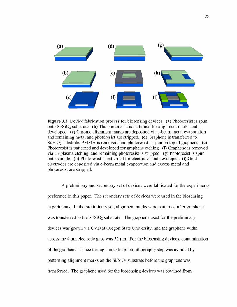
3.3 Functionalization of Thrombin Aptamer
Amine reactive 1-pyrenebutanoic acid succinimidyl ester (PBASE) was
obtained from Invitrogen and acted as the linker molecule between the graphene
surface and thrombin aptamer. PBASE has been used in the past for both carbon
nanotube15 and graphene10 functionalization. The PBASE non-covalently binds to the
graphene surface via stacking. GFET devices were immersed in a methanol solution
of 5mM PBASE for 1 hour at room temperature to achieve functionalization with the
graphene surface. The devices were rinsed with methanol then immersed in a 20 mM
2-morpholinoethanesulfonic acid (MES) solution with1nM thrombin aptamer for 12
hours at room temperature. The custom synthesized thrombin aptamer DNA
oligonucleotide was obtained from Integrated DNA Technologies and the base
sequence was 5’-/5Amino C6/GGT TGG TGT GGT TGG-3’. The oligonucleotide
came synthesized with an amine group which reacts with the amine-reactive PBASE
molecule. A final rinse with 20 mM MES solution at room temperature was
performed to remove any reactive groups that may have remained on the graphene
surface. The thrombin protein from human plasma was obtained from Sigma-Aldrich.
30
Figure 3.4 PBASE (green) on graphene sheet, thrombin aptamer (middle) and cartoon rendering of thrombin protein (top).
3.4 Electrical Measurements and Microfluidics
Electrical measurements were performed inside a Faraday cage for the
reduction of noise. All probe needles were insulated and had their shielding grounded
to a common point. This common point was also the location for all other ground
connections. The source-drain voltage was supplied by a Stanford Research Systems
(SR570) pre-amplifier. The source-drain voltage for all measurements performed in
this paper was 25 mV. The current was measured with the SR570 current pre-
amplifier which converted the current to a voltage and output the signal to a National
Instruments DAQ (NI USB 6251) analog to digital converter. Liquid and back-gate
voltages were supplied with a Yokogawa GS200 DC voltage/current source.
31
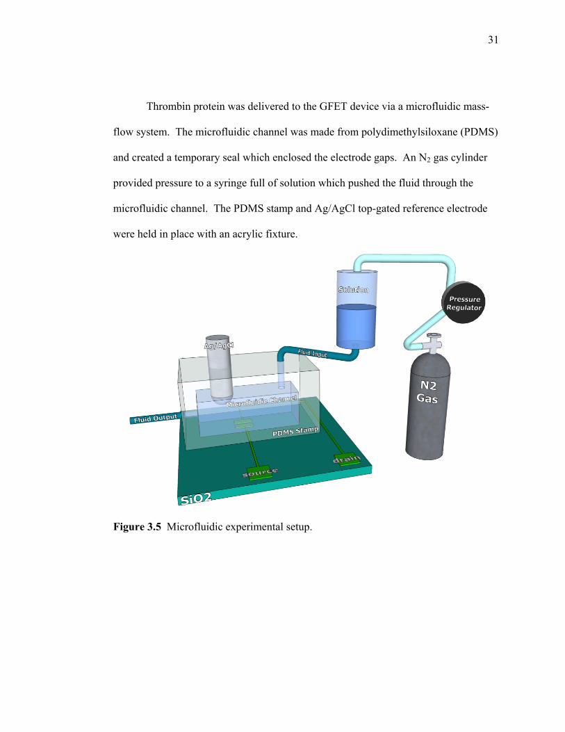
Thrombin protein was delivered to the GFET device via a microfluidic mass-
flow system. The microfluidic channel was made from polydimethylsiloxane (PDMS)
and created a temporary seal which enclosed the electrode gaps. An N2 gas cylinder
provided pressure to a syringe full of solution which pushed the fluid through the
microfluidic channel. The PDMS stamp and Ag/AgCl top-gated reference electrode
were held in place with an acrylic fixture.
Figure 3.5 Microfluidic experimental setup.
32
4. RESULTS AND DISCUSSION
4.1 Preliminary Devices
Electrical measurements were taken on the preliminary set of devices to
observe their electrical characteristics in both open air and liquid environments, and to
determine if they were suitable for a biosensing experiment.
All measurements taken in open air were back gated. Initial electrical
measurements showed a back gate response in open air. The charge neutrality point
was beyond Vbg = +200 V, which suggested that the device was heavily p-doped. The
anomaly in the transistor curve shown in Fig 4.1 (a) around the range of 180-200 V
was believed to be an effect of the voltage amplifier and not related to the device’s
electrical characteristics. The open air gate response also shows evidence of
hysteresis. Hysteresis phenomena are thought to be the result of charge trapping,59 or
altering the surface dipole moment near graphene which may occur from tape
residues,60 atmospheric water,60,61 or e-beam resist.59 In later AFM scans we observed
a residue on the surface of our graphene which was believed to be from the
photolithography processes. The hysteresis we observed may therefore be a result of
that residue, or from charge trapping near the graphene.
To measure devices in liquid, a PDMS stamp was fitted to the GFET device as
described in section 3.4. The device was flushed with ethanol, and then a PBS buffer
(pH 7) was added to observe the liquid gated response. Faradaic currents were
measured and were less than 1 nA. The Faradaic currents dictate the range of the
liquid gate voltage. Beyond these ranges, Faradaic currents are greater than 1 nA and
33
can no longer be neglected in comparison to the current in the graphene channel. The
charge neutrality point was outside the range of the liquid gate voltage, suggesting that
our device was heavily p-doped. Compared to the open air measurements, there was
higher conductance, and a larger on/off ratio (data not shown).
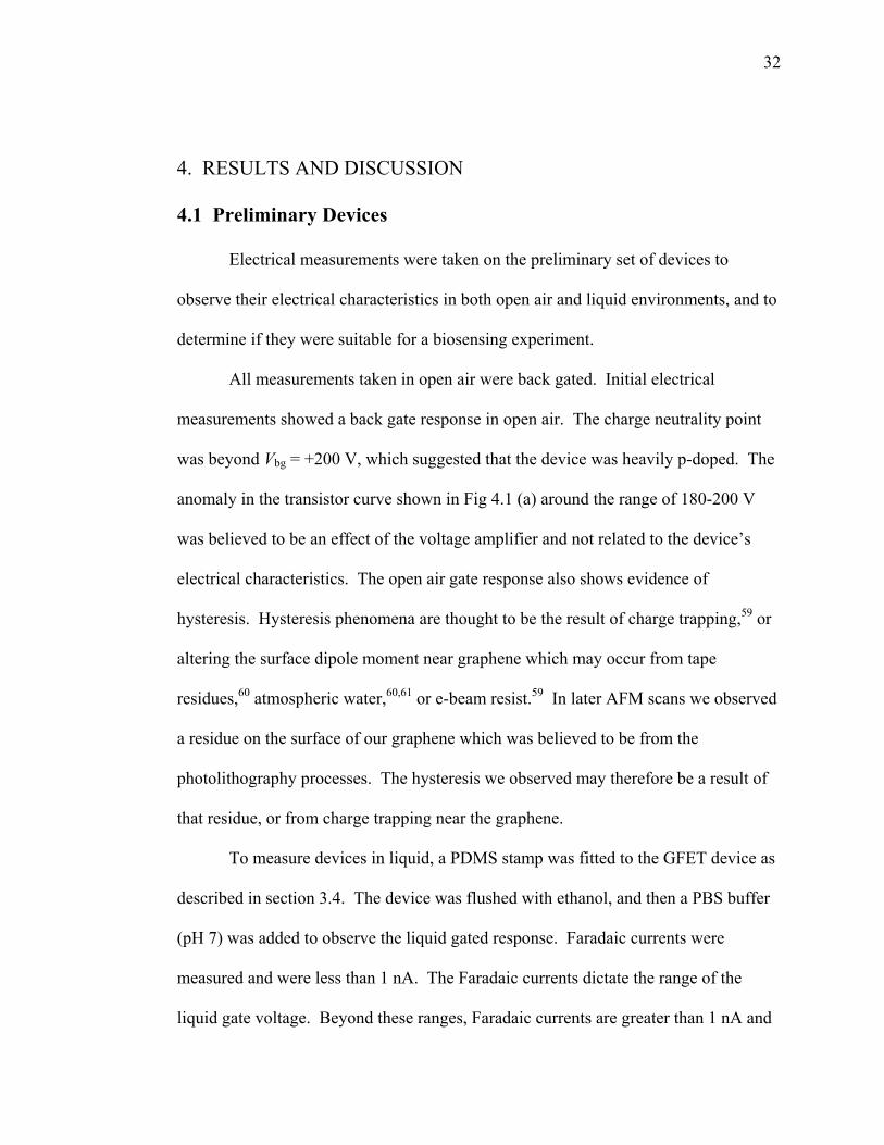
Figure 4.1 Electrical characteristics of a preliminary GFET device in open air (a) and in a PBS buffer (b). The blue arrows indicate the direction the gate voltage was swept.
4.1.1 Effects of an Anneal Process
A preliminary GFET device was annealed to clean the graphene surface and
observe any changes in its electrical characteristics. The GFET was annealed at 500°C
while flowing 1 SLM Ar and 0.45 SLM H2 for 20 minutes. A gate response was
observed in open air before the anneal (Fig 4.2a). We observed a lower on/off ratio
compared to the open air gate response of the GFET in the previous section. The
charge neutrality point was outside the range of the gate voltage, suggesting that the
device was heavily p-doped. After the anneal, the device was fitted with a PDMS
stamp, flushed with ethanol, and immersed in a PBS buffer (pH 7). Faradaic currents
34
were measured and were less than 1 nA. The GFET device exhibited a gate response,
however, the charge neutrality point was beyond the range of the liquid gate voltage.
The on/off ratio of the liquid gated annealed device was much smaller compared to the
open air electrical response.
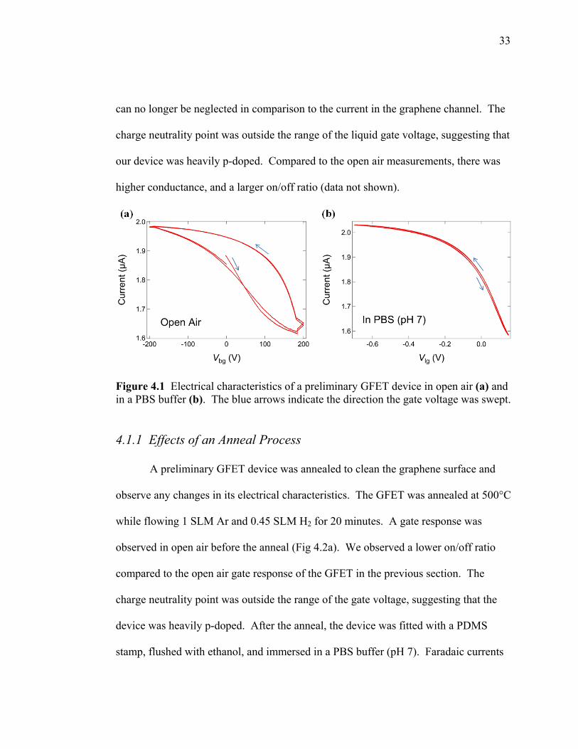
Figure 4.2 Electrical characteristics of a preliminary GFET device in open air before anneal (a) and in a liquid environment after an anneal (b).
Based on these results it was difficult to say whether an anneal improved the
electrical characteristics of our devices. An important factor in a biosensing
experiment is to the see the shift in the charge neutrality point before and after a
molecule has bound to the surface of the graphene sheet. Therefore, it was
disappointing that we could not access the charge neutrality point in our preliminary
devices.
We were unable to see a charge neutrality point in a liquid environment in all
the experiments performed on our preliminary devices. Therefore, we decided to
make a second set of devices, revise the photolithography process and modify one step
35
in the process. In this second set of devices, the alignment marks were deposited on
the Si/SiO2 substrate before transferring the graphene. This limited the graphene’s
exposure to photolithography steps. Photoresist only contacts the graphene twice
instead of three times, thus limiting the amount of residue that may contaminate the
graphene surface.
4.2 Biosensing Devices
Electrical measurements were taken on the second set of GFET devices to
observe their electrical characteristics and determine if they were suitable for
biosensing experiments. The GFET device was back gated and showed a response
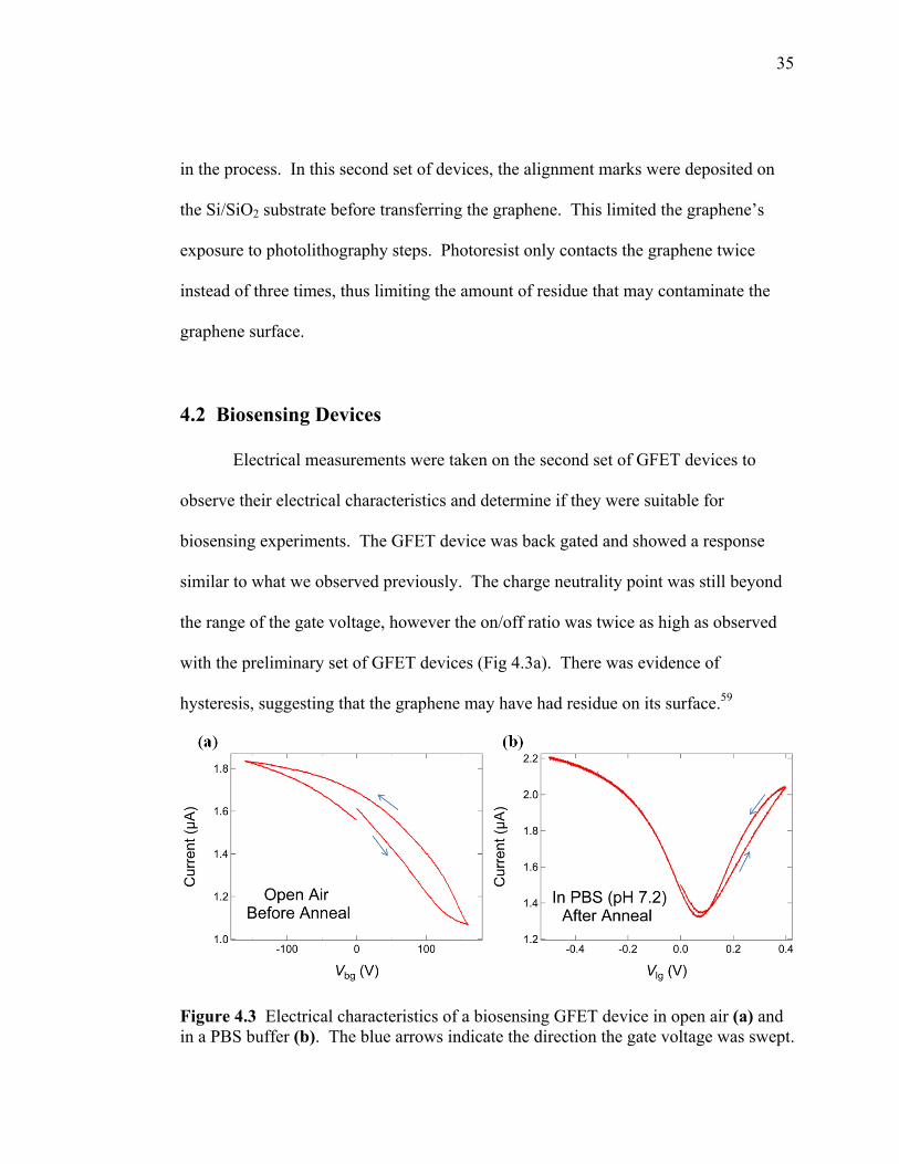
similar to what we observed previously. The charge neutrality point was still beyond
the range of the gate voltage, however the on/off ratio was twice as high as observed
with the preliminary set of GFET devices (Fig 4.3a). There was evidence of
hysteresis, suggesting that the graphene may have had residue on its surface.59
Figure 4.3 Electrical characteristics of a biosensing GFET device in open air (a) and in a PBS buffer (b). The blue arrows indicate the direction the gate voltage was swept.
36
The device was annealed before it was immersed in a liquid environment. The
GFET was annealed at 400°C while flowing 0.85 SLM Ar and 0.95 SLM H2 for 1
hour. The GFET was then fitted with a PDMS stamp, flushed with ethanol, and
immersed in a PBS buffer (pH 7.2). Faradaic currents were measured and were less
than 1 nA. The liquid gated GFET device exhibited a gate response with a charge
neutrality point within the liquid-gate voltage range. This data suggested that these
devices were suitable for a biosensing experiment.
4.2.1 Effects of an Anneal Process
A fresh device from the same batch was chosen to attempt a thrombin
biosensing experiment. First, the GFET was annealed at 400°C while flowing 0.85
SLM Ar and 0.95 SLM H2 for 1 hour. The intention of this anneal was to improve the
thrombin aptamer functionalization scheme by cleaning the surface of the graphene.
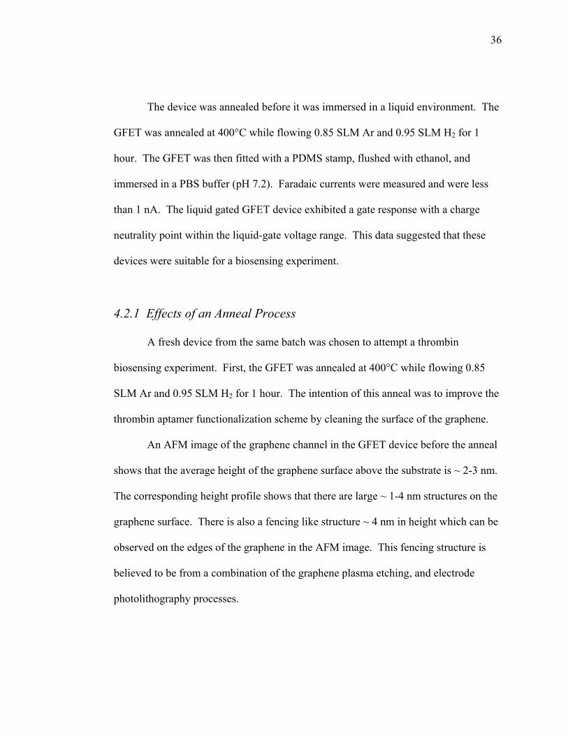
An AFM image of the graphene channel in the GFET device before the anneal
shows that the average height of the graphene surface above the substrate is ~ 2-3 nm.
The corresponding height profile shows that there are large ~ 1-4 nm structures on the
graphene surface. There is also a fencing like structure ~ 4 nm in height which can be
observed on the edges of the graphene in the AFM image. This fencing structure is
believed to be from a combination of the graphene plasma etching, and electrode
photolithography processes.
37
Figure 4.4 (a) AFM image of graphene channel in GFET before anneal and corresponding height profile marked by blue line. (b) AFM image of graphene channel in GFET after anneal and corresponding height profile marked by blue line. The electrodes are located in the top and bottom ~ 0.5 μm portions of both AFM images. A color map of the height range is located at the left of each AFM image.
The AFM image of the graphene channel after the anneal shows a drastic
improvement in height characteristics. A height profile was taken at the approximate
location of the height profile from the pre-anneal AFM image and shows that the
average height of the graphene surface above the substrate after the anneal was
reduced to ~ 0.5 nm. The height profile also shows that the fencing structure
surrounding the graphene edges was reduced by as much as 3 nm. Comparing the two
38
AFM images we can see that there was a thin coat of residue on the graphene surface
before the anneal, and that most of this residue was removed after the anneal.
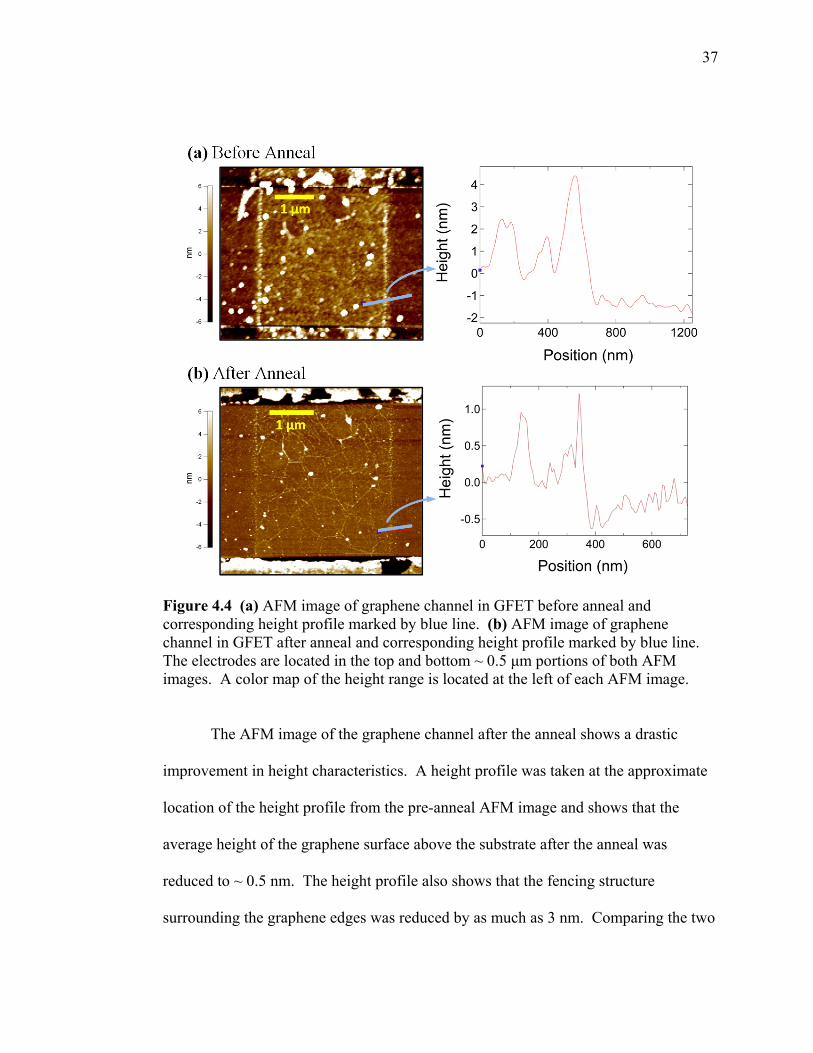
Raman spectra were attained for the graphene channel in the GFET device
before and after the anneal. A 532 nm laser with an excitation energy of 2.33 eV was
used to record the spectra in ambient light conditions. The laser was positioned in the
same spot in the graphene channel before and after the anneal. The Raman spectra
suggest that the graphene in the GFET channel is most likely double or multi layer.40,52
Figure 4.5 (a) Raman spectra of graphene channel in GFET device before (blue) and after (red) an anneal. (b) The G and 2D band shifts resulting from the anneal process.
39
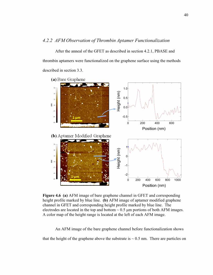
Recent studies performed on electrochemically top gated GFETs have shown
that the positions of the G and 2D bands, as well as their FWHM exhibit clear
dependencies on hole and electron doping.45 The Raman spectra for the graphene
channel in our GFET device show that there was a significant shift in the positions of
the G and 2D bands. The G peak position in our Raman spectra increases from 1588
cm-1 to 1597 cm-1, and the FWHM decreases in line width from 26 to 24 after the
anneal process. This shift in the position and stiffening of the G peak are
characteristic of doping effects,45 however cannot be used alone to distinguish between
electron and hole doping.45
As experimentally determined by Das et al., the position of the 2D peak
decreases for an increasing electron concentration and therefore allows the 2D peak
position to distinguish between electron and hole doping.45 The 2D peak position in
our Raman spectra increases from 2684 cm-1 to 2690 cm-1, suggesting that the electron
concentration decreased, resulting in a device that was more p-type after the anneal.
The ratio of the 2D and G peak intensities also show a clear dependence on
electron concentration.45 This ratio decreases from 0.88 to 0.61 after the anneal and
suggests that the anneal was responsible for changing the doping level of the device. 45
The ratios of the D and G peak intensities only varied slightly from 0.30 to 0.37,
suggesting that no significant defects were introduced into the graphene lattice during
the anneal process.50
40
4.2.2 AFM Observation of Thrombin Aptamer Functionalization
After the anneal of the GFET as described in section 4.2.1, PBASE and
thrombin aptamers were functionalized on the graphene surface using the methods
described in section 3.3.
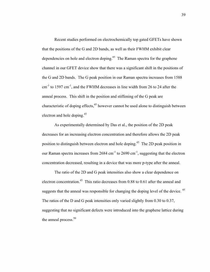
Figure 4.6 (a) AFM image of bare graphene channel in GFET and corresponding height profile marked by blue line. (b) AFM image of aptamer modified graphene channel in GFET and corresponding height profile marked by blue line. The electrodes are located in the top and bottom ~ 0.5 μm portions of both AFM images. A color map of the height range is located at the left of each AFM image.
An AFM image of the bare graphene channel before functionalization shows
that the height of the graphene above the substrate is ~ 0.5 nm. There are particles on
41
the graphene sheet which are present in both the AFM image and height profile,
however the average height of the graphene surface is ~ 0.5 nm. After
functionalization of the PBASE and thrombin aptamer the height profile of the
graphene surface increased to ~ 3 nm, suggesting that the thrombin aptamer was bound
to the PBASE on the graphene surface. The AFM image of the aptamer modified
graphene shows that some thrombin aptamer and other particles were introduced to the
left and right of the graphene channel on the bare substrate. This is most likely a result
of the functionalization process contaminating the surface.
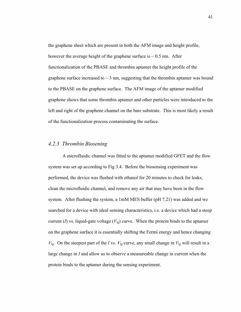
4.2.3 Thrombin Biosening
A microfluidic channel was fitted to the aptamer modified GFET and the flow
system was set up according to Fig 3.4. Before the biosensing experiment was
performed, the device was flushed with ethanol for 20 minutes to check for leaks,
clean the microfluidic channel, and remove any air that may have been in the flow
system. After flushing the system, a 1mM MES buffer (pH 7.21) was added and we
searched for a device with ideal sensing characteristics, i.e. a device which had a steep
current (I) vs. liquid-gate voltage (Vlg) curve. When the protein binds to the aptamer
on the graphene surface it is essentially shifting the Fermi energy and hence changing
Vlg. On the steepest part of the I vs. Vlg curve, any small change in Vlg will result in a
large change in I and allow us to observe a measureable change in current when the
protein binds to the aptamer during the sensing experiment.
42
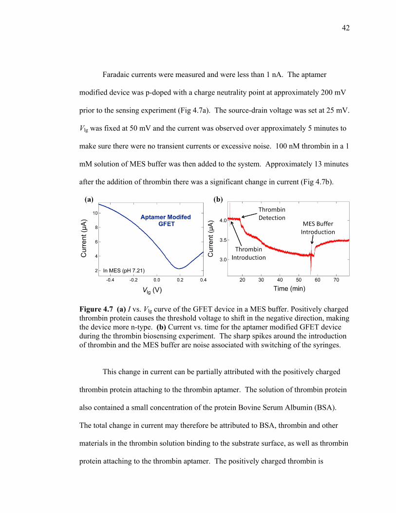
Faradaic currents were measured and were less than 1 nA. The aptamer
modified device was p-doped with a charge neutrality point at approximately 200 mV
prior to the sensing experiment (Fig 4.7a). The source-drain voltage was set at 25 mV.
Vlg was fixed at 50 mV and the current was observed over approximately 5 minutes to
make sure there were no transient currents or excessive noise. 100 nM thrombin in a 1
mM solution of MES buffer was then added to the system. Approximately 13 minutes
after the addition of thrombin there was a significant change in current (Fig 4.7b).
Figure 4.7 (a) I vs. Vlg curve of the GFET device in a MES buffer. Positively charged thrombin protein causes the threshold voltage to shift in the negative direction, making the device more n-type. (b) Current vs. time for the aptamer modified GFET device during the thrombin biosensing experiment. The sharp spikes around the introduction of thrombin and the MES buffer are noise associated with switching of the syringes.
This change in current can be partially attributed with the positively charged
thrombin protein attaching to the thrombin aptamer. The solution of thrombin protein
also contained a small concentration of the protein Bovine Serum Albumin (BSA).
The total change in current may therefore be attributed to BSA, thrombin and other
materials in the thrombin solution binding to the substrate surface, as well as thrombin
protein attaching to the thrombin aptamer. The positively charged thrombin is
43
expected to repel positive carriers from the p-type graphene, thereby reducing the
current in the channel.
Immediately after the detection event there was a sharp decrease in current
which eventually tapered off after approximately 5 minutes. This sharp decrease in
current can be associated with the rapid delivery of thrombin protein to the bare
aptamer modified GFET device. After the binding sites began to be filled, fewer
vacant sites on the aptamer modified graphene surface were available and the rate of
binding slowed. At approximately 55 minutes the device was near saturation, i.e.
there were no more binding sites available for the thrombin protein. A 1 nM MES
buffer was then added to the system. The introduction of the MES buffer caused a
sharp increase in current which can be associated with thrombin protein being
removed from the aptamer modified graphene surface. The signal stabilizes again at
approximately 70 minutes, i.e. all of the protein that was bound to the aptamer
modified graphene surface had been removed.
In Figure 4.7b it is apparent that after the device was saturated at
approximately 70 minutes the current did not increase to the initial current before the
addition of the thrombin. We should expect the current to increase to its initial value
after the addition of the MES buffer if the total change in resistance is attributed
entirely to the thrombin protein binding to the aptamer modified graphene surface.
The overall change in current from ~4 μA to ~3.5μA may be attributed to BSA,
thrombin, and other materials present in the thrombin protein solution that were tightly
44
bound to the substrate surface near the graphene channel and were unable to be
removed by the MES buffer.
5. CONCLUSION
The main objective of this project was to address the development of a
fabrication method for CVD graphene based FET biosensors. The successful
development of these devices was demonstrated by the detection of thrombin protein.
It was found that an initial device fabrication process was not suitable for biosensing
applications due to heavy p-doping and surface contamination. These problems were
mitigated by using a new source of CVD graphene, limiting graphene’s exposure to
photoresist, and an annealing process before the aptamer functionalization scheme.
Future work could be performed to observe specific detection, and to determine the
detection limits of the device by modulating the concentration of thrombin protein in
the mass transport system. The successful detection of thrombin protein with these
devices shows that CVD graphene based FET devices may be promising candidates
for the commercialization of a portable and accurate POC biosensing device.
45
REFERENCES
1 A. H. Castro Neto, F. Guinea, N. M. R. Peres, K. S. Novoselov, and A. K. Geim, "The electronic properties of graphene," Rev Mod Phys 81 (1), 109-162 (2009).
2 K. S. Novoselov, D. Jiang, F. Schedin, T. J. Booth, V. V. Khotkevich, S. V. Morozov, and A. K. Geim, "Two-dimensional atomic crystals," P Natl Acad Sci USA 102 (30), 10451-10453 (2005).
3 K. S. Novoselov, A. K. Geim, S. V. Morozov, D. Jiang, Y. Zhang, S. V. Dubonos, I. V. Grigorieva, and A. A. Firsov, "Electric field effect in atomically thin carbon films," Science 306 (5696), 666-669 (2004).
4 Y. Wang, Z. Li, J. Wang, J. Li, and Y. Lin, "Graphene and graphene oxide: biofunctionalization and applications in biotechnology," Trends in biotechnology 29 (5), 205-212 (2011).
5 F. Schwierz, "Electronics: industry-compatible graphene transistors," Nature 472 (7341), 41-42 (2011).
6 Y. Wu, Y. M. Lin, A. A. Bol, K. A. Jenkins, F. Xia, D. B. Farmer, Y. Zhu, and P. Avouris, "High-frequency, scaled graphene transistors on diamond-like carbon," Nature 472 (7341), 74-78 (2011).
7 S. Watcharotone, D. A. Dikin, S. Stankovich, R. Piner, I. Jung, G. H. B. Dommett, G. Evmenenko, S. E. Wu, S. F. Chen, C. P. Liu, S. T. Nguyen, and R. S. Ruoff, "Graphene-silica composite thin films as transparent conductors," Nano Letters 7 (7), 1888-1892 (2007).
8 W. Yang, K. R. Ratinac, S. P. Ringer, P. Thordarson, J. J. Gooding, and F. Braet, "Carbon nanomaterials in biosensors: should you use nanotubes or graphene?," Angew Chem Int Ed Engl 49 (12), 2114-2138 (2010).
9 Longhua Tang Haixin Chang, Ying Wang, Jianhui Jiang, Jinghong Li, "Graphene Fluorescence Resonance Energy Transfer Aptasensor for the Thrombin Detection," Analytical Chemistry 82 (6), 2341-2346 (2010).
10 Y. Ohno, K. Maehashi, and K. Matsumoto, "Label-Free Biosensors Based on Aptamer-Modified Graphene Field-Effect Transistors," Journal of the American Chemical Society 132 (51), 18012-18013 (2010).
11 A. Sassolas, B. D. Leca-Bouvier, and L. J. Blum, "DNA biosensors and microarrays," Chemical reviews 108 (1), 109-139 (2008).
12 P. Sarkar, P. S. Pal, D. Ghosh, S. J. Setford, and I. E. Tothill, "Amperometric biosensors for detection of the prostate cancer marker (PSA)," Int J Pharm 238 (1-2), 1-9 (2002).
13 H. Y. Zhu, J. D. Suter, I. M. White, and X. D. Fan, "Aptamer based microsphere biosensor for thrombin detection," Sensors-Basel 6 (8), 785-795 (2006).
14 Ibrahim Abdulhalim, Mohammad Zourob, and Akhlesh Lakhtakia, "Surface Plasmon Resonance for Biosensing: A Mini-Review," Electromagnetics 28 (3), 214-242 (2008).
46
15 K. Balasubramanian and M. Burghard, "Biosensors based on carbon nanotubes," Analytical and bioanalytical chemistry 385 (3), 452-468 (2006).
16 G. J. Zhang, J. H. Chua, R. E. Chee, A. Agarwal, and S. M. Wong, "Label-free direct detection of MiRNAs with silicon nanowire biosensors," Biosensors & bioelectronics 24 (8), 2504-2508 (2009).
17 T. Kuila, S. Bose, P. Khanra, A. K. Mishra, N. H. Kim, and J. H. Lee, "Recent advances in graphene-based biosensors," Biosensors & bioelectronics 26 (12), 4637-4648 (2011).
18 S. A. Soper, K. Brown, A. Ellington, B. Frazier, G. Garcia-Manero, V. Gau, S. I. Gutman, D. F. Hayes, B. Korte, J. L. Landers, D. Larson, F. Ligler, A. Majumdar, M. Mascini, D. Nolte, Z. Rosenzweig, J. Wang, and D. Wilson, "Point-of-care biosensor systems for cancer diagnostics/prognostics," Biosensors & bioelectronics 21 (10), 1932-1942 (2006).
19 C. H. Lu, H. H. Yang, C. L. Zhu, X. Chen, and G. N. Chen, "A graphene platform for sensing biomolecules," Angew Chem Int Ed Engl 48 (26), 4785-4787 (2009).
20 I. Heller, S. Chatoor, J. Mannik, M. A. G. Zevenbergen, C. Dekker, and S. G. Lemay, "Influence of Electrolyte Composition on Liquid-Gated Carbon Nanotube and Graphene Transistors," Journal of the American Chemical Society 132 (48), 17149-17156 (2010).
21 Y. Ohno, K. Maehashi, and K. Matsumoto, "Chemical and biological sensing applications based on graphene field-effect transistors," Biosensors & bioelectronics 26 (4), 1727-1730 (2010).
22 Y. Ohno, K. Maehashi, Y. Yamashiro, and K. Matsumoto, "Electrolyte-gated graphene field-effect transistors for detecting pH and protein adsorption," Nano Lett 9 (9), 3318-3322 (2009).
23 Y. Huang, X. Dong, Y. Shi, C. M. Li, L. J. Li, and P. Chen, "Nanoelectronic biosensors based on CVD grown graphene," Nanoscale 2 (8), 1485-1488 (2010).
24 X. Dong, Y. Shi, W. Huang, P. Chen, and L. J. Li, "Electrical detection of DNA hybridization with single-base specificity using transistors based on CVD-grown graphene sheets," Adv Mater 22 (14), 1649-1653 (2010).
25 Sudip Chakraborty and C. Retna Raj, "Amperometric biosensing of glutamate using carbon nanotube based electrode," Electrochemistry Communications 9 (6), 1323-1330 (2007).
26 X. Kang, J. Wang, H. Wu, I. A. Aksay, J. Liu, and Y. Lin, "Glucose oxidase-graphene-chitosan modified electrode for direct electrochemistry and glucose sensing," Biosensors & bioelectronics 25 (4), 901-905 (2009).
27 U. Yogeswaran and S. M. Chen, "A review on the electrochemical sensors and biosensors composed of nanowires as sensing material," Sensors-Basel 8 (1), 290-313 (2008).
28 L. Tang, Y. Zhu, L. Xu, X. Yang, and C. Li, "Amperometric glutamate biosensor based on self-assembling glutamate dehydrogenase and dendrimer-encapsulated platinum nanoparticles onto carbon nanotubes," Talanta 73 (3), 438-443 (2007).
47
29 R. C. Becker and F. A. Spencer, "Thrombin: Structure, Biochemistry, Measurement, and Status in Clinical Medicine," J Thromb Thrombolysis 5 (3), 215-229 (1998).
30 M. L. Nierodzik and S. Karpatkin, "Thrombin induces tumor growth, metastasis, and angiogenesis: Evidence for a thrombin-regulated dormant tumor phenotype," Cancer cell 10 (5), 355-362 (2006).
31 Steven R. Garden, George J. Doellgast, Kenneth S. Killham, and Norval J. C. Strachan, "A fluorescent coagulation assay for thrombin using a fibre optic evanescent wave sensor," Biosensors and Bioelectronics 19 (7), 737-740 (2004); Radislav A. Potyrailo, Richard C. Conrad, Andrew D. Ellington, and Gary M. Hieftje, "Adapting Selected Nucleic Acid Ligands (Aptamers) to Biosensors," Analytical Chemistry 70 (16), 3419-3425 (1998); C. H. Tung, R. E. Gerszten, F. A. Jaffer, and R. Weissleder, "A novel near-infrared fluorescence sensor for detection of thrombin activation in blood," ChemBioChem 3 (2-3), 207-211 (2002).
32 Neil W. Ashcroft and N. David Mermin, Solid State Physics. (Saunders College Publishing, Philadelphia, PA, 1976).
33 Roald K. Wangsness, Electromagnetic Fields. (John Wiley & Sons, Inc., Hoboken, NJ, 1986), 2nd ed.
34 C. N. R. Rao et al., Graphene and Its Fascinating Attributes. (World Scientific Publishing Co. Pte. Ltd., Singapore, 2011).
35 Y. M. Lin and P. Avouris, "Strong suppression of electrical noise in bilayer graphene nanodevices," Nano Lett 8 (8), 2119-2125 (2008).
36 I. Heller, S. Chatoor, J. Mannik, M. A. Zevenbergen, J. B. Oostinga, A. F. Morpurgo, C. Dekker, and S. G. Lemay, "Charge noise in graphene transistors," Nano Lett 10 (5), 1563-1567 (2010).
37 M. S. Dresselhaus, G. Dresselhaus, and M. Hofmann, "Raman spectroscopy as a probe of graphene and carbon nanotubes," Philosophical transactions. Series A, Mathematical, physical, and engineering sciences 366 (1863), 231-236 (2008).
38 Y. Wang, D. C. Alsmeyer, and R. L. Mccreery, "Raman-Spectroscopy of Carbon Materials - Structural Basis of Observed Spectra," Chem Mater 2 (5), 557-563 (1990).
39 S. Berciaud, S. Ryu, L. E. Brus, and T. F. Heinz, "Probing the Intrinsic Properties of Exfoliated Graphene: Raman Spectroscopy of Free-Standing Monolayers," Nano Letters 9 (1), 346-352 (2009).
40 Kwanpyo Kim, Sinisa Coh, Liang Tan, William Regan, Jong Yuk, Eric Chatterjee, M. Crommie, Marvin Cohen, Steven Louie, and A. Zettl, "Raman Spectroscopy Study of Rotated Double-Layer Graphene: Misorientation-Angle Dependence of Electronic Structure," Physical Review Letters 108 (24) (2012).
41 M. A. Pimenta, G. Dresselhaus, M. S. Dresselhaus, L. G. Cancado, A. Jorio, and R. Saito, "Studying disorder in graphite-based systems by Raman spectroscopy," Physical chemistry chemical physics : PCCP 9 (11), 1276-1291 (2007).
48
42 Z. H. Ni, T. Yu, Y. H. Lu, Y. Y. Wang, Y. P. Feng, and Z. X. Shen, "Uniaxial strain on graphene: Raman spectroscopy study and band-gap opening," ACS nano 2 (11), 2301-2305 (2008).
43 A. C. Ferrari, J. C. Meyer, V. Scardaci, C. Casiraghi, M. Lazzeri, F. Mauri, S. Piscanec, D. Jiang, K. S. Novoselov, S. Roth, and A. K. Geim, "Raman Spectrum of Graphene and Graphene Layers," Physical Review Letters 97 (18) (2006).
44 Jun Yan, Yuanbo Zhang, Philip Kim, and Aron Pinczuk, "Electric Field Effect Tuning of Electron-Phonon Coupling in Graphene," Physical Review Letters 98 (16) (2007).
45 A. Das, S. Pisana, B. Chakraborty, S. Piscanec, S. K. Saha, U. V. Waghmare, K. S. Novoselov, H. R. Krishnamurthy, A. K. Geim, A. C. Ferrari, and A. K. Sood, "Monitoring dopants by Raman scattering in an electrochemically top-gated graphene transistor," Nature nanotechnology 3 (4), 210-215 (2008).
46 C. Stampfer, F. Molitor, D. Graf, K. Ensslin, A. Jungen, C. Hierold, and L. Wirtz, "Raman imaging of doping domains in graphene on SiO2," Applied Physics Letters 91 (24), 241907 (2007).
47 X. Dong, D. Fu, W. Fang, Y. Shi, P. Chen, and L. J. Li, "Doping single-layer graphene with aromatic molecules," Small 5 (12), 1422-1426 (2009).
48 Zhenhua Ni, Yingying Wang, Ting Yu, and Zexiang Shen, "Raman spectroscopy and imaging of graphene," Nano Research 1 (4), 273-291 (2010).
49 D. Teweldebrhan and A. A. Balandin, "Modification of graphene properties due to electron-beam irradiation," Applied Physics Letters 94 (1), 013101 (2009).
50 M. M. Lucchese, F. Stavale, E. H. Martins Ferreira, C. Vilani, M. V. O. Moutinho, Rodrigo B. Capaz, C. A. Achete, and A. Jorio, "Quantifying ion-induced defects and Raman relaxation length in graphene," Carbon 48 (5), 1592-1597 (2010).
51 L. Cançado, M. Pimenta, B. Neves, G. Medeiros-Ribeiro, Toshiaki Enoki, Yousuke Kobayashi, Kazuyuki Takai, Ken-ichi Fukui, M. Dresselhaus, R. Saito, and A. Jorio, "Anisotropy of the Raman Spectra of Nanographite Ribbons," Physical Review Letters 93 (4) (2004).
52 E. Martins Ferreira, Marcus Moutinho, F. Stavale, M. Lucchese, Rodrigo Capaz, C. Achete, and A. Jorio, "Evolution of the Raman spectra from single-, few-, and many-layer graphene with increasing disorder," Physical Review B 82 (12) (2010).
53 F. Tuinstra, "Raman Spectrum of Graphite," The Journal of Chemical Physics 53 (3), 1126 (1970).
54 L. M. Malard, M. A. Pimenta, G. Dresselhaus, and M. S. Dresselhaus, "Raman spectroscopy in graphene," Physics Reports 473 (5-6), 51-87 (2009).
55 M. S. Dresselhaus, A. Jorio, M. Hofmann, G. Dresselhaus, and R. Saito, "Perspectives on carbon nanotubes and graphene Raman spectroscopy," Nano Lett 10 (3), 751-758 (2010).
56 A. Gupta, G. Chen, P. Joshi, S. Tadigadapa, and P. C. Eklund, "Raman scattering from high-frequency phonons in supported n-graphene layer films," Nano Lett 6 (12), 2667-2673 (2006).
49
57 D. Graf, F. Molitor, K. Ensslin, C. Stampfer, A. Jungen, C. Hierold, and L. Wirtz, "Spatially resolved Raman spectroscopy of single- and few-layer graphene," Nano Lett 7 (2), 238-242 (2007).
58 C. Casiraghi, S. Pisana, K. S. Novoselov, A. K. Geim, and A. C. Ferrari, "Raman fingerprint of charged impurities in graphene," Applied Physics Letters 91 (23), 233108 (2007).
59 H. Wang, Y. Wu, C. Cong, J. Shang, and T. Yu, "Hysteresis of electronic transport in graphene transistors," ACS nano 4 (12), 7221-7228 (2010).
60 J. Moser, A. Verdaguer, D. Jiménez, A. Barreiro, and A. Bachtold, "The environment of graphene probed by electrostatic force microscopy," Applied Physics Letters 92 (12), 123507 (2008).
61 J. Sabio, C. Seoánez, S. Fratini, F. Guinea, A. Neto, and F. Sols, "Electrostatic interactions between graphene layers and their environment," Physical Review B 77 (19) (2008).