Fabricating superconducting interfaces between artificially grown LaAlO3 and SrTiO3 thin films
9
Fabricating superconducting interfaces between artificially grown LaAlO3 and SrTiO3 thin films Danfeng Li, Stefano Gariglio, Claudia Cancellieri, Alexandre Fête, Daniela Stornaiuolo, and Jean-Marc Triscone Citation: APL Materials 2, 012102 (2014); doi: 10.1063/1.4854335 View online: http://dx.doi.org/10.1063/1.4854335 View Table of Contents: http://scitation.aip.org/content/aip/journal/aplmater/2/1?ver=pdfcov Published by the AIP Publishing This article is copyrighted as indicated in the article. Reuse of AIP content is subject to the terms at: http://aplmaterials.aip.org/about/rights_and_permissions Downloaded to IP: 78.130.2.210 On: Wed, 19 Feb 2014 11:38:12
description
Realization of a fully metallic two-dimensional electron gas (2DEG) at the interfacebetween artificially grown LaAlO3 and SrTiO3 thin films has been an excitingchallenge. Here we present for the first time the successful realization of a superconducting2DEG at interfaces between artificially grown LaAlO3 and SrTiO3thin films. Our results highlight the importance of two factors—the growth temperatureand the SrTiO3 termination.
Transcript of Fabricating superconducting interfaces between artificially grown LaAlO3 and SrTiO3 thin films

Fabricating superconducting interfaces between artificially grown LaAlO3 and SrTiO3thin filmsDanfeng Li, Stefano Gariglio, Claudia Cancellieri, Alexandre Fête, Daniela Stornaiuolo, and Jean-Marc Triscone Citation: APL Materials 2, 012102 (2014); doi: 10.1063/1.4854335 View online: http://dx.doi.org/10.1063/1.4854335 View Table of Contents: http://scitation.aip.org/content/aip/journal/aplmater/2/1?ver=pdfcov Published by the AIP Publishing
This article is copyrighted as indicated in the article. Reuse of AIP content is subject to the terms at: http://aplmaterials.aip.org/about/rights_and_permissions Downloaded to
IP: 78.130.2.210 On: Wed, 19 Feb 2014 11:38:12

APL MATERIALS 2, 012102 (2014)
Fabricating superconducting interfaces between artificiallygrown LaAlO3 and SrTiO3 thin films
Danfeng Li,a Stefano Gariglio, Claudia Cancellieri,b Alexandre Fete,Daniela Stornaiuolo, and Jean-Marc TrisconeDPMC, University of Geneva, 24 Quai Ernest Ansermet, 1211 Geneva, Switzerland
(Received 18 September 2013; accepted 6 December 2013; published online 6 January 2014)
Realization of a fully metallic two-dimensional electron gas (2DEG) at the inter-face between artificially grown LaAlO3 and SrTiO3 thin films has been an excitingchallenge. Here we present for the first time the successful realization of a su-perconducting 2DEG at interfaces between artificially grown LaAlO3 and SrTiO3
thin films. Our results highlight the importance of two factors—the growth tem-perature and the SrTiO3 termination. We use local friction force microscopy andtransport measurements to determine that in normal growth conditions the absenceof a robust metallic state at low temperature in the artificially grown LaAlO3/SrTiO3
interface is due to the nanoscale SrO segregation occurring on the SrTiO3 film sur-face during the growth and the associated defects in the SrTiO3 film. By adoptingan extremely high SrTiO3 growth temperature, we demonstrate a way to realizemetallic, down to the lowest temperature, and superconducting 2DEG at interfacesbetween LaAlO3 layers and artificially grown SrTiO3 thin films. This study pavesthe way to the realization of functional LaAlO3/SrTiO3 superlattices and/or artificialLaAlO3/SrTiO3 interfaces on other substrates. © 2014 Author(s). All article content,except where otherwise noted, is licensed under a Creative Commons Attribution3.0 Unported License. [http://dx.doi.org/10.1063/1.4854335]
Driven by the need for new building blocks for future electronic devices, intense effort iscurrently being devoted to the study of materials with new and/or multiple functionalities. Amongthem, transition metal-oxides, such as those with the perovskite structure, have been attracting a lot ofattention due to the broad spectrum of their remarkable physical properties. Their structural compat-ibility allows them to be combined into complex heterostructures that serve as the ideal playgroundfor exploring new phenomena resulting from the particular stacking or interface interactions.1, 2
One remarkable recent example is the observation of a two-dimensional electron gas (2DEG) atthe interface between two band insulators, namely, LaAlO3 (LAO) and SrTiO3 (STO).3 Differentfeatures of this interfacial metallic state, such as its manifestation only for LAO layer thicknessesabove or equal to 4 unit cells (u.c.),4 can be elegantly explained by the so-called polar-catastrophemodel: the polar discontinuity between the polar LAO and the non-polar STO induces a transfer ofelectronic charges from the surface to the interface.5–8 The physical properties observed in this two-dimensional electron system have generated a lot of interest and widespread research activity.9–12
Recently, field-effect transistors13 and nano-devices14, 15 have been realized based on this system,show-casing its potential for nano-electronic applications.
One major step towards possible applications in novel devices is the integration of this 2DEGwith other functional materials, like widely used semiconductors. Moreover, transferring this inter-face onto other single-crystalline perovskite substrates, that possess higher crystalline quality, is anexciting challenge since it could potentially result in interfaces with higher carrier mobility.16 This
aAuthor to whom correspondence should be addressed. Electronic mail: [email protected] address: Paul Scherrer Institut, CH-5232 Villigen, Switzerland.
2166-532X/2014/2(1)/012102/8 © Author(s) 20142, 012102-1
This article is copyrighted as indicated in the article. Reuse of AIP content is subject to the terms at: http://aplmaterials.aip.org/about/rights_and_permissions Downloaded to
IP: 78.130.2.210 On: Wed, 19 Feb 2014 11:38:12

012102-2 Li et al. APL Mater. 2, 012102 (2014)
approach also opens possibilities for exploiting the strain effect, which in the LAO/STO interfacestill awaits full exploration.17 More interestingly, the capability to build the LAO/STO interface onartificially grown STO is also fundamental for realizing LAO/STO superlattices. In fact, a few reportshave discussed different physical aspects of LAO/STO superlattices,18, 19 whereas a clear experi-mental demonstration of multiple parallel conducting 2DEGs is still elusive. Such heterostructureswould allow, for instance, the study of the coupling between 2D superconductors.20 In fact, themajor challenge to achieve these goals is to obtain a high quality metallic interface on an artificiallygrown STO film. To date, metallic two-dimensional interfaces down to low temperatures have onlybeen observed when LaAlO3 is grown directly on single-crystalline SrTiO3 substrates. Efforts havebeen made towards realizing such interfaces between LAO and artificially grown STO films andconducting LAO/STO interfaces grown on other substrates have been achieved.21–24 However, themetallic behavior was no longer maintained in the low temperature range and localization effectswere observed.23 The main obstacle remains to be preserving both the metallicity down to the lowesttemperature and the two-dimensional nature of the electron gases by using proper oxygen depositionconditions.23
In this article we explore the fabrication of an artificial LAO/STO interface, where the 2DEGis formed within a STO layer that was homoepitaxially grown on a (001) STO single-crystal. Wedemonstrate that the 2DEG at the fabricated interfaces is not only metallic down to the lowesttemperatures, but also superconducting. Analysis of the transport properties shows that the growthtemperature determines the crystalline perfection of the STO layer and consequently the metallicity ofthe system. Using Friction Force Microscopy (FFM), X-ray diffraction, and transport measurements,we relate the absence of metallic behavior normally observed in LAO/STO thin films to the locallynanoscale SrO segregation on the STO surface and to the associated defects in the STO thin films.Our findings show that by controlling the top surface termination of the STO layer and optimizingthe STO growth, the 2DEG can be preserved, offering a promising approach to realizing functionalLAO/STO multilayers and/or superconducting LAO/STO interfaces on other substrates.
LAO and STO films were grown by pulsed-laser deposition (PLD) from single-crystallinetargets. The laser fluence was set to ∼0.6 J cm−2 and the repetition rate was kept at 1 Hz. The growthwas monitored by reflection high-energy electron diffraction (RHEED). We followed the evolutionof the intensity of the specular spot to identify the growth mode. The STO films were grown onTiO2-terminated (001)-oriented STO single-crystalline substrates at 800 ◦C in an oxygen pressure of8 × 10−5 Torr and at 1100 ◦C in an oxygen pressure of 1 × 10⁻⁶ Torr. The LAO layers were grown at800 ◦C in an oxygen pressure of 8 × 10⁻⁵ Torr. The samples characterized in this work are classifiedinto two categories, depending on the fabrication process. For convenience, we name them in situsamples and ex situ samples. As shown in Figure 1, for in situ samples, a STO thin film is grown ona (001) TiO2-terminated STO substrate, followed by the deposition of a LAO film without breakingthe vacuum. For the ex situ samples, the following fabrication steps were employed: (a) STO filmdeposition on a (001) TiO2-terminated STO substrate; (b) ex situ surface treatment of the STO layer(buffered-HF etching followed by a high-temperature annealing procedure);25, 26 and (c) LAO filmdeposition. Extra care was taken to avoid as much as possible the formation of oxygen vacancies,both in the STO films and in the substrates, by performing an oxygen-annealing step during samplecooling in the deposition chamber. In this manner, we fabricated in situ and ex situ samples withSTO thin films of different thicknesses (from 2 u.c. to 40 u.c.) grown at different temperatures(800 ◦C and 1100 ◦C), while keeping the LAO thickness constant (5 u.c.). All the scanning probemeasurements were performed with a Cypher microscope (Asylum Research) in contact mode.Sb-doped Si cantilevers with a nominal force constant of k = 0.2 N m−1 were used. The frictioncontrast was then obtained by a subtraction of the lateral retrace signal from the lateral trace one. Noattempts have been made to quantify the absolute friction force since the lateral force constant ofthe cantilever is unknown. The magneto-transport measurements were performed in a He4 cryostatequipped with a superconducting magnet (8 T). Field-effect devices were prepared by depositing agold pad as the gate electrode on the backside of the STO substrate. The superconducting transitionswere measured in a He3/He4 dilution refrigerator with a base temperature of 30 mK.
We first focus on the in situ and ex situ samples with STO layers grown at 800 ◦C. At this sub-strate temperature, STO grows layer by layer, as revealed by periodic RHEED intensity oscillations.27
This article is copyrighted as indicated in the article. Reuse of AIP content is subject to the terms at: http://aplmaterials.aip.org/about/rights_and_permissions Downloaded to
IP: 78.130.2.210 On: Wed, 19 Feb 2014 11:38:12
012102-3 Li et al. APL Mater. 2, 012102 (2014)
STO sub.
TiO2-terminated SrTiO3 substrate
SrTiO3 film on SrTiO3 substrate
Friction Force Microscopy (FFM)
X-ray diffraction
Transport Measurements
STO
STO sub.
LAO
ex-situ samples
STO
STO sub.
LAO
ex-situ samples
BHF treatmentAnnealing in O2
Regain TiO2-termination on SrTiO3 film
LaAlO3/SrTiO3 films on SrTiO3 substrate
LaAlO3/SrTiO3 films on SrTiO3 substrate
in-situ samples
LaAlO3/SrTiO3 filmson SrTiO3 substrate
in-situ samples
STO
STO sub.
LAO
FIG. 1. Schematic of the fabrication processes for the so-called in situ and ex situ samples.
Figure 2(a) displays a sketch of a sample patterned into Hall-bar geometry for transport measure-ments. Figure 2(b) shows the room-temperature sheet conductance as a function of the STO layerthickness (d, in u.c.), for both the in situ and ex situ samples. From the figure, one can clearly see thatfor in situ samples above d = 8 u.c. the system begins to lose conductivity: the sheet conductancefalls outside the range of standard LAO/STO interfaces indicated by the dashed area, and dropsbelow the measurement limit for d = 15 u.c. For ex situ samples, the d = 15 u.c. sample is stillmetallic and thus the critical STO thickness for metallicity shifts upwards. This shift is also reflectedin the sheet carrier density estimated from Hall effect measurements. Figure 2(c) shows −1/eRH
(RH being the Hall constant) for the same series of samples. We note that, for the ex situ samples,there is a clear tendency towards a carrier density reduction before they become immeasurable as theSTO layer thickness is increased.27 The comparison between in situ and ex situ samples highlightsthe importance of the surface treatment, suggesting that the TiO2 termination may not be preservedduring the growth of the STO films at 800 ◦C.28 In this case, regions with SrO termination couldreduce the global conductivity of the system as evidenced by previous work where the deposition of aSrO layer on the STO surface was shown to inhibit the formation of the 2DEG at the interface.5, 26, 29
To investigate the possible presence of SrO on the surface, we used the friction force mode(FFM) of an atomic force microscope. FFM probes the nanoscale friction force as the tip is draggedacross the scanned surface by monitoring the cantilever torsion during the scan. By subtracting theretrace scan from the trace scan of the lateral signal, one can disentangle the contribution due to thedifferent friction coefficients from the one purely related to the topography, such as unit-cell stepedges, thus obtaining a clear contrast with nanoscale resolution linked to the local terminations.27
This approach has been previously employed to determine the local termination of complex-oxidesurfaces and in particular to probe the partial SrO coverage on the surface of STO single-crystals.30, 31
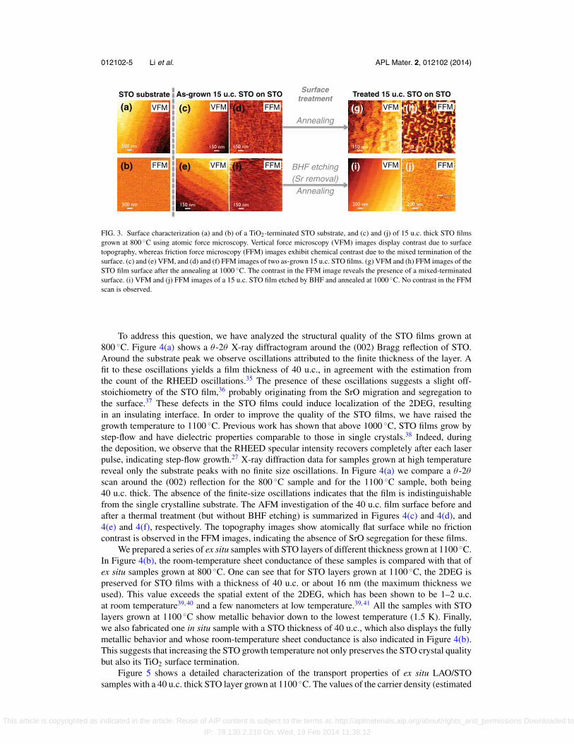
Figures 3(a) and 3(b) show the surface topography and the FFM images, respectively, of asingle-crystalline (001) STO substrate. Unit-cell-high step-and-terrace structure, a characteristicfeature of a miscut TiO2-terminated STO surface, can be clearly seen on the topographic image.Despite these unit-cell steps, no contrast is visible on the friction image, suggesting uniform TiO2
coverage. On top of such substrates, we grew 15 u.c. thick STO films, since for this layer thick-ness the in situ and ex situ LAO/STO/STO structures showed fundamentally different transportproperties (insulating and metallic, respectively). After the STO deposition, the surface becomesrougher, marked by the presence of nanometer-sized pits, islands, and rough step edges, as shown inFigures 3(c) and 3(e). This may already indicate that the TiO2 termination is no longer well main-tained and mixed termination appears. However, this feature is not resolved in the friction imagesshown in Figures 3(d) and 3(f), where no clear contrast is distinguishable. This may be due to the
This article is copyrighted as indicated in the article. Reuse of AIP content is subject to the terms at: http://aplmaterials.aip.org/about/rights_and_permissions Downloaded to
IP: 78.130.2.210 On: Wed, 19 Feb 2014 11:38:12

012102-4 Li et al. APL Mater. 2, 012102 (2014)
I+
I-
V1+V1-
V2+V2-
(a)
(b)
(c)
FIG. 2. Transport properties of the LAO/STO/STO samples with STO layers grown at 800 ◦C. (a) A sketch of theLAO/STO/STO sample with a Hall-bar pattern used to measure the sheet resistance and carrier density of the system.(b) Sheet conductance at 280 K; (c) −1/eRH at 5 K versus STO layer thickness d (u.c.). Black open (blue solid) circles arefor in situ (ex situ) samples. The shaded areas in (b) and (c) indicate the room-temperature sheet conductance and −1/eRH at5 K, respectively, in standard LAO/STO interfaces. The lines are guides to the eye.
fact that the termination of the surface is mixed on sub-nanometer scale that is below the resolutionof FFM.
In order to detect the presence of SrO, we performed an annealing treatment in an oxygenatmosphere at ambient pressure on one 15 u.c. thick STO film. Such an annealing promotes themigration of surface species to the step edges,32, 33 and is routinely used as a complementary stepafter the buffered HF (BHF) etching to obtain the atomically flat TiO2 termination with sharpunit-cell step edges. Since a long high-temperature anneal may also promote SrO segregation onthe STO surface,34 we keep our annealing time below 2 h. Figures 3(g) and 3(h) illustrate thetopographic and friction images after the annealing treatment. In the friction scan, we observe theappearance of a clear contrast, with nanometer-sized white areas present at the terrace edges thatwe relate to the accumulation of SrO. In order to exclude the possible segregation of SrO duringthe annealing step, we performed a control experiment by treating an identical 15 u.c. thick STOfilm first with BHF and then with the same annealing process. The topography and friction imagesillustrated in Figures 3(i) and 3(j) do not suggest any presence of SrO as we do not observe anycontrast in the FFM scan. Therefore, using these treatment conditions, once the segregated SrOis removed by the BHF etching, the TiO2 termination is preserved during the high-temperatureannealing.
We can then conclude that the SrO segregation occurs on the film surface during STO growthand may be responsible for the loss of the 2DEG at the interface for in situ samples. We shouldalso note that this loss of the 2DEG properly highlights the fact that oxygen vacancies, which canpossibly be formed during the growth,23 seem not to be the relevant origin of the metallicity in thisstudy. Looking at Figures 2(b) and 2(c), however, raises the question: why is this loss also observedfor ex situ samples, albeit at higher STO critical thickness?
This article is copyrighted as indicated in the article. Reuse of AIP content is subject to the terms at: http://aplmaterials.aip.org/about/rights_and_permissions Downloaded to
IP: 78.130.2.210 On: Wed, 19 Feb 2014 11:38:12
012102-5 Li et al. APL Mater. 2, 012102 (2014)
STO substrateSurface
treatment
Annealing
BHF etching(Sr removal)Annealing
500 nm
(a) VFM
500 nm
(b)
As-grown 15 u.c. STO on STOA
150 nm
(c)
150 nm
(e)
150 nm
(d)
150 nm
(f)
200 nm
(i)
200 nm
(j)
150 nm
(g)
150 nm
(h)
Treated 15 u.c. STO on STO
FFM
VFM
VFM
FFM VFM
FFM
VFM
VFM
FFM
FFM
FIG. 3. Surface characterization (a) and (b) of a TiO2-terminated STO substrate, and (c) and (j) of 15 u.c. thick STO filmsgrown at 800 ◦C using atomic force microscopy. Vertical force microscopy (VFM) images display contrast due to surfacetopography, whereas friction force microscopy (FFM) images exhibit chemical contrast due to the mixed termination of thesurface. (c) and (e) VFM, and (d) and (f) FFM images of two as-grown 15 u.c. STO films. (g) VFM and (h) FFM images of theSTO film surface after the annealing at 1000 ◦C. The contrast in the FFM image reveals the presence of a mixed-terminatedsurface. (i) VFM and (j) FFM images of a 15 u.c. STO film etched by BHF and annealed at 1000 ◦C. No contrast in the FFMscan is observed.
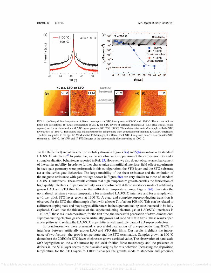
To address this question, we have analyzed the structural quality of the STO films grown at800 ◦C. Figure 4(a) shows a θ -2θ X-ray diffractogram around the (002) Bragg reflection of STO.Around the substrate peak we observe oscillations attributed to the finite thickness of the layer. Afit to these oscillations yields a film thickness of 40 u.c., in agreement with the estimation fromthe count of the RHEED oscillations.35 The presence of these oscillations suggests a slight off-stoichiometry of the STO film,36 probably originating from the SrO migration and segregation tothe surface.37 These defects in the STO films could induce localization of the 2DEG, resultingin an insulating interface. In order to improve the quality of the STO films, we have raised thegrowth temperature to 1100 ◦C. Previous work has shown that above 1000 ◦C, STO films grow bystep-flow and have dielectric properties comparable to those in single crystals.38 Indeed, duringthe deposition, we observe that the RHEED specular intensity recovers completely after each laserpulse, indicating step-flow growth.27 X-ray diffraction data for samples grown at high temperaturereveal only the substrate peaks with no finite size oscillations. In Figure 4(a) we compare a θ -2θ
scan around the (002) reflection for the 800 ◦C sample and for the 1100 ◦C sample, both being40 u.c. thick. The absence of the finite-size oscillations indicates that the film is indistinguishablefrom the single crystalline substrate. The AFM investigation of the 40 u.c. film surface before andafter a thermal treatment (but without BHF etching) is summarized in Figures 4(c) and 4(d), and4(e) and 4(f), respectively. The topography images show atomically flat surface while no frictioncontrast is observed in the FFM images, indicating the absence of SrO segregation for these films.
We prepared a series of ex situ samples with STO layers of different thickness grown at 1100 ◦C.In Figure 4(b), the room-temperature sheet conductance of these samples is compared with that ofex situ samples grown at 800 ◦C. One can see that for STO layers grown at 1100 ◦C, the 2DEG ispreserved for STO films with a thickness of 40 u.c. or about 16 nm (the maximum thickness weused). This value exceeds the spatial extent of the 2DEG, which has been shown to be 1–2 u.c.at room temperature39, 40 and a few nanometers at low temperature.39, 41 All the samples with STOlayers grown at 1100 ◦C show metallic behavior down to the lowest temperature (1.5 K). Finally,we also fabricated one in situ sample with a STO thickness of 40 u.c., which also displays the fullymetallic behavior and whose room-temperature sheet conductance is also indicated in Figure 4(b).This suggests that increasing the STO growth temperature not only preserves the STO crystal qualitybut also its TiO2 surface termination.
Figure 5 shows a detailed characterization of the transport properties of ex situ LAO/STOsamples with a 40 u.c. thick STO layer grown at 1100 ◦C. The values of the carrier density (estimated
This article is copyrighted as indicated in the article. Reuse of AIP content is subject to the terms at: http://aplmaterials.aip.org/about/rights_and_permissions Downloaded to
IP: 78.130.2.210 On: Wed, 19 Feb 2014 11:38:12
012102-6 Li et al. APL Mater. 2, 012102 (2014)
42 44 46 48 50
2
Inte
nsi
ty (
a.u.
)
40 u.c. STO1100 800
(a) (b)
AnnealingAnnealing
Surface treatment
40 u.c. STO on STO
150 nm
(c)
150 nm
(d)
200 nm
(e)
200 nm
(f)VFM FFM VFM FFM
FIG. 4. (a) X-ray diffraction patterns of 40 u.c. homoepitaxial STO films grown at 800 ◦C and 1100 ◦C. The arrows indicatefinite size oscillations. (b) Sheet conductance at 280 K for STO layers of different thickness d (u.c.). Blue circles (blacksquares) are for ex situ samples with STO layers grown at 800 ◦C (1100 ◦C). The red star is for an in situ sample with the STOlayer grown at 1100 ◦C. The shaded area indicates the room-temperature sheet conductance in standard LAO/STO interfaces.The lines are guides to the eye. (c) VFM and (d) FFM images of a 40 u.c. thick STO film grown on a TiO2-terminated STOsubstrate at 1100 ◦C. (e) VFM and (f) FFM images of the same sample after annealing at 1000 ◦C.
via the Hall effect) and of the electron mobility shown in Figures 5(a) and 5(b) are in line with standardLAO/STO interfaces.42 In particular, we do not observe a suppression of the carrier mobility and astrong localization behavior, as reported in Ref. 23. However, we also do not observe an enhancementof the carrier mobility. In order to further characterize this artificial interface, field-effect experimentsin back-gate geometry were performed; in this configuration, the STO layer and the STO substrateact as the series gate dielectrics. The large tunability of the sheet resistance and the evolution ofthe magneto-resistance with gate voltage shown in Figure 5(c) are very similar to those of standardLAO/STO interfaces. These results confirm that high temperature growth enables the fabrication ofhigh quality interfaces. Superconductivity was also observed at these interfaces made of artificiallygrown LAO and STO thin films in the millikelvin temperature range. Figure 5(d) illustrates thenormalized resistance versus temperature for a standard LAO/STO interface and for a sample witha 40 u.c. thick STO layer grown at 1100 ◦C. A clear and complete superconducting transition isobserved for the STO thin film sample albeit with a lower Tc of about 100 mK. This can be related toa different doping state and may suggest differences in the superconducting state that need to be fullyexplored. Given that the thickness of the superconducting electron gas at LAO/STO interfaces is∼10 nm,41 these results demonstrate, for the first time, the successful generation of a two-dimensionalsuperconducting electron gas between artificially grown LAO and STO thin films. These results opena new pathway to realize the LAO/STO superlattices with multiple parallel 2D superconductors.
In conclusion, we have presented a successful realization of a superconducting 2DEG atinterfaces between artificially grown LAO and STO thin films. Our results highlight the impor-tance of two factors—the growth temperature and the STO termination. Samples grown at 800 ◦Cdo not host the 2DEG for STO layer thicknesses above a critical value. The observation of nanoscaleSrO segregation on the STO surface by the local friction force microscopy and the presence ofdefects in the STO layer seems to be plausible origins for this behavior. Increasing the depositiontemperature for the STO layers to 1100 ◦C changes the growth mode to step-flow and produces
This article is copyrighted as indicated in the article. Reuse of AIP content is subject to the terms at: http://aplmaterials.aip.org/about/rights_and_permissions Downloaded to
IP: 78.130.2.210 On: Wed, 19 Feb 2014 11:38:12

012102-7 Li et al. APL Mater. 2, 012102 (2014)
(a)
(b)
(c)
(d)
FIG. 5. Magnetotransport properties and superconductivity of a LAO/STO/STO heterostructure with a STO layer of 40 u.c.grown at 1100 ◦C. (a) Inverse Hall constant and (b) the electron mobility as a function of temperature. (c) Magnetoresistanceat 1.5 K for different gate voltages Vg. (d) Normalized resistance R(T)/R(500 mK) as a function of temperature displayingsuperconducting transitions. Blue solid squares and black open circles are for a LAO/STO interface with artificially grownSTO layer and for a “standard” LAO/STO sample, respectively.
films of higher quality; a metallic, down to the lowest temperatures, and superconducting 2DEGis observed on these artificial LAO/STO interfaces even for thick STO layers. This study providesthe key ingredients needed to grow LAO/STO superlattices or interfaces on other substrates, whereexciting physical properties can be realized and studied.
We are deeply grateful for the fruitful discussions with Mathilde L. Reinle-Schmitt and toBenedikt Ziegler for the assistance with FFM measurements. We also thank Marco Lopes andSebastien Muller for the technical assistance. This work was supported by the Swiss NationalScience Foundation through the National Center of Competence in Research, Materials with NovelElectronic Properties, MaNEP and Division II.
1 P. Zubko, S. Gariglio, M. Gabay, P. Ghosez, and J.-M. Triscone, Annu. Rev. Condens. Matter Phys. 2, 141 (2011).2 H. Y. Hwang, Y. Iwasa, M. Kawasaki, B. Keimer, N. Nagaosa, and Y. Tokura, Nature Mater. 11, 103 (2012).3 A. Ohtomo and H. Y. Hwang, Nature (London) 427, 423 (2004).4 S. Thiel, G. Hammerl, A. Schmehl, C. W. Schneider, and J. Mannhart, Science 313, 1942 (2006).5 N. Nakagawa, H. Y. Hwang, and D. A. Muller, Nature Mater. 5, 204 (2006).6 C. Cancellieri, D. Fontaine, S. Gariglio, N. Reyren, A. D. Caviglia, A. Fete, S. J. Leake, S. A. Pauli, P. R. Willmott, M.
Stengel, P. Ghosez, and J.-M. Triscone, Phys. Rev. Lett. 107, 056102 (2011).7 M. L. Reinle-Schmitt, C. Cancellieri, D. Li, D. Fontaine, M. Medarde, E. Pomjakushina, C. W. Schneider, S. Gariglio,
P. Ghosez, J.-M. Triscone, and P. R. Willmott, Nat. Commun. 3, 932 (2012).8 Y. Xie, C. Bell, T. Yajima, Y. Hikita, and H. Y. Hwang, Nano Lett. 10, 2588 (2010).9 J. Mannhart and D. G. Schlom, Science 327, 1607 (2010).
10 R. Pentcheva and A. E. Pickett, J. Phys.: Condens. Matter 22, 043001 (2010).11 N. Reyren, S. Thiel, A. D. Caviglia, L. F. Kourkoutis, G. Hammerl, C. Richter, C. W. Schneider, T. Kopp, A.-S. Ruetschi,
D. Jaccard, M. Gabay, D. A. Muller, J.-M. Triscone, and J. Mannhart, Science 317, 1196 (2007).12 A. D. Caviglia, S. Gariglio, N. Reyren, D. Jaccard, T. Schneider, M. Gabay, S. Thiel, G. Hammerl, J. Mannhart, and J.-M.
Triscone, Nature (London) 456, 624 (2008).13 B. Forg, C. Richter, and J. Mannhart, Appl. Phys. Lett. 100, 053506 (2012).
This article is copyrighted as indicated in the article. Reuse of AIP content is subject to the terms at: http://aplmaterials.aip.org/about/rights_and_permissions Downloaded to
IP: 78.130.2.210 On: Wed, 19 Feb 2014 11:38:12
012102-8 Li et al. APL Mater. 2, 012102 (2014)
14 C. Cen, S. Thiel, J. Mannhart, and J. Levy, Science 323, 1026 (2009).15 D. Stornaiuolo, S. Gariglio, N. J. G. Couto, A. Fete, A. D. Caviglia, G. Seyfarth, D. Jaccard, A. F. Morpurgo, and J.-M.
Triscone, Appl. Phys. Lett. 101, 222601 (2012).16 S. Thiel, C. Schneider, L. Kourkoutis, D. Muller, N. Reyren, A. D. Caviglia, S. Gariglio, J.-M. Triscone, and J. Mannhart,
Phys. Rev. Lett. 102, 046809 (2009).17 B. Jalan, S. J. Allen, G. E. Beltz, P. Moetakef, and S. Stemmer, Appl. Phys. Lett. 98, 132102 (2011).18 M. R. Fitzsimmons, N. W. Hengartner, S. Singh, M. Zhernenkov, F. Y. Bruno, J. Santamaria, A. Brinkman, M. Huijben,
H. J. A. Molegraaf, J. de la Venta, and I. K. Schuller, Phys. Rev. Lett. 107, 217201 (2011).19 Z. Salman, O. Ofer, M. Radovic, H. Hao, M. Ben Shalom, K. H. Chow, Y. Dagan, M. D. Hossain, C. D. P. Levy, W. A.
MacFarlane, G. M. Morris, L. Patthey, M. R. Pearson, H. Saadaoui, T. Schmitt, D. Wang, and R. F. Kiefl, Phys. Rev. Lett.109, 257207 (2012).
20 J.-M. Triscone and Ø. Fischer, Rep. Prog. Phys. 60, 1673 (1997).21 C. W. Bark, D. A. Felker, Y. Wang, Y. Zhang, H. W. Jang, C. M. Folkman, J. W. Park, S. H. Baek, H. Zhou, D. D. Fong,
X. Q. Pan, E. Y. Tsymbal, M. S. Rzchowski, and C. B. Eom, Proc. Natl. Acad. Sci. U.S.A. 108, 4720 (2011).22 J. W. Park, D. F. Bogorin, C. Cen, D. A. Felker, Y. Zhang, C. T. Nelson, C. W. Bark, C. M. Folkman, X. Q. Pan, M. S.
Rzchowski, J. Levy, and C. B. Eom, Nat. Commun. 1, 94 (2010).23 T. Hernandez, C. W. Bark, D. A. Felker, C. B. Eom, and M. S. Rzchowski, Phys. Rev. B 85, 161407 (2012).24 P. Brinks, W. Siemons, J. E. Kleibeuker, G. Koster, G. Rijnders, and M. Huijben, Appl. Phys. Lett. 98, 242904 (2011).25 M. Kawasaki, K. Takahashi, T. Maeda, R. Tsuchiya, M. Shinohara, O. Ishiyama, T. Yonezawa, M. Yoshimoto, and H.
Koinuma, Science 266, 1540 (1994).26 J. Nishimura, A. Ohtomo, A. Ohkubo, Y. Murakami, and M. Kawasaki, Jpn. J. Appl. Phys. 43, L1032 (2004).27 See supplementary material at http://dx.doi.org/10.1063/1.4854335 for more experimental details, sample growth charac-
terizations, detailed transport properties, and friction force microscopic measurement test.28 M. L. Reinle-Schmitt, C. Cancellieri, S. J. Leake, E. Pomjakushina, P. R. Willmott, A. Cavallaro, and J. A. Kilner,
arXiv:1312.2486 (2013).29 M. Huijben, A. Brinkman, G. Koster, G. Rijnders, H. Hilgenkamp, and D. H. A. Blank, Adv. Mater. 21, 1665 (2009).30 J. Fompeyrine, R. Berger, H. P. Lang, J. Perret, E. Machler, C. Gerber, and J.-P. Locquet, Appl. Phys. Lett. 72, 1697 (1998).31 K. Iwahori, S. Watanabe, M. Kawai, K. Mizuno, K. Sasaki, and M. Yoshimoto, J. Appl Phys. 88, 7099 (2000).32 G. Koster, G. Rijnders, D. Blank, and H. Rogalla, Physica C 339, 215 (2000).33 T. Ohnishi, K. Shibuya, M. Lippmaa, D. Kobayashi, H. Kumigashira, M. Oshima, and H. Koinuma, Appl. Phys. Lett. 85,
272 (2004).34 R. Bachelet, F. Sanchez, F. J. Palomares, C. Ocal, and J. Fontcuberta, Appl. Phys. Lett. 95, 141915 (2009).35 For this measurement, we have used a film thicker than 15 u. c. in order to better observe the contribution of the layer.36 A. Ohtomo and H. Y. Hwang, J. Appl. Phys. 102, 083704 (2007).37 We note that this slight off-stoichiometry may also be induced by the laser fluency used in this study. The influence of the
laser fluency on the STO thin-films grown at this temperature requires further investigation.38 M. Lippmaa, N. Nakagawa, M. Kawasaki, S. Ohashi, Y. Inaguma, M. Itoh, and H. Koinuma, Appl. Phys. Lett. 74, 3543
(1999).39 O. Copie, V. Garcia, C. Bodefeld, C. Carretero, M. Bibes, G. Herranz, E. Jacquet, J.-L. Maurice, B. Vinter, S. Fusil, K.
Bouzehouane, H. Jaffres, and A. Barthelemy, Phys. Rev. Lett. 102, 216804 (2009).40 M. Sing, G. Berner, K. Goß, A. Muller, A. Ruff, A. Wetscherek, S. Thiel, J. Mannhart, S. Pauli, C. Schneider, P. Willmott,
M. Gorgoi, F. Schafers, and R. Claessen, Phys. Rev. Lett. 102, 176805 (2009).41 N. Reyren, S. Gariglio, A. D. Caviglia, D. Jaccard, T. Schneider, and J.-M. Triscone, Appl. Phys. Lett. 94, 112506 (2009).42 C. Cancellieri, N. Reyren, S. Gariglio, A. D. Caviglia, A. Fete, and J.-M. Triscone, Europhys. Lett. 91, 17004 (2010).
This article is copyrighted as indicated in the article. Reuse of AIP content is subject to the terms at: http://aplmaterials.aip.org/about/rights_and_permissions Downloaded to
IP: 78.130.2.210 On: Wed, 19 Feb 2014 11:38:12