
F 1 Advanced Transmission Electron Microscopy Techniques...
28
________________________ Lecture Notes of the 43rd IFF Spring School "Scattering Methods for Condensed Matter Research: Towards Novel Applications at Future Sources" (Forschungszentrum Jülich, 2012). All rights reserved. F 1 Advanced T ransmission Electron Microscopy Techniques and Applications R.E. Dunin-Borkowski, M. Feuerbacher, M. Heggen, L. Houben, A. Kovács, M. Luysberg, A. Thust and K. Tillmann Ernst Ruska-Centre for Microscopy and Spectroscopy with Electrons Forschungszentrum Jülich GmbH Contents 1 Introduction ................................................................................................... 2 2 Aberration correction in high-resolution TEM .......................................... 3 3 Aberration correction in high-resolution STEM ........................................ 9 4 Electron energy-loss spectroscopy.............................................................. 12 5 Electron tomography ................................................................................... 17 6 Electron holography of magnetic and electric fields ................................ 19 Acknowledgments ............................................................................................. 26 References .......................................................................................................... 26
Transcript of F 1 Advanced Transmission Electron Microscopy Techniques...

________________________ Lecture Notes of the 43rd IFF Spring School "Scattering Methods for Condensed Matter Research: Towards Novel Applications at Future Sources" (Forschungszentrum Jülich, 2012). All rights reserved.
F 1 Advanced Transmission Electron Microscopy Techniques and Applications
R.E. Dunin-Borkowski, M. Feuerbacher, M. Heggen, L. Houben,
A. Kovács, M. Luysberg, A. Thust and K. Tillmann
Ernst Ruska-Centre for Microscopy and Spectroscopy with Electrons
Forschungszentrum Jülich GmbH Contents
1 Introduction ................................................................................................... 2
2 Aberration correction in high-resolution TEM .......................................... 3
3 Aberration correction in high-resolution STEM ........................................ 9
4 Electron energy-loss spectroscopy .............................................................. 12
5 Electron tomography ................................................................................... 17
6 Electron holography of magnetic and electric fields ................................ 19
Acknowledgments ............................................................................................. 26
References .......................................................................................................... 26

F1.2 R.E. Dunin-Borkowski
1 Introduction Modern transmission electron microscopes (TEMs) can be used to obtain quantitative measurements of the structural, electronic and chemical properties of materials on length scales down to the sub-Å level [1-3]. In the last decade, electron microscopy has been revolutionized by the introduction of aberration correctors, monochromators and imaging filters, as well as by improvements in computing power for microscope control, image analysis and image simulation. Specialized techniques have also been developed, including the use of in situ gas reaction electron microscopy to study growth processes and chemical reactions in materials at elevated temperature and pressure and the application of bright and dark field electron holography to measure variations in electrostatic potential, magnetic induction and crystallographic strain in materials with sub-5-nm spatial resolution. A photograph of a modern aberration corrected transmission electron microscope is shown in Fig. 1.
Fig. 1: FEI Titan 80-300 field emission transmission electron microscope at
Forschungszentrum Jülich. The instrument is equipped with a spherical aberration corrector on the objective lens and has an information limit of 0.08 nm
The basic operation of a TEM is in many respects analogous to that of a light optical microscope. The electron source at the top of the column is either a thermionic emitter such as a LaB6 single crystal or a field emitter such as a zirconia-coated tungsten tip. The primary advantage of a field emission source is that it is brighter, as a result of the smaller extraction area for electrons, which can be only a few nm in size. After emission, the electrons are accelerated by a voltage of typically between 80 and 300 kV and focused onto the specimen

Advanced TEM F1.3
by 2-3 condenser lenses. The specimen is most commonly a 3 mm disk that is prepared to be extremely thin at its centre, as the typical specimen thickness for high-resolution imaging is below 10 nm. The specimen stage allows movement of the sample in three spatial directions and tilting about two axes. The objective lens is located directly below the specimen and has a short focal length of 1-2 mm. Its design and the stability of its power supply are crucial for the optical performance of the microscope. The intermediate and projector lenses in the lower part of the column are used for magnification of the image and have a relatively small influence on image quality. After passing the projector lens, the electrons can be observed on a fluorescent screen or recorded on a CCD (charge coupled device) camera. Active vibration damping systems and electromagnetic field compensation systems are normally required to create a sufficiently stable environment for a state of the art electron microscope.
2 Aberration correction in high-resolution TEM High-resolution transmission electron microscopy (HRTEM) involves the acquisition of images in a TEM with a spatial resolution that is sufficient to separate single atomic columns. The interpretation of such images is, however, not straightforward, as the recorded intensity is not a direct representation of the specimen but an interference pattern that is affected both by the strength of the interaction of the incident electrons with the specimen and by the contrast transfer of the microscope [4]. The interaction of an incoming electron wave with a TEM specimen can be calculated by solving the relativistically corrected Schrödinger equation for the electron wavefunction
!
"(r) in a periodic crystal potential
!
V (r) according to the Bethe-Bloch formalism [5]. However, in practice, several approximations are often used to understand the image formation process. In the phase object approximation (POA) for a thin specimen, atoms in the sample are simulated by a projected potential that is continuous and constant in the direction of the incident beam. The electron wavefunction at specimen thickness t is then written in the form
!(r,!t) " exp[i! (r ,!t)]= exp[i! VP (r )t] , (1)
where ϕ is the phase of the electron wave, σ is an interaction constant and VP is the projected crystal potential. The weak phase object approximation (WPOA) assumes that the phase modulation of the electron wave is small in a very thin specimen, resulting in the expression
!(r, t) "1+ i!(r, t) =1+ i! Vp(r)t (2)
The effect of the microscope lenses is described by modifying the exit plane wavefunction using a phase factor
!
exp ["i# ] in the form
! i (g) =!(g)exp["i! (g)] (3)

F1.4 R.E. Dunin-Borkowski
where, for the rotationally symmetric aberrations of a round lens, the aberration function
! (g) = 2" 14CS #
3 g4 + 12Z # g2
!
"#
$
%& . (4)
In Eq. 4,
!
" is the wavelength of the electron beam,
!
Z is the defocus and
!
CS is the coefficient of spherical aberration of the objective lens, which cannot be avoided for a round electromagnetic lens [6] and describes the deviation of rays passing the outer part of a lens compared to near-axis rays and the resultant blurring of the object, as shown in Fig. 2.
Fig. 2: Schematic illustration of (a) positive spherical aberration, (b) no spherical
aberration and (c) negative spherical aberration. For a thin specimen, the WPOA results in an expression for the linear image intensity of the form
!
IL(g " 0) # 2$V (g) t sin % (g) , (5)
from which it is apparent that the optimum image contrast is obtained when the coherent contrast transfer function (CTF)
!
sin " = ±1, i.e., when
!
" (g) is an odd multiple of
!
" / 2 for all values of
!
g. However, sin ! is in general a function that oscillates strongly with
!
g . As a result, atomic columns that are arranged periodically with a spacing of
!
d = 1/ g are imaged as white dots only at selected spatial frequencies for which the CTF is close to 1. At spatial frequencies for which the CTF is close to –1, the atomic columns are imaged as black dots, while they may be invisible if the spatial frequency corresponding to their interatomic spacing coincides with a zero of the CTF. In order to approach ideal phase contrast transfer behaviour, a defocus setting can be chosen that balances the g2 and g4 terms in the aberration function,

Advanced TEM F1.5
allowing for a relatively broad band of frequencies to be transferred with a CTF close to −1. This defocus setting
!
ZS " #43
CS $ . (6)
is known as Scherzer defocus [7]. The point resolution
!
dS = 1/ gS is defined by the first zero crossing of the CTF at the Scherzer defocus and is given by the expression
!
gS "3
16CS #
3$
% &
'
( )
*14 .
(7)
Typical values of the point resolution of commercially available medium voltage microscopes with accelerating voltages of 200-400 kV are in the range 0.24 to 0.17 nm. The limited coherence of the electron source and electronic instabilities have the additional effect of multiplying the coherent CTF by envelope functions, which result in a cut-off of the contrast transfer at high spatial frequencies. The spatial frequency at which the partially coherent CTF falls below a threshold value defines the information limit of the microscope. For an uncorrected field emission TEM, the information limit can be higher than the point resolution, leading to strong oscillations in the partially coherent CTF and blurring effects in images. Figure 3 shows sin ! for a 200 kV instrument for two different values of CS. At higher spatial frequencies the CTF oscillates rapidly up to the information limit. If CS is reduced then a broad transfer band extends up to the information limit of 0.125 nm, improving the point resolution significantly.
Fig. 3: Partially coherent contrast transfer functions at Scherzer defocus conditions
calculated for a CM20 FEG microscope operated at 200 kV for (left) CS = 1.2 mm, and (right) CS = 0.04 mm.
An important approach that can be used to overcome the effect of the strongly oscillating part of the CTF between the point resolution and the information limit for an uncorrected microscope is to use numerical reconstruction of the exit plane wavefunction from a defocus

F1.6 R.E. Dunin-Borkowski
series of 10–20 images acquired from the same object area [8-11], as shown schematically in Fig. 5. According to the phase object approximation, the heights of the phase maxima in the wavefunction are approximately proportional to the projected crystal potential for a thin specimen, permitting the chemical distinction of atomic species. The availability of the complex-valued wavefunction also enables complete correction of all aberrations in software. The resulting wavefunction is then free from artefacts introduced by the microscope, making it possible to resolve light elements such as C, N and O close to or even below 0.1 nm spatial resolution.
Fig. 4: Principle of focal series restoration. A series of images is recorded from the same
object area using different settings of the objective lens defocus. The quantum-mechanical exit plane wavefunction, which consists of amplitude and phase, can be retrieved from the series by means of numerical procedures.
The elimination of delocalisation by focal series restoration using non-linear reconstruction from 20 images is shown in Fig. 5 for a twin boundary in BaTiO3. The left side of Fig. 5 shows one image from the focal series, which was taken with an uncorrected Philips CM20ST FEG microscope. Blurring of the image due to objective lens aberrations is visible. The right side of Fig. 5 shows the phase of the restored wavefunction, in which blurring is no longer present and all atomic positions are resolved up to the information limit of the microscope.
Fig. 5: Example of focal series restoration. (a) Representative image from a series of 20
images of twinned [110] oriented BaTiO3. (b) Phase of restored exit plane wavefunction. All aberrations have been removed numerically. Positions of atomic columns are revealed by phase maxima.

Advanced TEM F1.7
The elimination of spherical aberration using hardware is now also possible using multipole lenses. The first successful demonstration of spherical aberration correction was achieved in the late 1990s in a project funded by the Volkswagenstiftung involving Forschungszentrum Jülich [12, 13]. By tuning the spherical aberration coefficient and other higher order aberrations, optimum contrast transfer and a dramatic improvement in resolution can be achieved. Figure 6 shows a comparison between an experimental defocus series of [110] SrTiO3 recorded using a
!
CS corrected Philips CM200ST FEG microscope and simulated images. The structure image predicted by simulations for a defocus of +10 nm appears in the experiment.
Fig. 6: Comparison of an experimental defocus series of SrTiO3 oriented along [110] with
simulated images. The experimental images were acquired with a CS corrected CM200ST FEG microscope using a value for CS of –0.04 mm. Simulated images are shown on the left, with experimental images on the right. The defocus values of the simulated images are indicated. The specimen thickness used in the simulations was 3.5 nm. Half of a SrTiO3 cell projected along [110] is indicated by the white frame.
The ability to tune the spherical aberration coefficient opens up new ways to record directly interpretable images. In particular, the choice of a small negative value for CS results in strong contrast from light atomic columns, which appear bright [14]. In this negative CS imaging (NCSI) technique, paraxial rays travelling through the objective lens come to focus ahead of the outer rays and light elements such as oxygen in Pb(Zr0.2Ti0.8)O3 adjacent to columns of heavy atoms can be resolved [15]. It should be noted that the complete aberration function is made up of many individual aberrations. Sub-Å imaging requires both a knowledge of all significant wave aberrations up to sixth order in g and the stability of these aberrations over the length of an experiment [16]. The decomposition of a typical aberration function into its components is illustrated in Fig. 7, while the time stability of the defocus measured for two microscopes is show in Fig. 8.

F1.8 R.E. Dunin-Borkowski
Fig. 7: Aberration function (centre) and its decomposition into basic aberrations. Positive
values of the aberration function are depicted in red and negative values in blue. Sawtooth jumps occur at intervals of π/4. The yellow circle marks a value of g = 12.5 nm−1 , corresponding to a resolution of 0.08 nm. Aberration-free imaging is achieved when the modulus of the total aberration function does not exceed π/4 within the circle defining the resolution limit.
Fig. 8: Time variation of the objective lens defocus during a period of approximately 2
minutes for (a) a 200 kV Philips CM200 microscope with a resolution of 0.12 nm and (b) a 300 kV FEI Titan microscope with a resolution of 0.08 nm. Both a thermally induced long-term drift and short-term fluctuations caused by instabilities of the accelerating voltage and the objective lens current are observed.

Advanced TEM F1.9
A graphical illustration of the dramatic improvement in image resolution and interpretability with microscope generation and the use of spherical aberration correction is shown in Fig. 9 for simulated images of AlN.
Fig. 9: Simulation of an AlN crystal viewed along the [113] zone axis using different
transmission electron microscopes operated at optimised conditions (Scherzer defocus and Lentzen focus).
3 Aberration correction in high-resolution STEM Figure 10 shows a schematic illustration of a scanning TEM (STEM), in which a focused electron beam is scanned across the specimen. For each position of the probe, an on-axis bright field detector or a high-angle annular dark field (HAADF) detector collects electrons that interacted with the specimen. The same microscope can be used for HRTEM and STEM if a microscope such as that shown in Fig. 1 is equipped with a scanning unit located above the specimen and detectors in the diffraction plane. In order to achieve a resolution in the sub-Å range, a STEM has to be equipped with an aberration corrector for the condenser lens.
Fig. 10: In STEM the probe is scanned across the specimen. For each position of the probe,
electrons are collected by a bright field or annular dark field detector. A spectrometer can also be used to record an electron energy-loss spectrum.

F1.10 R.E. Dunin-Borkowski
The resolution in STEM is determined primarily by the size of the probe. The probe function is in turn determined by parameters that include the diameter of the condenser aperture and the aberrations of the condenser lens system. Correction of the aberrations of the condenser lenses is crucial to obtain sub-Å resolution in HAADF imaging. Under certain assumptions, the image intensity in annular dark field images is given by the convolution of the square of the probe function and the square of the specimen transmission function. The image formation process can be regarded as incoherent if the inner angle of the annular detector is much larger than the diameter of the condenser aperture, which defines the convergence angle of the illumination. Typically, only electrons that have been scattered to sufficiently large angles on the order of 100 mrad (compared to about 20 mrad for the semi-angle of the condenser aperture) must be collected by the detector. For a sufficiently thin specimen, the image intensity is to a first approximation proportional to the atomic number Z raised to the power 1.7. However, the image can also be affected by beam broadening as the electron probe travels through the specimen and by dynamical diffraction. A recent application of STEM to the characterization of a complex metallic alloys (CMA) is illustrated in Fig. 11. Such materials have unusual electronic transport [17], magnetic [18] and plastic [19] properties and novel types of dislocations, which are referred to as metadislocations [20]. In the T-Al-Mn-Pd phase, which is orthorhombic with lattice parameters a = 1.47 nm, b = 1.25 nm, and c = 1.26 nm, a deformation mechanism based on the movement of a novel type of dislocation was found. Figure 12 shows an aberration-corrected HAADF STEM image of a dislocation taken along the b direction of the T-phase structure [21, 22]. The unit cell (left blue rectangle) contains 156 atoms. The unit cell can be divided into structural subunits represented by elongated hexagonal tiles (white and yellow polygons) arranged in rows of alternating orientation, mutually tilted by 36°. White dots in the centres of the hexagons correspond to columns containing Pd, while the columns at the edges and vertices of the hexagons contain mainly Mn. The core of the dislocation is represented by a green polygon, which has a complex (1 0 0) mirror symmetric shape and a Burgers vector b = c ! 4 0 0 1( ) with b = 0.184 nm, where ( )1521 +=τ is the golden mean.
The Burgers vector is a small fraction of the c lattice constant of the T-phase. The dislocation trails a planar defect, which, upon closer inspection at high-magnification, appears to be a nm-thick slab of the so-called R-phase. This R-phase slab is visible at the right side of the dislocation core. On the left side of the dislocation, three bowtie-shaped tiles, shown in red, are required to complete the area-filling tiling. The bowtie-shaped tiles are line defects along the b direction but are not dislocations, since they have no Burgers vectors. During plastic deformation, the bow-tie shaped tiles move ahead of the dislocation core to rearrange the structure, i.e., to clear the way for the dislocation. The dislocation creates a slab of R-phase in its wake and creates a shear-induced transformation from the T- to the R-phase in a slab of about 5 nm thickness. For a single elementary glide step of the dislocation, a coordinated movement of a few hundred atoms is required.

Advanced TEM F1.11
Fig. 11: High-resolution HAADF-STEM micrograph of a dislocation in CMA T-Al-Mn-Pd.
White and yellow hexagons represent structural subunits of the T-phase (left) and R-phase (right). The unit cells are shown by blue rectangles. The dislocation core is represented by a green polygon. The dislocation is escorted by three bowtie-shaped tiles (red).
A second illustration of the application of aberration-corrected HRTEM and STEM is shown in Fig. 12. The images were obtained from semiconductors that contain transition metal atoms introduced with the intention of combining ferromagnetic and semiconducting properties for the design of spin-electronic devices [23]. In such materials, ferromagnetism can result from the presence of nanoscale clusters of magnetic atoms or randomly located diluted transition metal impurities or defects. In these studies, care was devoted to cross-sectional TEM specimen preparation to minimize artefacts. Figure 12(a) shows an aberration-corrected HRTEM image of a Mn-doped GaAs layer grown by molecular beam epitaxy containing hexagonal (NiAs-type) MnAs crystals, adjacent voids and As nanocrystals. Figure 13(b) shows an aberration-corrected HAADF STEM image of an Fe-doped GaN layer grown by metalorganic chemical vapour deposition containing Fe-rich nitride nanocrystals associated with N2 filled bubbles.
Fig. 12: (a) Aberration-corrected HRTEM image of hexagonal MnAs, orthorhombic As and a
void in a GaAs host. (b) Aberration-corrected HAADF STEM image of an Fe3N nanocrystal and an adjacent N2 bubble in a GaN host. The ADF inner semi-angle used was 47.4 mrad.
F1.12 R.E. Dunin-Borkowski
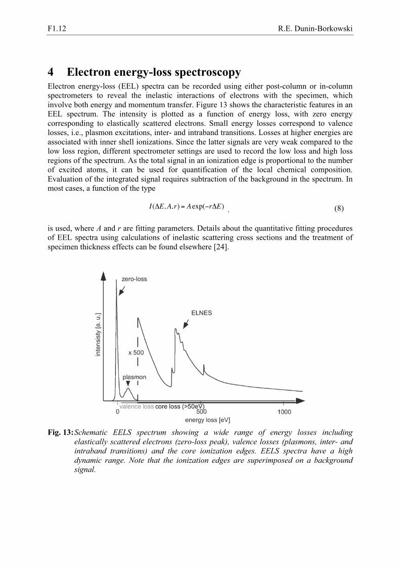
4 Electron energy-loss spectroscopy Electron energy-loss (EEL) spectra can be recorded using either post-column or in-column spectrometers to reveal the inelastic interactions of electrons with the specimen, which involve both energy and momentum transfer. Figure 13 shows the characteristic features in an EEL spectrum. The intensity is plotted as a function of energy loss, with zero energy corresponding to elastically scattered electrons. Small energy losses correspond to valence losses, i.e., plasmon excitations, inter- and intraband transitions. Losses at higher energies are associated with inner shell ionizations. Since the latter signals are very weak compared to the low loss region, different spectrometer settings are used to record the low loss and high loss regions of the spectrum. As the total signal in an ionization edge is proportional to the number of excited atoms, it can be used for quantification of the local chemical composition. Evaluation of the integrated signal requires subtraction of the background in the spectrum. In most cases, a function of the type
I(!E,A, r) = Aexp("r!E) . (8) is used, where A and r are fitting parameters. Details about the quantitative fitting procedures of EEL spectra using calculations of inelastic scattering cross sections and the treatment of specimen thickness effects can be found elsewhere [24].
Fig. 13: Schematic EELS spectrum showing a wide range of energy losses including
elastically scattered electrons (zero-loss peak), valence losses (plasmons, inter- and intraband transitions) and the core ionization edges. EELS spectra have a high dynamic range. Note that the ionization edges are superimposed on a background signal.

Advanced TEM F1.13
The energy loss near edge structure (ELNES) shown in Fig. 13 contains information about the local chemical environment of an excited atom. Two models, displayed Fig. 14, are used to understand edge structure: (a) a band structure model, in which an electron from a shell is excited into unoccupied states above the Fermi level; (b) a multiple scattering model describing ELNES by an outgoing wave, which is scattered by the surrounding atoms. The intensity of the edge scales primarily with the density of final states.
Fig. 14: Schematic representation of two models for the origin of electron energy-loss near-
edge structures (ELNES) for core-ionization edges. (a) Transition of strongly bound core electrons into unoccupied states (b) multiple scattering description of ELNES.
Figure 15 shows representative background-subtracted EEL spectra recorded from an Fe-doped GaN semiconductor. In this material, depending on the growth temperature used, Fe can either be distributed homogenously in the GaN host lattice or it can accumulate in the form of Fe-N nanocrystals. In the present specimen, Fe-N nanocrystal formation was observed in samples that had been deposited at temperatures higher than 850°C. Most of the Fe-N nanocrystals were found to be associated with closely adjacent void-like features. EELS was used to show that these features are bubbles filled with molecular N2. In order to interpret the experimental results, N K edge spectra were calculated for GaN using self-consistent real-space multiple-scattering calculations with FEFF 9.05. Figure 15 shows an EELS measurement recorded from a single nanocrystal embedded in the GaN host. A 100 kV accelerating voltage and a distributed-dose acquisition routine [25] were used to minimize and control electron beam induced damage during the experiment. Figure 15(a) shows N K edge spectra recorded from the nanocrystal, the adjacent N2-containing region and the GaN host. The N K edge shows a three-peaked structure between 400 and 407 eV. Figure 15 (b) shows an experimental spectrum acquired from the bubble alongside an experimental spectrum from N2 taken from the EELS Atlas [26] and a simulation of a GaN spectrum.

F1.14 R.E. Dunin-Borkowski
Fig. 15: (a) Background-subtracted N K edge spectra measured from an Fe-N nanocrystal, a
N2 bubble and the GaN host lattice in Fe-doped GaN. (b) Experimental spectra acquired from a nitrogen bubble alongside an experimental measurement from N2 taken from the EELS Atlas and simulated spectra calculated for GaN.
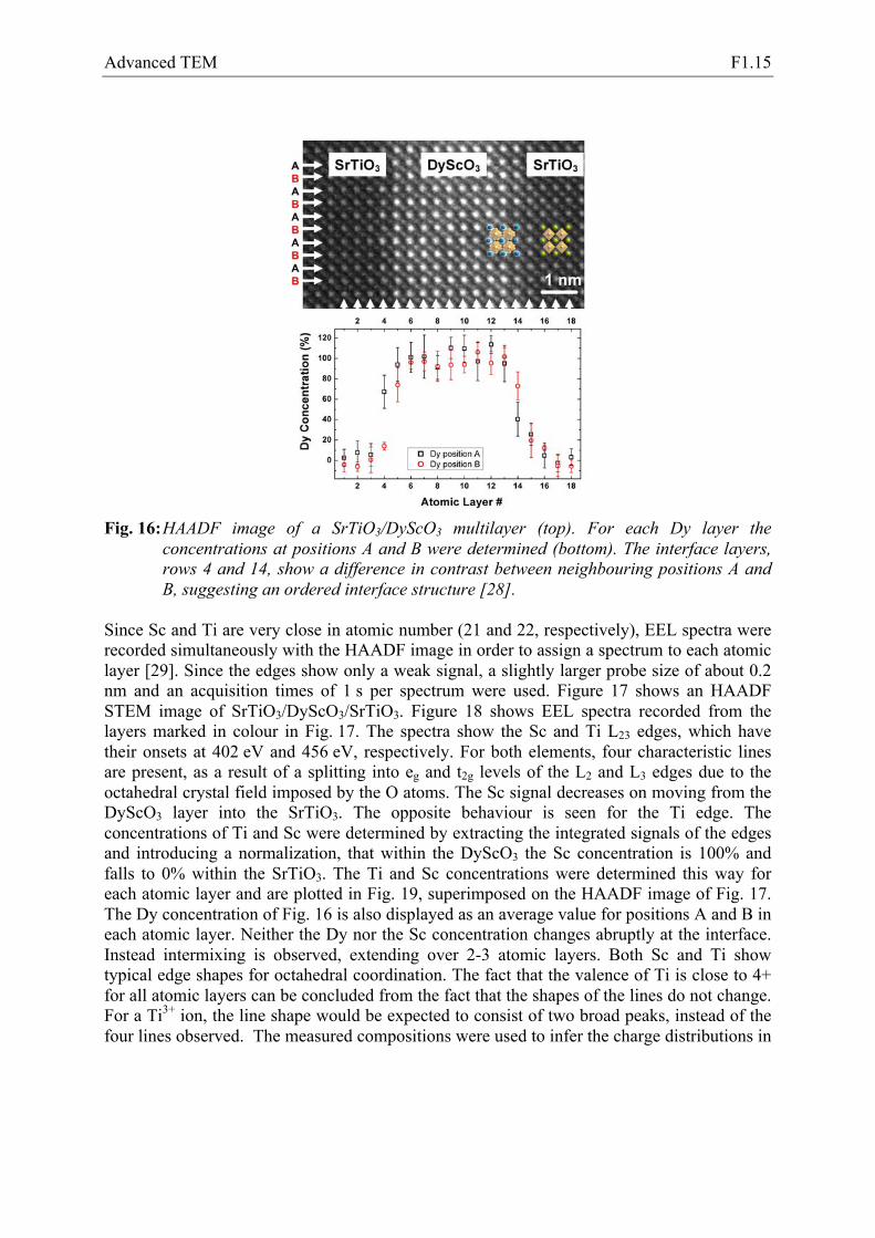
The simultaneous application of high-resolution STEM and EELS can be used to access chemical information about a specimen on the atomic scale. A focused electron beam is scanned across the sample. For each (x,y) position both the HAADF signal and the EEL signal are recorded. Figures 16-18 illustrate the application of HAADF STEM and EELS to measure the compositions across DyScO3/SrTiO3 interfaces. The atomic structure of the DyScO3 layer in SrTiO3 is revealed in the aberration corrected HAADF STEM image shown in Fig. 16, which was recorded using a probe size of 0.08 nm. The intensity of each atom column reflects differences in atomic number. Here DyScO3 is imaged along the [101] direction of the orthorhombic unit cell, resulting in a zigzag arrangement of the Dy columns parallel to the interface [27]. Sc and Ti atoms are located at the centre of the oxygen octahedra (displayed in orange in the structure models) and produce weaker contrast compared to Sr and Dy. The oxygen atoms cannot be resolved. Along the interfaces, in rows 4 and 14, the contrast at the Dy/Sr positions alternates between neighbouring columns. This is seen in the image as well as in the concentration profile. The concentrations were determined by quantification of the intensities using Gaussian fits to the contrast at each atom position in Fig. 16. In each row the intensities of five equivalent positions (A and B) were averaged. Error bars denote the standard deviation obtained from concentration values in regions of constant composition. The Dy concentration was obtained by calculating the integrated intensity to the power of 0.5 and normalizing to 100% within the DyScO3 layer and 0% within the SrTiO3 layer. In row 4 of Fig. 16, the positions labelled “A” are brighter than positions B. The opposite behaviour is seen in row 14, where positions B show the highest intensity, suggesting the presence of an ordered interface structure.
Advanced TEM F1.15
Fig. 16: HAADF image of a SrTiO3/DyScO3 multilayer (top). For each Dy layer the
concentrations at positions A and B were determined (bottom). The interface layers, rows 4 and 14, show a difference in contrast between neighbouring positions A and B, suggesting an ordered interface structure [28].
Since Sc and Ti are very close in atomic number (21 and 22, respectively), EEL spectra were recorded simultaneously with the HAADF image in order to assign a spectrum to each atomic layer [29]. Since the edges show only a weak signal, a slightly larger probe size of about 0.2 nm and an acquisition times of 1 s per spectrum were used. Figure 17 shows an HAADF STEM image of SrTiO3/DyScO3/SrTiO3. Figure 18 shows EEL spectra recorded from the layers marked in colour in Fig. 17. The spectra show the Sc and Ti L23 edges, which have their onsets at 402 eV and 456 eV, respectively. For both elements, four characteristic lines are present, as a result of a splitting into eg and t2g levels of the L2 and L3 edges due to the octahedral crystal field imposed by the O atoms. The Sc signal decreases on moving from the DyScO3 layer into the SrTiO3. The opposite behaviour is seen for the Ti edge. The concentrations of Ti and Sc were determined by extracting the integrated signals of the edges and introducing a normalization, that within the DyScO3 the Sc concentration is 100% and falls to 0% within the SrTiO3. The Ti and Sc concentrations were determined this way for each atomic layer and are plotted in Fig. 19, superimposed on the HAADF image of Fig. 17. The Dy concentration of Fig. 16 is also displayed as an average value for positions A and B in each atomic layer. Neither the Dy nor the Sc concentration changes abruptly at the interface. Instead intermixing is observed, extending over 2-3 atomic layers. Both Sc and Ti show typical edge shapes for octahedral coordination. The fact that the valence of Ti is close to 4+ for all atomic layers can be concluded from the fact that the shapes of the lines do not change. For a Ti3+ ion, the line shape would be expected to consist of two broad peaks, instead of the four lines observed. The measured compositions were used to infer the charge distributions in

F1.16 R.E. Dunin-Borkowski
the layers, and the fact that a predicted ”polar catastrophe” is overcome by an adjustment to the chemical compositions of the individual atomic layers.
Fig. 17: Z contrast image of the Dy ScO3/SrTiO3
multilayer system recorded within 100 s the arrows mark the layers, which correspond to the EEL spectra in Fig 17
Fig. 18: EEL spectra of layers 12.5 through 15.5, revealing the Sc L23 edge at 402 eV and the Ti L23 edges at 456 eV.
Fig. 19: HAADF image of SrTiO3/DyScO3. The fast scan direction runs from bottom to top.
Superimposed are the average Dy concentrations as red triangles (average of positi-ons A and B in Fig. 16) as well as Sc (yellow circles) and Ti (yellow open squares) concentrations for each atom row. Error bars denote the standard deviation obtained from concentration values in regions of constant composition.

Advanced TEM F1.17
5 Electron tomography A significant development in electron tomography for the measurement of the three-dimensional morphology, density or composition of an object is illustrated in Figs 20 and 21. The advance involves the development of an improved alignment procedure for a tilt series of recorded images. Previously, algorithms for three-dimensional reconstruction, such as backprojection or algebraic reconstruction, assumed a precise knowledge of the projection geometry and the absence of any image displacements prior to reconstruction. The most widely used techniques for image alignment in electron tomography were developed for the biological sciences and are based on pattern matching by correlation techniques [30, 31] or by the tracking of fiducial markers [32, 33]. These methods are useful at low and medium magnification, with automated schemes for alignment facilitating the refinement process [34, 35]. However, cross-correlation and marker based methods have disadvantages. Successive cross-correlation of images in a tilt series can only produce an approximate alignment since three-dimensional rotation around a common axis is not taken into account and the image changes with viewing direction. Alignment errors can accumulate during the procedure [36, 37], resulting in a loss of high-resolution detail in the tomogram. Tracking of marker points in sinogram space does account for the three-dimensional rotation but it relies on the presence of object details which can serve as a markers or landmarks. Methods that use the reconstruction feedback of the tomogram iteratively to improve image alignment have been proposed and demonstrated in the literature. These methods include manual feedback control, iterative optimizations in the form of alignment to pseudo-projections of a tomogram sequence [38], three-dimensional model based approaches that align with respect to expected projections of automatically or pre-identified specimen features and area matching as an extension of the cosine stretching used in cross-correlation alignment [39]. A recently developed variant of feedback optimization is the iterative refinement of the tomogram contrast and resolution [40], which does not depend on user assisted motif recognition or the presence of extrinsic markers. Flow charts of the conventional and new algorithm are shown in Fig. 20. The optimization loop of the refinement algorithm provides a correct model of the three-dimensional motion of the object and maximizes the tomogram resolution. Simulation data demonstrate that translational displacement accuracy better than the width of the point spread function in an individual image can be achieved. Experimental tomographic reconstructions at medium resolution show that the marker-free alignment procedure is competitive with fiducial marker alignment and removes artefacts after consecutive cross-correlation alignment [40]. Figure 21 demonstrates the application of the procedure to the reconstruction of WS2 nanotubes. In this example, no obvious nodal points can be identified and self-markers cannot be utilized. A further complication is that the bundle of nanotubes shows significant motif change in projection during tilt. In such an example, image alignment based on cross correlation is likely to fail. After refinement, the sinogram traces of the tube shells follow the expected projection and no shape distortion is seen in the tomogram slices, apart from residual missing wedge artefacts.

F1.18 R.E. Dunin-Borkowski
Fig. 20: Flowchart for refinement of image alignment for tomographic reconstruction from
tilt series of images. (a) Conventional procedure involving alignment of images prior to reconstruction. (b) New algorithm including iterative loop.
Fig. 21: Comparison of conventional and new alignment for reconstruction of a bundle of
WS2 nanotubes. (a) and (b) are images from the tilt series. The lines mark the outer shells of two nanotubes. (c) shows a sinogram (left) after conventional cross-correlation alignment. The magnified lower part of the sinogram reveals a lack of correlation. (d) Tomogram slice showing the bundle in cross-section. (e) and (f) Sinogram and a tomogram slice after refinement of the alignment.

Advanced TEM F1.19
6 Electron holography of magnetic and electric fields Off-axis electron holography is a specialized TEM technique that can be used to characterize magnetic fields and electrostatic potentials in materials with sub-10-nm spatial resolution [41]. It is the only technique that provides direct access to the phase of the electron wave that has passed through a thin specimen, in contrast to TEM techniques that record only spatial distributions of image intensity (described above). The technique can be divided into two primary modes: (i) high-resolution electron holography, in which the interpretable resolution in lattice images is improved by the use of software phase plates to correct for electron microscope lens aberrations [42] and (ii) medium-resolution electron holography, in which magnetic fields and electrostatic potentials within and around materials are studied with nanometre spatial resolution [43]. Some of the most successful early examples of the application of medium-resolution electron holography were the experimental confirmation of magnetic flux quantization in superconducting toroids and the study of magnetic flux vortices in superconductors [44]. Here, more recent developments and applications of medium-resolution electron holography for the study of nanoscale materials are described. A schematic diagram showing the typical electron-optical configuration for off-axis electron holography is shown in Fig. 22a. The region of interest is positioned so that it covers approximately half the field of view. A biprism (a thin conducting wire), which is usually located close to the first image plane, has a positive voltage applied to it to overlap a "reference" electron wave that passed through vacuum with the electron wave that passed through the specimen. The overlap region contains interference fringes and an image of the specimen, in addition to Fresnel fringes from the edge of the biprism wire (Figs 22b-e). The electron-optical configuration is equivalent to the use of two electron sources S1 and S2.
Fig. 22: (a) Schematic diagram of the setup for off-axis electron holography. (b-e)
Interference fringe patterns (electron holograms) recorded from vacuum using biprism voltages of (b) 0 V, (c) 60 V and (d,e) 120 V. In (b), only Fresnel fringes from the edges of the biprism are visible. (e) corresponds to the box marked in (d). The field of view in (b)-(d) is 916 nm.

F1.20 R.E. Dunin-Borkowski
The intensity in an off-axis electron hologram consists of the reference image intensity, the specimen image intensity and a set of cosinusoidal fringes. A representative hologram of a specimen that contains a chain of magnetite (Fe3O4) crystals is shown in Fig. 23a, alongside a vacuum hologram (Fig. 23b) and a magnified region of the specimen hologram (Fig. 23c). In order to extract phase and amplitude information from an electron hologram, it is Fourier transformed. The Fourier transform contains a peak at the origin corresponding to the Fourier transform of the reference image, a peak at the origin corresponding to the Fourier transform of a bright field image of the specimen, a peak at q = -qc corresponding to the Fourier transform of the image wavefunction and a peak at q = +qc corresponding to the Fourier transform of the complex conjugate of the wavefunction. Figure 23d shows the Fourier transform of the hologram shown in Fig. 23a. In order to recover the complex wavefunction, one of the “sidebands” in the Fourier transform is selected (Fig. 23e) and inverse Fourier transformed. The amplitude and phase are then calculated. The phase image is initially calculated modulo 2π, meaning that 2π discontinuities appear where the phase exceeds this amount (Fig. 23g). The phase image can be “unwrapped” by using suitable algorithms, as shown in Fig. 23h. In Fig. 23d, the streak from the "centerband" toward the sidebands is attributed to the presence of Fresnel fringes from the biprism wire, which can lead to artefacts in the reconstructed amplitude and phase. This effect can be minimized by masking the streak from the Fourier transform before inverse Fourier transformation (Fig. 23e).
Fig. 23: Processing steps required to convert a recorded electron hologram into an amplitude
and phase image. (a) Hologram of a chain of magnetite crystals. The overlap width and holographic interference fringe spacing are 650 and 3.3 nm, respectively. The field of view is 725 nm. (b) Vacuum hologram acquired after the specimen hologram. (c) Magnified region of the specimen hologram. (d) Fourier transform of (a). (e) One of the sidebands extracted from the Fourier transform, shown after applying a circular mask with smooth edges. The streak from the Fresnel fringes can be removed by assigning a value of zero to pixels inside the region shown by the dashed line. Inverse Fourier transformation of the sideband is used to provide a complex image wave, which is displayed in the form of (f) an amplitude image and (g) a modulo 2π phase image. Phase unwrapping algorithms are used to remove the 2π phase discontinuities from (g) to yield an unwrapped phase image shown in (h).
Advanced TEM F1.21
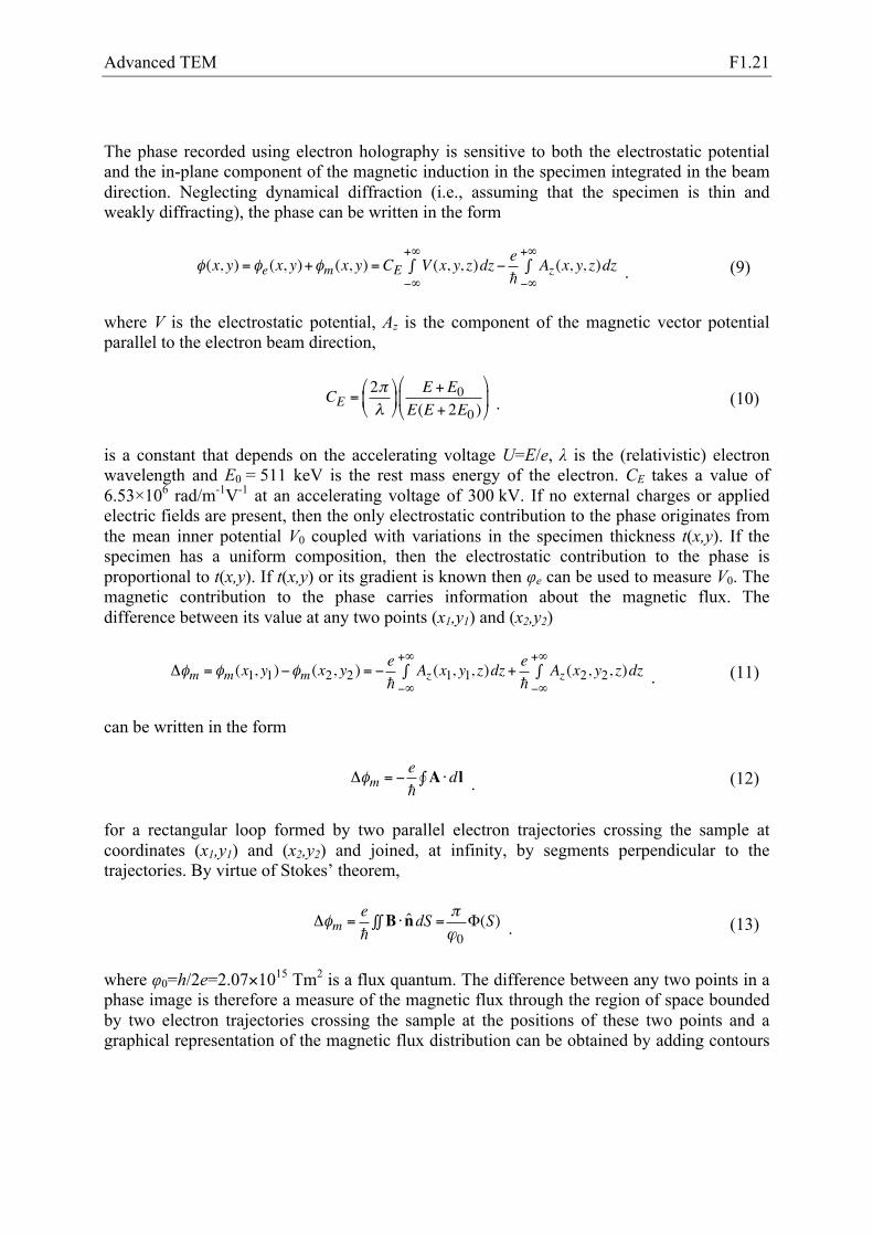
The phase recorded using electron holography is sensitive to both the electrostatic potential and the in-plane component of the magnetic induction in the specimen integrated in the beam direction. Neglecting dynamical diffraction (i.e., assuming that the specimen is thin and weakly diffracting), the phase can be written in the form
!(x, y) = !e(x, y)+!m (x, y) =CE V (x, y, z)dz!"
+"# !
e!
Az (x, y, z)dz!"
+"# . (9)
where V is the electrostatic potential, Az is the component of the magnetic vector potential parallel to the electron beam direction,
CE =2!"
!
"#
$
%&
E +E0E(E + 2E0 )!
"#
$
%& . (10)
is a constant that depends on the accelerating voltage U=E/e, λ is the (relativistic) electron wavelength and E0 = 511 keV is the rest mass energy of the electron. CE takes a value of 6.53×10⁶ rad/m-1V-1 at an accelerating voltage of 300 kV. If no external charges or applied electric fields are present, then the only electrostatic contribution to the phase originates from the mean inner potential V0 coupled with variations in the specimen thickness t(x,y). If the specimen has a uniform composition, then the electrostatic contribution to the phase is proportional to t(x,y). If t(x,y) or its gradient is known then φe can be used to measure V0. The magnetic contribution to the phase carries information about the magnetic flux. The difference between its value at any two points (x1,y1) and (x2,y2)
!!m = !m (x1, y1)"!m (x2, y2 ) = "e!
Az (x1, y1, z)dz"#
+#$ +
e!
Az (x2, y2, z)dz"#
+#$ . (11)
can be written in the form
!!m = "e!A #d l!$ . (12)
for a rectangular loop formed by two parallel electron trajectories crossing the sample at coordinates (x1,y1) and (x2,y2) and joined, at infinity, by segments perpendicular to the trajectories. By virtue of Stokes’ theorem,
!!m =e!
B " n̂dS =##"#0
$(S) . (13)
where φ0=h/2e=2.07×1015 Tm2 is a flux quantum. The difference between any two points in a phase image is therefore a measure of the magnetic flux through the region of space bounded by two electron trajectories crossing the sample at the positions of these two points and a graphical representation of the magnetic flux distribution can be obtained by adding contours

F1.22 R.E. Dunin-Borkowski
to a phase image. A phase difference of 2π corresponds to an enclosed magnetic flux of 4.14×10¹⁵ Tm2. The relationship between the magnetic contribution to the phase and the magnetic induction can be established from the gradient of φm . In the special case when stray fields can be neglected, the sample has a constant thickness and the magnetic induction does not vary with z in the specimen, the magnetic contribution to the phase gradient is proportional to the magnetic induction. When characterizing magnetic materials, the microscope objective lens is usually turned off because it creates a large (>2 T) magnetic field at the position of the specimen. Instead, a non-immersion Lorentz lens can be used as the imaging lens. This lens allows specimens to be imaged at relatively high magnification in magnetic-field-free conditions. The spherical aberration coefficient of this lens is large (e.g., 8400 mm for an FEI Titan), resulting in a point resolution of ~2 nm. It should be noted that the separation of electrostatic and magnetic contributions to the phase is almost always mandatory in order to obtain quantitative magnetic information from a phase image. The few instances when this step may be avoided include the special case of magnetic domains in a film of constant thickness (far from the specimen edge). The contribution of the mean inner potential to the phase can be much greater than the magnetic contribution for small (sub-50-nm) magnetic nanocrystals. Separation of the magnetic contribution from the recorded phase is then essential. In principle, the most accurate way of achieving this separation involves turning the specimen over after acquiring a hologram and acquiring a second hologram from the same region. The sum and difference of the holograms are then used to determine twice the mean inner potential and twice the magnetic contribution to the phase, respectively. An alternative method, which is often more practical, involves performing a magnetization reversal experiment in the microscope and then selecting pairs of holograms that differ only in the magnetization direction in the specimen. If the magnetization in the specimen does not reverse perfectly, then such reversal measurements may need to be repeated many times so that non-systematic differences between reversed images are averaged out. Figure 24 shows magnetic contributions to the phase and magnetic induction maps measured from three self-assembled rings of 25-nm-diameter polycrystalline Co nanoparticles using off-axis electron holography [45]. Each particle comprises a core of hexagonal-close-packed Co and a shell of ~3 nm of CoO. Holograms were recorded in zero-field conditions after applying chosen out-of-plane magnetic fields in situ in the TEM by partially exciting the conventional microscope objective lens. The mean inner potential contribution to the phase was calculated from phase images that had been acquired before and after turning the specimen over. Their sum and difference were used to determine twice the mean inner potential and twice the magnetic contribution to the phase, respectively. Once the mean inner potential contribution had been determined, it was subtracted from all subsequent phase images acquired from the same region of the specimen. The resulting phase images were smoothed slightly and phase contours and colours were used to form the final induction maps. An out-of-plane field of -20,000 Oe was initially applied perpendicular to the plane of the specimen and reduced to zero. The sample was then taken out of the TEM in zero field, turned over and put back into

Advanced TEM F1.23
the microscope. Chosen out-of-plane fields were then applied to the specimen in the TEM in succession by changing the current in the TEM objective lens. The applied field was reduced to zero before recording each hologram. Magnetization reversal of most rings could be achieved by using out-of-plane fields of between 1600 and 2500 Oe.
Fig. 24: Top row: Bright-field TEM images of rings of polycrystalline Co nanoparticles.
Subsequent rows: Magnetic contributions to the phase and magnetic induction maps recorded with the specimen in magnetic-field-free conditions using off-axis electron holography after saturating the rings using a large (-20,000 Oe) out-of-plane magnetic field and then applying the indicated out-of-plane fields in succession. The direction of the projected magnetic induction is shown using both contours and colours. (Red=right; blue=up; green=left; yellow=down). The magnetic phase contour spacing is 0.065 rad, corresponding to 96 × phase amplification.

F1.24 R.E. Dunin-Borkowski
Figure 25 shows the application of electron holography to study the current-induced motion of transverse and vortex-type magnetic domain walls in permalloy (NiFe) zigzag lines on Si3N4 windows [46]. Figure 25(b) shows the sequential positions of a magnetic domain wall that was subjected to 10 µs pulses with a current density of 3.14×10¹¹ A/m2. Electron holograms were acquired at each of these positions. A transverse magnetic domain wall initially formed at a kinked region of the wire after the application of a magnetic field. After applying a current pulse, the wall moved by 2330 nm in the direction of electron flow and transformed into a vortex-type wall. After a second pulse, the vortex-type wall moved in the same direction and became distorted, with the long axis of the vortex increasingly perpendicular to the wire length. This behaviour may be associated with edge roughness or defects, which may restrict movement of the wall. After a third pulse, the domain wall moved 260 nm further and retained its vortex state.
Fig. 25: (a) Low magnification bright-field image of permalloy (NiFe) zigzag wires (width: 430 nm, thickness: 11 nm) patterned on a Si3N4 window using lithography. A kink in one wire was examined using electron holography in the TEM. (b) Higher magnification bright-field image of a permalloy wire and magnetic induction maps measured using off-axis electron holography, showing the positions of a magnetic domain wall after the injection of 10 µs current pulses with a current density of 3.14×10¹¹ A/m2. The arrow in the top image indicates the direction of electron flow. The phase contour spacing in the magnetic induction maps is 0.785 radians.
One of the most important applications of medium-resolution off-axis electron holography is the measurement of electrostatic potentials in semiconductor devices, in order to fulfil the requirements of the semiconductor industry for a quantitative dopant profiling technique that has nm-scale spatial resolution. Such measurements are often made from site-specific regions

Advanced TEM F1.25
of semiconductor devices by using focused ion beam milling with Ga ions to prepare the TEM specimen. Unfortunately, focused ion beam milling can affect the electrical properties of the specimen as a result of the creation of defects that can extend to a depth of more than 100 nm. Approaches such as low energy ion milling can then be used to reduce the thicknesses of the damaged regions, although they do not remove them entirely. The effects of specimen preparation and illumination by the high energy electron beam on the measured electrical properties are presently being addressed by several research groups [48]. Figure 25 illustrates the recent application of electron holography to the measurement of the electrostatic potential within and around a carbon nanotube that has a voltage applied to it in situ in the TEM [49]. Figures 26 (a) and (b) show defocused bright-field images of the specimen, while Fig. 26(c) shows a phase image of one nanotube acquired using off-axis electron holography. The charge distribution along the nanotube was determined by analysing the gradient of the recorded phase image. In this way, the nanotube in Fig. 26(c) was inferred to have two different charge densities along its length (2.3 and 4.5 e/nm).
Fig. 26: (a) Underfocus and (b) overfocus images (defocus ~3 mm) of carbon nanotubes protruding from a nanotube bundle with an applied bias of 50 V created by a Au electrode (not shown) 5 µm away. (c) Phase image acquired from the region indicated in (b) with 1.5 rad phase contours superimposed.
Figure 27 illustrates the application of the recently developed technique of dark-field electron holography to measure the strain distribution in an InAs quantum dot grown in InP using low pressure metal organic vapour-phase epitaxy at 520 °C. The maximum strain measured in the centre of the dot, relative to the unstrained substrate, is 5.4±0.1%. Comparisons of the strain measurements with computer simulations suggest that the As concentration in the wetting layer is 29% InAs and the composition of the centre of the dot is 100% InAs [50]. Recent developments in medium resolution off-axis electron holography include the development of new approaches for the acquisition, analysis and simulation of electron holograms, the design and use of specimen holders that allow electrical contacts to be applied to magnetic devices in situ in the electron microscope, and the comparison of recorded magnetic induction maps both with micromagnetic simulations and with three-dimensional

F1.26 R.E. Dunin-Borkowski
information about the local compositions and morphologies of the same specimens acquired using electron tomography. In the future, the development electron holography will require new approaches for the careful separation of weak magnetic signals from unwanted contributions to recorded phase images. Further work is also required to increase the sensitivity of the technique for measuring weak fields and to improve its time resolution. The prospect of characterizing magnetic vector fields inside nanocrystals in three dimensions by combining electron tomography with electron holography is also of great interest.
Fig. 27: (a) Dark-field off-axis electron hologram of an InAs quantum dot in InP, with the 004 diffraction spot selected. (b) Strain map for the 004 growth direction derived from (a). (c) Strain profile extracted from the region indicated by the dashed line in (b) (solid line) compared to simulation (dashed line).
Acknowledgments We are grateful to J. Barthel, M. Bar Sadan, G. Pozzi, A. Wei, P. A. Midgley, D. Cooper, M.R. McCartney. C.B. Boothroyd. B. Schaffer, M. S. Moreno, T. Kasama, M. Beleggia, A.J. Craven, M. Kläui, J.L. Rouvière, A. Béché, S. Kadkhodazadeh, E.S. Semenova, K. Yvind, M. Eltschka, M. Wötzel, L.J. Heyderman, S. Hoffmann, A. Bonanni, T. Dietl and other colleagues for discussions and ongoing collaborations.
References [1] J.C.H. Spence, High-Resolution Electron Microscopy (Oxford University Press, New
York, 2003) [2] L. Reimer and H. Kohl, Transmission Electron Microscopy: Physics of Image
Formation (Springer, New York, 2008) [3] D.B. Williams and C.B. Carter, Transmission Electron Microscopy: A Textbook for
Materials Science (Plenum Press, New York, 2009)

Advanced TEM F1.27
[4] A. Thust, in: Vorlesungsmanuskripte des 29. Ferienkurses des Instituts für Festkörperforschung, Schriften des Forschungszentrums Jülich, Reihe Materie und Material, Band 1, 1998
[5] H. Bethe, Ann. Phys. 87, 55 (1928) [6] O. Scherzer, Z. Phys. 101, 593 (1936) [7] O. Scherzer, J. Appl. Phys. 20, 20 (1949) [8] P. Schiske, Proc. 4th Eur. Conf. on Electron Microscopy, Rome, 145 (1968) [9] W.M.J. Coene, A. Thust, M. Op de Beeck and D. van Dyck, Ultramicroscopy 64, 109
(1996) [10] A. Thust, W.M.J. Coene, M. Op de Beeck and D. van Dyck, Ultramicroscopy 64, 211
(1996) [11] C. Kisielowski, C.J.D. Hetherington, Y.C. Wang, R. Kilaas, M.A. O’Keefe, A. Thust,
Ultramicroscopy 89, 243 (2001) [12] M. Haider, H. Rose, S. Uhlemann, E. Schwan, B. Kabius and K. Urban,
Ultramicroscopy 75, 53 (1998) [13] M. Lentzen, B. Jahnen, C.L. Jia, A. Thust, K. Tillmann and K. Urban, Ultramicroscopy
92, 233 (2002) [14] C. L. Jia, M. Lentzen, and K. Urban, Science 299, 870 (2003) [15] C.L. Jia, S.B. Mi, K. Urban, I. Vrejoiu, M. Alexe and D. Hesse, Nature Materials 7, 57
(2008) [16] J. Barthel and A. Thust, Ultramicroscopy 111, 27 (2010) [17] M. Andersson, M. Feuerbacher and Ö. Rapp, Phys. Rev. B 78, 024201 (2008) [18] J. Dolinšek, J. Slanovec, Z. Jagličić, M. Heggen, S. Balanetskyy, M. Feuerbacher and
K. Urban, Phys. Rev. B 77, 064430 (2008) [19] S. Roitsch, M. Heggen, M. Lipinska-Chwalek and M. Feuerbacher, Intermetallics 15,
833 (2007) [20] M. Feuerbacher and M. Heggen, Phil. Mag. 86, 935 (2006) [21] M. Heggen, L. Houben and M. Feuerbacher, Nature Materials 9, 332 (2010) [22] M. Heggen, L. Houben and M. Feuerbacher, Acta Mater. 59, 4458 (2011) [23] T. Dietl, Nature Materials. 9, 965 (2011) [24] R.F. Egerton, Electron Energy-Loss Spectroscopy in the Electron Microscope (Springer,
New York, 2011) [25] K. Sader, B. Schaffer, G. Vaughan, R. Brydson, A. Brown and A. Bleloch,
Ultramicroscopy 110, 998 (2010) [26] C.C. Ahn and O.L. Krivanek, EELS Atlas (Gatan, 1983) [27] M. Boese, T. Heeg, J. Schubert and M. Luysberg, Journal of Materials Science 41, 4434
(2006) [28] M. Luysberg, M. Heidelmann, L. Houben, M. Boese, T. Heeg, J. Schubert and
M. Roeckerath, Acta Materialia 57, 3192 (2009) [29] M. Heidelmann, J. Barthel and L. Houben, Ultramicroscopy 109, 1447 (2009) [30] R. Guckenberger, Ultramicroscopy 9, 167 (1982) [31] J. Frank and B.F. McEwan, in: J. Frank (Ed.), Electron Tomography: Three-
Dimensional Imaging with the Transmission Electron Microscope (Plenum Press, New York, 1992)

F1.28 R.E. Dunin-Borkowski
[32] M.C. Lawrence, in: J. Frank (Ed.), Electron Tomography: Three-Dimensional Imaging with the Transmission Electron Microscope (Plenum Press, New York, 1992)
[33] D.N. Mastronarde, in: J. Frank (Ed.), Electron Tomography: Methods for Three-Dimensional Visualization of Structures in the Cell (Springer: New York, 2006)
[34] J.C. Fung, W. Liu, W.J. De Ruijter, H. Chen, C.K. Abbey, J.W. Sedat and D.A. Agard, Journal of Structural Biology 116, 181 (1996)
[35] S. Brandt and U. Ziese, Journal of Microscopy 222, 1(2006) [36] W.O. Saxton, W. Baumeister and M. Hahn, Ultramicroscopy 13, 57 (1984) [37] J. Frank, B.F. McEwen and M. Radermacher, Journal of Electron Microscopy
Technique 6, 193 (1987) [38] C.H. Owen and W.J. Landis, Ultramicroscopy 63, 27 (1996) [39] H. Winkler and K.A. Taylor, Ultramicroscopy 106, 240 (2006) [40] L. Houben and M. Bar Sadan, Ultramicroscopy 111, 1512 (2011) [41] D. Gabor, D, Proc. Roy. Soc. A, 197, 454 1949) [42] M. Lehmann, H. Lichte, D. Geiger, G. Lang and E. Schweda, Mater. Character., 42, 249
(1999) [43] R.E. Dunin-Borkowski, M.R. McCartney and D.J. Smith, in H.S. Nalwa (Ed.),
Encyclopedia of Nanoscience and Nanotechnology, Vol. 3, pp.41-100 (American Scientific Publishers, Stevenson Ranch, 2004).
[44] T. Matsuda, S. Hasegawa, M. Igarashi, T. Kobayashi, M. Naito, H. Kajiyama, J. Endo, N. Osakabe, A. Tonomura and R. Aoki, Phys. Rev. Lett. 62, 2519 (1989)
[45] T. Kasama, R.E. Dunin-Borkowski, M.R. Scheinfein, S.L. Tripp, J. Liu and A. Wei, Adv. Mater. 20, 4248 (2008)
[46] F. Junginger, M. Kläui, D. Backes, U. Rüdiger, T. Kasama, R.E. Dunin-Borkowski, L.J. Heyderman, C.A.F. Vaz and J.A.C. Bland, Appl. Phys. Lett. 88, 212510 (2007)
[47] M. Eltschka, M. Wötzel, J. Rhensius, S. Krzyk, U. Nowak, M. Kläui, T. Kasama, R.E. Dunin-Borkowski, L.J. Heyderman, H.J. van Driel, and R.A. Duine, Phys. Rev. Lett. 105, 056601 (2010)
[48] D. Cooper, R. Truche, P. Rivallin, J.M. Hartmann, F. Laugier, F. Bertin, A. Chabli and J.L. Rouviere, Appl. Phys. Lett. 91, 143501 (2007)
[49] M. Beleggia, T. Kasama, R.E. Dunin-Borkowski, S. Hofmann and G. Pozzi, Appl. Phys. Lett. 98, 243101 (2011)
[50] D. Cooper, J.L. Rouvière, A. Béché, S. Kadkhodazadeh, E.S. Semenova, K. Yvind and R.E. Dunin-Borkowski, Appl. Phys. Lett. 99, 261911 (2011)