Extraordinary Magnetoresistance in Encapsulated Graphene ...
134
Washington University in St. Louis Washington University Open Scholarship Arts & Sciences Electronic eses and Dissertations Arts & Sciences Spring 5-15-2019 Extraordinary Magnetoresistance in Encapsulated Graphene Devices Bowen Zhou Washington University in St. Louis Follow this and additional works at: hps://openscholarship.wustl.edu/art_sci_etds Part of the Condensed Maer Physics Commons is Dissertation is brought to you for free and open access by the Arts & Sciences at Washington University Open Scholarship. It has been accepted for inclusion in Arts & Sciences Electronic eses and Dissertations by an authorized administrator of Washington University Open Scholarship. For more information, please contact [email protected]. Recommended Citation Zhou, Bowen, "Extraordinary Magnetoresistance in Encapsulated Graphene Devices" (2019). Arts & Sciences Electronic eses and Dissertations. 1801. hps://openscholarship.wustl.edu/art_sci_etds/1801
Transcript of Extraordinary Magnetoresistance in Encapsulated Graphene ...

Washington University in St. LouisWashington University Open Scholarship
Arts & Sciences Electronic Theses and Dissertations Arts & Sciences
Spring 5-15-2019
Extraordinary Magnetoresistance in EncapsulatedGraphene DevicesBowen ZhouWashington University in St. Louis
Follow this and additional works at: https://openscholarship.wustl.edu/art_sci_etds
Part of the Condensed Matter Physics Commons
This Dissertation is brought to you for free and open access by the Arts & Sciences at Washington University Open Scholarship. It has been acceptedfor inclusion in Arts & Sciences Electronic Theses and Dissertations by an authorized administrator of Washington University Open Scholarship. Formore information, please contact [email protected].
Recommended CitationZhou, Bowen, "Extraordinary Magnetoresistance in Encapsulated Graphene Devices" (2019). Arts & Sciences Electronic Theses andDissertations. 1801.https://openscholarship.wustl.edu/art_sci_etds/1801

WASHINGTON UNIVERSITY IN ST. LOUIS
Department of Physics
Dissertation Examination Committee:
Erik Henriksen, Chair
Ken Kelton
Kater Murch
Chuan Wang
Li Yang
Extraordinary Magnetoresistance in Encapsulated Graphene Devices
by
Bowen Zhou
A dissertation presented to
The Graduate School
of Washington University in
partial fulfillment of the
requirements for the degree
of Doctor of Philosophy
May 2019
St. Louis, Missouri

© 2019, Bowen Zhou

ii
Table of Contents
List of Figures ....................................................................................................................................................... iv
List of Tables .......................................................................................................................................................... x
Acknowledgments ................................................................................................................................................ xi
Abstract of the Dissertation ............................................................................................................................... xv
Chapter 1: Introduction of Graphene ............................................................................................................ 1
1.1 Brief History of Graphene .................................................................................................................. 1
1.2 Lattice structure of Graphene............................................................................................................. 2
1.3 Band structure of Graphene ................................................................................................................ 4
1.4 Basic Physical Properties of Graphene ........................................................................................... 7
1.4.1 Charge Density and Fermi Level ............................................................................................. 7
1.4.2 Resistance ....................................................................................................................................... 9
1.4.3 Carrier Mobility .......................................................................................................................... 10
1.4.4 Mean Free Path, Diffusive and Ballistic Transport .......................................................... 12
Bibliography ..................................................................................................................................................... 13
Chapter 2: Fundamentals of Extraordinary Magnetoresistance ..................................................... 14
2.1 Theory of Extraordinary Magnetoresistance .............................................................................. 14
2.1.1 Lorentz Force .............................................................................................................................. 15
2.1.2 Mathematical illustrations ....................................................................................................... 17
2.2 First Discovery of Extraordinary Magnetoresistance .............................................................. 21
2.3 Extraordinary Magnetoresistance in 2D ...................................................................................... 26
2.4 More Simulations on Extraordinary Magnetoresistance ......................................................... 29
Bibliography .................................................................................................................................................... 33
Chapter 3: Extraordinary Magnetoresistance in Encapsulated Graphene Device .................... 35
Bibliography ..................................................................................................................................................... 42
Chapter 4: P-N Junction: Theory, Experiment and Simulation ......................................................... 44
4.1 Basics of P-N Junction ...................................................................................................................... 44
4.2 Metal-graphene Junction .................................................................................................................. 45
iii
4.2.1 Surface Contact between Graphene and Metal ................................................................. 46
4.2.2 𝜎 Bonds in Edge Contact and π Bonds in Surface Contact ........................................... 51
4.3 Experimental Discovery of Asymmetry in Gate-Voltage-Dependent Resistance of
Edge-Contact Graphene ................................................................................................................................. 53
4.4 Two Models ......................................................................................................................................... 55
4.5 Simulations in COMSOL ................................................................................................................. 66
Bibliography .................................................................................................................................................... 72
Chapter 5: Conclusion ..................................................................................................................................... 73
5.1 Summary ............................................................................................................................................... 73
5.2 Outlook .................................................................................................................................................. 74
Appendix A Instruments and Techniques .................................................................................................... 80
A.1 Probe Station and Stacking of Graphene ..................................................................................... 82
A.2 Scanning Electron Microscope and Electron beam Lithography .............................................. 83
A.3 Heidelberg Laser Writer .................................................................................................................... 87
A.4 Electron Beam Evaporator ................................................................................................................ 91
A.5 Thermal Evaporator ............................................................................................................................ 94
A.6 Reactive Ion Etching ........................................................................................................................... 96
A.7 Physical Property Measurement System ....................................................................................... 98
Bibliography .................................................................................................................................................... 99
Appendix B Measurement Circuit ............................................................................................................. 100
Appendix C Contact Resistance ................................................................................................................. 103
Appendix D Simulation by COMSOL Multiphysics ............................................................................. 109
iv
List of Figures
Figure 1.1 Example of scotch-tape exfoliated graphene. ………………………………………….2
Figure 1.2 Schematic of honeycomb lattice structure of graphene ……………………………… 3
Figure 1.3 Schematic of 𝜎 bond and 𝜋 bond in graphene. ………………………………………4
Figure 1.4 Schematic band structures of conductor, insulator, semiconductor and graphene……5
Figure 1.5 Electronic dispersion in the honeycomb lattice of graphene. Two inequivalent corners
of the Brillouin zone at the K and K’ valleys are known as the Dirac points………………………6
Figure 1.6 Schematic of a graphene flake sitting on an oxidized silicon substrate (left) and the
Fermi level in the band structure (right). ………………………………………………………….8
Figure 1.7 (Top) A plot of the resistance of a bilayer graphene device versus gate voltage; (bottom)
the corresponding schematic illustration of Fermi energy level in the band structure of graphene.
The Dirac point corresponds to the largest resistance of graphene. The Fermi level represented by
the grey line is set in the valence band corresponding to the negative gate voltage range suggesting
the graphene has charge carriers of holes. Likewise, it is in the positive gate voltage range if the
Fermi level is in the conduction band. ……………………………………………………………9
Figure 1.8 Schematic of four-wire measurement on graphene. ………………………………….10
Figure 2.1 Schematic of EMR device. …………………………………………………………..15
Figure 2.2 Simulation of electrical current in EMR device with zero field (left) and with high
magnetic field (right) by COMSOL Multiphysics. Colors represent the electric potential, red
means high and blue means low. Red arrows represent the current density, the larger the arrows
the higher density. Black contours represent the equipotential lines. ……………………………16
Figure 2.3 Schematic of EMR device made by Solin, et al. …………………………….………..21
Figure 2.4 Plot of MR versus the field of EMR device made by Solin, et al. The solid circle
represents the largest MR corresponding to the filling factor α =12/16. And the open square
represents the smallest MR corresponding to the filling factor α = 0. …………………………..22
Figure 2.5 Conformal mapping of EMR device. Cut a circular EMR device with four equal-spaced
contacts and unroll the metal and semiconductor and get the rectangular structure of two strips
formed by semiconductor and metal. The resulting four contacts are equal spaced………..…….24
v
Figure 2.6 Schematic of the device and simulation of electric potential and sensitivity. The two
current contacts are at the two ends of the device and the voltage contacts are in the middle……..24
Figure 2.7 Schematic of graphene based EMR device………………………………………..…26
Figure 2.8 MR of the chemical vapor deposition grown graphene device. The colors represent
different gate voltages (in V). The inset is the sensitivity with respect to the gate voltage………..28
Figure 2.9 Schematic (a) and scanning electron microscope image with fake color (b) of the
exfoliated graphene based EMR device. The contact configurations of the EMR measurements of
Solin’s device, the chemical vapor deposition grown graphene device and the exfoliated graphene
device are the same. …………………………………………………………...…………………28
Figure 2.10 Calculated MR vs the magnetic field in different mobility. With twice of mobility
increasement, the MR increases by around a half. ………………………………………………..28
Figure 2.11 Simulated MR vs the magnetic field in different conductivity ratios (left) and
mobilities (right). ………………………………………………………………………………...30
Figure 2.12 Simulated MR vs the magnetic field in different contact resistivities……………….31
Figure 2.13 Simulated MR vs the magnetic field in a multibranched geometry and a circular
geometry (left) and current distribution in the two geometries at zero field and 5 T (right). The
background color in the right figures represents the electric potential: brown means high, and blue
means low. ………………………………………………………………………………………32
Figure 2.14 A schematic for a 10 𝜇𝑚 square EMR device with contacts centered (left) and its MR
vs magnetic field for the central metal square of different sizes (right). The dashed lines represent
the MR for negative values of the magnetic field. ………………………………………………33
Figure 3.1 Schematic of honeycomb lattice structure of boron nitride. ………………………….36
Figure 3.2 (a) Microscope image of a set of three devices fabricated from a single graphene/hBN
stack. Contacts and central metallic shunt are made by edge contacts to exposed graphene.
Schematic shows side view of device geometry. (b) Magnetoresistance, 𝑀𝑅 = [𝑅(𝐵) − 𝑅0]/𝑅0],
for the device with highest observed EMR effect at room temperature. The MR shows a strong
dependence on back gate voltage. (c) The as-measured (un-normalized) resistance for the same
gate voltages as in (b). The resistance itself shows little change with 𝑉𝑔. (d) The sensitivity, dR/dB,
for the same device, at 𝑉𝑔 = − 4.2𝑉. The red (cyan) trace was calculated from data measured in a
four- (two-) terminal configuration. Note the log-scale of the B-field axis. ……………………37
Figure 3.3 The MR (a) and sensitivity (c) for devices with varying shunt-to-outer diameter ratios
but fixed outer diameter of 5.5 µm. The MR (b) and sensitivity (d) for devices with varying outer
diameter at fixed ratio 𝑟𝑎/𝑟𝑏 = 0.74 . Here all MR traces are measured in a four-terminal

vi
configuration, while the sensitivity is calculated from data acquired in a two-terminal voltage-
biased measurement. ……………………………………………………………………….……40
Figure 4.1 Schematic of a p-n junction and its electric potential. ………………………………45
Figure 4.2 Schematic side view of surface contact and edge contact between graphene and metal.
……………………………………………………………………………………………………46
Figure 4.3 Schematics of a graphene partly in contact with a metal showing the potential shift
caused by the charge transfer [1]. The upper plot shows two separate graphene: the graphene on
the metal surface is n-doped in this case, and the graphene far away from the metal is still free
standing and unperturbed. The lower plot shows when the two graphene connects, the
rearrangement of the charges give rise to the potential shift and band bending. …………………47
Figure 4.4 Measured room-temperature resistance (left) and calculated contact resistance (right)
of a graphene partly covered by metal as a function of gate voltage. Both plots have asymmetries
in which n branches are higher than the p branch in the traces, suggesting p-type doping in
graphene. And the asymmetries increase with the length (left) of the graphene channel and
characteristic width (right). The inset in the left plot is scanning electron image of the graphene
device covered by 7 metal contacts made from palladium and gold. And the inset in the right plot
is schematic of the potential of graphene vs the distance, the left and right parts of the profile
represent the potentials of graphene under the metal and in channel respectively.………………48
Figure 4.5 Calculated energy differences as a function of gate voltage. The red, green and blue
traces are for the graphene under the metal, and the grey trace is for the graphene channel without
the metal coverage. ………………………………………………………………………………49
Figure 4.6 Calculated contact resistance as a function of gate bias using different potential profiles
with the fixed 𝑊𝐵=40 nm. The inset are different potential profiles used in calculation…….….50
Figure 4.7 Calculated contact resistance vs the gate voltage for titanium-covered graphene…….50
Figure 4.8 Calculated contact resistance vs the charge density (proportional to the gate voltage)
for two edge-contact graphene devices. ………………………………………………………….52
Figure 4.9 The plot of measured resistance vs gate voltage in a square encapsulated graphene
device at 300K and 1.7K. The negative resistance at 1.7K suggest the charges get into the ballistic
transport regime. …………………………………………………………………………………53
Figure 4.10 Asymmetry in the gate-voltage-dependent resistance at zero magnetic field and room
temperature, in three devices of varying diameters. ……………………………………………..54

vii
Figure 4.11 Comparison of the asymmetries in gate-voltage-dependent resistance at zero magnetic
field and room temperature from tree different experiments. ……………………………………55
Figure 4.12 Schematic of metal contacts and graphene on Si wafer (left) and photo of our EMR
device (right). The red circle on the right plot represents the titanium metal, which directly contacts
graphene. …………………………………………………………………………...……………56
Figure 4.13 Schematic of the potential of graphene changing with the distance from the edge of
the metal. ………………………………………………………………………………………...57
Figure 4.14 Schematic of the energy difference between the Fermi level and Dirac point. The
energy difference decreases as the distance from the metal edge increases. …………………….57
Figure 4.15 Plot of exponential profile from our equation (4.2) as a function of distance away
from the metal edge, by Mathematica. We only take the right half of the plot since the middle point
in the x axis is 𝑟 = 4µ𝑚 in this calculation. …………………………………………………….59
Figure 4.16 The calculated conductivity as a function of distance at different gate voltages. 𝑊𝐵 is
the characteristic width over which the potential height changes by a half. Note: The radius of the
metal disk is set as 𝑟 = 𝑊𝐵 in my initial calculation. The general profiles of the conductivity traces
should be the same if r is changed to micron level (though the positions of the kinks would shift to
the right). The more accurate calculation will be provided in the second model. ……………….61
Figure 4.17 Schematic of metal and edge-contacted graphene. …………………………………63
Figure 4.18 Calculated charge density and conductivity as a function of the distance at different
gate voltages. The calculation is based on the characteristic width 𝑊𝐵 = 40𝑛𝑚 and the radius of
the metal disk 𝑟 = 2.6µ𝑚 same as that of the real device. The charge density and the
conductivity both are fixed at the metal edge, but gradually get more influnced by the gate voltage
as the distance from the metal edge increases. …………………………………………………...65
Figure 4.19 The calculated gate-voltage-dependent voltage from the first model. The radius of the
metal disk is set as 𝑟 = 2.6µ𝑚 same as the real device in the simulation. The current is 100nA.
Even though the characteristic width is set as 100nm, the calculated asymmetry in the trace is not
as strong as that of our experimental data. The plot on the right is from experimental data and used
to compare the asymmetries. ……………………………………………………………………66
Figure 4.20 Calculated voltage as a function of the gate voltage from the first model with Dirac
point adjusted. ………………………………………………………………………………...…67
Figure 4.21 The calculated gate-voltage-dependent voltage from the second model. The current is
100nA. The characteristic width is set as 100nm (same as the value used in the first model to

viii
compare the result), the calculated asymmetry in the trace is comparable with that of our
experimental data. ……………………………………………………………………………….68
Figure 4.22 Calculated resistance as a function of the gate voltage at different characteristic widths.
……………………………………………………………………………………………………69
Figure 4.23 Schematic of doped area (light blue) in graphene (silver) near the metal (yellow) edge
increases with the characteristic width. The whole area of graphene could be doped if graphene is
heavily doped while its radius is small. …………………………………………………………..70
Figure 5.1 Magnetoresistance of EMR devices at 10K at different gate voltages……………….75
Figure 5.2 (Top) Gate-dependent resistances of EMR devices at different gate voltages. (Bottom)
Simulated gate-dependent resistance in COMSOL. ……………………………………………..76
Figure 5.3 Landau fan diagram of graphene-on-HfO2 devices at 10K. The color represents the
resistance. ………………………………………………………………………………………..77
Figure 5.4 (Top) Microscopic image of germanium telluride thin film device. (Bottom) Its
resistances versus the gate voltage and magnetic field. ………………………………………….78
Figure 5.5 (Left) The schematic of encapsulated graphene devices with the top boron nitride films
with periodic-lattice holes filled by metal. (Right) Atomic force microscope image and profile of
the holes. …………………………………………………………………………………………78
Figure 5.6 (Top left) Microscopic image of encapsulated graphene device with a top gate. (Top
right) Top-gate-dependent resistance at different back gate voltages. (Bottom) Gate-dependent
resistance shows negative values. ………………………………………………………………..79
Figure A.1 Photo of boron nitride thin film (its light green color suggests its thickness is around
30nm). …………………………………………………………………………………………...80
Figure A.2 Illustration of fabrication process of encapsulated graphene device. ………………81
Figure A.3 Photo of probe station (left) and the heater control (right). …………………………82
Figure A.4 Schematic of the process of stacking. ………………………………………………83
Figure A.5 Photo of scanning electron microscope. …………………………………………….85
Figure A.6 Photo of alignment marks in PMMA. ………………………………………………86
ix
Figure A.7 Schematic of undercut in three-layer PMMA resist. The thickness of each layer of
PMMA is in micrometer-size level so the thickness of the real resist should be negligible compared
to the thickness of the substrate. …………………………………………………………………86
Figure A.8 Photo of EBL pattern in device. The purple color is the exposed regions of Si substrate,
and represents the pattern of wires written on the PMMA for metal deposition later……………87
Figure A.9 Photo of Heidelberg laser writer system. ……………………………………………88
Figure A.10 Scanning electron microscope image of the KL IR resist with undercut…………..89
Figure A.11 Photo of electron beam evaporator system. ……………………………………..…92
Figure A.12 Photo of device with Al wires (white) made by electron beam evaporation……….93
Figure A.13 Photos of Edwards auto 306 thermal evaporator. The lower photo is taken when the
evaporator is heating up and evaporating the gold source. ………………………………………95
Figure A.14 Photo of reactive ion etching system. ………………………………………………96
Figure A.15 Schematic process of reactive ion etching and evaporation………………………...97
Figure A.16 Pictures of device before and after etching. The Au top gate (yellow) was made by
the thermal evaporation. …………………………………………………………………………98
Figure A.17 Picture of PPMS and measurement instruments. ………………………………….99
Figure B.1 Circuit diagram for contact resistance measurement. ……………………………..100
Figure B.2 Circuit diagram for 4-wire resistance measurement………………………………...102
Figure C.1 Photos of devices before I made contact area larger. Each red mark suggests one
working contact while the rest are bad contacts. ………………………………………………..103
Figure C.2 Schematics of the 3D and 2D contact interfaces. …………………………………..104
Figure C.3 Schematics of the wide (left) and narrow (right) contact interfaces. The interfaces are
shown in red color. ……………………………………………………………………………..105
Figure C.4 Photos of devices after I made contact area larger. …………………………………105
Figure C.5 Schematics of the undercuts of PMMA resist and the KL IR resist. ………………106
Figure C.6 Photos of wide gaps between metal contact and graphene. This is how we lose contacts.
…………………………………………………………………………………………………..108
Figure C.7 Photo of metal bandages made to fill the gaps and repair the contacts. ……………109

x
List of Tables
Table 4.1 The binding distances and binding energies for Cr-graphene surface and edge contacts
with edge terminations indicated by X. The Cr-C terminations are highlighted..………………...51

xi
Acknowledgments
I owe a debt of gratitude to many people for all their support and help that has been given to me
during my graduate school and dissertation writing. I know just the acknowledgements are far far
less than enough to express ample gratitude to all those who have encouraged me throughout my
academic career and life in US.
First and foremost, I must thank the support of my family. I also need to apologize to them since I
have been in US for six years, and only got one chance to travel back to China to see them. It was
four years ago, and I only stayed there for a little more than one month. I know how my family
especially my parents missed me, and I frequently felt bad about leaving home for so long.
I would specially apologize to my grandparents. I heard both of them kept talking about me in their
last days and I still could not go back because I was too busy and desperate in my experiments
during the time. I missed the last chance to see them before they went to heaven, and I even missed
their funerals. My only hope now is to wish them peace in Paradise.
I need to thank my advisor, Erik Henriksen for his guidance through my graduate study. His deep
understanding of physics experiments, especially instrument physics, techniques, experiment and
circuit design etc. helped me in all my measurements and study. Because he constantly pushed me
to perform all kinds of theoretical calculations, I was able to understand deeper physics phenomena.
Also because of his encouragement, I eventually figured a way to learn simulation by myself and
use it to verify my experimental data.
I would like to thank the members of my faculty mentoring committee, Ken Kelton and Li Yang.
Their feedback and insight to my research and career over the last several years has proved
invaluable. Also, many thanks to Kater Murch and Chuan Wang for being members of my

xii
dissertation committee. Kater also nicely invited people of physics department to his home and
made many very delicious pizzas and other food to treat us.
I would like to thank the Physics Department and Graduate School to provide financial support for
my graduate study.
I want to thank Jamie Elias, Jessie Balgley and Jordan Russell and all other lab mates for their help
in my research. Thank Shiyuan Gao and Li Chen in Physics Department for theoretical discussion.
Also thank Rahul Gupta for his continued support in cleanroom. Best wishes to his startup.
I also like to thank my collaborator, Johannes Pollanen and his students from Michigan State
University. The project of gate-tunable acoustoelectric effect in graphene gave me a chance to
learn surface acoustic wave and Heidelberg laser writer. I used the laser writer to prepare all the
devices for the project and we were rewarded with one publication.
I would specially thank Esha Christie, now the Czar of International Friends. Esha and her husband
Stan are very friendly, and they very actively helped me on job search, especially in connecting
me with people in industries.
I would like to thank Kelsey Meinerz, Patrick Harrington, Matt Reisman, Mike Abercrombie for
talking with me about problems of graduate school. Thank Hossein Mahzoon for his discussion on
my future career. Also thank Sarah Akin, Julia Hamilton and Todd Hardt for their continued
support in the department.
Last, but not least, I offer thanks to Jennifer Whitman, Mort Whitman, John Weir, Ed Moncada,
Heather Murray and all my friends in International Friends, Tuesday Lunch and Washington
University.
I could not have done this without the support from all those mentioned and so many more. Thank
you all.

xiii
Bowen Zhou
Washington University in St. Louis
May 2019

xiv
Dedicated to my dreams.

xv
ABSTRACT OF THE DISSERTATION
Extraordinary Magnetoresistance in Encapsulated Graphene Devices
by
Bowen Zhou
Doctor of Philosophy in Physics
Washington University in St. Louis, 2019
Professor Erik Henriksen, Chair
We report a study on the phenomenon of extraordinary magnetoresistance (EMR) in boron
nitride encapsulated monolayer graphene devices. Extremely large EMR values–calculated
as the change in magnetoresistance, (R(B) –𝑅0)/𝑅0–can be found in these devices due to the
vanishingly small resistance values at zero field. In many devices the zero-field resistance
can become negative, which enables 𝑅0 to be chosen arbitrarily close to zero depending only
on measurement precision, resulting in very large EMR. We critically discuss the dependence
of EMR on measurement precision and device asymmetry. On the other hand, we also find
the largest reported values of the sensitivity to magnetic fields, given by the derivative
𝑑𝑅/𝑑𝐵. Moreover, the sensitivity measured in a two-probe configuration is over an order of
magnitude larger than in the standard four-probe configuration. Additionally, the gate-
voltage-dependent resistance at zero field shows a strong electron-hole asymmetry, which
we trace to the nature of the metal-graphene edge contact: as in the well-studied case of
metals deposited on graphene, the graphene at one-dimensional edge contacts also appears

xvi
to be heavily electron-doped leading to the appearance of a resistive pn junction in the
neighborhood of the central metallic shunt, when the bulk of graphene is gated to be p-type.
We also report the effects of the sizes of the devices and the ratios of metallic disk to
graphene on the EMR.
1
Chapter 1:
Introduction of Graphene
1.1 Brief History of Graphene
As early as 1947, P. R. Wallace published a paper on “The Band Theory of Graphite” providing
the first theoretical explanation of electronic band structure of graphite. Although interest in this
material was light at first, in recent decades a remarkable amount of effort has been devoted to its
exploration.
A single atom layer of graphite, called graphene, was first exfoliated from a parent graphite crystal
by Andre Geim and Konstantin Novoselov at the University of Manchester in 2004 [2]. The tool
they used for exfoliation is extremely simple: using scotch tape to split graphite into graphene.
They began a very productive series of experiments on graphene, and discovered many interesting
phenomena including the first observation of the unusual “half-integer” quantum Hall effect in
graphene.

2
Figure 1.1 Example of scotch-tape exfoliated graphene [2].
This pioneering research on graphene was recognized with the Nobel Prize in Physics in 2010 "for
groundbreaking experiments regarding the two-dimensional material graphene", which ultimately
opened the door to research on a great variety of two-dimensional materials, such as borophene,
germanene, phosphorene, and boron nitride, etc.
Besides scientific research, graphene has been widely studied in industry for novel applications
and commercialization. As an alternative energy storage to traditional batteries based on
electrochemistry, graphene supercapacitors have such advantages as large energy storage capacity,
fast charging rates, long life span and environmentally friendly production. By 2017, for instance,
Skeleton Technologies made commercial graphene supercapacitor units with maximal power
output of 1500 kW available for industrial power applications [4].
1.2 Lattice structure of Graphene

3
Graphene is a single-atom-thick two-dimensional (2D) layer of carbon atoms with a honeycomb
lattice structure. The structure can be treated as a triangular lattice with a basis of two atoms (A
and B) in each unit cell and two lattice vectors: 𝒂1 = (𝑎/2)(3, √3), and 𝒂2 = (𝑎/2)(3, −√3) [3].
Figure 1.2 Schematic of honeycomb lattice structure of graphene.
Every carbon atom has 6 electrons: 2 in the inner 1s shell and 4 in the outer 2s and 2p shells. The
electron configuration is: (1𝑠)2(2𝑠)2(2𝑝)2. The 4 outer shell electrons in each carbon atom are
available for chemical bonding. In graphene, each carbon is connected with its three nearest
neighbors, each at a distance of 𝑎 = 1.42 Å away, through three 𝜎 bonds (pairs of electrons),
which are the result of the 𝑠𝑝2 orbital hybridization – the combination of orbitals s, 𝑝𝑥 and 𝑝𝑦
orbitals. The three 𝜎 bonds have an angle of 120 degrees with each other and generate a very strong
in-plane binding. The fourth bond is formed from the leftover 𝑝𝑧 orbital, which is perpendicular to
the graphene surface, and hybridizes with neighboring atoms to create 𝜋 and 𝜋∗ (bonding and anti-
bonding) bands. In multilayer graphene or graphite, between each layer the weakly-interacting 𝜋
bonds give rise to Van-der-Waals-forces, which enables the layers to be readily pried apart, and

4
enables the construction of multi-layer "van der Waals heterostructures" comprised of graphene
and other thin layer materials.
Figure 1.3 Schematic of 𝜎 bond and 𝜋 bond in graphene.
1.3 Band structure of Graphene
Good metallic conductors have partially filled conduction or valence bands, in contrast to
semimetals which typically have overlapped valence and conduction bands. Meanwhile, insulators
and undoped semiconductors have a band gap, therefore, at low temperatures charge carriers
cannot get into the conduction band and these materials conduct poorly. Extrinsically-doped
semiconductors populate the conduction or valence band with impurity- or field-effect-sources
carriers.
Graphene is conventionally treated as a semimetal with zero bandgap: the valence and the
conduction bands meet at charge neutrality, when the valence band is completely full and the
conduction band completely empty. Electrons or holes can be made to populate the conduction or

5
valence band depending on the Fermi level, which may be controlled by the electric-field-effect,
using a nearby gate voltage for electrostatic charge doping.
Figure 1.4 Schematic band structures of conductor, insulator, semiconductor and graphene.
Returning to the tight-binding description of graphene by Wallace in 1947, we find the bonding
and antibonding 𝜋- and 𝜋∗- orbitals form the valence band and the conduction band, which touch
at the neutral point, called Dirac point of graphene. In momentum space, there are two sets of three
equivalent so-called “Dirac points” at the 𝐾 and 𝐾′ valleys. Each set is inequivalent with the other.
The widely-referenced linear band dispersion of graphene is located within around 1eV of the
Dirac point energy:
𝐸±(𝑞) = ±ℏ𝑣𝐹𝑞 (1.1)
where 𝑞 is the 2D wavevector relative to the Dirac point in the momentum space and 𝑣𝐹 =
106𝑚/𝑠 is the Fermi velocity, which is 1/300th of the speed of light. This suggests the motion of
real electrons in graphene is comfortably non-relativistic, despite the linear quasi-relativistic
dispersion for quasiparticles.

6
Figure 1.5 Electronic dispersion in the honeycomb lattice of graphene [3]. Two inequivalent
corners of the Brillouin zone at the K and K’ valleys are known as the Dirac points.
The low energy effective 2D continuum Schrodinger equation for spinless graphene carriers near
the Dirac point and the corresponding effective low energy Dirac Hamiltonian are:
−ℏ𝑣𝐹𝜎 ∙ ∇Ψ(r) = 𝐸Ψ(r) (1.2)
ℋ = ℏ𝑣𝐹 (
0 𝑞𝑥 − 𝑖𝑞𝑦𝑞𝑥 + 𝑖𝑞𝑦 0
) = ℏ𝑣𝐹𝜎 ∙ 𝑞 (1.3)
where 𝜎 = (𝜎𝑥, 𝜎𝑦) is the vector of 2D Pauli matrices, and Ψ(r) is a 2D spinor wave function.
The momentum space pseudospinor eigenfunctions of this Hamiltonian are:
Ψ(𝑞, 𝐾) =
1
√2(𝑒
−𝑖𝜃𝑞/2
±𝑒𝑖𝜃𝑞/2)
(1.4)
Ψ(𝑞, 𝐾′) =
1
√2( 𝑒
𝑖𝜃𝑞/2
±𝑒−𝑖𝜃𝑞/2)
(1.5)
where ± signs represent the conduction (valence) bands with dispersion 𝐸±(𝑞) = ±ℏ𝑣𝐹𝑞.

7
Each graphene sublattice can be treated as being responsible for one branch of the dispersion.
These two dispersion branches interact very weakly with one another. This chiral effect indicates
the existence of a pseudospin quantum number for the charge carriers in graphene, which is
analogous to the “real” spin. We can use the pseudospin to differentiate between contributions
from each of the sublattices. This independence is called chirality because of the inability to
transform one type of dispersion into another.
1.4 Basic Physical Properties of Graphene
With zero band gap, the charge carrier density can be smoothly tuned between the conduction band
and the valence band of graphene. The ease with which the Fermi level can be tuned makes
graphene an extraordinary material to study 2D physics phenomena that depend on the carrier
density.
1.4.1 Charge Density and Fermi Level
The charge density (𝑛) of electrons or holes can be tuned by applying the gate voltage (𝑉𝑔) between
the silicon substrate and graphene. Applying the gate voltage creates the electric field between the
gate and graphene, which induces a charge density: 𝑛 = 𝜖0𝜖𝑉𝑔/𝑑𝑒 where 𝜖0𝜖 and 𝑑 are the
dielectric constant and thickness of SiO2 layer respectively, and 𝑒 is the electron charge. Positive
gate voltage attracts electrons while negative gate voltage induces holes in graphene. Fermi level

8
(𝐸𝑓) is used to characterize the highest filled energy levels to in the band structure of graphene,
which can be controllably shifted through the band structure as the charge density changes.
Figure 1.6 Schematic of a graphene flake sitting on an oxidized silicon substrate (left) and the
Fermi level in the band structure (right).
When the Fermi level is at the Dirac point of the band structure, the charge density is zero since
the valence band is filled so that no charges can move while the conduction band is left completely
empty. As the Fermi level increases from the Dirac point, the charge density of electrons increases,
so that the resistance of graphene is lowered; as the Fermi level decreases from the Dirac point,
the charge density of holes increases, and the resistance is also decreased, resulting in a convenient
bipolar conductivity.

9
Figure 1.7 (Top) A plot of the resistance of a bilayer graphene device versus gate voltage; (bottom)
the corresponding schematic illustration of Fermi energy level in the band structure of graphene.
The Dirac point corresponds to the largest resistance of graphene. The Fermi level represented by
the grey line is set in the valence band corresponding to the negative gate voltage range suggesting
the graphene has charge carriers of holes. Likewise, it is in the positive gate voltage range if the
Fermi level is in the conduction band.
1.4.2 Resistance
The most typical method for characterizing electric transport in graphene is the four-wire
measurement of the Hall resistance. At this point, we only consider the longitudinal measurement:
Current is passed through the graphene device, while the voltage drop between the two probes in
the longitudinal direction is measured. By using the four-wire measurement, the contact resistance

10
(the resistance of the interface between electrical contact and graphene) and the resistance of any
hookup wire can be avoided as almost no current flows to the measuring instrument due to its huge
input impedance, so that the voltage drop in the measuring wires and graphene contacts is
negligible. Therefore, the device resistance in four-wire measurement is more accurate than that
in the two-wire measurement.
Figure 1.8 Schematic of four-wire measurement on graphene.
Ohm’s law then gives the longitudinal resistance 𝑅𝑥𝑥 = 𝑉𝑥𝑥/𝐼 , where 𝐼 is the applied current
through the device and 𝑉𝑥𝑥 is the measured longitudinal voltage. More details of the Hall resistivity
and conductivity will be discussed in Section 2.1.2 of Chapter 2.
1.4.3 Carrier Mobility
In the equilibrium state of a conducting system, the charges diffuse around randomly without
producing any net current in any direction. When an electric field is applied to the system, the
charges acquire a net drift velocity 𝑣𝑑 in response to the E-field. In any non-perfect conducting
system, the moving charges can undergo scattering from impurities and lattice vibrations

11
(phonons), changing the momentum and energy of the charges. At steady state, since there is no
net acceleration, the scattering effect on the momentum must be in balance with the effect of
electric field. Then the rate of the charges gaining momentum (𝑝) due to the electric field should
be equal to the rate of losing momentum due to scattering:
[𝑑𝑝
𝑑𝑡]𝑠𝑐𝑎𝑡𝑡𝑒𝑟𝑖𝑛𝑔 = [
𝑑𝑝
𝑑𝑡]𝑓𝑖𝑒𝑙𝑑
𝑚𝑣𝑑𝜏= 𝑞𝐸
where 𝜏 is the scattering time, which characterizes the time during which carriers are ballistically
accelerated by the electric field before changing their direction and/or energy due to scattering.
In an electric field, the relative ease with which charges can move through a material is described
by the carrier mobility, which is defined as the ratio of drift velocity to the electric field:
𝜇 =𝑣𝑑𝐸=𝑞
𝑚𝜏 (1.6)
The conductivity of the carriers also depends on the scattering time:
𝜎 = 𝑛𝑞2𝜏
𝑚 (1.7)
And therefore, the conductivity can be expressed by the mobility:
𝜎 = 𝑛𝑞𝜇 (1.8)
The carrier mobility is a useful parameterization of how clean the system is, as a higher mobility
implies a reduction in impurity scattering events. Typical values of the carrier mobility in graphene
are 103-104 cm2/Vs for graphene-on-oxide devices, or 104-106 cm2/Vs for higher quality graphene
12
encapsulated in flakes of hexagonal boron nitride. Graphene itself has a high intrinsic mobility on
a par with pure bulk Si, even at room temperature.
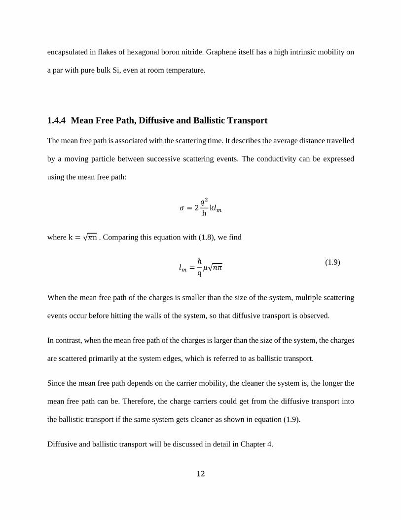
1.4.4 Mean Free Path, Diffusive and Ballistic Transport
The mean free path is associated with the scattering time. It describes the average distance travelled
by a moving particle between successive scattering events. The conductivity can be expressed
using the mean free path:
𝜎 = 2𝑞2
hk𝑙𝑚
where k = √𝜋n . Comparing this equation with (1.8), we find
𝑙𝑚 =
ℏ
q𝜇√𝑛𝜋
(1.9)
When the mean free path of the charges is smaller than the size of the system, multiple scattering
events occur before hitting the walls of the system, so that diffusive transport is observed.
In contrast, when the mean free path of the charges is larger than the size of the system, the charges
are scattered primarily at the system edges, which is referred to as ballistic transport.
Since the mean free path depends on the carrier mobility, the cleaner the system is, the longer the
mean free path can be. Therefore, the charge carriers could get from the diffusive transport into
the ballistic transport if the same system gets cleaner as shown in equation (1.9).
Diffusive and ballistic transport will be discussed in detail in Chapter 4.

13
Bibliography
1. K. S. Novoselov, A. K. Geim, S. V. Morozov et al., Electric field in atomically thin carbon
films, Science, 306, 666 (2004).
2. Reproduced from website: http://grapheneindustries.com/?Products.
3. A. H. Castro Neto, F. Guinea, N. M. R. Peres, K. S. Novoselov, and A. K. Geim, The electronic
properties of graphene, Rev. Mod. Phys. 81, 109 (2009).
4. https://www.graphene-info.com/skeleton-uses-curved-graphene-its-new-supercapacitor-
based-energy-storage-system

14
Chapter 2:
Fundamentals of Extraordinary
Magnetoresistance
2.1 Theory of Extraordinary Magnetoresistance
Magnetoresistance (MR) is a physical property of a material, showing the tendency to change the
value of electrical resistance with an externally-applied magnetic field. It was first discovered by
William Thomson (Lord Kelvin) in 1856.
The extraordinary magnetoresistance (EMR) is a specific geometrical magnetoresistance effect. In
the literature there are two major structures of EMR devices: circular and rectangular. For this
dissertation, we focus on the circular structure. Since the circular EMR device typically has a
thickness that is significantly smaller than its diameter, we treat the system as a two-dimensional
system. The EMR device is typically constructed with a circular semiconductor having an
embedded circular metal shunt in the center.

15
Figure 2.1 Schematic of EMR device.
Four contacts are evenly spaced around the device: two are used as current source and drain (I),
and the other two are used for voltage measurement (V). The nonlocal resistance is defined as
𝑅 = 𝑉/𝐼, and the magnetoresistance is normalized so that 𝑀𝑅 = [𝑅(𝐵) − 𝑅0]/𝑅0,
where 𝑅(𝐵) is the resistance in a magnetic field perpendicular to the device, and 𝑅0 is the
minimal resistance at zero magnetic field.
2.1.1 Lorentz Force
The conductivity of the metallic shunt, 𝜎𝑚, is much larger than that of the semiconductor, 𝜎𝑠. At
zero magnetic field, the current prefers to run through the low-resistance central metal shunt in our
device and therefore bypasses much of the graphene (or other semiconductor material); as the
magnetic field is increased, the Lorentz force
𝐹 = 𝑞(𝐸 + 𝑣 × 𝐵) (2.1)

16
-where 𝐸 is the applied electric field, 𝑣 the drift velocity of the charge carriers, and 𝐵 the magnetic
field - gradually redirects current into the high-resistance graphene area, bypassing the metal shunt.
Hence, we see the MR increases with the magnetic field, and that the conductivity ratio of the
metal to the semiconductor 𝜎𝑚/𝜎𝑠 plays a key role in the magnitude of MR. This will be discussed
more in Section 2.4.
Figure 2.2 Simulation of electrical current in EMR device with zero field (left) and with high
magnetic field (right) by COMSOL Multiphysics. Colors represent the electric potential, red
means high and blue means low. Red arrows represent the current density, the larger the arrows
the higher density. Black contours represent the equipotential lines.
Looking further into the physics details: at zero magnetic field, the direction of the current is
parallel to that of the applied electric field which is normal to the equipotential surface of the metal
(the metal itself is effectively an equipotential due to its high conductivity), therefore, the current
runs into and passes through the metal shunt since its direction is normal to the interface. However,
in a magnetic field, the current is deflected around the shunt by the Lorentz force and its direction
is no longer parallel with that of the electric field. At sufficiently high magnetic field, the direction

17
of current becomes parallel with the metal-semiconductor interface, therefore, the current bypasses
the metal shunt in the center. Thus, the current is forced to travel through the more resistive
material around the shunt, leading to a magnetoresistance enhanced over the zero field resistance
by orders of magnitude.
2.1.2 Mathematical illustrations
In 1927, the Drude–Sommerfeld model for free electrons was developed principally by Arnold
Sommerfeld. This model describes the behavior of charge carriers in a metallic solid.
There are four assumptions:
(1) Free electron approximation: The electrons do not interact with the ions which are treated
as charge neutral in the metal, except in boundary conditions.
(2) Independent electron approximation: The interactions between electrons are ignored.
(3) Relaxation-time approximation: The electron probability of collision is inversely
proportional to the average time between collisions--the relaxation time 𝜏.
(4) Pauli exclusion principle: An electron can only occupy one quantum state of the system.
This Drude–Sommerfeld model can be applied in semiconductor and graphene as well, and it is
the basis of the following derivations.
The applied magnetic field 𝐵 is in the 𝑧 direction so 𝐵 = (0, 0, 𝐵), and the current 𝐼 is driven
through the sample from the lower-left contact in the x direction. And the electric field 𝐸 is in the
x-y plane: 𝐸 = (𝐸𝑥, 𝐸𝑦, 0).

18
In the relaxation time approximation, the drift velocity 𝒗 of charge carrier can be expressed in
equation:
𝑚(𝑑𝑣
𝑑𝑡+𝑣
𝜏) = 𝑞𝐸 + 𝑞𝑣 × 𝐵
(2.2)
where q is the charge of the carrier; m is its effective mass; and 1/τ is its relaxation (scattering)
rate; the right hand side of the equation is the expression of the Lorentz force.
We only consider the steady state of system, so there is no velocity change with time.
So 𝑑𝑣
𝑑𝑡=𝑑𝑣𝑥
𝑑𝑡=𝑑𝑣𝑦
𝑑𝑡= 0. And then the rest of the velocity components can be expressed by electric
field and the magnetic field as
𝑣𝑥 = 𝑞𝜏
𝑚(𝐸𝑥 + 𝑣𝑦𝐵)
(2.3)
𝑣𝑦 = 𝑞𝜏
𝑚(𝐸𝑦 − 𝑣𝑥𝐵)
(2.4)
With these two equations, we can only use 𝐸𝑥 and 𝐸𝑦 to express 𝑣𝑥 and 𝑣𝑦:
(1+
𝑞2𝐵2𝜏2
𝑚2)𝑣𝑥 = 𝑞
𝜏
𝑚𝐸𝑥 +
𝑞2𝐵2𝜏2
𝑚2𝐸𝑦
(2.5)
(1+
𝑞2𝐵2𝜏2
𝑚2)𝑣𝑦 = −
𝑞2𝐵2𝜏2
𝑚2𝐸𝑥 + 𝑞
𝜏
𝑚𝐸𝑦
(2.6)
Combine these two equations, and get their matrix form:
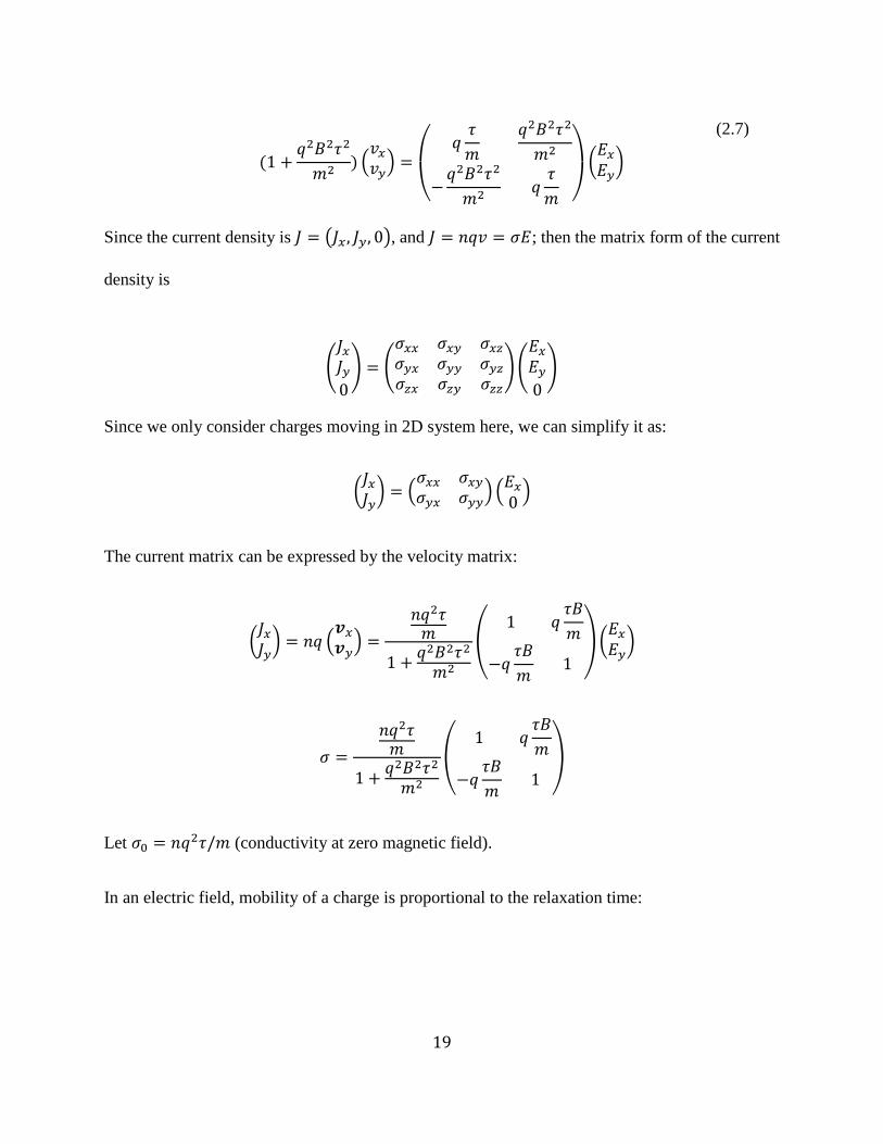
19
(1 +𝑞2𝐵2𝜏2
𝑚2) (𝑣𝑥𝑣𝑦) =
(
𝑞𝜏
𝑚
𝑞2𝐵2𝜏2
𝑚2
−𝑞2𝐵2𝜏2
𝑚2𝑞𝜏
𝑚 )
(𝐸𝑥𝐸𝑦)
(2.7)
Since the current density is 𝐽 = (𝐽𝑥 , 𝐽𝑦, 0), and 𝐽 = 𝑛𝑞𝑣 = 𝜎𝐸; then the matrix form of the current
density is
(𝐽𝑥𝐽𝑦0
) = (
𝜎𝑥𝑥 𝜎𝑥𝑦 𝜎𝑥𝑧𝜎𝑦𝑥 𝜎𝑦𝑦 𝜎𝑦𝑧𝜎𝑧𝑥 𝜎𝑧𝑦 𝜎𝑧𝑧
)(𝐸𝑥𝐸𝑦0
)
Since we only consider charges moving in 2D system here, we can simplify it as:
(𝐽𝑥𝐽𝑦) = (
𝜎𝑥𝑥 𝜎𝑥𝑦𝜎𝑦𝑥 𝜎𝑦𝑦
) (𝐸𝑥0)
The current matrix can be expressed by the velocity matrix:
(𝐽𝑥𝐽𝑦) = 𝑛𝑞 (
𝒗𝑥𝒗𝑦) =
𝑛𝑞2𝜏𝑚
1 +𝑞2𝐵2𝜏2
𝑚2
(1 𝑞
𝜏𝐵
𝑚
−𝑞𝜏𝐵
𝑚1
)(𝐸𝑥𝐸𝑦)
𝜎 =
𝑛𝑞2𝜏𝑚
1 +𝑞2𝐵2𝜏2
𝑚2
(1 𝑞
𝜏𝐵
𝑚
−𝑞𝜏𝐵
𝑚1
)
Let 𝜎0 = 𝑛𝑞2𝜏/𝑚 (conductivity at zero magnetic field).
In an electric field, mobility of a charge is proportional to the relaxation time:

20
𝜇 =𝑞
𝑚𝜏 (2.8)
Then 𝜎𝑥𝑥 =𝜎0
1 + 𝜇2B2 (2.9)
𝜎𝑦𝑥 =
𝜎0𝜇𝐵
1 + 𝜇2𝐵2
(2.10)
𝜎𝑦𝑦 = 𝜎𝑥𝑥 =𝜎0
1 + 𝜇2𝐵2 (2.11)
𝜎𝑥𝑦 = −𝜎𝑦𝑥 = −
𝜎0𝜇𝐵
1 + 𝜇2𝐵2
(2.12)
The conductivity components are expressed by the mobility and the magnetic field.
Thus, we can plug these components back to the conductivity tensor and get the final equation:
𝜎 = (𝜎𝑥𝑥 𝜎𝑥𝑦−𝜎𝑥𝑦 𝜎𝑥𝑥
)
=𝜎0
1 + 𝜇2𝐵2(1 −𝜇𝐵𝜇𝐵 1
)
= (
𝜎0
1+𝜇2𝐵2−
𝜎0𝜇𝐵
1+𝜇2𝐵2
𝜎0𝜇𝐵
1+𝜇2𝐵2𝜎0
1+𝜇2𝐵2
)
(2.13)
From this equation, we can see at B=0, 𝜎 is diagonal so J // E. At small B, the off-diagonal terms
of 𝜎 appears and make J non-parallel with E. At sufficiently high B, J is perpendicular to E since
the off-diagonal terms dominate.
The resistivity is the inverse of the conductivity: 𝜌 = 1/𝜎. So the resistivity tensor is also relevant
to the mobility of the device and the magnetic field as

21
𝜌 = (
𝜌𝑥𝑥 𝜌𝑥𝑦𝜌𝑥𝑦 𝜌𝑥𝑥
) =1
𝜎0(1 𝜇𝐵−𝜇𝐵 1
) (2.14)
where 𝜌𝑥𝑥 = 1/𝜎0 = 𝑚/𝑛𝑞2𝜏 and 𝜌𝑥𝑦 = 𝜇𝐵/𝜎0 = 𝐵/𝑛𝑞 . Therefore, we get the conductivity
tensor and resistivity tensor of the Hall effect.
2.2 First Discovery of Extraordinary Magnetoresistance
The EMR effect was discovered by Stuart Solin, et al. in 2000 [1]. Their EMR devices were
circular and made of a gold circular shunt in the center of an outside circular semiconductor InSb
(Indium antimonide) with 1.3-mm diameter, electron concentration n = 2.6 × 𝟏𝟎𝟐𝟐 𝒎−𝟑 , and
mobility μ = 4.55 𝒎𝟐/𝑽𝒔. Four evenly-spaced contacts are made by Ti/Pt/Au.
Figure 2.3 Schematic of EMR device made by Solin, et al. [1]
In this original discovery, the central metallic shunt has a much higher conductivity than the
semiconductor. An extremely large magnetoresistance, with R(B) at 9 T found to increase by more

22
than four orders of magnitude, arises due to the device geometry. And a huge magnetoresistance
of MR=15200 or a change of 1520000%, was also found in their EMR devices at room temperature.
They also demonstrated the metal shunt filling factor α, defined as α =𝑟𝑎
𝑟𝑏, can make a huge
difference in MR, where 𝑟𝑎 and 𝑟𝑏 are the inside and outside disk radii of the device. When the
filling factor is larger, more current runs through the central gold shunt of low resistance at zero
field; and correspondingly, more runs through the narrow area of the semiconductor of high
resistance at high field, yielding a larger MR increases. The filling factor α =12/16 or 13/16 has
been found to give the largest MR as shown by the solid circles in the plot below, and the filling
factor α = 0 (no metal shunt) gives almost negligible MR represented by the open square.
Increasing the filling factor beyond the optimal value, MR decreases since the semiconductor
channel is too narrow for a large current density.

23
Figure 2.4 Plot of MR versus the field of EMR device made by Solin, et al [1]. The solid circle
represents the largest MR corresponding to the filling factor α =12/16. And the open square
represents the smallest MR corresponding to the filling factor α = 0.
From this plot, we can see that MR starts at 0 at zero field and increases with the magnetic field.
The largest MR saturates at B=5T.
Since MR changes by four order of magnitude with increase of the B field to 5T, the EMR devices
show a very high sensitivity to magnetic field. The magnetic sensitivity represents how sensitive
the device is to the magnetic field, and it is defined as the derivative of resistance with respect to
the magnetic field, expressed as dR/dB. The high EMR effect suggests the EMR device can be
used to detect small magnetic field changes and therefore, EMR has received wide interests in
application of magnetic sensor and future hard drive [3].
Since its discovery, similar EMR devices have been made by different materials but none to date
rivals the largest record of magnetoresistance (MR) reported in Solin’s initial devices.
Practical EMR devices in industry such as magnetic sensors have rectangular structures since they
are easier to manufacture for use as microscopic field detectors, but there is a conformal
equivalence to the circular structures [4]. The rectangular structure is basically two unrolled strips
formed by semiconductor and metal.

24
Figure 2.5 Conformal mapping of EMR device [4]. Cut a circular EMR device with four equal-
spaced contacts and unroll the metal and semiconductor and get the rectangular structure of two
strips formed by semiconductor and metal. The resulting four contacts are equal spaced.
We note that Jian Sun et al. have used COMSOL Multiphysics to perform simulation in rectangular
devices and suggest that higher sensitivities could be obtained by using a two-contact EMR device
rather than a four-terminal measurement [7].
Figure 2.6 Schematic of the device and simulation of electric potential and sensitivity [7]. The
two current contacts are at the two ends of the device and the voltage contacts are in the middle.

25
In their device, the right current lead (I-) is set to ground potential so the potential at the right
corner is always zero. Therefore, the electrical potential is high at the left end and gradually
decreases to zero towards the right end of the device. We can conclude that if the two voltage
probes are infinitely close to the two current probes, the sensitivity becomes the largest. This
becomes equivalent to a two-contact rectangular EMR device.

26
2.3 Extraordinary Magnetoresistance in 2D
In a EMR device made of bulk materials, the material parameters are fixed and adjusting the
magnetic field is the only way to vary the EMR response. However, in a 2D EMR device, the
charge density of the system is tunable by an external electric field or gate voltage, so it gives a
new dimension of control over the MR besides the magnetic field, and the potential to realize
greater sensitivity.
One outstanding example of 2D material is graphene. Graphene based EMR devices has also
shown interesting magnetoresistance enhancement, with additional advantages of the tunable
charge density.
Figure 2.7 Schematic of graphene based EMR device
One of the first publications on graphene-based EMR device with a circular structure used
graphene grown by chemical vapor deposition with a central disk made of Ti/Au [4]. Due to its
polycrystalline nature, along with impurity residues from transferring CVD graphene from its
metal substrate to an oxidized wafer, the graphene devices have a low mobility of only
2500 𝑐𝑚2/𝑉𝑠. The largest EMR value achieved in their device is only around 6 (or 600%) at 12T

27
at room temperature, and the largest sensitivity is 145 Ω/T. These values pale in comparison to the
original InSb platform.
Figure 2.8 MR of the chemical vapor deposition grown graphene device. The colors represent
different gate voltages (in V). The inset is the sensitivity with respect to the gate voltage [4].
In the same year, a larger room-temperature MR enhancement of 550 (or 55 000%) at 9 T and a
larger two-probe sensitivity of 1600 Ω/T were reported using the mechanically exfoliated graphene
instead, in an EMR device with a central metal shunt of Ti/Au. These devices have a higher
mobility, varying from 4000 to 7000 𝑐𝑚2/𝑉𝑠 [5]. Their results were also explored using the
simulation performed in a finite element method software, COMSOL.

28
Figure 2.9 Schematic (a) and scanning electron microscope image with fake color (b) of the
exfoliated graphene based EMR device [5]. The contact configurations of the EMR measurements
of Solin’s device, the chemical vapor deposition grown graphene device and the exfoliated
graphene device are the same.
The authors also show increasing mobility can further increase MR in calculation.
Figure 2.10 Calculated MR vs the magnetic field in different mobility [5]. The MR increases by
around a half when the mobility gets doubled.
To understand the effect of the mobility on MR, we need to review the equation (2.13), which is
the conductivity tensor of the graphene in this case:
𝜎 =
(
𝜎01 + 𝜇2𝐵2
−𝜎0𝜇𝐵
1 + 𝜇2𝐵2
𝜎0𝜇𝐵
1 + 𝜇2𝐵2𝜎0
1 + 𝜇2𝐵2 )
At the high field, the diagonal components of the tensor become negligible and the off-diagonal
components dominate. We take one component as an example: 𝜎𝑦𝑥 =𝜎0𝜇𝐵
1+𝜇2𝐵2≈
𝜎0
𝜇𝐵 at high field.
When the mobility 𝜇 increases at a given field, the conductivity component 𝜎𝑦𝑥 decreases, and the

29
resistance of the sample increases. This causes the MR to increase at the high field since the zero-
field conductivity 𝜎0 should be the same.
Thus, this finding leads us to use encapsulated graphene with much higher mobility in EMR
devices, see if graphene can rival or even exceed the state-of-the-art in EMR.
2.4 More Simulations on Extraordinary Magnetoresistance
In 2012, Thomas H. Hewett and Feodor V. Kusmartsev have published an interesting simulation
paper on extraordinary magnetoresistance. Their simulation is also based on software COMSOL
Multiphysics. The models are based on Solin’s device: a circular semiconductor InSb embedded
with a central metal Au disk [7].
According to the simulation, MR increases with the conductivity ratio of the metal to the
semiconductor 𝜎𝑚 /𝜎𝑠 . Since 𝜎𝑚 determines the resistance at zero field and 𝜎𝑠 determines the
resistance at high field, the larger their ratio is, the larger MR is. The optimal ratio from the
simulation is 2430, and MR does not get significantly improved by further increasing the
conductivity ratio. Additionally, they also demonstrated that MR increases with the mobility of
the semiconductor.

30
Figure 2.11 Simulated MR vs the magnetic field in different conductivity ratios (left) and
mobilities (right) [7].
The contact resistance between the semiconductor and the metal can also impact the MR. In these
simulations, MR is the largest without contact resistivity, and begins to decrease as the contact
resistivity increases, because the large contact resistivity in the interface between the
semiconductor and the metal can impede the current from running through the metal shunt, even
at zero magnetic field.

31
Figure 2.12 Simulated MR vs the magnetic field in different contact resistivities [7].
In a second work on simulation of MR devices, the same authors claimed a multibranched
geometry can gives four order of magnitude larger MR than that of the circular geometry with the
same materials [2]. We can see the current get squeezed into very narrow channels in 6 locations
in the multibranched geometry at high field, contributing to the very large resistance. This
multibranched geometry has yet to be studied carefully.

32
Figure 2.13 Simulated MR vs the magnetic field in a multibranched geometry and a circular
geometry (left) and current distribution in the two geometries at zero field and 5 T (right). The
background color in the right figures represents the electric potential: brown means high, and blue
means low [2].
As for the 2D EMR device, besides the multibranched geometry, Solin et al. have shown that in
their simulation, a 10 𝜇𝑚 2D square structure with a square metallic inclusion in the center can
give a MR up to 105 (or 107 percent) for an applied magnetic field of 1 T [8]. This square
geometry could be also considered in the future EMR experiment.

33
Figure 2.14 A schematic for a 10 𝜇𝑚 square EMR device with contacts centered (left) and its MR
vs magnetic field for the central metal square of different sizes (right). The dashed lines represent
the MR for negative values of the magnetic field [8].
Bibliography
1. S. A. Solin, Tineke Thio, D. R. Hines, J. J. Heremans, Enhanced Room-Temperature
Geometric Magnetoresistance in Inhomogeneous Narrow-Gap Semiconductors, Science, 289,
1530 (2000).
2. T. H. Hewett and F. V. Kusmartsev, Geometrically enhanced extraordinary
magnetoresistance in semiconductor-metal hybrids, Physical Review B 82, 212404 (2010).
3. S. A. Solin, Magnetic Field Nanosensors, Scientific American, 291, 45 (2004).
4. A. L. Friedman, J. T. Robinson, F. K. Perkins, P. M. Campbell, Extraordinary
magnetoresistance in shunted chemical vapor deposition grown graphene devices. Appl.

34
Phys. Lett. 99, 022108 (2011).
5. Lu, J. et al., Graphene magnetoresistance device in van der pauw geometry, Nano Lett. 11,
2973 (2011).
6. Jian Sun, Chinthaka P. Gooneratne, Jürgen Kosel, Design study of a bar-type EMR device,
IEEE Sensors Journal, 12, 1356 (2012).
7. T. H. Hewett and F. V. Kusmartsev, Extraordinary magnetoresistance: sensing the future,
Cent. Eur. J. Phys., 10, 602 (2012).
8. Lisa M. Pugsley, L. R. Ram-Mohan, and S. A. Solin, Extraordinary magnetoresistance in
two and three dimensions: Geometrical optimization, Journal of Applied Physics 113, 064505
(2013)

35
Chapter 3:
Extraordinary Magnetoresistance in
Encapsulated Graphene Device
The discovery of the extraordinary magnetoresistance (EMR) effect by Solin and coworkers has
led to widespread interest in using this phenomenon for magnetic sensing applications [1-3].
On the other side, the advent of graphene in 2004, having tunable and bipolar conductivity, was
soon followed by a first generation of graphene-based EMR devices [3-5]. These were built from
graphene supported on SiO2, either by mechanical exfoliation or grown by chemical vapor
deposition. While a sizable EMR effect was achieved, these devices have generally fallen well
short of their semiconductor counterparts.
Recently, significant improvement in graphene devices has been realized through the
encapsulation of graphene in flakes of hexagonal boron nitride (hBN), an atomically-flat 5 eV gap
insulator with a honeycomb lattice alternately arranged by B atoms and N atoms [6]. hBN has a
layered structure similar to the graphene lattice, and it can be easily exfoliated into thin 2D layers,
even down to monolayer. Weak van der Waals forces that combine the hBN interlayers can be
used to make the heterostructure with graphene.

36
Figure 3.1 Schematic of honeycomb lattice structure of boron nitride.
In encapsulated graphene devices, the hBN protects the graphene from extrinsic sources of
disorder including e.g. water and adsorbed hydrocarbons, and much higher quality transport is
achieved [7]. Since increased device mobility has been linked to an enhanced EMR as show in
Section 2.4, it may be worthwhile to investigate EMR devices using encapsulated graphene.
Here we fabricate EMR devices based on flakes of monolayer graphene sandwiched between hBN
flakes, each approximately 30 nm thick. Monolayer graphene and hBN are exfoliated onto
oxidized silicon wafer chips and then assembled into stacks using a dry-transfer technique [8]. The
device geometry is defined by reactive ion etching to create a disk with outer radius 𝑟𝑏, and a
concentric circular hole with radius 𝑟𝑎 is also removed. Electrical contacts are made by depositing
a 4/80-nm-thick layer of Ti/Al, yielding several voltage and current leads at the external disk edge,
and the central metal shunt that connects to the entire inner perimeter. For uniformity, up to several
devices were made from a single graphene/hBN stack, as shown in Figure 3.2 (a). Electronic
transport measurements in both two- and four-terminal configurations were performed at 300 K in

37
a Quantum Design PPMS with a 9 T magnet. A gate voltage, 𝑉𝑔, applied to the conducting Si
substrate is used to control the carrier density and hence conductivity of the graphene. Devices are
made with varying ratios of the metallic shunt to outer radius, so that 𝑟𝑎/𝑟𝑏 = 0 corresponds to a
graphene device without the metal shunt and 𝑟𝑎/𝑟𝑏 = 1 corresponds to a pure metal disk without
graphene.
Figure 3.2 (a) Microscope image of a set of three devices fabricated from a single graphene/hBN
stack. Contacts and central metallic shunt are made by edge contacts to exposed graphene.
Schematic shows side view of device geometry. (b) Magnetoresistance, 𝑀𝑅 = [𝑅(𝐵) − 𝑅0]/𝑅0],
for the device with highest observed EMR effect at room temperature. The MR shows a strong
dependence on back gate voltage. (c) The as-measured (un-normalized) resistance for the same
gate voltages as in (b). The resistance itself shows little change with 𝑉𝑔. (d) The sensitivity, dR/dB,
for the same device, at 𝑉𝑔 = − 4.2𝑉. The red (cyan) trace was calculated from data measured in a
four- (two-) terminal configuration. Note the log-scale of the B-field axis.

38
Figure 3.2 (b) shows the normalized magnetoresistance, 𝑀𝑅 = [𝑅(𝐵) − 𝑅0]/𝑅0], from the device
having the highest observed EMR effect, for three closely spaced gate voltages which nonetheless
exhibit a remarkable variation in magnitude of the EMR. In contrast the measured resistance, 𝑅(𝐵),
for the same three traces is shown in Figure 3.2 (c) where, at least for positive magnetic field, the
resistances overlap almost identically. Thus, the variation in MR must be due to changes in the
value of 𝑅0(𝑉𝑔).
Typically, circular EMR devices are measured using four contacts spaced at 90 degree relative to
each other, but in this case device design constraints or poor electrical contacts led us to use four
neighboring contacts on one side of each device instead. Moreover, the metallic shunt is not always
concentric with the outer device radius. These features are known to lead to asymmetry in the
EMR [9], and are likely responsible for the observed asymmetry between positive and negative
magnetic fields in these traces, as shown in Figure 3.2 (b) and (c).
While MR is a standard figure-of-merit for EMR devices, it depends on the value of 𝑅0 which, in
these devices, is strongly dependent on the applied gate voltage. Yet the variation of resistance
when a field is applied is the quantity we are most interested in, particularly as R(B) is strongly
non-linear, and much of the field response occurs over the lowest one or two teslas. Thus, in
addition to plotting the MR, we also plot in Figure 3.2 (d) the sensitivity, or dR/dB, that has also
used to characterize the EMR response [4, 5, 10]. Here we discover that the sensitivity of
encapsulated graphene can greatly exceed that of graphene-on-oxide devices.
In particular, Figure 3.2 (d) shows the sensitivity calculated for the same device at 𝑉𝑔 = −4.2𝑉,
taking the derivative for data measured in a four-terminal configuration, and also for the same
39
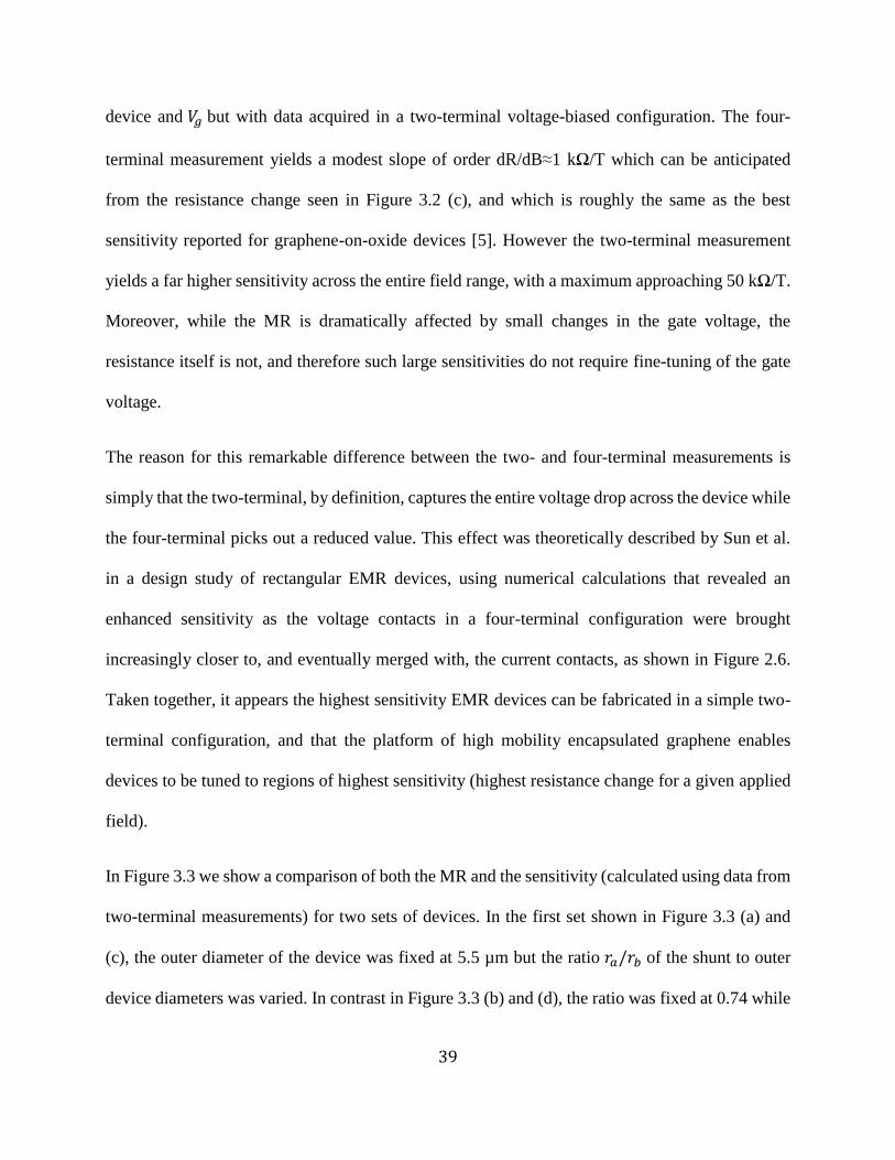
device and 𝑉𝑔 but with data acquired in a two-terminal voltage-biased configuration. The four-
terminal measurement yields a modest slope of order dR/dB≈1 kΩ/T which can be anticipated
from the resistance change seen in Figure 3.2 (c), and which is roughly the same as the best
sensitivity reported for graphene-on-oxide devices [5]. However the two-terminal measurement
yields a far higher sensitivity across the entire field range, with a maximum approaching 50 kΩ/T.
Moreover, while the MR is dramatically affected by small changes in the gate voltage, the
resistance itself is not, and therefore such large sensitivities do not require fine-tuning of the gate
voltage.
The reason for this remarkable difference between the two- and four-terminal measurements is
simply that the two-terminal, by definition, captures the entire voltage drop across the device while
the four-terminal picks out a reduced value. This effect was theoretically described by Sun et al.
in a design study of rectangular EMR devices, using numerical calculations that revealed an
enhanced sensitivity as the voltage contacts in a four-terminal configuration were brought
increasingly closer to, and eventually merged with, the current contacts, as shown in Figure 2.6.
Taken together, it appears the highest sensitivity EMR devices can be fabricated in a simple two-
terminal configuration, and that the platform of high mobility encapsulated graphene enables
devices to be tuned to regions of highest sensitivity (highest resistance change for a given applied
field).
In Figure 3.3 we show a comparison of both the MR and the sensitivity (calculated using data from
two-terminal measurements) for two sets of devices. In the first set shown in Figure 3.3 (a) and
(c), the outer diameter of the device was fixed at 5.5 µm but the ratio 𝑟𝑎/𝑟𝑏 of the shunt to outer
device diameters was varied. In contrast in Figure 3.3 (b) and (d), the ratio was fixed at 0.74 while

40
the outer diameter was varied. In prior EMR studies, the MR is generally found to reach a
maximum for a shunt-to-outer diameter ratio of 3:4 [9], and on the whole this is what we see in
Figure 3.3 (a), along with the MR decreasing with the ratio. However, the trend of the sensitivity
data is precisely the opposite, namely, the smallest ratio yields the largest sensitivity. At first glance
this is surprising, but we note the MR is a four-terminal measurement and thus is sensitive to the
change in voltage at a pair of contacts located close to the metallic shunt, while the two-terminal
data from which the sensitivity is determined captures the potential drop through the entire device,
including regions far from the shunt.

41
Figure 3.3 The MR (a) and sensitivity (c) for devices with varying shunt-to-outer diameter ratios
but fixed outer diameter of 5.5 µm. The MR (b) and sensitivity (d) for devices with varying outer
diameter at fixed ratio 𝑟𝑎/𝑟𝑏 = 0.74 . Here all MR traces are measured in a four-terminal
configuration, while the sensitivity is calculated from data acquired in a two-terminal voltage-
biased measurement.
In a magnetic field, the charge carriers are deflected from the center of the shunt. The larger the
magnetic field is, the more charge carriers pass through the two sides of the device. However, in a
fixed magnetic field, the smaller the ratio is, the more charge carriers also pass through the two
sides, and thus, the measured resistance is higher since the two sides are the high-resistance
graphene area.
The data for varying the overall diameter is less conclusive. In Figure 3.3 (b) there is no clear
dependence of the MR on device size. The sensitivity is found to be largest for the smallest
diameter device, but it is the middle device that has the smallest sensitivity (and also smallest MR).
Encapsulated graphene devices can vary widely in quality. During the process in which the
hBN/graphene/hBN stack is assembled, it is common to find regions with bubbles, wrinkles, or
torn graphene. As much as possible we attempted to fabricate devices from the smooth regions,
but it is possible that some of the variation noted here arises from inhomogeneities, and also
asymmetry in the device fabrication (e.g. an off-center metallic shunt).
In conclusion, we have investigated the extraordinary magnetoresistance effect in encapsulated
graphene devices. We find the magnetoresistance is enhanced by over four orders of magnitude
from its zero field value in the best devices. We also find enhanced values of the sensitivity, dR/dB,
reaching values of 50 kΩ/T, which exceeds prior reports in graphene-based devices by a factor of

42
up to 30. Encapsulated graphene is thus a promising platform for high-sensitivity measurements
of magnetic fields using the EMR effect.
Note: The study on sensitivity is still a work in progress. The final form will be presented in the
paper to be submitted later. The title of the paper should be: Highly sensitive extraordinary
magnetoresistance in encapsulated monolayer graphene devices.
Bibliography
1. S. A. Solin, T. Thio, D. R. Hines, and J. J. Heremans, Science 289, 1530 (2000).
2. S. A. Solin, D. R. Hines, A. C. H. Rowe, J. S. Tsai, Y. A. Pashkin, S. J. Chung, N. Goel,
and M. B. Santos, Applied Physics Letters 80, 4012 (2002).
3. T. Hewett and F. Kusmartsev, Central European Journal of Physics 10, 602 (2012).
4. A. L. Friedman, J. T. Robinson, F. K. Perkins, and P. M. Campbell, Applied Physics Letters
99, 022108 (2011).
5. J. Lu, H. Zhang, W. Shi, Z. Wang, Y. Zheng, T. Zhang, N. Wang, Z. Tang, and P. Sheng,
Nano Letters 11, 2973 (2011).
6. Y. Kubota, K. Watanabe, O. Tsuda, and T. Taniguchi, Science 317, 932 (2007).
7. C. R. Dean, A. F. Young, I. Meric, C. Lee, L. Wang, S. Sorgenfrei, K. Watanabe, T.
Taniguchi, P. Kim, K. L. Shepard, and J. Hone, Nature Nanotechnology 5, 722 (2010).

43
8. L.Wang, I. Meric, P. Y. Huang, Q. Gao, Y. Gao, H. Tran, T. Taniguchi, K.Watanabe, L.
M. Campos, D. A. Muller, J. Guo, P. Kim, J. Hone, K. L. Shepard, and C. R. Dean, Science
342, 614 (2013).
9. S. A. Solin and T. Zhou, in International Conference on Solid State Devices and Materials
(The Japan Society of Applied Physics, 2001) p. 570.
10. J. Sun, C. P. Gooneratne, and J. Kosel, IEEE Sensors Journal 12, 1356 (2012).

44
Chapter 4:
P-N Junction:
Theory, Experiment and Simulation
4.1 Basics of P-N Junction
An intrinsic semiconductor has no impurities and should have a balance of positive charges (holes)
and negative charges (electrons). Additional charges can be added when the impurities (dopants)
are introduced into a semiconductor. In a doped or extrinsic semiconductor, the number of the
positive charges and the number of negative charges are generally not equal any more. The p-type
semiconductor has larger hole concentration than electron concentration, and the n-type one has
more electrons than holes.
When a p-type semiconductor and a n-type semiconductor join, electrons near the p-n interface
diffuse into the p region and combine with holes leaving behind positively charged ions which
cannot move in the n region, and eventually form a negatively charged region in p region. In the
same way, holes near the interface diffuse into the n region and leaves the negatively charged ions
in the p region, and eventually form a positively charged region in n region. A strong electric field
appears near the interface due to the unbalanced charges, which counterbalances the diffusion of

45
both types of charges. Eventually the two opposite charged regions near the interface reaches the
equilibrium state, and a p-n junction is formed.
Figure 4.1 Schematic of a p-n junction and its electric potential.
The p-n junction is widely used as diode in industry, which only allows current to move in one
direction since the electric potential difference in the junction blocks electrons to move to a lower-
potential region. We can also understand this effect as the electric field in the junction stops the
electrons from moving to its opposite direction.
4.2 Metal-graphene Junction
Graphene has many properties in common with semiconductors. After graphene gets into contact
with the metal, charge doping from the metal changes the electric potential and charge density of
graphene in the contact area. Therefore, a metal-graphene junction is formed.
There are two types of metal-graphene contacts: surface contact and edge contact. The surface
contact is an area contact, but the edge contact occurs only along a line since graphene is a one-
atom-thick 2D material.

46
Figure 4.2 Schematic side view of surface contact and edge contact between graphene and metal.
4.2.1 Surface Contact between Graphene and Metal
When the metal surface contacts is made with graphene, for several metals Al, Ag, Cu, Au and
Pt(111) the surfaces have only physisorption to the graphene so the bonding is weak and the
electronic structure of graphene does not change. Certain other materials including Co, Ni, Pd, and
Ti surfaces, however, covalently bind and interact more strongly with graphene due to
chemisorption, and can perturb the electronic structure of graphene significantly [1]. When the
metal meets graphene, charges transfer between them due to the differences of their work functions
(in the simplest picture), and graphene get either n-doped or p-doped. Adsorption of graphene on
Al, Ag, Cu, Co, Ni, Pd (111) and Ti (0001) surfaces lead to n-type doping, while Au and Pt (111)
substrates lead to p-type doping of graphene.

47
Figure 4.3 Schematics of a graphene partly in contact with a metal showing the potential shift
caused by the charge transfer [1]. The upper plot shows two separate graphene: the graphene on
the metal surface is n-doped in this case, and the graphene far away from the metal is still free
standing and unperturbed. The lower plot shows when the two graphene pieces connect, the
rearrangement of the charges give rise to the potential shift and band bending.
In a paper by Xia and Avouris, et al., it was further reported that charge doping from surface-
contact metal can even cause asymmetries in the traces of resistance [2].
The metal contacts made by palladium and gold dope both the graphene underneath them and over
a short range into the graphene channel (that is not covered by metal) close to the contacts due to
direct contact and interaction between palladium and graphene. However, the applied gate voltage
can change the carrier type in the graphene channel far from the contact. For example, a metal that
n-type dopes graphene will lead to a pn-junction when the bulk of the graphene is gated to p-type
conduction.
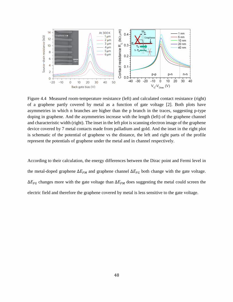
48
Figure 4.4 Measured room-temperature resistance (left) and calculated contact resistance (right)
of a graphene partly covered by metal as a function of gate voltage [2]. Both plots have
asymmetries in which n branches are higher than the p branch in the traces, suggesting p-type
doping in graphene. And the asymmetries increase with the length (left) of the graphene channel
and characteristic width (right). The inset in the left plot is scanning electron image of the graphene
device covered by 7 metal contacts made from palladium and gold. And the inset in the right plot
is schematic of the potential of graphene vs the distance, the left and right parts of the profile
represent the potentials of graphene under the metal and in channel respectively.
According to their calculation, the energy differences between the Dirac point and Fermi level in
the metal-doped graphene ∆𝐸𝐹𝑀 and graphene channel ∆𝐸𝐹𝐺 both change with the gate voltage.
∆𝐸𝐹𝐺 changes more with the gate voltage than ∆𝐸𝐹𝑀 does suggesting the metal could screen the
electric field and therefore the graphene covered by metal is less sensitive to the gate voltage.

49
Figure 4.5 Calculated energy differences as a function of gate voltage [2]. The red, green and blue
traces are for the graphene under the metal, and the grey trace is for the graphene channel without
the metal coverage.
The authors also demonstrated that the contact resistance is not sensitive to the different potential
profiles (linear, exponential, etc.) used in the calculation. Therefore, they used the exponential
profile
𝑈(𝑥) = 𝑈0
1
1 + 𝑒2 ln(3(𝑥/𝑊𝐵−1)) (4.1)
for their calculations. 𝑊𝐵 is the characteristic width over which the potential of graphene changes
by a half.

50
Figure 4.6 Calculated contact resistance as a function of gate bias using different potential profiles
with the fixed 𝑊𝐵=40 nm [2]. The inset are different potential profiles used in calculation.
They calculated the contact resistance as a function of the gate voltage for titanium-covered
graphene and showed the asymmetry of its trace is opposite to that of palladium-covered graphene.
In the titanium case, the n branch of the contact resistance is lower than its p branch. Therefore,
titanium induces n-type doping in graphene.
Figure 4.7 Calculated contact resistance vs the gate voltage for titanium-covered graphene [2].

51
4.2.2 𝝈 Bonds in Edge Contact and π Bonds in Surface Contact
In a theoretical paper published in 2014, Gao and Guo have shown that compared to the surface
contacts, graphene edge contacts can contribute to a much lower contact resistance due to their
shorter bonding distances, stronger overlaps of electron orbitals, and lower and narrower interface
barriers. The shorter binding distance leads to larger overlap between electron wavefunctions of
metal atoms and edge atoms, and therefore, the larger binding energy and the smaller interface
barrier height [3].
They used Ab initio density functional theory (DFT) calculations and non-equilibrium Green’s
functions (NEGF) simulations and demonstrated that different contact resistances can be achieved
in different edge terminations in the metal-graphene edge contact due to different binding distances,
overlaps of electron orbitals, and barriers across the interface from different chemical interaction.
Table 4.1 The binding distances and binding energies for Cr-graphene surface and edge contacts
with edge terminations indicated by X [3]. The Cr-C terminations are highlighted.

52
Dean et al. also claimed in the surface contact between graphene and metal, the lack of surface
bonding sites in π bonds on the surface of graphene causes the lack of chemical bonding, strong
orbital hybridization and large contact resistance [4]. Their experiments showed the contact
resistance for edge contacts can be remarkably low (as low as 100 ohm·µm in some devices) in
the 1D atomic edge of the encapsulated graphene in contact with the metal made by 1 nm Cr/15
nm Pd/60 nm Au, and the contact resistance is also asymmetric to the gate voltage: n branch of the
contact resistance is much lower than its p branch.
Figure 4.8 Calculated contact resistance vs the charge density (proportional to the gate voltage)
for two edge-contact graphene devices [4].
They also suggested that reactive ion etch process used in sample fabrication may bring some
additional interfacial species, such as oxygen, which can help to improve bonding and increase the
transmission of charges through the barrier of the contact resistance. They also showed that the

53
high mobility of graphene encapsulated by two boron nitride thin films can lead to ballistic
transport in graphene at 1.7K since the mean free path is greatly improved.
Figure 4.9 The plot of measured resistance vs gate voltage in a square encapsulated graphene
device at 300K and 1.7K [4]. The negative resistance at 1.7K suggest the charges get into the
ballistic transport regime.
Goddard et al., gave more details in the bonding of surface and edge contact [5]: In the surface-
contact graphene interfaces, only the π orbitals of carbon atoms contribute to the cohesion to the
surface metals; however, in the edge-contact metal-graphene interfaces, both the π orbitals and σ
orbitals contribute to the cohesion. Either unpaired (zigzag) or involved in a weakened in-plane π
bond (armchair), the σ electrons in the surface carbon atoms could play substantial roles in
cohesion and hence transmission of charges.
4.3 Experimental Discovery of Asymmetry in Gate-Voltage-
Dependent Resistance of Edge-Contacted Graphene

54
In principle an advantage of graphene-based EMR devices is the inherent tunability of graphene
via applying gate voltages to the substrate. In regular graphene devices without a shunt, the
resistance is a maximum at charge neutrality and falls off with increasing electron or hole charge
density; this is the so-called “Dirac peak” [7]. In shunted EMR devices made of graphene on oxide,
the resistance maximum survives but is rather broad [8, 9].
In contrast, in our encapsulated graphene EMR devices mentioned in Chapter 3 the resistance
maximum also survives but it invariably shows a strong asymmetry near charge neutrality; and
more importantly, the resistance can become negative. An example is shown in Figure 4.10, which
contains the zero-field resistance corresponding to the traces in Figure 3.2 (b), for devices with the
same ratio but varying outer diameters. In encapsulated graphene devices, the mean free path of
charge carriers can be of order 𝜇m even at room temperature [4], which is approximately the
spacing between the shunt and outer diameter of our devices. Thus transport in these devices is
nearly ballistic, and as a consequence “negative” resistances may arise due to geometric
resonances in scattering.

55
Figure 4.10 Asymmetry in the gate-voltage-dependent resistance at zero magnetic field and room
temperature, in three devices of varying diameters.
We compare the asymmetries in gate-voltage-dependent resistance at zero magnetic field and room
temperature in three different experiments, and see the asymmetries in the edge-contacted
graphene are much stronger than that in the surface-contacted graphene. This could arise from the
better overlap of the metal and carbon orbitals in the edge-contacted graphene than in surface-
contacted graphene, where the metal atoms encounter the graphene π orbitals that will not form
covalent bonds.
Experiment data of our EMR device Corry’s edge-contacted device Xia’s Surface-contacted device
Figure 4.11 Comparison of the asymmetries in gate-voltage-dependent resistance at zero magnetic
field and room temperature from tree different experiments.
4.4 Two Models
The metal shunt in our EMR graphene devices are composed of titanium and aluminum. The origin
of asymmetry in the zero-field resistance in our edge-contacted graphene devices arises from the
p-n junction that can occur at the interface of graphene with metals, especially titanium which

56
directly contacts graphene. This issue has been extensively investigated in the context of metallic
contacts to graphene devices.
Figure 4.12 Schematic of metal contacts and graphene on Si wafer (left) and photo of our EMR
device (right). The red circle on the right plot represents the titanium metal, which directly contacts
graphene.
According to Khomyakov et al., the work function of the free-standing graphene is 4.5eV, and
work function of the Ti-covered graphene is 4.17eV [1]. Since the work function of graphene is
given by the position of the Fermi level ( 𝑊 = −𝐸𝐹 ), Fermi energy of a free-standing graphene
is -4.5eV, and Fermi energy of the Ti-covered graphene is -4.17eV relative to the vacuum level.
Our models are based on edge-contacted graphene, and we expect the Fermi energy of graphene
at the contact interface of graphene and Ti should still be -4.17eV. Therefore, we can get the
schematic of the potential of graphene changing with the distance from the edge of the metal shown
in the picture below.

57
Figure 4.13 Schematic of the potential of graphene changing with the distance from the edge of
the metal. The black thick line is the profile of Dirac point.
Set the energy of the Dirac point as zero, we compare the energy difference between the Fermi
level and Dirac point (E=0):
Figure 4.14 Schematic of the energy difference between the Fermi level and Dirac point. The
energy difference decreases as the distance from the metal edge increases.

58
We use the finite element simulation software COMSOL. The details of this software and the
simulation are in the Appendix. To get the resistance or voltage between two voltage probes in the
device, we need to get the conductivity of the device for simulation. The process is shown below:
Potential Profile
=> Energy difference between Fermi level and Dirac point
=> charge density
=> conductivity of the device = conductivity (energy)
=> current or electric potential distribution in the device
=> resistance or voltage between two points in the device
We use the exponential profile given by Avouris et al. but do some modification to their equation
(4.1) to make it fit our case, the potential of graphene in our device is:
𝑃(𝑥) = 0.33 ×1
1 + 𝑒2 ln(
3(𝑥−𝑟)𝑊𝐵
) (4.2)
𝑟 is the radius of the circular metal disk. 𝑃(𝑥 = 𝑟) = 0.33 and 𝑃(𝑥 = ∞) = 0.
The exponential profile from our equation is plotted in Mathematica to confirm that it fits the plot
of energy difference between the Fermi level and Dirac point shown in the figure above.
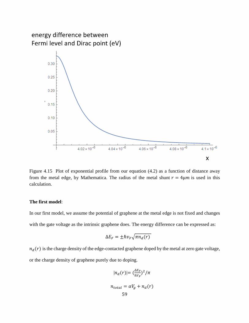
59
Figure 4.15 Plot of exponential profile from our equation (4.2) as a function of distance away
from the metal edge, by Mathematica. The radius of the metal shunt 𝑟 = 4µ𝑚 is used in this
calculation.
The first model:
In our first model, we assume the potential of graphene at the metal edge is not fixed and changes
with the gate voltage as the intrinsic graphene does. The energy difference can be expressed as:
∆𝐸𝐹 = ±ℏ𝑣𝐹√𝜋𝑛𝑑(𝑟)
𝑛𝑑(𝑟) is the charge density of the edge-contacted graphene doped by the metal at zero gate voltage,
or the charge density of graphene purely due to doping.
|𝑛𝑑(𝑟)|= (∆𝐸𝐹
ℏ𝑉𝐹)2/𝜋
𝑛𝑡𝑜𝑡𝑎𝑙 = 𝛼𝑉𝑔 + 𝑛𝑑(𝑟)

60
𝑛𝑡𝑜𝑡𝑎𝑙 is the total charge density of edge-contacted graphene doped by the metal at any gate
voltage, or the charge density of graphene considering both effects of doping and gate voltage.
The charge density of graphene is:
𝜎𝑔 = 𝑒𝜇|𝑛𝑡𝑜𝑡𝑎𝑙| + 𝜎𝑚𝑖𝑛
𝜎𝑚𝑖𝑛 = 4𝑒2/ℎ is the minimal conductivity of graphene.
𝜎𝑔 = 𝑒𝜇 |𝛼𝑉𝑔 + 𝑠𝑖𝑔𝑛(∆𝐸𝐹)(∆𝐸𝐹ℏ𝑉𝐹
)2/𝜋| + 4𝑒2/ℎ
where ∆𝐸𝐹=𝑊 −𝑊𝐺= 1
1+𝑒2 ln(
3(𝑥−𝑟)𝑊𝐵
)*0.33.
In the first model, ∆𝐸𝐹 = 𝑃(𝑥) as equation (4.2).
We can then put the equation of the conductivity into COMSOL for simulation.
The conductivity of graphene therefore can be expressed as a function of the distance from the
metal edge and the gate voltage.

61
Figure 4.16 The calculated conductivity as a function of distance at different gate voltages. 𝑊𝐵 is
the characteristic width over which the potential height changes by a half. Note: The radius of the
metal disk is set as 𝑟 = 𝑊𝐵 in my initial calculation. The general profiles of the conductivity traces
should be the same if r is changed to micron level (though the positions of the kinks would shift to
the right). The more accurate calculation will be provided in the second model.
In this figure, the conductivity changes with the gate voltage applied to the device. The red traces
represent the positive gate voltages, and the blue traces the negative voltages. Look at Figure 4.13,
positive gate voltages induces more electrons into the system, so the graphene near the metal edge
and far away from the metal forms a n-n junction, which does not limit the current, so its
conductivity is not small; the negative gate voltages, however, reduces the number of electrons or
induces the holes in the system, the graphene near the metal edge and far away from the metal

62
forms a n-p junction, of which the conductivity is small. Therefore, a kink appears in each blue
trace as the result of the absolute value of a negative value inside in the equation of 𝜎𝑔.
However, Song and Cho et al. use the capacitance experiments to demonstrate the work functions
of graphene under several metal electrodes such as Cr, Au, Pd, etc. are pinned or fixed no matter
what the gate voltage is. This gives us a different insight on the physics modeling of the metal-
graphene edge contact [6].
The second model:
In this model, the potential or work function of graphene in contact with the edge of the metal is
fixed or pinned, and does not change with the gate voltage since the electrons in a 3D metal do not
change with the gate voltage and therefore fix the electrons of graphene at the edge of the metal
too. On the other hand, the graphene far away from the metal is free-standing, so its potential
should be as that of the intrinsic graphene and free to move with the gate voltage.
The large density of states in the titanium metal contact serves to pin the Fermi level in graphene
so that it is highly doped (most metals yield n-type) near the contact. But out in the graphene bulk,
the carrier density may still be freely varied by application of a gate voltage. Thus for some range
of gate voltages, a p-n junction will arise near the contacts, serving to increase the effective contact
resistance. While the use of four-terminal measurements prevents this from appearing in resistance
measurements of uniform graphene devices, the effect of the metal shunt in the middle of our

63
devices is not removed, and the impact of pinning the Fermi level at the metal-graphene interface
ought to appear in the measurement.
To verify this picture, we have modeled transport through an EMR device, assuming an edge-
contacted geometry for the metallic shunt as sketched in the plot below.
Figure 4.17 Schematic of metal and edge-contacted graphene.
In models of surface-contacted graphene, the weak metal-graphene coupling allows the graphene
Fermi level to move in response to an applied gate voltage, even for graphene that is directly under
the metal [2]. In our edge-contacted graphene, we assume that covalent bonding at the graphene-
metal interface firmly pins the density in graphene at the interface, no matter what gate voltage
may be applied. At points in the graphene away from the interface, the potential relaxes back to
match the value in the bulk (e.g. set by the gate voltage) over a characteristic distance 𝑊𝐵.
In this model, Equation (4.2) is still correct but it does not represent the energy difference we seek
any more since we need to fix the energy difference at the metal edge. Therefore, we set the energy
difference as a linear function of the potential 𝑃(𝑥):
∆𝐸𝑓 = 𝑎𝑃(𝑥) + 𝑏
where a and b are constants.

64
According to the definition, at the metal edge: 𝑥 = 𝑟, 𝑃(𝑥 = 𝑟) = 0.33𝑒𝑉, so ∆𝐸𝑓 = 0.33𝑒𝑉 ×
𝑎 + 𝑏 = 0.33𝑒𝑉, suggesting the energy of graphene is fixed at the metal edge no matter what the
gate voltage is.
Far away from the metal: 𝑥 = ∞, 𝑃(𝑥 = ∞) = 0, so ∆𝐸𝑓 = 𝑏 = ∆𝐸𝑓𝑔, which is the energy of the
free-standing graphene depending on the gate voltage.
From these two equations, we can get
∆𝐸𝑓 = (1 −∆𝐸𝑓𝑔
0.33)𝑃(𝑥) + ∆𝐸𝑓𝑔
The electrical conductivity of which is represented by our mathematical equations:
𝜎 = 𝑒𝜇|𝑛| + 𝜎𝑚𝑖𝑛 (4.3)
|𝑛| = (∆𝐸𝑓
ℏ𝑣𝑓)2/𝜋 (4.4)
∆𝐸𝑓 = (0.33𝑒𝑉 − ∆𝐸𝑓𝑔)1
1+𝑒2 ln(
3(𝑥−𝑟)𝑊𝐵
)+ ∆𝐸𝑓𝑔 (4.5)
∆𝐸𝑓𝑔 = ±ℏ𝑣𝑓√𝜋𝛼|𝑉𝑔| (4.6)
Here, 𝑛 is the charge density, 𝜇 = 8𝑚2/𝑉𝑠 is the mobility used in simulation, 𝜎𝑚𝑖𝑛 = 4𝑒2/ℎ is
minimal conductivity of graphene, ∆𝐸𝑓 is the energy difference between the Fermi energy and the
Dirac point of graphene, ∆𝐸𝑓𝑔 refers to energy difference of graphene far away from the metal, 𝑣𝑓
is the Fermi velocity, 𝑊𝐵 is the characteristic width over which the potential height changes by
50%, x is the radius/distance away from the center of the device, r is the radius of the metal shunt,
𝛼 = 7 × 10¹⁰𝑐𝑚−2𝑉−1 is a constant, and 𝑉𝑔 is the gate voltage.
Therefore, the charge density and the conductivity can be both expressed as the distance (or radius)
and gate voltage. As the gate voltage increases from negative to positive, the charge density

65
increases. The traces of the charge density and the conductivity are very similar to each other
except those at the negative gate voltage because of the absolute sign in the conductivity equation.
Figure 4.18 Calculated charge density and conductivity as a function of the distance at different
gate voltages. The calculation is based on the characteristic width 𝑊𝐵 = 40 𝑛𝑚 and the radius of
the metal disk 𝑟 = 2.6 µ𝑚 same as that of the real device. The charge density and the
conductivity both are fixed at the metal edge, but gradually get more influnced by the gate voltage
as the distance from the metal edge increases.
The two figures above show the density and conductivity profiles for a range of gate voltages, in
a model device with 𝑟𝑎 = 2.6 µ𝑚. As expected, for gate voltages 𝑉𝑔 < 0 when the graphene bulk
is p-type, the conductivity reaches a minimum a short distance away from the graphene-metal
interface due to the appearance of a p-n junction. So, in Figure 4.10 the device resistance overall
reflects the fact that charge is less likely to traverse the metal shunt due to an effectively enhanced
contact resistance, and the remaining path around the shunt is through the more resistive graphene.
8
6
4
2
0
-2
n
( 1
01
2cm
-2 )
2.702.682.662.642.622.60
Radius ( m )
-40 -20 0 20 40
Vg (V)0.10
0.08
0.06
0.04
0.02
0
(
-1)
2.702.682.662.642.622.60
Radius ( m )
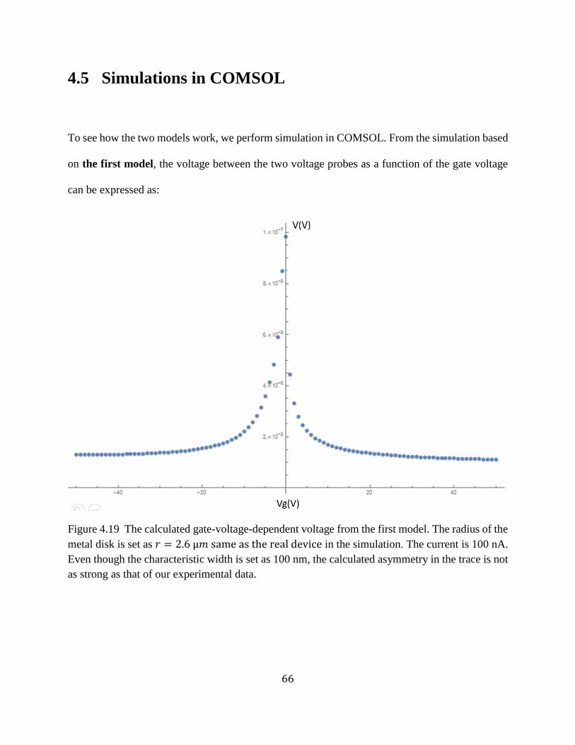
66
4.5 Simulations in COMSOL
To see how the two models work, we perform simulation in COMSOL. From the simulation based
on the first model, the voltage between the two voltage probes as a function of the gate voltage
can be expressed as:
Figure 4.19 The calculated gate-voltage-dependent voltage from the first model. The radius of the
metal disk is set as 𝑟 = 2.6 µ𝑚 same as the real device in the simulation. The current is 100 nA.
Even though the characteristic width is set as 100 nm, the calculated asymmetry in the trace is not
as strong as that of our experimental data.

67
Since the current is a fixed value, the asymmetry in the voltage reflects that in the resistance. Even
though asymmetry appears in this calculated trace, the asymmetry is not strong as our experimental
data suggests.
Since the doping from the metal shifts the Fermi level of graphene, the Dirac point of the doped
graphene should not be at zero gate voltage as that of the intrinsic graphene. We adjusted the
equation to shift the Dirac point to –10V which is the value I saw a lot in my previous graphene
devices.
Figure 4.20 Calculated voltage as a function of the gate voltage from the first model with Dirac
point adjusted.

68
A stronger asymmetry appears after shifting the Dirac point away from zero gate voltage. Thus,
the electron-hole asymmetry in the gate-dependent voltage (or resistance) is dependent on the
doping of graphene in our first model: the asymmetry is much stronger in doped graphene than in
the intrinsic graphene.
However, by performing simulation based on the second model, we also get a stronger asymmetry
in the gate-voltage-dependent voltage.
Figure 4.21 The calculated gate-voltage-dependent voltage from the second model. The current is
100 nA. The characteristic width is set as 100 nm (same as the value used in the first model to
compare the result), the calculated asymmetry in the trace is comparable with that of our
experimental data.

69
Even though we haven’t adjusted the Dirac point in the equation of the second model, the trace
still has a strong asymmetry which resembles our experimental data in the way that the hole branch
is noticeably higher than the electron branch, and the electron side of the peak has a sharp decrease
with the gate voltage. Hence, we conclude the second model makes a better physics prediction
than the first model.
We use the second model to simulate the resistance as a function of the gate voltage at different
characteristic widths.
Figure 4.22 Calculated resistance as a function of the gate voltage at different characteristic widths.
Despite the simplicity of our model, a reasonable agreement with our experimental data in the
Figure 4.10 is achieved with the best results for W = 100 nm: a similar asymmetry appears, over a
gate voltage range not too much less than we observe. The asymmetry gets stronger as the
characteristic width increases. A large characteristic width leads to a large doped area in graphene,
and hence, a “longer” p-n junction.

70
Figure 4.23 Schematic of doped area (light blue) in graphene (silver) near the metal (yellow) edge
increases with the characteristic width. The whole area of graphene could be doped if graphene is
heavily doped while its radius is small.
The kinks in the conductivity traces shown in Figure 4.17 represent the lowest conductivity and
the highest resistivity as the major contributor to stop the current flow. The kinks move away from
the metal edge as the characteristic width increases, suggesting the doped area of graphene
increases and the intrinsic area decreases. If the radius of graphene is small, the kinks in the traces
could go to the end of the device or even out of the range which suggests the whole area of
graphene is doped.

71
In summary, we demonstrate that an asymmetry in the gate voltage response of the zero-field
resistance is traced to the presence of p-n junctions near the graphene-metal interface, and a model
of edge-contacted graphene is in reasonable agreement with these observations.

72
Bibliography
1. P. A. Khomyakov, G. Giovannetti, P. C. Rusu, G. Brocks, J. van den Brink, and P. J. Kelly,
First-principles study of the interaction and charge transfer between graphene and metals.
Physical Review B, 79, 195425 (2009).
2. F. Xia, V. Perebeinos, Y.M. Lin, Y. Wu, and P. Avouris, The origins and limits of metal–
graphene junction resistance, Nature Nanotechnology, 6, 179 (2011).
3. Q. Gao and J. Guo, Role of chemical termination in edge contact to graphene, APL
Materials, 2, 056105 (2014)
4. L. Wang and C. R. Dean et al., One-Dimensional Electrical Contact to a Two-Dimensional
Material, Science, 342, 614 (2013)
5. Y. Matsuda and W. Goddard III et al., Contact Resistance for “End-Contacted” Metal-
Graphene and Metal-Nanotube Interfaces from Quantum Mechanics, J. Phys. Chem. C,
114, 17845 (2010)
6. Seung Min Song, Jong Kyung Park, One Jae Sul, and Byung Jin Cho, Determination of
Work Function of Graphene under a Metal Electrode and Its Role in Contact Resistance,
Nano Lett., 12, 3887 (2012)
7. K. S. Novoselov, A. K. Geim, S. V. Morozov, D. Jiang, Y. Zhang, S. V. Dubonos, I. V.
Grigorieva, and A. A. Firsov, Science 306, 666 (2004).
8. A. L. Friedman, J. T. Robinson, F. K. Perkins, and P. M. Campbell, Applied Physics Letters
99, 022108 (2011).
9. J. Lu, H. Zhang, W. Shi, Z. Wang, Y. Zheng, T. Zhang, N. Wang, Z. Tang, and P. Sheng,
Nano Letters 11, 2973 (2011).

73
Chapter 5:
Conclusion
5.1 Summary
This dissertation explored the phenomenon of extraordinary magnetoresistance (EMR) and p-n
junction in boron nitride encapsulated monolayer graphene devices. Chapter 1 introduced the
fundamentals of graphene, especially its basic physical properties relevant to the experimental
results presented in Chapter 3. Chapter 2 switched to the topic of extraordinary magnetoresistance,
from the theory to its first discovery in 3D, and to EMR in 2D.
With enough background provided in Chapter 1 and 2, the experimental section began in Chapter
3. We performed room-temperature electrical transport measurements on gated encapsulated
monolayer graphene devices in a magnetic field up to 9T, and found the extremely large EMR
values and the largest reported values of the sensitivity to magnetic fields. In many devices the
zero-field resistance can be vanishingly small and even become negative due to ballistic transport.
We also explored the effects of the sizes of the devices and the ratios of metallic disk to graphene
on the EMR and sensitivity.
Chapter 4 first started with p-n junctions in the semiconductor and surface-contacted graphene,
which is followed by a discussion of 𝜎 bonds in edge contact and π bonds in surface contact. Then
it talked about my experimental data showing strong electron-hole asymmetry in gate-dependent
resistance at zero field results from a resistive p-n junction in the heavily electron-doped area of

74
graphene near the central metallic shunt. Two models were built to explain the physics behind the
asymmetry and led to calculation and simulation in COMSOL to verify the picture.
5.2 Outlook
There are still many new and interesting problems to address with EMR in edge-contacted
graphene. Figure 3.2 suggests the EMR and the sensitivity show the opposite dependence on the
ratio of the shunt to outer device diameters, however, both show no clear dependence on the device
size possibly due to inhomogeneities in graphene or off-center metallic shunt. These phenomena
could be experimentally explored more.
The experiments in this dissertation were performed at room temperature. I have also measured
the field-dependent resistance at 10K, which showed Shubnikov–de Haas effect. Since the
aluminum is a major component of the central metal shunt in our devices, and it is a type-I
superconductor with critical temperature 𝑇𝑐 = 1.2 K, what would happen to the EMR when the
aluminum is superconducting and has no resistance? Will EMR become much larger at a small
field 𝐻 < 𝐻𝑐 = 0.01T? Since the thickness of aluminum is 90 nm, the thin film aluminum could
remain superconducting in a field higher than 𝐻𝑐 because of the magnetic flux vortices. Any other
interesting phenomenon could be observed at such low temperature?

75
Figure 5.1 Magnetoresistances of EMR devices at 10K at different gate voltages.
Additionally, the gate-dependent resistance of my many other EMR devices show double humps
in their Dirac peaks. It could also result from the inhomogeneities in graphene. Although the
simulation in COMSOL that considered inhomogeneities in graphene gives a similar result, it still
needs more concrete evidence.

76
Figure 5.2 (Top) Gate-dependent resistances of EMR devices at different gate voltages. (Bottom)
Simulated gate-dependent resistance in COMSOL.
Besides the EMR project, I have four unfinished projects and very much hope to finish them. In
the project of spin-orbit coupling in graphene on HfO2, we hope graphene could inherit the strong
spin-orbit coupling from atomic-layer-deposited HfO2 in order to make graphene a 2D topological
insulator. This research has potential applications in topological insulator quantum supercomputer.
One device has been measured and many beautiful plots came out from it. Even though we didn’t
see the weak antilocalization in the weak localization measurements possibly because the HfO2 is
not clean enough to provide high mobility in graphene, 20 more devices I made are still waiting to
be measured.

77
Figure 5.3 (Left) Landau fan diagram of graphene-on-HfO2 devices at 10K. The color represents
the resistance. (Right) Weak localization measurements at different temperatures.
In the germanium telluride (GT) project, our goal is to experimentally confirm the ferroelectricity
is largely enhanced in GT thin film, as suggested by theoretical work of Li Yang’s group in our
department. This project has applications in ferroelectric capacitors, ferroelectric RAM and RFID
cards. One device of 30nm-thick GT was measured, and the resistance measurements vaguely
suggest there are gate and magnetic field dependences. Even though germanium telluride may not
be a layered material and is very hard to exfoliate to get thin films, I was still able to get some thin
films that could be but have not been measured yet.
12
10
8
6
4
2
0
B(T
)
-40 -20 0 20 40
Vg(V)
020416_a1.004
ln(Rxx)
11
10
9
8
7
6
5
-40
-30
-20
-10
0
x1
0-3
[R
-R(B
=0
)] / R
(B=
0)
0.100.050.00-0.05-0.10
B(T)
dr_008: 4K dr_040: 8.2K dr_041: 9.3K dr_043: 12.2K
WL at different temperatures Vg=+17V
-1.2
-1.0
-0.8
-0.6
-0.4
-0.2
0.0
V(m
V)
120100806040200
T7 (K)
Vxx(14-15)_001 Vxy(14,5)_001

78
Figure 5.4 (Top Left) Microscopic image of germanium telluride thin film device. (Top Right)
The voltages across the device versus the temperature (the kink in blue trace is an error in
sensitivity of lock-in). (Bottom) Its resistances versus the gate voltage and magnetic field.
In the project of periodic-lattice electrical potential on encapsulated graphene, we aim to use the
periodic-lattice electrical potential to artificially induce a superlattice in graphene. The holes in
the top boron nitride film were drilled by focused ion beam, and two new devices have been
made but never get a chance to get measured.
Figure 5.5 (Left) The schematic of encapsulated graphene devices with the top boron nitride films
with periodic-lattice holes filled by metal. (Right) Atomic force microscope image and profile of
the holes.
500
400
300
200
R(k
½)
40200-20-40
Vg(V)
R_003 (3-12) R_004 (5-12) R_005 (5-3)
360
340
320
300
280
260
240
220
R(k
½)
121086420
B(T)
R_006 at Vg=0 R_007 at Vg=45V

79
In the project of hydrodynamics of encapsulated graphene, we wish to use a more precise way to
experimentally confirm the viscosity of electrons in graphene studied in other papers. I made
several encapsulated graphene devices including monolayer graphene devices and bilayer
graphene devices, and collected some data showing the negative resistance which may be a sign
of viscous electrons. But I was switched to other projects and didn’t get a chance to finish this
project either.
Figure 5.6 (Top left) Microscopic image of encapsulated graphene device with a top gate. (Top
right) Top-gate-dependent resistance at different back gate voltages. (Bottom) Gate-dependent
resistance shows negative values.

80
Appendix A
Instruments and Techniques
The encapsulated graphene devices widely used in transport measurements are made by boron
nitride/graphene/boron nitride stacks. The boron nitride is an insulator with similar hexagonal
structure and can be exfoliated for flat and clean thin films. Use the boron nitride thin films to
encapsulate graphene and squeeze out the air between them can remove the hydrocarbon in the air
attached to graphene, which is a major source of contamination that compromise the carrier
mobility of graphene.
Figure A.1 Photo of boron nitride thin film (its light green color suggests its thickness is around
30nm).

81
The process of making encapsulated graphene device is:
(a) Make boron nitride/graphene/boron nitride stack.
(b) Spin coat the resist and use electron beam lithography to define the patterns of wires.
(c) Etch the stack to expose the edge of graphene.
(d) Deposition of metal wires to electrically connect graphene.
(e) Spin coat the resist and use electron beam lithography to define the geometry of the device.
This step can also happen before step (b).
(f) Etch the stack to get the desired geometry of the device.
Then we get the desired geometry of the device connected with the metal wires.
In the figures below, I use the Hall-bar device as an example. The process for making any device
is the same.
Figure A.2 Illustration of fabrication process of encapsulated graphene device.

82
The details of device fabrication and relevant instruments are shown in the following sections.
A.1 Probe Station and Stacking of Graphene
We use the probe station to transfer boron nitride film and graphene to make heterostructures.
Figure A.3 Photo of probe station (left) and the heater control (right).
A polypropylene carbonate (PPC) film coated soft and transparent gel-like polydimethylsiloxane
(PDMS) block mounted on a glass slide is used to pick up and drop down graphene and thin boron
nitride films to form van der Waals heterostructure.

83
The recipes for spin coating PPC:
(1) Prebake the substrate at 100 Celsius for 1 minute.
(2) Spin coat PPC.
(3) Post bake at 100 Celsius for 2 minutes.
The process of making boron nitride/graphene/boron nitride stack is shown below:
Figure A.4 Schematic of the process of stacking.
A.2 Scanning Electron Microscope and Electron beam
Lithography
A scanning electron microscope (SEM) is widely used in physics research and semiconductor
industry to characterize nanomaterials. SEM accelerates a beam of electrons to scan the surface of
the sample and interact with atoms within, generating various signals with information about the

84
surface topography and composition of the sample, and producing images of the sample. The
resolution of SEM can be better than 1 nanometer. In the most common SEM mode, the secondary
electrons emitted by atoms excited by the electron beam are detected.
After our graphene stack is made, the stack along with the surface of the substrate are spin coated
with two to three layers of transparent resist sensitive to the electron beam, called Poly(methyl
methacrylate) (in short, PMMA). The resist is used for writing pattern to help etch the sample into
the desired shape or deposit metal wires to electrically connect the graphene. For etching, two
layers of 950PMMA are good enough to protect the sample. For depositing metal wires, two layers
of 495PMMA and one layer of 950PMMA should be used. 495 and 950 represent 495,000 and
950,000 molecular weight respectively.
The recipes for spin coating PMMA are:
(1) Prebake the substrate at 150 Celsius for 1 minute.
(2) Spin coat 495PMMA and postbake at 150 Celsius for 2 minutes. And repeat this step as
needed.
(3) Spin coat 950PMMA and postbake at 150 Celsius for 2 minutes.
To help us locate the micrometer-size device on the centimeter-size substrate in optical microscope,
alignment marks are written/drawn in the PPMA by our Scanning Electron Microscope -- JEOL
JSM-7001 LVF Field Emission SEM with the help of a software called Nabity Electron Beam
Lithography (e-BL) pattern writing system (also called Nanometer Pattern Generation (NPGS)
System) which controls the beam to write pattern. The process is called electron-beam lithography.

85
Figure A.5 Photo of scanning electron microscope.
The solubility of the resist is changed by the electron beam, so the exposed regions of the resist
can be selectively removed by a developing process--immersing the chip in a cold solvent which
is the composition of Isopropyl alcohol (IPA) and deionized water (the ratio is 3:1).

86
Figure A.6 Photo of alignment marks in PMMA.
One advantage of using PMMA is that it can be rewritten for several time as long as it is not over-
exposed to the electron beam. We design the pattern we want for our sample in the NPGS system
and then use electron beam lithography to write the pattern on the PMMA. After development, the
ideal case for depositing metal wires is to get an undercut in the resist to help the lift off process
later. The reason why undercut appears is because the molecular weight of 495PMMA is around
a half of that of 950PMMA so it is dissolved faster in developer.

87
Figure A.7 Schematic of undercut in three-layer PMMA resist. The thickness of each layer of
PMMA is in micrometer-size level so the thickness of the real resist should be negligible compared
to the thickness of the substrate.
Figure A.8 Photo of EBL pattern in device. The purple color is the exposed regions of Si substrate,
and represents the pattern of wires written on the PMMA for metal deposition later.
A.3 Heidelberg Laser Writer
An alternative way to make pattern is to use the Heidelberg laser writer in our cleanroom. It is very
beneficial to use the laser writer for the large-scale patterns since it writes fast and saves a lot of
time. Another advantage of using the laser writer is no need of alignment marks as long as the

88
resist is transparent to the infrared light of the camera used to locate the sample. The experience
tells us that we can see the sample underneath if the resist surface is smooth.
Figure A.9 Photo of Heidelberg laser writer system.
The system we use is Heidelberg DWL66+ Laser writer. It concentrates the ultraviolet light with
a wavelength of 375 nm into a laser beam to pattern a single photoresist layer. It can be considered
as an advanced version of UV mask aligner that performs photolithography without using
photomask, instead it controls the location of UV beam to write patterns. The laser writer has two
laser heads: 10 millimeter head and 2 millimeter head. The laser spot size(diameter) of the 10
millimeter head is 2 micrometer, and that of the 2 millimeter head is 600 nanometer. So the

89
smallest feature size that can be written by the 2 millimeter head is around 600 nm. The resist
thickness can range from 100 nm to 100 µm.
The resist we use in the laser writer is KL IR Lift-Off 15 Dual-Tone Photoresist. It can be used
both as a positive resist and a negative resist. The negative resist mode is used for lift-off process.
Figure A.10 Scanning electron microscope image of the KL IR resist with undercuts [1].

90
KL IR patterning for Lift-off Process is:
(1) Spin coat at 5000 rpm (and get the thickness of 1.18 micrometer).
(2) Negative soft bake at 105 Celsius for 90 s.
(3) Laser writer exposure by 10 mm head: Focus 0, Power 70 mW, Filter 50%, Intensity 80%,
Exposure runs two times (optimized). Results: 2 um feature comes out to be close to 2 um.
Or
Laser writer exposure by 2 mm head: Focus 0, Power 47mW, Filter 12.5%, Intensity 100%
(optimized). Results: 2 um feature comes out to be 1.68 um.
(4) Post Bake (reversal bake) at 130 Celsius for 90 s -- Very critical step.
(5) Flood exposure by mask aligner in power of 150 mJ/𝑐𝑚2.
(6) Develop for ~45 seconds in MIF-319. Watch the pattern carefully to prevent over
development.
Note: there is a small difference in exposure parameters for writing on resist directly on silicon
substrate and on boron nitride film. The light reflection rates are different on the substrate and on
the boron nitride film, so the secondary exposure on the surrounding resist is different. Therefore,
it is a good idea to do test run in small scale first to optimize the exposure parameters before the
actual exposure, otherwise you may get a pattern wider than you expect.

91
One disadvantage of using laser writer is that it cannot draw clear patterns smaller than 1.68 um.
So we still have to use electron beam lithography when we want to have smaller patterns. Another
disadvantage of using this system is the drifting of the laser beam: we can see there is a
misalignment of a few micrometers between the pattern and the sample after ten-minute beam
exposure. The drifting is always happening independent of exposure, so the shorter time the
process takes, the smaller drifting you get.
When the patterns of the wires are drawn, the next step is deposition of metal.
A.4 Electron Beam Evaporator
The electron beam evaporator accelerates the electrons to bombard the metal source in a high
vacuum, and the heated metal atoms are transformed from solid state into gaseous phase and coated
on the substrate along with the chamber.

92
Figure A.11 Photo of electron beam evaporator system.
We use the AJA International e-beam instrument to deposit titanium (as an adhesion layer) and
aluminum in a very high vacuum ~1𝑒−9 torr.
The parameters we use in electron beam evaporation is:
Base pressure: 1.2 × 10⁻⁹ torr. Spin the sample holder for uniform coating.
Titanium: 70 mA current, 1.4 Å/s evaporation rate, 4 nm thickness.
Aluminum: 190 mA, 2.4 Å/s, 80 nm.

93
Figure A.12 Photo of device with Al wires (white) made by electron beam evaporation.
Note: Every time the evaporation chamber gets open for repair, moisture and air get in it. We need
to wait for more than a week to pump down to low enough pressure (smaller than 2 × 10⁻⁸ torr)
before reuse, otherwise the lift-off could be very bad (you can see a lot of wrinkles appear on the
metal film after evaporation).

94
A.5 Thermal Evaporator
The thermal evaporation is also a way for metal deposition. It heats up the metal source to
evaporate and coat on the substrate. However, the edge-contact resistance of the device resulted
from thermal evaporation is huge, in megaohms, suggesting bad contacts. Our guess is the pressure
in the thermal evaporator cannot get low enough (the lowest pressure is ~10−6 millibar), so the
metal atoms to form contact get oxidized very quickly.
We only use thermal evaporator for non-edge-contact evaporation.

95
Figure A.13 Photos of Edwards auto 306 thermal evaporator. The lower photo is taken when the
evaporator is heating up and evaporating the gold source.
The parameters we use in thermal evaporation is:
Base pressure: 1.9 × 10⁻⁶ millibar.
Cr (adhesion layer): 3.8 A current, 1.5 Å/s evaporation rate, 4.5 nm thickness.
Au: 4 A, 4.7 Å/s, 90 nm.
After evaporation, we put the substrate into acetone at 50 Celsius for more than half an hour for
lift-off. If the undercut of the resist is in good shape, then lift-off process should not be hard.
According to my experience, the lift-off process after thermal evaporation is much easier than that
after electron beam evaporation.
And then, we perform spin coating process and the electron beam lithography process again to
write pattern for reactive ion etching.

96
A.6 Reactive Ion Etching
The wet etching could bring impurities to contaminate graphene since it uses liquid chemicals to
remove materials from a wafer, the dry etching is used to etch high-mobility graphene devices. We
use reactive ion etching, which generates plasma and drives high-energy ions to hit wafer surface
and chemically react with it. We use Oxford Plasma Lab 100 Inductively Coupled Plasma (ICP).
Figure A.14 Photo of reactive ion etching system.
The recipes I use for etching boron nitride/graphene/boron nitride stack is:
SF6 50 sccm and O2 5 sccm. RF power 100 W and ICP power 100 W. Pressure 50 mtorr. Etch 7
seconds for 60 nm-thick device.

97
Figure A.15 Schematic process of reactive ion etching and evaporation.

98
Figure A.16 Pictures of device before and after etching. The Au top gate (yellow) was made by
the thermal evaporation.
A.7 Physical Property Measurement System
The measurement system we use is the Physical Property Measurement System (PPMS), which
consists of a 9-tesla superconducting magnet in a helium dewar with sample temperature range
from 2K to 400K. It is like a small version of dilution refrigerator, and it has advantages such as
easier operation, faster cool down rate and faster ramp rate of the magnet compared to the dilution
refrigerator. The downsides of using PPMS are the minimal ramp rate of its magnet is still too fast

99
to get high-resolution 3D plots of R vs Vg and B when we simultaneously sweep the gate voltage
and the magnet, so we have to sweep the magnet back and forth several times to compensate it.
Figure A.17 Picture of PPMS and measurement instruments.
Bibliography
1. KL IR resist image reproduced from website: http://micromaterialstech.com/wp-
content/uploads/2015/06/Image-Reversible-Resist-LiftOff-ver2.pdf

100
Appendix B
Measurement Circuit
Before the transport measurements, we measure the contact resistances (the resistances of contacts
between the metal and graphene) first to make sure enough contacts working for our measurements.
The circuit diagram for contact resistance measurements is shown below:
Figure B.1 Circuit diagram for contact resistance measurement.
Voltage divider 100:1 is used to transform the output voltage 20 mV into 0.2 mV or 200 µV.
𝑅𝑉 is variable resistor.
𝑅𝐶 is contact resistance of graphene device.
𝑉𝑚 is the measured voltage.

101
Only one contact of the graphene device is connected in series with the variable resistor and all
the rest are grounded so that only one contact resistance is measured each time. The current is
same in the same metal wire, so the current runs through 𝑅𝐶 and 𝑅V is the same:
200𝜇𝑉 − 𝑉𝑚𝑅𝐶
= 𝐼 =𝑉𝑚𝑅𝑉
Then the contact resistance can be expressed as the measured voltage and resistance used in the
variable resistor as
𝑅𝐶 =200𝜇𝑉 − 𝑉𝑚
𝑉𝑚𝑅𝑉
When the variable resistor is adjusted so that the measured voltage is a half of the voltage provided
(200 𝜇𝑉 in this case), the voltages across the variable resistor and the contact should be the same,
then the contact resistance is equal to the resistance in the variable resistor. This is how we found
the contact resistance.
After the contact resistance measurements, we perform the four-wire transport measurements. We
use EMR measurement as an example:

102
Figure B.2 Circuit diagram for 4-wire resistance measurement
𝑅𝑔 is the measured resistance of graphene.
𝐼𝑚 is the measured current.
The circuit diagram is similar to that of contact resistance measurement. In the 4-wire resistance
measurement there is no variable resistor, and we directly measure the voltage across two contacts
of the graphene device and the current running through the device. So the resistance of the device
is 𝑅𝑔 = 𝑉𝑚/𝐼𝑚.

103
Appendix C
Contact Resistance
From my experience, the contacts with resistance smaller than 10K ohms are good for
measurements and those with resistance larger than 10K ohms could have large noise in signal.
And the larger the contact resistance is, the larger the noise is, and the less usable the contact is.
I have made around eighty graphene devices, many of them have only three contacts with small
contact resistance and others with huge contact resistance (some of them have mega ohms). I have
tried many ways to solve this problem, but none of them seem to work until I made contact
interface between the metal and the graphene wider.
Figure C.1 Photos of devices before I made contact area larger. Each red mark suggests one
working contact while the rest are bad contacts.

104
After I made those contact areas larger, the number of working contacts get statistically improved:
most contacts of each device work. The reason is simple: the contact interface between 2D
graphene and 3D metal is only a 1D line. So the contact resistance is inversely proportional to the
contact width. The wider the contact width is, the smaller the contact resistance is.
Figure C.2 Schematics of the 3D and 2D contact interfaces.
Below is an example of comparison of wide contact interfaces and narrow contact interfaces, the
Al wires and the graphene contacts were intentionally made wider in the left figure to make the
contact interfaces wider:

105
Figure C.3 Schematics of the wide (left) and narrow (right) contact interfaces. The interfaces are
shown in red color.
Figure C.4 Photos of devices after I made contact area larger.

106
Another way to make contact resistance smaller is to use the Heidelberg Laser Writer to write the
wiring patterns before evaporation, and most of the contacts work without widening the contact
interfaces. It is likely that the undercut of the single-layer KL IR resist is not as wide as that of the
three-layer PMMA resist.
Figure C.5 Schematics of the undercuts of PMMA resist and the KL IR resist.
The wider the undercut is, the larger contact area between graphene and the metal get etched away,
and then the deposited metal makes no connection with the graphene. This could be the reason
why the same designed wiring pattern results in different contact resistances for the KL IR and
PMMA. We can clearly see gaps between graphene and metal wires in the figure below:

107
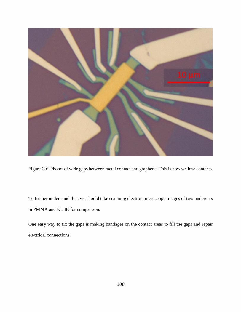
108
Figure C.6 Photos of wide gaps between metal contact and graphene. This is how we lose contacts.
To further understand this, we should take scanning electron microscope images of two undercuts
in PMMA and KL IR for comparison.
One easy way to fix the gaps is making bandages on the contact areas to fill the gaps and repair
electrical connections.

109
Figure C.7 Photo of metal bandages made to fill the gaps and repair the contacts.
Appendix D
Simulation by COMSOL Multiphysics
The simulation we use in our EMR project is based on the finite element method, which is a
numerical method subdividing a large system into smaller and simpler parts called finite elements.
These finite elements are modelled by the simple equations, which are then assembled into a larger
system of equations to model the entire problem.
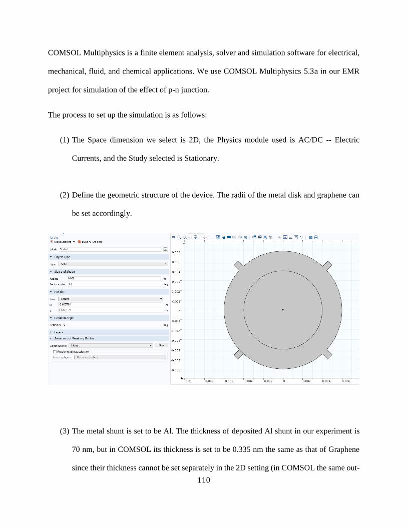
110
COMSOL Multiphysics is a finite element analysis, solver and simulation software for electrical,
mechanical, fluid, and chemical applications. We use COMSOL Multiphysics 5.3a in our EMR
project for simulation of the effect of p-n junction.
The process to set up the simulation is as follows:
(1) The Space dimension we select is 2D, the Physics module used is AC/DC -- Electric
Currents, and the Study selected is Stationary.
(2) Define the geometric structure of the device. The radii of the metal disk and graphene can
be set accordingly.
(3) The metal shunt is set to be Al. The thickness of deposited Al shunt in our experiment is
70 nm, but in COMSOL its thickness is set to be 0.335 nm the same as that of Graphene
since their thickness cannot be set separately in the 2D setting (in COMSOL the same out-

111
of-plane thickness has to be set for all domains). To proportionally compensate the
thickness change, I changed the conductivity of Al from 3.774e7 S/m to 788.597e7 S/m.
The calculation is simple, the conductivity 𝜎 can be expressed as the resistivity 𝜌 or as the
resistance 𝑅, the length l, the width 𝜔 and the thickness 𝑡:
𝜎 =1
𝜌=
𝑙
𝑅𝜔𝑡
𝜎t =𝑙
𝑅𝜔
Since we only change 𝜎 𝑎𝑛𝑑 t in the setting, 𝑅, l and 𝜔 should not change:
𝜎𝐴𝑙t𝐴𝑙 = 𝜎t𝐺
Since 𝜎𝐴𝑙 = 3.774𝑒7𝑆/𝑚, t𝐴𝑙 = 70𝑛𝑚, t𝐺 = 0.335𝑛𝑚,
We can get 𝜎 = 788.597𝑒7𝑆/𝑚. This is the adjusted conductivity of Al with the same
thickness of graphene.

112
(4) The outer ring is graphene, the electrical conductivity of which is represented by our
mathematical equations (4.3) to (4.6), which include the effect of doping and gate voltage.
(5) The top two probes are voltage probes, and the bottom left probe is current source with
I=100 nA. The bottom right probe is grounded.

113
(6) The 2D setting only has x axis and y axis and doesn’t not have z axis. So the 2D setting in
COMSOL doesn’t allow any physics vector in z direction, such as the electric field
perpendicular to the plane. But there is a way to encounter this issue: in the setting of
parametric sweep, we can set the range of the gate voltage we want to sweep with, and the
gate voltage is already included in the equation. The right picture below shows the meshed
device, which is ready for calculation.
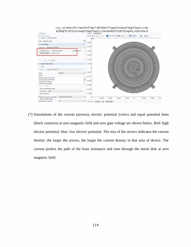
114
(7) Simulations of the current (arrows), electric potential (color) and equal potential lines
(black contours) at zero magnetic field and zero gate voltage are shown below. Red: high
electric potential, blue: low electric potential. The size of the arrows indicates the current
density: the larger the arrows, the larger the current density in that area of device. The
current prefers the path of the least resistance and runs through the metal disk at zero
magnetic field.

115
(8) The magnetic field can be set in the parametric sweep setting too. So the current in the
device at zero field and high field are respectively shown below. The current gets deflected
from the metal and run through the two sides of graphene at high field.
The simulation or calculation done by COMSOL provides the electric potentials at the two voltage
probes along with the corresponding gate voltages. The data can be exported to Excel to calculate

116
the voltages and resistances (since the current is set to a fixed value), which are used to plot the
voltage or resistance as a function of the gate voltage in Mathematica or Igor. The calculated
resistance is eventually compared with the experimental measured resistance, shown in Chapter 4.
![Suppression of intrinsic roughness in encapsulated graphene · tilt analysis in the transmission electron microscope (TEM) [2,20]. In contrast to scanning probe techniques, this method](https://static.fdocuments.net/doc/165x107/5f3ed37e48dd6e68c82ac328/suppression-of-intrinsic-roughness-in-encapsulated-graphene-tilt-analysis-in-the.jpg)