Extending FPGA Verification Through The PLI
14
1 Extending FPGA Verification Through The PLI Charles Howard Senior Research Engineer Southwest Research Institute San Antonio, Texas (210) 522-3419 [email protected]
-
Upload
lazzaro-murphy -
Category
Documents
-
view
40 -
download
0
description
Extending FPGA Verification Through The PLI. Charles Howard Senior Research Engineer Southwest Research Institute San Antonio, Texas (210) 522-3419 [email protected]. Background. Verilog is a hardware description language for digital logic design (FPGA/ASIC/PLD) Typical usage - PowerPoint PPT Presentation
Transcript of Extending FPGA Verification Through The PLI

1
Extending FPGA Verification Through The PLI
Charles HowardSenior Research Engineer
Southwest Research InstituteSan Antonio, Texas
(210) [email protected]
Howard MAPLD2005/1932
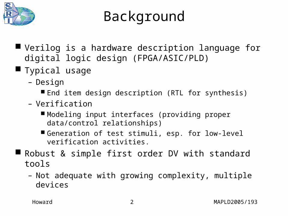
Background
Verilog is a hardware description language for digital logic design (FPGA/ASIC/PLD)
Typical usage– Design
End item design description (RTL for synthesis)
– Verification Modeling input interfaces (providing proper
data/control relationships) Generation of test stimuli, esp. for low-level
verification activities.
Robust & simple first order DV with standard tools– Not adequate with growing complexity, multiple
devices
Howard MAPLD2005/1933
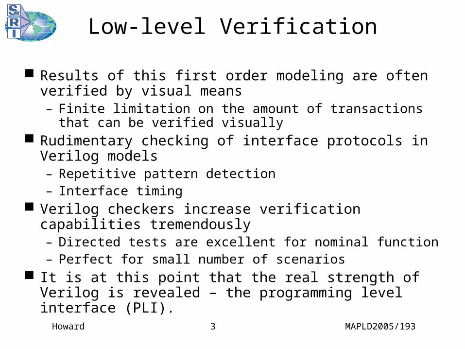
Low-level Verification
Results of this first order modeling are often verified by visual means – Finite limitation on the amount of transactions that
can be verified visually Rudimentary checking of interface protocols in
Verilog models– Repetitive pattern detection – Interface timing
Verilog checkers increase verification capabilities tremendously – Directed tests are excellent for nominal function– Perfect for small number of scenarios
It is at this point that the real strength of Verilog is revealed – the programming level interface (PLI).

Howard MAPLD2005/1934
The Verilog PLI
The Programming Language Interface is a procedural interface between Verilog simulation and other software programs– Verilog models can invoke external program during
simulation Accessibility to every attribute within the
simulation structure Capability to read and/or modify any value in the
simulation Flexibility to perform any simulation task
– Initializing memories at simulation start– Verifying end of simulation results.
Howard MAPLD2005/1935
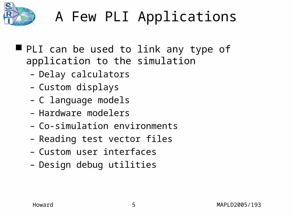
A Few PLI Applications
PLI can be used to link any type of application to the simulation– Delay calculators– Custom displays– C language models– Hardware modelers – Co-simulation environments– Reading test vector files– Custom user interfaces– Design debug utilities

Howard MAPLD2005/1936
PLI Implementations
C programs can be tied through the PLI to Verilog shell models
C programs then used to: – Dynamically generate test stimuli– Check design outputs– Scoreboard non-linear data flows – Incorporate random features
Layered approach – Sequences and scenarios
Random and directed
– Coverage
Howard MAPLD2005/1937
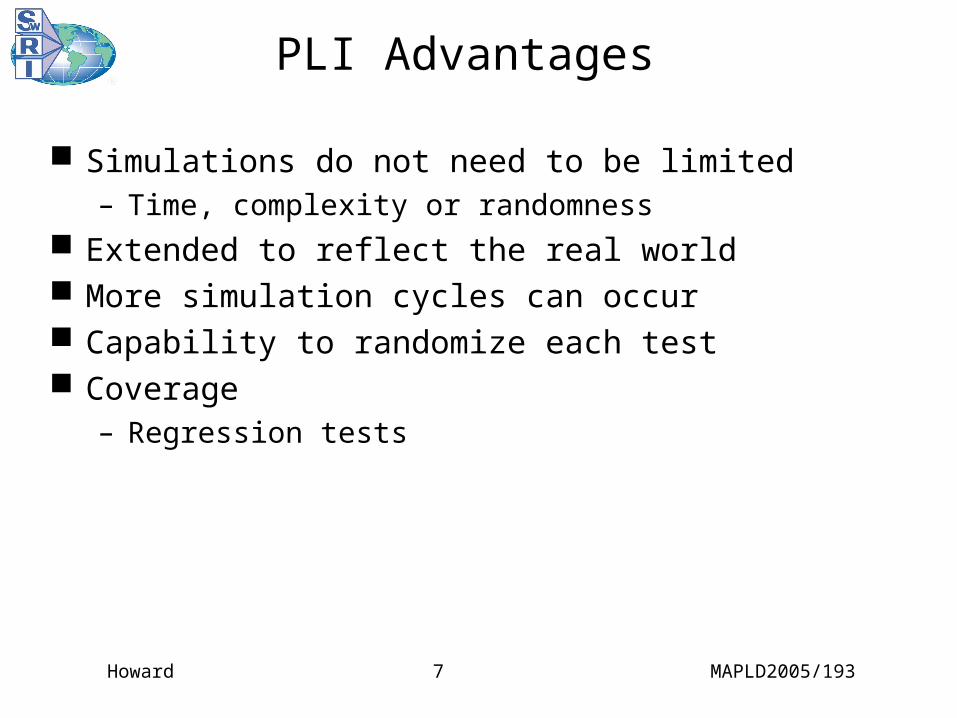
PLI Advantages
Simulations do not need to be limited– Time, complexity or randomness
Extended to reflect the real world More simulation cycles can occur Capability to randomize each test Coverage
– Regression tests

Howard MAPLD2005/1938
PLI Goal
In short, the PLI allows the designer to build a robust virtual test bench that allows the functional interaction of hardware and software to first be characterized without lab space.– Recent experiences (what I have learned in the
customer’s lab) Flow Control from multiple sources FSW access order

Howard MAPLD2005/1939
Randomization
An immense number of HW/SW interactions can be characterized for flaws
Using random and directed test techniques, functional verification of the logic design can be extended far beyond first order techniques.
Resulting design is much more robust and likely to function when moved into silicon.
Howard MAPLD2005/19310
Our approach
PLI extension of FPGA verification capabilities Development of several key bus functional models
and PLI routines Specific approaches and examples will be
presented.
Howard MAPLD2005/19311
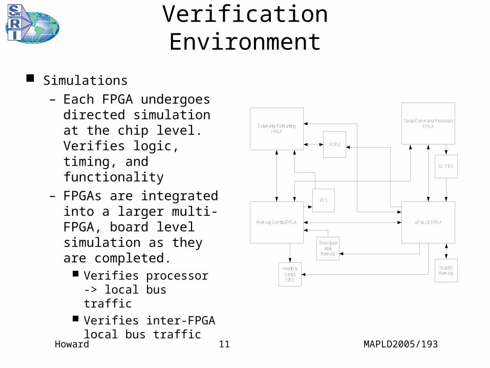
Verification Environment
Simulations– Each FPGA undergoes
directed simulation at the chip level. Verifies logic, timing, and functionality
– FPGAs are integrated into a larger multi-FPGA, board level simulation as they are completed.
Verifies processor -> local bus traffic
Verifies inter-FPGA local bus traffic
uP to LB FPGAMemory Control FPGA
Telemetry FormattingFPGA
Serial Command ProcessorFPGA
Downloadable
Memory
Health &StatusFIFO
VC1
VC0,2
SC FIFO
ScratchMemory
Howard MAPLD2005/19312
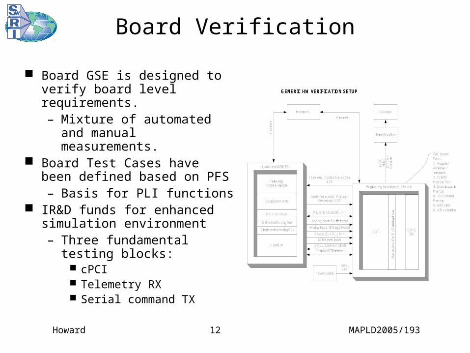
Board Verification
Board GSE is designed to verify board level requirements. – Mixture of automated and
manual measurements. Board Test Cases have been
defined based on PFS – Basis for PLI functions
IR&D funds for enhanced simulation environment – Three fundamental
testing blocks: cPCI Telemetry RX Serial command TX
Monitor PC
DUT
Digital I/O
Single ended Analog Out
MIL-STD-1553B
Break-Out Box
O-Scope
Board Level GSE PC
Engineering Development Chassis
LL
DC
HL
DC
(Bin
ary
)O
utp
uts
32 Bi-Level Inputs
16 GSE Bi-Level Outputs
Serial UARTInterface
Resets (3), VTC_LTCH
MIL-STD-1553B BC / RT
SBC Based
Tests:
1. RegisterAccesses /
Interrupts
2. Scratch
Memory Test3. Downloadable
Memory
4. 1553 Shared
Memory5. H&S FIFO
6. A/D Validation
Power Supply
+28V,+7V
Eth
ern
et
Ethernet
Analog Inputs 16 Single Ended
Ba
ckp
lan
e (
PW
R),
Sta
nd
ard
Bu
s
COTSSBC
Differential Analog Out Analog Inputs 8 Differential
Serial commands
Telemetry:Parse & decode
Serial commands: Primary /Secondary / GSE
Telemetry: Carrier, Sub-carrier,GSE
GENERIC HW VERIFICATION SETUP
Howard MAPLD2005/19313
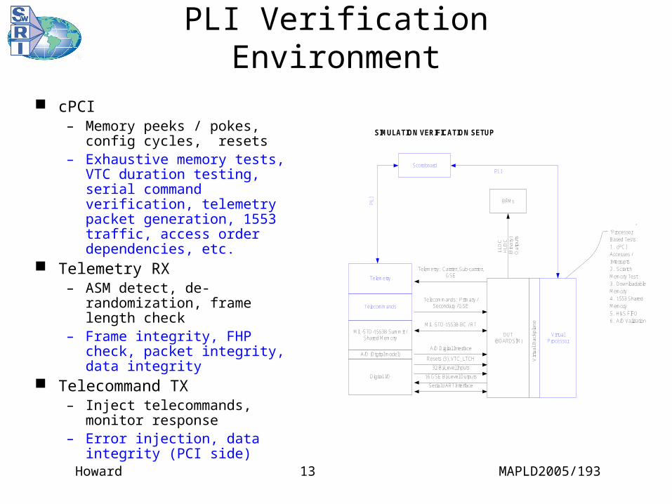
PLI Verification Environment
cPCI– Memory peeks / pokes,
config cycles, resets– Exhaustive memory tests,
VTC duration testing, serial command verification, telemetry packet generation, 1553 traffic, access order dependencies, etc.
Telemetry RX– ASM detect, de-
randomization, frame length check
– Frame integrity, FHP check, packet integrity, data integrity
Telecommand TX– Inject telecommands,
monitor response– Error injection, data integrity
(PCI side)
Scoreboard
DUT(BOARDSIM)
Digital I/O
MIL-STD-1553B Summit /Shared Memory
BFMs
LL
DC
HL
DC
(Bin
ary
) O
utp
uts
32 Bi-Level Inputs
16 GSE Bi-Level Outputs
Serial UARTInterface
Resets (3), VTC_LTCH
MIL-STD-1553B BC / RT
PL
I
PLI
A/D Digital Interface
Vir
tua
l B
ackp
lan
e
VirtualProcessor
A/D (Digital model)
Telecommands
Telemetry
Telecommands: Primary /Secondary / GSE
Telemetry: Carrier, Sub-carrier,GSE
SIMULATION VERIFICATION SETUP
“Processor”Based Tests:1. cPCIAccesses /Interrupts2. ScratchMemory Test3. DownloadableMemory4. 1553 SharedMemory5. H&S FIFO6. A/D Validation
Howard MAPLD2005/19314
Results
Simulation run length Coverage metrics
COME ON, NOW, REALLY… I’m still working on this, and trying to bring up hardware in the lab!!!