Energy-Efficient Spin-Transfer Torque RAM Cache Exploiting ...

EXPLOITING PROPERTIES OF CMP CACHE
TRAFFIC IN DESIGNING HYBRID
PACKET/CIRCUIT SWITCHED NOCS
by
Ahmed Abousamra
B.Sc., Alexandria University, Egypt, 2000
M.S., University of Pittsburgh, 2012
Submitted to the Graduate Faculty of
Computer Science Program,
The DIETRICH School of Arts and Sciences
in partial fulfillment
of the requirements for the degree of
Ph.D.
University of Pittsburgh
2013

UNIVERSITY OF PITTSBURGH
THE DIETRICH SCHOOL OF ARTS AND SCIENCES
This dissertation was presented
by
Ahmed Abousamra
It was defended on
July 15th, 2013
and approved by
Prof. Rami Melhem, Department of Computer Science
Prof. Alex Jones, Department of Electrical and Computer Engineering
Prof. Bruce Childers, Department of Computer Science
Prof. Sangyeun Cho, Department of Computer Science
Dissertation Director: Prof. Rami Melhem, Department of Computer Science
ii

EXPLOITING PROPERTIES OF CMP CACHE TRAFFIC IN DESIGNING
HYBRID PACKET/CIRCUIT SWITCHED NOCS
Ahmed Abousamra, PhD
University of Pittsburgh, 2013
Chip multiprocessors with few to tens of processing cores are already commercially available.
Increased scaling of technology is making it feasible to integrate even more cores on a single
chip. Providing the cores with fast access to data is vital to overall system performance.
When a core requires access to a piece of data, the core’s private cache memory is searched
first. If a miss occurs, the data is looked up in the next level(s) of the memory hierarchy,
where often one or more levels of cache are shared between two or more cores. Communi-
cation between the cores and the slices of the on-chip shared cache is carried through the
network-on-chip(NoC). Interestingly, the cache and NoC mutually affect the operation of
each other; communication over the NoC affects the access latency of cache data, while the
cache organization generates the coherence and data messages, thus affecting the communi-
cation patterns and latency over the NoC.
This thesis considers hybrid packet/circuit switched NoCs, i.e., packet switched NoCs
enhanced with the ability to configure circuits. The communication and performance benefit
that come from using circuits is predicated on amortizing the time cost incurred for config-
uring the circuits. To address this challenge, NoC designs are proposed that take advantage
of properties of the cache traffic, namely temporal locality and predictability, to amortize or
hide the circuit configuration time cost.
First, a coarse-grained circuit configuration policy is proposed that exploits the temporal
locality in the cache traffic to periodically configure circuits for the heavily communicating
nodes. This allows the design of a locality-aware cache that promotes temporal commu-
iii

nication locality through data placement, while designing suitable data replacement and
migration policies.
Next, a fine-grained configuration policy, called Deja Vu switching, is proposed for lever-
aging predictability of data messages by initiating a circuit configuration as soon as a cache
hit is detected and before the data becomes available. Its benefit is demonstrated for saving
interconnect energy in multi-plane NoCs.
Finally, a more proactive configuration policy is proposed for fast caches, where circuit
reservations are initiated by request messages, which can greatly improve communication
latency and system performance.
Keywords: Multi-core/single-chip multiprocessors, CMP, NoC, packet switching, circuit
switching, Locality-Aware Cache.
iv

TABLE OF CONTENTS
1.0 INTRODUCTION . . . . . . . . . . . . . . . . . . . . . . . . . . . . . . . . . 1
1.1 Goal . . . . . . . . . . . . . . . . . . . . . . . . . . . . . . . . . . . . . . . . 1
1.2 Overview of the Proposed Approaches . . . . . . . . . . . . . . . . . . . . . 2
2.0 BACKGROUND AND RELATED WORK . . . . . . . . . . . . . . . . . 6
2.1 Chip Multiprocessor . . . . . . . . . . . . . . . . . . . . . . . . . . . . . . . 6
2.2 Network-on-Chip . . . . . . . . . . . . . . . . . . . . . . . . . . . . . . . . . 7
2.2.1 Packet Switching . . . . . . . . . . . . . . . . . . . . . . . . . . . . . . 7
2.2.2 Hybrid Packet/Circuit Switching . . . . . . . . . . . . . . . . . . . . . 9
2.2.3 Circuit Configuration with an On-Demand Policy . . . . . . . . . . . 9
2.3 Cache Design . . . . . . . . . . . . . . . . . . . . . . . . . . . . . . . . . . . 10
2.4 Related Work . . . . . . . . . . . . . . . . . . . . . . . . . . . . . . . . . . . 11
2.4.1 NoC: Speeding Communication With Reduced Hop Count . . . . . . 11
2.4.2 NoC: Speeding Communication With Reduced Hop Latency . . . . . . 13
2.4.3 NoC: Reducing Communication Power . . . . . . . . . . . . . . . . . . 14
2.4.4 Cache Design . . . . . . . . . . . . . . . . . . . . . . . . . . . . . . . . 15
3.0 COARSE-GRAIN CIRCUIT CONFIGURATION AND PINNING . . 17
3.1 Hybrid Packet/Circuit Switched Interconnect with Pinned Circuit Configu-
ration . . . . . . . . . . . . . . . . . . . . . . . . . . . . . . . . . . . . . . . 18
3.1.1 Circuit Configuration Algorithms . . . . . . . . . . . . . . . . . . . . 19
3.1.1.1 A Centralized Algorithm . . . . . . . . . . . . . . . . . . . . . 20
3.1.1.2 A Distributed Algorithm . . . . . . . . . . . . . . . . . . . . . 20
3.2 Implementation Issues . . . . . . . . . . . . . . . . . . . . . . . . . . . . . . 22
v

3.2.1 Router Design . . . . . . . . . . . . . . . . . . . . . . . . . . . . . . . 22
3.2.2 Delayed Circuit Reconfiguration at a Router . . . . . . . . . . . . . . 23
3.2.3 CFC bit versus lookahead signal . . . . . . . . . . . . . . . . . . . . . 23
3.3 Routing on Partial Circuits . . . . . . . . . . . . . . . . . . . . . . . . . . . 23
3.4 Evaluation Methodology . . . . . . . . . . . . . . . . . . . . . . . . . . . . . 25
3.5 Evaluation Results . . . . . . . . . . . . . . . . . . . . . . . . . . . . . . . . 28
3.5.1 Average Flit Latency . . . . . . . . . . . . . . . . . . . . . . . . . . . 28
3.5.2 Execution Time . . . . . . . . . . . . . . . . . . . . . . . . . . . . . . 29
3.5.3 Circuits Utilization . . . . . . . . . . . . . . . . . . . . . . . . . . . . 31
3.6 Conclusion . . . . . . . . . . . . . . . . . . . . . . . . . . . . . . . . . . . . 31
4.0 LOCALITY-AWARE CACHE DESIGN TO MAXIMIZE THE BEN-
EFITS OF COARSE GRAINED CIRCUIT CONFIGURATION . . . . 33
4.1 Motivation . . . . . . . . . . . . . . . . . . . . . . . . . . . . . . . . . . . . 34
4.2 Unique Private: A Locality-Aware Cache . . . . . . . . . . . . . . . . . . . . 35
4.2.1 Data Placement and Lookup . . . . . . . . . . . . . . . . . . . . . . . 36
4.2.2 Data Migration . . . . . . . . . . . . . . . . . . . . . . . . . . . . . . 39
4.2.3 Data Replacement Policy . . . . . . . . . . . . . . . . . . . . . . . . . 40
4.3 Evaluation . . . . . . . . . . . . . . . . . . . . . . . . . . . . . . . . . . . . 41
4.3.1 Background: The Circuit Switched Coherence Co-designed Scheme . . 41
4.3.2 Evaluation Environment . . . . . . . . . . . . . . . . . . . . . . . . . 43
4.3.3 Evaluation Results . . . . . . . . . . . . . . . . . . . . . . . . . . . . . 45
4.4 Conclusion . . . . . . . . . . . . . . . . . . . . . . . . . . . . . . . . . . . . 51
5.0 DEJA VU SWITCHING: FINE-GRAINED CIRCUIT CONFIGURA-
TION FOR MULTIPLANE NOCS . . . . . . . . . . . . . . . . . . . . . . 53
5.1 Motivation . . . . . . . . . . . . . . . . . . . . . . . . . . . . . . . . . . . . 54
5.2 Split-plane Interconnect Design . . . . . . . . . . . . . . . . . . . . . . . . . 55
5.3 Deja Vu Switching For Multi-Plane Interconnects . . . . . . . . . . . . . . . 57
5.3.1 Connection Reservation and Realization with Head of Queues Duo
Matching (HQDM) . . . . . . . . . . . . . . . . . . . . . . . . . . . . 59
5.4 Analysis of acceptable data plane slowdown . . . . . . . . . . . . . . . . . . 61
vi

5.4.1 R-packet arrives at a router before the data packet . . . . . . . . . . . 62
5.4.2 Critical words are not delayed . . . . . . . . . . . . . . . . . . . . . . 63
5.4.3 Delayed cache hits are not overly delayed . . . . . . . . . . . . . . . . 63
5.4.4 Computing the slow-down factor . . . . . . . . . . . . . . . . . . . . . 64
5.5 Evaluation . . . . . . . . . . . . . . . . . . . . . . . . . . . . . . . . . . . . 65
5.5.1 Evaluation with synthetic traces . . . . . . . . . . . . . . . . . . . . . 65
5.5.2 Evaluation with benchmarks . . . . . . . . . . . . . . . . . . . . . . . 69
5.6 Conclusion . . . . . . . . . . . . . . . . . . . . . . . . . . . . . . . . . . . . 71
6.0 RED CARPET ROUTING: A FINE-GRAINED PROACTIVE CIR-
CUIT ALLOCATION IN MULTIPLANE NOCS . . . . . . . . . . . . . . 72
6.1 Proactive Circuit Allocation . . . . . . . . . . . . . . . . . . . . . . . . . . . 73
6.1.1 Network Architecture . . . . . . . . . . . . . . . . . . . . . . . . . . . 73
6.1.2 Reserving Circuits . . . . . . . . . . . . . . . . . . . . . . . . . . . . . 74
6.1.3 Realizing Reserved Circuits . . . . . . . . . . . . . . . . . . . . . . . . 76
6.2 Ensuring Correct Routing on Reserved Circuits . . . . . . . . . . . . . . . . 78
6.2.1 Detecting and Handling a Reservation Conflict While Reserving a New
Circuit . . . . . . . . . . . . . . . . . . . . . . . . . . . . . . . . . . . 81
6.2.2 Detecting a Reservation Conflict While a Message is Traversing a Circuit 83
6.3 Avoiding Deadlock . . . . . . . . . . . . . . . . . . . . . . . . . . . . . . . . 85
6.4 Improving Quality of Estimation . . . . . . . . . . . . . . . . . . . . . . . . 86
6.5 Handling Cases When Circuit Pre-Allocation is Not Possible . . . . . . . . . 87
6.6 Implementation Issues . . . . . . . . . . . . . . . . . . . . . . . . . . . . . . 89
6.6.1 EUC Representation . . . . . . . . . . . . . . . . . . . . . . . . . . . . 90
6.6.2 Breaking Ties . . . . . . . . . . . . . . . . . . . . . . . . . . . . . . . 91
6.7 Discussion: using Red Carpet Routing for saving power . . . . . . . . . . . 92
6.8 Evaluation of Proactively Allocated Circuits . . . . . . . . . . . . . . . . . . 92
6.8.1 Performance Evaluation . . . . . . . . . . . . . . . . . . . . . . . . . . 94
6.8.1.1 Round-Trip Time Estimation . . . . . . . . . . . . . . . . . . 96
6.8.1.2 Forward Circuits as a Fallback . . . . . . . . . . . . . . . . . . 96
6.9 Conclusion . . . . . . . . . . . . . . . . . . . . . . . . . . . . . . . . . . . . 98
vii

7.0 SUMMARY AND CONCLUSION OF THE THESIS . . . . . . . . . . . 100
7.1 Future Work . . . . . . . . . . . . . . . . . . . . . . . . . . . . . . . . . . . 103
BIBLIOGRAPHY . . . . . . . . . . . . . . . . . . . . . . . . . . . . . . . . . . . . 106
viii

LIST OF TABLES
1 Benchmarks Description . . . . . . . . . . . . . . . . . . . . . . . . . . . . . . 27
2 Benchmarks Description . . . . . . . . . . . . . . . . . . . . . . . . . . . . . . 45
3 Pseudo-code summarizing the routing actions performed on the control and
data planes as part of Deja Vu switching. . . . . . . . . . . . . . . . . . . . . 60
4 Specifications of virtual channels . . . . . . . . . . . . . . . . . . . . . . . . . 64
5 Voltage and frequency of the evaluated data planes. . . . . . . . . . . . . . . 66
ix
LIST OF FIGURES
1 Network switching: packet, circuit, and hybrid packet/circuit switched NoCs. 2
2 Diagram of a tiled CMP having 9 cores. The tiles are laid out in a 2D mesh.
Each tile has a processing core, a private I/D L1 cache, a slice of the L2
cache, a slice of a distributed directory for maintaining cache coherency, and a
network interface (NI). Each NI is connected to the router(s) of the interconnect
plane(s) at the tile. . . . . . . . . . . . . . . . . . . . . . . . . . . . . . . . . 7
3 Diagram of a Packet Switched Router . . . . . . . . . . . . . . . . . . . . . . 8
4 Microarchitecture of hybrid packet/circuit switched router. . . . . . . . . . . 10
5 % of traffic traveling on complete circuits from source to destination
. . . . . . . . . . . . . . . . . . . . . . . . . . . . . . . . . . . . . . . . . . . 17
6 Average number of cycles between sending two consecutive packets from the
same source to the same destination . . . . . . . . . . . . . . . . . . . . . . . 17
7 Microarchitecture of hybrid packet/circuit switched router. . . . . . . . . . . 22
8 SNUCA L2 (1MB) - Normalized average flit latency . . . . . . . . . . . . . . 27
9 Private L2 (1MB) - Normalized average flit latency . . . . . . . . . . . . . . . 27
10 SNUCA L2 (256KB) - Normalized average flit latency . . . . . . . . . . . . . 28
11 Private L2 (256KB) - Normalized average flit latency . . . . . . . . . . . . . . 28
12 SNUCA L2 (1MB) - Normalized execution time . . . . . . . . . . . . . . . . . 28
13 Private L2 (1MB) - Normalized execution time . . . . . . . . . . . . . . . . . 28
14 SNUCA L2 (256KB) - Normalized execution time . . . . . . . . . . . . . . . 29
15 Private L2 (256KB) - Normalized execution time . . . . . . . . . . . . . . . . 29
16 SNUCA L2 (1MB) - % Flits using complete circuits . . . . . . . . . . . . . . 29
x

17 Private L2 (1MB) -% Flits using complete circuits . . . . . . . . . . . . . . . 29
18 SNUCA L2 (256KB) - % Flits using complete circuits . . . . . . . . . . . . . 30
19 Private L2 (256KB) -% Flits using complete circuits . . . . . . . . . . . . . . 30
20 SNUCA L2 (1MB) - % Flits using partial circuits . . . . . . . . . . . . . . . . 30
21 Private L2 (1MB) - % Flits using partial circuits . . . . . . . . . . . . . . . . 30
22 SNUCA L2 (256KB) - % Flits using partial circuits . . . . . . . . . . . . . . 31
23 Private L2 (256KB) - % Flits using partial circuits . . . . . . . . . . . . . . . 31
24 Performance speedup of each cache with the hybrid packet/circuit switched
and on-demand circuit establishment NoC, relative to the same cache with the
packet switched NoC . . . . . . . . . . . . . . . . . . . . . . . . . . . . . . . 34
25 Example of core Pi accessing cache block bj in L2 . . . . . . . . . . . . . . . . 37
26 Performance speedup relative to the system with O2000P cache + CSOD NoC
. . . . . . . . . . . . . . . . . . . . . . . . . . . . . . . . . . . . . . . . . . . 46
27 Effect of Migration and LDC - Performance speedup relative to the system
with O2000P cache + CSP NoC . . . . . . . . . . . . . . . . . . . . . . . . . 46
28 Comparing Migration Policies: Performance speedup relative to the system
with O2000P cache + CSP NoC . . . . . . . . . . . . . . . . . . . . . . . . . 47
29 Comparing Migration Policies: Percentage of the traffic volume used for mi-
gration messages . . . . . . . . . . . . . . . . . . . . . . . . . . . . . . . . . . 47
30 Effect on NoC: Traffic volume normalized to the system with O2000P cache +
CSP NoC . . . . . . . . . . . . . . . . . . . . . . . . . . . . . . . . . . . . . . 49
31 Effect on NoC: Average number of most important circuits created
. . . . . . . . . . . . . . . . . . . . . . . . . . . . . . . . . . . . . . . . . . . 49
32 Effect on NoC - Average flit latency normalized to the system with O2000P +
CSP NoC . . . . . . . . . . . . . . . . . . . . . . . . . . . . . . . . . . . . . . 50
33 Performance speedup of systems using SBLRU relative to corresponding sys-
tems using LRU . . . . . . . . . . . . . . . . . . . . . . . . . . . . . . . . . . 50
34 Performance speedup (for 64 cores) relative to the system with O2000P cache
+ CSP NoC . . . . . . . . . . . . . . . . . . . . . . . . . . . . . . . . . . . . 50
35 Percentage of delayed hits out of all L1 misses using the baseline NoC. . . . . 55
xi

36 Diagrams of the control and data plane’s routers (not to scale). . . . . . . . . 57
37 Synthetic traffic - Communication latency on a 64-core CMP. . . . . . . . . . 67
38 Synthetic traffic - Normalized execution completion time and NoC energy con-
sumption on a 64-core CMP. . . . . . . . . . . . . . . . . . . . . . . . . . . . 68
39 16 core CMP - Normalized execution time and NoC energy consumption. . . 68
40 64 core CMP - Normalized execution time and NoC energy consumption. . . 69
41 Comparing performance on a 16-core CMP with split-plane NoCs, with and
without Deja Vu switching (Y-axis starts at 0.9) . . . . . . . . . . . . . . . . 70
42 Example showing that realizing reverse circuits in a FCFS order can result in
poor utilization of the NoC resources (See Section 6.1.2) . . . . . . . . . . . . 75
43 Checking if the new reverse reservation has the earliest EUC among existing
reservations. . . . . . . . . . . . . . . . . . . . . . . . . . . . . . . . . . . . . 77
44 Example: Realizing circuit reservations in ascending order of their EUCs. The
west-east connection is realized before the south-east connection. . . . . . . . 77
45 Updating the pmin pointer by finding the next reservation with the earliest EUC. 78
46 The solid line represents the shared sub-path between circuits C1 and C2. C1
is scheduled before C2, thus m1 crosses the shared sub-path before m2 . . . . 79
47 Circuit C1 is scheduled before C2, but the right part of C1 in the dotted line
is not yet reserved. Message m2 starts traversing the shared sub-path between
C1 and C2 before C1 is completely reserved on it. If no corrective measure is
taken, m2 would wrongly travel on C1 instead of remaining on C2. . . . . . . 79
48 Detecting a reservation conflict: In the example request Req1 is reserving cir-
cuit C1 and message m2 is traveling on circuit C2. (a) The last successful
reservation of C1 at router Rj+1, and m2 successfully traverses Rj while cor-
rectly traveling on C2. (b) Reservation conflict is detected upon attempting to
reserve C1 at router Rj, and a corrective action is required to avoid misrouting
m2 on C1. . . . . . . . . . . . . . . . . . . . . . . . . . . . . . . . . . . . . . . 82
49 A circular dependency that causes deadlock. The events are numbered to help
explain how the deadlock develops. . . . . . . . . . . . . . . . . . . . . . . . . 84
xii

50 Diagrams of the control and data plane’s routers with support for both forward
and reverse reservations. . . . . . . . . . . . . . . . . . . . . . . . . . . . . . . 88
51 Tracked time intervals. All reservations falling in I−2 are maintained in as-
cending order in the reservation buffers. . . . . . . . . . . . . . . . . . . . . . 90
52 Average L2 hit latency normalized to the purely packet switched system (the
Y-axis starts at 0.7).
. . . . . . . . . . . . . . . . . . . . . . . . . . . . . . . . . . . . . . . . . . . 94
53 Identification of communication sensitive benchmarks by examining the exe-
cution time speedup using the Ideal NoC (the Y-axis starts at 1.0) . . . . . . 94
54 Execution time speedup of CMPs with the DV and RCR NoCs (the Y-axis
starts at 1.0). Communication sensitive benchmarks are displayed on the right
of the chart. . . . . . . . . . . . . . . . . . . . . . . . . . . . . . . . . . . . . 95
55 Percentage achieved of the performance of the CMP with the ideal NoC.
. . . . . . . . . . . . . . . . . . . . . . . . . . . . . . . . . . . . . . . . . . . 95
56 Comparing the execution time speedup with different round-trip times estima-
tion methods. . . . . . . . . . . . . . . . . . . . . . . . . . . . . . . . . . . . 96
57 Percentage of released circuits relative to the number of requests performing
circuit reservations. . . . . . . . . . . . . . . . . . . . . . . . . . . . . . . . . 96
58 Percentage increase of flits sent over the RCR NoC compared to the DV NoC. 97
59 Normalized energy of the RCR NoC to the DV NoC. . . . . . . . . . . . . . . 98
xiii

LIST OF EQUATIONS
5.1 Equation (5.1) . . . . . . . . . . . . . . . . . . . . . . . . . . . . . . . . . . . 62
5.2 Equation (5.2) . . . . . . . . . . . . . . . . . . . . . . . . . . . . . . . . . . . 63
5.3 Equation (5.3) . . . . . . . . . . . . . . . . . . . . . . . . . . . . . . . . . . . 63
xiv
1.0 INTRODUCTION
Chip multiprocessors (CMPs) have processing cores with one or more levels of private caches
and often a shared last level cache. Examples include Intel’s Xeon processor [83] and AMD’s
Opteron processor [27]. One of the primary benefits of CMPs is having fast on-chip com-
munication, which makes them very suitable for running parallel workloads. The threads
of parallel workloads often share data, therefore causing multiple copies of the same data
to simultaneously exist in the private caches of different cores. The NoC allows the com-
munication necessary for exchanging data and ensuring data coherency; thus, both fast-
communication and efficient cache-design are critical to system performance.
1.1 GOAL
Generally, network traffic is either packet switched (PS) or circuit switched (CS). A packet
switched message is examined at each router of the path to make the necessary routing
decisions, such as which router output port and possibly which virtual channel the message
should use. A circuit switched message, on the other hand, does not suffer the overhead
of routing decisions because the circuit is either implemented as a direct point-to-point
connection between the sender and receiver, or if there are routers along the path, the routers
are pre-configured to send the incoming messages through the correct output ports without
incurring routing delays. This thesis considers packet switched NoCs enhanced with the
ability to configure circuits; i.e. hybrid packet/circuit switched NoCs. Circuits are realized
through the latter circuit implementation, in which routers are pre-configured to correctly
route the circuit switched messages.
1

A hybrid NoC may be composed of one or more planes. As illustrated in Fig. 1, a plane
in a hybrid NoC may support either: mixed packet and circuit switching (Unified hybrid
packet/circuit switching), or supports only one of packet or circuit switching (Segregated
hybrid packet/circuit switching).
In an ideal setting, circuits would simultaneously exist between every pair of communi-
cating nodes. However, this requires a huge amount of wiring which is not practical given
the limited chip area. Therefore, only a subset of all the circuits between communicating
nodes can be simultaneously established at any point in time. Further, there is a latency
cost for establishing a circuit, making circuits effective only if the cost can be amortized, for
example, through enough reuse. Given these limitations, this thesis proposes NoC
designs that exploit properties of the cache traffic for better configuring and
utilizing circuits to achieve performance and/or power gains.
Hybrid Packet / Circuit
Switching
Unified Hybrid PS/CS A plane supports both
packet and circuit switching
Segregated Hybrid PS/CS A plane supports either
packet or circuit switching
Network Switching
Packet Switching
Circuit Switching
Figure 1: Network switching: packet, circuit, and hybrid packet/circuit switched NoCs.
1.2 OVERVIEW OF THE PROPOSED APPROACHES
The thesis proposes two approaches for better utilizing the hybrid NoCs. The first is a coarse-
grained approach which exploits temporal locality of the cache traffic to increase utilization
of circuits and improve CMP performance (Chapter 3). In particular, since there is a latency
cost for establishing circuits, instead of establishing a circuit on-demand for every message
– an approach that suffers from potential thrashing of conflicting circuit paths and possibly
2

poor utilization of circuits – it is proposed to periodically identify the heavily communicating
nodes and configure circuits for them. The stability of established circuits until the next re-
configuration increases their re-use, and in addition allows speeding-up communication with
destinations not explicitly connected by circuits through routing on parts of established
ones. To further benefit from such a NoC, a locality-aware cache organization that promotes
communication locality is proposed (Chapter 4). With careful data placement, network
traffic can be reduced and communication locality can be increased. Moreover, the proposed
locality-aware cache includes suitable locality-aware data migration and data replacement
policies.
Considering the flow of messages resulting from cache transactions, the data request
messages in an efficient cache design should mostly hit in the on-chip cache resulting in data
reply messages to be sent soon after the requests are received; hence, making reply data
messages predictable for the most part. This predictability can be leveraged to pre-configure
circuits for the data messages; thus hiding part or all of the configuration time cost. This
thesis suggests two fine-grained approaches to circuits configuration that establish circuits
on a per-message basis while avoiding circuit thrashing.
The first approach is Deja Vu switching, a simple algorithm that initiates circuit config-
uration for a data message once it is confirmed that the corresponding cache request hits in
the cache (Chapter 5). The lead time between detecting a cache hit and reading and sending
the requested cache line allows hiding part or all of the circuit configuration time. Moreover,
since traveling on circuits is faster than packet switching, it is proposed to save power by
operating the circuits at a lower voltage/frequency than the packet switched traffic. Specifi-
cally, power can be saved if instead of having a single interconnect plane, the NoC is split into
two planes: a plane dedicated to the cache requests and control messages; and a slower, more
power efficient plane dedicated to the mostly predictable data messages. However, this split
can be beneficial for saving energy only if system performance is not significantly degraded
by the slower plane. Thus, the criticality of data messages is considered and an analysis of
the constraints that govern how slow the power-efficient plane can operate without hurting
system performance is developed.
The second approach, Red Carpet Routing, is proposed for improving the performance
3

of CMPs with fast on-chip caches (Chapter 6). With a fast enough cache, the time between
detecting a cache hit and reading the cache line may not be long enough for Deja Vu switch-
ing to be effective in hiding the time overhead of circuit configuration. Red Carpet Routing
aims to hide this time overhead by using request messages to reserve the circuits for their
anticipated reply messages. Reserving circuits by requests requires time-based reservations
to avoid holding NoC resources unnecessarily idle which under-utilizes the NoC. However,
variability in network traffic conditions and request processing times make it impossible to
use accurate time-based reservations. To solve this problem, approximate time-based reser-
vations are proposed, where requesting nodes estimate the time length of the round-trip from
the time when a request is sent until its reply is received, and these estimates are used for
ordering the realization of the reserved circuits.
To summarize, this thesis advocates that: “The overhead of circuit switching
is reduced with exploring knowledge of the system” and provides the following
contributions:
1. Leveraging communication locality in cache traffic to design a pinning (coarse-
grained) circuit configuration policy for speeding-up communication and
performance.
2. The introduction of a locality-aware cache organization that promotes com-
munication locality and maximizes the benefit from the pinning circuit con-
figuration policy.
3. Leveraging predictability of data messages in the cache traffic to design two
on-demand (fine-grained) circuit configuration policies for:
a. Reducing power consumption without sacrificing performance ( Deja Vu
switching) for CMP with relatively slow caches.
b. Improving performance and potentially power consumption of CMPs
with fast caches ( Red Carpet Routing).
The thesis is organized as follows. Related work and necessary background are described
in Chapter 2. Chapters 3 and 4 present the proposed pinning circuit configuration policy
4

for the NoC, and the locality-aware cache design, respectively. The proposed fine-grained
circuit configuration policies, Deja Vu switching and Red Carpet Routing, are presented in
Chapters 5 and 6. Finally, Chapter 7 presents a summary of the contributions, and how
they may be integrated in the CMP design, as well as future work.
5

2.0 BACKGROUND AND RELATED WORK
This chapter presents an overview of the tiled CMP architecture, along with a description
of packet switching, an overview of hybrid packet/circuit switched interconnects, and cache
organizations. Afterwards, related work is presented in the areas of improving the perfor-
mance of network-on-chip and its power consumption, as well as related work in the area of
efficient cache design.
2.1 CHIP MULTIPROCESSOR
The thesis considers a homogeneous chip multiprocessor architecture, i.e., all processing cores
are identical. More specifically, a tiled CMP architecture is assumed, where tiles are laid in
a 2D mesh, as in Fig. 2. Each tile consists of a processing core, private L1 cache (instruction
and data), an L2 bank, a directory to maintain coherence, and a network interface (NI).
The NI is the interface point between the tile and on-chip interconnect. It is responsible for
sending and receiving packets. In case there are multiple interconnect planes, the NI decides
on which plane to send each packet.
6

Core + L1 I/D Cache
L2 Cache NI
Directory
Core + L1 I/D Cache
L2 Cache NI
Directory
Core + L1 I/D Cache
L2 Cache NI
Directory
Core + L1 I/D Cache
L2 Cache NI
Directory
Core + L1 I/D Cache
L2 Cache NI
Directory
Core + L1 I/D Cache
L2 Cache NI
Directory
Core + L1 I/D Cache
L2 Cache NI
Directory
Core + L1 I/D Cache
L2 Cache NI
Directory
Core + L1 I/D Cache
L2 Cache NI
Directory
Figure 2: Diagram of a tiled CMP having 9 cores. The tiles are laid out in a 2D mesh. Each tilehas a processing core, a private I/D L1 cache, a slice of the L2 cache, a slice of a distributed
directory for maintaining cache coherency, and a network interface (NI). Each NI is connected tothe router(s) of the interconnect plane(s) at the tile.
2.2 NETWORK-ON-CHIP
2.2.1 Packet Switching
In packet switching packets travel to their destinations on interconnect links. After crossing
a link, a packet is received in an interconnect router, which examines the packet and decides
the next link the packet should be sent on. I.e., routers – as the name implies – implement
the logic for forwarding packets to their destinations. The different parts of this logic, which
are described below, are most often implemented as stages of a pipeline that is referred to
as the router pipeline.
Fig. 3 shows a diagram of a typical packet switched router. When the head flit of a packet
arrives at an input port of a router it is first decoded and buffered in the port’s input virtual
channel (VC) buffer during the buffer write (BW) stage of the router pipeline. Second, it
goes through the route computation (RC) stage during which routing logic computes the
output port for the packet. Next, the head flit arbitrates for an output virtual channel (VC)
in the virtual channel allocation (VA) stage. After arbitration succeeds and an output VC
7

VC1
VC2
VCn
…..
Input Buffers
VC1
VC2
VCn
…..
Input Buffers
Crossbar Switch
Route Computation
VC Allocator
Switch Allocator
Input 0
Input 4
. . . . . .
Output 0
Output 4
. . . . . .
Figure 3: Diagram of a Packet Switched Router
is allocated, the head flit competes for the switch input and output ports during the switch
allocation (SA) stage. Finally, the head flit proceeds to traverse the crossbar in the switch
traversal (ST) stage, followed by traversing the link in the link traversal (LT) stage. Body
and tail flits of the packet skip the RC and VA stages since they follow the head flit.
Several techniques can be applied to shorten the critical path through the router stages.
Lookahead routing, where route computation occurs in the BW stage, removes RC from
the router’s critical path. Aggressive speculation [71, 76] allows VA and SA stages to occur
simultaneously, where a head flit is allowed to enter SA stage assuming it will succeed in
allocating an output VC in the VA stage, but is not allowed to enter ST stage if it fails in
allocating an output VC, at which case the head flit will have to go through the VA and SA
stages again. Switch and link traversal can be performed together in one stage. Note that
further reduction of the router critical path to only one stage is possible under low loads
through aggressive speculation and bypassing [57].
8

2.2.2 Hybrid Packet/Circuit Switching
Hybrid packet/circuit switched interconnects support both packet switched (PS) and circuit
switched (CS) traffic. Packet switching is described above (Section 2.2.1). Circuit switching,
on the other hand, works by configuring a circuit from a source tile, S, to a destination tile,
D. A circuit is configured by specifying at each intermediate router which input port should
be connected to which output port during the SA stage. For unified hybrid packet/circuit
switching, where both packet and circuit switching are supported on the same plane (for
example, [33]), an extra bit, called circuit field check (CFC) may be added to each flit to
indicate whether the flit is circuit or packet switched. The CFC bit is checked when the
flit enters the router. If the CFC bit is set, the flit is allowed to bypass directly to the
switch traversal stage, otherwise it is buffered in the appropriate virtual channel buffer and
routed as packet switched. CS flits have higher priority than PS flits. The switch allocator
receives signals from the input ports indicating the presence or absence of incoming CS flits,
and accordingly determines which input ports can send PS flits. Fig. 4 shows a diagram
of a potential router supporting hybrid packet/circuit switching. It differs from the packet
switching router in Fig. 3 in that there is added logic for configuring circuits (as described in
the next section) and an added virtual channel, V CCS, for buffering circuit switched packets
if they cannot continue traveling on a circuit – for example, if a circuit is reconfigured or
removed when the packet is in flight; more details will be provided in Chapter 3.
2.2.3 Circuit Configuration with an On-Demand Policy
When a circuit is needed, a circuit configuration message must be sent first to configure the
circuit. A configuration message is usually small and travels packet switched configuring
the routers on the circuit path. Configuration messages may be sent on a dedicated setup
interconnect plane, which is the approach taken in [33], and described next:
The NoC may be comprised of one or more interconnect planes. To send a packet, pi,
from tile, S, to tile, D, either pi is sent on an already established circuit from S to D on
one of the interconnect planes, or if there is no such circuit, one of the interconnect planes is
chosen to establish the circuit. S sends a circuit setup request on the setup plane specifying
9

VC1
VC2
VCn
VCCS
…..
Input Buffers
VC1
VC2
VCn
VCCS
…..
Input Buffers Crossbar Switch
Route Computation
VC Allocator
Switch Allocator
Circ
uit s
Co
nfig
urat
ion
Input 0
Input 4
. . . . . .
Output 0
Output 4
. . . . . .
Figure 4: Microarchitecture of hybrid packet/circuit switched router.
the destination D and the chosen interconnect plane on which to establish the circuit. S does
not wait for the circuit to be established, but rather sends the packet immediately behind
the circuit setup request. When S wishes to subsequently send another packet, pj, to D, it
can be sent on the established circuit if it is still in place, i.e., if the circuit is not torn down
during the time between the two packets pi and pj are sent.
When an existing circuit, Cold, from S to D is torn down at an intermediate router, Rk,
to allow a new conflicting circuit, Cnew, to be established, Rk asserts a reconfiguration signal
at the input port, ipj, of Cold so that an incoming CS packet at ipj is buffered and routed
as packet switched (the CFC bit is reset). In addition, a circuit removal notification packet
is injected on the setup network and sent to S to notify it of the removal of the circuit.
2.3 CACHE DESIGN
CMP performance greatly depends on the data access latency, which is highly dependent on
the design of the NoC and the organization of the memory caches. The cache organization
10

affects the distance between where a data block is stored on chip and the core(s) accessing
the data. The cache organization also affects the utilization of the cache capacity, which in
turn affects the number of misses that require the costly off-chip accesses. As the number of
cores in the system increases, the data access latency becomes an even greater bottleneck.
Static non-uniform cache architecture (SNUCA) [51] and Private [17] caches represent the
two ends of the cache organization spectrum. However, neither of them is a perfect solution
for CMPs. SNUCA caches have better utilization of cache capacity – given that only one
copy of a data block is retained in the cache – but suffers from high data access latency
since it interleaves data blocks across physically distributed cache banks, rarely associating
the data with the core or cores that use it. Private caches allow fast access to on-chip data
blocks but suffer from low cache space utilization due to data replication, thus resulting
in many costly off-chip data accesses. As different workloads may have different caching
requirements, caching schemes have been proposed to dynamically partition the available
cache space among the cores while attempting to balance locality of access and cache miss
rates, for example [37, 63, 5]. Below, the section of related work describes other hybrid
caching schemes that attempt to keep the benefits of both SNUCA and private caches while
avoiding their shortcomings.
2.4 RELATED WORK
2.4.1 NoC: Speeding Communication With Reduced Hop Count
Previous research attempts to reduce communication latency by a variety of ways. Many
designs use high radix routers and enriched connectivity to reduce global hop count. For
example, in the flattened butterfly topology [52, 53, 54] routers are laid out in a mesh topology
such that each router is connected by a direct link to each of the other routers on the same row
and similarly to each of the other routers on the same column. With dimension order routing,
communication between any two routers requires crossing at most two links. Although
crossing long links may require multiple cycles, packets avoid the routing overhead associated
11

with going through many routers along their paths. However, the aggregate bandwidth in
either the horizontal or vertical dimensions is statically partitioned between the router ports
on the horizontal or vertical dimensions, respectively, which may reduce utilization of the
aggregate bandwidth and increase the serialization delay of packets. The multidrop express
channels topology [35] also reduces hop count through enriched connectivity. It uses a one-to-
many communication model in which point-to-multipoint unidirectional links connect a given
source node with multiple destinations in a given row or column. Concentrated mesh [8, 19]
reduces the routing overhead by reducing the number of routers in the interconnect through
sharing each router among multiple nodes. For example, four tiles (concentration factor of
4) can share one router to inject and receive messages from the interconnect. Router sharing
necessarily increases the number of router ports to support all the sharing nodes. The
above solutions use high radix routers, which has proven to affect the operating frequency
of routers [78].
Hierarchical interconnects are composed of two or more levels, such that the lower level
consists of interconnects that each connect a relatively small number of physically close
tiles, while the next higher level connects some or all of the lower level interconnects, such
that the higher level uses longer wires and fewer routers to speedup the transmission of
packets between the lower level interconnects. Hierarchical interconnects are beneficial for
highly localized communication, where the mapping of threads or processes to the CMP
tiles attempts to promote spatial locality of communication, i.e., communication occurs
mostly among physically close tiles. For example, hybrid ring/mesh interconnect [16] breaks
the 2D mesh interconnect into smaller mesh interconnects connected by a global ring, and
hybrid mesh/bus interconnect [28] uses buses as local interconnects and uses a global mesh
interconnect to connect the buses.
In 3D stacked chips, a low-radix and low-diameter 3D interconnect [98] connects every
pair of nodes through at most 3 links (or hops). However, achieving the three-hop com-
munication requires an irregular interconnect topology, which can increase the design and
verification effort.
12

2.4.2 NoC: Speeding Communication With Reduced Hop Latency
Another approach for reducing communication latency is reducing hop latency. Duato et
al. [32] propose a router architecture for concurrently supporting wormhole and circuit
switching in the interconnections of multicomputers and distributed shared memory mul-
tiprocessors. The router has multiple switches that work independently. One switch imple-
ments wormhole switching while the others implement circuit switching on pre-established
physical circuits. Circuits are established by probes that traverse a separate control network.
Network latency and throughput are improved only with enough reuse of circuits.
Kumar et al. [58] propose express virtual channels to improve communication latency
in 2D mesh NoCs for packets traveling in either the horizontal or vertical directions. A
look-ahead signal is sent ahead of a message that is sent on an express channel so that the
next router configures the switch to allow the flits of the message to immediately cross to
the next router, thus bypassing the router pipeline. An upstream router needs to know of
buffer availability at downstream routers, which is accomplished through a credit-based flow
control. Increasing the number of consecutive routers that can be bypassed by a flit requires
increasing the input buffer sizes to account for the longer credit-return signal from the farther
downstream routers, unless faster global wires are used for communication credits [56].
Jerger et al. [33] configure circuits on-demand between source and destination nodes.
Packet and circuit switched traffic share the NoC’s routers and links, but the later incurs
less router latency by bypassing the router pipeline. However, the on-demand configura-
tion policy is susceptible to circuit thrashing – when established ones are removed to allow
establishing conflicting new circuits – and hence may result in low circuit utilization.
Peh and Dally propose flit-reservation flow control [75] to perform accurate time-based
reservations of the buffers and ports of the routers that a flit will pass through. This requires
a dedicated faster plane to carry the reservation flits that are sent ahead of the corresponding
message flits for which reservations are made. Li et al. [66] also propose time-based circuit
reservations. As soon as a clean data request is received at a node, a circuit reservation is
injected into the NoC to reserve the circuit for the data message, optimistically assuming that
the request will hit in the cache and assuming a fixed cache latency. However, the proposal
13

is conceptual and missing the necessary details to handle uncertainty in such time-based
reservations. Cheng et al. [23] propose a heterogeneous interconnect for carrying the cache
traffic of CMPs. Three sets of wires are used with varying power and latency characteristics
to replace a baseline two-level tree NoC. With wide links (75 byte) on the baseline NoC,
the authors report a reduction in both execution time and energy consumption, however,
they report significant performance losses when narrow links (10 byte links on the baseline
NoC and twice the area of 10 byte links allocated to the links of the heterogeneous NoC)
are used. Flores et al. [34] also propose a heterogeneous interconnect similar to [23] for a 2D
mesh topology in which the baseline NoC is replaced with one having two sets of wires; one
set of wires is 2x faster and carries critical messages, while the other set is 2x slower than
the baseline. The authors report results with similar trends to the results in [23].
Adaptive routing can balance network occupancy and improve network throughput, but
at the cost of additional sophisticated logic and performance degradation due to the routing
decision time. Lee and Bagherzadeh suggest fully adaptive wormhole routers that use a
faster clock for forwarding packet body flits, as they follow the routing decision previously
made for the packet’s head flit [7].
Speculative routing techniques [76, 71, 99, 72, 57, 69] have been proposed to reduce
arbitration latencies, however, misspeculations and imperfect arbitration can waste cycles
and link bandwidth.
2.4.3 NoC: Reducing Communication Power
In the context of off-chip networks that connect processors and memories in multicomputers,
Shang et al. [85] propose a history-based dynamic voltage scaling (DVS) policy that uses past
network utilization to predict future traffic and tune link frequency and voltage dynamically
to minimize network power consumption with a moderate impact on performance. For both
on-chip and chip-to-chip interconnects, Soteriou and Peh [89] propose self-regulating power-
aware interconnection networks that turn their links on/off in response to bursts and dips
in traffic in a distributed fashion to reduce link power consumption with a slight increase in
network latency. Lee and Bagherzadeh also use dynamic frequency scaling (DFS) links [64]
14

based on the clock boosting mechanism [7] to save power in the NoC. Their proposal trades
off performance and power by using a history-based predictor of future link utilization to
choose from among several possible link operating frequencies, such that low frequencies are
used during low or idle utilization periods, and high frequencies are used during high link
utilization periods.
This thesis considers a tiled CMP architecture with the regular mesh interconnect topol-
ogy, and proposes circuit configuration policies for amortizing or hiding circuit configuration
overhead, without requiring a faster plane for carrying the circuit configuration messages, to
enable gains in communication latency and/or power consumption.
2.4.4 Cache Design
Flexibility in data placement allows a compromise between placing data close to the accessing
cores and utilization of cache capacity. Beckmann and Wood [14] show that performance
can benefit from gradual block migration. D-NUCA cache for CMPs [44] allows dynamic
mapping and gradual migration of blocks to cache banks but requires a search mechanism to
find cache blocks. Kandemir [49] proposes a migration algorithm for near-optimal placement
of cache blocks but requires the use of some of the cache space for storing information
necessary for making migration decisions. CMP-NuRapid [24] employs dynamic placement
and replication of cache blocks. Locating cache blocks is done through per processor tag
arrays which store pointers to the locations of the blocks accessed by each processor. CMP-
NuRapid suffers from the storage requirements of the tag arrays and the use of a snooping
bus for maintaining these arrays, which may not scale well with many cores on the chip.
Data placement in distributed shared caches can be improved through careful allocation
of the physical memory. Cho and Jin [26] suggest operating system assisted data placement
at the page granularity (page-coloring). This technique is effective for multi-programmed
workloads as well as when each thread allocates its own pages. However, it may not be
as effective when data is allocated by the main program thread - during initialization, for
example - of a multithreaded program. In addition, page granularity may be less effective
for programs with mostly sub-page data spatial locality. Awasthi et al. [6] suggest controlled
15

data placement also through page-coloring, but perform page-coloring on-chip instead of by
the operating system. Page migration is performed by periodically invoking an operating
system routine to make migration decisions based on information collected on-chip about the
current placement and accesses of pages. However, amortizing the overhead of running the
OS routine requires invoking it over relatively large time periods (millions of cycles), which
may not be fast enough to adapt to changes in data access patterns.
RNUCA [39] relies on the operating system (OS) to classify data pages as private or
shared. The first access to a page classifies it as private and is therefore mapped to the
local cache bank of the accessing core. A subsequent access to the same page that originates
from another core re-classifies the page permanently as shared. The cache blocks of a shared
page are mapped in the cache using the standard address interleaving and the rotational
interleaving indexing schemes [39]. For multithreaded programs that initialize data in the
main thread, all pages would be re-classified as shared once other threads start operating
on them. In this case, the data placement of the RNUCA becomes similar to that of the
SNUCA.
16

3.0 COARSE-GRAIN CIRCUIT CONFIGURATION AND PINNING
This chapter presents the first proposed approach for better utilizing configurable circuits.
This approach proposes to exploit the temporal locality of the cache traffic to increase uti-
lization of circuits and improve CMP performance. In particular, since there is a latency cost
for establishing circuits, instead of establishing a circuit on-demand for every message [33]
(described in Sections 2.2.2 and 2.2.3) – an approach that suffers from potential thrashing
of conflicting circuit paths and possibly poor utilization of circuits – it is proposed to pe-
riodically identify the heavily communicating nodes and configure circuits for them. The
stability of established circuits until the next re-configuration increases circuit re-use.
0%
10%
20%
30%
40%
barnes lu
ocean
radiosity
raytrace
blackscholes
bodytrack
canneal
fluidanim
ate
swaptions
% of flits traveling on circuits from
source to destination
Figure 5: % of traffic traveling on completecircuits from source to destination
0
500
1000
1500
2000
2500
3000
barnes lu
ocean
radiosity
raytrace
blackscholes
bodytrack
canneal
fluidanim
ate
swaptions
Cycles
Figure 6: Average number of cycles betweensending two consecutive packets from the same
source to the same destination
Analysis of the communication traffic of a suite of scientific and commercial workloads
from the SPLASH-2 [91] and PARSEC 1.0 [15] benchmarks on a simulated 16-core CMP
having hybrid packet/circuit switched NoC using on-demand circuit configuration policy [33]
The work in this chapter appeared in [2]
17

shows two interesting points: (1) circuit utilization is limited as evident from Fig. 51, and
(2) the average time between sending two consecutive packets from the same source to
the same destination is large (Fig. 6), which explains the low circuit utilization; often, a
circuit is not there to be reused as it gets torn down to allow other conflicting circuits to
be established. These findings motivate the exploration of circuit pinning, an alternative
that aims at keeping circuits in place, thus promoting their reuse. Moreover, circuit pinning
provides another advantage: stability of the configured circuits, which allows for effective
partial-circuit routing, in which partial as well as complete circuits are used, thus further
improving circuit utilization.
This chapter explores the benefits of circuit pinning and describes how circuits are es-
tablished and reconfigured over time to cope with changes in communication patterns. The
remainder of the chapter is organized as follows:
Section 3.1 presents the details of circuit pinning, while Section 3.2 describes necessary
implementation assumptions. Section 3.3 presents partial circuit routing and how it is en-
abled in light of the implementation assumptions. Evaluation methodology and results are
presented in Sections 3.4 and 3.5. Finally, conclusion is presented in Section 3.6.
3.1 HYBRID PACKET/CIRCUIT SWITCHED INTERCONNECT WITH
PINNED CIRCUIT CONFIGURATION
The tiled CMP architecture described in Section 2.1 is assumed, with a NoC composed of one
or more unified hybrid packet/circuit switched planes. The CMP has N tiles. The network
interface (NI) is the interface point between the tile and the NoC. In the proposed circuit
pinning scheme, the NI keeps statistics about the communication between its tile and other
tiles. Specifically, an NI at tile i, 0 ≤ i < N , tracks the number of packets sent from tile i
to every tile j, j 6= i, 0 ≤ j < N . Thus, each NI has N − 1 storage elements to maintain
the number of packets sent to each unique destination and a single adder per interconnect
1Figures 5 and 6 were produced using the simulator described in Section 3.5 with SNUCA L2 and 1MBL2 bank size.
18

plane for updates. The number of bits, b, required for each storage element depends on the
length of the time interval during which statistics are gathered and the clock frequency of
the interconnect. With N NIs in the system, storage overhead complexity is O(bN2)2.
The goal is to maximize the percentage of on-chip traffic that travels on circuits to im-
prove network latency. Due to limited die area, it is not possible to simultaneously establish
a circuit between every possible pair of communicating tiles. Thus, assuming temporal lo-
cality of communication, time can be divided into intervals, T1, T2, ..., each of equal length,
tp. During each time interval, Ti, communication statistics are gathered at each tile, S, on
the number of packets sent to every other tile, D 6= S. Based on the gathered statistics,
circuits from S to its most frequent tile destinations should be established, if possible. The
new circuit configuration is kept stable for the duration of the next time interval, Ti+1. Peri-
odic reconfiguration of circuits enables coping with changes in traffic patterns, which agrees
with the findings in [29, 30], where synchronization points in multithreaded programs often
indicate the start of a new epoch of communication with identifiable sets of tiles that exhibit
locality of communication.
Assume that setting up the new circuits takes time ts. During ts, the new circuit con-
figurations will only be recorded in the routers of the interconnect planes but will not be
activated, i.e, the old circuit configuration will remain in effect during ts. To ensure that
the transition to the new circuit configuration does not cause incorrect routing, a period of
time, tf , is required to flush in-flight CS packets out of the interconnect. During tf , all tiles
cease to send new CS packets, and only send PS packets. After tf passes, the new circuit
configuration is activated and NI statistics counters are all re-initialized to zero. The new
circuit configuration is kept stable until the end of the time interval. The following section
presents two algorithms for setting up circuits.
3.1.1 Circuit Configuration Algorithms
2In simulations (Section 3.4), 16 bits per storage element are sufficient to keep track of the number ofsent messages per time interval. Thus, in a 256-tile CMP, the total storage overhead would be 512 bytes pertile.
19

3.1.1.1 A Centralized Algorithm This algorithm uses a centralized controller to which
all NIs are connected for handling the configuration of the circuits that will be active during
the next time interval, Ti+1. At the end of a time interval, Ti, every NI sends to the
centralized controller the list of N −1 other tiles, i.e., message destinations, ordered by most
important to least important. In this proposal the most important destination of an NI is
chosen to be the one the NI sent the most number of packets. Similarly, the least important
destination is the one the NI sent the least number of packets. In an implementation this
can be accomplished with one additional storage cell and a comparator per node using a
hardware implementation of bubble sort.
Assuming there are k interconnect planes, the centralized controller performs k iterations.
In each iteration, the controller attempts to create the next important circuit for every NI
on one of the k data planes. If the controller fails to create a circuit for an NI - due to
conflicting resources - it attempts to create the next important circuit of that NI.
The proposed controller is similar to the controller for a time division multiplexed (TDM)
crossbar designed in [31], which receives as input an N × N request matrix specifying the
required circuits to establish between N possible source and destination nodes. To establish
a circuit from S to D, the controller checks that the output port on S and the input port on
D are available, i.e., are not already assigned to other circuits. This is done by checking two
matrices storing availability information of input and output ports. The time slots – on which
circuits are established – of the TDM crossbar [31] correspond to the interconnect planes
comprising the on-chip interconnect. In the proposed controller, the check for input and
output ports availability is replaced by checking the availability of all links on the network
path from S to D, where a link is defined by a pair of router input-output ports. The
proposed controller has matrices storing availability of links on each of the k interconnect
planes. Searching the matrices of all the k planes is done in parallel. For each plane, search
indicates whether the circuit can be established or not. If the circuit can be established on
more than one plane, the least numbered data plane is chosen for establishing the circuit.
3.1.1.2 A Distributed Algorithm Another alternative is using a setup network and al-
lowing tiles to simultaneously establish circuits. Qiao and Melhem [79], and Yuan et. al [100]
20

studied distributed circuit reservation for optical networks using time division multiplexing,
and wavelength division multiplexing. A similar distributed two phase circuit reservation al-
gorithm is presented: A tile sends a circuit reservation (CR) message (one control flit) on the
setup network. The source tile indicates in the CR message the list of possible interconnect
planes on which the circuit may be established. Each router on the setup network tracks
the status of the input and output ports on the corresponding routers of the NoC planes.
At the beginning of the algorithm, the status of all input and output ports of the routers of
all the NoC planes is marked as available. When a circuit is established, the status of the
ports on the circuit path is changed to unavailable. The port status is set to reserved while a
circuit is being established. A port marked reserved on plane i would eventually be marked
unavailable if the circuit is established on plane i, or marked available otherwise.
At each router the circuit establishment algorithm performs the following: (1) Identifies
the input and output ports required by a CR message, (2) waits until the status of each of
the required ports is resolved to either available or unavailable (note that a CR message that
will wait is moved to the end of the buffer to avoid blocking other messages), (3) chooses
the available input and output port pairs on the same plane and changes their status to
reserved, and (4) updates the list of planes in the CR message and passes the message to the
next router. If it happens that a CR message cannot proceed, i.e., cannot reserve a complete
circuit on at least one plane, the router drops the CR message and injects a circuit free (CF)
message, which travels the same path as the dropped CR message but in reverse, to free
reserved ports. If a CR message reaches its destination and succeeds in reserving a complete
circuit on at least one plane, one of those planes is chosen to establish the circuit. The
destination router injects a circuit confirmation (CC), which – similar to the CF message
– travels the same path as the CR message in reverse, to confirm the establishment of a
circuit on the chosen plane and free the reserved ports on the other planes. Note that
multiple rounds of the algorithm are executed until each tile exhausts its list of connections
to establish.
21

3.2 IMPLEMENTATION ISSUES
This section briefly describes some details regarding the implementation of hybrid packet/circuit
switching. The goal is to clarify and unify the implementation for both on-demand and pin-
ning circuit configuration schemes for fair comparison.
3.2.1 Router Design
When a circuit, Cold, is broken at an intermediate router, Rk, due to the establishment of a
new conflicting circuit, Cnew, a CS packet, p, currently traveling on Cold will have to become
packet switched starting at Rk. This requires buffering the flits of p in one of the virtual
channel buffers at the input port, ipj, through which p enters Rk. Since CS packets bypass
the router VA stage and hence are not associated with a virtual channel id, it is assumed
that CS packets travel on a special channel and a special buffer, V CCS, is added to each
input port of the router. The special buffers store the flits of CS packets that become packet
switched, as shown in Fig. 7.
VC1
VC2
VCn
VCCS
…..
Input Buffers
VC1
VC2
VCn
VCCS
…..
Input Buffers Crossbar Switch
Route Computation
VC Allocator
Switch Allocator
Circ
uit s
Co
nfig
urat
ion
Input 0
Input 4
. . . . . .
Output 0
Output 4
. . . . . .
Figure 7: Microarchitecture of hybrid packet/circuit switched router.
22

3.2.2 Delayed Circuit Reconfiguration at a Router
Given that only the head flit of a packet contains the routing information, i.e., destination
tile and possibly the source tile, while the body and tail flits follow the same route of the
head flit, breaking a configured circuit, Cold – to configure a new conflicting circuit Cnew
– at an intermediate router, Rk, while a CS packet is traversing Rk, would require adding
the routing information to body and tail flits. Additionally, it would complicate the router
design since some non-head flits would require going through the virtual channel allocation
stage. Therefore, if a CS packet, p, traveling on Cold, is traversing Rk, breaking Cold is
delayed until the tail flit of p is seen.
3.2.3 CFC bit versus lookahead signal
As mentioned in Section 2.2.2, a CFC bit is required to differentiate CS and PS flits. Since
a CS flit takes one cycle to traverse a router, a packet consisting of multiple flits cannot be
delayed at any intermediate router unless it will become packet switched. Therefore, CS flits
have higher priority than PS flits. Consequently, when a router detects a CS flit traveling on
circuit, Ci, and in order to allow that CS flit to traverse the router, it may have to preempt
up to two PS packets that were allocated the crossbar input and output ports of Ci at the
SA stage. An alternative to the CFC bit is to send a lookahead signal one cycle in advance of
sending a CS flit so that the next router knows that there is an incoming CS flit. This allows
more efficient switch allocation since only the input ports with no incoming CS packets can
participate in the SA stage of the router packet switching pipeline. For a fair comparison,
the use of a lookahead signal is assumed for all simulated hybrid packet/circuit switched
NoCs.
3.3 ROUTING ON PARTIAL CIRCUITS
Stable circuit configurations provide an opportunity to further improve circuit utilization by
using partial circuit routing. For example, assume tile S wishes to send a packet, p, to tile
23

F but there is no circuit from S to F (route SF denotes the route from S to F ). Further
assume there is an established circuit, CSD, from S to some node D, where routes SF and
SD share the path, SK, (note that it may be that K = D or K = F or K /∈ {D,F}).
In this case p can traverse the shared route SK as a CS packet on the circuit CSD. After
exiting CSD at K, the packet is routed to its destination, F , on the PS network, if K 6= F .
Stability of configured circuits allows the NI at each tile S to compute for each circuit, CSD,
originating at S, the destinations that can partially use it. These computations need only be
done once at the end of each round of circuits configuration, then used when sending packets
for the duration of the circuits pinning interval.
Partial circuit routing is used unintentionally with on-demand circuit configuration [33]
when a packet is sent on a broken circuit before the sending tile receives notification of the
circuit removal. However, use of partial circuits can be planned. To enable it, a unary
counter specifying the number of remaining links to be traversed as a CS packet is added
to the lookahead signal. In a 2D square mesh tiled CMP of N processors the maximum
number of hops to reach a destination is 2√N − 1. Thus, the unary counter would consist
of 2√N − 1 bits. Only one bit of the counter will be set to 1 while the rest are 0s. The
router examines the least significant bit (LSB) of the received counter. If LSB is 0, then
the incoming packet should be routed as a CS packet and the counter bits are shifted right
one bit and sent to the next router. If, on the other hand, the LSB is 1, then the incoming
packet will be buffered in the V CCS buffer of the input port of the router and will be routed
as a PS packet. Note that to send a CS packet all the way to the destination of a circuit,
the unary counter bits should all be set to 0s.
A possible disadvantage with partial circuit routing is that it may reduce the percentage
of packets traveling on complete circuits from source to destination. When a partially circuit
routed packet, pk, becomes packet switched at an input port, ip, of some router, Ri, pk is
written to ip’s V CCS buffer. Similar to the express virtual channel buffer management
technique [58], if there is not enough free space in the V CCS buffer to accept another full
packet, Ri sends a stop signal to op, the output port on the previous router, Rj, connected
to ip. The stop signal indicates that Ri cannot accept any more CS packets at ip. When
flits are sent out of the V CCS buffer and there is enough free space to accommodate at
24

least one more full packet, Ri sends a resume signal to op indicating it can now receive CS
packets at ip. Thus, a stop signal temporarily disables a link of a circuit, rendering the rest
of the circuit links unusable until the link is re-enabled by a resume signal. During the time
a circuit link is disabled, other CS packets will become packet switched when they reach
disabled circuit links. However, simulation results show that the benefits gained from partial
circuit routing greatly outweigh this possible disadvantage.
3.4 EVALUATION METHODOLOGY
Cycle accurate simulation is used for comparing four interconnect designs:
Packet Switched Interconnect (PKT)
In the simulations a NoC composed of one packet switched plane with a 64-byte link
width is used. All control and data messages are one flit long. Packet switched routers have
a 3-stage pipeline: BW, VA+SA, ST+LT (see Section 2.2.1). Each input port has 4 virtual
channel buffers, each buffer capable of storing 5 flits.
Hybrid Circuit Switched Interconnect with On-Demand Circuit Configuration
(CSOD)
In the simulations a NoC composed of 4 unified hybrid packet/circuit switching planes
is used, each having a 16-byte link width, for an aggregated 64-byte link width across the 4
planes. Control messages are one flit long, while data messages are 4 flits long. A PS packet
goes through a 3-stage pipeline, while a CS packet traverses the router in one cycle. Each
input port has 5 virtual channel buffers, each buffer capable of storing 5 flits. Four of the
virtual channel buffers are used for PS packets, while the fifth one is used for buffering an
incoming CS packet that would become packet switched until it reaches its destination.
Hybrid Circuit Switched Interconnect with Pinned Circuit Configuration (CS)
The design of CS is similar to CSOD, except that, circuits are established every preset
time interval instead of on-demand. After circuit establishment, they are pinned until it
is time to reconfigure the circuits, as described in Section 3.1. In simulation tf and tp are
25

set to 50ns and 100000ns, respectively. The centralized circuit configuration algorithm3
described in Section 3.1.1.1 is used, but ts is set to 8000ns to be large enough to allow for
the distributed circuit configuration algorithm.
Hybrid Circuit Switched Interconnect with Pinned Circuit Configuration and
Partial Circuit Routing (CSP)
This is similar to CS but with the additional use of partial circuit routing as described
in Section 3.3.
All four interconnects use X-Y routing and employ a critical word first approach, in
which a stalling instruction can proceed as soon as the first word of the requested cache line
is received.
The interconnects’ simulators are implemented on top of Simics [86], which is a full
system simulator. Simics is configured to simulate a tiled CMP consisting of 16 SPARC
2-way in-order processors, each clocked at 2 GHz, running Solaris 10 operating system, and
sharing a 4 GB main memory with 55 ns (110 cycles) access latency. The processors are
laid out in a 4 × 4 mesh. Each processor has a 32 KB (divided equally between instruction
and data) private 4-way set associative L1 cache with 64 byte cache lines (access latency:
1 cycle). Interconnect routers are clocked at 1 GHz. Simulated benchmarks are from the
Splash-2 [92] and Parsec 1.0 [15] suites. The parallel section of each benchmark is simulated.
Benchmark input parameters are listed in Table 1. To promote communication locality,
thread binding to processors was enforced for all benchmarks except for Canneal, because it
required extensive code changes than the other benchmarks.
Since cache organizations as well as cache sizes affect the communication traffic on chip,
the benefits of circuit pinning is demonstrated through a variety of configurations. Two
cache organizations are simulated: distributed shared L2 (SNUCA) [51] and private L2 [17].
For the SNUCA L2, the physical memory address space is statically mapped to L2 banks in
granularity of a cache line. For the private L2, a distributed directory is used for maintaining
data coherence. Directory banks are 16-way set associative (access latency: 8 cycles). The
directory bank size is set so that it has a number of entries twice the number of cache lines
3The authors of [31] report that their controller takes ts = 76ns on an FPGA to configure a set ofnon-conflicting circuits for a system of 16 processors, which is the same system size in the simulations.
26

Table 1: Benchmarks Description
Parsec BenchmarksBenchmark Input ParametersBlackscholes 16384 options.Swaptions 32 swaptions, 10K simulations.Canneal 16 15000 2000 200000.nets.Bodytrack sequenceB 2 4 2 2000 5 0 16.Fluidanimate 16 5 in 35K.fluid.
SPLASH-2 BenchmarksBarnes 32K particles.Ocean 514x514.Radiosity Large room model.Raytrace Car input.LU -n1024 -p16 -b16.
of an L2 bank4.
The L1 and L2 caches are write-back and maintain the inclusion property. Cache coher-
ence is maintained through a MESI protocol. Given that the size of available cache on chip
may vary depending on how much die area is allocated to cores and caches, results are shown
for two L2 bank sizes: (1) 16-way set associative 1 MB (access latency: 15 cycles), and (2)
8-way set associative 256 KB (access latency: 8 cycles). An L2 cache line is 64 bytes, and
an L2 bank is located at each tile.
0.500.550.600.650.700.750.800.850.900.951.00
barnes lu
ocean
radiosity
raytrace
blackscholes
bodytrack
canneal
fluidanim
ate
swaptions
Average
PKT CSOD CS CSP
Figure 8: SNUCA L2 (1MB) - Normalizedaverage flit latency
0.500.550.600.650.700.750.800.850.900.951.00
barnes lu
ocean
radiosity
raytrace
blackscholes
bodytrack
canneal
fluidanim
ate
swaptions
Average
PKT CSOD CS CSP
Figure 9: Private L2 (1MB) - Normalizedaverage flit latency
4Because the caches are inclusive, setting the number of directory bank entries greater than the numberof an L2 bank cache lines reduces L2 evictions when replacing directory bank entries.
27

3.5 EVALUATION RESULTS
This section presents simulation results for 16 possible system configurations using: the 4
interconnects PKT, CSOD, CS, and CSP, the 2 cache organizations: SNUCA L2 and Private
L2, and two L2 bank sizes: 1 MB and 256 KB.
0.500.550.600.650.700.750.800.850.900.951.00
barnes lu
ocean
radiosity
raytrace
blackscholes
bodytrack
canneal
fluidanim
ate
swaptions
Average
PKT CSOD CS CSP
Figure 10: SNUCA L2 (256KB) - Normalizedaverage flit latency
0.400.450.500.550.600.650.700.750.800.850.900.951.00
barnes lu
ocean
radiosity
raytrace
blackscholes
bodytrack
canneal
fluidanim
ate
swaptions
Average
PKT CSOD CS CSP
Figure 11: Private L2 (256KB) - Normalizedaverage flit latency
3.5.1 Average Flit Latency
Figures 8 - 11 show the average flit latency (AFL) of the four interconnects normalized to
the flit latency for the PKT interconnect. With respect to AFL, order of the interconnects
from best to worst is: CSP, CS, CSOD, and PKT. The AFL of CS is worse than CSOD
0.85
0.90
0.95
1.00
1.05
1.10
barnes lu
ocean
radiosity
raytrace
blackscholes
bodytrack
canneal
fluidan
imate
swaptions
Average
PKT CSOD CS CSP
Figure 12: SNUCA L2 (1MB) - Normalizedexecution time
0.85
0.90
0.95
1.00
1.05
1.10
1.15
barnes lu
ocean
radiosity
raytrace
blackscholes
bodytrack
canneal
fluidanim
ate
swaptions
Average
PKT CSOD CS CSP
Figure 13: Private L2 (1MB) - Normalizedexecution time
28

only in Blackscholes and Swaptions (in private L2 - 1MB). According to [15], Blackscholes
has a small working set and low degree of data sharing among threads. This was reflected
in the simulation runs of Blackscholes where it was noticed that the number of messages
communicated on the interconnects is significantly smaller than the other benchmarks. This
led to less thrashing of circuits on CSOD, where the on-demand circuit configuration policy
adapted better to communication characteristics than the pinning policy. This is also con-
firmed by Blackscholes having the highest percentage of flits traveling on complete circuits
in Fig. 5.
0.85
0.90
0.95
1.00
1.05
barnes lu
ocean
radiosity
raytrace
blackscholes
bodytrack
canneal
fluidanim
ate
swaptions
Average
PKT CSOD CS CSP
Figure 14: SNUCA L2 (256KB) - Normalizedexecution time
0.75
0.80
0.85
0.90
0.95
1.00
1.05
1.10
barnes lu
ocean
radiosity
raytrace
blackscholes
bodytrack
canneal
fluidanim
ate
swaptions
Average
PKT CSOD CS CSP
Figure 15: Private L2 (256KB) - Normalizedexecution time
0%
10%
20%
30%
40%
50%
60%
barnes lu
ocean
radiosity
raytrace
blackscholes
bodytrack
canneal
fluidan
imate
swaptions
Average
CSOD CS CSP
Figure 16: SNUCA L2 (1MB) - % Flits usingcomplete circuits
0%
10%
20%
30%
40%
50%
60%
70%
barnes lu
ocean
radiosity
raytrace
blackscholes
bodytrack
canneal
fluidan
imate
swaptions
Average
CSOD CS CSP
Figure 17: Private L2 (1MB) -% Flits usingcomplete circuits
3.5.2 Execution Time
Benchmarks execution times normalized to PKT execution times are depicted in Fig. 12 - 15.
Different communication latencies due to the different interconnects can affect the execution
29

path of multi-threaded benchmarks causing variations in the number of executed instructions
among the different simulated system configurations. For most benchmarks, CSP provides
better system performance than CS, and system performance using either CSP or CS is bet-
ter than using PKT or CSOD. Fig. 13 and 15 show that Radiosity exhibits some anomalous
behavior. It was noticed that in system configurations with Private L2 cache organizations,
Radiosity simulations execute many more system instructions5 when the CS and CSP inter-
connects are used than when the PKT and CSOD interconnects are used. The result is the
increase of the execution time of the corresponding system configurations using CS and CSP
interconnects. This increase in system instructions may be due to synchronization structures
(e.g. locks).
0%
10%
20%
30%
40%
50%
60%
barnes lu
ocean
radiosity
raytrace
blackscholes
bodytrack
canneal
fluidan
imate
swaptions
Average
CSOD CS CSP
Figure 18: SNUCA L2 (256KB) - % Flits usingcomplete circuits
0%
10%
20%
30%
40%
50%
60%
70%
80%
90%
barnes lu
ocean
radiosity
raytrace
blackscholes
bodytrack
canneal
fluidan
imate
swaptions
Average
CSOD CS CSP
Figure 19: Private L2 (256KB) -% Flits usingcomplete circuits
0%
10%
20%
30%
40%
50%
60%
70%
barnes lu
ocean
radiosity
raytrace
blackscholes
bodytrack
canneal
fluidan
imate
swaptions
Average
CSOD CSP
Figure 20: SNUCA L2 (1MB) - % Flits usingpartial circuits
0%
10%
20%
30%
40%
50%
60%
barnes lu
ocean
radiosity
raytrace
blackscholes
bodytrack
canneal
fluidanim
ate
swap
tions
Average
CSOD CSP
Figure 21: Private L2 (1MB) - % Flits usingpartial circuits
5As opposed to benchmark instructions.
30

0%
10%
20%
30%
40%
50%
60%
70%
barnes lu
ocean
radiosity
raytrace
blackscholes
bodytrack
canneal
fluidanim
ate
swaptions
Average
CSOD CSP
Figure 22: SNUCA L2 (256KB) - % Flits usingpartial circuits
0%
10%
20%
30%
40%
50%
60%
70%
barnes lu
ocean
radiosity
raytrace
blackscholes
bodytrack
canneal
fluidan
imate
swaptions
Average
CSOD CSP
Figure 23: Private L2 (256KB) - % Flits usingpartial circuits
3.5.3 Circuits Utilization
The charts in Fig. 16 - 19 show the percentage of flits traveling on complete circuits from
source to destination. Percentage of flits traveling on partial circuits are shown in Fig. 20 -
23. These figures indicate that circuit utilization improves with pinned circuits configuration
policy and use of partial circuit routing. Applying partial circuit routing in CSP puts more
pressure on circuits. As a result, a slightly higher percentage of flits travel on complete
circuits in CS than CSP. However, because of the extensive use of partial circuits, the overall
performance of CSP is better than CS.
3.6 CONCLUSION
The proposed pinning circuit configuration policy attempts to improve communication la-
tency by exploiting communication locality, where there are pairs of frequent communication
nodes, while coping with changes in communication patterns through periodic reconfigura-
tion. Combining partial circuit routing with pinned circuit configuration further boosts the
utilization of circuits, achieving better communication latency. Simulations demonstrate the
potential benefits of these techniques. On average, the pinned circuit configuration policy
alone improves flit latency over the on-demand circuit configuration policy by 10%, with par-
tial circuit routing adding another 10% for a total of 20% improvement over the on-demand
31

circuit configuration policy. These improvements in communication latency translate into
improved execution time.
Caching schemes that promote locality of access through smart placement of data near
to where they are accessed, for example [37, 63], can greatly benefit from the pinning circuit
configuration policy. In fact, the next chapter proposes a locality-aware cache organization
for promoting communication locality in the NoC to boost the benefit from the pinning
circuit configuration policy, which results in faster data access and execution time.
32

4.0 LOCALITY-AWARE CACHE DESIGN TO MAXIMIZE THE
BENEFITS OF COARSE GRAINED CIRCUIT CONFIGURATION
As described in the related work (Chapter 2) and the proposed pinning circuit configuration
policy in Chapter 3, many NoC designs exploit communication locality to reduce commu-
nication latency by configuring circuits on which communication is faster than the rest of
the NoC. Communication patterns are directly affected by the cache organization. How-
ever, many cache organizations are designed in isolation of the underlying NoC or assume a
simple NoC design, thus possibly missing optimization opportunities. This chapter presents
a locality-aware cache design that creates a symbiotic relationship between the NoC and
cache to reduce data access latency, improve utilization of cache capacity, and improve over-
all system performance. Specifically, considering a NoC designed to exploit communication
locality, this chapter proposes a caching scheme, dubbed Unique Private, that promotes lo-
cality in communication patterns. In turn, the NoC exploits this locality to allow fast access
to remote data, thus reducing the need for data replication and allowing better utilization
of cache capacity. The Unique Private cache stores the data mostly used by a processor
core in its locally accessible cache bank, while leveraging dedicated high speed circuits in
the interconnect to provide remote cores fast access to shared data. Simulations of a suite
of scientific and commercial workloads show that the proposed design achieves a speedup
of 15.2% and 14% on a 16-core and a 64-core CMP, respectively, over the state-of-the-art
NoC-Cache co-designed system which also exploits communication locality in multithreaded
applications [33].
The work in this chapter appeared in [4]
33

4.1 MOTIVATION
Static non-uniform cache architecture (SNUCA) [51] and Private [17] caches represent the
two ends of the cache organization spectrum. However, neither of them is a perfect solution
for CMPs. SNUCA caches have better utilization of cache capacity – given that only one
copy of a data block is retained in the cache – but suffers from high data access latency
since it interleaves data blocks across physically distributed cache banks, rarely associating
the data with the core or cores that use it. Private caches allow fast access to on-chip data
blocks but suffer from low cache capacity utilization due to data replication, thus resulting
in many costly off-chip data accesses. Many researchers suggest hybrid cache organizations
that attempt to keep the benefits of both SNUCA and private caches while avoiding their
shortcomings [36, 39, 24, 101, 5, 21, 13, 44, 37, 63]. Most of these cache proposals assume a
simple 2-D packet switched mesh interconnect. Such interconnects can be augmented with
the ability to configure circuits [58, 33, 2]. However, not all these cache organizations may
equally benefit from an improved interconnect as the following example shows.
0
0.2
0.4
0.6
0.8
1
1.2
barnes lu
ocean
radiosity
raytrace
blackscholes
bodytrack
fluidanim
ate
swaptions
specjbb
geometric
mean
O2000P RNUCA
Perform
ance Speedup
Figure 24: Performance speedup of each cache with the hybrid packet/circuit switched andon-demand circuit establishment NoC, relative to the same cache with the packet switched NoC
Fig. 24 compares the performance of two L2 cache organizations executing a set of paral-
lel benchmarks on 16-core CMPs1. The cache organizations are: (a) A distributed shared L2
1Simulation parameters are described in Section 4.3
34

cache with an Origin 2000 based coherence protocol that is designed to promote and com-
munication locality [33] (referred to as O2000P and described in Section 4.3.1) and (b) The
RNUCA cache organization [39], which attempts to optimize data placement through clas-
sifying memory pages into private and shared. For each of the two caches, the results shown
in Fig. 24 are for a configurable hybrid packet/circuit switched NoC with on-demand circuit
establishment (Sections 2.2.2 and 2.2.3) normalized to a packet switched NoC (Section 2.2.1).
The system with the O2000P L2 shows benefits from the configurable interconnect, while
the circuit switched RNUCA shows some performance degradation compared to the packet
switched RNUCA due to circuit thrashing and minimal reuse of the circuits in the system.
Considering communication locality in the cache design can help benefit from circuit
switched NoCs. As a result, this chapter proposes a locality-aware cache design that retains
the fast access of private caching while extending it to both effectively utilize cache capacity
and retain locality of communication, thereby maximizing the benefit from circuit switched
NoCs, especially with the pinning circuit configuration policy (proposed in Chapter 3), as
the evaluation section demonstrates.
The remainder of this chapter is organized as follows. Section 4.2 presents the proposed
locality-aware cache design. Section 4.3 presents evaluation and necessary background on
the state-of-the-art NoC-Cache co-designed system compared with. Finally, conclusion is
presented in Section 4.4.
4.2 UNIQUE PRIVATE: A LOCALITY-AWARE CACHE
Parallelization and multithreaded programs harness the performance capabilities of CMPs.
The proposed Unique Private cache is designed to suit a workload consisting of a multi-
threaded program running on the CMP cores. As mentioned in the introduction, Unique
Private is a locality-aware cache organization targeting NoCs that exploit communication
locality to reduce communication latency – however, the proposed design works correctly
with any NoC. The design goals are: (a) Improve communication latency through decreas-
ing NoC traffic volume and promoting communication locality, and (b) Improve data access
35

latency and utilization of cache capacity. These goals guide the design choices for the data
placement and lookup, data migration, and even data replacement policies.
A tiled CMP architecture is assumed with n cores laid in a 2D mesh. Each tile has a
processor core, a private level 1 (L1), and a level 2 (L2) cache banks. The Unique Private
organization is proposed for the shared last level cache, the L2. Note that the terms data
block, cache block, and cache line, are used interchangeably.
The utilization of Unique Private’s cache capacity is maximized through keeping only
a single – unique – copy of each cache block in L2. Controlled data replication has been
shown to reduce data access latency [39, 21, 13, 80], particularly for read-only data, e.g.
instructions. Support for replication can be added to the cache design. However, this work
does not study replication. Similarly, data replication is not used in the last level cache of
the state-of-the-art NoC-Cache co-designed system [33] which Unique Private is evaluated
against.
4.2.1 Data Placement and Lookup
Consolidating the working set of a thread in its locally accessible cache bank serves two
important goals: (1) allows fast access by the thread to its working set, and (2) decreases
the volume of traffic injected into the NoC due to increased hits in the local banks. Further,
prior research [9, 84, 20] showed that in parallel applications a thread may share data with
often a small number of other threads. Hence, with the consolidation of the threads’ working
sets, each thread (or equivalently core) would need to get most of its remote data from only
a small number of other cache banks, therefore creating locality of communication.
Often, a cache block is first accessed, or touched, by the core that is going to operate on
that block. I.e., the first-touch accesses define most or all of the working set of each core.
Thus, Unique Private employs first-touch as its data placement policy. Specifically, when
a miss occurs in L2 for a data block, that block is brought from the off-chip memory and
stored in the local L2 bank of the requesting core Pi. This policy allows any cache block
to reside at any L2 bank (We refer to the L2 bank storing a cache block as the block’s host
node). Consequently, there is a need for a method to lookup cache blocks in the L2. The
36

Unique Private cache uses a distributed directory (i.e., there is a directory bank located at
each tile of the CMP) for this purpose. For each cache block, there is exactly one directory
bank, which we call the block’s home node, that keeps track of the block’s host node. The
home node is determined based on the block’s physical address.
Core Pi
L1i $
L2i $ Di
Core Pk
L1k $
L2k $ Dk
1
3
4
2
Pi wants to read bj
bj is not on-chip, so get it, and become its host node
(a) Cache block bj is not on-chip
Core Pi
L1i $
L2i $ Di
Core Pk
L1k $
L2k $ Dk
1
3 4 2
Pi wants to read bj
Core Pm
L1m $
L2m $ Dm
5
Pi wants to read bj
Copy of bj
(b) L2m is the host node of bj
Figure 25: Example of core Pi accessing cache block bj in L2
Example 1
Examples are used to explain how the directory is used during a data block access. Some
terminology is needed, first. Let Pi denote the processor core located at tile i, 1 ≤ i ≤ n.
Similarly, let L1i, L2i, and Di denote the L1 bank, L2 bank, and directory bank, located at
tile i, respectively. Note that since Pi, L1i, L2i, and Di, are all located at the same tile i,
communication among them does not go over the NoC. Consider the example in Fig. 25(a).
Pi needs to read some data block bj. Pi first probes its local L1 bank, L1i, but misses, i.e.,
does not find bj. Pi next probes its local L2 bank, L2i, for bj. Assume there is also a miss
in L2i. The data read request is then sent to bj’s home node, Dk. Assume Dk does not have
an entry for bj. Dk adds an entry for bj and records L2i as the host node of bj, and sends a
reply to Pi instructing it to retrieve bj from memory and store it locally in L2i. Note that
the numbers in Fig. 25 are used to clarify the sequence of the example’s events.
Example 2
Consider the same example but assume bj already exists in some L2 bank, L2m (Fig. 25(b)).
37

In this case Dk already knows that L2m is bj’s host node. Upon receiving the data read re-
quest, Dk forwards it to L2m. When L2m receives the request, it sends a data reply message
to Pi containing a copy of bj, which will then be stored in L1i.
Maintaining Data Coherence
The information necessary for maintaining coherence, i.e., each cache block’s status (e.g.,
shared, exclusive ...) and the L1 banks sharing it, may be tracked in either the block’s home
node or host node. Tracking this information in the home node requires that all data requests
go through the directory to both update the requested blocks’ information and to properly
order the requests before forwarding them to the blocks’ host nodes. The Unique Private
cache uses the other alternative, which is tracking the information in the block’s host node.
This way, the host node orders and processes requests to the cache block similar to the way
static non-uniform cache architectures (SNUCA) [51] maintain data coherence. As a result,
the home node needs to only store the cache block’s tag and host node; effectively making
the distributed directory act as a location service for finding cache blocks.
To reduce the number of lookup operations through the directory, each L1 bank is aug-
mented with a separate small cache for storing the ids of the remote hosts that previously
sourced cache lines. This local cache of hosts is similar to the one proposed in [38] and will
be referred to as the local directory cache (LDC). Whenever Pi, receives a data block, bj,
from a remote host node, L2m,m 6= i, the LDC at tile i adds an entry containing bj’s tag
and the id of its host node, m. The next time Pi needs to access bj and misses in both its
local L1 and L2 banks, the LDC is consulted and if an entry for bj existed, the data access
request is sent directly to the cached host node, L2m, instead of through the directory.
Note that due to data migration (explained below), the LDC may contain stale infor-
mation – since it is only updated when a block is received from a remote host node. Thus,
a request could be sent to a cached host node, L2m, that is no longer the host node of the
cache block. This is remedied by having L2m forward the request to the block’s home node
as if the requester itself sent the request to the home node.
38

4.2.2 Data Migration
The first-touch data placement policy is based on the assumption that a cache block is first
accessed by its owner thread, i.e. the block is part of the thread’s working set. However,
this assumption is not always true, and data usage may change over time. For example, in a
multithreaded program the main thread may first initialize all the data before spawning the
other program threads. While the data is being initialized, it will be brought to the local
L2 bank, L2i, of the core Pi on which the main thread is running. When the other threads
are spawned, it would be beneficial to migrate the data blocks comprising the working set
of each thread from L2i to the corresponding locally accessible L2 bank of the core each
thread runs on. Another example occurs in the producer-consumer and pipeline parallel
programming models, where data may be passed from one thread to another. In such a case,
it would also be beneficial to move the data to the local L2 bank accessible to the current
thread manipulating the data. Thus, data migration is necessary for better data placement.
Prior research [50, 44, 49, 14] proposed and evaluated gradual migration policies and
algorithms for near-optimal placement of cache blocks. A gradual block migration policy
attempts to reduce a block’s access latency by gradually moving the block nearer to its fre-
quent sharer(s). However, gradual data migration can possibly have negative effects such
as: (1) Increased traffic volume due to the gradual movement of data blocks. (2) Decreased
communication locality: frequent migrations may make it difficult for each tile to have an
identifiable subset of other tiles with whom most or all of data sharing occurs. Additionally,
sharers may already have configured circuits to where the block is located and may suffer
from increased access time to the block if it is migrated. (3) Reduced effectiveness of the
local directory caches. Therefore, in addition to evaluating the gradual migration policy for
the Unique Private cache, an alternate policy is proposed that migrates a block directly –
instead of gradually – to its most frequent sharer.
Direct Migration
Specifically, the direct migration policy migrates a block, bj, to L2m, only if Pm accesses the
block more frequently than other sharers. To determine to where bj should be migrated, the
39

status of bj would ideally be augmented in its host node, L2i, with n counters, c1, c2, ...cn,
where each counter ck, 1 ≤ k ≤ n, tracks the number of accesses of Pk to bj in L2i. When
a counter, cm, satisfies the condition cm − ci = th, where th is a pre-specified migration
threshold, and ci is the counter for Pi (the local sharer), bj is migrated to L2m and a
message is sent to bj’s home node to notify it that L2m is the new host node of bj.
Obviously, having n counters per cache block is a huge overhead and is not scalable.
Hence, a practical approximation of this migration scheme is proposed. A cache block is
considered for migration if there is only one other sharer, Pm, besides the local sharer, Pi,
otherwise migration of the cache block is not considered. This approximate scheme requires
using only one counter, c, per cache block. The migration mechanism works as follows: c is
reset to 0 every time Pi accesses bj in L2i. c is incremented by 1 whenever the only remote
sharer, Pm, accesses bj in L2i. Migration of bj to L2m occurs when the condition c = th is
satisfied. c can be implemented with a th-bit shift register. Evaluation of the gradual and
direct migration policies (Section 4.3) finds that the approximate direct migration scheme is
the most appropriate one for the proposed cache design.
4.2.3 Data Replacement Policy
When a cache block, bj, is brought from the off-chip memory to be stored in an L2 bank,
L2i, an existing block bx ∈ L2i is chosen for replacement. It was found that the least recently
used (LRU) replacement policy may not be always adequate for the Unique Private cache.
Specifically, it is necessary to distinguish between shared and non-shared cache blocks (i.e.,
private blocks accessed only by the local core). Naturally, accesses to private blocks by the
local core are faster than accesses of remote cores to shared blocks since the remote accesses
have to go over the NoC. This difference in access latencies of private and shared blocks
may result in biasing the LRU policy towards replacing shared blocks and retaining private
blocks, especially in the case of poor initial placement of a shared block by the first-touch
policy (i.e., if the local processor stops accessing the shared block).
Shared cache blocks are typically more “valuable” to retain in cache as they are accessed
by more than one processor core. When a shared block, bx, is replaced and then later re-
40

quested, the latency to service that miss could potentially affect more than one requester.
This intuition is supported by the work in [49], which showed that for the multithreaded
benchmarks they use, although the percentage of shared blocks to private blocks is small,
shared blocks are accessed more than private blocks. Consequently, a modification of the
LRU scheme is proposed to make it biased towards replacing private cache blocks and re-
taining shared ones.
Specifically, a Shared Biased LRU Policy (SBLRU) is proposed for selecting the cache
line to evict from an associative set, S. Depending on a parameter α, if the number of
private cache lines, m, within S satisfies m ≥ α, then the LRU private cache line is selected
for replacement. If m < α, then the LRU cache line, irrespective of being shared or private,
is replaced. Note that SBLRU can be applied to any shared caching policy. Simulations
(Section 4.3) show that SBLRU has a significant impact on the performance of the Unique
Private cache.
4.3 EVALUATION
This section first provides a brief background about the relevant state-of-the-art co-designed
NoC-Cache scheme which Unique Private is evaluated against. Then simulation environment
is described, and finally simulation results are presented.
4.3.1 Background: The Circuit Switched Coherence Co-designed Scheme
Jerger et al. [33] co-designed a NoC-Cache scheme that exploits communication locality in
multithreaded applications to provide fast data access and improve system performance.
They proposed the hybrid circuit/packet switched NoC with the on-demand circuit config-
uration policy described in Sections 2.2.2 and 2.2.3. Their co-designed caching scheme is
described next.
The on-chip cache is composed of three levels. The first two levels, i.e., L1 and L2, are
private, while the third level, L3, is organized as a distributed shared cache. Data coherence
41

is maintained through an adaptation of the Origin 2000 [60] protocol specifically co-designed
with the NoC. A distributed directory is stored alongside the shared last level cache, L3.
For each cache block, bj, L3 keeps track of the L2 banks that have copies of bj. The Origin
2000 protocol employs the request forwarding of the DASH protocol [65] for three party
transactions, which target a cache block that is owned by another processor.
To promote communication locality on the NoC and reduce data access latency, the
authors in [33], augment the base Origin 2000 [60] protocol with a scheme for predicting
owners of requested cache blocks. A cache block can then be directly requested from the
owner rather than experience an indirection through the home directory node. The prediction
scheme is address-region-based; it assumes that if a tile D supplied a cache block bj, then D
can probably supply other cache blocks with physical addresses close to the physical address
of bj. Each tile is augmented with a local cache for predicting the owners of missed cache
blocks. When a cache block, bj, is received from D, an entry with the address of the memory
region containing bj and the id of D is cached in the local prediction cache. The prediction
cache is checked on an L2 miss. If an entry for the memory region that the missed cache
block belongs to is found, a request is sent to the L2 tile recorded in that entry. Otherwise,
the request is sent to the cache block’s home directory bank. The distributed directory in
L3 keeps the information for maintaining coherence of each cache block, including the sharer
L2 banks. Thus, whenever a data request is sent directly to a predicted owner, the requester
must also send a notification message to the cache block’s home directory bank. More details
are provided in [33]. We call this cache organization Origin 2000 with Prediction, and refer
to it as O2000P for short.
In the evaluation, the memory hierarchy of the simulated systems is assumed to be
composed of an on-chip level 1 and level 2 caches and an off-chip memory. Thus, to simulate
O2000P, the private L1 and L2 of O2000P are lumped together in the assumed on-chip
private level 1 cache, while the shared L3 of O2000P is represented by the assumed on-chip
shared level 2 cache (note that there is no data replication in the level 2 cache).
42

4.3.2 Evaluation Environment
Simulation is used for evaluating the Unique Private cache. The functional simulator Sim-
ics [86] is configured to simulate a tiled CMP consisting of either 16 or 64 SPARC 2-way
in-order processors, each clocked at 2 GHz, running the Solaris 10 operating system, and
sharing a 4 GB main memory with 55 ns (110 cycles) access latency. The processors are laid
out in a square mesh. Each processor has a 32 KB (divided equally between instruction and
data) private 4-way L1 cache (access latency: 1 cycle). The following L2 cache organizations
are compared: (1) Origin 2000 with Prediction (O2000P) (Section 4.3.1), (2) RNUCA [39]
which is described in Section 2.4.4. As mentioned in Section 4.1, RNUCA is chosen because
it is a cache organization that attempts to optimize data placement through classifying mem-
ory pages into private and shared. And (3) Unique Private cache (Section 4.2). The following
NoCs are simulated: (1) A purely packet switched NoC (used in the motivating example of
Fig.24), (2) A hybrid packet/circuit switched NoC with an on-demand circuit configuration
policy (Sections 2.2.2 and 2.2.3), and (3) The hybrid packet/circuit switched NoC with a
pinning circuit configuration policy and partial circuit routing (Chapter 3).
Cycle accurate simulators of the NoCs and cache schemes were built on top of Simics,
and then execution driven simulation of benchmarks from the Splash-2 [92], Parsec [15], and
SPECjbb2005 [90] suites was carried out. For the 16-core CMP, the parallel section of each
benchmark is simulated. Benchmark input parameters are listed in Table 2. Due to the
long simulation time on the 64-core CMP, only 400 Million instructions of each benchmark
is simulated. The purpose of simulations on the 64-core CMP is to demonstrate scalability.
The Unique Private cache has an additional storage overhead due to its distributed
directory, while O2000P and RNUCA do not have this overhead since they are SNUCA
based schemes where the directory and cache entries are located together and use the same
tag. For a fair comparison, that overhead is accounted for by increasing the cache capacity
of both O2000P and RNUCA. Cache blocks are 64 bytes in the L1 and L2 cache banks. For
a 48-bit address space the distributed directory’s overhead is calculated to be about 1/4th
the size of the L2. Directory banks are 16-way associative (access latency: 2 cycles2).
2CACTI [18] with 45 nm technology was used to estimate access latencies.
43

The distributed banks of the Private L2 and Unique Private L2 caches are each 16-way 1
MB, while the banks of the O2000P L2 and RNUCA L2 are each 20-way 1.25 MB. L2 bank
access latency is 6 cycles. O2000P uses a local prediction cache (regions of 512 bytes are
used) and Unique Private uses a local directory cache (LDC). The number of entries of both
of these local caches is set to be 1/2 the number of lines an L1 bank can cache, which makes
the size of each of these caches to be about 1/16th the size of an L1 cache bank. They are
4-way associative with 1 cycle access latency and are accessed in parallel with the L1 cache
access.
The parameters of the simulated NoCs are similar to those in Section 3.4:
The packet switched NoC (PKT) is composed of one plane with a 64 byte link
width. All control and data messages are one flit long. The routers have a 3-cycle pipeline.
Each router has 5 input and output ports. Each input port has 4 virtual channel buffers,
with each buffer capable of storing 5 flits.
Hybrid packet/circuit switched NoC with an on-demand circuit configura-
tion policy (CSOD) is composed of 4 planes, each with 16 byte links. Control and data
packets are 1 and 4 flits long, respectively. The router is similar to that of the PKT NoC
with the addition of: (1) Support for CS packets which traverse the router in one cycle and
(2) one more virtual channel buffer per input port for buffering incoming CS packets if they
become packet switched (due to circuit reconfiguration, for example).
Hybrid packet/circuit switched NoC with a pinning circuit configuration
policy (CSP) is similar to CSOD but uses a circuit pinning configuration policy and partial
circuit routing. The pinning time interval is 100µsec while circuits configuration time is
8µsec. During configuration time only packet switching is available.
All NoCs are clocked at 1 GHz and use X-Y routing. Private, O2000P and RNUCA, use
the LRU replacement policy. Unless otherwise is specified Unique Private uses the SBLRU
replacement policy with α = 3 (Section 4.2.3) and the approximate direct migration policy
(ADM) with a migration threshold of 3.
44

Table 2: Benchmarks Description
Benchmark Input ParametersParsec / Blackscholes 16384 options.Parsec / Bodytrack sequenceB 2 4 2 2000 5 0 16.Parsec / Fluidanimate 16 5 in 35K.fluid.Parsec / Swaptions 32 swaptions, 10K simulations.SPLASH-2 / Barnes 16K particles.SPLASH-2 / LU -n1024 -p16 -b16.SPLASH-2 / Ocean 514x514.SPLASH-2 / Radiosity Large room model.SPLASH-2 / Raytrace Car input.Specjbb 16 warehouses - 3200 requests.
4.3.3 Evaluation Results
Performance Comparison
Simulations compare 16-core CMP systems that promote and exploit communication locality
in the on-chip cache and interconnect. Each of the CMPs has one of the caches: Unique
Private (UP), O2000P, or RNUCA, and one of the two interconnects: CSOD and CSP. Fig.
26 shows the speedups of the six systems relative to the system with O2000P+CSOD.
The figure shows that RNUCA+CSOD performs worst overall showing a slight degra-
dation over the baseline likely due to circuit thrashing and minimal reuse of circuits in the
system. RNUCA actually benefits the most from the CSP NoC making it nearly competitive
with O2000P+CSP. In contrast, UP+CSOD outperforms RNUCA+CSP demonstrating the
impact a locality-aware cache design can have. There are some cases where RNUCA slightly
outperforms UP such as Barnes, LU, Radiosity, and Bodytrack; however, when UP outper-
forms RNUCA it is typically by a significant margin, as is the case with Ocean, Raytrace,
Blackscholes, Swaptions, and Specjbb.
Considering the CSOD NoC, Fig. 26 shows that the UP+CSOD system achieves a 16.5%
speedup over O2000P+CSOD, on average. Similarly, considering the CSP NoC, the system
UP+CSP achieves a 15.2% speedup over O2000P+CSP, on average. Note that LU performs
better with O2000P than with UP. This is due to the imbalance of the sizes of the threads’
working sets, in which O2000P’s uniform distribution of the memory space across the L2
45

banks allows better utilization of the aggregate cache capacity. Employing a cooperative
scheme for managing cache capacity [21, 80] may improve the performance of workloads
with imbalanced working sets.
Since this comparison shows that RNUCA is outperformed by both co-designed schemes
and shows that CSP allows the systems to perform better than with a CSOD NoC, in the
following evaluations we use only O2000P and UP with CSP for all simulated systems.
0
0.20.4
0.60.8
11.2
1.41.6
1.8
barnes lu
ocean
radiosity
raytrace
blackscholes
bodytrack
fluidan
imate
swaptions
specjbb
geometric
mean
O2000P + CSOD O2000P + CSP RNUCA + CSOD
RNUCA + CSP UP + CSOD UP + CSP
Figure 26: Performance speedup relative to thesystem with O2000P cache + CSOD NoC
0
0.2
0.4
0.6
0.8
1
1.2
1.4
1.6
1.8
barnes lu
ocean
radiosity
raytrace
blackscholes
bodytrack
fluidan
imate
swaptions
specjbb
geometric
mean
O2000P UP UP + LDC UP + Migration UP + Migration + LDC
Figure 27: Effect of Migration and LDC -Performance speedup relative to the system
with O2000P cache + CSP NoC
Data Migration and the Local Directory Cache
The effect of migration and the local directory cache (LDC) on the performance of systems
using the Unique Private cache is studied using the approximate direct migration policy
(ADM) with th = 3 (the gradual and direct migration policies are compared later in this
section). Fig. 27 shows the speedups of four systems relative to the system with O2000P.
UP with No Migration and No LDC (UP): First, consider the performance of a
system using UP without both migration and the LDC. It was found that on average the
performance of this system is similar to the baseline system which uses O2000P. This is
mainly due to the big slowdown experienced by Raytrace and Swaptions. In fact, excluding
Raytrace and Swaptions, the rest of the benchmarks show that the system with UP achieves
an average speedup of 10.6% in this case. This speedup is due mainly to each thread having
a large portion of its working set closely accessibly in its local L2 bank.
46

UP with LDC and No Migration (UP + LDC): Second, consider the effect of
the LDC in the absence of migration. In this case, the system with UP achieves a 7.5%
speedup, on average, over the baseline.
UP with Migration and No LDC (UP + Migration): Third, consider the effect
of migration in the absence of the local directory cache. The system with UP achieves an
average speedup of 12.4% over the baseline.
UP with Migration and LDC (UP + Migration + LDC): Finally, consider the
effect of employing both the migration policy and the LDC. The system with UP achieves
an average speedup of 14% over the baseline. These results show that migration has a bigger
effect than the local directory cache on the performance of the Unique Private cache, but
using both of them allows an even better performance.
0
0.2
0.4
0.6
0.8
1
1.2
1.4
1.6
barnes lu
ocean
radiosity
raytrace
blackscholes
bodytrack
fluidan
imate
swap
tions
specjbb
geometric
mean
O2000P UP + GM5 UP + ADM5 UP + GM3 UP + ADM3 UP + EDM3
Figure 28: Comparing Migration Policies:Performance speedup relative to the system
with O2000P cache + CSP NoC
0%
2%
4%
6%
8%
10%
barnes lu
ocean
radiosity
raytrace
blackscholes
bodytrack
fluidan
imate
swaptions
specjbb
geometric
mean
UP + GM5 UP + ADM5 UP + GM3 UP + ADM3
Figure 29: Comparing Migration Policies:Percentage of the traffic volume used for
migration messages
Migration Policies
This section studies the effect of the gradual migration (GM), approximate direct migration
(ADM), and exact direct migration (EDM) on the performance of Unique Private. Fig. 28
shows the speedup of five systems using UP relative to the baseline system which uses
O2000P. Systems using UP and a GM policy with th = 5, 3 (denoted GM5 and GM3,
respectively), achieve average speedups of 13.3% and 13.8%, respectively, over the baseline
47

system. While systems using UP and an ADM policy with th = 5, 3 (denoted ADM5
and ADM3, respectively), both achieve a speedup of about 15.2%, on average, over the
baseline system. The difference in performance between the GM and ADM policies is small;
however, the two policies differ significantly with regard to the NoC traffic overhead, which
is considered below. We note that in Fig. 28, Raytrace benefits more from gradual migration
than either the exact or the approximate direct migration. With exact direct migration,
although the new host enjoys fast access to the block, other sharers suffer increased access
latency such that it would be better not to migrate the block – which would be the decision
of the approximate direct migration (ADM): effectively, instead of migrating the block, the
sharers access the blocks through established circuits. Gradual migration works better in
this case because of the partial circuit routing in the NoC, which still allows the block to
reside in an intermediate location relative to all sharers and still benefit from established
circuits.
Fig. 29 shows the percentage of the NoC traffic that is used for migrating blocks. On
average, systems applying GM5 and GM3 use 5.2% and 8.3%, respectively, of the NoC
traffic for migrating blocks. On the other hand, the average percentage of NoC traffic for
migrating blocks on the systems using ADM5 and ADM3 is 0.2% and 0.4%, respectively.
In addition, direct migration requires less hardware resources: one counter per cache block
versus 4 counters for gradual migration, for the 4 directions a block can be moved into.
These results show that approximate direct migration better suits the Unique Private cache
than gradual migration.
Moreover, Fig. 28 compares the performance of systems using the approximate and exact
direct migration policies with th = 3, denoted ADM3 and EDM3, respectively. The systems
using ADM3 and EDM3 achieve an average speedup of 15.2% and 18%, respectively. How-
ever, this difference in performance pales in comparison to the huge overhead of required
hardware resources to implement the exact direct migration policy.
Effect on the NoC
This section studies the effect of O2000P and UP on traffic volume, communication locality,
and communication latency on the NoC.
48

0
0.2
0.4
0.6
0.8
1
1.2
barnes lu
ocean
radiosity
raytrace
blackscholes
bodytrack
fluidanim
ate
swaptio
ns
specjbb
geom
etric
mean
O2000P RNUCA UP + GM5 UP + ADM5 UP + GM3 UP + ADM3
Figure 30: Effect on NoC: Traffic volumenormalized to the system with O2000P cache +
CSP NoC
05
1015202530354045
barnes lu
ocean
radiosity
raytrace
blackscholes
bodytrack
fluidan
imate
swaptio
ns
specjbb
geom
etric
mean
O2000P RNUCA UP + ADM5 UP + ADM3
Figure 31: Effect on NoC: Average number ofmost important circuits created
Traffic Volume: Fig. 30 shows the traffic volume of five systems normalized to the
system with O2000P. On average, systems with UP inject at least 40% less traffic than the
baseline system and depending on scheme, 13-28% less traffic than RNUCA. Specifically, UP
with the GM policy injected 42.2% to 44.7% less traffic than the baseline, while UP with the
ADM policy injected 52% less traffic than the baseline system. This is due to the first-touch
data placement policy which allows many misses from the private L1 to be satisfied by the
local L2 bank. As traffic volume is an indicator of NoC dynamic power consumption, in
addition to the performance benefits, these results indicate that UP provides a potential
power advantage over O2000P.
Communication Locality: Statistics were collected on the average number of most
important circuits that get created at the beginning of each pinning interval in the CSP
NoC. At the beginning of the next pinning time interval, the circuits on the NoC are re-
configured, and each NI at each tile has the list of the other 15 destinations in descending
order of importance. Since in the design CSP consists of 4 interconnect planes, at most 4
circuits can originate from each tile. Therefore, when the circuits are re-configured each tile
should ideally get circuits configured to its top 4 most important destinations. However, this
is not always possible since there must be no conflicts between configured circuits. Hence,
some of the circuits that get configured are to less important destinations, but they all satisfy
49

the no conflicts condition.
We are interested in the number of the most important circuits that get created (there can
be a maximum of 4 x 16 = 64 circuits) at the beginning of each network reconfiguration period
(Fig. 31). On average, both O2000P and RNUCA establish 32 most important circuits, while
the two systems of UP establish 36.8. This 15% increase is due to the communication locality
achieved by UP’s data placement and migration policies.
0.0
0.2
0.4
0.6
0.8
1.0
barnes lu
ocean
radiosity
raytrace
blackscholes
bodytrack
fluidan
imate
swaptio
ns
specjbb
geom
etric
mean
O2000P RNUCA UP + ADM5 UP + ADM3
Figure 32: Effect on NoC - Average flit latencynormalized to the system with O2000P + CSP
NoC
00.20.40.60.81
1.21.41.61.82
2.2
barnes lu
ocean
radiosity
raytrace
blackscholes
bodytrack
fluidanim
ate
swaptions
specjbb
geometric
mean
O2000P UP
Figure 33: Performance speedup of systemsusing SBLRU relative to corresponding systems
using LRU
0
0.2
0.4
0.6
0.8
1
1.2
1.4
1.6
barnes lu
ocean
radiosity
raytrace
bodytrack
fluidanim
ate
swaptions
geometric
mean
O2000P UP
Figure 34: Performance speedup (for 64 cores) relative to the system with O2000P cache + CSPNoC
Communication Latency: Communication locality positively reflects on communi-
cation latency. Fig. 32 shows the average flit latencies of the four systems normalized to
the system with O2000P. With increased communication locality, communication becomes
faster. We find that the systems with the Unique Private cache enjoy about 11% and 9%
50

reduction in flit latency, on average, compared to the O2000P and RNUCA, respectively.
Note, however, that Radiosity shows a small (3-5%) increase in average flit latency with our
proposed scheme. This is due to queuing delay as in this case many messages are injected
into the NoC at close times; hence suffering additional delays at the buffers. However, the
impact of this increase on performance is minimal – due to the reduced traffic volume in-
jected by UP compared to the traffic volume of O2000P and RNUCA.
SBLRU policy
This section compares the speedup of a system with UP and SBLRU (Section 4.2.3) to the
same system using the traditional LRU policy. The same comparison is also performed for
O2000P, too. For the UP cache, six of the ten benchmarks show more than 11% speedup
with the SBLRU policy (Fig. 33). On average, the system with UP and SBLRU achieves a
21.9% speedup over the same system with the regular LRU policy. As explained in Section
4.2.3, SBLRU offsets the bias of the traditional LRU policy towards replacing poorly placed
shared blocks. For the systems with O2000P, it does not matter whether LRU or SBLRU is
applied; almost the same performance is obtained with both policies.
Scalability
This section compares the performance of UP and O2000P on 64-core systems (Fig. 34).
Again, the imbalance of the working sets of LU’s threads caused it to show a 20% slowdown
with UP. However, the system with UP achieves an average speedup of 14%, which demon-
strates that larger systems would benefit from the Unique Private cache.
4.4 CONCLUSION
This chapter proposes a locality-aware cache design, Unique Private, to maximize the benefit
from NoCs that exploit communication locality to optimize the NoC performance. The goal
is to create a positive interaction between the cache and NoC that results in reducing the
51

traffic volume and promoting communication locality on the interconnect; thereby allowing
the processing cores to enjoy faster on-chip communication and faster data access. These
requirements affect the design choices for the cache data placement and migration policies.
Additionally, it is demonstrated that the traditional least-recently-used replacement policy
may have a negative effect on performance, which is mitigated by the proposed shared-
biased-least-recently-used policy. Finally, through simulation, the effects of the different
design choices are studied and the merits and scalability of the proposed locality-aware
cache design are demonstrated.
Up to this point, the thesis proposed NoC and cache designs that exploit temporal com-
munication locality to improve performance. The next chapters explore message predictabil-
ity and propose fine grained circuit configuration policies for leveraging this predictability
to achieve performance and/or power gains.
52

5.0 DEJA VU SWITCHING: FINE-GRAINED CIRCUIT
CONFIGURATION FOR MULTIPLANE NOCS
So far general cache traffic has been considered to propose circuit switching and cache design
solutions for speeding up data access. Taking a closer look into the cache traffic reveals that
some of the traffic is actually predictable. Notably, the majority of data requests in an
efficient cache design should hit in the on-chip cache; thereby causing data reply messages
to be sent soon after the requests are received. This predictability of data messages can
be leveraged to pre-configure circuits on-demand. Specifically, this chapter proposes a fine-
grained approach to circuits configuration that establish circuits on a per-message basis while
avoiding circuit thrashing.
The proposed approach is named Deja Vu switching ; it is a simple algorithm that initiates
circuit configuration for a data message once it is confirmed that the corresponding cache
request hit in the cache. The lead time between detecting a cache hit and reading and
sending the requested cache line allows hiding part or all of the circuit configuration time.
Moreover, since the traffic traveling on circuits avoids the overhead of routing decisions,
it is proposed to save power by operating the circuits at a lower voltage/frequency than
the packet switched traffic. Specifically, power can be saved if instead of having a single
interconnect plane, the NoC is split into two planes: a control plane dedicated to the cache
requests and control messages; and a slower, more power efficient data plane dedicated to
the mostly predictable data messages. However, this split can be beneficial for saving energy
only if system performance is not significantly degraded by the slower plane. Thus, the
criticality of the data messages is analyzed to derive the constraints that govern how slow
the power-efficient plane can operate without hurting system performance.
The work in this chapter appeared in [3]
53

5.1 MOTIVATION
Although fast communication is critical, not all messages need to be urgently delivered. In
particular, consider the interconnect traffic comprised of cache coherence and data messages.
When an instruction needs to access a data word but misses in the local private cache(s),
a request for the cache line containing the required word is sent to the line’s home node
in the next level(s) of shared cache. Depending on the cache coherence protocol, different
coherence messages may be exchanged such as invalidations to the current sharers of the
line, acknowledgments to the invalidation requests, and sending a copy of the cache line to
the requesting core. The instruction remains stalled until it is able to access the required
data word. The request message along with the other coherence messages and finally the
required data word are all on the critical execution path of the instruction. Conversely, the
rest of the words in the requested cache line are not critical to the execution of the stalled
instruction.
The above observation intuitively suggests that instead of having one interconnect plane
serving all the cache traffic, the NoC may be physically split into two planes: A control plane
for serving the critical traffic, and a power-efficient data plane that operates at a lower voltage
and frequency and serves the non-critical traffic. However, how slow the power-efficient plane
can operate is contingent upon not degrading performance, since any of the slowly traveling
non-critical words of a requested cache line may actually become critical for a subsequently
executing instruction. Interestingly, the relation between performance and energy – energy
is power integrated over time – is not a simple tradeoff; if performance drops, execution time
increases, possibly causing more energy consumption, which is counterproductive.
This chapter addresses this challenge in two steps: First, Deja Vu switching is proposed, a
simple algorithm that compensates for the speed reduction of the power-efficient data plane
by: 1) Simplifying the data plane’s design to be circuit switched while using the control
plane to do all the routing decisions, and 2) Speeding up circuits’ configuration through a
novel resource reservation scheme that allows reserving conflicting circuits while guaranteeing
correct routing. Second, how slow the power-efficient plane can operate is studied by deriving
the constraints that relate the plane’s speed to system performance.
54

This chapter is organized as follows. Section 5.2 presents an overview of the split-plane
NoC design and motivates the need for the timely delivery of the “non-critical” traffic.
Section 5.3 describes Deja Vu switching and the associated resource reservation scheme.
Section 5.4 studies the constraints that govern the speed of the slow plane. Evaluation
results are presented in Section 5.5. Finally, the conclusion is presented in Section 5.6.
0%5%10%15%20%25%30%35%40%45%50%
barnes
blackscholes
bodytrack
fluidanim
ate
lu contig
lu noncontig
ocean
contig
radiosity
radix
raytrace
specjbb
water nsquared
water spatial
Geo
metric m
ean
% of L1 m
isses that
are delayed hits
Figure 35: Percentage of delayed hits out of all L1 misses using the baseline NoC.
5.2 SPLIT-PLANE INTERCONNECT DESIGN
A split-plane NoC design can be beneficial for both performance and power improvement.
The baseline link bandwidth can be physically partitioned into two planes: A control plane
that is dedicated to the critical messages, and a data plane dedicated to the data messages.
For example, 16-byte links may be split into 6-byte links for the control plane and 10-byte
links for the data plane.
The segregation of the network alone allows more efficient use of resources. Data mes-
sages (e.g. cache lines) are large, while control messages (e.g. data requests, invalidations,
acknowledgments, etc.) are much smaller. Thus, data messages benefit from wider links; the
wider the links the fewer flits that are transmitted, leading to less traffic contention and seri-
alization delay. In contrast, control messages need links that are just wide enough to fit any
message in a one-flit packet. In a single plane configuration, control messages waste power
in buffers and links due to the underutilized link width. Hence, sending control and data
55

messages on two different planes utilizes buffers and bandwidth resources more efficiently.. In
addition, reducing the data plane’s voltage and frequency enables power savings. However,
slowing the data plane raises the following question: How important to performance
are the latencies of the messages that travel on the data plane?
To answer this question, different parallel benchmarks are simulated on a 16-core tiled
CMP. The assumed CMP architecture has a private L1 cache for each core, and a distributed
shared L2 cache, with a single plane packet switched 2D mesh interconnect of 16-byte links
(simulation details can be found in Section 5.5). The requests and coherence messages are
all one-flit long while data messages are five-flits long. The critical word first technique is
applied to the data messages, i.e., the first word received in a data message is the required
data word by the instruction that suffered the local cache miss. The other words of the cache
line are ordered in the data message in ascending order of physical address.
Once the critical word is received, the pending instruction is granted access to the word
to complete execution. A subsequent instruction may miss in the same cache line before
the line is completely received. When such a miss occurs, the pending instruction is allowed
access to the required word once received instead of waiting until the entire line is received.
To differentiate it from regular cache misses, this miss will be referred to as a delayed cache
hit. Specifically, a delayed cache hit is a miss for an already requested cache line. The latency
to service such a miss is longer than a cache hit but shorter than a regular miss.
Figure 35 shows the percentage of L1 misses that are delayed cache hits. Although
the percentage varies for different benchmarks, it can be seen that in general delayed hits
represent a significant percentage of the misses. Accordingly, it is important to consider how
much the data plane is slowed down; ideally, the last flit should arrive without delay. In
Section 5.4 the constraints that limit how slow the data plane can operate without degrading
performance are studied, but first the routing of the data plane traffic is explained next.
56

5.3 DEJA VU SWITCHING FOR MULTI-PLANE INTERCONNECTS
Deja Vu switching is proposed for routing traffic on the slow data plane, while regular packet
switching (Section 2.2.1) is used for routing traffic on the control plane; i.e., segregated hy-
brid packet/circuit switching. Figure 36 shows the control and data planes’ router models.
Assuming a mesh topology, each router has 5 input/output ports: north, east, south, west,
and local and uses credit-based flow control. Although X-Y routing is used and the control
plane is designed such that all types of control packets are one-flit long, virtual channels
(VCs) are still used for different cache protocol message types to avoid protocol deadlocks.
Conversely, the data plane carries only data messages, which are consumed at their destina-
tions. Depending on the routing algorithm, the data plane may not require VCs, as is the
case, for example, in mesh X-Y routing.
VC1
VCn
…..
Input Buffers
Crossbar Switch
Route Computation
VC Allocator
Switch Allocator
Input 0
Input 4 . . . . . .
Output 0
Output 4
. . . . . .
Crossbar Switch
Matching Heads of Queues
Input 0
Input 4
. . . .
Output 0
Output 4
. . . . .
Input Ports Reservation
Queues
Input Buffer
Output Ports Reservation
Queues
Input 0
Input 4
. . .
Output 0 . . .
Output 4
Input Buffer
Data Plane Router
Control Plane Router
VC1
VCn
…..
Input Buffers
Figure 36: Diagrams of the control and data plane’s routers (not to scale).
57

To reduce communication latency on the data plane, it is designed as a reconfigurable
express switching plane such that data packets travel on circuits without suffering the delays
of making routing decisions at every router.
A circuit is composed of a set of consecutive network links and the crossbar connections
that join these links. A crossbar connection connects an input port of a router to an output
port. A circuit starts with the connection joining the source node’s local input port to
the path’s first network link, and similarly ends with the connection joining the path’s last
network link to the destination node’s local output port.
Circuits are established through the help of the control plane. Before sending a data
packet the source node sends a reservation packet (r-packet) on the control plane to the
data packet’s destination node. The r-packet establishes the circuit on the data plane by
reserving the crossbar connections along the path. When a crossbar connection is realized
in a data plane router, it remains intact until the tail flit of the data packet that crosses the
connection leaves the output port; at which time the crossbar connection is removed, making
the input and output ports of the connection available again. Note that routing an r-packet
slightly differs from routing other types of messages on the control plane; in addition to
competing for the output port of the control plane router, an r-packet needs to successfully
reserve the required crossbar connection on the corresponding data plane router. If the
required connection cannot be reserved, the r-packet waits at the router until it successfully
reserves the connection.
Since data packets carry cache lines that are mostly supplied by the last level shared
cache1, the r-packet can be sent as soon as a cache hit is detected. Using separate tag and
data arrays in the cache enables early detection of cache hits since the tag match operation
requires fewer cycles than reading the contents of a cache line. However, the benefit of sending
the r-packets early is reduced if a packet has to wait to reserve a crossbar connection because
one or both ports of the connection on the data plane are in use by another active crossbar
connection. Deja Vu switching is designed to overcome this problem by supporting advance
sequential reservations of conflicting circuits, thus allowing r-packets to continue making
1The first level(s) private caches can also send data packets (write-back messages) containing the modifiedversion of an evicted cache line.
58

progress towards their destinations, while making provisions for a crossbar connection on
the data plane to be established when both ports become available. Essentially, at any point
in time, a port of a data plane router can be part of multiple reserved connections that are
to be sequentially realized. These reserved connections route different data packets, which
traverse the port some time after their r-packets traverse the corresponding port on the
control plane. Thus, the data plane always experiences deja vu; data messages replay the
history of the reservation packets by traversing router ports in the same order in which the
r-packets traversed the corresponding ports on the control plane.
Deja Vu switching can be applied, in general, to interconnects in which reservations are
done on a plane separate from the data plane. All packets that travel on plane Pd, which uses
Deja Vu switching, travel on circuits that are established by reservation packets that travel
on a separate plane, Pc. The packets on Pd mimic the paths traveled by their corresponding
r-packets – thus placing no restrictions on the routing algorithm of Pc. The advantage of
Deja Vu switching is that it simplifies the design of Pd’s routers and does not stall or drop a
circuit reservation due to a conflicting earlier one. Rather, it allows reservations to proceed,
hence speeding up the reservation process and improving the communication latency on Pd
(see Section 5.5), while guaranteeing correct routing as described below.
5.3.1 Connection Reservation and Realization with Head of Queues Duo Match-
ing (HQDM)
Intuitively, each input port of a data plane router should track the reserved connections it
is part of. In particular, an input port needs to keep track of the reserved output ports
to which the input port should be connected in the future. However, this is not enough to
guarantee correct routing of data packets. For example, consider two reservation packets, ra
and rb and their corresponding data packets da and db. Assume ra arrives at the west input
port of the control plane router Ri, and rb arrives at the east input port of Ri, and that
each of ra and rb make a future reservation for the north output port of Ri. When the north
output port becomes available, the question arises: which connection should be realized next,
is it the west-north or the east-north? The answer depends on which of ra and rb reserved
59

the output port first, because the r-packet that reserves the port first will also traverse it
first. Hence, if ra did, then ra arrives at the south input port of the neighbor router, Rj,
before rb. Consequently, Rj routes ra before rb, i.e., the south input port of Rj records the
connection reservation of ra before that of rb. Therefore, correct routing requires that da
traverses the north output port of Ri on the data plane before db.
Table 3: Pseudo-code summarizing the routing actions performed on the control and data planesas part of Deja Vu switching.
Routing r-packets from input port pi to output port po on thecontrol plane
Wait until Qout(pi) and Qin(po) are not full.Compete for port po on the control plane routerWhen po is granted:
- Add pi to the end of Qin(po).- Add po to the end of Qout(pi).
Routing on the data plane
If input port pi is Free thenLet po be at the head of Qout(pi).Wait until po is Free and pi is at the head of Qin(po) then
- Realize the crossbar connection pi − po- Change status of pi and po to Busy- Dequeue the head of the reservation queues of pi and po
If input port pi is connected to an output port, p′
o
When tail flit is seen change status of the input port piand the output port p
′
o to Free.
In general, to guarantee correct routing of data packets, a number of conditions must
be satisfied: (1) Since a connection is reserved by simultaneously reserving an input and
an output ports, each input and output port needs to independently track its reserved
connections. (2) If two r-packets, ra and rb, share part or all of their paths, the order
in which they traverse the shared links must be the same for all their shared links; this
guarantees that each data packet mimics the movements of the correct r-packet. (3) Finally,
since data packets follow the footsteps of their r-packets, every node must inject data packets
onto the data plane in the same order their corresponding reservation packets are injected
onto the control plane.
To satisfy condition (1) each input port, pi, of a data plane router maintains an ordered
queue, Qout(pi), of the reserved future output ports to which pi should connect. Similarly
each output port, po, maintains an ordered queue, Qin(po), of the future input ports to which
60

po should connect. Reserving the input-output port connection pi - po is accomplished by
adding po to the end of Qout(pi), and adding pi to the end of Qin(po). If either queue is full,
the reservation cannot be completed at this time. Note that the length of all reservation
queues maintained by all ports is the same, and is equal to the number of allowed future
reservations.
Satisfying condition (2) can be achieved by allowing r-packets to travel only on one
virtual channel (VC). Note that a VC may be dedicated for r-packets to avoid blocking
other types of messages. Finally, condition (3) can be easily satisfied by using a queue to
keep track of the order of sent r-packets whose data packets are not yet sent.
Realizing a crossbar connection: The input-output port connection pi - po is realized in
the crossbar of the data plane router only when both: (a) pi and po are free (not part of any
current connections) and (b) the output port at the head of Qout(pi) is po and the input port
at the head of Qin(po) is pi, i.e., a matching of the input and output ports takes place. Once a
connection is realized, its reservation is removed from Qin(po) and Qout(pi). The connection
remains active until the tail flit of the data packet that traverses this connection exits through
po. This reservation scheme will be referred to as Head of Queues Duo Matching (HQDM).
Table 3 presents pseudo-code that summarizes the actions taken on the control and data
planes as part of the Deja Vu routing algorithm.
5.4 ANALYSIS OF ACCEPTABLE DATA PLANE SLOWDOWN
This section studies the constraints that limit how slow the data plane can operate without
negatively impacting performance. First, since a data packet cannot move ahead of its
reservation packet, it is inefficient to have data packets catch-up with their r-packets; rather,
the data plane should be further slowed down to save power. Second, the transmission time,
tc, of critical words on the two-plane NoC should be no longer than tc on the baseline NoC.
Developing this constraint depends on which of the two planes critical words are sent. For
simplicity we choose to keep the critical word as part of the data packet such that it is
the first word in the packet – note that there is no critical word for a write-back message.
61

Finally, since delayed cache hits represent a significant percentage of cache misses (see Fig.
35), the transmission time, tl, of a cache line on the data plane should be no longer than tl
on the baseline NoC.
These constraints help compute the factor S by which the data plane can be slowed
relative to the baseline NoC.
5.4.1 R-packet arrives at a router before the data packet
Assume that an r-packet (one flit) is sent on the control plane k cycles in advance of the cor-
responding data packet (Note that k depends on the cache design). The following inequality
compares the time the r-packet takes to traverse h routers relative to when the data packet
is injected (right-hand side), with the time it takes the data packet’s head flit to traverse h
routers (left-hand side):
hcS + hβcS > (h− k
x)xc⇒ S >
(xh− k)
h(1 + β)(5.1)
Where c is the cycle time on the control plane, S is the slow-down factor to be computed,
such that cS is the cycle time on the data plane and is enough to traverse one network link;
β is the average delay cycles incurred per router due to contention with existing reservations
on the data plane, and x is the number of cycles incurred per hop (routing + link traversal)
on the control plane. Specifically, in the left-hand side, hcS is the time needed for traversing
h routers and links by the data packet’s head flit, in the absence of contention delays and
assuming that the required crossbar connection at each router is realized before the head
flit needs to cross it. hβcS is the total contention delay suffered by the head flit while
traversing h routers. In the right-hand side, kx
is the number of routers traversed by the
r-packet during k cycles, and xc is the time needed by an r-packet to traverse one hop on the
control plane. Notice that r-packets should experience minimal contention delays since they
either travel on a dedicated plane or share a plane with only the cache coherence request
and control messages, and are allowed to make future reservations and continue advancing
to their destinations.
In the rest of the analysis we assume that this constraint is already met, i.e., we assume
that an r-packet is always ahead of the corresponding data packet.
62
5.4.2 Critical words are not delayed
Assuming the head flit carries the critical word, the transmission time, th, of the data packet’s
head flit on the data plane should not be longer than on the baseline NoC, that is:
hcS + hβcS ≤ hxc+ hβc⇒ S ≤ x+ β
1 + β(5.2)
In the first inequality the left-hand side computes th across h routers on the data plane and
the right-hand side computes th on the baseline interconnect also across h routers.
5.4.3 Delayed cache hits are not overly delayed
A delayed cache hit needs access to a word which is part of an already requested cache line.
In developing this constraint the worst case is assumed; that the last word in a data message
is critical for a delayed cache hit. Thus, consider the transmission time of the data packet’s
tail flit, tt. In the following inequality, the left-hand side computes tt across h routers on the
data plane, while the right-hand side computes tt on the baseline NoC:
hcS + hβcS + (f ′ − 1)cS < hxc+ hβc+ (f − 1)c
Where f and f ′ are the number of flits of the data packet on the baseline NoC and data
plane, respectively, such that (f − 1)c and (f ′− 1)cS are the serialization delays of the body
and tail flits on the baseline NoC and data plane, respectively. Solving for S gives:
S ≤ hx+ hβ + f − 1
h+ hβ + f ′ − 1(5.3)
Given that f < f ′, it is clear that constraint (5.3) subsumes constraint (5.2). Each of
the three constraints implies a range of S, however, a situation may arise where for a set
of design parameters there is no range of S that satisfies all three. Consider what happens
when S violates any of the constraints. If (5.1) is violated, then data packets move faster
than necessary that they often catch-up with their r-packets, thus wasting power that could
be saved by further slowing the data plane. If (5.2) is violated, then critical words may be
overly delayed causing system performance to suffer resulting in longer execution time and
possibly more system energy consumption. Similarly, violating (5.3) may negatively impact
performance if the service times of delayed cache hits are significantly impacted. However,
63

the impact depends on the data access patterns, which may not always require the last words
in data messages to satisfy delayed cache hits. This analysis suggests that if no value of S
that satisfies all three constraints exists, maintaining system performance requires that we
choose S that satisfies constraint (5.3).
5.4.4 Computing the slow-down factor
The above constraints are used to compute S for a 4x4 and a 8x8 CMPs. First, however, the
value of β, the average contention delay cycles incurred per router, needs to be determined.
Contention delay depends on the volume of traffic injected onto the NoC. Hence, synthetic
traces of random traffic are generated and simulated on a 4x4 and a 8x8 CMP, using the
baseline NoC to empirically measure β with different traffic injection rates (explanation of
trace generation, injection rates, and simulation parameters are in Section 5.5). It was found
that 0.39 ≤ β ≤ 0.64, and 0.27 ≤ β ≤ 0.54, for the 4x4 and 8x8 CMPs, respectively. Thus,
in calculating S, the average value of β for each CMP is used, i.e., β = 0.5 for the 4x4 CMP
and β = 0.4 for the 8x8 CMP.
For the remaining parameters, x = 3 and k = 5 are used. For 64-byte cache lines, a data
packet on the baseline NoC consists of five 16-byte flits (i.e., f = 5) or seven 10-byte flits
on the data plane (i.e., f ′ = 7). For h, the average path length which is 3.33 is used for
the 4x4 CMP and 6 for the 8x8 CMP. Plugging these numbers yields: 1 ≤ S ≤ 1.42 and
1.55 ≤ S ≤ 1.69 for the 4x4 and 8x8 CMPs, respectively. These ranges of S guide the choice
of the clock frequencies used in the evaluation in Section 5.5.
Table 4: Specifications of virtual channels
VC usage Baseline NoC Proposed NoC - Proposed NoC -(16-byte links) Control Plane (6-byte links) Data Plane (10-byte links)
For coherence request 3 VCs, each 2 flits 3 VCs, each 2 flits N/Aand control messages (2 packets) wide (2 packets) wideFor r-packets N/A 1 VC, 2 flits N/A
(2 r-packets) wideFor data packets 1 VC, 10 flits N/A 1 VC , 14 flits
(2 packets) wide (2 packets) wide
64

5.5 EVALUATION
The functional simulator Simics [86] is used for evaluating the proposed two-plane NoC
design with Deja Vu switching for 16- and 64-core CMPs. For workloads, synthetically
generated traces are used, which allow varying the traffic load injected into the NoC, as well
as execution driven simulation of scientific and commercial benchmarks from the Splash-
2 [92], Parsec [15], and Specjbb [90] suites. Execution driven simulation inherently captures
the effects of the spatial locality of data accesses, thus exposing the misses due to delayed
hits.
The simulated cores are UltraSPARC III, in-order, clocked at 4GHz, with an instruction
issue width of 2. Each core has private 16 KB L1 data and instruction caches (access time:
1 cycle). The L2 cache is distributed shared with a 1 MB bank at each core (access time: 10
cycles – access time is estimated using Cacti [18]). Cache coherency is maintained through a
directory-based MESI protocol. The baseline NoC is a single plane 2D mesh with one router
per core and 16-byte links. Control messages are one flit long while data messages, which
carry 64-byte cache lines, are five flits long. Table 4 shows the VCs and their sizes for the
baseline and the proposed NoC.
The proposed NoC is composed of a control and data planes. The control plane is clocked
like the baseline at 4GHz and has 6-byte links, where each control message is one flit long.
The data plane has 10-byte links and carries data messages composed of seven flits. The
data packets on both the baseline and the proposed NoC carry the critical word (eight bytes)
as the first word in the packet. A stalled instruction that is waiting for a critical word is
allowed to proceed as soon as the word is received. Similarly, when the word required for
a delayed cache hit arrives, the stalled instruction is allowed to proceed without waiting to
receive all the words in the data packet.
5.5.1 Evaluation with synthetic traces
First, synthetic traces are used for studying the communication latency, performance, and
energy consumption with varying traffic loads. Synthetic traces are generated such that
65

Table 5: Voltage and frequency of the evaluated data planes.
Slow-down Factor (S) 1 1.33 1.5 2Frequency (GHz) 4 3 2.66 2Voltage (V) 1.0 0.8 0.733 0.6
each node sends 20K data request messages to random destinations. When a data request
is received, a reply data packet is sent by the receiving node to the requesting node. The
data reply is sent 10 cycles (time to access the L2 cache) after the data request is received,
while the r-packet is sent 5 cycles (time for a tag match) after the request is received. The
pending request is satisfied once the critical word is received in the data packet. Generated
traces have varying request injection rates: 0.01, 0.03, and 0.05 requests per cycle per node.
Different data plane speeds are evaluated ( listed in table 5). Note that the voltage/frequency
range is similar to [41] except that 2GHz is used instead of 1.9 GHz. Orion-2 [48] is used
for estimating the static and dynamic power of routers’ components and wires (assuming
1.5mm hops) in 45 nm technology.
Effect of future reservations
Figure 37(a)2 shows the average latency of the head flit of the data packets on the baseline
and proposed NoCs on a 64-core CMP (simulations of a 16-core CMP exhibit similar trends),
with one future reservation, while Fig. 37(b) shows the average saved cycles along the path
of a data packet with one future reservation compared to zero future reservations (cycles
shown are 0.25 ns corresponding to the 4GHz frequency). With one future reservation, the
head flit’s communication latency improves by 8% to 22% for the evaluated configurations
(for a 16-core CMP, observed improvements are in the range 7% to 21%). The effect of
using more future reservations is also studied (not shown in the figures) and showed that
one future reservation is sufficient to keep the r-packets ahead of the data packets.
Execution time and energy consumption
For synthetic traces, execution completion time is the time required to inject all the
2In Figs. 37-41, the notation x/y GHz indicates the frequencies of the control and data planes of a split-plane NoC. For example, 4/3 GHz indicates the control and data planes are clocked at 4GHz and 3GHz,respectively. Also, in Figs. 37-40, 4GHz indicates the frequency of the baseline single plane NoC.
66

0
5
10
15
20
25
30
35
40
45
0.01 0.03 0.05
4 GHz 4/4 GHz 4/3 GHz 4/2.66 GHz 4/2 GHzCycles
Traffic Injection Rate (request / cycle / node)
(a) Average latency of the data packet’s head flit.
0.0
1.0
2.0
3.0
4.0
5.0
6.0
7.0
8.0
9.0
10.0
4/4 GHz 4/3 GHz 4/2.66 GHz 4/2 GHz
0.01 0.03 0.05
Traffic Injection Rate (request / cycle / node)
Cycles
(b) Average cycles saved along paths of data packetswith 1 future reservation.
Figure 37: Synthetic traffic - Communication latency on a 64-core CMP.
request messages into the NoC and to receive all the corresponding reply data messages.
Figure 38 shows the NoC energy consumption and the execution completion time using the
baseline and proposed NoC normalized to the system with the baseline NoC.
Just splitting the NoC into two planes without slowing the data plane allows more
efficient use of resources resulting in energy savings. Specifically, when the planes are split
and the data plane becomes circuit switched the buffer resources are considerably reduced.
The data plane does not require virtual channels. The control plane is packet switched and
we assume the control plane has the same number of VCs as the original packet switched
single plane concept, but with much smaller buffers due to the plane split. The removal
of these buffers incurs considerable savings. In addition, with the split-plane design the
short control messages consume less dynamic power traveling on the narrower control plane
than on the wider baseline NoC, and enjoy better latency due to not competing with data
messages on the same plane. Further, because the crossbar area and power are quadratically
proportional to the link width, having two smaller crossbars reduces power consumption.
With a slower data plane less energy is consumed in the NoC, but the execution time
may increase, for example, when the data plane is clocked at 2 GHz in Fig. 38(b). This may
increase the overall energy consumed by the CMP due to more energy being consumed by
the cores.
67

0.00
0.20
0.40
0.60
0.80
1.00
1.20
0.01 0.03 0.05
4 GHz 4/4 GHz 4/3 GHz 4/2.66 GHz 4/2 GHzNorm
alized
Energy Consumption
Traffic Injection Rate (request / cycle / node)
(a) Normalized NoC energy consumption.
0.85
0.90
0.95
1.00
1.05
1.10
1.15
1.20
0.01 0.03 0.05
4 GHz 4/4 GHz 4/3 GHz 4/2.66 GHz 4/2 GHz
Traffic Injection Rate (request / cycle / node)
Normalized
Com
pletion Time
(b) Normalized execution completion time. (Y-axisstarts at 0.85)
Figure 38: Synthetic traffic - Normalized execution completion time and NoC energy consumptionon a 64-core CMP.
0.00
0.20
0.40
0.60
0.80
1.00
1.20
barnes
blackscholes
bodytrack
fluidanim
ate
lu contig
lu noncontig
ocean
contig
radiosity
radix
raytrace
specjbb
water nsquared
water spatial
Geo
metric mean
4 GHz 4/4 GHz 4/3 GHz 4/2.66 GHz 4/2 GHz
Norm
alized
Execution Tim
eNorm
alized
Execution Tim
e
(a) Normalized execution time
0.000.100.200.300.400.500.600.700.800.901.00
barnes
blackscholes
bodytrack
fluidanim
ate
lu contig
lu noncontig
ocean
contig
radiosity
radix
raytrace
specjbb
water nsquared
water spatial
Geo
metric mean
4 GHz 4/4 GHz 4/3 GHz 4/2.66 GHz 4/2 GHz
Norm
alized EnergyConsumption
(b) Normalized NoC energy consumption
Figure 39: 16 core CMP - Normalized execution time and NoC energy consumption.
Interestingly, although the average latency of the data packet’s head flit may be longer
on the proposed NoC than on the baseline, the completion time with the proposed NoC can
be better, such as the 64-core CMP with the data plane clocked at 3 GHz in Fig. 37(a)
and Fig. 38(b). The reason is that the two-plane design allows a control and a data flit to
simultaneously cross the link between two neighboring cores, instead of serializing the link
access as on the baseline NoC.
68

0.00
0.20
0.40
0.60
0.80
1.00
1.20
1.40
barnes
blackscholes
bodytrack
fluidanim
ate
lu contig
lu noncontig
ocean
contig
radiosity
radix
specjbb
water nsquared
water spatial
Geometric mean
4 GHz 4/4 GHz 4/3 GHz 4/2.66 GHz 4/2 GHzNorm
alized Execution Tim
e
(a) Normalized execution time
0.000.100.200.300.400.500.600.700.800.901.00
barnes
blackscholes
bodytrack
fluidanim
ate
lu contig
lu noncontig
ocean
contig
radiosity
radix
specjbb
water nsquared
water spatial
Geo
metric mean
4 GHz 4/4 GHz 4/3 GHz 4/2.66 GHz 4/2 GHz
Norm
alized EnergyConsumption
(b) Normalized NoC energy consumption
Figure 40: 64 core CMP - Normalized execution time and NoC energy consumption.
5.5.2 Evaluation with benchmarks
Second, the proposed design is evaluated with execution-driven simulation, which – unlike
synthetic traces – results in exchanging all kinds of cache coherence messages such as inval-
idations, acknowledgments, write-backs, etc. and exposes the misses due to delayed cache
hits. Further, communication is not always evenly distributed throughout a program’s exe-
cution; often programs exhibit alternating compute intensive and communication intensive
periods.
For evaluation on a 16-core CMP, the entire parallel section of each benchmark is simu-
lated, except for Specjbb, for which simulation is stopped after 3200 transactions have been
executed. For a 64-core CMP it takes a very long time to run the entire parallel section, thus
after cache warm-up, simulation is topped when core 0 completes executing 10M benchmark
instructions3 (not counting the system instructions).
Figures 39 and 40 show the normalized execution time and NoC energy consumption rela-
tive to the baseline CMP for 16- and 64-core CMPs, respectively. Similar trends of execution
time and energy consumption are observed for the two CMPs. It was noticed that slowing
down the data plane to half the frequency of the control plane (i.e., 2GHz) prolongs execu-
tion time for most benchmarks, but when clocked at 2.66 GHz (2/3 the speed of the control
3Raytrace was too small to give meaningful results on the 64-core CMP.
69

plane), the execution time shows no increase4, while reducing the NoC energy by an average
of 43% and 53% on the 16-core and 64-core CMPs, respectively. These results demonstrate
the benefit of exploiting the predictability of data messages in saving NoC energy. The
benefits of predictability is also demonstrated by the case study of MAESTRO [25], which
is a proposed self-adaptive multicore system framework that attempts to enable intelligent
and predictive resource management. The case study demonstrates that energy savings are
achievable by predictively applying NoC dynamic voltage and frequency scaling to different
program epochs based on previously collected profile information.
0.90
0.95
1.00
1.05
1.10
barnes
blackscholes
bodytrack
fluidan
imate
lu con
tig
lu non
contig
ocean contig
radiosity
radix
raytrace
specjbb
water nsquared
water sp
atial
Geo
metric
mean
PKT 4/4 DV 4/4 PKT 4/2.66 PKT+CW 4/2.66 DV 4/2.66
Performan
ce Relative to Single Plan
e Ba
selin
e
Figure 41: Comparing performance on a 16-core CMP with split-plane NoCs, with and withoutDeja Vu switching (Y-axis starts at 0.9)
Split-plane NoC comparison: To isolate the effect of Deja Vu switching from just
splitting the baseline NoC into a control and data planes, three split-plane packet switched
NoCs are considered with their Deja Vu counterparts for a 16-core CMP. The results are
shown in Fig. 41 normalized to the baseline packet switched NoC without split planes oper-
ating at 4 GHz (the highlighted grid line at 100%). Splitting the planes (PKT 4/4) provides
negligible change over the baseline; however, when using Deja Vu switching (DV 4/4), perfor-
mance improvement is observed. Additionally, the stated goal was to reduce network energy
without impacting performance. When reducing the speed of the data plane to 2.66 GHz in a
split packet switch (PKT 4/2.66) the performance reduces considerably. Sending the critical
word on the faster control plane (PKT+CW 4/2.66) [34] was also evaluated; it provided a
4Specjbb’s execution time increases by only 1%
70
slight benefit but did not approach the speed of the baseline. Finally, the proposed Deja Vu
switched network (DV 4/2.66) restores the performance of the baseline and is comparable
with PKT 4/4, while providing the energy reductions of reducing the data plane speed as
enumerated in Fig. 39(b). This demonstrates that Deja Vu switching is a critical component
of a split-plane NoC approach for reducing energy without penalizing performance.
5.6 CONCLUSION
This chapter proposes Deja Vu switching, a fine-grained approach for configuring circuits on-
demand, and applies it for saving power in multi-plane NoCs. Starting with a baseline single
plane NoC and splitting it into two planes: (1) a control plane dedicated for the coherence and
control messages, and (2) a data plane dedicated for the data messages. Deja Vu switching
simplifies the design of the data plane’s routers and enables reducing the data plane’s voltage
and frequency to save power. The chapter analyzes the constraints that govern how slow the
data plane can operate without degrading performance, and uses the results of this study
to guide the evaluation of the design. The viability of the proposed design is confirmed by
simulations of both synthetically generated message traces and execution-driven simulations.
In the simulations, running the data plane at 2/3 the speed of the control plane maintained
system performance while allowing an average savings of 43% and 53% of the NoC energy
in 16-core and 64-core CMPs, respectively.
The next chapter builds on the proposed HQDM and considers also a CMP with a split-
plane NoC design but with a fast cache, and proposes another fine-grained approach of circuit
configuration for speeding up communication and system performance.
71

6.0 RED CARPET ROUTING: A FINE-GRAINED PROACTIVE CIRCUIT
ALLOCATION IN MULTIPLANE NOCS
In the last chapter, Deja Vu switching relied on early hit/miss detection in the cache. This
chapter, on the other hand, considers the problem of speeding-up communication on systems
with fast cache, where forward reservations may not be beneficial in hiding the overhead of
configuring circuits.
To address this problem a more proactive circuit allocation scheme, named Red Carpet
Routing, is proposed for hiding the time cost of circuit establishment by using request mes-
sages to reserve the circuits for their anticipated reply messages (think of request messages
as rolling out the red carpet for their anticipated data messages). In this setting accurate
time-based reservations as in the flit reservation flow control [75] are impractical, since at
the time that a request is reserving a circuit, there is no certainty about the actual time at
which the reply message will be injected in the NoC, as other network traffic may cause un-
foreseen delays. Moreover, simple First-Come-First-Serve (FCFS) reservations as in the Deja
Vu Switching scheme can under-utilize the NoC by delaying the realization of circuits for
data messages that have already arrived, as explained later. Rather, the proposal combines
the ideas of both queued and time-based circuit reservations; reservations are still queued
but instead of an FCFS ordering for realizing circuits, reservations are ordered based on
estimates of circuit utilization times.
This chapter is organized as follows. Section 6.1 describes the proposed circuit pre-
allocation scheme. Sections 6.2 and 6.3 explain how to ensure correct routing on reserved
circuits and avoiding deadlock, respectively. Section 6.4 discusses improving the estima-
tions of time-based reservations. Section 6.5 discusses handling the cases when circuit pre-
The work in this chapter appeared in [1]
72

allocation is not possible. Section 6.6 discusses implementation issues. Section 6.7 discusses
using Red Carpet Routing for reducing power consumption. Simulation environment and
evaluation results are presented in Section 6.8. Finally, conclusion is presented in Section
6.9.
6.1 PROACTIVE CIRCUIT ALLOCATION
This section describes the proposed proactive circuit allocation scheme. First, the network
architecture is described, then how data requests reserve circuits, and finally how circuits
are realized.
6.1.1 Network Architecture
The network architecture is similar to the one in Chapter 5, but a brief description is provided
here for convenience. The interconnect is composed of two planes1 organized in a regular two
dimensional mesh topology, where every router is connected with its four neighboring routers
via bidirectional point-to-point links and with a single processor tile via the local port. One
plane is packet switched while the other is circuit switched. Control and coherency messages
such as data access requests (e.g. read and exclusive requests), invalidation messages, and
acknowledgments travel on the packet switched plane, which is referred to as the control
plane. Data messages carrying cache lines, whether replies to data requests or write-back
messages of modified cache lines, travel on the circuit switched plane, which is referred to as
the data plane.
Data request messages travel on the control plane making circuit reservations at the
corresponding data plane routers for their anticipated data reply messages, while data plane
routers inform their corresponding control plane routers of space availability in the circuit
reservation buffers.
1The interconnect may be composed of more than two planes but here it is assumed to be composed oftwo.
73

6.1.2 Reserving Circuits
The purpose of circuit pre-allocation by request messages is to completely hide the circuit
configuration overhead from the reply data messages. To be able to reserve circuits for
their replies, a request and its reply should travel the same path but in opposite directions ;
hence the circuits reserved by requests are referred to as reverse or backward circuits. To
avoid delaying request messages if they attempt to reserve previously reserved ports, routers
support storing and realizing multiple reverse circuit reservations. However, the order of
realizing reverse circuits cannot be FCFS since it can poorly utilize the interconnect resources
as it may delay the realization of circuits even when their data messages are ready.
For example, in Fig. 42 the data request ReqA is traveling to a far node, RN , and reserves
a circuit, CA, at routers R1 and R2, for its anticipated reply. On the other hand, ReqB is
traveling to a near node, R2, and reserves a circuit CB also at routers R1 and R2 immediately
after ReqA. In this example, ReqB arrives at R2 much earlier than the time at which ReqA
arrives at RN . Assuming both requests hit in the cache, ReplyB, the reply to ReqB, becomes
ready much earlier than ReplyA, the reply to ReqA. However, with FCFS ordering, circuit
CA would be realized before CB, thus delaying the ready message ReplyB. Conversely, if
circuits are realized based on their expected utilization times, CB would be realized before
CA, and ReplyB would not suffer unnecessary delay. The proposed circuit pre-allocation
improves the circuits realization order using approximate predictions of the arrival times of
reply messages as described next.
Approximate Time-Based Circuit Reservation
Consider the following example. Router R1 sends a data request to RN and this request
has to traverse 10 routers on the path to RN . Assume that a hop takes 3 cycles on the packet
switched control plane. Assume that the request will hit in the cache and that it takes 5
cycles to read the cache line. On the circuit switched data plane communication latency is 1
cycle per hop. Thus, assuming the request and reply face no delays, the minimum duration
of the round-trip since sending the request and until receiving the first flit of the reply is: the
request travel time + cache processing time of the request + the reply travel time = 3x10
+ 5 + 1x10 = 45 cycles. Assume that R1 sends the request at cycle 100. Then the request
74

ReqA
ReqB
ReplyB
ReplyA
(1) Reserve circuit CA
(2) Reserve circuit CB
(3) CA is realized before CB
(4) ReplyB is delayed until CB is realized after CA is utilized
R1 R2 RN
ReqB ReqA
Figure 42: Example showing that realizing reverse circuits in a FCFS order can result in poorutilization of the NoC resources (See Section 6.1.2)
reserves the circuit at R1 with expected utilization cycle = 145, and on the next router,
R2, the request reserves the circuit with expected utilization cycle = 144 and so on, until
it reaches RN and reserves the circuit with expected utilization cycle = 136. Essentially,
the request carries the estimate, c, of the cycle number at which the circuit is expected
to be utilized at the next router, R, where the circuit will be reserved. After the circuit
reservation is successfully added to R, the request’s carried estimate is decreased by one to
become c = c − 1, and the request message advances to the next router on the path to the
request’s destination.
In the example, the expected circuit utilization cycle is based on the minimum time for the
round-trip that starts with injecting the request and ends with receiving the reply message.
Unfortunately, the three components that make up the round-trip time: request travel time,
request processing time, and reply travel time, will not always take the minimum time, nor
can they be precisely determined. The travel time of the request and reply messages may be
affected by other traffic in the NoC. Similarly, the processing time may vary depending on
whether the cache can process the request immediately, whether the request hits or misses
in the cache, the cache may forward the request to the requested cache line’s owner, or the
cache may even reply with a negative acknowledgment indicating that the request should be
75

retried.
Since determining the round-trip precisely is not possible, the next best thing is to
estimate how long a round-trip would take, and include with the circuit’s reservation at
each router the circuit’s estimated utilization cycle at that router. Routers would then
realize circuits in ascending order of their estimated circuit utilization cycles, which need
not exactly coincide with the actual cycles that the reply messages traverse the routers as
long as the traversal order is preserved.
An intuitive way to estimate the round-trip time from R1 to RN is to assume it is similar
to the observed round-trip time when R1 last sent a request to RN . However, large variability
in request processing times can adversely affect the round-trip estimation. Better estimates
can be derived by averaging or using the median of previously observed round trip times,
which is discussed later in Section 6.4. The next section describes how reservations are
ordered and realized.
6.1.3 Realizing Reserved Circuits
When a circuit is reserved at a router, the expected utilization cycle (EUC ) of the circuit is
included in the reservation. Each port – whether input or output – has a separate reservation
buffer (RB) to store its circuit reservations. Rather than realizing circuits in the order
they were added to the reservation buffers, routers realize circuits in ascending order of
their expected utilization cycles. Specifically, each port maintains a pointer, pmin to the
reservation, resmin, having the earliest EUC. When a new reservation, resnew is added to
RB, its expected utilization cycle, EUCnew, is compared to EUCmin, the EUC of resmin,
and pmin is updated if necessary (Fig. 43). Circuits are realized by matching the reservations
pointed to by pmin pointers in each of the RBs of the input and output ports, as the following
example demonstrates.
Consider for example that at some router two data request messages, r1 and r2, reserve
the crossbar connections: west-east (i.e., west output port and east input port) and south-
east, respectively, such that the EUC of r1’s reservation is earlier than that of r2’s. Assume
both reservations become the ones with the earliest EUCs in the RBs of the west and south
76

EUCmin EUCnew
Compare
Pmin resnew
reservation buffer
Figure 43: Checking if the new reverse reservation has the earliest EUC among existingreservations.
input ports (Fig. 44). Because the EUC of r1’s reservation is earlier than that of r2’s, the
east output port realizes r1’s reservation before r2’s, i.e., the west-east crossbar connection
gets realized before the south-east.
East
North
South
West
Local
East
North
South
West
Local
East
East
West South
I/P Ports Reservation Buffers
O/P Ports Reservation Buffers
Matching
Reservations with earliest
EUCs I/P Port Name
O/P Port Name
Figure 44: Example: Realizing circuit reservations in ascending order of their EUCs. Thewest-east connection is realized before the south-east connection.
Once a circuit’s connection is realized at a router, the connection remains active until the
tail flit of the message traveling on the circuit traverses the crossbar, at which time the input
and output ports of the connection become free to participate in realizing subsequent circuit
reservations. Correct routing requires that each node injects data messages in the data plane
in ascending order of the their circuit reservations’ EUCs. Further, the EUCs of any two
circuit reservations ensure a consistent realization order of the circuits in all the ports they
share on their paths (Section 6.6 discusses ensuring consistent ordering of realizing circuits).
Note that since EUCs are only estimates that may not coincide with the cycles at which
packets traverse routers, and since there is always the chance that a new reservation having
77

reservation buffer
Pnext
EUCnext EUCmin
Compare
Pmin Increment
Pnext
Update Pmin if necessary
Figure 45: Updating the pmin pointer by finding the next reservation with the earliest EUC.
an earlier EUC than all reservations in a port’s RB may be added, circuits are realized only
after a packet is incoming to an input port, which can be detected through a look-ahead
signal: each output port matched during switch allocation signals its corresponding input
port on the next router that a packet is incoming. Once a circuit is realized, its input and
output ports update their pmin pointers to point to the next reservation with the earliest
EUC. Each port updates its pmin pointer by sequentially going through its reservation buffer
to find the next reservation with the earliest EUC (Fig. 45). The sequential search occurs
while the flits of the packet traveling on the recently realized circuit traverse the crossbar.
Obviously, the longer the packet, the more of the search’s latency is hidden. The latency of
the search can be reduced by, for example, examining two or more reservation entries in the
port’s reservation buffer in one cycle. However, in this work, only one entry is examined per
cycle.
6.2 ENSURING CORRECT ROUTING ON RESERVED CIRCUITS
Similar to Deja Vu switching, there are two conditions to ensure that each message travels
on the right circuit from source to destination. The first is that each node injects the data
plane messages in the same order in which the reserved circuits at the local input port will
78

be realized. The second is maintaining a consistent order of realizing any two circuits that
share routers relative to each other in all the shared routers. In other words, for any two
circuits, C1 and C2, that share a sub-path, p, either C1 is realized before C2 in all the ports
on p, or C2 is realized before C1 (see Fig. 46). The later condition ensures that a message
does not jump from one circuit to another.
C1
C2
m1
m2
Figure 46: The solid line represents the shared sub-path between circuits C1 and C2. C1 isscheduled before C2, thus m1 crosses the shared sub-path before m2
Infrequently, a circuit request may arrive that includes a shared sub-path with a circuit
already in use, but with the new request having an earlier EUC. Consider Fig. 47. The two
circuits C1 and C2 share the sub-path, p, which starts at router Ri and ends at Rk. C2 is
already in use. Let m2 be the message traveling on C2, and assume that C1’s EUC is earlier
than C2’s. If C1 is reserved at all the routers on p before m2 starts traversing p, then m2
cannot be mistakenly routed on C1, since the situation would be similar to the one in Fig. 46;
m2 will be held in Ri until the message m1 traveling on C1 traverses the sub-path, p.
C1
C2 m2
Rk Rj Ri
Figure 47: Circuit C1 is scheduled before C2, but the right part of C1 in the dotted line is not yetreserved. Message m2 starts traversing the shared sub-path between C1 and C2 before C1 iscompletely reserved on it. If no corrective measure is taken, m2 would wrongly travel on C1
instead of remaining on C2.
In contrast, if m2 starts traversing p while C1 is only reserved at some but not all of p’s
routers, then at the first router Rj ∈ p where m2 meets the reservation of C1 (remember that
79

circuits are reserved backwards, from destination to source), C1 would be realized instead of
C2, thus misrouting m2 on C1. The above misrouting problem occurred due to a reservation
conflict between two circuits sharing a sub-path.
In practice, misrouting is very rare (on average, reservation conflicts represented less
than 2% of circuit reservations; see simulation results in Section 6.8). However, misrouting
should be detected and corrected. This section starts with a high level description of the
detection and handling of a reservation conflict then a detailed decription is provided.
The situation in Fig. 47 involves three components: the two circuits C1 and C2, and the
message m2. Of these 3 components, the active components are the circuit C1, which is still
being reserved, and the message m2, which is currently traveling to its destination.
The detection of a reservation conflict is thus performed at two times:
1) When C1 is reserved at a router, such that C1 becomes the reservation with the earliest
EUC, while the last realized circuit, C22 had a later EUC than C1. This situation represents
a reservation conflict, since m2 may be routed on C1 instead of C2 at the next shared router
on C1 and C2’s path.
2) When m2 is about to traverse a router, the realized circuit may be C1 instead of C2
if C1’s reservation was recently added to the router. Thus there is a need to make sure that
the currently realized circuit matches the one m2 should be traveling on.
Once a reservation conflict is detected, the corrective action taken is to preempt the
partially reserved new circuit, C1, by injecting a small remove circuit packet (one flit) to
consume and remove C1. Simultaneously, the request message, Req1, reserving C1 continues
to its destination but without reserving the remainder of C1’s path. Finally, since the data
plane is circuit switched, there is still a need to configure a circuit for the reply of Req1. The
proposed solution is to fallback to using a forward circuit reservation (Chapter 5).
Before getting into a detailed description of the detection and handling mechanisms
of reservation conflicts, some notation is needed first. Continuing with the assumed two
dimensional mesh topology, each router, Ri, on the data plane has five ports. Each port, π,
where π ∈ {Local, North, West, South, East}, has: an input flit buffer, FBiπ, for storing the
2Message m2 may either be still traversing the circuit C2 or have completely traversed C2 and C2 wasremoved.
80

flits of incoming messages; an input reservation buffer, RBiin,π, for storing the reservations of
circuits at the π input port; and similarly an output reservation buffer, RBiout,π, for storing
the reservations of circuits at the π output port. Note that below input and output ports
are used from the perspective of circuits, i.e., input and output ports, respectively, of data
plane routers.
6.2.1 Detecting and Handling a Reservation Conflict While Reserving a New
Circuit
Consider the example in Fig. 48. Circuit C2 passes through the two consecutive routers Rj
and Rj+1, where Rj precedes Rj+1 on C2’s path, and message m2 is traveling on C2. The
data request Req1 is reserving a new circuit, C1, which shares the routers Rj and Rj+1 with
C2. In particular, C1 and C2 share RBjout,West and its corresponding RBj+1
in,East. Req1 has
arrived at Rj, which indicates C1’s reservation was successfully added to RBj+1in,East. Before
reserving C1 at Rj, the conflict detection mechanism compares C1’s EUC with that of the
last realized circuit at C1’s required output port (i.e., the west output port). In the example,
the detection mechanism compares C1’s EUC with C2’s EUC. If C1 has a later EUC, then
no conflict is detected, but if C1 has an earlier EUC, then a conflict is detected.
Corrective Action: A reservation conflict indicates there is a potential of misrouting
a message on the new circuit. To be safe, the partially reserved new circuit is removed and
the request that was reserving this new circuit is allowed to proceed but without reserving
the remainder of the circuit path.
Consider again the example in Fig. 48, upon detecting the conflict, Rj signals RBj+1in,East,
the last RB where C1 was reserved, to remove C1’s reservation. A reservation is removed by
injecting a one-flit remove conflicting circuit message to travel on the already reserved part
of C1 to utilize and remove it.
To simplify the process of identifying which reservation should be removed, each input
port may receive a one bit signal that means: remove the last added circuit to the input port’s
RB – which in this example is RBj+1in,East. Since it is possible that another circuit reservation
may arrive and result in a reservation conflict, it must be guaranteed that the remove the
81
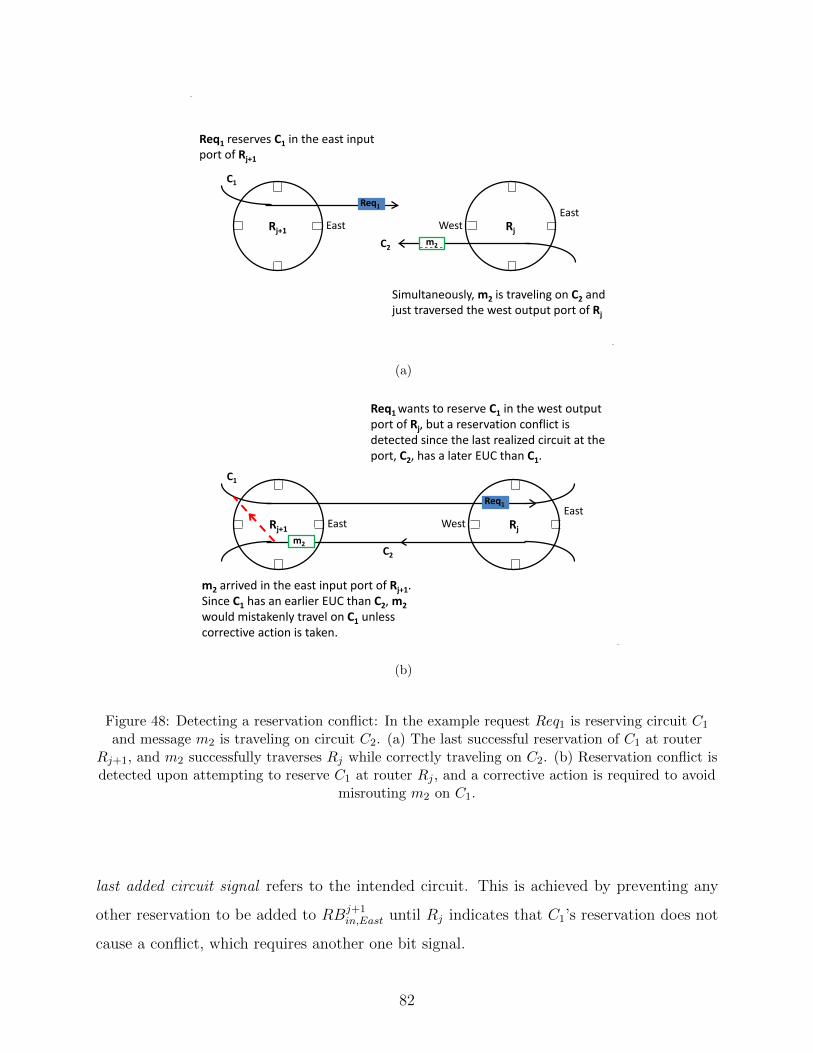
Rj+1 Rj East West
Simultaneously, m2 is traveling on C2 and just traversed the west output port of Rj
East
Req1 reserves C1 in the east input port of Rj+1
C2 m2
Req1
C1
(a)
Rj+1 Rj East West
East
Req1 wants to reserve C1 in the west output port of Rj, but a reservation conflict is detected since the last realized circuit at the port, C2, has a later EUC than C1.
m2 arrived in the east input port of Rj+1. Since C1 has an earlier EUC than C2, m2 would mistakenly travel on C1 unless corrective action is taken.
C2
C1
Req1
m2
(b)
Figure 48: Detecting a reservation conflict: In the example request Req1 is reserving circuit C1
and message m2 is traveling on circuit C2. (a) The last successful reservation of C1 at routerRj+1, and m2 successfully traverses Rj while correctly traveling on C2. (b) Reservation conflict isdetected upon attempting to reserve C1 at router Rj , and a corrective action is required to avoid
misrouting m2 on C1.
last added circuit signal refers to the intended circuit. This is achieved by preventing any
other reservation to be added to RBj+1in,East until Rj indicates that C1’s reservation does not
cause a conflict, which requires another one bit signal.
82

6.2.2 Detecting a Reservation Conflict While a Message is Traversing a Circuit
In Fig. 48 it is possible that m2 – which is traveling on C2 – arrives at FBj+1East before Rj
signals RBj+1in,East to remove C1’s reservation. In this case, C1 may get realized at Rj+1,
thereby misrouting m2 on C1.
To prevent misrouting, Rj+1’s east input port should check that m2 is traveling on the
correct circuit. In general, at any router, Ri, each input port, π, checks that both the
destination and the id of the outstanding request that reserved the currently realized circuit
match those of the next message in FBiπ. To retain one cycle per hop latency on the data
plane, the comparisons of the destination and the id of the outstanding request are performed
in parallel to the message’s head flit traversing the switch to the next router.
Corrective Action: In Fig. 48 if the comparisons indicate that m2 is being misrouted,
Rj+1 stops sending m2 and does not remove m2’s head flit from FBj+1East. As for the input
port on the next router on C1’s path, it will be signaled to discard m2’s head flit as follows:
each router’s input port receives a data valid signal, which indicates whether a flit is being
received during the current cycle. The results of comparing the destination and the id of the
outstanding request are logically ANDED with the data valid signal of the next input port
on the realized circuit’s path. Because the comparison failed, the data valid signal would be
cleared causing the next input port to discard m2’s head flit.
Further, Section 6.2.1 indicates that RBj+1in,East will receive a signal from Rj to remove C1.
However, if misrouting is detected before receiving the signal, the one-flit remove conflicting
circuit message can be sent at the next cycle instead of waiting for the signal from Rj. With
this optimization, RBj+1in,East would have to ignore the next remove circuit signal that Rj
sends.
After sending the remove conflicting circuit message, normal operation of Rj+1 resumes,
which includes: RBj+1in,East finding the next reservation with the earliest EUC (C2 in the
example), realizing that circuit, and sending the buffered message on the circuit (sending m2
on C2).
83

(a)
(b)
Figure 49: A circular dependency that causes deadlock. The events are numbered to help explainhow the deadlock develops.
84

6.3 AVOIDING DEADLOCK
In the proposed scheme, each of the control and data planes can be designed to avoid
deadlock. A 2D mesh topology is assumed where the control plane uses X-Y routing and
the data plane uses Y-X routing. The routers of the data plane have two different kinds
of buffers: flit buffers for storing messages (or packets), and reservation buffers for storing
circuit reservations. These two types of buffers have a dependence relationship. On the
data plane, messages travel on circuits, which require space in the circuit reservation buffers.
Similarly, new reservations require free space in the RBs. RB space becomes available only
when messages are able to advance so that circuit reservations are utilized and removed
from the RBs. Because circuits are reserved backwards; from destination to source, a circular
dependency may develop causing potential deadlock in the NoC, as in the following scenario:
In Fig. 49, a data request is attempting to reserve a new circuit, C1. Unfortunately, when
the request arrives at router Ra, there is no free space in the RB of C1’s required input port,
RBain,North. If the request waits, free space may become available allowing C1 to be reserved
and allowing the request to advance to its destination. Free space becomes available only if
the next message, m, in FBaNorth is able to exit Ra, thus making room for C1’s reservation.
However, m may be blocked and unable to advance due to a full buffer at the input port
of the next router on m’s path. Let m2 be the message at the head of the chain of blocked
messages and assume that m2 is stopped at router Rz and is traveling on circuit C2. A
circular dependency occurs if m2 is unable to move because C2 cannot be realized at Rz
before the new circuit being reserved, C1, is consumed at the same router, Rz. An example
of this might be if C1 and C2 share the west output port at Rz, and C1 has an earlier EUC
than C2. It can be detected that a deadlock may have developed if a request is unable to
reserve a circuit due to unavailability of RB space and this situation persists for a specified
number of cycles (i.e., a timeout mechanism).
Resolving this potential deadlock is similar to handling a reservation conflict (Sec-
tion 6.2.2): the router at which the request is unable to make the reservation (Ra in Fig. 49)
signals the last input port’s RB at which C1 was successfully reserved to mark C1 for re-
moval, and the request is allowed to proceed to its destination without reserving C1, thus
85

breaking the deadlock. Note that C1’s reservation in the signaled RB is not necessarily the
one with the earliest EUC. Consequently, C1’s reservation may not be released immediately;
rather it is marked for removal so that when it becomes the earliest one in the RB, a remove
conflicting reservation message is injected to consume the partially reserved C1.
6.4 IMPROVING QUALITY OF ESTIMATION
Inaccuracy in estimating circuit utilization times may hurt resource utilization and intercon-
nect performance. Specifically, if an estimation is too optimistic assuming that a circuit, Ci,
would be utilized much sooner than actually occurs, a message traveling on another circuit
sharing a sub-path with Ci but scheduled later than Ci may be delayed until Ci is utilized.
Conversely, if an estimation is too pessimistic assuming Ci would be utilized much later
than what actually happens, the message traveling on Ci may suffer delays if circuits sharing
sub-paths with Ci but having earlier EUCs are reserved; as these circuits would be realized
before Ci on the shared sub-paths even though Ci arrives first.
Obtaining an accurate EUC can be reduced to determining a good mechanism for esti-
mating round-trip times for satisfying requests. The request and reply travel times depend
on network conditions, while the request processing time depends on the status of the re-
quested line in the cache, which can cause great variability in the request processing time.
For example, a request that hits in the cache takes much less time to send the data reply
than if the request misses and the line has to be retrieved from the off-chip memory. Large
variability in request processing times can greatly affect the accuracy of EUCs. Therefore,
it is better to restrict estimates to the cases of short request processing times, which should
be the the typical case for an efficient cache design.
When the request requires long processing due to the memory system (e.g., a cache
miss), a release circuit message is immediately dispatched in place of the data reply message
to release the circuit reservation. In this case, another method (e.g., traditional packet
switching) can be used to send the data reply message. To keep the data plane circuit
switched, a forward FCFS reservation (Deja Vu switching; Chapter 5) is used for reserving
86

the reply’s circuit when the reply is ready (supporting forward circuits as a fallback for
reverse circuits is discussed in Section 6.5). Focusing on replies with short processing times
reduces the variability in round-trip times primarily induced by the memory system, and
makes estimates dependent mainly on network conditions.
An intuitive estimate of the round-trip time from node A to node B utilizes previously
observed round-trip times. Alternative methods exhibit different trade-offs between quality
of estimation and hardware resources. For example, each node may keep a per hop estimate
that is the average of: the current per hop estimate and the last observed per hop latency
(the last observed round-trip time to any destination normalized per hop). Similarly, a node
may keep a running average per destination, or even more information.
However, when high traffic load causes the estimated round-trip times to be large, inaccu-
racy of the EUC can become amplified. In such cases, the benefit of early circuit reservation
is often outweighed by the potentially poor resource preallocation due to the inaccuracy in
the round-trip time estimation. Therefore, it is proposed to cap estimates by a factor of the
minimum round-trip time, such that an estimate greater than the cap value does not reserve
a circuit for the reply. For example, if the zero-load round-trip time from A to B is 30 cycles
and the maximum cap factor is two, then for any estimate greater than 60, A’s request does
not reserve the circuit for the reply. In these cases Deja Vu switching is chosen as a fallback
for reserving the reply’s circuit.
6.5 HANDLING CASES WHEN CIRCUIT PRE-ALLOCATION IS NOT
POSSIBLE
There are cases when circuit pre-allocation is not possible. For example, write-back messages
sent upon evicting a dirty cache line are not preceded by a request, hence there are no pre-
allocated circuits for such messages. Additionally, data request messages may not always
reserve circuits. For example, when sending a data request if there is not a good estimate for
when the reply data message will arrive at the requester, it may be better not to pre-allocate
a circuit (Section 6.4).
87

VC1
VCn
…..
Input Buffers Crossbar Switch
Route Computation
VC Allocator
Switch Allocator
Input 0
Input 4
. . . . . .
Output 0
Output 4
. . . . . .
Crossbar Switch
Matching
Input 0
Input 4
. . . .
Output 0
Output 4
. . . .
i/p Ports FCFS Res.
Buffers
o/p Ports FCFS Res.
Buffers
. . .
Data Plane Router
Control Plane Router
VC1
VCn
…..
Input Buffers
. . .
Matching
. . .
. . .
o/p Ports Reverse
Res. Buffers
i/p Ports Reverse
Res. Buffers
Arbitration
VC1 VC2
VC1 VC2
Figure 50: Diagrams of the control and data plane’s routers with support for both forward andreverse reservations.
There are also cases when a circuit is partially or completely reserved but should be
removed. For example, when a request misses in the cache, the requested cache line is
fetched from the off-chip memory, which takes a relatively long time. If this request’s circuit
is kept until the line is fetched, it can delay the realization of other circuits, which hurts
performance; instead a message should be dispatched in place of the data reply message
to utilize and remove the circuit. Another example is a reservation conflict (see Section
6.2), which – although rare – may occur while reserving a new circuit. If not handled, a
reservation conflict can cause misrouting of already in-flight data messages; thus the partial
reservation of the new circuit need to be removed. In all the above cases the data messages
still need to be sent, and because the data plane is designed to be circuit switched, Deja Vu
88

switching is chosen as the fallback mechanism for reserving circuits. This section explains
how the reverse and forward reservations are simultaneously supported in the NoC.
There are two main distinctions between reverse and forward reservations: the direction
of reserving the circuit and the order of circuit realization. These distinctions require the
reverse and forward reservations be separated and require that the packets traveling on these
two types of reserved circuits be separated as well. I.e., each port maintains future reverse
and forward reservations in separate buffers, and two virtual channels (VCs) are required
on the data plane, one for packets traveling on reverse circuits and the other for packets
traveling on forward circuits. Configuring the crossbar of a data plane router is based on
the result of matching either: reverse reservations having the earliest EUCs in the RBs of
the input and output ports (Section 6.1.3), or the heads of forward reservation queues of
input and output ports – since the forward reservations are already queued in their order
of realization. To improve the quality of matching, in each cycle separate matching of the
reverse and forward reservations is carried out with priority given to the decisions of one
of them based on a particular arbitration policy such as round robin. Fig. 50 shows the
architecture of the control and data plane routers which support both kinds of reservations.
The top router depicts the control plane router which is packet switched, and communicates
to the data plane router reverse and forward circuit reservations made by data request and
r -packet (Chapter 5) circuit reservation messages, respectively. The bottom router depicts
the data plane router connected to the control plane router at the same node. It is circuit
switched and has reservation buffers for both reverse and forward circuits, and has two VC
flit buffers at each input port, one for the packets traveling on reverse circuits and one for
packets traveling on forward circuits.
6.6 IMPLEMENTATION ISSUES
To demonstrate hardware implementation feasibility, this section discusses the representation
of EUC and a scheme for keeping track of the current cycle number, as well as breaking ties
between reservations that have equal EUCs.
89

6.6.1 EUC Representation
To minimize the number of bits for representing EUC, time is considered to be composed
of consecutive time intervals of equal lengths, with a counter, CLOCK, recording the cycle
number in the current interval. EUC is a cycle number which is relative to either: the
current (I0), previous (I−1), or the next time interval (I+1) – thus, two bits are sufficient to
represent an interval. At the end of the current interval, I0, CLOCK is reset to 0 and the
intervals of EUCs are shifted, such that EUCs in Ii are now considered to be in Ii−1, where
i ∈ {+1, 0,−1}. For example, assume that the length of the time interval is 1024 cycles and
assume that a router, Ra, on the data plane has a reservation, Resk, with EUC = 1020 in
I0. Also, assume that when I0 ends, some router, Rb, on the control plane has a request,
Reql, carrying an EUC of 26 in I+1. When I0 ends, CLOCK is reset to 0, Resk’s EUC in Ra
becomes 1020 in I−1, and the EUC carried by Reql becomes 26 in I0.
I-1 I0 I+1 I-2
Current Interval
Figure 51: Tracked time intervals. All reservations falling in I−2 are maintained in ascendingorder in the reservation buffers.
To handle the case that a circuit reservation may age to be in a time interval older that
I−1, the time before I−1 is considered as one infinite interval, I−2 (See Fig. 51). Reservations
in I−2 are realized before the reservations in other time intervals. Reservations that age
and become in I−2 are kept in the sequential order of their realization while their EUCs are
discarded. I.e., if at an RB one or more circuit reservations age and become in I−2, these
reservations are ordered relative to each other using their EUCs, and then added after any
reservations that are already in I−2.
Because EUCs for reservations held in I−2 are not retained, it is necessary to guarantee
that no data request can insert a new reservation in I−2. The first step to achieve this
guarantee is choosing an appropriate length, T , of the time intervals. Let M be the maximum
90

acceptable round-trip time (in cycles) between any two nodes. By choosing T to be at least
M cycles, no request can insert a reservation in an interval beyond I+1 in the future, and
choosing T to be at least 2M cycles reduces the probability that a request will attempt to
insert a reservation in I−2. To eliminate this probability, a request should stop reserving a
circuit if the reservation will be in I−2, as follows.
A request’s carried EUC continues to be decremented by one cycle per hop as the request
advances to its destination. When a request is sent, its initial carried EUC can be in either
I+1 or I0. Thus, if the current time interval ends and the request’s carried EUC becomes
in I−2 due to a severely delayed reservation packet, this indicates that the request’s carried
EUC is now very inaccurate. In such a case, the request’s partially reserved circuit should
be removed while allowing the request to proceed without reserving the remainder of the
circuit. The partial circuit is removed in the same way a circuit is removed when a potential
deadlock is detected (Section 6.3).
6.6.2 Breaking Ties
It may happen that two different requests reserve two circuits with equal EUCs across the two
circuits’ shared ports. There is a need to guarantee a consistent ordering of realizing these
two circuits on their shared sub-path. To enforce a total ordering, two pieces of information –
besides the EUC – are associated with a circuit’s reservation: (1) the number of the circuit’s
destination node, dnode ∈ {d0, ..., dN−1}, where N is the number of nodes in the network;
and (2) the id, rid, of the outstanding request at dnode that reserved the circuit, such that
rid ∈ {0, ..., s}, where a node can have at most s outstanding requests. If two circuits C1 and
C2 have equal EUCs, the tie can be broken by comparing their destination nodes (there is
a total ordering of destination nodes), and if they share the same destination, tie is broken
by comparing their request ids. Tie breaking can be simplified to having to compare only
destination nodes when EUCs are equal while enforcing that a requesting node does not
issue two or more requests with identical EUCs.
91

6.7 DISCUSSION: USING RED CARPET ROUTING FOR SAVING
POWER
Chapter 5 demonstrates the use of Deja Vu switching for reducing power consumption with-
out sacrificing performance. Section 5.4 presents the analysis relating performance to the
reduced data plane speed. The same analysis can be applied to Red Carpet Routing for
saving power. However, the are differences that should be considered: (1) Circuits reserved
by data requests inherently satisfy the first constraint (Section 5.4.1), which requires that
data packets do not catch up to their circuit reservations. (2) With Red Carpet Routing
there are still cases when forward reserved circuits (i.e., Deja Vu switching) need to be used
(Section 6.5). Therefore, the slow down of the data plane must ensure that forward reserved
circuits also satisfy the first constraint (Section 5.4.1). (3) In the case of a cache optimized
for speed, the relatively small lead time of detecting a cache hit over reading the cache line
may require a relatively large slow-down factor to ensure that data packets do not catch up to
their forward reservations. (4) In a system where power consumption is an important design
constraint, it is less likely that the cache be optimized for speed, in which case using Deja Vu
switching – as demonstrated in Chapter 5 – alone is probably more efficient in saving power
since there is no overhead for supporting the backward reservations. For these reasons, this
chapter focuses on evaluating the performance benefit of Red Carpet Routing in a CMP
with a fast cache, while also providing an evaluation of the effect on power consumption of
such a system.
6.8 EVALUATION OF PROACTIVELY ALLOCATED CIRCUITS
The proposed proactive circuit allocation scheme, or Red Carpet Routing (RCR) is evaluated
through simulations of benchmarks from the SPLASH-2 [92], PARSEC [15], and Specjbb [90]
suites using the functional simulator Simics [86]. The simulated CMP has 16-core with 3 GHz
UltraSPARC III in-order cores with instruction issue width of three. Each core has private
16 KB L1 data and instruction caches with an access latency of one cycle. The CMP has a
92

distributed shared L2 with 1MB per core. Cache lines are 64 bytes, and each is composed
of eight 8-byte words. Cache coherency is maintained with the MESI protocol. A stalled
instruction waiting for an L1 miss to be satisfied is able to execute once the critical word
is received, which is sent as the first word in the data reply packet. The cache is assumed
to be optimized for fast access. From Cacti [18], at 3 GHz and 32nm technology the access
cycles of the L2 tag and data arrays are two and four cycles, respectively, for a 1MB L2 per
tile partitioned into two banks. The NoC’s topology is a 2D mesh.
A CMP with the RCR NoC is evaluated against CMPs with: (1) a purely packet switched
NoC (PKT), (2) the Deja Vu switching NoC (DV), which uses forward circuit reservations
(Chapter 5), and (3) a zero-overhead Ideal NoC. Each of the evaluated NoCs is composed of
two planes: a control plane that carries control and cache coherency messages, and a data
plane that carries data messages. The control plane is packet switched in all four NoCs,
while the data plane is only packet switched in the PKT NoC and circuit switched in the
other three NoCs. In the data plane of the Ideal NoC all possible circuits are assumed to
simultaneously exist, such that all the circuit switched flits experience only one-cycle per hop
without suffering any network delays due to contention. The configuration of the simulated
NoCs is described below.
Packet Switching and Message Sizes The simulated packet switched routers have
a three cycle router pipeline. In general, messages on the control plane are one flit long,
while messages on the data plane are five flits long. For RCR, data request messages may
be composed of either one or two flits. If the request will reserve a circuit for its reply, the
request message is composed of two flits due to the additional space required to carry the
circuit’s EUC; otherwise it is composed of one flit.
Virtual Channels The control plane has four virtual channels (VCs). Control plane
routers have a FIFO buffer for two packets per VC per input port. The data plane of PKT,
DV, and the Ideal NoCs, each has only one channel for data messages, while the data plane
of the proposed RCR NoC has two VCs, one for the messages traveling on reverse circuits
and one for the messages traveling on forward circuits. The routers of the data plane have
a FIFO buffer for two data packets per input port. In the case of RCR, the FIFO buffer of
each VC can hold one data packet.
93

Circuit Reservation Buffers In the RCR NoC, each router port has two circuit reser-
vation buffers, one for the reverse and one for the forward reservations. The buffers can hold
12 reverse reservations and 5 forward reservations, per port. In the DV NoC, each port has
only one buffer for forward reservations with size set to 17, the total number of reservations
a port on the RCR NoC can store.
Estimating Round-Trip Time At the requesting node the round-trip time is estimated
by computing the median of the last observed three round-trip times for the request message’s
destination. However, large estimates tend to be inaccurate which hurts performance (See
Section 6.4). To reduce such inaccurate estimates, a data request message reserves a circuit
only if the estimate is at most X times the minimum round-trip time. After experimenting
with the design space, X is set to 2.
0.70
0.75
0.80
0.85
0.90
0.95
1.00
barnes
lu con
tig
ocean
radiosity
raytrace
water sp
atial
bodytrack
fluidanim
ate
lu non
contig
water nsquared
blackscholes
specjbb
radix
cann
eal
Average
DV RCR Ideal
Average L2 H
it Laten
cy Relative to
the
CM
Pwith
PKT
NoC
Figure 52: Average L2 hit latency normalizedto the purely packet switched system (the
Y-axis starts at 0.7).
1.00
1.04
1.08
1.12
1.16
1.20
1.24
barnes
lu con
tig
ocean
radiosity
raytrace
water sp
atial
bodytrack
fluidanim
ate
lu non
contig
water nsquared
blackscholes
specjbb
radix
cann
eal
Execution TimeSpeedu
p of CMP with
Ideal
NoC
over the
CMP with
PKT
NoC
Figure 53: Identification of communicationsensitive benchmarks by examining the
execution time speedup using the Ideal NoC(the Y-axis starts at 1.0)
6.8.1 Performance Evaluation
The parallel section of each benchmark is simulated. First comparison considers the average
latency of satisfying an L1 miss that hits in the L2, or simply the average L2 hit latency,
which is essentially the average round-trip time for sending a request that hits in the L2 and
receiving its reply. Fig. 52 shows the average L2 hit latency of the three CMPs: (1) with
the DV NoC; (2) with the RCR NoC; and (3) with the Ideal NoC. The results displayed in
all the figures are relative to the CMP with the purely packet switched NoC (PKT). With
94

the DV NoC there is only a modest improvement in the L2 hit latency, while with the RCR
NoC there is a significant improvement for almost all the benchmarks except for a couple of
benchmarks (the contiguous version of LU and Water Spatial did not benefit from the RCR
NoC).
Since the execution time of each benchmark may not be sensitive to the communication
latency over the NoC, the execution time speedup achievable with the Ideal NoC (Fig. 53) is
examined and the benchmarks are classified into two groups: communication sensitive with
a speedup of at least 4% and communication insensitive with a speedup of less than 4%.
Based on this classification the execution time speedup achievable with the DV and RCR
NoCs is compared in Fig. 54. The speedups of the communication sensitive benchmarks
are displayed on the right side of the chart. The system with DV achieves an average
speedup of only 2% over the system with PKT. The system with RCR achieves up to 16%
speedup (Raytrace and Specjbb), with an average of 8% over the system with DV, and an
average of 10% over the system with PKT. On the left side of the chart the speedups of the
communication insensitive benchmarks are displayed. With DV there is almost no speedup,
while with RCR there is a nominal speedup (2%, on average).
1.00
1.04
1.08
1.12
1.16
lu con
tig
water sp
atial
fluidanim
ate
water nsquared
radix
cann
eal
Average
barnes
ocean
radiosity
raytrace
bodytrack
lu non
contig
blackscholes
specjbb
Average
DV RCR
Execution Time Spe
edup
Over the CMP
with
PKT
NoC
Figure 54: Execution time speedup of CMPswith the DV and RCR NoCs (the Y-axis startsat 1.0). Communication sensitive benchmarks
are displayed on the right of the chart.
0%
20%
40%
60%
80%
100%
barnes
lu con
tig
ocean
radiosity
raytrace
water sp
atial
bodytrack
fluidanim
ate
lu non
contig
water nsquared
blackscholes
specjbb
radix
cann
eal
Average
DV RCR
Percen
tage
Achieved of the Id
eal
Performan
ce
Figure 55: Percentage achieved of theperformance of the CMP with the ideal NoC.
Fig. 55 shows how much of the potential execution time speedup achievable with the
Ideal NoC that the systems with the DV and RCR NoCs achieve. The CMP with DV gains
95

only between 1% to 24%, with an average of 12%, compared with the ideal case, while the
CMP with RCR gains much more; between 40% and 89%, with an average of 68%.
6.8.1.1 Round-Trip Time Estimation This section compares three different methods
for estimating round-trip times: (1) MedianOf3: the requesting node estimates the round-
trip time as the median of the last three observed round-trip times to the destination.
(2) DestinationAvg: each node maintains a running average of the round-trip latency per
destination and uses these averages as the estimates for the round-trip times. (3) HopAvg:
a requesting node maintains a running average of the round-trip latency normalized per hop
for all messages returning to the requesting node, and uses it to estimate the round-trip
latency to any destination. Fig. 56 compares the execution time speedup of the proposed
scheme using each of the three methods for the communication sensitive benchmarks. Little
differences are observed between the three estimation methods, except in the case of Specjbb
where the MedianOf3 greatly out performs the other two.
1.00
1.05
1.10
1.15
1.20
barnes
ocean
radiosity
raytrace
bodytrack
lu noncontig
blackscholes
specjbb
Average
MedianOf3 DestinationAvg HopAvg
Execution Tim
e Speedup Over the
CMP with PKT
Figure 56: Comparing the execution timespeedup with different round-trip times
estimation methods.
0%5%
10%15%20%25%30%35%
lu con
tig
water sp
atial
fluidanim
ate
water nsquared
radix
cann
eal
barnes
ocean
radiosity
raytrace
bodytrack
lu non
contig
blackscholes
specjbb
% Potential Deadlock % Conflict Reservations % Released Circuits ‐ Dueto Long Processing
Figure 57: Percentage of released circuitsrelative to the number of requests performing
circuit reservations.
6.8.1.2 Forward Circuits as a Fallback As mentioned in Section 6.5, there are situ-
ations that require releasing reverse circuit reservations. Fig. 57 examines the percentage
of released circuits relative to the number of circuit reservations. It was found that the
majority of circuits are released due to long processing times (upon a cache miss to the off-
chip memory), which can reach more than 25% for several applications. The percentage of
96

circuits released due to potential deadlocks and reservation conflicts represent a very small
percentage of less than 3% and 2% of circuit reservations, respectively.
When reverse circuits are released, forward circuits are used. Additionally, forward
circuits are used when data requests do not reserve circuits due to round-trip estimates
that exceed the stated threshold (2 times the minimum round trip time) and for write-back
messages of modified cache lines. Sending messages to release circuits can increase the traffic
volume, however, it was found that this increase is small. Specifically, assuming flit sizes of
6- and 16-bytes on the control and data planes, respectively, the percentage increase in traffic
volume in the RCR NoC compared to the DV NoC is 2%, on average, for the communication
sensitive benchmarks (Fig. 58).
0%
1%
2%
3%
4%
5%
6%
7%
lu contig
water spatial
fluidanim
ate
water nsquared
radix
canneal
Average
barnes
ocean
radiosity
raytrace
bodytrack
lu noncontig
blackscholes
specjbb
Average
Percentage increase in traffic volume on RCR NoC relative to DV NoC
Figure 58: Percentage increase of flits sent over the RCR NoC compared to the DV NoC.
Fig. 59 compares the energy of the RCR NoC normalized to the energy of the DV NoC.
The communication insensitive benchmarks (left of the chart) experience increased NoC en-
ergy with the RCR scheme. The reason for the increase is due to the power overhead of the
RCR scheme, such as the circuit reservation buffers and the roundtrip time estimations, but
the benefit in execution time is modest (1.5% on average). On the other hand, the communi-
cation sensitive benchmarks (right of the chart) sometimes show an increase and sometimes
a decrease in NoC energy with the RCR scheme. The increase or decrease in energy depends
on whether the power overhead of the RCR scheme is outweighed by the gain in execution
speedup. Note, however, that the chart compares only the NoC energy, not the CMP energy
consumption, which is estimated next. Considering that the average increase in NoC energy
97

0.90
0.95
1.00
1.05
1.10
lu
water spatial
fluidanim
ate
water nsquared
radix
canneal
Average
barnes
ocean
radiosity
raytrace
bodytrack
lu noncontig
blackscholes
specjbb
Average
Norm
alized
RCR N
oC Energy to D
V
Figure 59: Normalized energy of the RCR NoC to the DV NoC.
is about 0.6% and 5.5%, for the communication sensitive and insensitive benchmarks, respec-
tively, and that their average speedups are about 8% and 1.5%, respectively, and assuming
that the NoC power budget is about 25%, on average, of the CMP power budget [42, 73], the
CMP energy is estimated to decrease by 5.4% for the communication sensitive benchmarks,
and increase by 0.27% for the communication insensitive benchmarks.
6.9 CONCLUSION
Circuit switching is effective in speeding up communication when the overhead of setting up
circuits is reduced or amortized with re-use of circuits. This chapter proposes a proactive
scheme for circuit allocation to completely hide the circuit setup overhead for reply messages
by having the request messages reserve the circuits for their anticipated replies. Reserving
circuits by requests requires time-based reservations to avoid holding NoC resources unnec-
essarily idle which under-utilizes the NoC. However, variability in network traffic conditions
and request processing times make it impossible to use accurate time-based reservations.
Hence, approximate time-based reservations are used by estimating the round-trip time
from the time when a request is sent until its reply is received. The benefit of the design is
demonstrated through simulations of parallel benchmarks. For a CMP with a fast on-chip
98

cache the proposed scheme enables execution time speedup of up to 16% and an average of
about 10% over the purely packet switched NoC; and performs better than the proposed for-
ward reservations scheme (Chapter 5) by up to 16% and an average of 8%. In addition, this
execution speedup translates into an average 5.4% decrease in the CMP energy consumption
over the Deja Vu switching NoC.
99

7.0 SUMMARY AND CONCLUSION OF THE THESIS
The network-on-chip is critical to both the performance and power consumption of chip
multiprocessors since it carries the data and cache coherency traffic exchanged among the
processing cores and on-chip cache memory. In general purpose CMPs any pair of inter-
connect nodes may need to communicate, hence supporting all-to-all communication is a
definite requirement of the network-on-chip. Packet switching achieves this requirement,
but as its name suggests, requires each interconnect node to examine each passing packet
and make appropriate routing decisions. Unfortunately, examining and routing packets adds
a communication latency overhead. Circuit switching, on the other hand, does not suffer
from this routing overhead once circuits are established. However, configuring circuits incurs
time overhead, making circuits only beneficial if the configuration overhead is removed or
amortized. This thesis proposes different techniques that exploit properties of the on-chip
cache traffic to efficiently pre-configure circuits and demonstrates their benefits in improving
performance and/or power consumption.
More specifically, the thesis first proposes a pinned circuit configuration policy for exploit-
ing communication locality in the traffic – where there are pairs of frequently communicating
nodes – to improve communication latency, while coping with changes in communication pat-
terns through periodic reconfiguration. In simulations the pinned circuit configuration policy
improves communication latency by 10%, on average, over on-demand circuit configuration.
In addition, the stability of circuit configurations over a period of time allows routing on par-
tial circuits, which further boosts the utilization of circuits, adding another 10% for a total of
20% improvement in communication latency over the simple on-demand circuit configuration
policy.
Next, the thesis proposes a locality-aware cache design, Unique Private, specifically tar-
100

geting NoCs that exploit communication locality to optimize the NoC performance. The
goal is to create a positive interaction between the cache and NoC that results in reducing
the traffic volume and promoting communication locality in the interconnect, consequently
allowing the processing cores to enjoy faster on-chip communication and faster data ac-
cess. Simulations of scientific and commercial workloads show that using the Unique Private
cache organization and a hybrid NoC employing the pinning circuit configuration policy en-
ables a speedup of 15.2% and 14% on a 16-core and a 64-core CMP, respectively, over the
state-of-the-art NoC-Cache co-designed system which also exploits communication locality
in multithreaded applications.
Third, the thesis proposes Deja Vu switching, a fine-grained circuit configuration ap-
proach that leverages the predictability of data messages to configure circuits on-demand,
and is applied for saving power in multi-plane NoCs. With a control plane dedicated for
the coherence and control messages, and a data plane dedicated for the data messages, a
circuit configuration message is sent as soon as a cache hit is detected and before the cache
line is read. The lead time of the circuit configuration message helps hide the configuration
overhead. By making the data plane completely circuit switched, the faster communication
on these on-demand circuits enables reducing the data plane’s voltage and frequency to re-
duce the NoC’s power. An analysis of the constraints that govern how slow the data plane
can operate without degrading performance is presented and used to guide the evaluation of
the proposed design. In simulations, running the data plane at 2/3 the speed of the control
plane maintained system performance while allowing an average savings of 43% and 53% of
the NoC energy in 16-core and 64-core CMPs, respectively.
Finally, because Deja Vu switching is not as effective for improving performance of a
CMP with a fast on-chip cache, the thesis proposed improving CMP performance using a
more proactive approach of on-demand circuits configuration. The CMP is assumed to have
a fast enough on-chip cache such that the time between detecting a cache hit and reading the
cache line is not long enough for Deja Vu switching to hide the circuit configuration overhead.
Instead, a proactive scheme for circuit allocation is proposed in which data request messages
reserve circuits for their anticipated reply data messages; thus hiding the circuit configuration
overhead from the anticipated reply messages. Reserving circuits by requests requires time-
101
based reservations to avoid holding NoC resources unnecessarily idle which under-utilizes the
NoC. However, variability in network traffic conditions and request processing times make
it impossible to use accurate time-based reservations. To solve this problem, approximate
time-based reservations are proposed, where requesting nodes estimate the time length of
the round-trip from the time when a request is sent and until its reply is received, and
these estimates are used for ordering the realization of circuits in the data plane routers.
Simulations demonstrate the benefit of the proposed proactive circuit allocation scheme.
communication sensitive benchmarks show execution time speedup of up to 16% and an
average of about 10%, over purely packet switched NoC, and an average of 8% over pre-
configuring circuits using Deja Vu switching. In addition, this execution speedup translates
into an average 5.4% decrease in the CMP energy consumption compared to using the Deja
Vu switching NoC.
The above proposed coarse- and fine-grained circuit configuration policies, along with
the proposed locality-aware cache design, can all be integrated in the design of the uncore
of chip-multiprocessors. Specifically, a multi-plane NoC architecture can be adopted, where
the NoC is composed of one or more control planes that are dedicated to the cache coherency
and control traffic, and one or more data planes that are dedicated to the data traffic. The
pinning circuit configuration policy can speedup the control planes, since the control traffic
may exhibit locality in communication patterns, which can be further promoted by adopting
the locality-aware Unique Private cache. The data planes, on the other hand, can benefit
from the on-demand or fine-grained circuit configuration policies: Deja Vu switching or Red
Carpet Routing due to the mostly predictable data traffic.
In conclusion, this thesis presents solutions that harmoniously support both packet and
circuit switching, while being applicable to a wide range of CMP design points. The pinning
circuit configuration policy and the locality-aware cache solutions are applicable to general
cache traffic; speeding-up data delivery and CMP performance. On the other hand, the on-
demand circuit configuration solutions, ( Deja Vu switching and Red Carpet Routing), are
applicable to the predictable cache traffic; with the former exploiting circuits for saving power
without sacrificing performance, and the later utilizing circuits for improving performance,
without expanding power consumption. These solutions open up a myriad of future research
102

avenues and applications, as described in the next section.
7.1 FUTURE WORK
This section presents possible research opportunities building on the solutions provided by
the thesis:
Adaptive Routing in NoC Adaptive routing, for example [43, 55, 67, 81, 68], can help
avoid or reduce traffic congestion in the NoC by diversifying the paths between senders and
destinations; thus more evenly distributing traffic on the network links. It may be beneficial
to study applying adaptive routing to circuit switched traffic, such that diverse paths may
alleviate pressure on circuits in the case where few circuits are heavily utilized. An interesting
situation arises when there is interaction between the traffic on different interconnect planes.
For example, in Red Carpet Routing, data requests travel on the control plane reserving
circuits for messages traveling on the data plane.
On-demand configuration of circuits in optical NoCs The continued scaling of
technology enables the integration of many more processing cores on a single chip. Future
chip-multiprocessors may have hundreds or thousands of cores on a single chip, which puts
a greater pressure on both off-chip and on-chip interconnects to provide the cores with the
necessary bandwidth to keep them running. Optical interconnects are considered for both
off- and on-chip communication [40, 61, 12, 77, 11, 10] due to their speeds and wide range
of frequencies [96], which enables very high bandwidths through the use of wave division
multiplexing (WDM) [88, 45, 22, 70, 59].
In such networks, the sender first coverts the electronic packet into light, or the optical
signal, which is then routed through waveguides and microring resonators [96, 95, 62]. Each
waveguide is coupled with one or more microring resonators. When the wavelength of an in-
cident optical signal propagating within the waveguide overlaps a resonant wavelength mode
of a coupled microring, the signal can be partially or entirely removed from the waveguide.
At the receiver, the optical signal is converted back to an electronic packet. Communication
over optical networks requires setting up optical circuits between senders and receivers by
103

setting the appropriate wavelengths of the microring resonators along the circuits paths.
Similar to circuit switching in electronic interconnects, hiding or amortizing the circuit
configuration overhead is crucial to benefiting from optical NoCs. The overhead may be
amortized over a large transfer [77], or through the pinning circuit configuration policy, but
on-demand circuit configuration may also be possible through Deja Vu switching and Red
Carpet Routing. With Deja Vu switching, the sender would need to know that the circuit
has been completely setup by the reservation packet before starting the transmission of the
optical signal, while with Red Carpet Routing the sender will already know whether a data
request has already configured a circuit. The number of available wavelengths would corre-
spond to the size of the reservation buffers in the proposed on-demand circuit configuration
schemes. However, an optical circuit differs in that it must use the same wavelength in all
the microring resonators on the circuit’s path, which is equivalent to adding a circuit reser-
vation in a particular entry in the circuit reservation buffers in the proposed on-demand
circuit configuration schemes. Thus, successful reservation of circuits requires developing a
mechanism to avoid collision of reservations if more than one attempts to reserve the same
wavelength; otherwise performance may suffer if reservation messages are forced to retry or
drop circuit configurations.
Using emerging memory technologies Static random-access memory (SRAM) is
typically used for on-chip memory. Recently, however, Spin-Torque Transfer Magnetic RAM
(STT-MRAM) has emerged as a promising candidate for on-chip memory in future comput-
ing platforms due to its higher density and lower leakage power characteristics. However,
SRAM exhibits faster access latency, especially for write operations than STT-MRAM [94].
To overcome the performance limitation of STT-MRAM, several approaches have been pro-
posed, for example: hybrid memory designs combining the fast SRAM and denser STT-
MRAM for both on-chip caches [93] and NoC buffers [46]; microarchitecture designs for
trading off retention times for better energy and faster access [74, 47]; and replacing SRAM
for the lower level caches (L2/L3 or the last level cache) with STT-MRAM [82, 97, 87] since
access latencies of lower level caches are typically higher and the bigger sized cache offered
by the higher density of STT-MRAM can have an overall positive effect on performance.
An interesting approach that may be investigated is the effect of faster communication
104

through circuit switching in reducing the effect of higher access times of STT-MRAM, and
even potentially enabling a greater retention time if needed. In particular, packets traveling
on circuits only need to be buffered when blocked by earlier circuit reservations or packets
ahead of them. Thus, the leakage power of the buffers can be significantly reduced if the
SRAM buffers are replaced with STT-MRAM, while circuit switching can help maintain the
same system performance despite the higher access latencies of the buffers in this case.
105

BIBLIOGRAPHY
[1] A. Abousamra, A. K. Jones, and R. Melhem. Proactive circuit allocation in multiplanenocs. In Proceedings of the 50th Annual Design Automation Conference, DAC ’13,pages 35:1–35:10, New York, NY, USA, 2013. ACM.
[2] A. Abousamra, R. Melhem, and A. Jones. Winning with pinning in NoC. In HighPerformance Interconnects, 2009. HOTI 2009. 17th IEEE Symposium on, pages 13–21, aug. 2009.
[3] A. Abousamra, R. Melhem, and A. Jones. Deja vu switching for multiplane NoCs. InNetworks on Chip (NoCS), 2012 Sixth IEEE/ACM International Symposium on, pages11–18, 2012.
[4] A. K. Abousamra, A. K. Jones, and R. G. Melhem. NoC-aware cache design formultithreaded execution on tiled chip multiprocessors. In Proceedings of the 6th Inter-national Conference on High Performance and Embedded Architectures and Compilers,HiPEAC ’11, pages 197–205, New York, NY, USA, 2011. ACM.
[5] K. Asanovic, M. Zhang, M. Zhang, and K. Asanovi. Victim migration: Dynamicallyadapting between private and shared cmp caches. http://hdl.handle.net/1721.1/
30574.
[6] M. Awasthi, K. Sudan, R. Balasubramonian, and J. Carter. Dynamic hardware-assistedsoftware-controlled page placement to manage capacity allocation and sharing withinlarge caches. In High Performance Computer Architecture, 2009. HPCA 2009. IEEE15th International Symposium on, pages 250–261, 2009.
[7] N. Bagherzadeh and S. E. Lee. Increasing the throughput of an adaptive router innetwork-on-chip (NoC). In Hardware/Software Codesign and System Synthesis, 2006.CODES+ISSS ’06. Proceedings of the 4th International Conference, pages 82–87, 2006.
[8] J. Balfour and W. J. Dally. Design tradeoffs for tiled CMP on-chip networks. InProceedings of the 20th annual international conference on Supercomputing, ICS ’06,pages 187–198, New York, NY, USA, 2006. ACM.
[9] K. Barker, A. Benner, R. Hoare, A. Hoisie, A. Jones, D. Kerbyson, D. Li, R. Melhem,R. Rajamony, E. Schenfeld, S. Shao, C. Stunkel, and P. Walker. On the feasibility of
106

optical circuit switching for high performance computing systems. In Supercomputing,2005. Proceedings of the ACM/IEEE SC 2005 Conference, pages 16–16, 2005.
[10] C. Batten, A. Joshi, J. Orcutt, A. Khilo, B. Moss, C. Holzwarth, M. Popovic, H. Li,H. I. Smith, J. Hoyt, F. Kartner, R. Ram, V. Stojanovic, and K. Asanovic. Build-ing manycore processor-to-dram networks with monolithic silicon photonics. In HighPerformance Interconnects, 2008. HOTI ’08. 16th IEEE Symposium on, pages 21–30,2008.
[11] R. Beausoleil, J. Ahn, N. Binkert, A. Davis, D. Fattal, M. Fiorentino, N. P. Jouppi,M. McLaren, C. Santori, R. S. Schreiber, S. Spillane, D. Vantrease, and Q. Xu. Ananophotonic interconnect for high-performance many-core computation. In High Per-formance Interconnects, 2008. HOTI ’08. 16th IEEE Symposium on, pages 182–189,2008.
[12] R. Beausoleil, P. Kuekes, G. S. Snider, S.-Y. Wang, and R. S. Williams. Nanoelectronicand nanophotonic interconnect. Proceedings of the IEEE, 96(2):230–247, 2008.
[13] B. Beckmann, M. Marty, and D. Wood. ASR: Adaptive selective replication for CMPcaches. In Microarchitecture, 2006. MICRO-39. 39th Annual IEEE/ACM InternationalSymposium on, pages 443–454, 2006.
[14] B. Beckmann and D. Wood. Managing wire delay in large chip-multiprocessor caches.In Microarchitecture, 2004. MICRO-37 2004. 37th International Symposium on, pages319–330, 2004.
[15] C. Bienia, S. Kumar, J. P. Singh, and K. Li. The parsec benchmark suite: Char-acterization and architectural implications. In Proceedings of the 17th InternationalConference on Parallel Architectures and Compilation Techniques, October 2008.
[16] S. Bourduas and Z. Zilic. A hybrid ring/mesh interconnect for network-on-chip usinghierarchical rings for global routing. In Networks-on-Chip, 2007. NOCS 2007. FirstInternational Symposium on, pages 195–204, 2007.
[17] J. A. Brown, R. Kumar, and D. Tullsen. Proximity-aware directory-based coherencefor multi-core processor architectures. In Proceedings of the nineteenth annual ACMsymposium on Parallel algorithms and architectures, SPAA ’07, pages 126–134, NewYork, NY, USA, 2007. ACM.
[18] ”CACTI”. http://quid.hpl.hp.com:9081/cacti/.
[19] J. Camacho and J. Flich. Hpc-mesh: A homogeneous parallel concentrated mesh forfault-tolerance and energy savings. In Proceedings of the 2011 ACM/IEEE SeventhSymposium on Architectures for Networking and Communications Systems, ANCS ’11,pages 69–80, Washington, DC, USA, 2011. IEEE Computer Society.
107

[20] F. Cappello and C. Germain. Toward high communication performance through com-piled communications on a circuit switched interconnection network. In Proc. of theInt. Symp. on High Performance Computer Architecture (HPCA), pages 44–53, 1995.
[21] J. Chang and G. Sohi. Cooperative caching for chip multiprocessors. In ComputerArchitecture, 2006. ISCA ’06. 33rd International Symposium on, pages 264–276, 2006.
[22] G. Chen, H. Chen, M. Haurylau, N. Nelson, D. H. Albonesi, P. M. Fauchet, and E. G.Friedman. Predictions of CMOS compatible on-chip optical interconnect. Integration,40(4):434–446, 2007.
[23] L. Cheng, N. Muralimanohar, K. Ramani, R. Balasubramonian, and J. Carter.Interconnect-aware coherence protocols for chip multiprocessors. In Computer Ar-chitecture, 2006. ISCA ’06. 33rd International Symposium on, pages 339–351, 2006.
[24] Z. Chishti, M. Powell, and T. N. Vijaykumar. Optimizing replication, communica-tion, and capacity allocation in CMPs. In Computer Architecture, 2005. ISCA ’05.Proceedings. 32nd International Symposium on, pages 357–368, 2005.
[25] S. Cho and S. Demetriades. Maestro: Orchestrating predictive resource management infuture multicore systems. In Adaptive Hardware and Systems (AHS), 2011 NASA/ESAConference on, pages 1–8, 2011.
[26] S. Cho and L. Jin. Managing distributed, shared L2 caches through OS-level page allo-cation. In Microarchitecture, 2006. MICRO-39. 39th Annual IEEE/ACM InternationalSymposium on, pages 455–468, 2006.
[27] P. Conway, N. Kalyanasundharam, G. Donley, K. Lepak, and B. Hughes. Cache hier-archy and memory subsystem of the AMD Opteron processor. IEEE Micro, 30:16–29,March 2010.
[28] R. Das, S. Eachempati, A. Mishra, V. Narayanan, and C. Das. Design and evaluationof a hierarchical on-chip interconnect for next-generation CMPs. In High PerformanceComputer Architecture, 2009. HPCA 2009. IEEE 15th International Symposium on,pages 175–186, 2009.
[29] S. Demetriades and S. Cho. Barrierwatch: characterizing multithreaded workloadsacross and within program-defined epochs. In Proceedings of the 8th ACM InternationalConference on Computing Frontiers, CF ’11, pages 5:1–5:11, New York, NY, USA,2011. ACM.
[30] S. Demetriades and S. Cho. Predicting coherence communication by tracking syn-chronization points at run time. In Microarchitecture (MICRO), 2012 45th AnnualIEEE/ACM International Symposium on, pages 351–362, 2012.
[31] Z. Ding, R. Hoare, A. Jones, D. Li, S. Shao, S. Tung, J. Zheng, and R. Melhem. Switchdesign to enable predictive multiplexed switching in multiprocessor networks. In Paral-
108

lel and Distributed Processing Symposium, 2005. Proceedings. 19th IEEE International,pages 100a–100a, 2005.
[32] J. Duato, P. Lopez, F. Silla, and S. Yalamanchili. A high performance router archi-tecture for interconnection networks. In Parallel Processing, 1996. Vol.3. Software.,Proceedings of the 1996 International Conference on, volume 1, pages 61–68 vol.1,1996.
[33] N. Enright Jerger, L.-S. Peh, and M. Lipasti. Circuit-switched coherence. In Networks-on-Chip, 2008. NoCS 2008. Second ACM/IEEE International Symposium on, pages193–202, 2008.
[34] A. Flores, J. L. Aragon, and M. E. Acacio. Heterogeneous interconnects for energy-efficient message management in cmps. IEEE Trans. Computers, 59(1):16–28, 2010.
[35] B. Grot, J. Hestness, S. Keckler, and O. Mutlu. Express cube topologies for on-chipinterconnects. In High Performance Computer Architecture, 2009. HPCA 2009. IEEE15th International Symposium on, pages 163–174, 2009.
[36] Z. Guz, I. Keidar, A. Kolodny, and U. C. Weiser. Utilizing shared data in chip mul-tiprocessors with the Nahalal architecture. In Proceedings of the twentieth annualsymposium on Parallelism in algorithms and architectures, SPAA ’08, pages 1–10, NewYork, NY, USA, 2008. ACM.
[37] M. Hammoud, S. Cho, and R. Melhem. Dynamic cache clustering for chip multipro-cessors. In Proceedings of the 23rd international conference on Supercomputing, ICS’09, pages 56–67, New York, NY, USA, 2009. ACM.
[38] M. Hammoud, S. Cho, and R. G. Melhem. ACM: An efficient approach for managingshared caches in chip multiprocessors. In HiPEAC, pages 355–372, 2009.
[39] N. Hardavellas, M. Ferdman, B. Falsafi, and A. Ailamaki. Reactive NUCA: near-optimal block placement and replication in distributed caches. In Proceedings of the36th annual international symposium on Computer architecture, ISCA ’09, pages 184–195, New York, NY, USA, 2009. ACM.
[40] M. Haurylau, G. Chen, H. Chen, J. Zhang, N. Nelson, D. Albonesi, E. Friedman, andP. Fauchet. On-chip optical interconnect roadmap: Challenges and critical directions.Selected Topics in Quantum Electronics, IEEE Journal of, 12(6):1699–1705, 2006.
[41] S. Herbert and D. Marculescu. Analysis of dynamic voltage/frequency scaling in chip-multiprocessors. In Low Power Electronics and Design (ISLPED), 2007 ACM/IEEEInternational Symposium on, pages 38–43, 2007.
[42] Y. Hoskote, S. Vangal, A. Singh, N. Borkar, and S. Borkar. A 5-GHz mesh interconnectfor a teraflops processor. IEEE Micro, 27:51–61, September 2007.
109

[43] J. Hu and R. Marculescu. DyAD - smart routing for networks-on-chip. In DesignAutomation Conference, 2004. Proceedings. 41st, pages 260–263, 2004.
[44] J. Huh, C. Kim, H. Shafi, L. Zhang, D. Burger, and S. Keckler. A NUCA substratefor flexible CMP cache sharing. Parallel and Distributed Systems, IEEE Transactionson, 18(8):1028–1040, 2007.
[45] B. Jalali and S. Fathpour. Silicon photonics. Lightwave Technology, Journal of,24(12):4600–4615, 2006.
[46] H. Jang, B. S. An, N. Kulkarni, K. H. Yum, and E. J. Kim. A hybrid buffer designwith STT-MRAM for on-chip interconnects. In Networks on Chip (NoCS), 2012 SixthIEEE/ACM International Symposium on, pages 193–200, 2012.
[47] A. Jog, A. K. Mishra, C. Xu, Y. Xie, V. Narayanan, R. Iyer, and C. R. Das. Cacherevive: architecting volatile STT-RAM caches for enhanced performance in CMPs.In Proceedings of the 49th Annual Design Automation Conference, DAC ’12, pages243–252, New York, NY, USA, 2012. ACM.
[48] A. B. Kahng, B. Li, L.-S. Peh, and K. Samadi. Orion 2.0: a fast and accurate NoCpower and area model for early-stage design space exploration. In Proceedings of theConference on Design, Automation and Test in Europe, DATE ’09, pages 423–428,2009.
[49] M. Kandemir, F. Li, M. Irwin, and S. W. Son. A novel migration-based NUCA designfor chip multiprocessors. In High Performance Computing, Networking, Storage andAnalysis, 2008. SC 2008. International Conference for, pages 1–12, 2008.
[50] C. Kim, D. Burger, and S. W. Keckler. An adaptive, non-uniform cache structure forwire-delay dominated on-chip caches. SIGOPS Oper. Syst. Rev., 36(5):211–222, Oct.2002.
[51] C. Kim, D. Burger, and S. W. Keckler. Nonuniform cache architectures for wire-delaydominated on-chip caches. IEEE Micro, 23(6):99–107, 2003.
[52] J. Kim, J. Balfour, and W. Dally. Flattened butterfly topology for on-chip networks. InMicroarchitecture, 2007. MICRO 2007. 40th Annual IEEE/ACM International Sym-posium on, pages 172–182, 2007.
[53] J. Kim, J. Balfour, and W. Dally. Flattened butterfly topology for on-chip networks.Computer Architecture Letters, 6(2):37–40, 2007.
[54] J. Kim, W. J. Dally, and D. Abts. Flattened butterfly: a cost-efficient topology forhigh-radix networks. In Proceedings of the 34th annual international symposium onComputer architecture, ISCA ’07, pages 126–137, New York, NY, USA, 2007. ACM.
110

[55] J. Kim, D. Park, T. Theocharides, N. Vijaykrishnan, and C. Das. A low latency routersupporting adaptivity for on-chip interconnects. In Design Automation Conference,2005. Proceedings. 42nd, pages 559–564, 2005.
[56] T. Krishna, A. Kumar, P. Chiang, M. Erez, and L.-S. Peh. NoC with near-ideal expressvirtual channels using global-line communication. In High Performance Interconnects,2008. HOTI ’08. 16th IEEE Symposium on, pages 11–20, 2008.
[57] A. Kumar, P. Kundu, A. Singhx, L.-S. Peh, and N. Jha. A 4.6Tbits/s 3.6GHz single-cycle NoC router with a novel switch allocator in 65nm CMOS. In Computer Design,2007. ICCD 2007. 25th International Conference on, pages 63–70, 2007.
[58] A. Kumar, L.-S. Peh, P. Kundu, and N. K. Jha. Express virtual channels: towards theideal interconnection fabric. In Proceedings of the 34th annual international symposiumon Computer architecture, ISCA ’07, pages 150–161, New York, NY, USA, 2007. ACM.
[59] G. Kurian, J. E. Miller, J. Psota, J. Eastep, J. Liu, J. Michel, L. C. Kimerling, andA. Agarwal. ATAC: a 1000-core cache-coherent processor with on-chip optical net-work. In Proceedings of the 19th international conference on Parallel architectures andcompilation techniques, PACT ’10, pages 477–488, New York, NY, USA, 2010. ACM.
[60] J. Laudon and D. Lenoski. The SGI origin: A ccNUMA highly scalable server. InComputer Architecture, 1997. Conference Proceedings. The 24th Annual InternationalSymposium on, pages 241–251, 1997.
[61] B. Lee, X. Chen, A. Biberman, X. Liu, I.-W. Hsieh, C.-Y. Chou, J. Dadap, F. Xia,W. M. J. Green, L. Sekaric, Y. Vlasov, R. Osgood, and K. Bergman. Ultrahigh-bandwidth silicon photonic nanowire waveguides for on-chip networks. Photonics Tech-nology Letters, IEEE, 20(6):398–400, 2008.
[62] B. Lee, B. Small, Q. Xu, M. Lipson, and K. Bergman. Characterization of a 4 x 4Gb/s parallel electronic bus to WDM optical link silicon photonic translator. PhotonicsTechnology Letters, IEEE, 19(7):456–458, 2007.
[63] H. Lee, S. Cho, and B. Childers. Cloudcache: Expanding and shrinking private caches.In High Performance Computer Architecture (HPCA), 2011 IEEE 17th InternationalSymposium on, pages 219–230, 2011.
[64] S. E. Lee and N. Bagherzadeh. A variable frequency link for a power-aware network-on-chip (NoC). Integration, 42(4):479–485, 2009.
[65] D. Lenoski, J. Laudon, K. Gharachorloo, A. Gupta, and J. Hennessy. The directory-based cache coherence protocol for the DASH multiprocessor. In Computer Archi-tecture, 1990. Proceedings., 17th Annual International Symposium on, pages 148–159,1990.
111

[66] Z. Li, C. Zhu, L. Shang, R. P. Dick, and Y. Sun. Transaction-aware network-on-chipresource reservation. Computer Architecture Letters, 7(2):53–56, 2008.
[67] M. Majer, C. Bobda, A. Ahmadinia, and J. Teich. Packet routing in dynamicallychanging networks on chip. In Parallel and Distributed Processing Symposium, 2005.Proceedings. 19th IEEE International, pages 154b–154b, 2005.
[68] T. Mak, P. Cheung, K.-P. Lam, and W. Luk. Adaptive routing in network-on-chipsusing a dynamic-programming network. Industrial Electronics, IEEE Transactions on,58(8):3701–3716, 2011.
[69] H. Matsutani, M. Koibuchi, H. Amano, and T. Yoshinaga. Prediction router: A low-latency on-chip router architecture with multiple predictors. IEEE Trans. Computers,60(6):783–799, 2011.
[70] R. Morris and A. Kodi. Power-efficient and high-performance multi-level hybridnanophotonic interconnect for multicores. In Networks-on-Chip (NOCS), 2010 FourthACM/IEEE International Symposium on, pages 207–214, 2010.
[71] R. Mullins, A. West, and S. Moore. Low-latency virtual-channel routers for on-chipnetworks. In Computer Architecture, 2004. Proceedings. 31st Annual InternationalSymposium on, pages 188–197, 2004.
[72] R. Mullins, A. West, and S. Moore. The design and implementation of a low-latencyon-chip network. In Design Automation, 2006. Asia and South Pacific Conference on,pages 6 pp.–, 2006.
[73] J. Owens, W. Dally, R. Ho, D. N. Jayasimha, S. Keckler, and L.-S. Peh. Researchchallenges for on-chip interconnection networks. Micro, IEEE, 27(5):96–108, 2007.
[74] S. P. Park, S. Gupta, N. Mojumder, A. Raghunathan, and K. Roy. Future cache designusing stt mrams for improved energy efficiency: devices, circuits and architecture. InProceedings of the 49th Annual Design Automation Conference, DAC ’12, pages 492–497, New York, NY, USA, 2012. ACM.
[75] L.-S. Peh and W. Dally. Flit-reservation flow control. In High-Performance ComputerArchitecture, 2000. HPCA-6. Proceedings. Sixth International Symposium on, pages73–84, 2000.
[76] L.-S. Peh and W. Dally. A delay model and speculative architecture for pipelinedrouters. In High-Performance Computer Architecture, 2001. HPCA. The Seventh In-ternational Symposium on, pages 255–266, 2001.
[77] M. Petracca, B. Lee, K. Bergman, and L. Carloni. Design exploration of optical in-terconnection networks for chip multiprocessors. In High Performance Interconnects,2008. HOTI ’08. 16th IEEE Symposium on, pages 31–40, 2008.
112

[78] A. Pullini, F. Angiolini, S. Murali, D. Atienza, G. De Micheli, and L. Benini. BringingNoCs to 65 nm. Micro, IEEE, 27(5):75–85, 2007.
[79] C. Qiao and R. Melhem. Reducing communication latency with path multiplexingin optically interconnected multiprocessor systems. Parallel and Distributed Systems,IEEE Transactions on, 8(2):97–108, 1997.
[80] M. Qureshi. Adaptive spill-receive for robust high-performance caching in CMPs. InHigh Performance Computer Architecture, 2009. HPCA 2009. IEEE 15th InternationalSymposium on, pages 45–54, 2009.
[81] R. S. Ramanujam and B. Lin. Destination-based adaptive routing on 2D mesh net-works. In Proceedings of the 6th ACM/IEEE Symposium on Architectures for Network-ing and Communications Systems, ANCS ’10, pages 19:1–19:12, New York, NY, USA,2010. ACM.
[82] M. Rasquinha, D. Choudhary, S. Chatterjee, S. Mukhopadhyay, and S. Yalamanchili.An energy efficient cache design using spin torque transfer (STT) RAM. In Low-Power Electronics and Design (ISLPED), 2010 ACM/IEEE International Symposiumon, pages 389–394, 2010.
[83] S. Sawant, U. Desai, G. Shamanna, L. Sharma, M. Ranade, A. Agarwal, S. Dakshi-namurthy, and R. Narayanan. A 32nm Westmere-EX Xeon R© enterprise processor.In Solid-State Circuits Conference Digest of Technical Papers (ISSCC), 2011 IEEEInternational, pages 74–75, 2011.
[84] J. Shalf, S. Kamil, L. Oliker, and D. Skinner. Analyzing ultra-scale application com-munication requirements for a reconfigurable hybrid interconnect. In Supercomputing,2005. Proceedings of the ACM/IEEE SC 2005 Conference, pages 17–17, 2005.
[85] L. Shang, L.-S. Peh, and N. Jha. Dynamic voltage scaling with links for power op-timization of interconnection networks. In High-Performance Computer Architecture,2003. HPCA-9 2003. Proceedings. The Ninth International Symposium on, pages 91–102, 2003.
[86] ”Simics”. http://www.windriver.com/products/simics/.
[87] C. Smullen, V. Mohan, A. Nigam, S. Gurumurthi, and M. Stan. Relaxing non-volatilityfor fast and energy-efficient STT-RAM caches. In High Performance Computer Archi-tecture (HPCA), 2011 IEEE 17th International Symposium on, pages 50–61, 2011.
[88] R. Soref. The past, present, and future of silicon photonics. Selected Topics in QuantumElectronics, IEEE Journal of, 12(6):1678–1687, 2006.
[89] V. Soteriou and L.-S. Peh. Exploring the design space of self-regulating power-awareon/off interconnection networks. IEEE Trans. Parallel Distrib. Syst., 18(3):393–408,2007.
113

[90] SPEC. Spec benchmarks. http://www.spec.org/.
[91] ”SPLASH-2”. http://www-flash.stanford.edu/apps/SPLASH/.
[92] S. Woo, M. Ohara, E. Torrie, J. Singh, and A. Gupta. The SPLASH-2 programs:characterization and methodological considerations. In Computer Architecture, 1995.Proceedings., 22nd Annual International Symposium on, pages 24–36, 1995.
[93] X. Wu, J. Li, L. Zhang, E. Speight, R. Rajamony, and Y. Xie. Hybrid cache architecturewith disparate memory technologies. In Proceedings of the 36th annual internationalsymposium on Computer architecture, ISCA ’09, pages 34–45, New York, NY, USA,2009. ACM.
[94] X. Wu, J. Li, L. Zhang, E. Speight, and Y. Xie. Power and performance of read-writeaware hybrid caches with non-volatile memories. In Design, Automation Test in EuropeConference Exhibition, 2009. DATE ’09., pages 737–742, 2009.
[95] Q. Xu, S. Manipatruni, B. Schmidt, J. Shakya, and M. Lipson. 12.5 Gbit/s carrier-injection-based silicon micro-ring silicon modulators. Opt. Express, 15(2):430–436, Jan2007.
[96] Q. Xu, B. Schmidt, J. Shakya, and M. Lipson. Cascaded silicon micro-ring modulatorsfor wdm optical interconnection. Opt. Express, 14(20):9431–9435, Oct 2006.
[97] W. Xu, H. Sun, X. Wang, Y. Chen, and T. Zhang. Design of last-level on-chip cacheusing spin-torque transfer ram (STT RAM). Very Large Scale Integration (VLSI)Systems, IEEE Transactions on, 19(3):483–493, 2011.
[98] Y. Xu, Y. Du, B. Zhao, X. Zhou, Y. Zhang, and J. Yang. A low-radix and low-diameter3D interconnection network design. In High Performance Computer Architecture, 2009.HPCA 2009. IEEE 15th International Symposium on, pages 30–42, 2009.
[99] T. Yoshinaga, S. Kamakura, and M. Koibuchi. Predictive switching in 2-D torusrouters. In Innovative Architecture for Future Generation High Performance Processorsand Systems, 2006. IWIA ’06. International Workshop on, pages 65–72, 2006.
[100] X. Yuan, R. Melhem, R. Gupta, Y. Mei, and C. Qiao. Distributed control protocolsfor wavelength reservation and their performance evaluation. The Journal of PhotonicNetwork Communications, 1(3):207–218, 1999.
[101] M. Zhang and K. Asanovic. Victim replication: maximizing capacity while hidingwire delay in tiled chip multiprocessors. In Computer Architecture, 2005. ISCA ’05.Proceedings. 32nd International Symposium on, pages 336–345, 2005.
114


![Exploiting Application-Level Information to Reduce Memory ...maggini.eng.umd.edu/pub/deepaka-yeung.pdf · Virtual Cache Lines (VCL) [20] uses a xed cache block size for normal references,](https://static.fdocuments.net/doc/165x107/5d5b9bd488c993bd048bb480/exploiting-application-level-information-to-reduce-memory-virtual-cache.jpg)