EXPERIMENTAL RESEARCH WORK ON A SUB‐MILLIMETER SPARK‐GAP … · i Abstract This thesis presents...
135
EXPERIMENTAL RESEARCH WORK ON A SUB‐MILLIMETER SPARK‐GAP FOR SUB‐NANOSECOND GAS BREAKDOWN A Thesis presented by FRANCISCO SANTAMARÍA PIEDRAHITA UNIVERSIDAD NACIONAL DE COLOMBIA ELECTRICAL AND ELECTRONIC ENGINEERING DEPARTMENT Bogotá, Colombia 2012
Transcript of EXPERIMENTAL RESEARCH WORK ON A SUB‐MILLIMETER SPARK‐GAP … · i Abstract This thesis presents...

EXPERIMENTAL RESEARCH WORK ON A SUB‐MILLIMETER SPARK‐GAP
FOR SUB‐NANOSECOND GAS BREAKDOWN
A Thesis presented by
FRANCISCO SANTAMARÍA PIEDRAHITA
UNIVERSIDAD NACIONAL DE COLOMBIA ELECTRICAL AND ELECTRONIC ENGINEERING DEPARTMENT
Bogotá, Colombia 2012
EXPERIMENTAL RESEARCH WORK ON A SUB‐MILLIMETER SPARK‐GAP
FOR SUB‐NANOSECOND GAS BREAKDOWN
In partial fulfillment of the requirements for the degree
DOCTOR IN ELECTRICAL ENGINEERING
A Thesis presented by
FRANCISCO SANTAMARÍA PIEDRAHITA
Thesis Adviser
PhD. FRANCISCO JOSE ROMAN CAMPOS
ELECTROMAGNETIC COMPATIBILITY RESEARCH GROUP
ELECTRICAL AND ELECTRONIC ENGINEERING DEPARTMENT UNIVERSIDAD NACIONAL DE COLOMBIA
Bogotá, Colombia 2012
i
Abstract This thesis presents the results of a study developed in a sub‐millimeter spark‐gap. For developing the study, a coaxial pulse generator with an internal spark‐gap was constructed. The design and construction processes and theoretical design parameters of the coaxial generator are presented and discussed. In the design and experimental processes, electrostatic‐, electromagnetic‐ and transmission line‐simulations were carried out, which are described here. Laboratory tests for different gases at different pressure‐distance conditions were carried out, and based on these results some important gas discharge parameters were calculated, evaluated and discussed. The experimental results obtained in the present research work were compared and validated with some of most accepted theoretical and empirical models. Additionally, some models based on the classical ones were proposed in this work and validated by means of simulations and laboratory tests. In this thesis work, a simplified transmission line model of a pulse generator, including its spark‐gap, is also proposed and validated. Based on this model, a generator for a specific application was design, constructed and tested, as it is described in the last part of this thesis. INDEX TERMS: Gas Breakdown, Pulsed power, Arc‐resistance, Spark‐gap

ii
Resumen En esta tesis se presentan los resultados de un estudio desarrollado en un spark‐gap sub‐milimétrico. Para desarrollar el estudio se construyó un generador de pulsos coaxial con un spark‐gap interno. En este documento se presentan y discuten los parámetros teóricos empleados en la etapa de diseño y en el proceso de construcción del generador de pulsos. En el proceso de diseño y en la fase experimental se llevaron a cabo simulaciones electrostáticas, electromagnéticas y de línea de transmisión, las cuales son descritas en esta tesis. Realizaron pruebas de laboratorio con diferentes gases y diferentes condiciones de distancia y presión, y con base en estos resultados se calcularon y analizaron algunos lo principales parámetros de la descarga en gases. Los resultados experimentales obtenidos en el trabajo de investigación se compararon y validaron con algunos de los modelos teóricos y empíricos más aceptados en la literatura. Además, se proponen algunos modelos basados en las ecuaciones clásicas y los resultados experimentales; los cuales son validados mediante simulaciones y pruebas de laboratorio. En esta tesis, también se propone un modelo simplificado de línea de transmisión del generador de pulsos, incluyendo el modelo del spark‐gap. Basándose en este modelo, se diseño construyó y probó un generador para una aplicación específica, tal y como se describe en la última parte de la tesis. DESCRIPTORES CLAVES: Descarga en gases, Potencia pulsante, Resistencia de arco, Spark‐gap

iii
Table of Contents Abstract............................................................................................................................................................... i Table of Contents...........................................................................................................................................iii Table of Figures.............................................................................................................................................vii List of Tables ................................................................................................................................................ xiii Introduction ................................................................................................................................................... xv Chapter 1: Electrical Breakdown.............................................................................................................. 1 1.1 Elementary Processes Related to Ionization of Gases................................................................. 1 1.2 Townsend Mechanism.............................................................................................................................. 2 1.2.1 Electron Avalanche ............................................................................................................................... 3 1.2.2 Secondary Emission of Electrons.................................................................................................... 4 1.2.3 From Self‐Sustained Discharge to Breakdown.......................................................................... 5
1.3 Streamer Mechanism ................................................................................................................................ 6 1.4 Breakdown Voltage.................................................................................................................................... 8 1.4.1 Paschen’s Law......................................................................................................................................... 8 1.4.2 Breakdown in SF6 ................................................................................................................................10
1.5 Self‐Breakdown Spark‐Gaps.................................................................................................................10 1.5.1 Arc Discharge ........................................................................................................................................11 1.5.2 Fundamentals of a Closing Switch................................................................................................11 1.5.3 Rise‐time Limit .....................................................................................................................................13 1.5.4 Models for Resistive Phase Time ..................................................................................................13 1.5.5 Models for Arc‐Resistance ...............................................................................................................15
Chapter 2: Experimental Setup..............................................................................................................19 2.1 Pulse Generator .........................................................................................................................................20 2.1.1 High Voltage Source ...........................................................................................................................20 2.1.2 Pulse Forming Line PFL ....................................................................................................................21 2.1.3 The Spark‐Gap ‐ S‐G............................................................................................................................23 2.1.4 The Transmission Line ‐ TL.............................................................................................................30 2.1.5 Load...........................................................................................................................................................30

iv
2.2 Final Design ................................................................................................................................................ 31 2.3 Measuring system .................................................................................................................................... 33 2.3.1 Diagnostic............................................................................................................................................... 33 2.3.2 Apparatus verification ...................................................................................................................... 34 2.3.3 Measurement Set‐up.......................................................................................................................... 38
2.4 EMTP‐ATP Simulation Process ........................................................................................................... 38 2.5 Summary ...................................................................................................................................................... 43
Chapter 3: Experimental Results ........................................................................................................... 45 3.1 Breakdown Voltage ................................................................................................................................. 45 3.2 Derivative Electric Field Measurements......................................................................................... 47 3.2.1 CST Simulation ..................................................................................................................................... 48
3.3 Post‐processing and Waveform Analysis ....................................................................................... 48 3.3.1 Resistive Phase Time (R) ................................................................................................................ 49 3.3.2 Full Width at Half Maximum (FWHM)........................................................................................ 52 3.3.3 Arc‐resistance (Rarc) ........................................................................................................................... 52
3.4 Pulse Repetition Frequency (PRF) .................................................................................................... 55 3.5 Switching Efficiency ................................................................................................................................ 57 3.6 Summary ...................................................................................................................................................... 58
Chapter 4: Sparkgap Modeling .............................................................................................................. 59 4.1 Comparison of Results and Existing Models ................................................................................. 59 4.1.1 Resistive Phase Time (R) ................................................................................................................ 59 4.1.2 Arc‐resistance (Rarc) ........................................................................................................................... 63 4.1.3 Pulse Repetition Frequency (PRF)............................................................................................... 66
4.2 EMTP‐ATP Modeling and Transmission Line Simulations...................................................... 68 4.3 Summary ...................................................................................................................................................... 71
Chapter 5: Switched Oscillator Design................................................................................................. 73 5.1 SWO Principles and Design .................................................................................................................. 73 5.1.1 SWO Design............................................................................................................................................ 74
5.2 Transmission Line Models (TL).......................................................................................................... 76 5.2.1 Radial Transmission Line (RTL) ................................................................................................... 76 5.2.2 EMTP–ATP Modeling and Transmission Line Simulations................................................ 77
5.3 Effect of the Geometrical Parameters on the SWO Generated Signals ............................... 78 5.3.1 Safety factor (S).................................................................................................................................... 78 5.3.2 Coaxial Transmission Line Length (L)........................................................................................ 79 5.3.3 Inter‐electrode Distance and Pressure ...................................................................................... 80
5.4 Electromagnetic Model (EM)............................................................................................................... 82 5.5 Testing of the SWO................................................................................................................................... 84 5.5.1 Experimental Set‐up .......................................................................................................................... 84 5.5.2 Laboratory Tests ................................................................................................................................. 85
Conclusions .................................................................................................................................................... 87 6.1 Pulse Generator......................................................................................................................................... 87 6.2 Experimental Results.............................................................................................................................. 88 6.3 Spark‐gap Modeling................................................................................................................................. 88 6.4 Switching Oscillator................................................................................................................................. 89 6.5 Final Remarks ............................................................................................................................................ 90

v
Acknowledgements .....................................................................................................................................91 References ......................................................................................................................................................92 Papers...............................................................................................................................................................98 Appendix 1: UHMW_PE Properties.........................................................................................................99 Appendix 2: DDot Sensors ....................................................................................................................100 Appendix 3: Analog Voltmeter Verification.....................................................................................103 Appendix 4: Experimental Data ...........................................................................................................104

vi

vii
Table of Figures Figure 1.1. Free path and mean free path of electrons (Kind et al., 1985) 3 Figure 1.2. Electron generation according to the Townsend mechanism (Kind et al., 1985) 5 Figure 1.3. Representation of field distortion in a gap caused by space charge of an electron
avalanche (Kuffel et al., 2000) 6 Figure 1.4. Representation of the development of the streamer. a. Negative streamer. b.
Positive streamer (Naidu et al., 1996) 7 Figure 1.5. Space charge field (Er) around the avalanche head (Kuffel et al., 2000) 8 Figure 1.6. Measured and calculated Paschen curves for atmospheric air (Bluhm, 2006) 9 Figure 1.7. Range of pressures and operating voltages for some closing switches compared
with the Paschen curve obtained for air for inter‐electrode distance of 3 mm (Bluhm, 2006) 11
Figure 1.8. Voltage, current and power loss in a spark‐gap closing switch (Bluhm, 2006) 12 Figure 1.9. Schematic of breakdown characteristic time (Schaefer et al., 1990) 14 Figure 2.1. Schematic representation of a pulse generator 20 Figure 2.2. Ideal output voltage 21 Figure 2.3. Electric field lines (=const) and Electric potential lines (=const) in a semi‐
infinite‐length parallel plate array in w plane 24 Figure 2.4. Rogoswki profiles from Maxwell’s transformation for different (, ) values.
Blue lines: constant lines. Red lines: constant lines 24 Figure 2.5. Equipotential lines from COMSOL simulation for d = 0.5 mm 25

viii
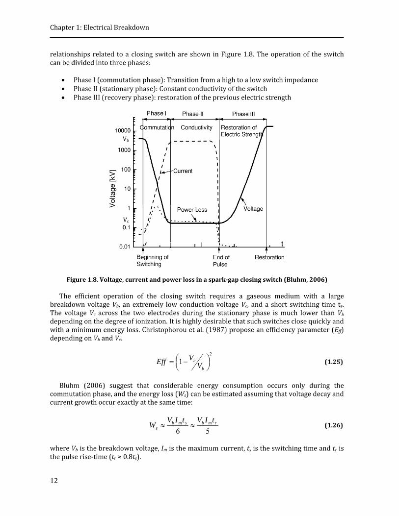
Figure 2.6. Electric field lines from COMSOL simulation for d = 0.5 mm 25 Figure 2.7. Electrode designed with Rogowski profile. a. 3‐D model. b. Electrode dimensions 26 Figure 2.8. Pressurized chamber designed in Inventor 27 Figure 2.9. Details of the spark‐gap. Note the electrodes position, the electrodes and the gas
inlet and outlet 28 Figure 2.10. Geometry and Boundary conditions of the simulation performed in COMSOL 28 Figure 2.11. Structural simulation of the pressurized chamber for p = 1200 kPa 29 Figure 2.12. Schematic diagram of the designed pulse generator. All dimensions in mm 31 Figure 2.13. Constructed pulse generator and its main parts, including the transmission
lines, the electrodes, the pressurized chamber, the 50 M limiting resistor and the 100 load 32
Figure 2.14. Pictures of the electric field sensors (D‐dot) 33 Figure 2.15. Pulse generator. Note the location of the D‐dot sensors, one on the PFL before
the spark‐gap, and the other one on the TL after the spark‐gap 33 Figure 2.16. Average measured breakdown voltage (solid lines) and theoretical breakdown
voltage (dashed lines) as a function of pressure for d = 330 m in air and SF6 35 Figure 2.17. Average measured breakdown voltage (solid line) and theoretical breakdown
voltage (dashed line) as a function of pressure in air with the generator pressurized 36
Figure 2.18. Corrected inter‐electrode distance as a function of pressure based on
measurements 37 Figure 2.19. Average measured breakdown voltage (solid line) and theoretical breakdown
voltage (dashed line) using equation (2.24) as a function of pressure in SF6 37 Figure 2.20. Measurement set‐up. HV source coupled with pulse generator inside shielded
room. Measurement cables connect D‐dots with oscilloscope through SMA connectors in the wall 38
Figure 2.21. EMTP‐ATP Transmission Line model of the pulse generator including PFL and
TL sections, the spark‐gap model (S‐G), a 100 load resistance (R) and the position of the voltage (V) sensors 39
Figure 2.22. Simulated voltages for the air insulated spark‐gap at 774 kPa and d = 450 m.
Green dashed line: Charging voltage before the spark‐gap. Blue line: charging voltage at point of measurement. Blue dotted line: output voltage after the spark‐gap. Red dashed line: output voltage at point of measurement 40

ix
Figure 2.23. Simulated voltages transformed to frequency domain. Green dashed line: Charging voltage before the spark‐gap. Blue line: charging voltage at point of measurement. Blue dotted line: output voltage after the spark‐gap. Red dashed line: output voltage at point of measurement 41
Figure 2.24. Simulated voltages processed in the frequency to correct the displacement from
the points of measurement. Green dashed line: Charging voltage before the spark‐gap (V1). Blue line: input voltage corrected up to the spark‐gap (V1’C). Blue dotted line: output voltage after the spark‐gap (V2). Red dashed line: output voltage corrected up to the spark‐gap (V2’C) 42
Figure 2.25. Voltage drop in the spark‐gap calculated from EMTP‐ATP simulations for air at
774 kPa and d = 450 m. Blue: Expected response (VSG=V1–V2). Red dotted line: Difference between the voltages recorded at the measurement points and the corrected (VSG’=V1’C–V2’C) 42
Figure 3.1. Breakdown voltage measured in air (blue), SF6 (red) and argon (black) at
different pd values 46 Figure 3.2. Breakdown field strength measured in air (blue), SF6 (red) and argon (black) at
different pd values 46 Figure 3.3. Breakdown field strength in air and SF6 at different pd values (Kuffel et al, 2000) 47 Figure 3.4. D‐dot sensors measurements for air at 774 kPa and d = 450 m. Blue line: high‐
voltage side of the spark‐gap switch (D‐dot1). Dashed black line: load‐side of the spark‐gap switch (D‐dot2) 47
Figure 3.5. CST simulated electric fields, for d = 450 m in air. Blue line: Before the spark‐
gap (D‐dot1). Dashed black line: After the spark‐gap (D‐dot2) 48 Figure 3.6. Integrated D‐dot signals for air at 774 kPa and d = 450 m. Blue line: Voltage at
the high‐voltage side of the spark‐gap switch (V1). Dashed black line: Voltage at the load side of the spark‐gap switch (V2) 49
Figure 3.7. Arc‐inductance calculated from measurements and the Braginskii arc‐channel
radius. Green dashed line: d = 320 m. Blue line: d = 450 m 50 Figure 3.8. Resistive phase time for air (blue), SF6 (black) and argon (red) at different pd
values from laboratory tests 51 Figure 3.9. Resistive phase time for air (blue), SF6 (black) and argon (red) at different E/p
values from laboratory tests 51 Figure 3.10. Full Width at Full maximum FWHM for air (blue), SF6 (black) and argon (red) at
different values of pd from laboratory tests 52

x
Figure 3.11. Voltage drop in the spark‐gap together with inductive and resistive voltage for air at 774 kPa and d = 450 m. Red: Corrected voltage drop calculated from signals in Figure 3.6. Green: Inductive voltage. Blue: Resistive voltage 53
Figure 3.12. Resistive voltage drop in the spark‐gap together with current for air at 774 kPa
and d = 450 m. Blue: Resistive voltage. Black: Current 53 Figure 3.13. Arc‐resistance calculated from measurements for air (blue line), SF6 (red line)
and argon (black line) at 774 kPa and 450 m 54 Figure 3.14. Arc‐resistance calculated from measurements for air (blue line), SF6 (red line)
and argon (black line). Pressure between 174 and 674 kPa and d between 330 and 436 m 55
Figure 3.15. Arc‐resistance calculated from measurements for air at different values of pd 55 Figure 3.16. Pulse Repetition Frequency measurement. At least six shots were captured in
the oscilloscope. Td is the time between pulses 56 Figure 3.17. Pulse Repetition Frequency measurement in air. Applied voltage between 5 and
50 kV at different values of pd 56 Figure 3.18. Switching efficiency for air, SF6 and argon at different values of pd. Filled
markers: equation (3.6). Unfilled markers: equation (3.9) 58 Figure 4.1. Resistive phase time for air, from laboratory tests (blue line), Martin’s equation
(red dotted line) and Sorensen and Ristic’s equation (green dashed line) 60 Figure 4.2. Resistive phase time for SF6, from laboratory tests (blue line) and Martin’s
equation (red line) 60 Figure 4.3. Resistive phase time for air. Blue line: laboratory tests, red dotted line: equation
(4.1), black dashed line: equation (4.2) 62 Figure 4.4. Resistive phase time for SF6. Blue line: laboratory tests, red dotted line: equation
(4.1), black dashed line: equation (4.2) 62 Figure 4.5. Resistive phase time for argon. Blue line: laboratory tests, red dotted line:
equation (4.1), black dashed line: equation (4.2) 62 Figure 4.6. Arc‐resistance calculated for air at 774 kPa and 450 m. Measurements (blue
line), Kushner (green line), Sorensen and Ristic (red line), Toepler (black line) and Vlastos (dotted line) 63
Figure 4.7. Arc‐resistance calculated for SF6 and argon at 774 kPa and 450 m.
Measurements (blue line), Kushner (green line), Sorensen and Ristic (red line), Toepler (black line) and Vlastos (dotted line) 64

xi
Figure 4.8. Arc‐resistance calculated for a) air, b) SF6 and c) argon at 774 kPa and 450 m. Measurements (blue line) and modified Kushner’s model (green line) 65
Figure 4.9. Charging voltage (blue line) and voltage for subsequent discharges at different
values of pressure and applied voltage. a) Vg = 50 kV. b) Vg = 10 kV. Notice the inverse relationship between the PRF and voltage level 67
Figure 4.10. Pulse Repetition Frequency in air at 98.4 kPa_mm (blue), 186.8 kPa_mm (red)
and (293.9 kPa_mm). Results from measurements (square markers) and equation (4.5) (dotted lines) 68
Figure 4.11. EMTP‐ATP Transmission Line model of the pulse generator including both, the
PFL and the TL sections, the spark‐gap model (S‐G) based on equation (4.3), a the 100 load resistance (R) and the location of the voltage (V) sensors 68
Figure 4.12. Measured and Simulated voltages for air at 774 kPa and d = 450 m. Red line
and filled circles: charging voltage from measurement. Green line: charging voltage from simulation. Blue line and empty circles: output voltage from measurement. Black line: output voltage from simulation 69
Figure 4.13. Scheme of the PFL connected to the limiting resistor. C is the equivalent
capacitance of the PFL and CP is the parasitic capacitance between the outer conductor of the PFL and the limiting resistor 70
Figure 4.14. Axial‐symmetric electrostatic simulation. a. Geometry. b. Electric field 70 Figure 4.15. Measured and Simulated voltages for air at 774 kPa and d = 450 m including
the parasitic capacitance. Red line and filled circles: charging voltage from measurement. Green line: charging voltage from simulation. Blue line and empty circles: voltage from measurement. Black line: output voltage from simulation 71
Figure 5.1. Switched Oscillator diagram. The low impedance transmission line is charged
through Zcharge, until the spark‐gap switch reaches the self‐breaking voltage 73 Figure 5.2. Switched Oscillator diagram. Dotted line defines the Radial Transmission Line
RTL 74 Figure 5.3. Simulation of the electrodes in COMSOL. Observe the maximum electric field on
the axis in the upper electrode 75 Figure 5.4. RTL geometrical definition. The RTL was divided into 22 segments of length 1
mm 76 Figure 5.5. RTL impedance variation from 286.7 to 10.3 77 Figure 5.6. EMTP‐ATP Transmission Line model (TL) of the SWO including RTL, CTL, CTL2
segments, Load and spark‐gap switch circuit model 77 Figure 5.7. Waveform of the SWO from the TL simulation for SF6 at 1000 kPa and d = 0.5
mm 78

xii
Figure 5.8. Safety factor S vs. the inter‐electrode distance d for distance values between
0.25 and 1 mm under atmospheric conditions, evaluated using COMSOL simulations 79
Figure 5.9. Power spectrum for different values of CTL length (L) using the TL simulation
results for SF6 at 1000 kPa and d = 1 mm 79 Figure 5.10. Q ‐ factor for different values of CTL length (L) using the TL simulation results
for SF6 at 1000 kPa and 1 mm 80 Figure 5.11. Current waveforms of a SWO, SF6 isolated at 1000 kPa with a 126 mm ‐ long
CTL, from the TL simulations. Results are shown for four inter‐electrode distances 81
Figure 5.12. Resonance frequency and 3 dB bandwidth for different inter‐electrode
distances obtained from the TL simulations of a SWO, SF6 isolated at 1000 kPa with a 126 mm ‐ long CTL 81
Figure 5.13. Q – factor for different SF6 pressures vs. inter‐electrode distance (d) for a
generator length L = 126 mm 82 Figure 5.14. Waveforms of a SWO, SF6 isolated at 1000 kPa with a 126 mm in length CTL,
obtained with EM simulations. Results are shown for four different inter‐ electrode distances 82
Figure 5.15. Power spectrum for different inter‐electrode distances (d) from the EM
simulation of a SWO, SF6 isolated at 1000 kPa with a 126 mm‐long CTL 83 Figure 5.16. Comparison of the Power Spectrum Density obtained with the TL and the EM
models of a SWO, SF6 isolated at 1000 kPa, with a 126 mm‐long CTL and d = 0.5 mm 83
Figure 5.17. Constructed SWO. Coaxial transmission line conductors, electrode, bottom
housing, ground plane and insulating cap 84 Figure 5.18. Experimental Set‐up. SWO, coaxial transmission line, load, ground plane, small
loop sensor, ferrites, blocking capacitor C and 50 M resistor R 85 Figure 5.19. Normalized measured output PSD of a SWO, SF6 isolated at 1000 kPa, with a
126 mm ‐long CTL 85 Figure 5.20. Normalized measured output signal in the time domain, compared with the
derivative signal from EMTP‐ATP and CST results 86 Figure A.1. D‐dot equivalent circuit 100 Figure A.2. D‐dot calibration curve 101

xiii
List of Tables Table 1.1. Ionization Energies and Constants of Some Gases 4 Table 1.2. Arc‐Resistance Models (Engel et al., 1989, Montaño et al., 2006) 17 Table 2.1. Design parameters of the PFL 23 Table 2.2. Enhancement Factor calculation for different inter‐electrode distances and 1 V
applied between the electrodes 26 Table 2.3. Maximum displacement of the pressurized chamber walls in radial and axial axes 29 Table 2.4. Design parameters of the pulse generator 31 Table 2.5. Average DC voltages recorded in laboratory tests with two measuring devices 35 Table 2.6. Transmission lines parameters used in the EMTP‐ATP circuit model 39 Table 4.1. Coefficient of determination (R2) for different gases and p = 774 kPa 64 Table 5.1. Electric field enhancement factors 75 Table 5.2. Variable geometrical and physical parameters of the SWO 78 Table A.1. UHMW‐PE Properties 99

xiv

xv
Introduction
The electrical breakdown in a highly conducting ionized gas is an interesting physical phenomenon. In the case of lightning it occurs as a natural phenomenon and in the case of a spark it occurs in high–voltage circuits and transmission lines. The phenomenon in pulsed power is a relatively new technological field (Lehr et al., 1997, Agee et al., 1998, Mankowski et al., 2000, Bluhm, 2006). The fundamental purpose of all pulsed power systems is to convert a low power long–time input pulse into a high power short–time output pulse. Closing switches such as thyratrons, pseudo‐sparks and spark‐gaps develop ionized gases to generate high power of few hundred MegaWatts or few GigaWatts at the load (Verma et al., 2004, Bluhm, 2006). Pressurized spark‐gaps are widely employed switches to generate output pulse waveforms with rise‐times on the order of hundred of picoseconds.
During the last 20 years, several members of the Electromagnetic Compatibility Research Group at the Universidad Nacional de Colombia (EMC‐UNC), have worked on the development of equipments capable of producing fast‐pulses with rise‐times of ns and most recently sub‐ns, and current magnitudes between some tens of Amperes up to some kA (Roman, 1996, Roman, 1999, Diaz, 2005, Diaz et al., 2005‐1, Diaz et al., 2005‐2, Diaz et al., 2005‐3, Diaz et al., 2006, Diaz et al., 2007, Roman et al., 2008, Vega et al., 2008, Mora, 2009, Mora et al., 2009‐1, Mora et al., 2009‐2, Vega et al., 2009, Vega, 2011).
Since 2006 the EMC‐UNC has been conducting a research program on producing intentional electromagnetic interference, including the study of pulse generators and radiating sources. In some of these studies an electric model of the pulses generator has been presented (Roman et al., 2003, Diaz, 2005, Diaz et al., 2005‐2, Mora, 2009) and the electric discharge channel was represented by lumped elements (resistance and inductance) or from known models (Braginskii, 1958, Vlastos, 1972, Sorensen et al., 1977, Kushner et al., 1985). However, the study of the discharge channel behavior and its best operating point under the specific conditions of each experiment was beyond the scope of these studies.
The performance of the spark‐gap involves different parameters that should be adjusted depending on the application. Some of the discharge channel parameters to be considered are: breakdown voltage, gas pressure, inter‐electrode distance, gas type, and resistive losses. The last parameter involves the reduction of the resistive phase time to improve the discharge channel behavior.
Several authors have studied the electric discharge channel behavior under different conditions, and its application in the generation of fast pulses (Sorensen et al., 1977, Engel et al., 1989, Pécastaing et al., 2001, Yan et al., 2003, Heeren et al., 2007, Rahaman, 2007). Some of them have proposed empirical or theoretical models to explain or predict the obtained results.

xvi
However, due to the complexity of the phenomenon and the different conditions under which the experiments have been performed, at this moment there is not a single model capable to predict the performance of the discharge channel in all cases.
The EMC‐UNC research group has been studying the generation of fast current pulses with closing switches for different gases at gap distances from some hundreds of µm up to some mm and at pressures between 100 and 1000 kPa. The research conducted in this thesis is intended to study the dynamic behavior of the electrical discharge channel under those conditions. This study is required to obtain reliable measurements and to analyze the electric signals across the spark‐gap.
i. Definitions and Abbreviations Some definitions and abbreviations used throughout the thesis are presented next. Arc‐resistance (Rarc): Represents the resistive phase of the discharge channel. Arc‐inductance (Larc): Is the inductance of the spark‐gap channel. Breakdown Pulse: Current pulse propagating from the spark‐gap after the breakdown. Full Width at Half Maximum (FWHM) : Corresponds to the duration of the current pulse
waveform. Inductive Voltage (VL): Voltage drop in the arc‐inductance. Pulse Forming Line (PFL): It accumulates electrical energy over a comparatively long
time, and then releases the stored energy in the form of a relatively square pulse. Pulse Repetition Frequency (PRF): Is the number of pulses per second. Resistive Phase Time (τR): Is the time required for heating the channel. Resistive Voltage (VR): The voltage drop in the arc‐inductance was discounted to the
measured voltage signal leaving only the voltage drop in the arc‐resistance. Rise Time (tr): The time required for the current output signal to rise from 10% to 90%
of its maximum value. Spark‐gap Voltage (VSG): Voltage drop across the spark‐gap. Measured voltage signal. COMSOL: Is a finite element analysis, solver and simulation software package for
various physics and engineering applications. CTL: Coaxial Transmission Line EMTP‐ATP: Electromagnetic Transient Program –
Alternative Transient Program. Trapezoidal rule of integration is used to solve the differential equations of system components in the time domain.
CST: Computer Simulation Technology. Time domain solver using the Perfect Boundary Approximation (PBA).
RTL: Radial Transmission Line. Includes the electrode geometry influence on the signal formation and propagation.
UHMW‐PE: Ultra High Molecular Weight Polyethylene.
ii. Objectives
The main objective proposed at the beginning of this research and achieved with the development of this thesis is:

xvii
To study the dynamic behavior of the electrical discharge channel developed in an homogeneous electric field for different gases. Distances in the order of fractions of millimeter and some well defined pressures are considered.
The proposed specific objectives were:
To design and construct a spark‐gap with a characterized current and voltage
measuring system. To study the discharge channel formation and dynamic evolution by measuring
electrical signals. To compare the results with the most widely accepted electrical discharge channel
models. To propose a spark‐gap model to predict the waveform characteristics of the generated
signals. iii. Research Methods
Several test gaps and coaxial generators were designed using FEM simulations and theoretical analysis. In all cases the electrodes were designed to produce a homogeneous electric field in the spark‐gap; however, important differences in size and materials were analyzed. Some of the spark‐gaps and generators were constructed and tested in the lab. Finally, a 1.14 m‐length coaxial generator with an outer radius of 47.75 mm, characteristic impedance of 100 and a maximum DC voltage of 40 kV, was developed. Electrodes made of stainless steel were included in the generator into a pressurized chamber made of UHMW‐PE.
A DC voltage source charged the Pulse Forming Line and the voltage was slowly increased until breakdown occurs in the insulating gas. A conducting channel with low resistance is formed, until the gas regains its insulating properties and the channel is extinguished. The breakdown pulse propagating from the spark‐gap was measured by using different measuring systems, namely voltage dividers, current transformers and capacitive sensors. In the final design, the voltage signals were measured using derivative probes, D‐dot sensors, which measure the change in voltage over the change in time dV/dt. The integral of the measured pulses provides the voltage collapse waveform from which rise‐time and pulse duration can be calculated.
Electrostatic, electromagnetic, mechanical and transmission line simulations were employed in the design process, the characterization of the selected measuring system, and to understanding of the generated waveforms.
Parameters affecting the measured pulse were varied in order to determine their interdependent relations. Such parameters include pressure of gas inside the spark‐gap and type of gas. Breakdown voltage, rise‐time, pulse duration, arc‐resistance and pulse repetition frequency were the selected parameters to analyze the dynamic behavior of the electric discharge.
Based on experimental results and classical equations, empirical models were proposed and compared with the measured signals. These models allow predicting the waveform characteristics of the generated signals under different pd conditions.

xviii
iv. Scientific Contributions
The most important contributions of this thesis are the following:
A detailed approach to the design of a DC‐charged pulse generator. The design process includes the main theoretical and experimental issues regarding pulsed power systems and the use of several simulation tools.
The design and construction of a gas insulated test gap in efforts to attain accurate data of the gas discharge physics. Both the pulse forming line and the transmission line connected by the spark‐gap were designed with the same impedance in order to reduce the impact of superimposed signals on the recorded waveforms.
It was found that some existing equations can be adapted to the specific conditions of the investigated gases: air, SF6 and argon. For this reason, it is not necessary to propose more empirical models for the resistive phase time and arc‐resistance of self‐breakdown spark‐gaps isolated in the studied gases.
A transmission line model of the pulse generator, including the arc‐channel behavior.. The model can predict the pulse waveform, especially the rise‐time and pulse duration. The developed model could be applied in the design of generators for specific applications.
The study and design of a switching oscillator based on the experimental and theoretical results presented in this thesis work.
v. Organization of the Thesis
The structure of this thesis is the following:
Chapter 1 provides an overview of different factors and mechanisms pertaining to breakdown in gases. Topics such as Townsend and Streamer mechanism, Paschen’s law and channel formation are briefly described. Fundamentals of closing switches, rise‐time models and the description of the most accepted arc‐resistance equations are also included in this chapter.
Chapter 2 describes the experimental set‐up. The detail of the pulse generator parts and the generator design are presented. The main characteristics of the measuring system used in laboratory tests are described. The careful apparatus verification is presented, and based on that, an inter‐electrode gap distance compensation is introduced. The test setup and measurement process are described. Finally, the EMTP‐ATP modeling and the simulation process are discussed. The effect of the electric field sensors is analyzed from the simulation results.
Chapter 3 presents observed data, including measured breakdown voltages, waveforms, rise‐times and pulse durations. Several analysis methods are also introduced and the calculated arc‐resistance, pulse repetition frequency and switching efficiency are presented too.
Chapter 4 discusses the implications of the observed results and their interdependent relations. The calculated resistive time phase, arc‐resistance and pulse repetition frequency are compared with theoretical and empirical models. Based on this analysis, the transmission line model implemented in EMTP‐ATP is improved and its results are compared with those obtain from laboratory tests.

xix
Chapter 5 describes a methodology to design a switched oscillator (SWO) together with its experimental validation. The dependence of the SWO resonance frequency, bandwidth and quality factor upon spark‐gap pressure, inter‐electrode distance and transmission line length are evaluated. The SWO simulation results obtained with both the transmission line model developed in EMTP‐ATP and the electromagnetic model developed in CST Microwave Studio, are compared.
Chapter 6 summarizes the previous sections and presents concluding remarks. Appendix 1 presents complete information about the UHMW‐PE properties. Appendix 2 provides a complete description about the operation mode of the D‐dot
sensors. Also the frequency response curve provided by the manufacturer is included in this appendix.
Appendix 3 presents the data obtained from the laboratory test developed to determine the error when the DC voltage is measure with the analog voltmeter.
Appendix 4 includes the complete information obtained from laboratory tests. The information presented in this appendix includes: Breakdown voltage measurements, complete information about the calculation of the resistive phase time, test waveforms, complete data about PRF calculation and information about the calculation of the switching efficiency.

1 Chapter 1: Electrical Breakdown
Gases are excellent insulators under normal conditions. However, when a sufficiently high voltage is applied between two electrodes separated by a gaseous medium, a discharge may occur. During an electrical discharge, the gas medium loses its insulating properties and an ionized channel is produced conducting a large current and causing voltage to collapse (Kuffel et al., 2000). The maximum voltage applied between the electrodes at the moment of breakdown is called “breakdown voltage Vb” (Naidu et al., 1996).
Discharges in gases are mainly of two types: non‐sustaining discharge and self‐sustaining discharge. The first type, consisting of local or corona discharge, occurs around conductors with sufficiently high potentials, but not enough to extend to an opposite potential electrode to create a conducting path. The second type passes from a non‐sustaining discharge to a self‐sustaining discharge forming an electrical breakdown in the gaseous media between electrodes (Kuffel et al., 2000).
Gases are not perfect dielectrics and some degree of leakage current is always present. This current is produced by charge carriers (the movement of electrons and positive and negative ions in an electric field). The rapid increase of currents in breakdown is due to the ionization process, in which electrons and ions are created from neutral atoms or molecules and their transit to the anode and cathode, respectively (Naidu et al., 1996). 1.1 Elementary Processes Related to Ionization of Gases
In this section, the theory of ionization of gases is presented. Ionization is the process of liberating an electron from a gas molecule with the simultaneous production of a positive ion (Naidu et al., 1996). Ionization may occur by: collision, photo‐ionization and secondary processes.
When ionization by collision occurs, a free electron has a collision with a neutral gas molecule and a new electron and positive ion are released. The energy of the charged particle depends on its mass m and velocity vd. The kinetic energy of the charged particle due to the electric potential V is given by:
2dmv
2
1eV (1.1)

Chapter 1: Electrical Breakdown
2
Ionization by electron impact is for higher field strength the most important process leading to breakdown of gases. The effectiveness of ionization by electron collision depends on the energy that each electron can gain along the mean free path in direction of field (Kuffel et al., 2000). The energy eV that can be gained by moving the particle a distance r0 in the direction of the field is given by equation (1.2):
0
0.
rrdrEeeV (1.2)
To produce ionization, the energy achieved between successive collisions needs to exceed
the energy required to release an electron from its atomic shell (i.e. ionization energy eVi) (Naidu et al., 1996).
eAeeA where A represents a neutral atom or molecule in the gas, e– is the electron and A+ is the positive ion produced in the ionization process.
Electrons of lower energy than the ionization energy (eVi) can excite the gas atoms to higher states after collision. To recover from the excited state the atom radiates a quantum of energy of photon (hv), which ionizes another atom whose ionization energy is equal to or less than the photon energy.
AehvA where A represents a neutral atom or molecule in the gas, hv is the photon energy and A+ is the positive ion. This process known as photo‐ionization involves an interaction of radiation with particles and occurs when the amount of radiation energy absorbed by an atom or molecule exceeds its ionization energy level, causing a photon to eject one or more electrons.
To sustain a discharge processes, secondary electrons are produced by additional ionization mechanisms (secondary processes). These mechanisms include (Nasser, 1971, Kuffel et al., 2000): Positive ions may release electrons from the cathode when they impinge on it. Excited atoms or molecules in avalanches may emit photons, resulting in the emission of electrons due to photo‐emission. Thermal ionization may occur due to the high temperatures in the plasma channel.
The ionization process is influenced by several factors such as: gas properties, pressure, temperature, electrode topology and material, among others. Two theories are generally accepted for explaining the breakdown mechanism under different conditions: Townsend theory and Streamer theory. 1.2 Townsend Mechanism
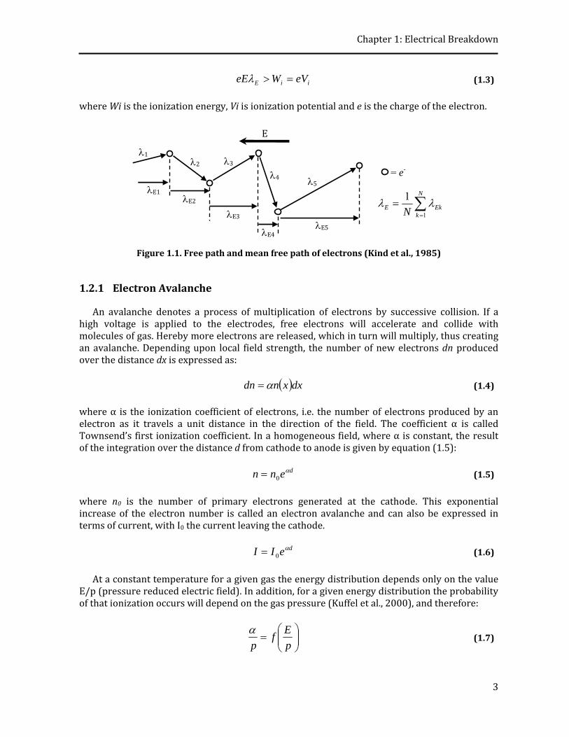
Ionization is possible if the amount of energy caused by collisions, electromagnetic radiation or secondary processes exceeds the ionization energy. The ionization condition can be expressed in terms of electric field strength E and mean ionizing free path λE, which is the average distance a particle traverses between collisions under the influence of electric field E (Nasser, 1971), as shown in Figure 1.1.
Chapter 1: Electrical Breakdown
3
iiE eVWeE (1.3)
where Wi is the ionization energy, Vi is ionization potential and e is the charge of the electron.
Figure 1.1. Free path and mean free path of electrons (Kind et al., 1985)
1.2.1 Electron Avalanche
An avalanche denotes a process of multiplication of electrons by successive collision. If a high voltage is applied to the electrodes, free electrons will accelerate and collide with molecules of gas. Hereby more electrons are released, which in turn will multiply, thus creating an avalanche. Depending upon local field strength, the number of new electrons dn produced over the distance dx is expressed as:
dxxndn (1.4)
where α is the ionization coefficient of electrons, i.e. the number of electrons produced by an electron as it travels a unit distance in the direction of the field. The coefficient α is called Townsend’s first ionization coefficient. In a homogeneous field, where α is constant, the result of the integration over the distance d from cathode to anode is given by equation (1.5):
denn 0 (1.5)
where n0 is the number of primary electrons generated at the cathode. This exponential increase of the electron number is called an electron avalanche and can also be expressed in terms of current, with I0 the current leaving the cathode.
deII 0 (1.6)
At a constant temperature for a given gas the energy distribution depends only on the value
E/p (pressure reduced electric field). In addition, for a given energy distribution the probability of that ionization occurs will depend on the gas pressure (Kuffel et al., 2000), and therefore:
p
Ef
p
(1.7)
2 3 4 5
1
E1 E2
E3
E4 E5
N
kEkE N 1
1
= e-
E

Chapter 1: Electrical Breakdown
4
The ionization coefficient α can be represented by an equation of the form (Kuffel et al., 2000):
pEBAep
//
(1.8)
where A and B remain relatively constants for a given gas over a range of fields and pressures. Equation (1.7) describes a dependence of α/p upon E/p, which has been confirmed experimentally within certain ranges of E/p. Therefore, for various gases the constants A and B have been experimentally determined. Some of these values for selected gases are listed in Table 1.1 (Nasser, 1971, Kind et al., 1985).
Table 1.1. Ionization Energies and Constants of Some Gases
Gas N2 Ar SF6 Air A (1/mm_kPa) 9.0 10.5 ‐ 11.2 B (V/mm_kPa) 256.5 135.0 ‐ 273.7 E/p range (V/mm_kPa) 75 – 450 75 – 450 ‐ 75 – 600 Ionization Energy Wi (eV) 15.6 15.9 15.9 ‐
1.2.2 Secondary Emission of Electrons
According to equation (1.6), for a given pressure a logarithmic graph of I vs. inter‐electrode distance should yield a straight line of slope α. However, Townsend observed that at higher voltages the current increased at a more rapid rate than given by equation (1.6). To explain that difference, Townsend postulated that a second mechanism must be affecting the current.
A number of secondary processes have been found, which play an important role in accounting for the exponential growth of the current (equation 1.6). The acceleration of positive ions in the electric field, due to the collision of electrons and molecules, leads to emission of secondary electrons from the cathode, as well as other processes, like the arrival of photons, neutral and metastable particles. Electrons produced by these processes are called secondary electrons.
The secondary ionization coefficient γ is defined as the number of secondary electrons produced per incident of positive ion, photon, excited or metastable particle. The total value of γ corresponds to the sum of all individual coefficients due to the secondary processes and is called “Townsend’s second ionization coefficient” (Naidu et al., 1996, Kuffel et al., 2000).
The Townsend model is based on the assumption that an avalanche begins near to the cathode due to n0 (Figure 1.2), and crossing the space d it generates 10 den ions. On striking
the cathode, these ions release 1γ 0 den secondary electrons through secondary emission
(Kind et al., 1985). Assuming n as the number of electrons reaching the anode per second, n0 as the number of
electrons emitted from cathode by u.v. illumination, n+ as the number of electrons released from cathode by positive ion bombardment, and γ as the number of electrons released from cathode per incident positive ion, then:
dennn
0 (1.9)
where:

Chapter 1: Electrical Breakdown
5
nnnn 0 (1.10)
Figure 1.2. Electron generation according to the Townsend mechanism (Kind et al., 1985)
Replacing equation (1.10) into equation (1.9) gives:
110
d
d
e
enn
(1.11)
or expressed in terms of current:
110
d
d
e
eII
(1.12)
Experimental values for γ can be determined from equation (1.12) for known values of E, p,
inter‐electrode distance d, and α. Values for γ are highly dependent on cathode surface. Low work function materials will produce greater emissions. The value of γ is small at low values of E/p and higher at greater values of E/p. This is to be expected, since at high values of E/p there are a greater number of positive ions and photons with energies high enough to eject electrons from the cathode.
1.2.3 From SelfSustained Discharge to Breakdown
The gases in which electron attachment occurs are electronegative gases. An attachment coefficient can be defined as the number of attachments per electron unit drift in the direction of the field. Under these conditions, the current growth in a uniform field is given by (1.13).
110
d
d
e
e
II
(1.13)
den 0 0n
10 den
1γ 0 den
+_
CATHODE
ANODE

Chapter 1: Electrical Breakdown
6
As the gap voltage increases, the electrode current at the anode increases according to equation (1.13). The current will increase until at some point the denominator of equation (1.13) becomes zero, then:
111
dd ee
(1.14)
where the ionization by electron collision is represented by the effective ionization coefficient . Under this condition equation (1.13) predicts that the electrode current becomes infinite. Equation (1.14) is known as Townsend’s breakdown criterion. This is defined as the transition from self‐sustained discharge to breakdown. Theoretically, the value of the current becomes infinite, but in practice it is limited by the external circuit and voltage drop across the spark which bridges the gap. A self‐sustaining discharge occurs when the number of ion pairs produced in the gap by the passage of one electron avalanche is large enough that the resulting positive ions bombarding the cathode are able to release one secondary electron and cause a repetition of the avalanche process. The secondary electron may also come from a photoemission process (Kuffel et al., 2000).
1.3 Streamer Mechanism
For uniform electric fields the growth of charge carriers in an avalanche is described as de . Raether, Loeb and Meek explained that this exponential growth of an avalanche cannot be increased at will since the avalanche becomes unstable at a critical length (Kind et al., 1985). This growth is valid only if the electric field produced by space charges can be neglected compared to the original uniform field E0 (Kuffel et al., 2000). Figure 1.3 shows the electric field around an avalanche as it progresses along the gap and the resulting modification to the original field E0.
Figure 1.3. Representation of field distortion in a gap caused by space charge of an electron avalanche (Kuffel et al., 2000)

Chapter 1: Electrical Breakdown
7
Consider a single electron starting at the cathode builds up an avalanche by ionization. Electrons have higher mobility and travel very fast compared to the positive ions in the avalanche. As electrons propagate towards the anode, the positive ions are almost in their original positions and form positive space charges at the anode (Naidu et al., 1996). The field is enhanced in front of the head of the avalanche (space charge at the head of the avalanche is assumed as a spherical volume) with field lines from the anode terminating at the head.
The Townsend theory accounts for the dependence of the breakdown voltage on gas density and electrode spacing. However, there are experimental results which appear to be incompatible with the Townsend mechanism (Kuffel et al., 2000). According to Townsend mechanism, the minimum formative time lag of the spark should be equal to the transit time of electrons. However, time lags much shorter than the transit time have been found in lab. In spark‐gaps, for example at atmospheric pressure with inter‐electrode distance around 10 mm, time lags were too short to have involved a series of successive avalanches produced by ions impinging on the cathode. The breakdown voltage in this case is independent of the cathode material, which is an evidence of qualitative difference from the Townsend breakdown. The mechanism of the electrical breakdown in this case is based on the streamer mechanism.
Raether observed that the local field distortion in Figure 1.3 becomes noticeable with a carrier number n > 106, but if the carrier number in the avalanche reaches n = 108 the space charge field becomes of the same magnitude as the applied field and may lead to the initiation of a streamer. Then: 2018108
0 cx xen c where xc is the length of the avalanche path in
the field direction when it reaches the critical size. As long as the net charge is insufficient to distort the field appreciably, the avalanche moves
with the electron drift velocity. When the electron avalanche head grows to a size such that the space charge distribution due to ions and electrons shield itself from the applied field, the propagation and growth of the avalanche change clearly, and the streamer phase follows. The necessary conditions for streamer propagation are: sufficient high energy photons must be created in the avalanche, the photons must be absorbed to produce sufficient electrons at the tip and the space charge field at the back of the avalanche tip shall be sufficient enough to produce the secondary avalanche in the enhanced field.
Figure 1.4. Representation of the development of the streamer. a. Negative streamer. b. Positive streamer (Naidu et al., 1996)
Loeb and Meek proposed the streamer theory of the spark for the positive streamer (Figure
1.4a) and independently Raether proposed the streamer theory for the negative streamer
ab

Chapter 1: Electrical Breakdown
8
(Figure 1.4b). At stage A in Figure 1.4b, the avalanche has crossed the gap. At stage B, the streamer has crossed half the gap length and at stage C the gap has been bridged by a conducting channel (Naidu et al., 1996). The channel is caused by a combination of photo‐ionization and collision ionization. Hence, secondary emission at the electrodes, as predicated by Townsend, is not essential.
Based on the experimental observations and some simple assumptions Raether developed an empirical expression for the streamer breakdown criterion:
E
Exx r
cc lnln7.17 (1.15)
where Er is the space charge field strength in radial direction at the head of avalanche as shown in Figure 1.5 and E is the externally applied field strength.
Figure 1.5. Space charge field (Er) around the avalanche head (Kuffel et al., 2000) Therefore, the resultant field strength in front of the avalanche is (E+Er). The condition for
the transition from avalanche to streamer supposes that space charge field Er approaches the externally applied field E, and hence the breakdown criterion is described as:
cc xx ln7.17 (1.16)
To obtain the minimum breakdown value for a uniform field gap by streamer mechanism is assumed that the transition from avalanche to streamer occurs when the avalanche has just crossed the gap. Then equation (1.16) takes the form (Kuffel et al., 2000):
dd ln7.17 (1.17)
The condition xc = d gives the smallest value of α to produce streamer breakdown. 1.4 Breakdown Voltage
1.4.1 Paschen’s Law
Since α/p is a unique function of E/p, and further, if one assumes that γ/p is also a function of E/p, Townsend’s breakdown criterion can also be expressed in terms of electric field or

Chapter 1: Electrical Breakdown
9
voltage. Consider a homogeneous field where E is constant (E = V/d). Expressing Townsend’s first ionization coefficient α (equation (1.8)) in terms of breakdown voltage (Vb) gives:
bVBpdpEB ApeApe /// (1.18)
Also, Townsend’s breakdown criterion, gives:
1
1ln
1
d (1.19)
Hence:
bVBpdAped
/11ln1
(1.20)
Solving for Vb:
11ln
lnApd
BpdVb
(1.21)
Equation (1.21) is called Paschen’s law and expresses breakdown voltage as a function of
pressure and inter‐electrode distance, Vb = f(pd) (Heylen, 2006). Figure 1.6 shows the measured Paschen curve for air at atmospheric conditions, in comparison with a theoretical curve derived from equation (1.21), using the parameters listed in Table 1.1 with 1 bar = 100 kPa.
Figure 1.6. Measured and calculated Paschen curves for atmospheric air (Bluhm, 2006)
Chapter 1: Electrical Breakdown
10
1.4.2 Breakdown in SF6
Based on equation (1.21), Vb should go to infinity at a certain value of pd, because it becomes impossible to create electron avalanches below this value. However, it does not happen, because at very high electric fields electron emission from the cathode occurs (Bluhm, 2006).
SF6 is mainly used as a gaseous dielectric medium in the electric power system. Pressurized SF6 has notably higher dielectric strength compared to air and thus enables significant reductions in electrical equipment size. However, SF6 can only be pressurized to 2000 kPa before it turns into liquid at room temperature (Kind et al., 1985). SF6 is part of the group of electronegative gases, which are characterized by the ability to attach electrons to the molecule. To describe the breakdown properties of this gas, the attachment coefficient must be considered. For SF6 most of the experimentally determined values for p/ fit well into a linear function of E/p.
0p
E
p
Ek
p
(1.22)
where k is an empirical constant equal to 27.7 [kV]‐1 and (E/p)0 = 88.4 [V/mm_kPa]. Experiments show that equation (1.22) is valid in the range 75 < E/p < 200 [V/mm_kPa] (Kuffel et al., 2000, Bluhm, 2006). Equation (1.22) in combination with the breakdown criterion in equation (1.19) is used for the calculation of breakdown field strength in SF6 for uniform or quasi‐uniform field.
pdk
K
p
E
p
Eb
0
(1.23)
Using K = 18 and the values of k and (E/p)0 described before, the following expression is obtained for the breakdown voltage in SF6 (Bluhm, 2006):
pdVb 4.88500 V (1.24)
where p is the pressure in [kPa] and d the inter‐electrode distance in [mm]. Equation (1.24) is valid for the range of values 40 < pd < 3000 [mm_kPa]. At higher values of pd the measured values of Vb are lower than predicted by equation (1.24). 1.5 SelfBreakdown SparkGaps
The understanding of the electrical breakdown in gases developed in the previous section is applied in the study of self‐breakdown spark‐gap, which is a configuration of two electrodes separated by an insulating gas medium. The spark‐gap changes from an insulating state to the conductive state if the voltage across the gap is increased above its self‐breakdown voltage.

Chapter 1: Electrical Breakdown
11
1.5.1 Arc Discharge
There are three typical features of arcs not found in other electric discharges: low cathode fall, relative high current density and high luminosity. Low cathode fall results from cathode emission mechanisms are capable of supplying a greater electron current from the cathode. The arc discharge is characterized by large currents (1–105 A). Arc cathodes receive a large amount of energy from the current and reach a high temperature, either over the entire cathode area or just locally, usually for short time intervals. The luminosity of the arc column is very high compared to other discharge modes and it has many applications in the illumination field.
The dominating process responsible for ionization in the arc channel is due to electron collision. In the case of high‐pressure arcs, the field strength in the arc channel is by far insufficient for an electron to accumulate enough kinetic energy over a mean free path to make an ionizing collision. In this condition, it is assumed that the electron travels in the field direction, accumulating the maximum possible energy from the electric field. Charge carrier production in this situation must be achieved by thermal ionization rather than field ionization. 1.5.2 Fundamentals of a Closing Switch
In the case of closing switches the switching process is associated with a voltage breakdown across an initially insulating gas. In this sense, there are two options: the breakdown occurs automatically as result of an overvoltage (self‐breakdown) or it is initiated by an external source (trigger). Several closing switches are available that operate in different pressure ranges. Figure 1.7 shows the range of gas pressures and operating voltages for some gas‐filled switches (Bluhm, 2006).
Figure 1.7. Range of pressures and operating voltages for some closing switches compared with the Paschen curve obtained for air for interelectrode distance of 3 mm (Bluhm, 2006)
In this thesis the range of pressures is located in the right side of the Paschen curve, the
region of high pressure spark‐gaps. The operating characteristics such as voltage and current
Chapter 1: Electrical Breakdown
12
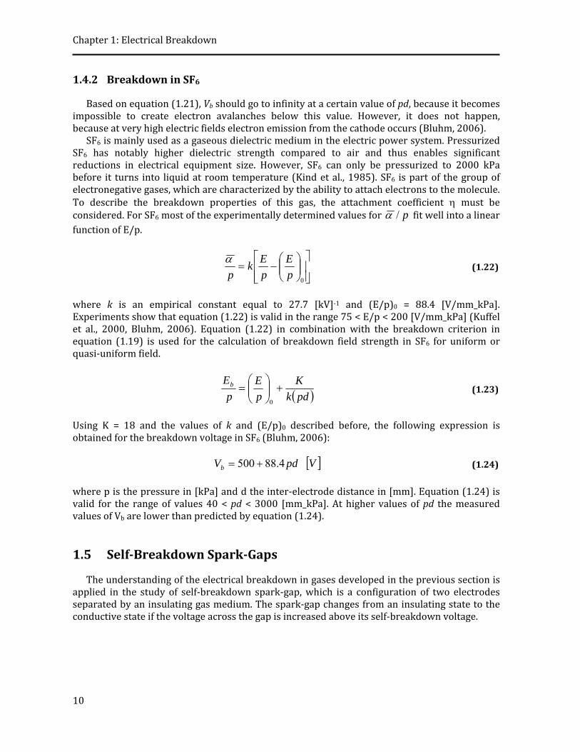
relationships related to a closing switch are shown in Figure 1.8. The operation of the switch can be divided into three phases:
Phase I (commutation phase): Transition from a high to a low switch impedance Phase II (stationary phase): Constant conductivity of the switch Phase III (recovery phase): restoration of the previous electric strength
Figure 1.8. Voltage, current and power loss in a sparkgap closing switch (Bluhm, 2006)
The efficient operation of the closing switch requires a gaseous medium with a large
breakdown voltage Vb, an extremely low conduction voltage Vc, and a short switching time ts. The voltage Vc across the two electrodes during the stationary phase is much lower than Vb depending on the degree of ionization. It is highly desirable that such switches close quickly and with a minimum energy loss. Christophorou et al. (1987) propose an efficiency parameter (Eff) depending on Vb and Vc.
2
1
b
cV
VEff (1.25)
Bluhm (2006) suggest that considerable energy consumption occurs only during the
commutation phase, and the energy loss (Ws) can be estimated assuming that voltage decay and current growth occur exactly at the same time:
56rmbsmb
s
tIVtIVW (1.26)
where Vb is the breakdown voltage, Im is the maximum current, ts is the switching time and tr is the pulse rise‐time (tr ≈ 0.8ts).
Vb
Vc

Chapter 1: Electrical Breakdown
13
The recovery phase refers to the time for recovery of dielectric properties of the gas so that the voltage can be reapplied to it. The recovery voltage of spark‐gaps that are operated at the high pulse repetition frequency (PRF) is below the DC hold‐off voltage. Most spark‐gaps require recombination and attachment of electrons in the recovery phase. Only after a finite delay, the recovery phase will progress and the voltage can be restored. This leads to the recovery characteristics that limit the PRF of switch operation.
In many cases, recombination and attachment may occur rapidly but the gas is then left in a highly heated state. Therefore, low gas density regions may persist. It means the mean free path of stray charges is much higher and reapplication of voltage may initiate an avalanche. Thus, the gas should not only be de‐ionized but also be cooled and homogenized to allow voltage recovery. This is the primary reason why gas flow is employed in many situations. At very high pressures, the recovery processes are such that the recovery time may decrease significantly, in part because of the intense cooling of the arc plasma.
1.5.3 Risetime Limit
Prior the breakdown, a spark‐gap is a capacitor, which does not necessarily charge fully before breakdown occurs. The spark‐gap cannot close in less time than the transit time of the electromagnetic wave through the gap. To examine the propagation time in the spark‐gap, Lehr et al. (1997) suggest that the transit time of an electromagnetic pulse through a spark‐gap filled with insulating media, electric permittivity , and magnetic permeability , is:
rpt
pd (1.27)
where p is the gas pressure, d the inter‐electrode distance and tr the rise‐time. For a spark‐gap inserted into a coaxial transmission line, the rise‐time is determined not only by the switch closure but also by the re‐establishment of the propagating electric field in the inter‐radial distance. The achievable rise‐time is longer, since the electromagnetic wave must be re‐established between the inner and outer conductors. Thus, equation (1.27) is modified given the minimum rise‐time achievable:
rdtr (1.28)
where r is the difference between the outer and inner radii of the coaxial transmission line. In practice, for most systems r is made large to ensure voltage hold‐off in the coaxial line. As the breakdown voltage is inversely proportional to both the inner radius and the logarithm of the radius ratio, for ultra‐fast switching the inner conductor must be as thin as possible. 1.5.4 Models for Resistive Phase Time
The switching time (ts) is the time a spark‐gap takes to pass from a non‐conductive to a conductive state, and it is described as the sum of the three phases: tsd, tsf and R, as shown in Figure 1.9, where tc is the time required to raise the gap voltage to the self‐breakdown voltage Vb, tsd is the statistical delay time until an electron is able to create an avalanche, tsf is the time between the avalanche formation and the onset of the breakdown (in this time the critical charge density is reached), and R is the time required for the channel heating. During this time

Chapter 1: Electrical Breakdown
14
the arc‐resistance changes from several tens of M to some m and therefore, it is also known as the resistive phase of the discharge channel. This phase decides the time dependent conductivity of the discharge channel and hence influences the rise‐time of the output pulse (Schaefer et al., 1990, Bluhm, 2006). In this thesis, breakdown is produced by slowly rising DC voltages and therefore only R plays an important role in the breakdown process.
Figure 1.9. Schematic of breakdown characteristic time (Schaefer et al., 1990) The understanding of the time dependent resistive phase of the discharge channel is
fundamental in the development of fast closing switches for use in pulsed power systems. An important factor in closing switches is the dissipation of energy during the closure phase, which is determined by the resistive phase as described by equation (1.26). Therefore, spark‐gaps that maintain a short resistive‐phase time are desirable.
Several authors have developed equations for calculating the resistive phase time in various gases, which depends on the electric field at breakdown, the pressure or gas density and the impedance of the circuit driving the conducting channel. The resistive phase time is strongly dependent on the electric field value, and for a given electric field, resistive phase time decreases with gas density as given by the equation proposed by Martin (1965):
2
1
031
03
4
0
88
ZER
ns (1.29)
where and 0 are the density of the gas in the gap and the density of the air at S.T.P., respectively, Z0 is the impedance of the circuit driving the conducting channel, and E0 is the electric field along the channel in [kV/mm]. Equation (1.29) has been shown to produce excessively high resistive times, which is corroborated in this thesis. Martin’s equation gives similar results as Sorensen and Ristic equation for nitrogen (Sorensen et al., 1977), which depends on the pressure p instead of the density of the gas:
21
31
00
44p
ZER
ns (1.30)
VVOV
Vb
tsd tsf R tcts

Chapter 1: Electrical Breakdown
15
Both equations are applied in the same field regions (E0 ≈ 8 kV/mm). For electric field intensities in the range of 22 to 60 kV/mm, Sorensen and Ristic proposed the equation (1.31) for helium.
21
31
02
1
0
4.6p
ZER
ns (1.31)
Based on laboratory test results in hydrogen, Pécastaing et al. (2001) suggested that the
influence of the gap is not very great and resistive time is dependent solely on the field strength, as described by equation (1.32).
807.00
023.2
ER ns (1.32)
1.5.5 Models for ArcResistance
The arc‐channel‐resistance is a function of the temporal development of some physical processes including the electron kinetic processes. Several experimental and theoretical analyses of the discharge channel time dependent resistance have been made to describe the transition from a streamer channel to a low resistance channel (Bluhm, 2006). Some of the most important discharge channel time dependent models are: Kushner (1985), Toepler, Rompe and Weizel, Vlastos (1972), Sorensen and Ristic (1977) and Braginskii (1958).
The most widely used arc‐resistance model is the empirical model proposed by Toepler in 1906 (Montaño et al., 2006, Bluhm, 2006). Assuming that a weakly conducting column exists and its conductivity increased by multiples ionizations, and that the mean current density is a function of the electron mobility and the mean electric field in the spark‐gap, an equation for the spark‐resistance was obtained. In that model, the resistance is inversely proportional to the charge that flows through the channel. As the current flows through the column, it tends to heat and therefore to expand. However, this phenomenon was not taken into account in this model. Bluhm (2006) suggests that Toepler’s model is valid only for a limited period of time after the channel formation, which is approximately 10 ns for a gas at atmospheric pressure.
An improvement of Toepler’s model was proposed later by Rompe and Weizel in 1944 (Vlastos, 1972, Montaño et al., 2006, Bluhm, 2006). In this model, the energy balance of the discharge channel was included, but similar to the Toepler’s work, they neglected the channel expansion. Finally, Rompe and Weizel found a similar expression for the discharge channel‐resistance.
Braginskii (1958) showed that the resistive collapse of the electric discharge is governed by the thermal expansion of the plasma channel. Braginskii’s theory assumes a cylindrical channel in which the gas inertia is neglected and the pressure is constant all the way through. The length of the transition region between the channel and the ambient gas is negligible and the temperature and ionization drop sharply to the ambient conditions. The transition region expands rapidly creating a shock wave. From energy conservation, Braginskii derived his known equation for the discharge channel radius, which assumes a specific channel conductivity independent of time. An arc‐resistance model was also obtained using both, the Braginskii’s channel radius model and the cylindrical conductor resistance equation.
Rompe and Weizel’s model assumes that the arc‐resistance can be obtained from its energy equation. In that case, only the energy required to change the internal energy of the plasma was

Chapter 1: Electrical Breakdown
16
considered. Vlastos (1972) derived a relation for the temporal variation of the arc‐resistance. He assumed that the plasma conductivity in the spark‐gap stayed at a quasi‐stationary state at the moment of the channel formation and suggested that additional changes in the arc‐resistance were due to the channel expansion. Therefore, assuming that the channel plasma is single and fully ionized, and that the electron and ion temperatures of the ionized channel gas are equal, an expression for the arc‐resistance was obtained.
In 1977 Sorensen and Ristic (1977) presented their work, in which the spark‐gap was located between the center conductors of a coaxial line. The coaxial line was ended in short‐circuit just after the spark‐gap. Voltage pulses with a width of 2 µs were applied. To measure the generated pulses, a magnetic field sensor was located before the switch. Nitrogen and Helium were used under pressures between 200 and 600 kPa, with an inter‐electrode distance between 50 and 500 µm. The transmitted current and the reflected current were measured and the temporal variation of the arc‐resistance was obtained.
Kushner (1985) worked with laser‐triggered spark‐gaps at pressures between 25 and 200 kPa, and with a fixed inter‐electrode distance of 12 mm for SF6 and some gas mixtures. The spark‐gap current and voltage were measured with a shunt resistance and a capacitive voltage divider built into the discharge chamber. The discharge channel diameter was also registered, and the inductance was calculated. After that, the voltage drop in the arc‐inductance was discounted to the measured voltage signal leaving only the voltage drop in the arc‐resistance. The temporal behavior of the arc‐resistance was calculated as a relation between the resistive voltage drop and the current through the spark‐gap.
Several studies have been carried out using the arc‐resistance equations presented in Table 1.2 (Cary et al., 1979, Akiyama et al., 1988, Gratton et al., 1988, Engel et al., 1989, Istenic et al., 2005, Montaño et al., 2006). Unipolar, critically damped and over‐damped pulsed discharges with rise‐times of 700 ns were investigated by Akiyama et al. (1988). From a circuit equation approximation and using the measured values of current and breakdown voltage, the temporal dependence of the arc‐resistance was calculated. The gap distance and the air pressure were changed from 1 to 16 mm and from 40 to 130 kPa. As a conclusion, the arc‐resistance of the initial phase calculated with the Rompe and Weizel’s model was in good agreement with the experimental results. Also, the authors suggested the need to do new experiments changing some parameters, such as the load, types of gases, pressures and electrode materials.
The predictions of some of the models described in Table 1.2 (Toepler, Rompe and Weizel, Vlastos and Kushner) were tested against the experimental data of Akiyama by Engel et al. (1989). In this case, Kushner’s model fitted best the experimental results throughout the pulse time duration (~4 µs), and models of Rompe and Weizel and Vlastos had a good agreement with the experimental results during the initial state of the discharge channel. However, that study was based on the results obtained for a pulse having time duration in the range of µs. Therefore, it is of interest to study the behavior of these models for shorter pulses.
An experimental work was developed by Cary et al. (1979), in which the arc‐resistance was estimated for the first 1.5 ns of breakdown for four gases (nitrogen, argon, hydrogen and a mixture of argon and hydrogen), three gas pressures (100, 270 and 440 kPa) and two gap distances (25.4 and 76.2 µm). As a result, important differences were found when measurements in nitrogen were compared with Sorensen and Ristic data.
In (Montaño et al., 2006) the authors presented the experimental results of laboratory tests conducted to calculate the temporal variation of the arc‐resistance in two series of experiments. In the first one, 10/350 µs current impulses between 35 and 48 kA were applied to a 10 mm gap. In the second one, a Marx generator was used to apply 300 kV and 1 MV lightning voltage impulses to a 128 mm gap. Experimental results were compared with some of the models in

Chapter 1: Electrical Breakdown
17
Table 1.2. The best approximation of the calculated temporal variation of the arc‐resistance was obtained with the equation of Kushner. However, the differences between measured and predicted arc‐resistances by the most accepted models are large enough to warrant further development of theoretical and empirical models.
Table 1.2, adapted from (Engel et al., 1989, Montaño et al., 2006) shows a summary of the main arc‐resistance equations.
Table 1.2. ArcResistance Models (Engel et al., 1989, Montaño et al., 2006)
Researcher Equation [] Parameters Test conditions
Toepler [1906]
0.
.
dti
dk
k: model constant d: inter‐electrode distance [m] i: current in the channel [A]
d = 9 – 17,5 [mm] p = 100 [kPa] In air
Rompe and Weizel [1944]
0
2
0
2 dtip
k
d k: model constant d: inter‐electrode distance [m] p0: Initial pressure in the gas [kPa] i: current in the channel [A]
d 35 [mm] p0 = 100 – 600 [kPa] In air Unipolar pulse, 50 [ns]
Braginskii [1958]
0
322. dtik
d k: model constant d: inter‐electrode distance [m] : channel conductivity [.m] i: current in the channel [A]
Empirical model
Vlastos [1972] 5
3
0
2
52
..
dti
rdk
k: model constant d: inter‐electrode distance [m] r: channel radius [m] i: current in the channel [A]
d = 130 [mm] Exploding wire
Sorensen and Ristic [1977]
3
31
0
21
.
tZE
pk
k: model constant p: Pressure in the gas [kPa] E: Electric field [kV/m] Z0: TL impedance []
p = 200 – 600 [kPa] d = 50 – 500 [µm] Ni, He Unipolar pulse, 100 [ns]
Kushner [1985]
51
62
30.
iA
pdk
k: model constant d: inter‐electrode distance [m] p0: Initial pressure in the gas [kPa] A: Channel cross‐section area [m2] i: current in the channel [A]
j = 2x10⁴ [MA/m] d = 12 [mm] p0 50 [kPa] SF6, H2, N2, CH4, Xe Unipolar pulse, 100 [ns]

Chapter 1: Electrical Breakdown
18

2 Chapter 2: Experimental Setup
The switching element is the most important component in a pulsed power system. The fast rise‐time pulse that this element produces is a fundamental parameter, since it determines the high frequency components for an Ultra Wide Band (UWB) system. In this sense, for a gas switch, making the electric field in the gap between the two electrodes as high as possible is important in order to obtain signals with rise‐times in the order of hundreds of picoseconds or shorter (Cary et al., 1979, Martin, 1992, Pommerenke, 1995, Dick et al., 2000, Carboni et al., 2002, Nunnally, 2005, Heeren et al., 2007, Wang et al., 2007).
In recent years, researchers have drawn their attention to the range of nanoseconds to sub‐nanoseconds due to commercial and military potential applications. Such recent interest is also encouraged by the technological advances in diagnostic systems and measuring devices, which permit recording data at pico‐second timescales (Dick et al., 2002, Carboni et al., 2002, Bluhm, 2006).
This chapter includes the description of the design, simulation and construction of a pulse generator constructed to study the gas discharge phenomenon within sub‐millimeter spark‐gaps and also to be part of a radiator system for electromagnetic compatibility tests. This chapter presents the electrical, physical and mechanical characteristics of the pulse generator obtained in the design process and supported in the simulations conducted using both the Electromagnetic Transient Program EMTP‐ATP1 and the Finite Element Program COMSOL2.
Some of the typical approaches for fast breakdown in gases have been developed from the Fletcher’s work (Fletcher, 1949), where it was proposed the use of transmission lines consisting of coaxial cables with a small spark‐gap switch as part of the transmission line system and a step pulse like a source to obtain gas breakdowns on nanosecond timescales. In (Cary et al., 1979, Greason, 1999, Dick et al., 2000, Carboni et al., 2002, Wang et al., 2007, Heeren et al., 2007, Yin et al., 2008) a low inductive resistor with a value equal to the characteristic impedance of the transmission lines was used as a load.
The measurement of signal parameters such as rise‐time, signal peak and pulse duration is another important aspect of pulsed power technology (Baum et al., 1978, Baum, 1981, Bluhm, 2006). The basic electrical quantities are always the electric and magnetic fields, from which pulse current and voltage must be derived. Likewise, an appropriate sensor has to be placed so as not perturb the field to be measured (Bluhm, 2006). In this chapter the measuring system is described and the location of the sensors in the generator is analyzed from transmission line simulations carried out in the EMTP‐ATP program. With the development of this chapter, the
1 http://www.emtp.org/ 2 http://www.comsol.com

Chapter 2: Experimental Set‐up
20
first specific objective of this thesis “To design and construct a sparkgap with a characterized current and voltage measuring system” is reached.
2.1 Pulse Generator
Each part of the generation system was taken into account in the design process. These parts are: High Voltage source (H.V.), Pulse Forming Line (PFL), Spark‐Gap, Transmission Line (TL) and Load (Figure 2.1).
Figure 2.1. Schematic representation of a pulse generator
Before describing each part of the generator, it is necessary to define the signal waveform to produce. In general, a square pulse is expected when a pulse generator is designed. However, the processes that occur during the electric discharge in the gas and the generator topology cause the signal to rise in a finite time (rise‐time). Such rise‐time must be adjusted depending on the high frequency cut‐off (fH), which determines the bandwidth of the signal. It is common to consider continuous wave (CW) electromagnetic signals in the frequency domain, and electromagnetic pulses (EMP) in the time domain. However, a continuous wave, as a sine wave, has a characteristic rise‐time and a pulse signal has an equivalent frequency, and then both forms can be analyzed in any domain. Based on that and using the procedure described in (Edgel, 1990‐1), the minimum rise‐time (tr) can be determined as a function of the high frequency (fH) required.
Hr f
t35.0
s (2.1)
Based on the requirements of the Cattleya Project, a high frequency cut‐off equal to 1 – 1.4
GHz was defined and therefore the rise‐time of the produced signals must be less or equal to 250 – 350 ps. Additionally, the energy per pulse to produce an effect in the specific underground target was defined to be Wpp = 10 mJ.
2.1.1 High Voltage Source
The D.C. voltage source used in laboratory tests was a Hipotronics high voltage source, 800 PL series, with a maximum negative voltage of 80 kV and 10 mA as the maximum D.C. current. For a maximum current of 10 mA through the source, a 8 M current limiting resistor like a minimum value should be used at the input of the generator. However, a 50 M resistor is available in laboratory stock and then it was used as a part of the pulse generator. Under this condition, the maximum D.C. current is 1.6 mA.
The use of this 50 M resistor does not affect the generated waveforms; the only change is in the pulse repetition frequency, which depends on the value of this resistance (equation (2.20)).

Chapter 2: Experimental Set‐up
21
2.1.2 Pulse Forming Line PFL
The transmission line characteristic impedance (Zc), the energy per pulse (Wpp) and the maximum voltage (Vm) were the design parameters of the Pulse Forming Line (PFL). From these parameters, it is possible to obtain features such as the transmission line capacitance (C), inductance (L), length (l), inner conductor radius (a) and outer cylinder radius (b).
As design criteria, the maximum voltage in the PFL is 40 kV, air at atmospheric conditions is used as dielectric in the coaxial system, and the transmission line characteristic impedance is 100 (see section 2.1.5). The energy in the PFL is:
2
2
1CC CVW (2.2)
Assuming that all energy stored in the PFL is transmitted through the transmission lines without losses, Vc = Vm and Wc = Wpp, and then:
122
2
m
pp
V
WC pF (2.3)
Using the typical equations of a coaxial transmission line, the parameters of the PFL were
found, namely Zc = 100 , C = 12 pF, L = 120 nH and l = 0.36 m. Additionally, based on the electrical breakdown theory the inner conductor radius (a) and outer cylinder radius (b) were calculated to withstand a D.C. voltage of 40 kV, and then a = 9 mm, b = 47.75 mm. Full Width at Half Maximum (FWHM)
Assuming that the generated pulse is square, the Full Width at Half Maximum (FWHM) corresponds to the same pulse length.
Figure 2.2. Ideal output voltage
Under this condition, the energy through the load (R) is:
PA
L TR
VW .
2
(2.4)
where VA is the voltage across the load and Tp is the pulse length. Assuming that all energy stored in the PFL (equation (2.2)) is transferred to the load and also knowing that VA = VC/2 (Martin et al., 1996), Tp can be expressed as a function of R and C as follows:

Chapter 2: Experimental Set‐up
22
PC
C TR
VCV .
42
1 22 (2.5)
Then:
4.22 RCFWHMTP ns (2.6)
Maximum DC Voltage
In this section, the maximum DC voltage (Vm) in the PFL before the breakdown is estimated. This calculation is carried out using the empirical relation developed by Peek for a coaxial cylindrical geometry (Kuffel et al., 2000):
DEC
05.315.3 m
MV (2.7)
where EC is the corona onset electric field, D = b‐a = 38.8 mm is the distance between inner and outer cylinders, and is the relative air density given by:
T
p
2739.2 (2.8)
where T and p are the ambient temperature in [ºC] and the pressure in [kPa], respectively. For the average ambient conditions of Bogotá, p = 76 kPa and T = 15 ºC. Then = 0.77. Therefore, under these conditions the electric field necessary for corona inception is EC = 2.8 MV/m. On the other hand, the electric field Er in the space between cylinders at radial distance r is given by:
a
br
VEr
ln.
(2.9)
where V is the applied voltage in [kV], r is the radial distance in [mm] and b and a are as defined previously. As the corona onset occurs when the voltage stress at the inner conductor reaches electric field required to begin the breakdown process (Ec), it is possible to rewrite the equation (2.9) as:
42ln
a
baEV CB kV (2.10)
The breakdown voltage of the PFL is 42 kV, thus it is greater than the maximum voltage
condition for this geometry (40 kV). Table 2.1 shows the geometrical and electrical parameters of the Pulse Forming Line.

Chapter 2: Experimental Set‐up
23
Table 2.1. Design parameters of the PFL
Parameter Symbol Value Unit Characteristic Impedance Zc 100 Ω Capacitance per unit of length C’ 33.7 pF/m Inductance per unit of length L’ 337 nH/m Length l 0.36 m Inner conductor radio a 9 mm Outer conductor radio b 47.8 mm Full Width at Half Maximum FWHM 2.4 ns Relative dielectric constant r 1 ‐ Relative magnetic constant µr 1 ‐ Maximum DC voltage Vm 40 kV
2.1.3 The SparkGap SG
The main parameters that define the spark‐gap characteristics are: the material, form and size of the electrodes, the gas, the pressure and the inter‐electrode distance.
The Electrodes
In this work, a uniform electric field between the two electrodes is required. Ideal flat plates with reasonable dimensions are difficult to construct. Finite sized plates produce a uniform field at the middle of the plate, but the high field at the edges creates a problem. Additionally, the discharges should take place only within the uniform electric field region and not in other part where the field is non‐uniform.
For an arbitrary shape electrode, determining the electric field, particularly in a dynamic case, is quite difficult, and would normally be necessary to do it by numerical techniques. However, for some cases an analytical expression for the field can be developed. The case of finite flat plates is one of them and its expression was developed by Maxwell and further extended by Rogowski (Prowse et al., 1958, Pearson et al., 1969, Giao, 1980). In the case of Rogowski profile, using the Maxwell’s transformation the analytic function is:
wewd
z 1
(2.11)
where d is the inter‐electrode distance, and z and w are the complex planes defined as:
jyxz (2.12)
jw (2.13)
where (x,y) is the 2D axial‐symmetric coordinate system where the profile is created and y is the axis of symmetry, and (,) is an auxiliary 2D rectangular coordinate system.
The Rogowski profile calculates the edges for two semi‐infinite electrodes with a mid plane of infinite extent between them and a distance between an electrode and the mid plane of d/2. The plates are located at the coordinates =‐, =, >0. The equipotential lines within the plates have the form =const and the electric field lines are =const (Figure 2.3). This means

Chapter 2: Experimental Set‐up
24
that the equipotential lines and the electric field lines coincide with the coordinates and , respectively. The values of x and y are given by:
cos1 ed
x (2.14)
sined
y (2.15)
Figure 2.3. Electric field lines (=const) and Electric potential lines (=const) in a semiinfinitelength parallel plate array in w plane
Figure 2.4 shows different Rogowski profiles solving the equations (2.14) and (2.15) for an inter‐electrode distance d = 1 [arbitrary units].
Figure 2.4. Rogoswki profiles from Maxwell’s transformation for different (, ) values. Blue lines: constant lines. Red lines: constant lines
Rogowski found that the electric field gradient between the electrodes is greater than the
gradient outside the plane section for ≤ /2. In the limit ( = /2), equations (2.14) and (2.15) reduce to:
= /2
=
= ‐

Chapter 2: Experimental Set‐up
25
1 d
x (2.16)
ed
y (2.17)
Figure 2.4 shows the curve for = /2, which was finally selected, and the curves for = ‐,
0 and . Note that the electric field lines () maintain a constant behavior in the plateau region of = /2. The electrodes were designed for a fixed inter‐electrode distance; however, the generator was designed to work in an inter‐electrode distance between 0.3 mm and 1 mm. Electrostatic simulations for different inter‐electrode distances were performed using the Finite Element Program COMSOL3 and so the influence of the electrodes in the electric field distribution was evaluated. The equipotential lines and the normal electric field are plotted in Figure 2.5 and Figure 2.6, respectively.
Figure 2.5. Equipotential lines from COMSOL simulation for d = 0.5 mm
Figure 2.6. Electric field lines from COMSOL simulation for d = 0.5 mm
3 http://www.comsol.com

Chapter 2: Experimental Set‐up
26
It can be seen from Figure 2.5 that the equipotential lines follow the shape of the electrodes. It can also be seen from Figure 2.6 that the electric field is uniform and maximum between the flat part of the electrodes.
Table 2.2 shows the background electric field (Eback) and the maximum electric field (Emax) for different inter‐electrode distances. Emax was calculated by using the COMSOL results for each inter‐electrode distance. The background electric field over the distance d between the two electrodes with voltage V = 1 V was calculated as Eback = V/d. Table 2.2. Enhancement Factor calculation for different interelectrode distances and 1 V applied
between the electrodes
d [mm] Eback [V/m] Emax [V/m] f 0.30 3333.33 3333.34 1.0000.50 2000.00 2000.08 1.0000.75 1333.33 1334.36 1.0011.00 1000.00 1005.53 1.005
The enhancement factor (f) also appears in Table 2.2, and it was calculated as:
backE
Ef max (2.18)
Results in Table 2.2 show that the electric field is not affected by the designed electrodes.
Figure 2.7a shows a 3‐D model of the electrode generated from the Rogowski profile in the software Autodesk Inventor4. Other details in this model are: the o‐ring place in the bottom side of the electrode, and the thread used to attach the electrodes to the transmission lines. Figure 2.7b shows a detail of the electrodes dimensions.
Figure 2.7. Electrode designed with Rogowski profile. a. 3D model. b. Electrode dimensions
Donaldson et al. (1983) concluded that the stainless‐steel 304 may be an economical replacement for Copper‐Tungsten composites as an electrode material due to its low erosion rates. Additionally, from the research group experience, it is possible to fabricate electrodes with a Rogowski profile using stainless‐steel with the required dimensions and low uncertainty
4 http://usa.autodesk.com/autodesk-inventor/
a b
Chapter 2: Experimental Set‐up
27
in the machining process. Based on that stainless‐steel 304 was selected as the material for the electrodes. The work function of this material is in the order of 4.4 [eV].
Pressurized Chamber
Due to the Cattleya project request5, it was decided to work in a range of pressures between 100 and 1000 kPa. Therefore, the pressurized chamber, which houses the electrodes and is the place where the electric discharge occurs, must withstand these pressure levels without suffering any deformation or leakages and without affecting the formation of the discharge and the propagation of the electromagnetic waves produced by the discharge. Figure 2.8 shows the model of the pressurized chamber designed in the software package Inventor.
Figure 2.8. Pressurized chamber designed in Inventor The material selected for this dielectric piece was Ultra‐High‐Molecular‐Weight Polyethylene
(UHMW‐PE), which has a dielectric constant r = 2.3. Complete information about the UHMW‐PE properties is presented in Appendix 1.
The main parts of the spark‐gap are shown in Figure 2.9. Two dielectric casings were designed and when these are joined together, the o‐rings in the casing ensure that there are not gas leakages. The gas inlets and the electrodes position within each casing are also shown in the figure.
2D axial‐symmetric simulations were performed using the Structural Mechanics module of COMSOL6 to determine if the walls of the pressurized chamber suffer any deformation due to the pressure contained within it. In the program, the profiles of the electrodes were approximated to flat electrodes made of stainless steel and the pressurized chamber geometry was drawn. A pressure (p) between 100 to 1200 kPa distributed to the walls and the surface of the electrodes was applied. The mechanical properties of the UHMW‐PE included in the
5 The Cattleya project objective is to radiate electromagnetic signals to a specific underground target 6 http://www.comsol.com

Chapter 2: Experimental Set‐up
28
simulation were: Young’s module = 830 MPa, Poisson’s ratio = 0.46 and density = 930 kg/m3. The effect of the ambient temperature was not included in the simulation.
Figure 2.9. Details of the sparkgap. Note the electrodes position, the electrodes and the gas inlet
and outlet Figure 2.10 shows a detail of the geometry and the boundaries used in the simulations,
where p0 = 74 kPa is the average atmospheric pressure in Bogotá.
Figure 2.10. Geometry and Boundary conditions of the simulation performed in COMSOL
Gas inlet
Pressurizedchamber
Gas outlet
Electrode
Electrode
PFL
TL
p
p
p0
p0
p0
UHMW‐PE
Electrode
Electrode
Inter‐electrodic gap
Axis of symmetry
r (mm)
z (mm)
19
45.25

Chapter 2: Experimental Set‐up
29
Figure 2.11 shows a detail of the simulation results when 1200 kPa were applied. The displacement of the upper and lower electrodes is 2.816 m and 2.492 m, respectively. Then, a maximum displacement of 5.31 m in the axial direction is observed, whereas the maximum variation in the radial direction is 1.3 m. On the other hand, the maximum electrostatic pressure produced by the high electric field between the electrodes is 210 kPa. With that pressure a maximum displacement less than 600 nm, in both radial and axial directions is observed.
Figure 2.11. Structural simulation of the pressurized chamber for p = 1200 kPa
Table 2.3 summarizes the results of the simulations for different pressures.
Table 2.3. Maximum displacement of the pressurized chamber walls in radial and axial axes
p (kPa) radial displacement (m) axial displacement (m) 174 ‐0.22 0.40 274 ‐0.33 0.88 374 ‐0.44 1.35 474 ‐0.54 1.83 574 ‐0.65 2.30 674 ‐0.76 2.77 774 ‐0.87 3.25 1000 ‐1.15 4.32 1200 ‐1.35 5.31
Based on COMSOL simulation results the maximum error in the inter‐electrode distance
introduced by the displacement of the pressurized chamber walls is around 1.7%. However, in
-0.595
-0.56
-0.565
-0.57
-0.575
-0.58
-0.585
-0.59
-0.595
-0.6 0 0.005 0.001 0.015 0.02
2.5 2 1.5 1 0.5 0 -0.5 -1 -1.5 -2
Max: 2.816
Min: -2.492
Surface: z-displacement [m]

Chapter 2: Experimental Set‐up
30
section 2.3 from laboratory results it is shown that the displacement is larger than the presented in Table 2.3.
2.1.4 The Transmission Line TL
The transmission line transfers the generated signal to the load. The TL length (lTL) should be at least the half of the total length of the transmitted signal so as to discriminate between the transmitted signal and the possible reflected signal measured by the D‐dot sensors (more information about them in section 2.3).
PW TcL (2.19)
where Lw is the length of the transmitted signal, c is the speed of light and Tp ≈ FWHM = 2.4 ns, and thus Lw = 0.70 m. Therefore, the transmission line length will be at least 0.35 m. Furthermore, the D‐dot should be located after the switch at the beginning of the TL, so that when the reflected signal reaches the sensor, the main part of the transmitted signal will have already passed it.
The other dimensions of the TL are the same that in the PFL. Furthermore, the same parameters defined by the PFL were used in the TL. 2.1.5 Load
Depending on the application, the load will have different mechanical, geometrical and electrical characteristics that will influence the behavior of other generator parts. For that reason, during the design process it was necessary to take into account all the system elements as a whole and not separately, since to make changes or adjustments to the existing geometry is difficult once the generator has been built.
In general, when the objective is to radiate electromagnetic pulses, the load will be an antenna, while a constant impedance load is normally used if the goal is to transmit conducted signals. The Cattleya Project objective is to radiate EM signals to a specific underground target. In that sense, some radiator systems have been studied using antennas with a real part of the input impedance of almost 100 (Vega, 2011). On the other hand, the objective of the present thesis is the generation of fast pulses and the analysis of the signals to understand the gas discharge behavior under these specific conditions. Based on those criteria, the use of resistive loads with a constant value is more appropriate.
Therefore, a cylindrical load with a resistive value of 100 has been selected. A coaxial design has the advantage that the current flowing through the resistor ideally does not produce electromagnetic fields outside of the space between the coaxial conductors, and as a result, the output signal does not contain inductive components. Assuming that energy per pulse is 10 mJ, and using the pulse duration calculated in the previous section (FWHM = 2.4 ns), the average power per pulse (Ppp) was calculated, finding an approximate value of 6.25 MW. Then, the 100 resistor must withstand a power of 6.3 MW during a few ns. Finally, the design parameters of the resistive load were:
R = 100 Wpp = 10 mJ Ppp = 4.17 MW @ FWHM = 2.4 ns

Chapter 2: Experimental Set‐up
31
Based on that information, four high power ‐ high voltage cement resistors of 25 in series connection were used as load. 2.2 Final Design
Figure 2.12 shows a schematic diagram of the designed coaxial pulse generator with the sizes of the used parts and materials according to the parameters described above. The spark‐gap is located into the pressurized chamber and the 100 transmission line ends at a 100 resistance (LOAD). All metallic parts were made of stainless steel and plastic components were made of UHMW‐PE.
Figure 2.12. Schematic diagram of the designed pulse generator. All dimensions in mm
The main parameters of the designed generator are summarized in Table 2.4.
Table 2.4. Design parameters of the pulse generator
Parameter Symbol Value Unit Maximum D.C. Voltage Vm 40 kV Characteristic impedance Z0 100 Maximum energy per pulse Wpp 10 mJ High frequency cut‐off fH 1 GHz Minimum rise‐time achievable tr 130 ps Full Width at Half maximum FWHM 2.4 ns Maximum Pulse Repetition Frequency PRF 10 kHz Inner conductor radio a 9 mm Outer conductor radio b 47.75 mm Total Length lT 1.14 m
360.00 592.00 142.4045.25
18.00 95.50Stainless steel
Stainless steel
UHMW‐PE
PFL TL LOAD
SPARK‐GAP

Chapter 2: Experimental Set‐up
32
where the minimum rise‐time achievable was calculated from equation (1.28) and the generator parameters, and the maximum pulse repetition frequency was calculated as follows.
Vega (2011) proposed a model to calculate the Pulse Repetition Frequency (PRF) as a function of the applied voltage (VDC), the spark‐gap breakdown voltage (Vb), the PFL capacitance (C) and the current limiting resistor (RS) connected between the high voltage source and the generator (equation (2.20)).
For SF6 at 174 kPa and an inter‐electrode distance d = 350 m, the breakdown voltage is Vb =
6 kV (from equation (1.24)). Moreover, RS = 50 M and C = 12 pF. Thus, for VDC = Vm = 40 kV the maximum expected PRF is around 10 kHz.
The constructed generator together with its main parts is shown in Figure 2.13. Note the manometers used to control the pressure in the spark‐gap volume and the transmission line. The 50 M current limiting resistor, the electrodes and the pressurized chamber are also shown in the Figure.
Figure 2.13. Constructed pulse generator and its main parts, including the transmission lines, the electrodes, the pressurized chamber, the 50 M limiting resistor and the 100 load
bDC
DCS VV
VCR
PRF
ln
1
(2.20)

Chapter 2: Experimental Set‐up
33
2.3 Measuring system
2.3.1 Diagnostic
Two electric field sensors FD‐5A (D‐dot) manufactured by Prodyntech Inc. were used to obtain the voltage drop in the spark‐gap (Figure 2.14).
Figure 2.14. Pictures of the electric field sensors (Ddot) The equivalent electric circuit and transfer function of such devices are presented in (Edgel,
1990‐2); based on such analysis, the output voltage (V) can be calculated as:
1
..
sCR
RsDsAsV
EE
EEQ (2.21)
where AEQ is the equivalent area of the sensor, D represents the electric displacement, CE and RE are the capacitance and output resistance of the sensor, respectively. The technical characteristics of the sensor provided by the manufacturer are as follows: RE = 50 , CE = 318.3 fF and AEQ = 14 m2. Finally, the relationship between the D‐dot sensor output voltage (V) and the voltage across the transmission lines (VAB) is:
dttVtVAB .1011.1 13 (2.22)
Figure 2.15. Pulse generator. Note the location of the Ddot sensors, one on the PFL before the sparkgap, and the other one on the TL after the sparkgap
Chapter 2: Experimental Set‐up
34
To calculate the voltage drop across the spark‐gap (VSG) it was necessary to measure the voltage in both, the Pulse Forming Line (V1) and the output Transmission Line (V2), as shown in Figure 2.15. A complete description about the operation mode of the sensors is presented in Appendix 2. Also the frequency response curve provided by the manufacturer is included in this appendix. In (Agilent, 2002, Agilent, 2012) relations to estimate the necessary oscilloscope bandwidth,
minimum rise‐time and minimum sample rate to make accurate measurements are proposed.
%3
%3
%3
4
64.0
92.1
BWSR
tT
fBW
rr
H
(2.23)
where BW3% and Tr3% are respectively the minimum oscilloscope bandwidth and the maximum oscilloscope rise‐time to measure the 10 – 90 % rise‐time (tr) with 3 % of error, SR is the minimum sample rate and fH is the high frequency cut‐off. Therefore for tr = 350 ps and fH = 1.4 GHz, an oscilloscope with a bandwidth of 2.7 GHz, 220 ps of rise‐time and 11 GSa/s of sample rate is required. Based on these conditions, measurements were conducted using an Agilent model 54855A oscilloscope with an analog bandwidth of 6 GHz, which provides raw samples every 50 ps (20 GSa/s), and a rise‐time of 70 ps. The oscilloscope was connected to a PC where the data were stored for a posterior processing.
The breakdown voltage (Vb) was measured by an analog voltmeter included in the DC voltage source. This voltmeter has three ranges of operation 0‐20 kV, 0‐40 kV and 0‐80 kV, with a resolution of 0.5, 1 and 2 kV, respectively.
2.3.2 Apparatus verification
In this section, the verification of the following aspects is described: DC voltage measurement, inter‐electrode distance accuracy and gas escapes in the pressurized chamber.
DC Voltage Measurement
To evaluate the correct operation of the analog voltmeter a verification process was carried out using a calibrated P6015A Tektronix high voltage probe as reference. The procedure was as described in the following:
1. The analog voltmeter was placed in the first range (0‐20 kV) 2. The DC voltage was increased continuously between 1 and 19 kV with a rising‐rate of 1
kV/s 3. The voltage was recorded with both devices approximately every 2 kV until reaching 19
kV 4. The same procedure was repeated three times 5. The analog voltmeter was placed in the second range (0‐40 kV) and steps 1 to 4 were
repeated
The obtained average voltage values and the corresponding error for the ten records in the two voltage ranges are shown in Table 2.5, where Vref is the voltage recorded with the high voltage probe and VAV is the voltage recorded with the analog voltmeter. The complete data obtained from the laboratory test are presented in Appendix 3.

Chapter 2: Experimental Set‐up
35
Table 2.5. Average DC voltages recorded in laboratory tests with two measuring devices
Vref (kV) 1.07 3.29 5.08 7.04 9.01 11.12 13.04 15.05 17.09 19.14VAV (kV) 1.13 3.27 5.17 7.10 8.03 11.23 13.17 15.10 17.20 19.10
Range 1 (020 kV)
error % 5.59 0.61 1.64 0.80 0.22 0.99 0.97 0.31 0.64 0.19 Vref (kV) 1.17 3.23 5.07 7.00 9.10 11.07 13.08 15.11 17.10 19.06VAV (kV) 1.27 3.30 5.03 7.13 9.13 11.20 13.17 15.17 17.23 19.03
Range 2 (040 kV)
error % 8.26 2.27 0.66 1.86 0.40 1.20 0.66 0.38 0.76 0.14 Data recorded with the analog voltmeter include the deviation of the apparatus and the
human error when reading the scale. Nevertheless, only small errors were registered as presented in Table 2.5, and therefore it was possible to measure the DC breakdown voltage with the analog voltmeter without incurring in important deviations with respect to the real measurement.
Interelectrode Distance Accuracy
A set of five impulses was measured for each pressure (from 174 to 774 kPa) and an inter‐electrode distance d = 330 µm in air and SF6. Measured average breakdown voltages are shown for each gas in Figure 2.16. Theoretical breakdown voltages from equations (1.21) and (1.24) for air and SF6, respectively are also shown in Figure 2.16.
0
5
10
15
20
25
30
35
0 100 200 300 400 500 600 700 800pressure (kPa)
Bre
akdo
wn
volt
age
(kV
)
Air measurement
SF6 measurement
Air equation (1.21)
SF6 equation (1.24)
Figure 2.16. Average measured breakdown voltage (solid lines) and theoretical breakdown
voltage (dashed lines) as a function of pressure for d = 330 m in air and SF6
It is evident a considerable deviation of measured data when compared to theoretical equations. The maximum differences between measured data and theoretical equations are 22.3% and 25.4% for air and SF6, respectively. Although the general trend between breakdown voltage and the product of pressure and distance is still present. The results suggest that, as the pressure increases, the breakdown voltage values are greater than those proposed by the theory. Due to breakdown voltage and pressure can be measured accurately, the remaining variable influencing these values is inter‐electrode distance.
In section 2.1.3 it was described a Finite Element Method (FEM) simulation developed to evaluate if the walls of the pressurized chamber suffer any deformation due to the pressure contained within it. Results in Table 2.3 show that the maximum displacement in the axial

Chapter 2: Experimental Set‐up
36
direction is 5.3 m. By considering the combined uncertainty of all tools used in the manufacture and assembly of the electrodes and the deformation due to the pressure, inter‐electrode distance can be estimated as d ± 15 μm. However, additional uncertainty caused by structural deformation as a function of pressure cannot be directly determined using FEM simulation, since the computational accuracy is limited. Furthermore, only basic material properties were used for simulating mechanical strength, whereas, the actual components may have different characteristics (i.e. density, Young’s module and Poisson’s ratio).
In order to verify if the deviation in the breakdown voltage is consequence of any change in the inter‐electrode distance, some measurements were conducted. As it is impossible to measure the inter‐electrode displacement directly from the electrodes enclosed within the pressurized chamber, indirect measurements were carried out. In this case, besides the pressurized chamber, the whole generator was filled with air at different pressure levels. In this way, the force exerted by the pressure in the walls of the pressurized chamber was approximately zero.
Five impulses were measured for each pressure, and the obtained average breakdown voltages were compared with the theoretical values from equation (1.21), which is presented in Figure 2.17. Experimental results fit well with the theoretical model, with a maximum difference of 3.1%. However, the generator could not be pressurized during the pulse generation tests, since the dielectric caps required to keep a constant pressure into the generator affect the waveform of the produced signals. That means that under the operating conditions of the generator, the inter‐electrode distance is a function of the pressure.
0
2
4
6
8
10
12
0 100 200 300 400 500 600 700 800pressure (kPa)
Bre
akdo
wn
volt
age
(kV
)
Air measurement
Air equation (1.21)
Figure 2.17. Average measured breakdown voltage (solid line) and theoretical breakdown voltage (dashed line) as a function of pressure in air with the generator pressurized
The inter‐electrode displacement (corrected gap distance) based on measured values was
calculated as a function of pressure as shown in Figure 2.18 and equation (2.24).
pdd 2.0300 m (2.24)
where d0 is the original inter‐electrode distance in [m] and p is the pressure in [kPa].

Chapter 2: Experimental Set‐up
37
0
50
100
150
200
250
300
350
400
450
500
0 100 200 300 400 500 600 700 800
pressure (kPa)
inte
r-el
ectr
ode
dist
ance
(um
)
Figure 2.18. Corrected interelectrode distance as a function of pressure based on measurements
Figure 2.19 shows the breakdown voltage in SF6 calculated from equations (2.24) and (1.24) in comparison with the experimental results that were presented in Figure 2.16. The maximum difference between measured data and equation (2.24) is 3.8%.
0
5
10
15
20
25
30
35
0 100 200 300 400 500 600 700 800pressure (kPa)
Bre
akdo
wn
volt
age
(kV
)
SF6 measurementSF6 equation (2.24)
Figure 2.19. Average measured breakdown voltage (solid line) and theoretical breakdown voltage (dashed line) using equation (2.24) as a function of pressure in SF6
The described alternative process developed to calculate the inter‐electrode distance based
on the functional relation between displacement and pressure considers the original gap spacing d0 as correct. The results in air and SF6 can be considered reasonable and then, the corrected inter‐electrode distance presented in equation (2.24) shall be used hereafter when referring to inter‐electrode distance (d).
Gas Leakage from the Pressurized Chamber
The pressurized chamber was tested using the following procedure: 1. The chamber was filled with air at 100 kPa 2. The pressure was registered after 5 minutes

Chapter 2: Experimental Set‐up
38
3. The pressure was incremented approximately 100 kPa every time until reaching 1500 kPa, and the step 2 was repeated for each pressure
As a result of the test no leaks were detected.
2.3.3 Measurement Setup
In order to reduce the degree in which the electromagnetic interference produced by the own generator when breakdown happens affected the measurements, the high voltage system was located inside a shielded room and the recording system (oscilloscope and PC) was located outside the shielded room. However, increasing the distance between the test generator and the measurement equipment increases the coaxial cables length, causing attenuation and distortion of the picoseconds breakdown signals. Hence, shorter cables were used to transmit the signal from the D‐dot sensors to the oscilloscope. The experimental set‐up used in laboratory is shown in Figure 2.20, where RS is the 50 M limiting resistor, R is the 100 load and OSC is the oscilloscope with a bandwidth of 6 GHz. In addition, four RG142 (50 ) coaxial cables of 1 m length with a bandwidth of 12 GHz were connected through SMA connectors located inside and outside the shielded room.
Figure 2.20. Measurement setup. HV source coupled with pulse generator inside shielded room. Measurement cables connect Ddots with oscilloscope through SMA connectors in the wall
2.4 EMTPATP Simulation Process
As shown in Figure 2.15, the D‐dot sensors are not located exactly on the spark‐gap, but they are displaced from the pressurized chamber along the respective transmission line. The behavior of the pulse generator and the effect in the voltage measurements due to the position of the sensors were obtained with a simplified transmission line model programmed in EMTP–ATP7. This software package is widely used for analyzing transient phenomena in electric power systems, but not for understanding the electromagnetic wave propagation in complex
7 http://www.emtp.org/
OSC
D‐dot1
HV source
RS
R
PFL
TL
S‐G
Coaxial Cable
Coaxial Cable
Coaxial Cable
Shielded room
SMA connector
D‐dot2

Chapter 2: Experimental Set‐up
39
systems. An advantage of using EMTP–ATP is that this program allows modeling the spark‐gap switch arc.
The PFL voltage (V1) and TL voltage (V2) recorded in different places along the lines were analyzed by using distributed parameter models of the corresponding coaxial transmission lines and including also the electric‐arc non‐linear model in the spark‐gap switch. In Figure 2.21 the PFL distributed parameters circuit model (PFL1) is connected to the spark‐gap model (S‐G). Subsequently, TL is modeled as a distributed parameters circuit model (TL1). Additionally, Figure 2.21 includes the distributed parameter circuit models of the small transmission lines PFL2 and TL2, representing the effect of the UHMW‐PE insulator (as shown in Figure 2.12). These circuit models are connected to a 100 resistor that simulates the load impedance (R).
Figure 2.21. EMTPATP Transmission Line model of the pulse generator including PFL and TL sections, the sparkgap model (SG), a 100 load resistance (R) and the position of the voltage (V)
sensors Parameters of the circuit model showed in Figure 2.21 are summarized in Table 2.6, where N
corresponds to the number of sections of each transmission line, l is the transmission line length, L and C are the inductance and capacitance of the transmission line and v is the propagation velocity in terms of the speed of the light (c).
Table 2.6. Transmission lines parameters used in the EMTPATP circuit model
Part N l (mm) r L (nH) C (pF) v Dielectric material PFL1 32 360 1 119.80 11.8 c AIR
2 9 2.3 2.67 0.61 0.74c UHMW‐PE PFL2 2 10 1.2 3.34 0.39 0.92c AIR/UHMW‐PE
TL2 32 594 1 200.0 20.0 c AIR 2 10 1.2 3.34 0.39 0.92c AIR/UHMW‐PE TL1 2 14 2.3 5.34 1.23 0.58c UHMW‐PE
The subroutine MODELS8 is an EMTP–ATP additional tool that allows developing
components with specific characteristics depending on the required application. In general, MODELS is a programming language supported by a time domain simulation, used as a tool for describing the dynamic behavior of complex systems. It can be used for describing the operation of circuit components, generating signals or analyzing measurements from the circuit.
The objectives of having MODELS in EMTP – ATP are: to have a tool for developing models of circuits that cannot be built with the existing components available in the program; to program into the EMTP – ATP without having to interact with it at the programming level; to be able to describe how a component operates and the definition of its initial state.
8 http://www.emtp.org/

Chapter 2: Experimental Set‐up
40
In the Transmission Line model of Figure 2.21, a MODEL of the arc‐resistance (Rarc) was included. In the MODEL, the equations for both the resistive phase (R) and the inductive phase of the gas discharge channel (L) proposed by Martin (1965), were implemented. Based on equation (1.29) the resistive phase time is calculated, and then the rise‐time (tr) and the arc‐resistance of the spark‐gap channel (Rarc) are estimated as follows:
0
2.2Z
LarcL
ns (2.25)
22LRrt ns (2.26)
3
023.0
ttZR r
arc (2.27)
where Z0 is the characteristic impedance of the PFL in [], Larc is the arc‐inductance of the spark‐gap channel in [nH], which in this case was estimated as a constant value of 1 nH (Carboni et al., 2002), and t is the time in [ns].
In Figure 2.21, the voltage meters were located as follows: V1 records the voltage just before the spark‐gap; V1’ was placed in the point where the D‐dot is located in the PFL; V2 records the voltage just after the spark‐gap and V2’ was placed in the point where the D‐dot is located in the TL. V1 and V2 are the voltages that should be measured; however, in the real assembly of the generator it is not possible to take these measures. Hence, in the simulations the signals V1 and V2 were recorded as reference values and V1’ and V2’ were recorded because they are the actual signals obtained from laboratory tests.
Figure 2.22 shows the voltage waveform obtained from simulating the circuit in Figure 2.21 for air at 774 kPa and an inter‐electrode distance d = 450 m.
Figure 2.22. Simulated voltages for the air insulated sparkgap at 774 kPa and d = 450 m. Green dashed line: Charging voltage before the sparkgap. Blue line: charging voltage at point of measurement. Blue dotted line: output voltage after the sparkgap. Red dashed line: output
voltage at point of measurement
V1
V1’
V2’
V2

Chapter 2: Experimental Set‐up
41
The difference between the signal recorded just after the spark‐gap (blue dotted line) and the one recorded some tens of millimeters forward (red dashed line) is the time delay due to the displacement of the measurement point. Additionally, when comparing the voltage signal recorded just before the spark‐gap (green dashed line) with the signal recorded some tens of millimeters backward (blue solid line), two differences can be observed. The former is the delay in the onset of the two signals produced because the meter in V1 observes the charge variation in the spark‐gap first and almost instantly begins to record the voltage drop on the transmission line, while the meter in V1’ starts recording the phenomenon after some time depending of the propagation velocity of the wave in the transmission line.
The second difference is a variation in the waveform of the signals. As observed in Figure 2.22, the signal in V1’ is shorter than the signal in V1. This is because V1’ does not record all the charge moving along the transmission line. That means that the charge stored in the transmission line section between the measurement point V1’ and the spark‐gap (where V1 is located) is not being registered by the voltage meter (V1’).
To corroborate this hypothesis, the charge difference between V1 and V1’ was calculated and compared with the charge stored in the segment of transmission line after V1’. The additional charge in V1 with respect to V1’ is 21.63 nC, while the charge stored in the segment of the transmission line is 21.99 nC. The results of these calculations are almost the same, and so constitute the foundation upon which the hypothesis can be validated.
Figure 2.23 shows the voltage signals in Figure 2.22 transformed to the frequency domain. There are differences between the signals recorded next to the spark‐gap and the ones recorded at some distance. The difference in phase between the output signals (V2 and V2’) is only a consequence of the time delay observed in Figure 2.22, while the difference between the input signals (V1 and V2’) is described later. Equation (2.28) is used to correct voltage‐signal delay. In the case of the output voltage recorded in V2’, the corrected signal (V2’C) is:
Lj
C eVV '2
'2 (2.28)
where = / corresponds to the constant of phase, is the propagation velocity, represents the frequency and L is the transmission line length. According to Figure 2.21, in the case of V2’ there are three segments of transmission line, corresponding to the two parts of TL1 and 21.5 mm of TL2, in the case of V1’ the segments of transmission line are PFL2 and 12 mm of PFL1.
Figure 2.23. Simulated voltages transformed to frequency domain. Green dashed line: Charging voltage before the sparkgap. Blue line: charging voltage at point of measurement. Blue dotted line: output voltage after the sparkgap. Red dashed line: output voltage at point of measurement

Chapter 2: Experimental Set‐up
42
Substituting these values in equation (2.28) from information in Table 2.6, the found frequency‐depending equations are the following:
fj
C eVV101034.7'
1'
1
fj
C eVV91018.1'
2'
2
Based on this procedure, signals V1’ and V2’ were corrected in the frequency domain as shown in Figure 2.24. From the Figure it is evident that the corrected signal V2’C is almost equal to the expected signal V2, while in the case of V1’C the differences with respect to V1 persist.
Figure 2.24. Simulated voltages processed in the frequency to correct the displacement from the points of measurement. Green dashed line: Charging voltage before the sparkgap (V1). Blue line: input voltage corrected up to the sparkgap (V1’C). Blue dotted line: output voltage after the spark
gap (V2). Red dashed line: output voltage corrected up to the sparkgap (V2’C) Based on signals V1’C and V2’C the voltage drop in the spark‐gap is calculated as the difference
between the corrected signals in the frequency domain (VSG = V1’C‐V2’C). Finally, voltage drop across the spark‐gap is transformed into the time domain; these results are depicted in Figure 2.25.
Figure 2.25. Voltage drop in the sparkgap calculated from EMTPATP simulations for air at 774 kPa and d = 450 m. Blue: Expected response (VSG=V1–V2). Red dotted line: Difference between the
voltages recorded at the measurement points and the corrected (VSG’=V1’C–V2’C)
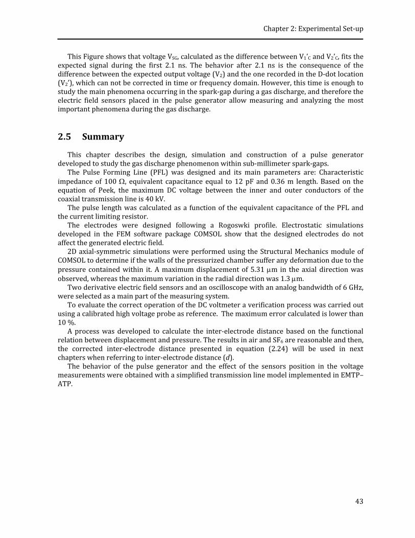
Chapter 2: Experimental Set‐up
43
This Figure shows that voltage VSG, calculated as the difference between V1’C and V2’C, fits the expected signal during the first 2.1 ns. The behavior after 2.1 ns is the consequence of the difference between the expected output voltage (V2) and the one recorded in the D‐dot location (V2’), which can not be corrected in time or frequency domain. However, this time is enough to study the main phenomena occurring in the spark‐gap during a gas discharge, and therefore the electric field sensors placed in the pulse generator allow measuring and analyzing the most important phenomena during the gas discharge. 2.5 Summary
This chapter describes the design, simulation and construction of a pulse generator developed to study the gas discharge phenomenon within sub‐millimeter spark‐gaps.
The Pulse Forming Line (PFL) was designed and its main parameters are: Characteristic impedance of 100 , equivalent capacitance equal to 12 pF and 0.36 m length. Based on the equation of Peek, the maximum DC voltage between the inner and outer conductors of the coaxial transmission line is 40 kV.
The pulse length was calculated as a function of the equivalent capacitance of the PFL and the current limiting resistor.
The electrodes were designed following a Rogoswki profile. Electrostatic simulations developed in the FEM software package COMSOL show that the designed electrodes do not affect the generated electric field.
2D axial‐symmetric simulations were performed using the Structural Mechanics module of COMSOL to determine if the walls of the pressurized chamber suffer any deformation due to the pressure contained within it. A maximum displacement of 5.31 m in the axial direction was observed, whereas the maximum variation in the radial direction was 1.3 m.
Two derivative electric field sensors and an oscilloscope with an analog bandwidth of 6 GHz, were selected as a main part of the measuring system.
To evaluate the correct operation of the DC voltmeter a verification process was carried out using a calibrated high voltage probe as reference. The maximum error calculated is lower than 10 %.
A process was developed to calculate the inter‐electrode distance based on the functional relation between displacement and pressure. The results in air and SF6 are reasonable and then, the corrected inter‐electrode distance presented in equation (2.24) will be used in next chapters when referring to inter‐electrode distance (d).
The behavior of the pulse generator and the effect of the sensors position in the voltage measurements were obtained with a simplified transmission line model implemented in EMTP–ATP.

Chapter 2: Experimental Set‐up
44

3 Chapter 3: Experimental Results
This chapter presents the experimental results of the investigation performed to obtain the breakdown characteristics of air, SF6 and argon, in the sub‐nanosecond time‐regime. These characteristics include breakdown voltage (Vb); resistive phase time of the switching time (R), pulse duration (FWHM) and arc‐resistance (Rarc). The second specific objective of this research work, namely: “to study the discharge channel formation and dynamic evolution by measuring electrical signals”, will be fulfilled at the end of the present chapter.
Laboratory tests in air, SF6 and argon at pressures between 174 and 774 kPa and inter‐electrode distances between 330 and 450 μm (by using the corrected gap distance described in equation (2.24) with d0 = 330 μm) are performed, and the derivative electric field signals detected by the D‐dot sensors located in the PFL and TL, and the breakdown voltage are recorded.
Even though five data are not a representative sample for statistical analysis, in this study five measurements were taken in each case and base on this information the average value and standard deviation were calculated. This number is sufficient to allow the calculation of the main parameters of interest in this study, but not so high to cause degradation on the electrodes surface. Determining the maximum number of discharges supportable by the electrodes before changing their initial conditions is out of the scope of this study.
3.1 Breakdown Voltage
To avoid contaminating the insulating gas, after each test, the spark‐gap volume was cleaned by replacing the tested gas volume. However, for the first measured shots, considerable scatter was observed in both, breakdown voltage and pulse shape. Therefore, it was necessary to trigger the spark‐gap numerous times until subsequent pulses became more unified and the scatter was decreased to an acceptable level within a series of measurements. This process is known as the “conditioning effect”, where weak points of the gap are destroyed by repetitive breakdown pulses (Malik et al., 1987). In this work and before the readings were taken, the spark‐gap electrodes were conditioned in air, at atmospheric pressure, by a 20 minutes repetitive discharge process. A 3 kV DC voltage was employed as a conditioning signal. After that process, subsequent pulses became more unified and scatter was decreased to an acceptable level within a series of measurements.
Results in Figure 3.1 show the breakdown voltage (Vb) as a function of the product pressure times inter‐electrode distance (pd), for each of the studied gases. In Figure 3.1 and hereinafter,

Chapter 3: Experimental Results
46
each point is the average of five measurements. As expected, SF6 has the highest breakdown voltage for a given pd value. All gases show a linear increase in breakdown voltage with respect to pd value; however, SF6 shows the greatest rate of increase of breakdown voltage under these conditions. This behavior is similar to the predicted by the theoretical and experimental models proposed by several authors (Kawaguchi et al., 1971, Malik et al., 1987, Kuffel et al., 2000) and equations (1.21) and (1.24). The maximum Relative Standard Deviation (RSD) respectively calculated for air, SF6 and argon is 2.9 %, 2.6 % and 6.4 %. The lowest deviation obtained for both air and SF6 (<3 %), means that for these two gases the spread of data is small. On the other hand, the large deviation obtained for argon, indicates a large data dispersion, which could be given by the reduced sensitivity of the voltage measuring system to the low voltage values recorded for this gas. Complete test data are included in Table A.3 in Appendix 4.
0
5
10
15
20
25
30
35
0 50 100 150 200 250 300 350 400
pd (kPa_mm)
Vol
tage
(kV
)
air
SF6
argon
Figure 3.1. Breakdown voltage measured in air (blue), SF6 (red) and argon (black) at different pd values
The correlation between the electric field strength E/p (at breakdown voltage) and the
product of pressure times inter‐electrode distance pd, is shown in Figure 3.2.
0
20
40
60
80
100
120
0 50 100 150 200 250 300 350 400pd (kPa_mm)
E/p
(kV
/(m
_kP
a)
AirSF6Ar
Figure 3.2. Breakdown field strength measured in air (blue), SF6 (red) and argon (black) at
different pd values These results agree well with Kuffel’s results displayed in Figure 3.3, in spite of the
differences in scales, where 1 bar.cm = 1 kPa_m.

Chapter 3: Experimental Results
47
In the pd range of this experimental work, the electric field strength in air and SF6 has been calculated between 52 and 35 kV/(m_kPa) and 96 and 89 kV/(m_kPa), respectively. For the same pd range Kuffel’s results show almost the same behavior in air (52 to 37 kV/(m_kPa)) and a good approximation in SF6 (102 to 90 kV/(m_kPa)). Additionally, experimental values in argon are between 18.3 and 7.5 kV/(m_kPa).
Figure 3.3. Breakdown field strength in air and SF6 at different pd values (Kuffel et al., 2000)
3.2 Derivative Electric Field Measurements
An example of the recorded derivative electric field signals in air at 774 kPa and d = 450 μm is shown in Figure 3.4. The continuous blue line corresponds to the signal measured by D‐dot1 placed at the high voltage side of the spark‐gap switch, and the dashed black line corresponds to the signal measured at the load side of the spark‐gap switch (D‐dot2).
Figure 3.4. Ddot sensors measurements for air at 774 kPa and d = 450 μm. Blue line: highvoltage side of the sparkgap switch (Ddot1). Dashed black line: loadside of the sparkgap switch (D
dot2) Figure 3.4 shows a wave reflection returning from the high voltage 50 M limiting resistor
located at the outer boundary of the pulse generator. The position of D‐dot1 (see Figure 2.12) is such that this reflection is recorded around 2.3 ns after the spark‐gap switch breaks down.

Chapter 3: Experimental Results
48
Therefore, 2.3 ns is the time‐limit of useful breakdown information that can be recorded from these signals. 3.2.1 CST Simulation
As described before, the D‐dot sensors register a wave reflection returning from the high‐voltage side of the pulse generator where the 50 M limiting resistor is located. A validation of the reflected waveform was obtained with an electromagnetic model implemented in the computer program CST Microwave Studio9 for a spark‐gap switch inter‐electrode distance d = 450 m in air. The proposed EM model used a discrete port (100 m resistive load) defined by an excitation signal with the following characteristics: Amplitude = 1 A, central frequency = 2 GHz, FWHM = 350 ps and rise‐time = 280 ps. The TL was terminated in a 100 resistive port and the PFL was terminated in an open circuit. The PFL electric field (D‐dot1) and TL electric field (D‐dot2) shown in Figure 3.5 were calculated in the places where the D‐dot sensors are located.
Figure 3.5. CST simulated electric fields, for d = 450 m in air. Blue line: Before the sparkgap (Ddot1). Dashed black line: After the sparkgap (Ddot2)
Based on results in Figure 3.5, it was corroborated that 2.3 ns after the spark‐gap breaks
down, the recorded waveforms are affected by the wave reflection returning from the high‐voltage side where the limiting resistor is located.
3.3 Postprocessing and Waveform Analysis
An example of the integrated waveforms, which show the voltage on the high voltage side of the spark‐gap switch (V1) and on the load side of the spark‐gap switch (V2), is shown in Figure 3.6. In this figure, the reflections in both voltage waveforms can be seen 2.3 ns after the spark‐gap breaks down. Additionally, a difference in the voltage fall‐time of both voltage waveforms in Figure 3.6 is observed, mainly due to the fact that the sensor D‐dot1, located at the high‐voltage side of the spark‐gap, is not able to register all the electric charge transferred during the breakdown, as it is explained in section 2.4. For this reason, the voltage signal V1 has a lower duration than the actual one. However, this fact does not affect the analysis of the signals.
9 http://www.cst.com/
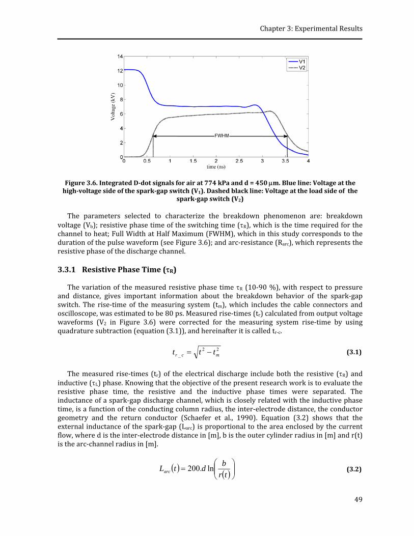
Chapter 3: Experimental Results
49
Figure 3.6. Integrated Ddot signals for air at 774 kPa and d = 450 m. Blue line: Voltage at the highvoltage side of the sparkgap switch (V1). Dashed black line: Voltage at the load side of the
sparkgap switch (V2) The parameters selected to characterize the breakdown phenomenon are: breakdown
voltage (Vb); resistive phase time of the switching time (R), which is the time required for the channel to heat; Full Width at Half Maximum (FWHM), which in this study corresponds to the duration of the pulse waveform (see Figure 3.6); and arc‐resistance (Rarc), which represents the resistive phase of the discharge channel.
3.3.1 Resistive Phase Time (R)
The variation of the measured resistive phase time R (10‐90 %), with respect to pressure and distance, gives important information about the breakdown behavior of the spark‐gap switch. The rise‐time of the measuring system (tm), which includes the cable connectors and oscilloscope, was estimated to be 80 ps. Measured rise‐times (tr) calculated from output voltage waveforms (V2 in Figure 3.6) were corrected for the measuring system rise‐time by using quadrature subtraction (equation (3.1)), and hereinafter it is called tr‐c.
22
_ mcr ttt (3.1)
The measured rise‐times (tr) of the electrical discharge include both the resistive (R) and
inductive (L) phase. Knowing that the objective of the present research work is to evaluate the resistive phase time, the resistive and the inductive phase times were separated. The inductance of a spark‐gap discharge channel, which is closely related with the inductive phase time, is a function of the conducting column radius, the inter‐electrode distance, the conductor geometry and the return conductor (Schaefer et al., 1990). Equation (3.2) shows that the external inductance of the spark‐gap (Larc) is proportional to the area enclosed by the current flow, where d is the inter‐electrode distance in [m], b is the outer cylinder radius in [m] and r(t) is the arc‐channel radius in [m].
tr
bdtLarc ln.200 (3.2)
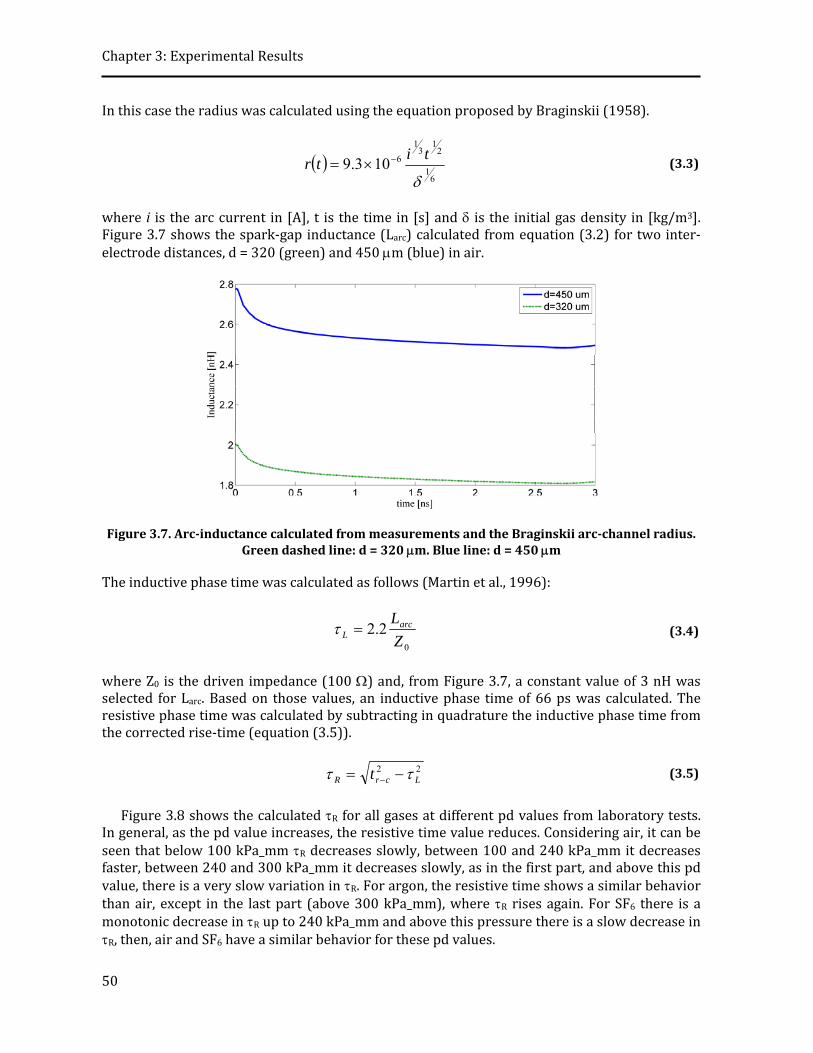
Chapter 3: Experimental Results
50
In this case the radius was calculated using the equation proposed by Braginskii (1958).
6
1
21
31
6103.9
titr (3.3)
where i is the arc current in [A], t is the time in [s] and is the initial gas density in [kg/m3]. Figure 3.7 shows the spark‐gap inductance (Larc) calculated from equation (3.2) for two inter‐electrode distances, d = 320 (green) and 450 m (blue) in air.
Figure 3.7. Arcinductance calculated from measurements and the Braginskii arcchannel radius. Green dashed line: d = 320 m. Blue line: d = 450 m
The inductive phase time was calculated as follows (Martin et al., 1996):
0
2.2Z
LarcL (3.4)
where Z0 is the driven impedance (100 ) and, from Figure 3.7, a constant value of 3 nH was selected for Larc. Based on those values, an inductive phase time of 66 ps was calculated. The resistive phase time was calculated by subtracting in quadrature the inductive phase time from the corrected rise‐time (equation (3.5)).
22LcrR t (3.5)
Figure 3.8 shows the calculated R for all gases at different pd values from laboratory tests.
In general, as the pd value increases, the resistive time value reduces. Considering air, it can be seen that below 100 kPa_mm R decreases slowly, between 100 and 240 kPa_mm it decreases faster, between 240 and 300 kPa_mm it decreases slowly, as in the first part, and above this pd value, there is a very slow variation in R. For argon, the resistive time shows a similar behavior than air, except in the last part (above 300 kPa_mm), where R rises again. For SF6 there is a monotonic decrease in R up to 240 kPa_mm and above this pressure there is a slow decrease in R, then, air and SF6 have a similar behavior for these pd values.

Chapter 3: Experimental Results
51
0
200
400
600
800
1000
1200
1400
0 50 100 150 200 250 300 350 400pd (kPa_mm)
resi
stiv
e ph
ase
tim
e (p
s)
air
SF6
Argon
Figure 3.8. Resistive phase time for air (blue), SF6 (black) and argon (red) at different pd values from laboratory tests
Despite the slope changes observed in Figure 3.8, a logarithmic decreasing trend is observed
for the three tested gases, with a correlation coefficient of 0.87 for argon and 0.96 for air and SF6. Additionally, Figure 3.8 shows that in air R reduces from 1160 ps at 57 kPa_mm to 650 ps at 350 kPa_mm, and then the ratio between those values is 0.56. In argon and SF6 this ratio is 0.73 and 0.47, respectively. In the case of SF6 this value corresponds to the ratio between the time at 98 kPa‐mm and the one at 350 kPa‐mm.
The resistive phase time R as a function of E/p was calculated for the three gases from laboratory test and the obtained results are plotted in Figure 3.9.
0
200
400
600
800
1000
1200
1400
0 20 40 60 80 100
E/p (kV/(m_kPa))
Res
isti
ve p
hase
tim
e (p
s)
air
SF6
argon
Figure 3.9. Resistive phase time for air (blue), SF6 (black) and argon (red) at different E/p values from laboratory tests
The plotted characteristics in this figure show that the resistive phase time in air and argon
are almost linear with respect to E/p. This is not the case for the highest R values, which correspond to the lower pd values. In the case of SF6, R follows a linear behavior for higher E/p values, and shows an almost constant value for the lower values of E/p, it means for the higher values of pd.
Complete information about the calculation of the resistive phase time is presented in Table A.4 in Appendix 4.

Chapter 3: Experimental Results
52
3.3.2 Full Width at Half Maximum (FWHM)
This parameter was estimated in the design phase (section 2.1.2) assuming that the generated pulse is square. Based on this assumption, equation (2.6) showed that the FWHM depends only on the equivalent capacitance of the charge transmission line (PFL) and the characteristic impedance of the transmission line (Z0).
Results in Figure 3.10 show the FWHM against the product between pressure and inter‐electrode distance (pd) for each of the studied gases. The FWHM value varies between 2.88 and 2.96 ns, with a maximum RSD of 2.14 %. From measurements it is possible to affirm that FWHM is almost a constant parameter which is independent on the type of gas, the pressure and the inter‐electrode distance.
2,87
2,88
2,89
2,90
2,91
2,92
2,93
2,94
2,95
2,96
2,97
0 50 100 150 200 250 300 350 400
pd (kPa_mm)
FW
HM
(ns
)
airSF6argon
Figure 3.10. Full Width at Full maximum FWHM for air (blue), SF6 (black) and argon (red) at different values of pd from laboratory tests
3.3.3 Arcresistance (Rarc)
Arc‐resistance is one of the parameters of interest when studying the discharge channel formation and its dynamic evolution, and therefore it has been analyzed in several works using different gases, pressures and inter‐electrode distances (Akiyama et al., 1988, Engel et al., 1989, Greason, 1999).
To calculate the arc‐resistance, the voltage drop across the spark‐gap (VSG) and the current through the transmission line flowing towards the load (i) were calculated for air, SF6 and argon from experimental results obtained at pressures between 174 and 774 kPa and inter‐electrode distances between 330 and 450 μm.
Voltages V1 and V2 calculated from the signals of the D‐dot sensors were corrected following the procedure described in section 2.4. Then, VSG was calculated as the difference between them. Afterwards, the resistive voltage (VR) was numerically calculated by subtracting the arc‐inductance calculated with equation (3.2) from the voltage drop across the spark‐gap.
Figure 3.11 shows the voltage drop across the spark‐gap (red line), the inductive voltage (green line) and the resistive voltage (blue line), calculated from experimental results for air at 774 kPa and d = 450 μm. Note that the voltage has the same behavior described from the ATP simulations in Figure 2.25. Same procedure was followed for all pd values in air, SF6 and argon, and a similar behavior as the one shown in Figure 3.11 was observed.
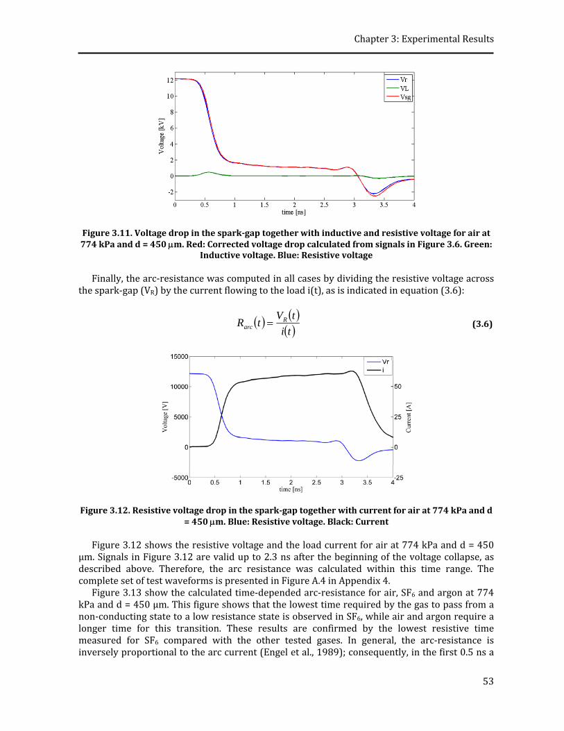
Chapter 3: Experimental Results
53
Figure 3.11. Voltage drop in the sparkgap together with inductive and resistive voltage for air at 774 kPa and d = 450 m. Red: Corrected voltage drop calculated from signals in Figure 3.6. Green:
Inductive voltage. Blue: Resistive voltage Finally, the arc‐resistance was computed in all cases by dividing the resistive voltage across
the spark‐gap (VR) by the current flowing to the load i(t), as is indicated in equation (3.6):
ti
tVtR R
arc (3.6)
Figure 3.12. Resistive voltage drop in the sparkgap together with current for air at 774 kPa and d = 450 m. Blue: Resistive voltage. Black: Current
Figure 3.12 shows the resistive voltage and the load current for air at 774 kPa and d = 450
μm. Signals in Figure 3.12 are valid up to 2.3 ns after the beginning of the voltage collapse, as described above. Therefore, the arc resistance was calculated within this time range. The complete set of test waveforms is presented in Figure A.4 in Appendix 4.
Figure 3.13 show the calculated time‐depended arc‐resistance for air, SF6 and argon at 774 kPa and d = 450 μm. This figure shows that the lowest time required by the gas to pass from a non‐conducting state to a low resistance state is observed in SF6, while air and argon require a longer time for this transition. These results are confirmed by the lowest resistive time measured for SF6 compared with the other tested gases. In general, the arc‐resistance is inversely proportional to the arc current (Engel et al., 1989); consequently, in the first 0.5 ns a

Chapter 3: Experimental Results
54
fast resistance transition from some k to tens of Ohms is observed, and after that it is observed an almost flat behavior with a small variation in the arc‐resistance value.
Figure 3.13. Arcresistance calculated from measurements for air (blue line), SF6 (red line) and argon (black line) at 774 kPa and 450 m
Figure 3.14 shows the arc‐resistance calculated for the three gases at pressures between 174
and 674 kPa and inter‐electrode distances between 330 and 436 μm. The results for SF6 and argon in Figure 3.14 show that the transition from a non‐conducting state to a low resistance state is faster at higher pd‐values; however, this is not completely clear for air.

Chapter 3: Experimental Results
55
Figure 3.14. Arcresistance calculated from measurements for air (blue line), SF6 (red line) and argon (black line). Pressure between 174 and 674 kPa and d between 330 and 436 m
Figure 3.15 shows the time‐dependant arc‐resistance from measurements for air at different
pd values. Based on this figure, the transition from a non‐conducting state to a low resistance state is faster at higher pd‐values, and for all cases the arc‐resistance begins in values of some k and falls until a few tens of Ohms.
Figure 3.15. Arcresistance calculated from measurements for air at different values of pd 3.4 Pulse Repetition Frequency (PRF)
The recovery phase refers to the time for recovering the dielectric properties of the gas so that the voltage can be reapplied to it (see Figure 1.8). Most spark‐gaps require recombination and attachment of electrons in the recovery phase. This leads to the recovery characteristics that limit the PRF of switch operation. In addition, in some cases, gas processes may occur rapidly but the gas is then left in a highly heated state. It means that the mean free path of stray charges is much higher and reapplication of voltage may initiate an avalanche. Thus, the gas should not only be de‐ionized but also be cooled and homogenized to allow voltage recovery. At very high pressures, the recovery processes are such that the recovery time may decrease significantly, in part because of the intense cooling of the arc plasma.
The pulse repetition frequency (PRF) as a function of pd and applied voltage (Vg) was calculated for air from laboratory tests using the same experimental set‐up described in Figure 2.20. The PRF was calculated as the inverse of the time between pulses (Td) (Figure 3.16). This

Chapter 3: Experimental Results
56
value was measured using the peak detection mode of a DSO6104A Agilent oscilloscope with the trigger level adjusted at 0.1 times the maximum voltage recorded in the single pulse test. Due to the jitter and the statistical behavior of the gas discharge, the value of Td changes between shots; then, the horizontal resolution time of the oscilloscope was adjusted for capturing at least six pulses.
Figure 3.16. Pulse Repetition Frequency measurement. At least six shots were captured in the oscilloscope. Td is the time between pulses
Figure 3.17 shows the PRF laboratory tests results for air at different pd values. The range of
applied voltages (Vg) was 5 to 50 kV. It was increased in steps of 5 kV, and for each voltage the PRF was calculated.
0
2
4
6
8
10
12
14
16
18
0 10 20 30 40 50 60
Applied voltage (kV)
PRF
(kH
z)
pd = 98.4 kPa_mmpd = 140.6 kPa_mmpd = 186.8 kPa_mmpd = 236.5 kPa_mmpd = 293.9 kPa_mm
Figure 3.17. Pulse Repetition Frequency measurement in air. Applied voltage between 5 and 50 kV at different values of pd
The reported PRF corresponds to the mean value of the six pulses, including its respective
deviation. Values between 0.3 and 16 kHz were recorded, depending on the pd value and the applied voltage. The PRF is bigger at lower pd values and higher Vg.
The pulse repetition frequency in non‐flowing gas spark‐gaps is limited by the recovery time of the gas, which includes the time needed by the gas to eliminate the remaining ions, via recombination or attachment; and the time the gas takes to recover its original density. These
TdPulse

Chapter 3: Experimental Results
57
processes take up to a few milliseconds, depending of the power involved in the discharge (Mac Gregor et al., 1997). Therefore, the experimental results must be used carefully, especially at high PRF’s. Complete data about PRF calculation is presented in Table A.5 in Appendix 4.
3.5 Switching Efficiency
The efficiency parameter (Eff) proposed by Christophorou et al. (1987) was it is described in equation (1.25) and is recalled here as equation (3.7).
2
1
b
CV
VEff (3.7)
In equation (3.7), VC is the voltage across the two electrodes during the stationary phase (see
Figure 1.8) and Vb is the breakdown voltage. On the other hand, Bluhm (2006) proposed that the energy loss (Ws) can be estimated assuming that a considerable energy consumption occurs only during the commutation phase (see Figure 1.8), as it is described in equation (1.26) and is recalled in equation (3.8).
5Rmb
s
IVW
(3.8)
In equation (3.8), Vb is the breakdown voltage, Im is the maximum current, and R is the resistive phase time. Assuming that the energy stored in the PFL (WC) is:
2
2
1bC CVW (3.9)
The switching efficiency can be described as the ratio of the energy transferred by
discharges in the transmission line and the energy accumulated in the PFL before the switch breaks down. Therefore, an alternative method to calculate the switching efficiency is:
C
SC
W
WWEff
2 (3.10)
Theoretically, a loss free plasma spark‐gap has a switching efficiency of 1. However, only
under some specific conditions and topologies, efficiency greater than 0.93 has been reported (Liu et al., 2009). Figure 3.16 shows the switching efficiency obtained for air, SF6 and argon at different values of pd from laboratory tests and by using the equations (3.7) (filled markers) and (3.10) (unfilled markers). A complete set of switching efficiency calculations is presented in Table A.6 in Appendix 4.
Results in Figure 3.18 show that both equations used for the calculation of efficiency give similar values. By using equation (3.7) the efficiency values for air, SF6 and argon are 0.77 to 0.85, 0.83 to 0.97 and 0.88 to 0.92, respectively; and by using equation (3.10) efficiency values are 0.81 to 0.89, 0.91 to 0.96 and 0.86 to 0.91 for air, SF6 and argon, respectively. Additionally, it is observed that by using equation (3.10) the efficiency is higher at larger pd‐values.

Chapter 3: Experimental Results
58
0,0
0,2
0,4
0,6
0,8
1,0
1,2
0 50 100 150 200 250 300 350 400
pd (kPa_mm)
Eff
icie
ncy
Air Eff1
Air Eff2
SF6 Eff1
SF6 Eff2
Argon Eff1
Argon Eff2
Figure 3.18. Switching efficiency for air, SF6 and argon at different values of pd. Filled markers: equation (3.6). Unfilled markers: equation (3.9)
Based on results in Figure 3.18, it is possible to affirm that SF6 is the most efficient gas for
switching under the pd conditions of this work, followed by argon. Nevertheless, in all cases switching efficiency is around 0.8 and 0.9. 3.6 Summary
This chapter presents the experimental results of the investigation about the breakdown characteristics in the sub‐nanosecond time regime for air, SF6 and argon.
As expected, SF6 has the highest breakdown voltage for a given pd value. All gases show a linear increase in breakdown voltage with respect to the pressure‐distance relation. This behavior is similar to the predicted by the theoretical and experimental models.
The effect of the high impedance boundary in the recorded waveforms was studied with an electromagnetic model implemented in CST.
The inductance of a spark‐gap was calculated and based on that, the inductive phase time was estimated and subtracted from the measured rise‐time, obtaining in this way the resistive phase time.
Based on the arc‐resistance signatures, the time required by the gas to pass from a non‐conducting state to a low resistance state is lower in SF6, followed by air, while argon requires more time for this transition.
The pulse repetition frequency (PRF) as a function of pd and applied voltage (Vg) was calculated for air. Values between 0.3 and 16 kHz were recorded, depending on the pd value and the applied voltage. At lower pd value and higher Vg, the bigger PRF.
Finally, by using two different equations, switching efficiencies between 0.8 and 0.9 were calculated. Based on the results, it is possible to affirm that SF6 is the most efficient gas for switching under the pd conditions used in this thesis.

4 Chapter 4: Sparkgap Modeling
Laboratory tests results and calculated data obtained in Chapter 3 are compared with existing theoretical and empirical predictions. Some empirical fits for experimental data are presented. An improved TL model is implemented in EMTP‐ATP and its results are compared with the experimental data.
In this chapter, the specific objectives three and four “to compare the results with the most widely accepted electrical discharge channel models” and “to propose a sparkgap model to predict the waveform characteristics of the generated signals” are reached.
4.1 Comparison of Results and Existing Models
In this section, some of the parameters selected to characterize the breakdown phenomenon, called resistive phase time of the switching time (R), arc‐resistance (Rarc) and pulse repetition frequency (PRF) are compared with models proposed in literature by several authors.
4.1.1 Resistive Phase Time (R)
The pd dependence of the measured resistive phase time for the three gases was compared with the equation proposed by Martin (1965), and in the case of air it was also compared with the equation of Sorensen and Ristic (1977). These equations were described in section (1.5.4); in the case of the equation of Martin (equation (1.29)), the rise of the signal is not exponential, and multiplying by 1.8 converts the e‐fold rise‐time to a 10‐90% rise‐time (Carboni et al., 2002).
A comparison between measured and calculated values using Martin´s and Sorensen and Ristic´s equations, for air, are presented in Figure 4.1. From the curves in this figure it can be seen that, whereas Martin´s equation shows discrepancies of up to a factor of 2, Sorensen and Ristic´s equation shows differences up to 1.5. Laboratory tests reported by Sorensen and Ristic were performed using nitrogen at pressures between 234 and 662 kPa with inter‐electrode distances from 50 to 500 μm, obtaining a variation of the electric field in the gap from 10 to 75 kV/mm (Sorensen et al., 1977). Since present investigation was conducted in air at pressures in the range from 174 to 774 kPa, and inter‐electrode distances between 330 and 450 μm, a similar behavior should be expected. However, results indicate that Sorensen and Ristic´s equation predicts a much slower rise‐time than occurs in practice. Scott et al. (1978) report similar differences for nitrogen at pressures between 200 and 1400 kPa and an inter‐electrode distance of 100 μm.
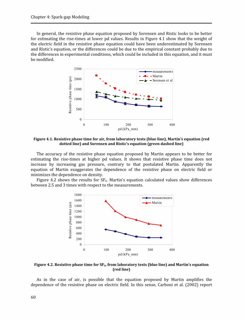
Chapter 4: Spark‐gap Modeling
60
In general, the resistive phase equation proposed by Sorensen and Ristic looks to be better for estimating the rise‐times at lower pd values. Results in Figure 4.1 show that the weight of the electric field in the resistive phase equation could have been underestimated by Sorensen and Ristic’s equation, or the differences could be due to the empirical constant probably due to the differences in experimental conditions, which could be included in this equation, and it must be modified.
0
500
1000
1500
2000
2500
0 100 200 300 400pd (kPa_mm)
Res
istiv
e ph
ase
time
(ps)
measurementsMartinSorensen et al
Figure 4.1. Resistive phase time for air, from laboratory tests (blue line), Martin’s equation (red dotted line) and Sorensen and Ristic’s equation (green dashed line)
The accuracy of the resistive phase equation proposed by Martin appears to be better for
estimating the rise‐times at higher pd values. It shows that resistive phase time does not increase by increasing gas pressure, contrary to that postulated Martin. Apparently the equation of Martin exaggerates the dependence of the resistive phase on electric field or minimizes the dependence on density.
Figure 4.2 shows the results for SF6. Martin’s equation calculated values show differences between 2.5 and 3 times with respect to the measurements.
0
200
400
600
800
1000
1200
1400
1600
1800
0 100 200 300 400pd (kPa_mm)
Res
istiv
e ph
ase
time
(ps)
measurementsMartin
Figure 4.2. Resistive phase time for SF6, from laboratory tests (blue line) and Martin’s equation (red line)
As in the case of air, is possible that the equation proposed by Martin amplifies the
dependence of the resistive phase on electric field. In this sense, Carboni et al. (2002) report

Chapter 4: Spark‐gap Modeling
61
that differences of two or more times where found when experimental results obtained for different gases under several pressure conditions and constant inter‐electrode distance were compared with the resistive phase equation proposed by Martin. In that paper the authors suggest that equation of Martin is pessimistic in most cases.
In the case of argon, differences larger than 10 times were observed when the resistive phase time was calculated from the equation of Martin and compared with the experimental results. Due to those differences results for the case of argon were not plotted.
Results in Figures 4.1 and 4.2 suggest that in the case of air, the equation of Sorensen and Ristic underestimates the rise‐time dependence on the electric field, while the equation of Martin overestimates such dependency. A similar behavior was observed in the case of SF6 by using Martin’s equation. Moreover, the empirical constants proposed by those authors do not fit well with the experimental results.
Considering these aspects, a linear regression was performed with E0 as the independent variable and dependent variable τR, the other parameters of the equations of Martin (equation (1.29)) and Sorensen and Ristic (equation (1.30)) were assumed as constants. In this case, a power regression was employed, which depends on the amplitude A and an exponent b included in the fitting function, as shown in equation (4.1).
b
R AE0 (4.1)
Based on the regression model, a change in the electric field, in both the equation of Martin
and the equation of Sorensen and Ristic, is proposed. Equations (4.2) and (4.3) show the modified equations.
21
031
05
6
0
1
ZE
kR
ns (4.2)
21
31
05
6
0
2 pZE
kR
ns (4.3)
where and 0 are the density of the gas in the gap and the density of the air at S.T.P., respectively, Z0 is the impedance of the circuit driving the conducting channel, p is the gas pressure in [kPa], and E0 is the electric field along the channel in [kV/mm]. The empirical constants are k1 = k2 = 60 in air, k1 = 60 and k2 = 79 in SF6, and k1 = 6.5 and k2 = 8 in argon.
Figures 4.3, 4.4 and 4.5 show the resistive phase time calculated from equations (4.2) and (4.3) compared with the experimental results for air, SF6 and argon, respectively.
Comparing the experimental results in air and SF6 with the calculated ones from the equations (4.2) and (4.3), it is observed that the results obtained from the empirical models fit well the laboratory test results. The coefficient of determination (R2) calculated to determine how well the equations (4.2) and (4.3) represent the experimental data in air are 94.7% and 95%, respectively, while in the case of SF6 the coefficient of determination (R2) is 96% for both equations. On the other hand, some differences are observed between the calculated R and the theoretical one in argon at lower values of pd (R2 < 1%). It appears that in that pd range the resistive phase time does not increase by increasing pressure as proposed in equations (4.2) and (4.3). Therefore, in the case of argon equations overstate the dependence of the resistive phase time on pressure (or gas density) or understate the dependence on electric field.

Chapter 4: Spark‐gap Modeling
62
0
200
400
600
800
1000
1200
0 50 100 150 200 250 300 350 400pd (kPa_mm)
rise
tim
e (p
s)
measurementsequation (4.1)equation (4.2)
Figure 4.3. Resistive phase time for air. Blue line: laboratory tests, red dotted line: equation (4.2), black dashed line: equation (4.3)
0
100
200
300
400
500
600
700
0 50 100 150 200 250 300 350 400pd (kPa_mm)
Res
isti
ve p
hase
tim
e (p
s)
measurements
equation (4.1)
equation (4.2)
Figure 4.4. Resistive phase time for SF6. Blue line: laboratory tests, red dotted line: equation (4.2), black dashed line: equation (4.3)
0
100
200
300
400
500
600
700
800
900
1000
0 50 100 150 200 250 300 350 400pd (kPa_mm)
Res
isti
ve p
hase
tim
e (p
s)
measurements
equation (4.1)
equation (4.2)
Figure 4.5. Resistive phase time for argon. Blue line: laboratory tests, red dotted line: equation (4.2), black dashed line: equation (4.3)

Chapter 4: Spark‐gap Modeling
63
Equations (4.2) and (4.3) have almost the same behavior. Hence, any of them can be used in the calculation of the resistive phase time in the pd range described in this investigation.
4.1.2 Arcresistance (Rarc)
In this section, the arc‐resistance calculated from measurements presented in section 3.3.3 is compared with some of the most accepted models. The resistance equations analyzed are those reported by Toepler (quoted by Montaño et al., 2006, Bluhm, 2006), Vlastos (1972), Kushner et al. (1985) and Sorensen and Ristic (1977). These theoretical and empirical equations are numerically evaluated for the present experimental conditions and by using the experimental waveforms and the arc‐channel radius of Braginskii (1958). Figure 4.6 shows the results for air at 774 kPa and d = 450 μm.
Figure 4.6. Arcresistance calculated for air at 774 kPa and 450 m. Measurements (blue line), Kushner (green line), Sorensen and Ristic (red line), Toepler (black line) and Vlastos (dotted line) The arc‐resistance models presented in Figure 4.6 show a similar behavior predicting the
value of the arc‐resistance for the initial stage of the discharge, i.e. between 50 ps and 400 ps (Table 4.1). The models obtained theoretically by Kushner et al. and Vlastos assume that a high degree of ionization exists in the channel; and therefore the Spitzer conductivity is reached, according to which the arc‐resistance decreases in proportion to the electron temperature as Te‐3/2, while Toepler’s and Sorensen and Ristic’s equations are empirical.
Vlastos’ equation is an inverse integral equation obtained when the energy balance in the channel is considered in the derivation of the arc‐resistance, without including the radiative loss term. This equation fits well the experimental results for the times after the maximum arc current (t > 400 ps). The equation given by Toepler has also the inverse integral form, but for times after the fast transition discharge (t > 400 ps) is not as truthful as Vlastos’ equation. The discrepancy in results obtained using the Toepler’s equation (R2 = 92%) could be attributed to either the empirical nature of the equation or to its independence of the arc‐channel conductivity and radius. On the other hand, inaccuracies in the arc‐resistance equation given by Sorensen and Ristic could be due to the experimental conditions at which it was obtained.
For times greater than 400 ps, experimental results follow the tendency given by Kushner’s and Vlastos’ equations (R2 equal to 98% and 97%, respectively). However, the best agreement for times between 50 ps and 2.3 ns, is observed with Kushner’s equation (Table 4.1). This equation is an inverse exponential equation derived without the strict application of the energy balance equation.

Chapter 4: Spark‐gap Modeling
64
Figure 4.7 shows the arc‐resistance calculated for SF6 and argon at 774 kPa and d = 450 μm, following the previously described procedure used for air.
Figure 4.7. Arcresistance calculated for SF6 and argon at 774 kPa and 450 m. Measurements (blue line), Kushner (green line), Sorensen and Ristic (red line), Toepler (black line) and Vlastos
(dotted line) In general, the arc‐resistance models presented in Figure 4.7 show some discrepancies
predicting the value of the arc‐resistance for all the times. However, the results obtained by using the equations given by Kushner et al., Vlastos and Sorensen et al., show a similar behavior predicting the arc‐resistance value for the initial stage of the discharge in SF6 (R2 equal to 99%, 99% and 100%, respectively). For SF6 and times greater than 250 ps, the equation proposed by Kushner et al. follows the tendency of the experimental results (R2 = 82%). In argon the equation given by Sorensen and Ristic follows the tendency of the experimental results just for only the first 750 ps.
The coefficient of determination (R2) was calculated by using the 100 signals recorded in this work; however, in Table 4.1 only the values obtained for p = 774 kPa are presented. Additionally, for the calculation of R2 the waveforms were divided in two regions according to the description in Fig. 1.8 (p. 12), a commutation phase and a stationary phase.
Table 4.1. Coefficient of determination (R2) for different gases and p = 774 kPa
Gas Phase Kushner (%)
Vlastos (%)
Toepler (%)
Sorensen and Ristic (%)
Commutation 98,5 96,7 99,7 99,9 Air Stationary 97,5 97,4 95,1 87,7
Commutation 99,4 96,5 87,3 99,8 SF6 Stationary 87,4 73,1 74,1 53,6
Commutation 97,9 95,5 93,7 99,0 Argon Stationary 94,8 93,5 93,3 95,2
As described at the end of Chapter 1, several studies have been carried out using the arc‐
resistance equations presented in Table 1.2. A common conclusion obtained in these studies and in the present research work is that the equation of Kushner et al. offers the best fit for the experimental results. Akiyama (1988) and Engel (1989) found that the equation given by Kushner et al. offers the best approximation for the calculated arc‐resistance value obtained for experiments in air at atmospheric pressure and d = 10 mm, with 700 ns rise‐time pulses and a duration of 4 s. Similar conclusions were reported by Montaño et al. (2006) based on two sets

Chapter 4: Spark‐gap Modeling
65
of laboratory tests, one applying 10/350 µs current impulses to a 10 mm spark‐gap, and other with lightning voltage impulses applied to a 128 mm spark‐gap by a Marx generator.
The constant of proportionality included in the equation of Kushner et al. depends on the experimental conditions and it has been estimated by several authors (Engel et al., 1989, Montaño et al., 2006). In the present research work, a multiple linear regression was performed with E/p and d as the independent variables and the constant value calculated from the experimental results as dependent variable. The 100 measurements recorded in this study were used in this process.
Based on this process, the relation between the pressure reduced electric field at breakdown times the inter‐electrode distance (d*E/p) is proposed as a constant of proportionality, which depends on the type of gas, pressure and inter‐electrode distance. The modified Kushner´s equation is presented here as equation (4.4).
5
1
62
3
iA
pdd
p
ERarc (4.4)
where E in [V/m] is the breakdown electric field, d in [m] is the inter‐electrode distance, p in [kPa] is the pressure, A in [m2] is the time depending arc‐channel area calculated from the radius of Braginskii, and i in [A] is the current.
The unit of equation (4.4) does not correspond to an electrical resistance (). This fact indicates that an additional constant should be included in the equation, whose units are N1/2/m approximately; however, due to the good fit of the new equation with respect to the experimental results, the additional constant was not included in this work.
Figure 4.8. Arcresistance calculated for a) air, b) SF6 and c) argon at 774 kPa and 450 m.
Measurements (blue line) and modified Kushner’s model (green line)

Chapter 4: Spark‐gap Modeling
66
In Figure 4.8 the arc‐resistance calculated from equation (4.4) is compared with the resistance estimated from measurements at 774 kPa and an inter‐electrode distance of 450 μm for: a) air, b) SF6, c) argon. A similar behavior between the measurements and the modified Kushner’s model proposed by the author is observed in Figure 4.8 for air and SF6. In the case of argon, theoretical and experimental values show a similar behavior only in the initial stage (t < 400 ps), but for longer times the predicted arc‐resistance values exceed the measured ones.
4.1.3 Pulse Repetition Frequency (PRF)
The free voltage recovery process can be divided in two phases (Moran et al., 1991). The first phase is the plasma channel gas deionization that follows breakdown. The time duration of this phase is in the order of 10 μs. The second phase is the cooling process of the neutral gas, which provides the gas with its DC hold–off voltage. The time duration of this phase takes a few milliseconds.
The switching performance of closing switches is restricted up to few tens of kiloHertz in gases like air, nitrogen, hydrogen and so on (Moran et al., 1991, MacGregor et al., 1995). The operation at very high pressures (>1000 kPa) improves the PRF behavior due to the increased heat capacity.
Laboratory tests results in air at different pressures and applied voltages were presented in Figure 3.17. PRFs between some Hertz and 16 kHz were reported. For the maximum value of PRF the time between pulses (63 s) is much lower than that required for the voltage recovery processes described above. That means that the gas had not fully recovered when a new discharge occurred through the gap. As a result, the voltage level at which the subsequent discharges occurred should be lower than the voltage at which the first discharge occurred (Vb).
The charging time constant of the PFL () is calculated as the product of the limiting resistor (RS) and the PFL capacitance (C), and during the charging phase, the voltage across the PFL (VC) can be calculated as:
CRt
g
t
gCSeVeVV 11 (4.5)
where Vg is the applied voltage, RS = 50 M and C = 12 pF. Figure 4.9 shows the normalized voltage at the charging line (PFL). After 3 ms the charging voltage is close to the DC hold–off voltage.
In Figure 3.17 were presented the PRF obtained from laboratory tests results at different pd values and applied voltages. In Figure 4.9 are included the mentioned results for: a) Vg = 50 kV and b) Vg = 10 kV.
Figure 4.9 can be interpreted as follows: if 50 kV are applied across the spark‐gap in air at 674 kPa, a PRF of 16 kHz (Td = 63 s) is obtained, this value corresponds to the solid black line in the Figure 4.9a. Therefore, under these conditions the gas had not fully recovered its insulating properties and hence the voltage needed to produce a subsequent breakdown is 10% of the expected voltage. Similar results were observed for different values of pressure. On the other hand, by applying 10 kV (Figure 4.9b) the time between pulses was longer, and for this reason the breakdown occurs at higher voltage levels.
This result demonstrates that although PRFs in the order of tens of kHz were recorded, the energy per pulse was significantly reduced, and therefore, this energy is a function of the applied voltage and the pd value.

Chapter 4: Spark‐gap Modeling
67
0
0,05
0,1
0,15
0,2
0,25
0,3
0,35
0,4
0,45
0,5
0 100 200 300 400Charging time (us)
Nor
mal
ized
vol
tage
p = 274 kPap = 374 kPap = 474 kPap = 574 kPap = 674 kPa
Vg = 50 kV
a)
0
0,1
0,2
0,3
0,4
0,5
0,6
0,7
0,8
0,9
1
0 500 1000 1500 2000Charging time (us)
Nor
mal
ized
vol
tage
Vg = 10 kVp = 274 kPap = 374 kPap = 474 kPa
p = 574 kPa
b)
Figure 4.9. Charging voltage (blue line) and voltage for subsequent discharges at different values of pressure and applied voltage. a) Vg = 50 kV. b) Vg = 10 kV. Notice the inverse relationship
between the PRF and voltage level Several regression models were used to determine the most appropriate representation of
the measured PRF as a function of the two independent variables, applied voltage and pd. The objective of this regression analysis is to understand how the PRF changes when any one of the independent variables is varied, while the other independent variable is held fixed. Several models provided an adequate fit for the measured data with correlation coefficients R2 = 0.99. However, a simple regression model depending on the applied voltage and the pd relationship presented in equation (4.6) was selected.
gVpdPRF 34
120 (4.6)
where PRF is given in [kHz], pd in [kPa_mm] and Vg in [kV].
Implementing this model, the pulse repetition frequency was calculated and compared with the experimental results as shown in Figure 4.10.

Chapter 4: Spark‐gap Modeling
68
0
2
4
6
8
10
12
14
16
18
0 10 20 30 40 50Applied voltage (kV)
PRF
(kH
z)
measurement (98.4 kPa_mm)Model (98.4 kPa_mm)measurement (186.8 kPa_mm)Model (186.8 kPa_mm)measurement (293.9 kPa_mm)Model (293.9 kPa_mm)
Figure 4.10. Pulse Repetition Frequency in air at 98.4 kPa_mm (blue), 186.8 kPa_mm (red) and (293.9 kPa_mm). Results from measurements (square markers) and equation (4.6) (dotted lines) The empirical model proposed in the equation (4.6) reproduces the experimental results
within the range of voltages, pressures and inter‐electrode distances employed in this thesis, with a maximum error of 20%. However this model must be validated in further works.
Rahaman (2007) describes that by using SF6 the rapid build up of metal fluoride (FeF2/FeF3) on the stainless steel reduces the efficiency of the electron emission from the bombardment of positive ions; and then, the end of lifetime can be fast for this electrode material when SF6 is used in the closing switch.
4.2 EMTPATP Modeling and Transmission Line Simulations
Once analyzed the main parameters associated with the gas discharge in air, SF6 and argon within the specific range of pressures and inter‐electrode distances used in laboratory tests, it is possible to predict the waveform and main characteristics of the pulses produced by different types of generators based on closing switches, modifying the transmission line model presented in section 2.4.
In Figure 4.11 the PFL distributed parameters circuit model (PFL1) is connected to the spark‐gap model (S‐G). After that, TL is modeled as a distributed parameters circuit model (TL1). Additionally, the new model includes two small transmission lines that represent the effect of the UHMW‐PE insulator (PFL2 and TL2). Finally, the 100 load resistance (R) is connected to the transmission line models.
Figure 4.11. EMTPATP Transmission Line model of the pulse generator including both, the PFL and the TL sections, the sparkgap model (SG) based on equation (4.3), a the 100 load
resistance (R) and the location of the voltage (V) sensors

Chapter 4: Spark‐gap Modeling
69
At high pressure, discharge modeling is generally complex because of the large number of microscopic phenomena which are involved in the pre‐breakdown and breakdown (Pécastaing et al., 2001). Since it is not possible to include all the processes in the EMTP‐ATP10 simulation, a simplified model of the spark‐gap switch was introduced. This model includes the arc‐resistance equation developed in section 4.1.2 (equation (4.4)) and a constant arc‐inductance of 6 nH in series. The final value of the arc‐inductance was determined by error and trial in order to obtain a good agreement with experimental results. Parameters of the circuit model showed in the Figure 4.11 are the same presented before in Table 2.6.
Despite EMTP‐ATP simulation does not take electromagnetic waves into account, the simulations are possible considering the following:
The transmission line is supposed to be used in the TEM mode. Non‐TEM modes
generated near the discharge or at the boundaries between the S‐G and TL1, TL1 and TL2, and TL2 and R were neglected.
It is possible to include some small transmission line models in the simulation circuit in order to model the effect of the UHMW‐PE insulator used in the pressurized chamber.
The mismatching at connections of the lines TL1 and TL2 was included. The generated signals have frequency components from low frequency up to 1 GHz;
however, the most energy is concentrated in the low frequency components, and therefore, the transmission line parameters variation with frequency is not significant and it can be neglected in the model implemented in EMTP‐ATP.
Figure 4.12 shows the voltage waveforms from laboratory test and the simulation of the
circuit in Figure 4.11 for air at 774 kPa and an inter‐electrode distance d = 450 m. The great agreement obtained enables the validation of the transmission line model presented above. Nevertheless, some differences are observed between the simulated FWHM pulse duration (2.76 ns), the FWHM value obtained from the laboratory test (2.9 ns) and the expected one presented in Table 2.4 (2.4 ns).
Figure 4.12. Measured and Simulated voltages for air at 774 kPa and d = 450 m. Red line and filled circles: charging voltage from measurement. Green line: charging voltage from simulation. Blue line and empty circles: output voltage from measurement. Black line: output voltage from
simulation
10 http://www.emtp.org

Chapter 4: Spark‐gap Modeling
70
These differences mean that the equivalent capacitance of the PFL (C) is higher that both capacitances, the used in the calculation of Table 2.4 and the one included in the simulations. To estimate the value of this additional capacitance, the charge stored in the PFL was calculated from the waveforms in Figure 4.12, and the experimental and simulated charges were subtracted. The additional charge in measurement with respect to the charge in the simulation is 12.8 nC, which corresponds to an additional capacitance of 1 pF.
This capacitance depends on two parameters: the transmission line topology and dimensions and the characteristics of the dielectric materials. The dimensions and topology of the PFL are fixed and were carefully included in the circuit model; therefore, this additional capacitance could be due to changes in the dielectric properties of the UHMW‐PE used in the pressurized chamber or due to a parasitic capacitance (CP) between the outer conductor of the PFL and the limiting resistor (RS) (see Figure 4.13).
Figure 4.13. Scheme of the PFL connected to the limiting resistor. C is the equivalent capacitance of the PFL and CP is the parasitic capacitance between the outer conductor of the PFL and the
limiting resistor An axial‐symmetric electrostatic simulation of the geometry in Figure 4.13 was performed
using COMSOL and so the PFL capacitance (C) and the parasitic capacitance (CP) were calculated. For simplicity, the transmission line section called PFL2 in Figure 4.11 was not included in the electrostatic simulation. Figure 4.14 shows the PFL‐RS model implemented in COMSOL11 and the resulting electric field. Note that there are some electric field lines between the PFL and the limiting resistor.
Figure 4.14. Axialsymmetric electrostatic simulation. a. Geometry. b. Electric field From the simulation results, the PFL and the parasitic capacitances are 11.6 pF and 1.09 pF,
respectively. The last value corresponds to the additional capacitance described before. Figure 4.15 shows the voltage waveforms from laboratory tests and the simulation of the
transmission line model of Figure 4.11 for air at 774 kPa and an inter‐electrode distance d = 450 m, including the additional capacitance (CP). In the figure, the output signal from the simulation (V2 model) shows almost the same behavior than the signal obtained from laboratory test (V2 Lab).
11 http://www.comsol.com
C
C
PFL
RSHV SourceS‐G
CP
CP
PFL Air
RS
a
b

Chapter 4: Spark‐gap Modeling
71
Figure 4.15. Measured and Simulated voltages for air at 774 kPa and d = 450 m including the parasitic capacitance. Red line and filled circles: charging voltage from measurement. Green line: charging voltage from simulation. Blue line and empty circles: output voltage from measurement.
Black line: output voltage from simulation Despite some small differences that persist in the PFL voltage signal (green line), it can be
affirmed that the proposed transmission line model reproduces the main parameters of the signals before and after the spark‐gap. The coefficient of determination (R2) calculated to determine how well the simulation results represent the experimental voltages recorded in the PFL and TL are 96.8% and 98.3%, respectively. Therefore, using this model it is possible to predict the waveform characteristics of the generated signals.
4.3 Summary
The arc‐resistance equation of Kushner et al. offers the best fit to the experimental results. A new constant for the equation of Kushner was proposed. It depends on the electric field at
breakdown, the gas pressure and the inter‐electrode distance. Results in air and SF6 by using the new equation fit well the experimental results. Important differences were observed in the case of argon.
For the maximum value of PRF recorded (16 kHz) the time between pulses is 63 s, which is much lower than that required for the voltage recovery processes. Therefore, the gas had not fully recovered when a new discharge occurred through the gap, and the voltage level at which the subsequent discharges occurred was lower than the static breakdown voltage.
A maximum error of 15% was obtained when the empirical model proposed in this thesis to estimate the PRF in air was used.
An improved transmission line model based on the one described in chapter 2 was proposed. The model of the spark‐gap includes the arc‐resistance equation proposed in this thesis and a constant arc‐inductance of 6 nH.
An additional capacitance of 1 pF was calculated. COMSOL simulation demonstrates that this additional capacitance corresponds to the parasitic capacitance between the outer conductor of the PFL and the limiting resistor RS.
EMTP‐ATP simulation results including the parasitic capacitance were developed. Simulated waveforms fit with experimental results in a better way than with the previous model.

Chapter 4: Spark‐gap Modeling
72
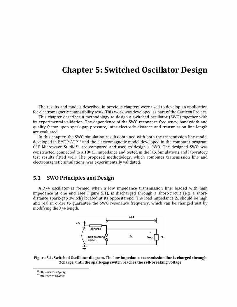
5 Chapter 5: Switched Oscillator Design
The results and models described in previous chapters were used to develop an application for electromagnetic compatibility tests. This work was developed as part of the Cattleya Project.
This chapter describes a methodology to design a switched oscillator (SWO) together with its experimental validation. The dependence of the SWO resonance frequency, bandwidth and quality factor upon spark‐gap pressure, inter‐electrode distance and transmission line length are evaluated.
In this chapter, the SWO simulation results obtained with both the transmission line model developed in EMTP‐ATP12 and the electromagnetic model developed in the computer program CST Microwave Studio13, are compared and used to design a SWO. The designed SWO was constructed, connected to a 100 , impedance and tested in the lab. Simulations and laboratory test results fitted well. The proposed methodology, which combines transmission line and electromagnetic simulations, was experimentally validated.
5.1 SWO Principles and Design
A λ/4 oscillator is formed when a low impedance transmission line, loaded with high impedance at one end (see Figure 5.1), is discharged through a short‐circuit (e.g. a short‐distance spark‐gap switch) located at its opposite end. The load impedance ZL should be high and real in order to guarantee the SWO resonance frequency, which can be changed just by modifying the λ/4 length.
Figure 5.1. Switched Oscillator diagram. The low impedance transmission line is charged through Zcharge, until the sparkgap switch reaches the selfbreaking voltage
12 http://www.emtp.org 13 http://www.cst.com/

Chapter 5: Switched Oscillator Design
74
For a real load impedance ZL, equations describing the operation of the oscillator can be found in Baum (2000) and Baum (2001).
The operation of SWO is described in terms of its resonance frequency and the rate at which the stored energy is transferred to the load; the quality factor (Q – factor) is the correct variable to describe both parameters (Baum, 2000):
NQ (5.1)
)ln(2
1
N (5.2)
where N is the number of effective cycles before the amplitude achieves 37 % of the maximum value.
5.1.1 SWO Design
In this section, the selected design parameters and an initial SWO design are presented. The objective is to develop a SWO with a resonance frequency of around 350 MHz, which corresponds to a 214 mm length generator.
The load impedance ZL depends on the antenna; typical values for the antenna impedance will range from 100 to 150 . Therefore, in the simulation process ZL was chosen to be 100 . The TL characteristic impedance (ZC) must be as low as possible with respect to ZL, thus ZC was set to 10 .
In addition to the Coaxial Transmission Line (CTL) impedance effect, the electrode influence on the signal formation and propagation must also be considered. In (Giri et al., 2010), a useful modeling strategy was proposed in order to predict the SWO output in a more realistic way. This was achieved by including and modeling the effect of the spark‐gap switch electrodes as a Radial Transmission Line (RTL), a strategy that can reduce the use of expensive and time consuming full wave simulators.
According to the indicated strategy, the total length of the generator corresponds to L plus the dotted line in Figure 5.2, which includes CTL and RTL.
RT CT HVAntenna
Figure 5.2. Switched Oscillator diagram. Dotted line defines the Radial Transmission Line RTL
The RTL appears on the left‐hand side of Figure 5.2, while the CTL (right‐hand side in Figure 5.2) is connected to both, the load impedance (antenna) and the high‐voltage DC source (HV). Figure 5.2 also includes the dielectric cap made of UHMW‐PE with r = 2.3, on the right side.
While the spark‐gap switch is open, both the RTL and the CTL are charged slowly until reaching its breakdown voltage (VB). Once this occurs, the spark‐gap switch closes and the structure discharges over the low impedance connection between the inner and outer

Chapter 5: Switched Oscillator Design
75
conductors. The amount of static energy stored in the lines before the spark‐gap switch closes is:
22
1 2
1
2
1BB
n
kke CVVCW
(5.3)
where Ck is the distributed capacitance of the RTL, C is the capacitance of the CTL and VB is the switch breakdown voltage. In this study, the minimum and maximum values of energy available at the RTL and CTL are 300 μJ and 200 mJ, respectively. Once the switch is closed, this energy is transferred to the load through the transmission lines.
In order to achieve single resonance, electrodes made of stainless steel 304 were designed and constructed with a modified Rogowski profile so that the maximum electric field concentrates near the central axis of the upper electrode (Giao, 1980). Figure 5.3 shows an electrostatic simulation of the electrodes geometry using COMSOL14. Note that applying 1 V the maximum electric field for an inter‐electrode distance of 1 mm was 1.15 kV/m located in the upper electrode on the central axis.
Figure 5.3. Simulation of the electrodes in COMSOL. Observe the maximum electric field on the axis in the upper electrode
In Table 5.1, the average electric field (Ea) over a distance d between the two electrodes with
voltage (V) equal to 1 V is calculated as Ea = V/d. The maximum electric field (Em) value together with the enhancement factor (f) for the electrode configuration was calculated by using the COMSOL results; these values also appear in Table 5.1.
Table 5.1. Electric field enhancement factors
Interelectrode distance
d (mm) Average Electric Field
Ea (kV/m) Maximum Electric field
Em (kV/m) Enhancement factor
f 0.25 4.00 4.24 1.06 0.50 2.00 2.18 1.09 0.75 1.33 1.48 1.12 1.00 1.00 1.15 1.15
14 http://www.comsol.com

Chapter 5: Switched Oscillator Design
76
5.2 Transmission Line Models (TL)
Following the methodology proposed in section 2.4 and applied in section 4.2, the transmission line models of the main SWO sections were programmed in EMTP–ATP.
5.2.1 Radial Transmission Line (RTL)
To include the RTL model in a complete SWO transmission line model, the RTL impedance variation was calculated as stated in (Giri et al., 2010). First, the RTL was divided into 22 segments of length 1 mm (Figure 5.4).
Figure 5.4. RTL geometrical definition. The RTL was divided into 22 segments of length 1 mm After that, each segment was divided into 10 smaller parts and the x‐y coordinates were
tabulated for each of them. The impedance of each small part was calculated as (Giri et al., 2010):
r
RTLx
dZ
2377
(5.4)
where d is the distance between the inner and outer conductors, normal to the inner conductor; the factor 2x is the width of each RTL‐small part and r = 1.
Knowing the impedances of all RTL‐small parts, the RTL impedance for each 1 mm segment can be calculated as the average of the impedances of 10 smaller parts. The capacitance C and inductance L of each segment can be calculated using the following equations:
RTLZC tt (5.5)
2RTLCZL (5.6)
where tt is the transit time in each segment in seconds and ZRTL is the RTL impedance of each segment calculated above. The RTL‐impedances as a function of the inner electrode (x‐axis) radial distance were calculated and plotted in Figure 5.5. In the figure it can be seen that the
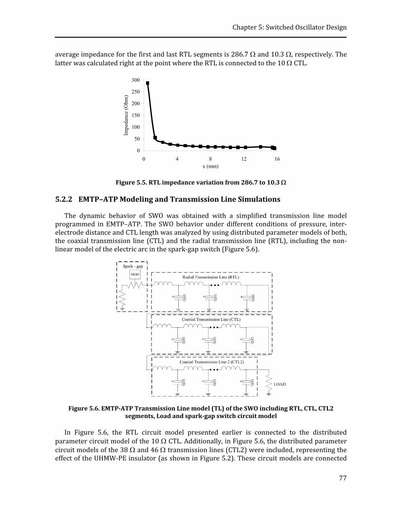
Chapter 5: Switched Oscillator Design
77
average impedance for the first and last RTL segments is 286.7 and 10.3 , respectively. The latter was calculated right at the point where the RTL is connected to the 10 CTL.
0
50
100
150
200
250
300
0 4 8 12 16x (mm)
Impe
danc
e (O
hm)
Figure 5.5. RTL impedance variation from 286.7 to 10.3
5.2.2 EMTP–ATP Modeling and Transmission Line Simulations
The dynamic behavior of SWO was obtained with a simplified transmission line model programmed in EMTP–ATP. The SWO behavior under different conditions of pressure, inter‐electrode distance and CTL length was analyzed by using distributed parameter models of both, the coaxial transmission line (CTL) and the radial transmission line (RTL), including the non‐linear model of the electric arc in the spark‐gap switch (Figure 5.6).
Figure 5.6. EMTPATP Transmission Line model (TL) of the SWO including RTL, CTL, CTL2 segments, Load and sparkgap switch circuit model
In Figure 5.6, the RTL circuit model presented earlier is connected to the distributed
parameter circuit model of the 10 CTL. Additionally, in Figure 5.6, the distributed parameter circuit models of the 38 and 46 transmission lines (CTL2) were included, representing the effect of the UHMW‐PE insulator (as shown in Figure 5.2). These circuit models are connected

Chapter 5: Switched Oscillator Design
78
to a 100 resistor that simulates the load impedance (LOAD). Note that the transmission lines are charged with a voltage equal to the breakdown voltage.
In the SWO Transmission Line model (TL) of Figure 5.6 the arc‐resistance (Rarc) proposed in chapter 4 was included, together with the arc‐inductance (Larc), which in this case was estimated as a constant value of 1 nH. Figure 5.7 shows the simulated output current waveform for SF6 at 1000 kPa and d = 0.5 mm. The CTL length is L = 183 mm.
Figure 5.7. Waveform of the SWO from the TL simulation for SF6 at 1000 kPa and d = 0.5 mm
5.3 Effect of the Geometrical Parameters on the SWO Generated Signals
In this section, the effects of the spark‐gap switch pressure p, inter‐electrode distance d and Coaxial Transmission line length L on the SWO generated current signals are evaluated. The inner and outer diameters are shown in Figure 5.2. Table 5.2 summarizes the parameters and their selected values.
Table 5.2. Variable geometrical and physical parameters of the SWO
Parameter Values Unit
Gas SF6 ‐‐‐‐ Inter‐electrode distance (d) 0.25, 0.5, 0.75, 1 mm Pressure (p) 400, 600, 800, 1000 kPa Coaxial Transmission Line length (L) 20, 70, 126, 183 mm
5.3.1 Safety factor (S)
The maximum charging voltage on the SWO transmission line depends on the spark–gap switch breakdown voltage VB, which is a function of pd. Therefore, for a constant pressure p, a higher charging voltage is achieved by increasing d. However, an excessive increase in d can cause the discharge to occur at any point in the CTL and not at the center of the RTL, as desired.
As the discharge location is extremely relevant to the SWO operation, a control measure to avoid an operational system failure should be incorporated. The safety factor (S) introduced in

Chapter 5: Switched Oscillator Design
79
(Armanious et al., 2010) is defined as the ratio between the static electric field at the spark–gap switch center (EM) and the static electric field at the CTL inner conductor (ECTL).
CTL
M
E
ES (5.7)
The factor S for the four inter‐electrode distances described in Table 5.2, under standard
atmospheric conditions was calculated using a COMSOL electrostatic simulation. Figure 5.8 shows the relation between S and d. In all cases the safety factor is greater than 1, which ensures that discharge occurs at the desired location.
1
1,1
1,2
1,3
1,4
1,5
1,6
1,7
1,8
0,2 0,4 0,6 0,8 1
inter-electrode distance d (mm)
Saf
ety
Fac
tor
S
Figure 5.8. Safety factor S vs. the interelectrode distance d for distance values between 0.25 and 1 mm under atmospheric conditions, evaluated using COMSOL simulations
5.3.2 Coaxial Transmission Line Length (L)
In this section, the influence of the CTL length L on the resonance frequency (f0) and the Q – factor (Q) is analyzed. The SWO selected conditions are: constant pressure of 1000 kPa and inter‐electrode distance d equal to 1 mm.
Figure 5.9. Power spectrum for different values of CTL length (L) using the TL simulation results for SF6 at 1000 kPa and d = 1 mm
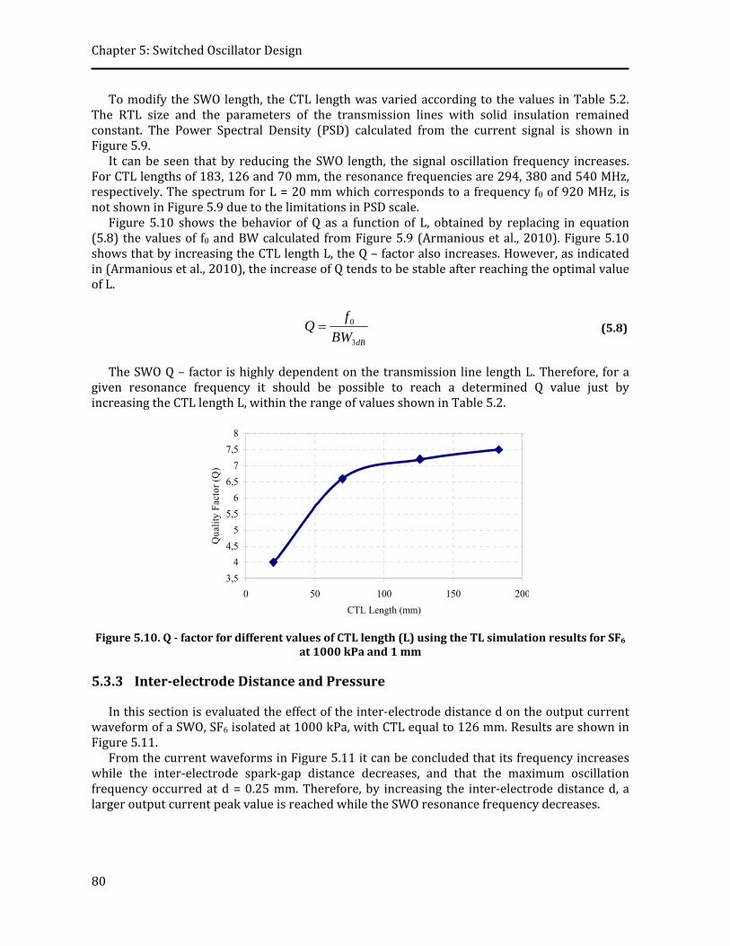
Chapter 5: Switched Oscillator Design
80
To modify the SWO length, the CTL length was varied according to the values in Table 5.2. The RTL size and the parameters of the transmission lines with solid insulation remained constant. The Power Spectral Density (PSD) calculated from the current signal is shown in Figure 5.9.
It can be seen that by reducing the SWO length, the signal oscillation frequency increases. For CTL lengths of 183, 126 and 70 mm, the resonance frequencies are 294, 380 and 540 MHz, respectively. The spectrum for L = 20 mm which corresponds to a frequency f0 of 920 MHz, is not shown in Figure 5.9 due to the limitations in PSD scale.
Figure 5.10 shows the behavior of Q as a function of L, obtained by replacing in equation (5.8) the values of f0 and BW calculated from Figure 5.9 (Armanious et al., 2010). Figure 5.10 shows that by increasing the CTL length L, the Q – factor also increases. However, as indicated in (Armanious et al., 2010), the increase of Q tends to be stable after reaching the optimal value of L.
dBBW
fQ
3
0 (5.8)
The SWO Q – factor is highly dependent on the transmission line length L. Therefore, for a
given resonance frequency it should be possible to reach a determined Q value just by increasing the CTL length L, within the range of values shown in Table 5.2.
3,5
4
4,5
5
5,5
6
6,5
7
7,5
8
0 50 100 150 200
CTL Length (mm)
Qua
lity
Fac
tor
(Q)
Figure 5.10. Q factor for different values of CTL length (L) using the TL simulation results for SF6 at 1000 kPa and 1 mm
5.3.3 Interelectrode Distance and Pressure
In this section is evaluated the effect of the inter‐electrode distance d on the output current waveform of a SWO, SF6 isolated at 1000 kPa, with CTL equal to 126 mm. Results are shown in Figure 5.11.
From the current waveforms in Figure 5.11 it can be concluded that its frequency increases while the inter‐electrode spark‐gap distance decreases, and that the maximum oscillation frequency occurred at d = 0.25 mm. Therefore, by increasing the inter‐electrode distance d, a larger output current peak value is reached while the SWO resonance frequency decreases.

Chapter 5: Switched Oscillator Design
81
Figure 5.11. Current waveforms of a SWO, SF6 isolated at 1000 kPa with a 126 mm long CTL, from the TL simulations. Results are shown for four interelectrode distances
Figure 5.12 shows the variation of the resonance frequency (f0) and the 3 dB bandwidth
(BW3dB) as a function of d.
350
360
370
380
390
400
410
420
430
0,25 0,5 0,75 1inter-electrode distance d (mm)
Res
onan
ce F
requ
ency
(M
Hz)
44
46
48
50
52
54
56
58
60
Ban
dwid
th a
t 3 d
B (
MH
z)
BW
f0
Figure 5.12. Resonance frequency and 3 dB bandwidth for different interelectrode distances obtained from the TL simulations of a SWO, SF6 isolated at 1000 kPa with a 126 mm long CTL Results on Figure 5.12 and equation (5.8) were used to evaluate the relationship between d
and Q shown in Figure 5.13. Results in Figure 5.13 show that for a constant pressure p, Q is an almost‐constant for
different values of d. This means that by changing d, both the resonance frequency (f0) and the 3 dB bandwidth (BW3dB), change almost at the same rate, while Q remains approximately constant (Armanious et al., 2010). Additionally, Figure 5.13 shows an important variation of Q with respect to pressure. This large variation of Q can be explained as follows: At lower pd values, the signal rise‐time increases (Schaefer et al., 1990). Thus, the output signal has more energy on the lower bands of the spectrum; this increases the 3 dB bandwidth (BW3dB), and therefore the largest amount of energy cannot be tuned at f0, causing a reduction in Q.
In summary, by increasing the inter‐electrode distance d, the current peak increases while both the resonance frequency and the Q ‐ factor decrease. Additionally, by increasing pressure, Q increases; and by changing the effective length of the SWO, f0 decreases.

Chapter 5: Switched Oscillator Design
82
5,0
5,5
6,0
6,5
7,0
7,5
8,0
0 0,2 0,4 0,6 0,8 1 1,2inter-electrode distance d (mm)
Qua
lity
fact
or Q
p = 400 kPa p = 600 kPap = 800 kPa p = 1000 kPa
Figure 5.13. Q – factor for different SF6 pressures vs. interelectrode distance (d) for a generator length L = 126 mm
5.4 Electromagnetic Model (EM)
The SWO electromagnetic model (EM) was analyzed with the computer program CST Microwave Studio. Figure 5.14 shows the normalized current on the load for d equal to 0.25, 0.5, 0.75 and 1 mm. The CST EM model uses an input file defined on a discrete port (1 μ resistive load), which contains data measured in the constructed generator using an adapted load (long transmission line). Four pulses (one for each d) were measured and used for the simulation.
The Electromagnetic simulations (EM) corroborated the results obtained with the Transmission Line simulations (TL): the maximum oscillation frequency was reached at d = 0.25 mm; moreover, the frequency decreases while the inter‐electrode distance increases.
Figure 5.14. Waveforms of a SWO, SF6 isolated at 1000 kPa with a 126 mm in length CTL, obtained with EM simulations. Results are shown for four different interelectrode distances
Figure 5.15 shows the PSD for the signals in Figure 5.14. For the inter‐electrode distances
0.25, 0.5, 0.75 and 1 mm, the resonance frequencies are 403, 379, 360 and 350 MHz, respectively.

Chapter 5: Switched Oscillator Design
83
Figure 5.15. Power spectrum for different interelectrode distances (d) from the EM simulation of a SWO, SF6 isolated at 1000 kPa with a 126 mmlong CTL
From Figure 5.15 and equation (5.8), the calculated values of the Q ‐ factor for d equal to
0.25, 0.5, 0.75 and 1 mm are 8.34, 8.23, 8.18 and 8, respectively. Figure 5.16 shows a comparison between the obtained PSD from the transmission line model
(TL) and the electromagnetic model (EM) for a SWO, SF6 isolated at 1000 kPa, with a 126 mm‐long CTL and d = 0.5 mm.
The waveforms obtained from TL model and those from the EM model show a similar behavior. However, there are some differences: the respective resonance frequencies given by the TL‐ and the EM‐models were 400 MHz and around 379 MHz, while the respective resulting bandwidths were 54 MHz and 46 MHz. Therefore, from equation (5.8) the calculated Q value in the EM model is a little higher than that obtained with the TL model.
Although the SWO TL model included most of the geometric variations and materials in each segment, just a 5% difference between the models was obtained. These differences could be explained by the approximations made during the EMTP‐ATP simulation process. Therefore, due to the small differences, approximated values of f0, BW3dB and Q can be obtained with any of the two developed models.
Figure 5.16. Comparison of the Power Spectrum Density obtained with the TL and the EM models of a SWO, SF6 isolated at 1000 kPa, with a 126 mmlong CTL and d = 0.5 mm

Chapter 5: Switched Oscillator Design
84
5.5 Testing of the SWO
In this section some laboratory test results of a 100 transmission line SWO terminated in a 100 resistor, are presented. Figure 5.17 shows the constructed generator and its main parts, namely the CTL inner and outer conductors, the bottom housing, the insulating cap and the ground plane. The main parameters of the constructed SWO are the following: CTL length L = 126 mm, inter‐electrode distance d = 0.25 mm, inner conductor diameter = 29.66 mm, outer conductor diameter = 35.04 mm, ground plane diameter = 0.3 mm, dielectric material: UHMW‐PE, r = 2.3 and maximum pressure = 1500 kPa. Under these conditions, the expected f0, BW3dB and Q were 425 MHz, 57 MHz and 7.4, respectively.
Figure 5.17. Constructed SWO. Coaxial transmission line conductors, electrode, bottom housing, ground plane and insulating cap
5.5.1 Experimental Setup
The constructed SWO was tested using a coaxial transmission line with Z0 = 100 , terminated in a 100 coaxial resistor (LOAD). This setup is shown in Figure 5.18, where a blocking capacitor (C) that filters DC current through the load was connected between the SWO and the load (Giri et al., 2010). This capacitor was selected so as to obtain a low impedance value with respect to the load impedance right at the center of the working band (425 MHz). In this case, the loading effect on the HV source was considered, so the time constant associated to the blocking capacitor and the load was selected to be low with respect to the time constant that governs the charging cycle of the generator (~ 333 pF), the selected value was 280 pF. This capacitor discharges through the load; however, it is not expected to change the dynamics of the oscillator although it might decrease the Q due to series losses.
Four ferrites, used to protect the source against high frequency signals, and a 50 M limiting resistor were connected between the 80 kV high voltage source and the inner conductor of the coaxial transmission line used in the tests. The derivative magnetic field sensor used to measure the signals is also shown in Figure 5.18. The signals were measured using a 1 GHz, 4 GSa/s oscilloscope (OSC).

Chapter 5: Switched Oscillator Design
85
Figure 5.18. Experimental Setup. SWO, coaxial transmission line, load, ground plane, small loop sensor, ferrites, blocking capacitor C and 50 M resistor R
5.5.2 Laboratory Tests
Four laboratory tests at different SF6 pressures (400, 600, 800 and 1000 kPa) were performed. As the parameters of interest are Q and ω0, the measured waveforms were normalized to their maximum values. In order to find ω0, the Power Spectrum Density (PSD), obtained by using the FFT, was normalized. Figure 5.19 shows an example of the 1000 kPa case, where the resonance frequency is 416 MHz.
Figure 5.19. Normalized measured output PSD of a SWO, SF6 isolated at 1000 kPa, with a 126 mm long CTL
The measured di/dt in time domain is shown in Figure 5.20, shaped by the exponential
envelope in order to obtain 0. From this figure, the exponential decaying factor (0) is 2.5x10⁸ [1/s]. Therefore, using equation (5.8) and 0 (2.61x10⁹ [rad/s]), obtained from Figure 5.19, the calculated Q is 5.23.
Figure 5.20 shows a comparison between experimental and simulated signals, including the blocking capacitor C. As a derivative sensor was used in these laboratory tests, simulated signals were derived so as to be compared with experimental results.

Chapter 5: Switched Oscillator Design
86
Figure 5.20. Normalized measured output signal in the time domain, compared with the derivative signal from EMTPATP and CST results
A similar behavior was observed during the first 9 ns; and, as described in section 5.4, a
difference of 5 % in the values of f0 and Q, obtained from any of the two developed models, was estimated. Comparing the experimental resonance frequency (416 MHz) with the one calculated from the TL and EM models (425 MHz and 408 MHz, respectively), it can be observed that the results obtained from the simulations fit well the laboratory test results. On the other hand, some differences were observed between the simulated Q (7.4 and 7.8) and the Q value obtained from the laboratory test (5.2).
These differences may be due to: 1) the existence of flaws in the SWO generator solid dielectric zone; 2) the fact that the coaxial load might not be a perfect 100 resistor, having a small reactive part which directly affects the Q ‐ factor; 3) losses in the transmission line conductors and losses in the blocking capacitor, which were not included in the simulation (this may reduce Q‐factor values and displace the resonance frequency); 4) errors associated with the signal sampling process to obtain the resonance frequency. Despite these differences, it can be stated that the experimental results validate the design methodology.

6 Conclusions
A Pulse Generator based on a coaxial transmission line and a self‐breaking spark‐gap charged with a D.C. voltage source was designed, built and tested. Laboratory tests, together with circuit‐(EMTP‐ATP), electrostatic‐(COMSOL) and electromagnetic‐(CST) simulations were developed. Empirical and theoretical equations were analyzed and compared with experimental results. A switching oscillator was developed based on some of the present research results. This experimental process allowed to fulfill the objective proposed at the beginning of the research “To study the dynamic behavior of the electrical discharge channel developed in a homogeneous electric field for different gases. Distances in the order of fractions of millimeter and some well defined pressures are considered”. In this chapter, the main conclusions of the thesis are summarized.
6.1 Pulse Generator
A design methodology for a pulse generator was presented in this thesis. The pulse generator design was based on theoretical and empirical criteria and it was supported by COMSOL simulations. The pulse generator was modeled and simulated using the EMTP‐ATP program. From this model, the effects of the D‐dot sensors location in the output signals were evaluated.
Rogoswki profile electrodes were designed and simulated with the electrostatic simulation program COMSOL. Simulations show that the designed electrodes do not affect the produced electric field.
2D axial‐symmetric simulations were performed using the Structural Mechanics module of COMSOL to determine if the walls of the pressurized chamber suffer any deformation due to the internal gas pressure. A maximum displacement of 5.31 m in the axial direction was observed, whereas the maximum variation in the radial direction was 1.3 m.
A process was developed to correct the inter‐electrode distance, based on a derived functional relation between displacement and pressure. The results in air and SF6 were reasonable and then, a corrected inter‐electrode distance was used in the present research work when referring to the inter‐electrode distance (d).
It was found that different charging voltage waveforms are recorded depending on the D‐dot position in the PFL with respect to the spark‐gap. A hypothesis was formulated claiming that this is because the sensor does not record all the charge moving along the transmission line. To confirm this hypothesis, both the charge stored up to the D‐dot sensor location and also the

Chapter 6: Conclusions
88
charge stored up until the spark‐gap were calculated on the basis of EMTP‐ATP simulations. Based on these calculations, the hypothesis was validated.
6.2 Experimental Results
Air, SF6 and argon show a linear increase in the breakdown voltage with respect to the pressure‐distance relation. This behavior is similar to the predicted by the theoretical and experimental models.
The measured derivative electric field waveforms showed a wave reflection returning from the outer boundary of the pulse generator where a 50 M limiting resistor is located. The position of D‐dot1 is such that these reflections were recorded around 2.3 ns after the spark‐gap breaks down. Based on that observation, the limit of useful breakdown information was 2.3 ns.
The effect of the high impedance boundary in the recorded waveforms was studied with an electromagnetic model implemented in CST. Simulation results corroborated that 2.3 ns after the spark‐gap breaks down the recorded waveforms were affected by the wave reflection returning from the outer boundary at the limiting resistor location.
The parameters selected to characterize the breakdown phenomenon were the breakdown voltage, the resistive phase time of the switching time, the Full Width at Half Maximum, and the arc‐resistance (Rarc). For the experimental conditions described in this thesis, SF6 shows the best switching performance.
To analyze the switching process, the resistive phase time was evaluated. Initially, the measuring system rise‐time and the inductive phase time were determined and then subtracted from the measured rise‐time to obtain R. In general, for the resistive time values a logarithmic decreasing trend was observed as the pd value increases,.
From measurements it is possible to affirm that the FWHM is almost a constant parameter which depends neither on the type of gas, nor on the pressure, nor on the inter‐electrode distance. This parameter depends only on both, the equivalent capacitance of the charge transmission line (PFL) and on the characteristic impedance of the transmission line (Z0).
The arc‐resistance is characterized by two stages: an initial stage and a quasi‐stationary stage. In the first stage a fast transition from some k up to tens of Ohms was observed, while the final stage has an almost flat behavior with a small variation in the arc‐resistance. Since a faster switch closure results in lower energy losses, SF6 would produce a more efficient switching.
Values of pulse repetition frequency between 0.3 and 16 kHz were recorded, depending on the pd value and the applied voltage. At lower pd values and higher charging voltages Vg, the bigger PRF.
Switching efficiencies between 0.8 and 0.9 were calculated by using two different equations. Based on the results, it is possible to affirm that for the gases and pd conditions used in this thesis, the most efficient switching process occurs in SF6.
6.3 Sparkgap Modeling
The electric field influence and the empirical constants were changed. In the case of argon at low pd values, some differences were observed between calculated and theoretical R values. It appears that the resistive phase time does not increase by increasing pressure. Therefore, in the

Chapter 6: Conclusions
89
case of argon the proposed equations overstate the influence of pressure (or gas density) or understate the electric field influence on the resistive phase time.
The arc‐resistance results obtained from laboratory tests were compared with the most accepted models (Toepler, Vlastos, Sorensen et al. and Kushner et al.). Arc‐resistance model given by Kushner et al. showed the best results for the total time period considered in this investigation: 2.3 ns. Additionally, a new constant of proportionality for Kushner´s equation was proposed. This constant corresponds to the relation between the pressure reduced electric field at breakdown E/p, times the inter‐electrode distance d: (d*E/p). The proposed equation takes in account the type of gas, the pressure and the inter‐electrode distance and it can be easily calculated for any self‐breakdown switch working in the pd range described in this investigation. In the case of argon, important differences were observed between the new equation and the experimental results.
For the maximum value of PRF recorded (16 kHz) the time between pulses was 63 s, which is much lower than that the time that the voltage recovery processes requires. Therefore, the gas was not fully recovered when a new spark broke down the spark‐gap. As a consequence, the voltage level at which a subsequent discharges occurred was lower than the static breakdown voltage.
The empirical model proposed in this thesis to estimate the PRF in air reproduces the experimental results with a maximum error of 15 %.
Finally, in this investigation an improved spark‐gap model was proposed. This new model includes the arc‐resistance model proposed in this investigation and a constant series arc‐inductance of 6 nH. Simulated and experimentally obtained waveforms fit well. However, some differences in the pulse duration were observed, meaning that the equivalent capacitance of the constructed PFL was higher than the one used in the simulations. This difference was overcome by adding an additional 1 pF capacitance, which was the parasitic capacitance between the outer conductor of the PFL and the limiting resistor. This additional capacitance was observed and calculated in a COMSOL electrostatic simulation of the complete generator.
An EMTP‐ATP generator model including the parasitic capacitance was developed and tested. An excellent agreement between the simulated and experimental waveforms was obtained. Despite some small differences, it is possible to affirm that measurements and simulations agree. From the experimental results and models presented in this investigation, it can be concluded that the constructed generators can be used in the understanding of sub‐nanosecond gas discharges in sub‐millimeter spark‐gaps. Additionally, the described design and simulation methodology can be used to design and construct new pulse generators for different applications.
6.4 Switching Oscillator
A SWO design methodology was presented. Based on the previous results the SWO was modeled and simulated using EMTP‐ATP. From this model, the effects of the generator length, inter‐electrode distance and pressure over the SWO resonance frequency, bandwidth and Q ‐ factor were evaluated.
It was found that if the SWO length increases, so does the Q ‐ factor; however, the resonance frequency decreases. By changing the inter‐electrode distance, both the resonance frequency and the bandwidth change at almost the same rate, maintaining an approximately constant Q ‐ factor.
A good correlation was observed between the results obtained with the CST Microwave Studio (an electromagnetic model) and the EMTP‐ATP (a transmission line model). However,
Chapter 6: Conclusions
90
the TL model has some advantages over the EM model, such as the spark‐gap switch arc model that was included in the EMTP–ATP model, the easy implementation and low computational cost in terms of simulation time and required memory. Additionally, the TL model allows an easy modification of the design.
A SWO was designed and constructed based on the proposed methodology, and tested in laboratory. The resonance frequency from simulations fit well with the laboratory test results.
There is concern about the calculated Q ‐ factor from laboratory tests, since there are some mismatches between different parts of the system that could not be included in the simulation models. However, it is possible to affirm that in general, measurements and simulations agree. Therefore, experimental results validate the design methodology.
6.5 Final Remarks
The simulations performed to determine if the walls of the pressurized chamber suffer any deformation due to the internal gas pressure should be improved. The mechanical properties of the UHMW‐PE, including the Young’s module, Poisson’s ratio and density must be accurately determined to be included in the simulations.
Ideally, the transit time of an electromagnetic pulse through a spark‐gap filled with gas at high pressure depends on the inter‐electrode distance and the insulating gas type. However, for a spark‐gap inserted into a coaxial transmission line, the achievable rise‐time is determined by the spark‐gap closure and the re‐establishment of the propagating electric field in the region between the inner and outer conductors of the coaxial transmission line. In this thesis the distance between the inner and outer conductors was large enough (38.75 mm) to ensure the voltage hold‐off in the coaxial system. As the breakdown voltage is inversely proportional to the inner radius and the logarithm of the radius ratio, in a further work for a given impedance, e.g. 100 , the inner conductor radius should be chosen to be small.
The pressurized chamber design must be improved. Other materials should be studied to ensure that there are not changes in the inter‐electrode distance due to the pressure inside the chamber. The best option could be the use of a complete pressurized generator without insulated materials along the transmission lines.
The new constant of proportionality proposed for the equation of Kushner must be checked using a larger variety of gases over wider pd ranges.
Despite the good agreement between measurements and simulation results, there are some mismatches between different parts of the system that could not be included in the simulation models. Therefore, an improved transmission line model should be implemented including these mismatches. However, an electromagnetic model, including the arc‐channel model would be a good choice to take into account the effects of the different transmission lines systems and materials in the propagating wave.

Acknowledgements
I want to express my thanks to Professor Francisco Román for his guidance and support during my doctoral studies and before of them. I really appreciate the opportunity he gave me to be part of the EMC‐UNC Group during almost nine years.
Cattleya Project and its supporting companies are greatly acknowledged for their financial grants without which this research would not be possible.
I would like to thank all my friends and colleagues from the Electromagnetic Compatibility Research Group for their help.
Special thanks are due to Mario Echeverri, who worked with me in the development process of the SWO. The effort and dedication have paid off.
I would also like to express my thanks to Professor Farhad Rachidi, from EPFL, Switzerland, who welcomed me at the EMC‐lab.
Finally, I would like to thank my wife Olguita for always having the time to listen to my hypothesis and theories, for reading my thesis, for the invaluable comments and especially for the patience.

References Agee, F J., C. E. Baum, W.D. Prather, J.M. Lehr, P. O’Loughlin, Jon S. H. Schoenberg, D.W. Scholfield, R.J. Torres, J.P. Hull, J.A. Gaudet, UltraWideband Transmitter Research, IEEE Trans. Plasma Sci., vol 26, 860–873 (1998). Agilent Technologies, Understanding Oscilloscope Frequency Response and Its Effect on RiseTime Accuracy, Application Note 1420 (2002). [on line], available in: http://cp.literature.agilent.com Agilent Technologies, Bandwidth and Rise Time Requirements for Making Accurate Oscilloscope Measurements, Application Note (2012). [on line], available: http://cp.literature.agilent.com Akiyama, H., M. Kristiansen, H. Krompholz, B. Maas, Currentvoltage characteristics of a highcurrent pulsed discharge in air, IEEE trans. on plasma science, vol. 16, no. 2, 312–316 (1988). Armanious, M., J.S. Tyo, M. Skipper, M.D. Abdalla, W.D. Prather, J.E. Lawrence, Interaction between geometric parameters and output waveforms in high power quarterwave oscillators, IEEE Trans. Plasma Sci., vol 38, no. 5, 1124–1131 (2010). Baum, C.E., E.L. Breen, J.C. Giles, J. O’neill, G.D. Sower, Sensors for electromagnetic pulse measurements both inside and away from the nuclear source regions, IEEE transactions on antennas and propagation, vol. AP‐26, no. 1, 22–35 (1978). Baum, C.E., Sensors for measurement of intense electromagnetic pulses, Proceedings of the 3rd IEEE Pulsed Power Conference, 179–185 (1981). Baum, C.E., Switched oscillators, CESDN, Note 45 (2000). [on line], available in: http://ece.unm.edu/summa/notes Baum, C.E., Antennas for the switched oscillator source, SSN, Note 455 (2001). [on line], available in: http://ece.unm.edu/summa/notes Bluhm, H., Pulsed Power Systems. Principles and Applications. 1‐27, First edition, Springer, Power Systems Collection, Germany (2006).
References
93
Braginskii, S. I., Theory of the development of a spark channel, Sov. Phys.—JETP, vol. 34, no. 7, 1068–1074 (1958). Carboni, V., H. Lackner, D.V. Giri, J. Lehr, The breakdown fields and risetimes of selected gases under conditions of fast charging (~20 ns and less) and high pressures (20 – 100 atmospheres), Switching notes ‐ SwN32 (2002). [on line], available in: http://www.ece.unm.edu/summa/notes/ Cary, Jr., W.K., D.D. Lindberg, J.W. Rice, Breakdown in small, flowing gas spark gaps, Proceedings of the 2nd IEEE Pulsed Power Conference, 114–118 (1979). Christophorou, L.G., D.L. McCorkle, S.R. Hunter, Gas Mixtures for Spark Gap Closing Switches with Emphasis on Efficiency of Operation, Gaseous Dielectrics, vol. 5, 381–388 (1987). Diaz, O., Design and Construction of a Fast Impulse Current Generator Based on the Floating Electrode Principle, Master of Science thesis, Universidad Nacional de Colombia (2005). Diaz, O., F. Roman, A new fast impulse current generator based on the floating electrode properties, Proc. of the 14th International Symposium on High Voltage Engineering (2005‐1). Diaz, O., F. Roman, Spark Gap Behavior in a Compact Electrostatic Fast Impulse Current Generator, Proc. of the 8th International Symposium on Lightning Protection, SIPDA (2005‐2). Diaz, O., F. Roman, Design and construction of a compact electrostatic fast impulse generator, Proc. of the 15th IEEE Pulsed Power Conference, 771–774 (2005‐3). Diaz, O., F. Roman, Improvement of the output current response of an electrostatic fast impulse current generator, Proc. of the 28th International Conference on Lightning Protection (2006). Diaz, O., L. Arevalo, F. Roman, Understanding the corona space charge influence on the ESDlike discharge produced by a floating electrode in a fast impulse current generator, Proc. of the 9th International Symposium on Lightning Protection, SIPDA (2007). Dick, A., S. Macgregor, M. Buttram, R. Pate, L. Rinehart, K. Prestwich, Breakdown Phenomena in UltraFast Plasma Closing Switches, IEEE Transactions on Plasma Science, vol. 28, issue 5, 1456–1462 (2000). Dick, A., S. Macgregor, R. Pate, Transmission line switch design for the investigation of subnanosecond electrical breakdown, Meas. Sci. Technol., 13, 539–546 (2002). Donaldson, A.L., M. Kristiansen, M. Hagler, G. Jackson, L. Hatfield, Electrode erosion in a high energy spark gap. Proceedings of the 4th IEEE Pulsed Power Conference, 530–533 (1983). Edgel, W.R., I vs. Idot, Application Note 890, Prodyn Technologies (1990‐1). [on line], available in: http://www.prodyntech.com/download/appnotes/ Edgel, W.R., Electric and magnetic field sensor application. (A way to get from Maxwell’s equations to field measurements), Application Note 192, Prodyn Technologies (1990‐2). [on line], available in: http://www.prodyntech.com/download/appnotes/

References
94
Engel, T., A. Donaldson, M. Kristiansen, The pulsed discharge arc resistance and its functional behavior, IEEE transactions on plasma science, vol. 17, no. 2, 323–329 (1989). Fletcher, R.C., Impulse breakdown in the 109 sec range of air at atmospheric pressure, Physical Review, vol. 76, issue 10, 1501–1511 (1949). Giao, T., Electrode Design for Testing in Uniform Field Gaps, IEEE Transactions on Power Apparatus and Systems, vol. PAS‐99, no. 3, 1235–1242 (1980). Giri, D.V., F.M. Tesche, M.D. Abdalla, M.C. Skipper and M. Nyffeler, Switched oscillators and their integration into helical antennas, IEEE Trans. Plasma Sci., vol 38, no. 5, 1124–1131 (2010). Gratton, R., S. Mangioni, J. Niedbalski, R. Valent, “Inductance and resistance of a small pressurized spark gap for Blumleindriven nitrogen”, Journal of Physics E: Sci. Instrum., vol. 21, 851–853 (1988). Greason, W.D., Methodology to study the resistance of spark discharges, IEEE Transactions on industry applications, vol. 35, no. 2, 359–365 (1999). Heeren, T., J.T. Camp, J.F. Kolb, K.H. Schoenbach, 250 kV subnanosecond pulse generator with adjustable pulsewidth, IEEE transactions on dielectrics and electrical insulation, vol. 14, no. 4, 884–888 (2007). Heylen, A., Sparking Formula for Very High–Voltage Paschen Characteristics of Gases, IEEE Trans. Elec. Insul. Magazine, vol. 2, 25–35 (2006). Istenic, M., I. Smith, B. Novac, Dynamic resistance calculation of nanosecond sparkgaps, Proceedings of the 15th IEEE Pulsed Power Conference, 608–611 (2005). Kawaguchi, Y., K. Sakata, S. Menju, Dielectric Breakdown of Sulphur Hexafluoride in Nearly Uniform Fields, IEEE Trans. Power Apparatus and Systems, vol. PAS‐90, Issue 3, 1072–1078 (1971). Kind, D., H. Karner, High Voltage Insulation Technology, 1‐22, Vieweg, Germany (1985). Kuffel, E., W.S. Zaengl, J. Kuffel, High Voltage Engineering, 281‐360, 2nd Edition, Newnes, Breat Britain (2000). Kushner, M.J., W.D. Kimura, S.R. Byron, arc resistance of lasertriggered spark gaps, Journal of Applied physics, vol. 58, no. 5, 1744 – 1751 (1985). Lehr, J.M., C.E. Baum, W.D. Prather, F.J. Agee, Aspects of ultrafast spark gap switching for UWB HPM generation, Proceedings of the 11th IEEE Pulsed Power Conference, vol. 2, 1033–1041 (1997). Liu, Z., A.J. Pemen, R.T. van Hoppe, G.J. Winands, E.J. van Heesch, K. Yan, An Efficient, Repetitive Nanosecond Pulsed Power Generator with Ten Synchronized Spark Gap Switches, IEEE Trans. on Dielectrics and Electrical Insulation, vol. 16, no. 4, 918‐925 (2009).

References
95
MacGregor S.J., S.M. Turnbull, F.A. Tuema, A. Phelps, Methods of Improving the Pulse Repetition Frequency of High Pressure Gas Switches, 10th IEEE Int. Pulsed Power Conf. 249‐254 (1995). MacGregor, S.J., S.M. Turnbull, F.A. Tuema, O. Farish, Factors Affecting and Methods of Improving the Pulse Repetition Frequency of Pulse‐Charged and DC‐Charged High‐Pressure Gas Switches, IEEE Transactions on Plasma Science, vol. 25, no. 2, 110‐117 (1997). Malik, N.H., A.H. Qureshi, Breakdown Mechanisms in SulphurHexafluoride, IEEE Trans. Electr. Insulation, vol. EI‐13, no. 3, 135–45 (1987). Mankowski, J., M. Kristiansen, A Review of Short Pulse Generator Technology, IEEE Trans. Plasma Sci., vol. 28, 102–108 (2000). Martin, J.C., Duration of the resistive phase and inductance of spark channels, Switching notes ‐ SwN9 (1965). [on line], available in: http://www.ece.unm.edu/summa/notes/ Martin, J.C., Nanosecond pulse techniques. Proceedings of the IEEE Pulsed Power Conference, vol. 80, issue 6, 934–945 (1992). Martin, T., A. Guenther, M. Kristiansen (editors), J.C. Martin on Pulsed Power. Plenum Press, Advances in Pulsed Power Technology, volume 3 (1996). Montaño, R., M. Becerra, V. Cooray, M. Rahman, P. Liyanage, resistance of spark channels, IEEE Trans. on plasma science, vol. 34, no. 5, 1610–1619 (2006). Mora, N., Electrical model of the Roman Generator, Master of Science thesis, Universidad Nacional de Colombia (2009). Mora, N., F. Vega, F. Roman, N. Peña, F. Rachidi, Corona Charged subnanosecond impulse generator, Proc. of the EMC Zurich 2009 conference (2009‐1). Mora, N., F. Vega, F. Roman, Application of Electrical Coronas in Fast Impulse Generation, Proc. of the IEEE CREES (2009‐2). Moran, S.L., L.W. Hardesty, High–Repetition Rate Hydrogen Spark Gap, IEEE Trans. Electron Device, vol. 38, 726–730 (1991). Naidu, M.S., V. Kamaraju, High Voltage Engineering, 12‐39, 2nd Edition, McGraw‐Hill, USA (1996). Nasser, E., Fundamentals of Gaseous Ionization and Plasma Electronics, Wiley‐Interscience, Wiley Series in Plasma Physics, USA (1971). Nunnally, W.C., Critical component requirements for compact pulse power system architectures, IEEE Transactions on plasma science, vol. 33, no, 4, 1262–1267 (2005). Pearson, J., J. Harrison, A uniform field electrode for use in a discharge chamber of restricted size: design and performance, Brit. J. Appl. Phys. (J. Phys. D), ser. 2, vol. 2, 77–84 (1969).

References
96
Pécastaing, L., J. Paillol, A. Gilbert, P. Domens, Design and Performance of High Voltage Pulse Generators for UltraWideband Applications, Meas. Sci. Technol. 12, 1718‐1725 (2001). Pommerenke, D., ESD: transient fields, arc simulation and risetime limit. Journal of Electrostatics, vol. 36, issue 1, 31–54 (1995). Prowse, W., J. Clark, UltraHighFrequency Gas Breakdown between Rogowski Electrodes, Proc. Phys. Soc., vol. 72, Issue 4, 625‐634 (1958). Rahaman, H., Investigation of a High–Power, High–Pressure Spark Gap Switch with High Repetition Rate, PhD Thesis, Universitat Erlangen, Nurnberg‐Germany (2007). Roman, F., Effects of Electric Field Impulses Produced by Electrically Floating Electrodes on the Corona Space Charge Generation and on the Breakdown Voltage of Complex Gaps, PhD Thesis dissertation, Faculty of Science and Technology, Uppsala University (1996). Roman, F., A repetitive and constant energy impulse current generator, U.S. Patent number 5. 923. 130 (1999). Roman, F., R. Montaño, V. Cooray, Varistor response under subsequent strokelike impulse current, Proc. of the 13th International Symposium on High Voltage Engineering (2003). Roman, F., N. Peña, J. Herrera, F. Santamaria, N. Mora, E. Aguilera, O. Diaz, F. Vega, Radiating broadband pulse generator with corona charging mechanism, Proc. of the EUROEM 2008 conference (2008) Schaefer, G., M. Kristiansen, A. Guenther (editors), Gas Discharge Closing Switches, Plenum Press, Advances in Pulsed Power Technology, volume 2, USA (1990). Scott, J.C., A.W. Palmer, Pressure dependence of the rise time of lasertriggered spark gaps, Journal of Phys. E: Sci. Instrum., vol. 11, 495‐496 (1978). Sorensen, T. P., M. Ristic, Rise time and timedependent sparkgap resistance in nitrogen and helium, Journal of Applied physics, vol. 48, no 1, 114–117 (1977). Vega, F., F. Rachidi, N. Peña, F. Roman, A Design of a Mesoband High Power Electromagnetic Radiator Using a Switched Oscillator and a corona Current Generator, Proc. of the URSI Conference (2008). Vega, F., N. Mora, F. Roman, N. Peña, F. Rachidi, B. Daout, Design and Construction of a Corona Charged High Power Impulse Generator, Proc. of the 17th IEEE Pulsed Power Conf. (2009). Vega, F., Design of a high power ultra wideband system using a fast impulse Current generator, PhD Thesis dissertation, Universidad Nacional de Colombia (2011). Verma, R., A. Shyam, S. Chaturvedi, R. Kumar, D. Lathi, P. Sarkar, V. Chaudhary, R. Shukla, K. Debnath, S. Sharma, J. Sonara, K. Shah, B. Adhikary, T. Jigna, J. Piyush, Impulse Electromagnetic Interference Generator, Proc. of the 26th IEEE Power Modulator Conference, 543–546 (2004).

References
97
Vlastos, A. E., The resistance of sparks, Journal of Applied physics, vol. 43, no. 4, 1986–1989 (1972). Wang, X., H. Luo, Y. Hu, Numerical simulation of the gas discharge in a gas peaking switch, IEEE Transactions on plasma science, vol. 35, no. 3, 702–708 (2007). Yan, K., E. Van Heesch, S. Nair, A. Pemen, A Triggered SparkGap Switch for HighRepetition rate HighVoltage Pulse Generation, Journal of Electrostatics, vol. 57, Issue 1, 29–33 (2003). Yin, Y., J. Liu, H. Zhong, J. Fenf, Experimental study of the recovery times of spark gap switch with different gases. Plasma science and technology, vol. 10, no. 3, 379–382 (2008).

Papers Santamaria, F., M. Echeverri, F. Roman, N. Peña, Switched Oscillator: Parameter Effects on the Generated Signals, IEEE Trans. on Plasma Science, vol. 40, issue 12 (2012). Santamaria, F., F. Roman, Design and Performance Analysis of a Subnanosecond Pulse Generator, IEEE Trans. on Plasma Science, submitted for publication (2012). Santamaria, F., F. Roman, Experimental Study of a Submillimeter Sparkgap, IEEE Trans. on Plasma Science, submitted for publication (2012). Santamaria, F., M. Echeverri, F. Roman, N. Peña, Geometric Parameters Influence on the Output Signals of Switched Oscillators, proceedings of the 4th Euro‐Asian Pulsed Power Conference EAPPC (2012). Santamaria, F., M. Echeverri, F. Roman, N. Peña, Geometric Parameters Influence on the Output Signals of Switched Oscillators, IEEE Trans. on Plasma Science, submitted for publication (2012).

99
Appendix 1: UHMW_PE Properties
Complete information about the UHMW‐PE properties is presented in next table. The information contained herein are typical values given by manufacturers but could change depending on several aspects.
Table A.1. UHMWPE Properties
Property Test Method Units Value Physical Density ASTM D‐792 kg/m3 930 Water absorption ASTM D‐570 % < 0.01 Mechanical Yield point ASTM D‐638 MPa 20 Elongation at yield ASTM D‐638 % 15 Tensile break ASTM D‐638 MPa 40 Elongation at break ASTM D‐638 % 250 Young’s modulus ASTM D‐638 MPa 830 Poisson’s ratio 0.46 Flexural modulus ASTM D‐790 MPa 758 Izod impact ASTM D‐4020 m_kPa 71.4 Compressive modulus ASTM D‐695 MPa 536 Compressive deformation ASTM D‐621 % at 6.9 MPa 6 – 8 Thermal Melt point ASTM D‐3417 ºC 137 – 143 Maximum operating temp. ºC 82 Electrical Volume resistivity ASTM D‐257 _m >10E13 Surface resistivity ASTM D‐257 >10E15 Dielectric constant at 60 Hz ASTM D‐150 2.3 Dielectric constant at 1 kHz ASTM D‐150 2.3 Dielectric constant at 1 MHz ASTM D‐150 2.3

Appendix 2: DDot Sensors
In this appendix, the sensors used to determine the spark‐gap voltage and their operation mode are described. Next, from the output voltage of the sensors, the equation needed to determine the voltages before and after the spark‐gap (V1 and V2) are presented.
The equivalent electric circuit and transfer function of the derivative electric field sensors are presented in (Edgel, 1990‐2) and described below.
Figure A.1. Ddot equivalent circuit where AEQ is the equivalent area of the sensor, D the electric field density, C and R the capacitance and output resistance of the sensor respectively, and V is the output voltage of the sensor. The differential equation representing the current though the circuit is:
R
VVC
R
V
dt
dVCDAi EQ
(A.1)
The equation in the s domain is given by:
R
sVsVsCsDsAEQ .... (A.2)
Solving the equation (A.2) for the output voltage:
1
..
RCs
RsDsAsV EQ (A.3)
DAi EQC
R V

Appendix 2: D‐dot Sensors
101
The response of these sensors can be divided in two parts, the first one is the low frequency response (differential mode), and the second one is the high frequency response (self integrating mode). In low frequency 1RC , then equation (A.3) reduces to:
sDsRAsV EQ ... (A.4)
Transforming back to the time domain:
DRAtV EQ (A.5)
In high frequency 1RC , then equation (A.3) reduces to:
C
sDAsV EQ (A.6)
Transforming back to the time domain:
C
DAtV EQ (A.7)
Therefore, depending of the operating frequency of the sensors, the equation (A.5) or the
equation (A.7) should be employed. However, when the signal frequency is high enough that (A.5) is not valid, but not high enough to use (A.7), which means that it is close to the cutoff frequency (fc), the sensor is operating in the transitional mode. In this mode, the full transfer function presented in (A.3) must be used.
The maximum operating frequency in this thesis is 1.4 GHz, and then the operating mode of the sensors should be verified at this frequency.
FD-5A D-dot Sensor Sensitivity
Ep = 1.67x10^3 V/m
0,0
0,1
0,2
0,3
0,4
0,5
0,6
0,7
0 5000 10000 15000 20000 25000 30000f, MHz
Vo
, V
olt
s
Vop' AeqD-dotR' Aeq D/C)
Figure A.2. Ddot calibration curve

Appendix 2: D‐dot Sensors
102
Figure A.2 shows the calibration curve of the sensors provided by the manufacturer for a homogeneous and constant electric field of 1.67 kV/m. The blue line is the actual response of the sensor; the red line is the low frequency approximation (Equation (A.4)) and the black line is the high frequency approximation corresponding to (Equation (A.4)).
From the figure, the cutoff frequency (fc) is 10 GHz and then, it is possible to use the low frequency approximation for which the output voltage is proportional to the first time derivative of the electric field density, the output resistance (R) and the equivalent area (AEQ). Then, from these measures the voltage on the transmission lines can be found. Solving the equation (A.5):
dttVRA
tDEQ
.1
(A.8)
Using the definition ED 0 , and rewriting:
dttVRA
tEEQ
.1
0 (A.9)
On the other hand, the voltage in a coaxial geometry as a function of the electric field strength is:
a
btEtV rAB ln (A.10)
where a and b are geometrical parameters described in chapter 2. Replacing the equation (A.9) in equation (A.10) and substituting the constants:
dttVtVAB .1011.1 13 (A.11)
This corresponds to the relationship between the D‐dot sensor output voltage (V) and the voltage across the transmission lines (VAB) presented in equation (2.22).

103
Appendix 3: Analog Voltmeter Verification
To determine the correct operation of the analog voltmeter used in the DC voltage measurements, a verification process was carried and it was described in section 2.3.2. In this appendix, the recorded voltages, its average values and the corresponding errors in the two voltage ranges are shown, where Vref is the voltage recorded with the high voltage probe in [kV], Vm is the voltage recorded with the analog voltmeter in [kV] and the error in [%].
Table A.2. DC voltages recorded in laboratory tests with two measuring devices
Vref 1.07 3.30 4.95 7.12 9.00 11.05 13.02 14.98 17.04 19.00Test
1 Vm 1.10 3.40 5.10 7.10 9.00 11.20 13.20 15.00 17.10 19.00Vref 1.10 3.06 5.10 6.98 9.09 11.12 13.00 15.05 17.11 19.30Test
2 Vm 1.30 3.00 5.30 7.10 9.20 11.20 13.10 15.00 17.20 19.20Vref 1.05 3.50 5.20 7.03 8.95 11.20 13.10 15.13 17.12 19.11Test
3 Vm 1.00 3.40 5.10 7.10 8.90 11.30 13.20 15.30 17.30 19.10Vref 1.07 3.29 5.08 7.04 9.01 11.12 13.04 15.05 17.09 19.14Vm 1.13 3.27 5.17 7.10 8.03 11.23 13.17 15.10 17.20 19.10
Range 1 (020kV)
Average error 5.59 0.61 1.64 0.80 0.22 0.99 0.97 0.31 0.64 0.19 Vref 1.13 3.24 5.17 6.89 9.21 11.01 13.17 15.10 17.11 18.95Test
1 Vm 1.20 3.40 5.30 7.10 9.10 11.20 13.30 15.20 17.30 19.10Vref 1.27 3.16 4.85 7.21 8.92 10.96 13.10 15.04 17.00 17.10Test
2 Vm 1.40 3.30 4.80 7.30 9.10 11.10 13.10 15.00 17.10 19.00Vref 1.11 3.28 5.18 6.91 9.16 11.23 12.97 15.19 17.20 19.13Test
3 Vm 1.20 3.20 5.00 7.00 9.20 11.30 13.10 15.30 17.30 19.00Vref 1.17 3.23 5.07 7.00 9.10 11.07 13.08 15.11 17.10 19.06Vm 1.27 3.30 5.03 7.13 9.13 11.20 13.17 15.17 17.23 19.03
Range 2 (040kV)
Average error 8.26 2.27 0.66 1.86 0.40 1.20 0.66 0.38 0.76 0.14
The average values are the same presented in Table 2.5.

Appendix 4: Experimental Data
Table A.3 shows the breakdown voltage from laboratory tests for air, SF6 and argon, respectively. Vm corresponds to the measure voltage, VA is the average breakdown voltage, and RSD is the relative standard deviation.
Table A.3. Recorded Breakdown Voltages
AIR d (m) p (kPa) Vm (kV) VA (kV) RSD (%) 330 174 3.0 2.9 3.0 3.0 2.9 3.0 1.8 359 274 4.5 4.5 4.4 4.4 4.5 4.5 1.2 376 374 5.9 5.8 6.0 5.8 5.9 5.9 1.4 395 474 7.3 7.3 7.4 7.4 7.4 7.4 0.7 412 574 8.9 9.0 8.9 9.0 8.9 8.9 0.6 436 674 10.6 10.6 10.7 10.7 10.6 10.6 0.5 450 774 12.3 12.3 12.2 12.6 12.5 12.4 1.3
SF6 d (m) p (kPa) Vm (kV) VA (kV) RSD (%) 330 174 5.5 5.3 5.4 5.5 5.5 5.4 1.6 359 274 9.0 9.0 9.2 9.2 9.1 9.1 1.1 376 374 13.0 13.1 13.0 13.1 13.1 13.1 0.4 395 474 17.2 17.2 17.2 17.5 17.4 17.3 0.8 412 574 21.3 21.2 21.0 21.0 21.0 21.1 0.7 436 674 26.5 26.7 26.8 26.9 26.9 26.8 0.6 450 774 30.7 31.0 31.1 31.0 31.0 31.0 0.5
Argon d (m) p (kPa) Vm (kV) VA (kV) RSD (%) 330 174 1.0 1.1 1.1 1.0 1.0 1.0 5.3 359 274 1.3 1.2 1.3 1.4 1.3 1.3 5.4 376 374 1.5 1.5 1.5 1.5 1.5 1.5 0.0 395 474 1.7 1.8 1.8 1.8 1.7 1.8 3.1 412 574 2.0 2.1 2.1 2.1 2.0 2.1 2.7 436 674 2.4 2.4 2.4 2.4 2.4 2.4 0.0 450 774 2.6 2.7 2.6 2.6 2.6 2.6 1.7

Appendix 4: Experimental Data
105
Next the derivative electric field signals recorded in laboratory (left side) and the corresponding voltages V1 and V2 (right side), for the three gases and several pd values are presented.

Appendix 4: Experimental Data
106

Appendix 4: Experimental Data
107

Appendix 4: Experimental Data
108

Appendix 4: Experimental Data
109
Figure A.3. Ddot sensors measurements (left side) and Integrated Ddot signals (right side) for air, SF6 and argon, for p between 174 and 774 kPa and d from 330 to 450 m
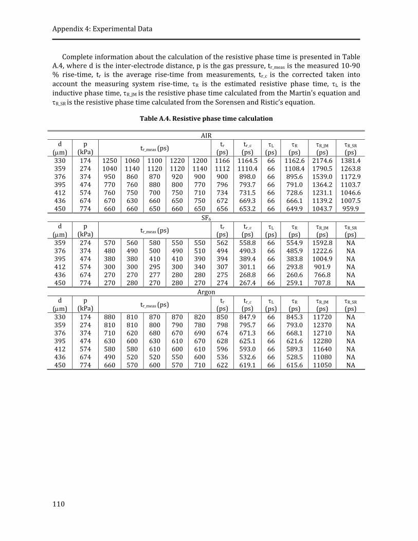
Appendix 4: Experimental Data
110
Complete information about the calculation of the resistive phase time is presented in Table A.4, where d is the inter‐electrode distance, p is the gas pressure, tr_meas is the measured 10‐90 % rise‐time, tr is the average rise‐time from measurements, tr_c is the corrected taken into account the measuring system rise‐time, R is the estimated resistive phase time, L is the inductive phase time, R_JM is the resistive phase time calculated from the Martin’s equation and R_SR is the resistive phase time calculated from the Sorensen and Ristic’s equation.
Table A.4. Resistive phase time calculation
AIR d
(m) p
(kPa) tr_meas (ps) tr (ps)
tr_c (ps)
L (ps)
R (ps)
R_JM (ps)
R_SR (ps)
330 174 1250 1060 1100 1220 1200 1166 1164.5 66 1162.6 2174.6 1381.4 359 274 1040 1140 1120 1120 1140 1112 1110.4 66 1108.4 1790.5 1263.8 376 374 950 860 870 920 900 900 898.0 66 895.6 1539.0 1172.9 395 474 770 760 880 800 770 796 793.7 66 791.0 1364.2 1103.7 412 574 760 750 700 750 710 734 731.5 66 728.6 1231.1 1046.6 436 674 670 630 660 650 750 672 669.3 66 666.1 1139.2 1007.5 450 774 660 660 650 660 650 656 653.2 66 649.9 1043.7 959.9
SF6 d
(m) p
(kPa) tr_meas (ps) tr (ps)
tr_c (ps)
L (ps)
R (ps)
R_JM (ps)
R_SR (ps)
359 274 570 560 580 550 550 562 558.8 66 554.9 1592.8 NA 376 374 480 490 500 490 510 494 490.3 66 485.9 1222.6 NA 395 474 380 380 410 410 390 394 389.4 66 383.8 1004.9 NA 412 574 300 300 295 300 340 307 301.1 66 293.8 901.9 NA 436 674 270 270 277 280 280 275 268.8 66 260.6 766.8 NA 450 774 270 280 270 280 270 274 267.4 66 259.1 707.8 NA
Argon d
(m) p
(kPa) tr_meas (ps) tr (ps)
tr_c (ps)
L (ps)
R (ps)
R_JM (ps)
R_SR (ps)
330 174 880 810 870 870 820 850 847.9 66 845.3 11720 NA 359 274 810 810 800 790 780 798 795.7 66 793.0 12370 NA 376 374 710 620 680 670 690 674 671.3 66 668.1 12710 NA 395 474 630 600 630 610 670 628 625.1 66 621.6 12280 NA 412 574 580 580 610 600 610 596 593.0 66 589.3 11640 NA 436 674 490 520 520 550 600 536 532.6 66 528.5 11080 NA 450 774 660 570 600 570 710 622 619.1 66 615.6 11050 NA

Table A.5 shows the Pulse repetition Frequency PRF from laboratory tests for air. Vg corresponds to the applied voltage, Td is the time between pulses, the PRF was calculated as the inverse of Td, and PRFA is the PRF average value.
Table A.5. Pulse Repetition Frequency Calculation
d (m)
p (kPa)
Vg (kV)
Td (ms) PRF (kHz) PRFA (kHz)
5 890 920 910 790 800 1.12 1.09 1.10 1.27 1.25 1.16
10 296 292 292 292 292 3.38 3.42 3.42 3.42 3.42 3.42
15 200 208 204 204 204 5.00 4.81 4.90 4.90 4.90 4.90
20 136 142 136 138 140 7.35 7.04 7.35 7.25 7.14 7.23
25 124 126 120 122 120 8.06 7.94 8.33 8.20 8.33 8.17
30 100 102 98 104 104 10.00 9.80 10.20 9.62 9.62 9.84
35 86 85 84 86 84 11.63 11.76 11.90 11.63 11.90 11.76
40 74 75 74 76 72 13.51 13.33 13.51 13.16 13.89 13.48
45 72 72 73 73 70 13.89 13.89 13.70 13.70 14.29 13.89
359 274
50 61 62 62 62 64 16.39 16.13 16.13 16.13 15.63 16.08
10 470 460 470 490 470 2.13 2.17 2.13 2.04 2.13 2.12
15 300 296 296 288 296 3.33 3.38 3.38 3.47 3.38 3.39
20 212 212 204 212 212 4.72 4.72 4.90 4.72 4.72 4.75
25 180 184 192 192 196 5.56 5.43 5.21 5.21 5.10 5.30
30 146 148 146 146 146 6.85 6.76 6.85 6.85 6.85 6.83
35 128 128 128 132 126 7.81 7.81 7.81 7.58 7.94 7.79
40 118 112 116 112 112 8.47 8.93 8.62 8.93 8.93 8.77
45 100 99 101 110 101 10.00 10.10 9.90 9.09 9.90 9.78
376 374
50 98 92 92 98 90 10.20 10.87 10.87 10.20 11.11 10.64
10 780 820 780 760 770 1.28 1.22 1.28 1.32 1.30 1.28
15 460 460 450 460 440 2.17 2.17 2.22 2.17 2.27 2.20
20 316 320 320 328 324 3.16 3.13 3.13 3.05 3.09 3.11
25 244 248 256 252 260 4.10 4.03 3.91 3.97 3.85 3.97
30 204 216 212 228 204 4.90 4.63 4.72 4.39 4.90 4.70
35 170 168 182 186 166 5.88 5.95 5.49 5.38 6.02 5.73
40 164 150 146 162 166 6.10 6.67 6.85 6.17 6.02 6.35
45 138 136 138 140 138 7.25 7.35 7.25 7.14 7.25 7.25
395 474
50 132 128 134 140 116 7.58 7.81 7.46 7.14 8.62 7.69
10 1180 1420 1320 1340 1360 0.85 0.70 0.76 0.75 0.74 0.76
15 650 640 620 620 650 1.54 1.56 1.61 1.61 1.54 1.57
20 490 540 520 530 510 2.04 1.85 1.92 1.89 1.96 1.93
25 340 324 332 328 312 2.94 3.09 3.01 3.05 3.21 3.06
30 324 340 260 272 288 3.09 2.94 3.85 3.68 3.47 3.37
35 272 272 276 208 268 3.68 3.68 3.62 4.81 3.73 3.86
412 574
40 280 232 260 264 208 3.57 4.31 3.85 3.79 4.81 4.02
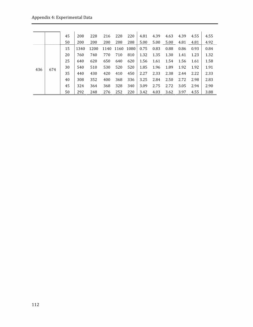
Appendix 4: Experimental Data
112
45 208 228 216 228 220 4.81 4.39 4.63 4.39 4.55 4.55
50 200 200 200 208 208 5.00 5.00 5.00 4.81 4.81 4.92
15 1340 1200 1140 1160 1080 0.75 0.83 0.88 0.86 0.93 0.84
20 760 740 770 710 810 1.32 1.35 1.30 1.41 1.23 1.32
25 640 620 650 640 620 1.56 1.61 1.54 1.56 1.61 1.58
30 540 510 530 520 520 1.85 1.96 1.89 1.92 1.92 1.91
35 440 430 420 410 450 2.27 2.33 2.38 2.44 2.22 2.33
40 308 352 400 368 336 3.25 2.84 2.50 2.72 2.98 2.83
45 324 364 368 328 340 3.09 2.75 2.72 3.05 2.94 2.90
436 674
50 292 248 276 252 220 3.42 4.03 3.62 3.97 4.55 3.88
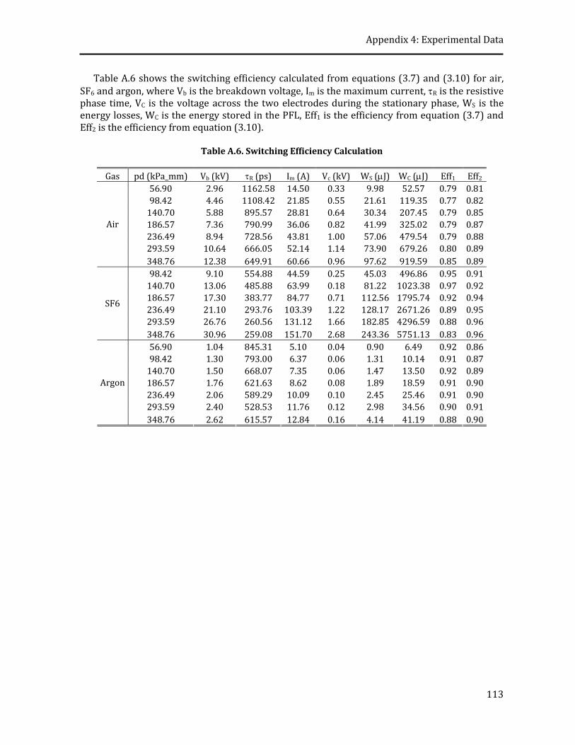
Appendix 4: Experimental Data
113
Table A.6 shows the switching efficiency calculated from equations (3.7) and (3.10) for air, SF6 and argon, where Vb is the breakdown voltage, Im is the maximum current, R is the resistive phase time, VC is the voltage across the two electrodes during the stationary phase, WS is the energy losses, WC is the energy stored in the PFL, Eff1 is the efficiency from equation (3.7) and Eff2 is the efficiency from equation (3.10).
Table A.6. Switching Efficiency Calculation
Gas pd (kPa_mm) Vb (kV) R (ps) Im (A) Vc (kV) WS (J) WC (J) Eff1 Eff256.90 2.96 1162.58 14.50 0.33 9.98 52.57 0.79 0.8198.42 4.46 1108.42 21.85 0.55 21.61 119.35 0.77 0.82140.70 5.88 895.57 28.81 0.64 30.34 207.45 0.79 0.85186.57 7.36 790.99 36.06 0.82 41.99 325.02 0.79 0.87236.49 8.94 728.56 43.81 1.00 57.06 479.54 0.79 0.88293.59 10.64 666.05 52.14 1.14 73.90 679.26 0.80 0.89
Air
348.76 12.38 649.91 60.66 0.96 97.62 919.59 0.85 0.8998.42 9.10 554.88 44.59 0.25 45.03 496.86 0.95 0.91140.70 13.06 485.88 63.99 0.18 81.22 1023.38 0.97 0.92186.57 17.30 383.77 84.77 0.71 112.56 1795.74 0.92 0.94236.49 21.10 293.76 103.39 1.22 128.17 2671.26 0.89 0.95293.59 26.76 260.56 131.12 1.66 182.85 4296.59 0.88 0.96
SF6
348.76 30.96 259.08 151.70 2.68 243.36 5751.13 0.83 0.9656.90 1.04 845.31 5.10 0.04 0.90 6.49 0.92 0.8698.42 1.30 793.00 6.37 0.06 1.31 10.14 0.91 0.87140.70 1.50 668.07 7.35 0.06 1.47 13.50 0.92 0.89186.57 1.76 621.63 8.62 0.08 1.89 18.59 0.91 0.90236.49 2.06 589.29 10.09 0.10 2.45 25.46 0.91 0.90293.59 2.40 528.53 11.76 0.12 2.98 34.56 0.90 0.91
Argon
348.76 2.62 615.57 12.84 0.16 4.14 41.19 0.88 0.90