Experiment Introduction to VHDL , Quartus II Software 7 ... · PDF fileIntroduction to VHDL ,...
20
1 | Page Experiment 7 Introduction to VHDL , Quartus II Software and FPGA Board The purpose of this laboratory is to give introduction to VHDL code using Altera Quartus II software and thus, implement it on Altera DE1 board. Stephen Brown and Zvonko Vranesic: Fundamentals of Digital Logic with VHDL Design, 3rd Edition About the Altera Quartus II Software Altera DE 1 Board Altera Quartus II Software Altera DE 1 Board VHDL (VHSIC hardware description language) is a hardware description language used in electronic design automation to describe digital and mixed- signal systems such as field-programmable gate arrays and integrated circuits. Altera Quartus II is a Computer Aided Design (CAD) software makes it easy to implement a desired logic circuit by using a pro-grammable logic device, such as a field-programmable gate array (FPGA) chip. A typical FPGA CAD flow is illustrated in Figure 1. Objective References Components
Transcript of Experiment Introduction to VHDL , Quartus II Software 7 ... · PDF fileIntroduction to VHDL ,...
1 | P a g e
Experiment
7 Introduction to VHDL , Quartus II Software and FPGA Board
The purpose of this laboratory is to give introduction to VHDL code using Altera Quartus II software and thus, implement it on Altera DE1 board.
Stephen Brown and Zvonko Vranesic: Fundamentals of Digital Logic with VHDL
Design, 3rd Edition About the Altera Quartus II Software Altera DE 1 Board
Altera Quartus II Software
Altera DE 1 Board
VHDL (VHSIC hardware description language) is a hardware description
language used in electronic design automation to describe digital and mixed-
signal systems such as field-programmable gate arrays and integrated circuits.
Altera Quartus II is a Computer Aided Design (CAD) software makes it easy
to implement a desired logic circuit by using a pro-grammable logic device, such
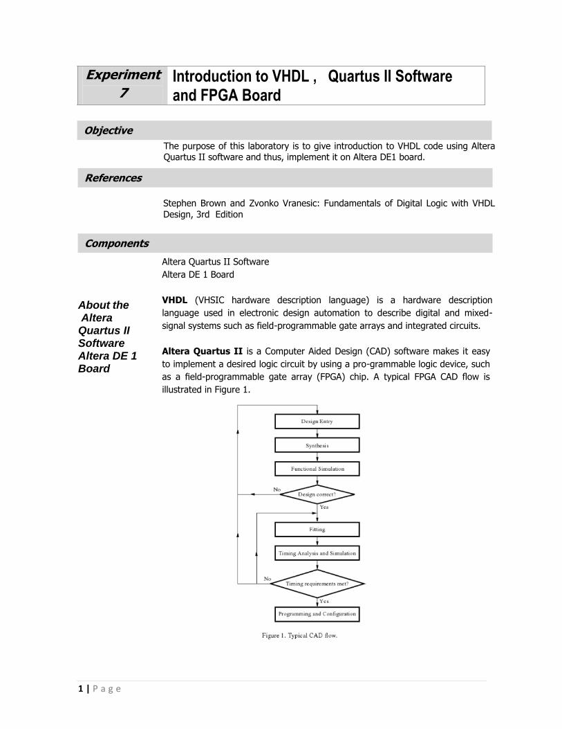
as a field-programmable gate array (FPGA) chip. A typical FPGA CAD flow is
illustrated in Figure 1.
Objective
References
Components
2 | P a g e
The CAD flow involves the following steps:
• Design Entry – the desired circuit is specified either by means of a schematic
diagram, or by using a hardware description language, such as Verilog or VHDL
• Synthesis – the entered design is synthesized into a circuit that consists of the
logic elements (LEs) provided in the FPGA chip
• Functional Simulation – the synthesized circuit is tested to verify its functional
correctness; this simulation does not take into account any timing issues
• Fitting – the CAD Fitter tool determines the placement of the LEs defined in the
netlist into the LEs in an actual FPGA chip; it also chooses routing wires in the chip
to make the required connections between specific LEs
• Timing Analysis – propagation delays along the various paths in the fitted circuit
are analyzed to provide an indication of the expected performance of the circuit
• Timing Simulation – the fitted circuit is tested to verify both its functional
correctness and timing
• Programming and Configuration – the designed circuit is implemented in a
physical FPGA chip by programming the configuration switches that configure the
LEs and establish the required wiring connections
The purpose of the Altera DE1 Development and Education board is to provide the
ideal vehicle for advanced design prototyping in the multimedia, storage, and
networking.
It uses the state-of-the-art technology in both hardware and CAD tools to expose
designers to a wide range of topics. The board offers a rich set of features that
make it suitable for use in a laboratory environment for university and college
courses, for a variety of design projects, as well as for the development of
sophisticated digital systems.
3 | P a g e
Part A: Create a New Project
1. On starting Altera Quartus II, you should be faced with a screen like this:
Figure 1: The main Quartus II display
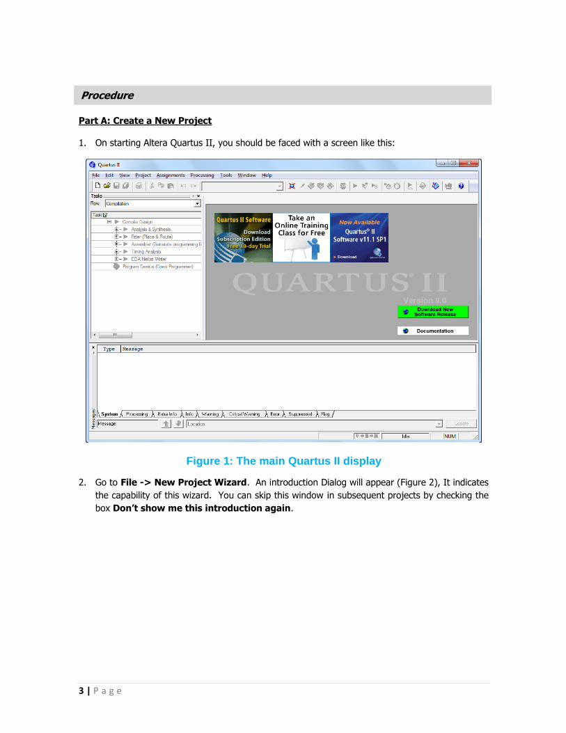
2. Go to File -> New Project Wizard. An introduction Dialog will appear (Figure 2), It indicates
the capability of this wizard. You can skip this window in subsequent projects by checking the
box Don’t show me this introduction again.
Procedure
4 | P a g e
Figure 2: Tasks performed by the wizard
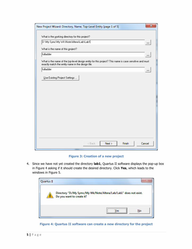
3. Press Next to get the window shown in Figure 3. Choose the location of your working directory
and type in the name of your project (let’s use fulladder) as shown in Figure 3. Press Next.
5 | P a g e
Figure 3: Creation of a new project
4. Since we have not yet created the directory lab1, Quartus II software displays the pop-up box
in Figure 4 asking if it should create the desired directory. Click Yes, which leads to the
windows in Figure 5.
Figure 4: Quartus II software can create a new directory for the project
6 | P a g e
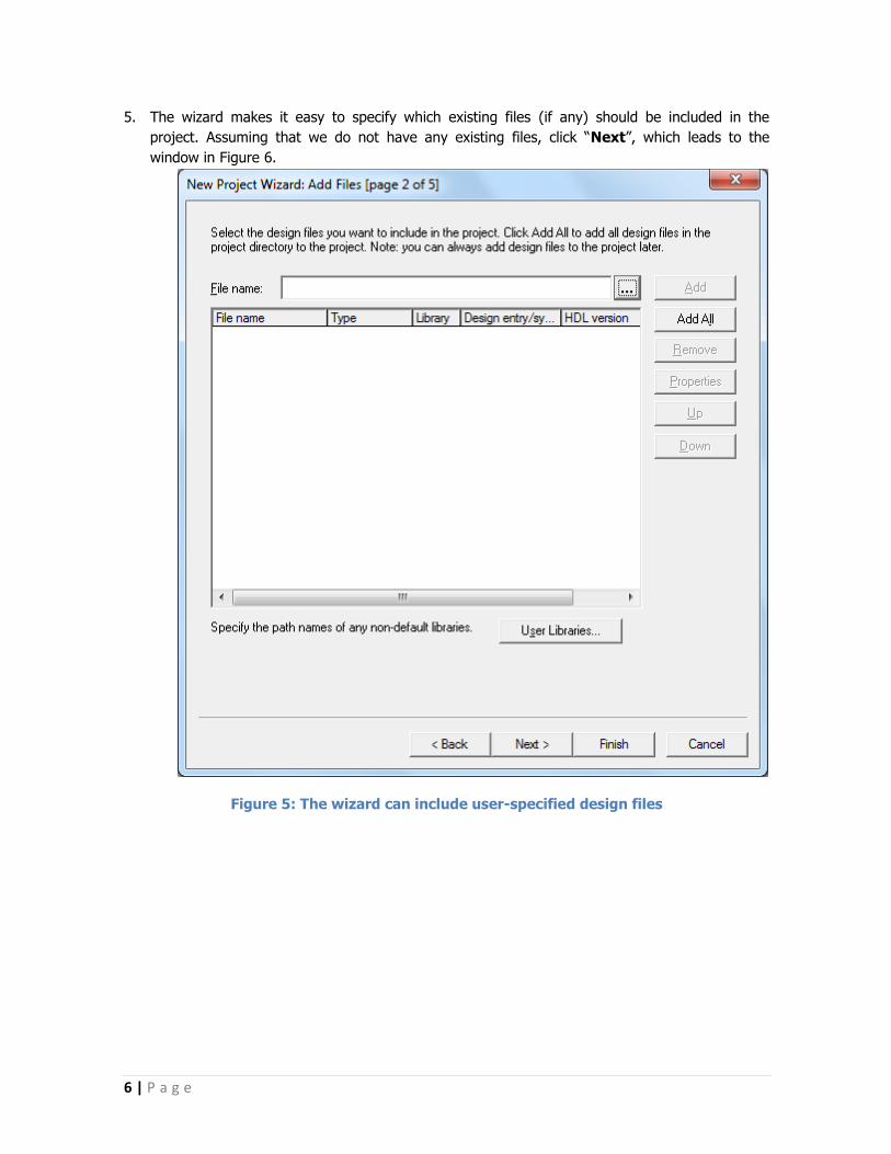
5. The wizard makes it easy to specify which existing files (if any) should be included in the
project. Assuming that we do not have any existing files, click “Next”, which leads to the
window in Figure 6.
Figure 5: The wizard can include user-specified design files
7 | P a g e
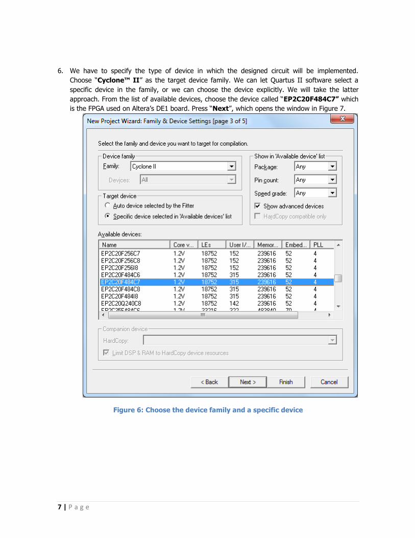
6. We have to specify the type of device in which the designed circuit will be implemented.
Choose “Cyclone™ II” as the target device family. We can let Quartus II software select a
specific device in the family, or we can choose the device explicitly. We will take the latter
approach. From the list of available devices, choose the device called “EP2C20F484C7” which
is the FPGA used on Altera’s DE1 board. Press “Next”, which opens the window in Figure 7.
Figure 6: Choose the device family and a specific device
8 | P a g e
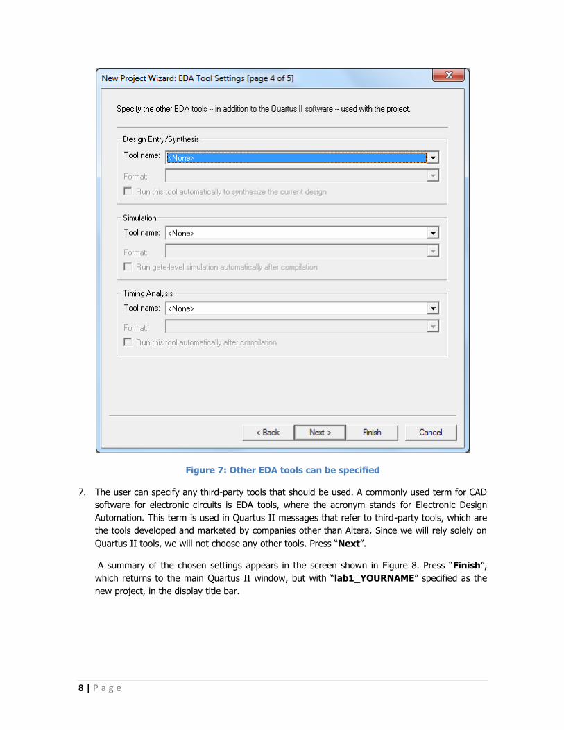
Figure 7: Other EDA tools can be specified
7. The user can specify any third-party tools that should be used. A commonly used term for CAD
software for electronic circuits is EDA tools, where the acronym stands for Electronic Design
Automation. This term is used in Quartus II messages that refer to third-party tools, which are
the tools developed and marketed by companies other than Altera. Since we will rely solely on
Quartus II tools, we will not choose any other tools. Press “Next”.
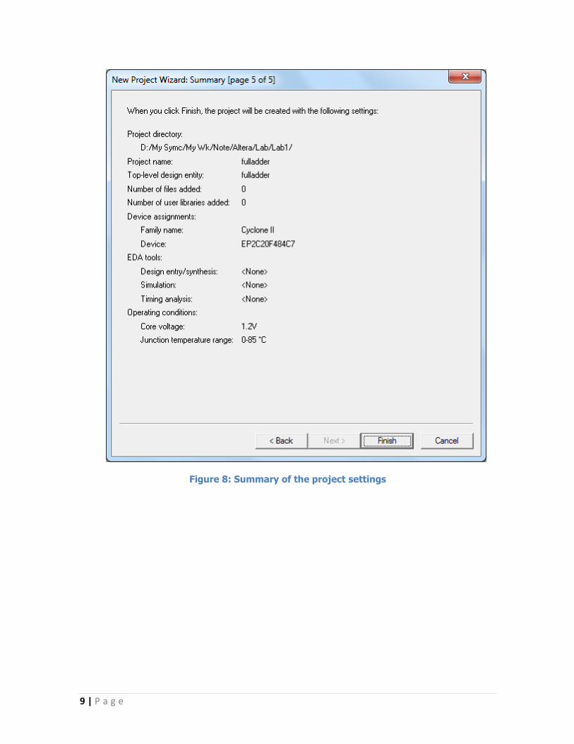
A summary of the chosen settings appears in the screen shown in Figure 8. Press “Finish”,
which returns to the main Quartus II window, but with “lab1_YOURNAME” specified as the
new project, in the display title bar.
9 | P a g e
Figure 8: Summary of the project settings
10 | P a g e
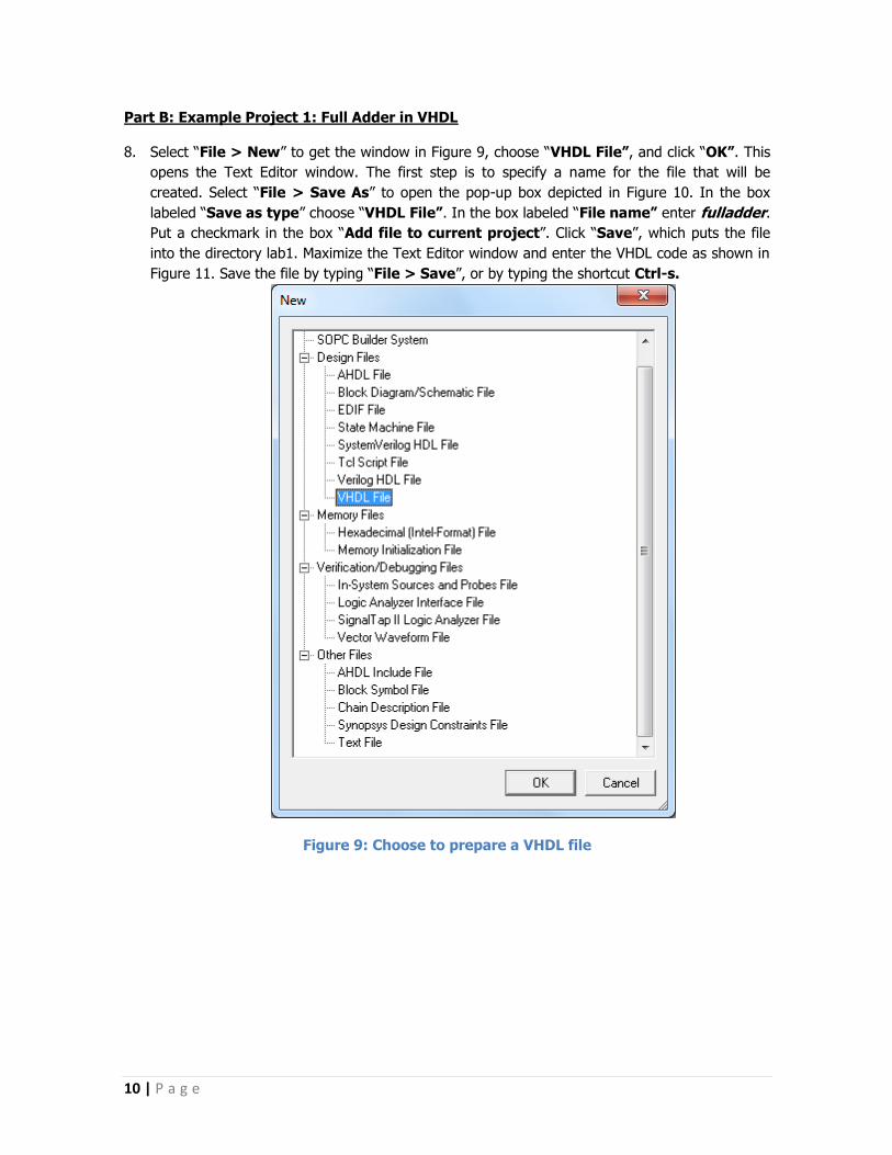
Part B: Example Project 1: Full Adder in VHDL
8. Select “File > New” to get the window in Figure 9, choose “VHDL File”, and click “OK”. This
opens the Text Editor window. The first step is to specify a name for the file that will be
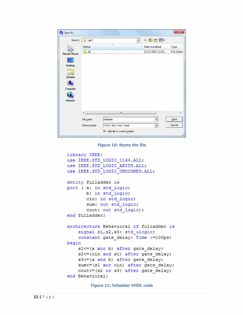
created. Select “File > Save As” to open the pop-up box depicted in Figure 10. In the box
labeled “Save as type” choose “VHDL File”. In the box labeled “File name” enter fulladder.
Put a checkmark in the box “Add file to current project”. Click “Save”, which puts the file
into the directory lab1. Maximize the Text Editor window and enter the VHDL code as shown in
Figure 11. Save the file by typing “File > Save”, or by typing the shortcut Ctrl-s.
Figure 9: Choose to prepare a VHDL file
11 | P a g e
Figure 10: Name the file
Figure 11: fulladder VHDL code

12 | P a g e
Part C: Code Compilation
The code in the file fulladder is processed by several Quartus II tools that analyze the code,
synthesize the circuit, and generate an implementation of it for the target chip. These tools are
controlled by the application program called the Compiler.
1. Run the Compiler by selecting “Processing > Start Compilation”, or by clicking on the
toolbar icon that looks like a purple triangle. As the compilation moves through various
stages, its progress is reported in a window on the left side of the Quartus II display.
Successful (or unsuccessful) compilation is indicated in a pop-up box. Acknowledge it by
clicking “OK”, which leads to the Quartus II display in Figure 12. In the message window,
at the bottom of the figure, various messages are displayed. In case of errors, there will be
appropriate messages given. When the compilation is finished, a compilation report is
produced. A window showing this report is opened automatically, as seen in Figure 12. The
window can be resized, maximized, or closed in the normal way, and it can be opened at
any time either by selecting “Processing > Compilation Report” or by clicking on the
icon .
Figure 12: Display after a successful compilation
13 | P a g e
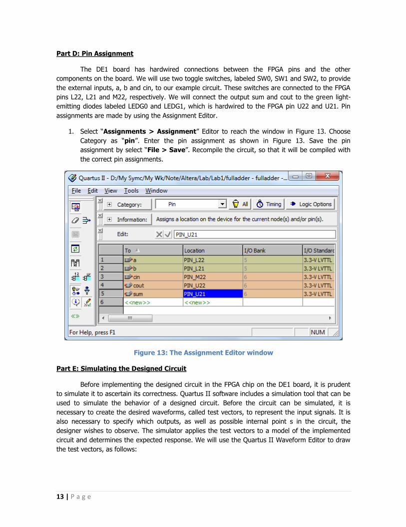
Part D: Pin Assignment
The DE1 board has hardwired connections between the FPGA pins and the other
components on the board. We will use two toggle switches, labeled SW0, SW1 and SW2, to provide
the external inputs, a, b and cin, to our example circuit. These switches are connected to the FPGA
pins L22, L21 and M22, respectively. We will connect the output sum and cout to the green light-
emitting diodes labeled LEDG0 and LEDG1, which is hardwired to the FPGA pin U22 and U21. Pin
assignments are made by using the Assignment Editor.
1. Select “Assignments > Assignment” Editor to reach the window in Figure 13. Choose
Category as “pin”. Enter the pin assignment as shown in Figure 13. Save the pin
assignment by select “File > Save”. Recompile the circuit, so that it will be compiled with
the correct pin assignments.
Figure 13: The Assignment Editor window
Part E: Simulating the Designed Circuit
Before implementing the designed circuit in the FPGA chip on the DE1 board, it is prudent
to simulate it to ascertain its correctness. Quartus II software includes a simulation tool that can be
used to simulate the behavior of a designed circuit. Before the circuit can be simulated, it is
necessary to create the desired waveforms, called test vectors, to represent the input signals. It is
also necessary to specify which outputs, as well as possible internal point s in the circuit, the
designer wishes to observe. The simulator applies the test vectors to a model of the implemented
circuit and determines the expected response. We will use the Quartus II Waveform Editor to draw
the test vectors, as follows:
14 | P a g e
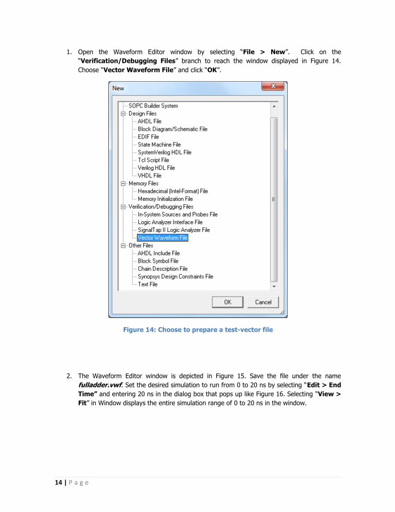
1. Open the Waveform Editor window by selecting “File > New”. Click on the
“Verification/Debugging Files” branch to reach the window displayed in Figure 14.
Choose “Vector Waveform File” and click “OK”.
Figure 14: Choose to prepare a test-vector file
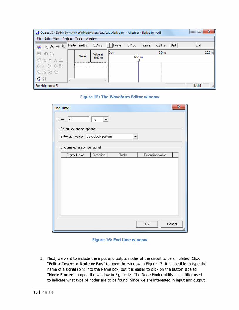
2. The Waveform Editor window is depicted in Figure 15. Save the file under the name
fulladder.vwf. Set the desired simulation to run from 0 to 20 ns by selecting “Edit > End
Time” and entering 20 ns in the dialog box that pops up like Figure 16. Selecting “View >
Fit” in Window displays the entire simulation range of 0 to 20 ns in the window.
15 | P a g e
Figure 15: The Waveform Editor window
Figure 16: End time window
3. Next, we want to include the input and output nodes of the circuit to be simulated. Click
“Edit > Insert > Node or Bus” to open the window in Figure 17. It is possible to type the
name of a signal (pin) into the Name box, but it is easier to click on the button labeled
“Node Finder” to open the window in Figure 18. The Node Finder utility has a filter used
to indicate what type of nodes are to be found. Since we are interested in input and output
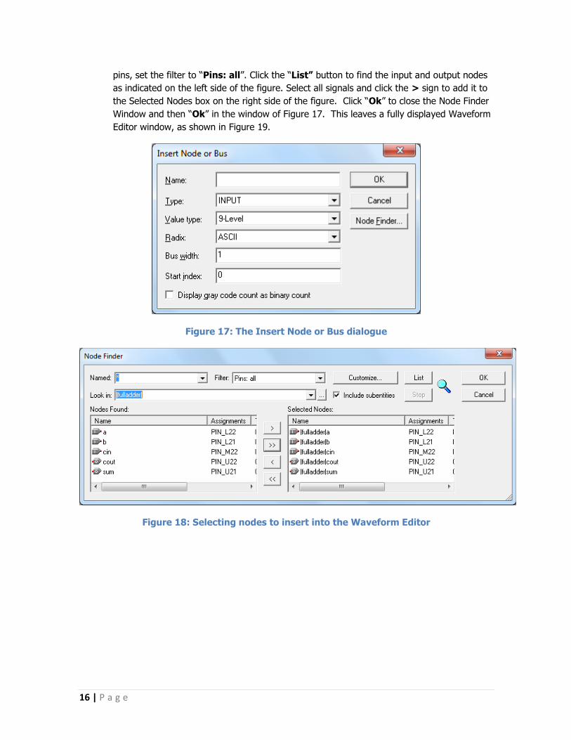
16 | P a g e
pins, set the filter to “Pins: all”. Click the “List” button to find the input and output nodes
as indicated on the left side of the figure. Select all signals and click the > sign to add it to
the Selected Nodes box on the right side of the figure. Click “Ok” to close the Node Finder
Window and then “Ok” in the window of Figure 17. This leaves a fully displayed Waveform
Editor window, as shown in Figure 19.
Figure 17: The Insert Node or Bus dialogue
Figure 18: Selecting nodes to insert into the Waveform Editor
17 | P a g e
Figure 19: The nodes needed for simulation
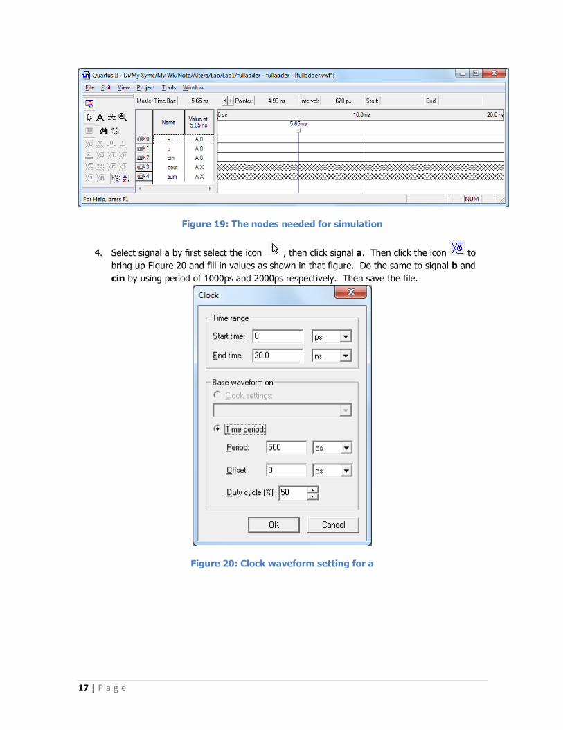
4. Select signal a by first select the icon , then click signal a. Then click the icon to
bring up Figure 20 and fill in values as shown in that figure. Do the same to signal b and
cin by using period of 1000ps and 2000ps respectively. Then save the file.
Figure 20: Clock waveform setting for a
18 | P a g e
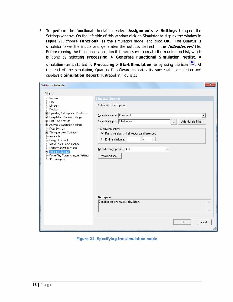
5. To perform the functional simulation, select Assignments > Settings to open the
Settings window. On the left side of this window click on Simulator to display the window in
Figure 21, choose Functional as the simulation mode, and click OK. The Quartus II
simulator takes the inputs and generates the outputs defined in the fulladder.vwf file.
Before running the functional simulation it is necessary to create the required netlist, which
is done by selecting Processing > Generate Functional Simulation Netlist. A
simulation run is started by Processing > Start Simulation, or by using the icon . At
the end of the simulation, Quartus II software indicates its successful completion and
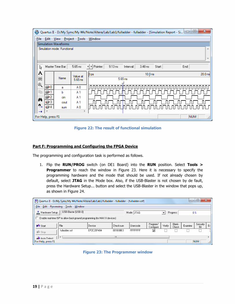
displays a Simulation Report illustrated in Figure 22.
Figure 21: Specifying the simulation mode
19 | P a g e
Figure 22: The result of functional simulation
Part F: Programming and Configuring the FPGA Device
The programming and configuration task is performed as follows.
1. Flip the RUN/PROG switch (on DE1 Board) into the RUN position. Select Tools >
Programmer to reach the window in Figure 23. Here it is necessary to specify the
programming hardware and the mode that should be used. If not already chosen by
default, select JTAG in the Mode box. Also, if the USB-Blaster is not chosen by de fault,
press the Hardware Setup... button and select the USB-Blaster in the window that pops up,
as shown in Figure 24.
Figure 23: The Programmer window

20 | P a g e
Figure 24: The updated Programmer window
2. Observe that the configuration file fulladder.sof is listed in the window in Figure 24. If the
file is not already listed, then click Add File and select it. This is a binary file produced by
the Compiler’s Assembler module, which contains the data needed to configure the FPGA
device. The extension .sof stands for SRAM Object File. Note also that the device selected is
EP2C20F484, which is the FPGA device used on the DE1 board. Click on the
Program/Configure check box, as shown in Figure 23. Now, press Start in the window in
Figure 23. An LED on the board will light up when the configuration data has been
downloaded successfully. If you see an error reported by Quartus II software indicating
that programming failed, then check to ensure that the board is properly powered on.