Experiment # (3) AM Modulator - الصفحات الشخصية | الجامعة...
14
1 Islamic University of Gaza Faculty of Engineering Electrical Department Communications Engineering I (Lab.) Prepared by: Eng. Omar A. Qarmout Eng. Mohammed K. Abu Foul Experiment # (3) AM Modulator Experiment theory: In amplitude modulation (AM), we utilize the amplitude of the audio signal to modulate the amplitude of carrier signal, which means that the amplitude of carrier signal will be varied with the amplitude of the audio signal. The wave form of AM modulation is shown in figure 3- 1 and its block diagram is shown in figure 3-2. In figure 3-2, we know that in order to generate the AM signal, we just need to add a DC signal with the audio signal, and then multiply the added signal with the carrier signal. Figure 3-1 Signal waveform of amplitude modulation Figure 3-2 Block diagram of AM modulation
Transcript of Experiment # (3) AM Modulator - الصفحات الشخصية | الجامعة...

1
Islamic University of Gaza
Faculty of Engineering
Electrical Department
Communications Engineering I (Lab.)
Prepared by:
Eng. Omar A. Qarmout
Eng. Mohammed K. Abu Foul
Experiment # (3)
AM Modulator
Experiment theory:
In amplitude modulation (AM), we utilize the amplitude of the audio signal to modulate
the amplitude of carrier signal, which means that the amplitude of carrier signal will be varied
with the amplitude of the audio signal. The wave form of AM modulation is shown in figure 3-
1 and its block diagram is shown in figure 3-2. In figure 3-2, we know that in order to generate
the AM signal, we just need to add a DC signal with the audio signal, and then multiply the
added signal with the carrier signal.
Figure 3-1 Signal waveform of amplitude modulation
Figure 3-2 Block diagram of AM modulation

2
Let the audio signal be and carrier signal be , then the
amplitude modulation can be expressed as:
Where
=
: DC signal amplitude.
: Audio signal amplitude.
: Carrier signal amplitude.
: Audio signal frequency.
: Carrier signal frequency.
M : Modulation index or depth of modulation.
From equation (3-1), we notice that the variation of the magnitude
of the carrier signal can be controlled by parameter 'm'. This
means that we can change the magnitude of the audio signal ( ) or DC signal ( ) to control
the level or depth of the carrier signal. Therefore, this parameter 'm' is known as the modulation
index.
Besides, we can also rewrite equation 3-1 as:
The first term represents double side band signals; the second term represent carrier
signal. From equation 3-2, we can sketch the frequency spectrum of amplitude modulation as
shown in figure 3-3. Since the audio signal is hidden in the double sidebands and the carrier
signal does not contain any massage, there for the power is consumed in carrier during
transmission of amplitude modulation signal. For this reason, the transmission efficiency of
AM modulation is lower than double sidebands suppressed carrier (DSB-SC) modulation but
its demodulation is circuit is much simpler.
Figure 3-3 Frequency Spectrum of amplitude modulation signal

3
There is an important parameter 'm' in equation 3-1 called modulation index or depth of
modulation. Normally it is represented in percentage, so we also call modulation percentage.
Modulation index is an important parameter in equation 3-1. The definition is as follow:
Generally, the magnitude of DC signal is not easy to measure; therefore we express the
modulation index in another form:
Where and as shown in figure 3-1 are and .
We know that at amplitude modulation, the audio signal is hidden in the double
sidebands, so if the double sideband signals are getting stronger, the transmission efficiency is
getting better. From equation 3-2, we know that the double sideband signals are proportional to
the modulation index. Thus the larger the modulation index, the better the transmission
efficiency.
Normally modulation index is smaller equal to 1. If greater than 1, we call it over
modulation as shown in figure 3-4. Figure 3-4 shows the wave form of the over modulation. In
figure 3-4, we can see that the variation of carrier signal is no longer a sinusoidal wave. It is
rather a distorted sinusoidal wave, therefore, this kind of AM signal is unable to demodulate
and recover to the original by using the envelop detection in next experiment.
Figure 3-4 waveform of the over modulation.
As we know that the AM modulator can be implemented by using a multiplier. However, in
electronics circuit, the multiplier is constructed by the non linear characteristics of active
component. Therefore, in this experiment, we will discuss the design of AM modulator by
using a signal transistor and balanced modulator.

4
1- Transistor AM Modulator
The circuit diagram of transistor AM modulator is shown in figure 3-5. In figure 3-5, the
audio signal ( ) will pass through a transformer and send into the base of the
transistor. The carrier signal ( ) also passes through a transformer and send into
the emitter of the transistor. These two signals will form a small amount of small signal voltage
difference at the base and the emitter of the transistor. The small signal voltage difference is:
Then at the collector of the transistor, this voltage difference will produce a small signal
collector current as:
Expand equation 3-6 by Taylor's expansion, and then we get:
Figure 3-5 Circuit diagram of transistor AM modulation
In equation 3-7, we notice that after the audio signal and the carrier signal input into the
base and emitter of the transistor, we can obtain , and
signals at the collector. In figure 3-5, the inductor , capacitor
and resistor comprise a high-pass filter, which used to obtain the modulated AM signal.
Capacitor is the coupling capacitor. Capacitors and are the bypass capacitors.
Resistors and are bias resistors. Variable resistor is used to change the operation
point of the transistor and it also used to control the magnitude of the carrier, which input into
the collector of the transistor. Therefore, it can adjust the output signal waveform of the
modulator.

5
2- MC1496 AM Modulator
The main different between the design of AM modulator by using balanced modulator
and the transistor is that we can used the theory of balanced modulator to cancel out the
unwanted harmonics signal, which is produced by the non linear characteristic of the transistor,
so the remain signal is AM signal. In this part we utilize the balance modulator (MC1496) to
implement AM modulator.
Follow the variation of input signal frequency, the balance modulator (MC1496) can become a
frequency multiplier, AM Modulator or double sidebands suppressed carrier modulator (DSB-
SC Modulator). Its input signal, output signal and circuit characteristics as shown in table 3-1.
Table 3-1: Three different types of modulation signal produced by different signals frequency of balanced modulator.
Figure 3-6: Internal circuit diagram of MC1496
Figure 3-6 is the internal circuit diagram of MC1496, where and
comprise an electric current source, which can supply DC bias current for and .
and comprise a differential combination to drive the dual differential amplifier
constructed by and . Pin 1 and 4 are the inputs of the audio signal, after that this
signal will be amplified by the differential amplifier, which is comprise by and . Pin 8
and 10 are the inputs carrier signal. Then the amplified audio signal will be multiplied by the
carrier signal at the dual differential amplifier constructed by and , respectively.

6
The resistor between pins 2 and 3 controls the gain of the balanced modulator; the
resistor of pin 5 determines the magnitude of bias current for amplifier.
Figure 3-7 is the circuit diagram of the AM modulator. We can see that the carrier
signal and audio signal belong to single ended input. The carrier signal input is from pin 10 and
the audio signal input is from pin 1. Therefore determine the gain of the whole circuit and
determine the magnitude of bias current. If we adjust the variable resistor or change the
input amplitude of the audio signal, then we can control the percentage modulation of the AM
modulator.
Figure 3-7: Circuit diagram of amplitude modulation by utilizing MC1496.

7
Experiment items:
Experiment 1: Transistor AM modulator
1. Refer to the circuit diagram in figure 3.5 or figure ACS3-1 on ETEK ACS-3000-02
module.
2. At audio signal input port (Audio I/P), input 100 mV amplitude, 1 kHz sine wave
frequency; at carrier signal input port (Carrier I/P), input 300 mV amplitude, 500 kHz
sine wave frequency.
3. By using Oscilloscope, observe on output signal waveforms of AM output port (AM
O/P). Adjust VR1 so that the modulated AM signal is maximum without distortion.
Then records the measured results in table 3.2.
4. By using Oscilloscope, observe on output signal waveforms of the base (TP1) and
collector (TP3) of the transistor. Then records the measured results in table 3.2.
5. By using Oscilloscope, observe on output signal waveforms of the mixing (TP2) of the
transistor. Then records the measured results in table 3.2.
6. Substitute the measured results into equation 3.4, find the modulation percentage and
record in table 3.2. 7. According to the input signals in table 3.2, repeat step 4 to 6 and record the measured
results in table 3.2.
8. According to the input signals in table 3.3, repeat step 2 to 6 and record the measured
results in table 3.3.
Experiment 2: MC1496 AM modulator
Experiment 2.1: Observe on the variation of AM modulator by changing the
amplitude and frequency of audio signal.
1. Refer to the circuit diagram in figure 3.7 or figure ACS3-2 on ETEK ACS-3000-02
module. Let J1 be short circuit, J2 be open circuit; i.e. R10=6.8 kΩ
2. At audio signal input port (Audio I/P), input 600 mV amplitude, 1 kHz sine wave
frequency; at carrier signal input port (Carrier I/P), input 300 mV amplitude, 500 kHz
sine wave frequency.
3. By using Oscilloscope, observe on output signal waveforms of AM output ports (AM
O/P1 and AM O/P2). Adjust VR2 so that the signal at AM O/P1 is maximum without
distortion. Adjust VR1 so that the modulation index of the AM signal reaches 50%.
Then records the measured results in table 3.4.
4. By using Oscilloscope, observe on output signal waveforms of the pin 1 (TP3), pin 4
(TP4), pin 8 (TP1), and pin 10 (TP2) of the balanced modulator. Then record the
measured results in table 3.4.
5. By using Oscilloscope, observe on output signal waveforms of the mixing (TP5 and
TP6) of the balanced modulator and the bias operation point (TP7). Then record the
measured results in table 3.4.
6. Substitute the measured results into equation 3.4, find the modulation percentage and
record in table 3.4.
7. According to the input signals in table 3.4, repeat step 4 to 6 and record the measured
results in table 3.4.

8
8. Let J1 be open circuit, and J2 be short circuit; i.e. change the resistor R10=6.8 kΩ to
R12=3.3 kΩ. Repeat step 2 to step 7 and record the measured results in table 3.5.
9. According to the input signals in table 3.6, repeat step 4 to 6 and record the measured
results in table 3.6.
Experiment 2.2: Observe on the variation of AM modulator by changing the
amplitude and frequency of carrier signal.
1. Refer to the circuit diagram in figure 3.7 or figure ACS3-2 on ETEK ACS-3000-02
module. Let J1 be open circuit, J2 be open circuit; i.e. R12=3.3 kΩ
2. At audio signal input port (Audio I/P), input 600 mV amplitude, 1 kHz sine wave
frequency; at carrier signal input port (Carrier I/P), input 200 mV amplitude, 500 kHz
sine wave frequency.
3. By using Oscilloscope, observe on output signal waveforms of AM output ports (AM
O/P1 and AM O/P2). Adjust VR2 so that the signal at AM O/P1 is maximum without
distortion. Adjust VR1 so that the modulation index of the AM signal reaches 50%.
Then records the measured results in table 3.7.
4. By using Oscilloscope, observe on output signal waveforms of the pin 1 (TP3), pin 4
(TP4), pin 8 (TP1), and pin 10 (TP2) of the balanced modulator. Then record the
measured results in table 3.7.
5. By using Oscilloscope, observe on output signal waveforms of the mixing (TP5 and
TP6) of the balanced modulator and the bias operation point (TP7). Then record the
measured results in table 3.7.
6. Substitute the measured results into equation 3.4, find the modulation percentage and
record in table 3.7.
7. According to the input signals in table 3.7, repeat step 4 to 6 and record the measured
results in table 3.7.
8. According to the input signals in table 3.8, repeat step 2 to 6 and record the measured
results in table 3.8.
Experiment 2.3: Observe on the variation of AM modulator by changing the
Variable resistor VR1
1. Refer to the circuit diagram in figure 3.7 or figure ACS3-2 on ETEK ACS-3000-02
module. Let J1 be open circuit, J2 be open circuit; i.e. R12=3.3 kΩ
2. At audio signal input port (Audio I/P), input 600 mV amplitude, 1 kHz sine wave
frequency; at carrier signal input port (Carrier I/P), input 300 mV amplitude, 500 kHz
sine wave frequency.
3. By using Oscilloscope, observe on output signal waveforms of AM output ports (AM
O/P1 and AM O/P2). Adjust VR1 so that the modulation index of the AM signal
reaches 30%. Then records the measured results in table 3.9.
4. Substitute the measured results into equation 3.4, find the modulation percentage and
record in table 3.9.
5. According to the input signals in table 3.9, repeat step 2 to 4 and record the measured
results in table 3.9.

9
Experiment 2.4: Observe on the variation of AM modulator by changing the
Variable resistor VR2
1. Refer to the circuit diagram in figure 3.7 or figure ACS3-2 on ETEK ACS-3000-02
module. Let J1 be open circuit, J2 be open circuit; i.e. R12=3.3 kΩ
2. At audio signal input port (Audio I/P), input 600 mV amplitude, 1 kHz sine wave
frequency; at carrier signal input port (Carrier I/P), input 300 mV amplitude, 500 kHz
sine wave frequency.
3. By using Oscilloscope, observe on output signal waveforms of AM output ports (AM
O/P1 and AM O/P2). Adjust VR1 so that the modulation index of the AM signal
reaches 50%.
4. Adjust VR2 so that the resistance is 0 Ω, 5 kΩ and 10 kΩ, the others remain. Then
record the measured results in table 3.10.

11
Measured results: Transistor AM modulator.
Table 3-2: Observe on the variation of AM modulator by changing the amplitude of audio signal.
(fm=1 kHz, fc=500 kHz, Vc=300 mV)
Output signals ports Audio signal amplitudes
100 mV 150 mV
AM O/P
TP1
TP3
TP2
Modulation Index
Emax=……….
Emin=……….
m=………….%
Emax=……….
Emin=……….
m=………….%
Table 3-3: Observe on the variation of AM modulator by changing the frequency of audio signal.
(Vm=100 mV, fc=500 kHz, Vc=300 mV)
Output signals ports Audio signal frequencies
100 Hz 400 Hz
AM O/P
TP1
TP3
TP2
Modulation Index
Emax=……….
Emin=……….
m=………….%
Emax=……….
Emin=……….
m=………….%

11
MC 1496 AM modulator
Table 3-4: Observe on the variation of AM modulator by changing the amplitude of audio signal.
(fm=1 kHz, fc=500 kHz, Vc=300 mV, R10=6.8 kΩ)
Output signals ports Audio signal Amplitudes
600 mV 300 mV
AM O/P1
AM O/P2
TP1
TP2
TP3
TP4
TP5
TP6
TP7
Modulation Index
Emax=……….
Emin=……….
m=………….%
Emax=……….
Emin=……….
m=………….%
NOTE:
Table 3-5: Repeat table 3.4 when R12=3.3 kΩ

12
Table 3-6: Observe on the variation of AM modulator by changing the frequency of audio signal.
(Vm=600 mV, fc=500 kHz, Vc=300 mV, R12=3.3 kΩ)
Output signals ports Audio signal frequencies
1 kHz 2 kHz
AM O/P1
AM O/P2
TP1
TP2
TP3
TP4
TP5
TP6
TP7
Modulation Index
Emax=……….
Emin=……….
m=………….%
Emax=……….
Emin=……….
m=………….%
Table 3-7: Observe on the variation of AM modulator by changing the amplitude of carrier signal.
(Vm=600 mV, fm=1 kHz, fc=500 kHz, R12=3.3 kΩ)
Output signals ports Carrier signal amplitudes
200 mV 300 mV
AM O/P1
AM O/P2
TP1
TP2
TP3
TP4

13
TP5
TP6
TP7
Modulation Index
Emax=……….
Emin=……….
m=………….%
Emax=……….
Emin=……….
m=………….%
Table 3-8: Observe on the variation of AM modulator by changing the frequency of carrier signal.
(Vm=600 mV, fm=1 kHz, Vc=300 mV, R12=3.3 kΩ)
Output signals ports Carrier signal frequencies
500 kHz 1 MHz
AM O/P1
AM O/P2
TP1
TP2
TP3
TP4
TP5
TP6
TP7
Modulation Index
Emax=……….
Emin=……….
m=………….%
Emax=……….
Emin=……….
m=………….%
14
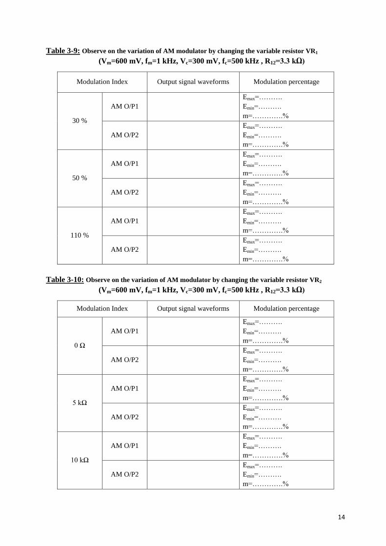
Table 3-9: Observe on the variation of AM modulator by changing the variable resistor VR1
(Vm=600 mV, fm=1 kHz, Vc=300 mV, fc=500 kHz , R12=3.3 kΩ)
Modulation Index Output signal waveforms Modulation percentage
30 %
AM O/P1
Emax=……….
Emin=……….
m=………….%
AM O/P2
Emax=……….
Emin=……….
m=………….%
50 %
AM O/P1
Emax=……….
Emin=……….
m=………….%
AM O/P2
Emax=……….
Emin=……….
m=………….%
110 %
AM O/P1
Emax=……….
Emin=……….
m=………….%
AM O/P2
Emax=……….
Emin=……….
m=………….%
Table 3-10: Observe on the variation of AM modulator by changing the variable resistor VR2
(Vm=600 mV, fm=1 kHz, Vc=300 mV, fc=500 kHz , R12=3.3 kΩ)
Modulation Index Output signal waveforms Modulation percentage
0 Ω
AM O/P1
Emax=……….
Emin=……….
m=………….%
AM O/P2
Emax=……….
Emin=……….
m=………….%
5 kΩ
AM O/P1
Emax=……….
Emin=……….
m=………….%
AM O/P2
Emax=……….
Emin=……….
m=………….%
10 kΩ
AM O/P1
Emax=……….
Emin=……….
m=………….%
AM O/P2
Emax=……….
Emin=……….
m=………….%