Exciton Dynamics in InSb Colloidal Quantum Dots - … · Exciton Dynamics in InSb Colloidal Quantum...
18
Exciton Dynamics in InSb Colloidal Quantum Dots SILLS, Andrew, HARRISON, Paul and CALIFANO, Marco Available from Sheffield Hallam University Research Archive (SHURA) at: http://shura.shu.ac.uk/11830/ This document is the author deposited version. You are advised to consult the publisher's version if you wish to cite from it. Published version SILLS, Andrew, HARRISON, Paul and CALIFANO, Marco (2016). Exciton Dynamics in InSb Colloidal Quantum Dots. The Journal of Physical Chemistry Letters, 7 (1), 31-35. Repository use policy Copyright © and Moral Rights for the papers on this site are retained by the individual authors and/or other copyright owners. Users may download and/or print one copy of any article(s) in SHURA to facilitate their private study or for non- commercial research. You may not engage in further distribution of the material or use it for any profit-making activities or any commercial gain. Sheffield Hallam University Research Archive http://shura.shu.ac.uk
Transcript of Exciton Dynamics in InSb Colloidal Quantum Dots - … · Exciton Dynamics in InSb Colloidal Quantum...
Exciton Dynamics in InSb Colloidal Quantum Dots
SILLS, Andrew, HARRISON, Paul and CALIFANO, Marco
Available from Sheffield Hallam University Research Archive (SHURA) at:
http://shura.shu.ac.uk/11830/
This document is the author deposited version. You are advised to consult the publisher's version if you wish to cite from it.
Published version
SILLS, Andrew, HARRISON, Paul and CALIFANO, Marco (2016). Exciton Dynamics in InSb Colloidal Quantum Dots. The Journal of Physical Chemistry Letters, 7 (1), 31-35.
Repository use policy
Copyright © and Moral Rights for the papers on this site are retained by the individual authors and/or other copyright owners. Users may download and/or print one copy of any article(s) in SHURA to facilitate their private study or for non-commercial research. You may not engage in further distribution of the material or use it for any profit-making activities or any commercial gain.
Sheffield Hallam University Research Archivehttp://shura.shu.ac.uk

Exciton Dynamics in InSb Colloidal Quantum Dots
Andrew Sills,† Paul Harrison,‡ and Marco Califano∗,†
Institute of Microwaves and Photonics, School of Electronic and Electrical Engineering,
University of Leeds, Leeds LS2 9JT, United Kingdom , and Materials and Engineering Research
Institute Sheffield Hallam University, Sheffield S1 1WB, United Kingdom
E-mail: [email protected]
∗To whom correspondence should be addressed†Institute of Microwaves and Photonics, School of Electronic and Electrical Engineering, University of
Leeds, Leeds LS2 9JT, United Kingdom‡Materials and Engineering Research Institute Sheffield Hallam University, Sheffield S1 1WB, United
Kingdom
1
Abstract
Extraordinarily fast biexciton decay times and unexpectedly large optical gaps are
two striking features observed in InSb colloidal quantum dots that have remained
so far unexplained. The former, should its origin be identified as an Auger recom-
bination process, would have important implications regarding carrier multiplication
efficiency, suggesting these nanostructures as potentially ideal activematerials in pho-
tovoltaic devices. The latter could offer new insights into the factors that influence
the electronic structure, and consequently the optical properties, of systems with re-
duced dimensionality, and provide additional means to fine tune them. Using the
state-of-the-art atomistic semiempirical pseudopotential method we unveil the sur-
prising origins of these features and show that a comprehensive explanation for these
properties requires delving deep into the atomistic detail of these nanostructures and
is, therefore, outside the reach of less sophisticated, albeit more popular, theoretical
approaches.
2
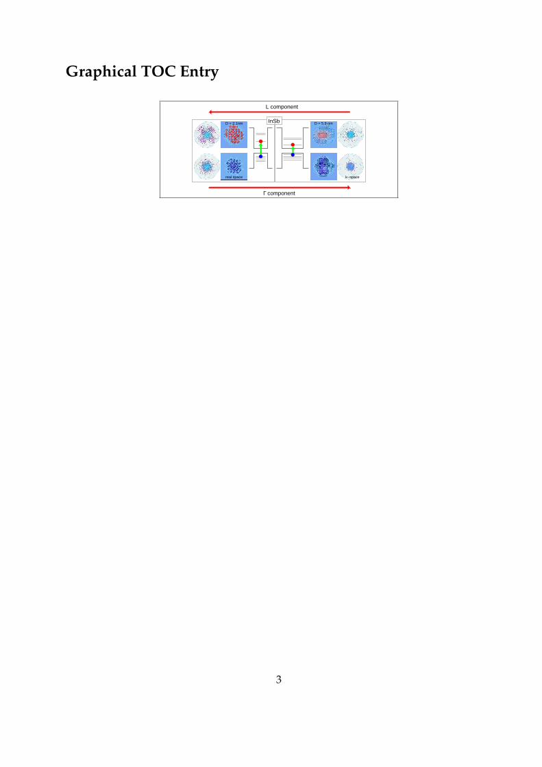
Graphical TOC Entry
D = 2.1nm D = 5.9 nm
k−spacereal space
component
L component
Γ
InSb
3
Keywords:Auger processes, nanocrystals, colloidal quantum dots, pseudopotential
method, stoichiometry, k-vector analysis
Semiconductor colloidal quantum dots (CQDs) have attracted large interest due to
their size tunable electronic structure and optical properties, which, when coupled with
their inexpensive synthesis, make them ideal building blocks for a wide variety of op-
toelectronic devices. InSb CQDs are particularly promising as this material exhibits the
largest electron mobility and the largest exciton Bohr radius among all bulk semiconduc-
tors,1 combining excellent transport properties with strong confinement effects. Recent
experiments have, however, evidenced peculiar optical properties2 which still lack a sat-
isfactory explanation. Indeed it is not clear why the band gap seems to converge to the
value of the bulk band gap at L rather than to that at Γ, with increasing dot size. A
possibility would be a peculiar direct-to-indirect transition taking place at a very large
radius, outside the experimental range, i.e., for R > 3.2 nm, in contrast with what was
predicted for other semiconductor materials,3 where such a transition occurred at much
smaller sizes. Furthermore the non-radiative exciton decay dynamics observed in these
nanostructures still awaits theoretical elucidation. In particular, the measured biexciton
recombination times,4 attributed to Auger processes, are one order of magnitude faster
in InSb CQDs than observed5–7 and predicted8 in materials such as CdSe, whereas the
electron cooling times, also attributed to Auger decay, are in line with those commonly
found in nanostructures.5,6,8–12 These observations raise the question of whether, unlike
in the case of other materials, different (intra-band and inter-band) non-radiative decay
processes may be governed by different (i.e., Auger and non-Auger) mechanisms in InSb
CQDs. (The unexpectedly small interlevel energy spacings within the conduction band
of InSb CQDs resulting from very recent scanning tunneling spectroscopy and atomic
force microscopy measurements13 also remain unexplained. However, as the reported
single-particle gaps are also found to be significantly smaller than the optical gaps mea-
sured, in the same size range, by Liu et al.,2 further experimental investigation is needed
4

to determine the origins of this inconsistency.)
We address all these questions using a state-of-the-art atomistic semiempirical pseu-
dopotential approach.14 We investigate the nature of the optical transitions (i.e., direct
vs indirect) by decomposing the wave functions of the conduction band edge states in
terms of their k-vector components, and find that they contain sizable contributions from
the high-symmetry L point in the Brillouin zone, that increase for the largest sizes con-
sidered experimentally, explaining the failure of their band edge absorption to converge
to the bulk band gap at Γ. We show that this behavior is only exhibited by Sb-centered
structures, highlighting the importance of the stoichiometry of the CQDs for an accurate
reproduction of the experimental data, in the case of both optical spectra and popula-
tion decay curves. The composition is therefore identified as a further tool to modify and
fine tune the properties of InSb dots, as it has been shown to be the case for PbS nanos-
tructures15 Incidentally, we note that the level of accuracy required to simulate the effect
of different stoichiometries is not achievable with continuum methods like the popularly
adopted k·p - which cannot distinguish between the properties of In-rich/In-centered and
Sb-rich/Sb-centered CQDs - but is only available to atomistic methods. In this regard, we
establish the symmetry of the valence band maximum (VBM) to be s-like in both In-rich
and Sb-rich CQDs within the experimental size range (i.e., transitions between band edge
states are optically allowed, according to our theory), in contrast with the predictions of
previous k·p calculations,16 which found a p-type VBM, hence predicted optically for-
bidden band edge transitions, leading to larger band gaps. Finally, we confirm that the
observed exciton decay dynamics is indeed due to Auger processes, opening the door to
the exploitation of InSb CQDs in photovoltaics.
Within the semi-empirical pseudopotential approach, the CQD is built with bulk-like
structure, starting from its constituent atoms, up to the desired radius. We consider both
anion-centered dots (which yield Sb-rich structures for D < 6 nm), and cation-centered
dots (resulting in In-rich stoichiometries for D < 6 nm17). This procedure yields sur-
5
face atoms with unsaturated bonds. Atoms with only one (saturated) bond are removed,
as they are unstable for dissociation,18 leaving on the surface only atoms with one or
two missing bonds. These surface dangling bonds are passivated by pseudo-hydrogenic,
short-range potentials with Gaussian form. The single-particle energies and wave func-
tions are calculated using the plane-wave semiempirical pseudopotential method de-
scribed in Reference,14 including spin-orbit coupling, and excitonic effects are accounted
for via a configuration interaction scheme.19
3 4 5 6 7Diameter (nm)
0.6
0.9
1.2
1.5
Opt
ical
Gap
(eV
)
exp.(a)
kp(b)
TB(c)
EPM In-cent.EPM Sb-cent.
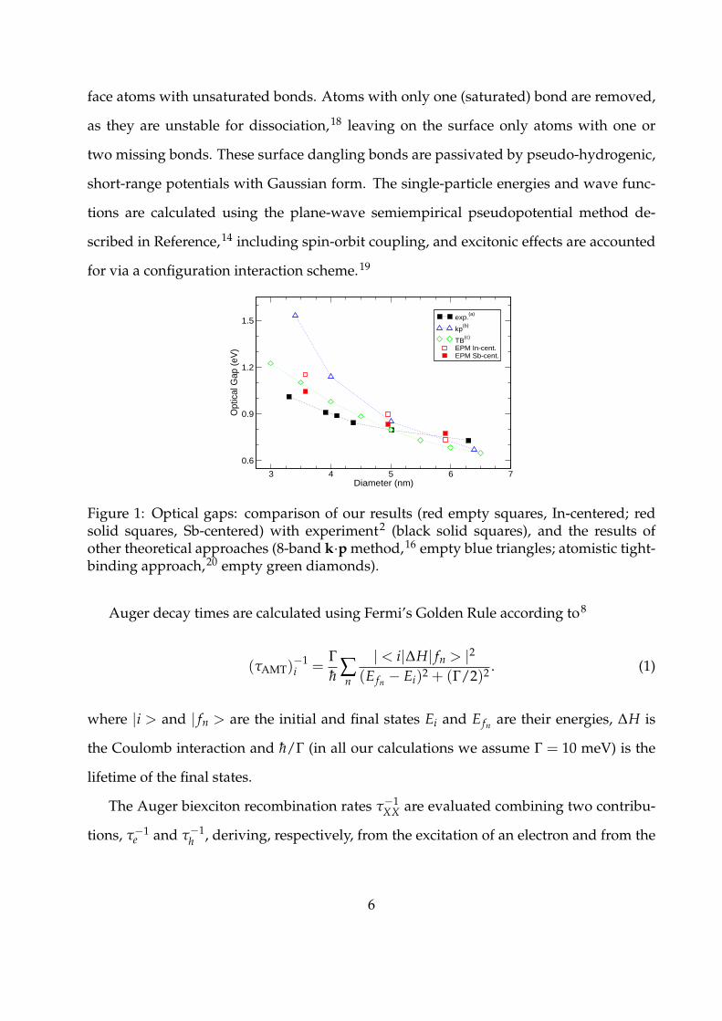
Figure 1: Optical gaps: comparison of our results (red empty squares, In-centered; redsolid squares, Sb-centered) with experiment2 (black solid squares), and the results ofother theoretical approaches (8-band k·pmethod,16 empty blue triangles; atomistic tight-binding approach,20 empty green diamonds).
Auger decay times are calculated using Fermi’s Golden Rule according to8
(τAMT)−1i =
Γ
h ∑n
| < i|∆H| fn > |2
(E fn − Ei)2 + (Γ/2)2. (1)
where |i > and | fn > are the initial and final states Ei and E fn are their energies, ∆H is
the Coulomb interaction and h/Γ (in all our calculations we assume Γ = 10 meV) is the
lifetime of the final states.
The Auger biexciton recombination rates τ−1XX are evaluated combining two contribu-
tions, τ−1e and τ
−1h , deriving, respectively, from the excitation of an electron and from the
6

excitation of a hole as:12
τ−1XX = τ
−1e + τ
−1h . (2)
1
1.5
2
2.5
78/21/1
21/69/10
1/82/17
37/59/4
29/66/5
44/41/15
50/35/15
/D = 2.1 nm
x2x2
x2
Γ XL/
81/11/8
53/38/9
52/41/7
25/67/8
27/65/8
50/38/12
Γ
D = 3.6 nm
x2
x2
x2
/L X/
89/6/5
18/79/3
3/96/1
83/11/6
84/11/5
4/95/1x2
/
D = 4.9 nm
x2
Γ L X/
91/7/2
0/100/0
x2
73/26/1
/
D = 5.9 nm
x2
71/27/2
68/31/1
49/50/1
Γ L X/
x2
78/21/1
Ene
rgy
(eV
)
Figure 2: Conduction band electronic structure for 4 different Sb-centered dot sizes: eachpanel refers to a different value of the dot diameter D and displays energy levels (left-hand side) and k-vector decomposition (right-hand side). The different states are coloredaccording to their main character (Γ red; L blue; and X green) resulting from such a de-composition. Two-fold degenerate states are indicated by ’×2’.
In Figure 1, we compare the excitonic gap calculated for In-centered and Sb-centered
CQDs of different sizes with the experimentally measured optical gaps.2 It is apparent
that In-rich stoichiometries yield larger gaps than observed experimentally, for small
structures, whereas Sb-rich structures reproduce observation well for the range of sizes
considered. Figure 1 also includes the predictions of other theoretical approaches, the
continuum-like 8-band k·p method16 and the atomistic tight-binding approach.20 While
the latter calculations (obtained for anion-centered structures) yield good agreement with
experiment, the agreement achieved by the former approach is only good in a very limited
size range. Most importantly, however, both theoretical curves (and our In-centered one)
cross the experimental curve, i.e. predict an increasingly lower gap than is observed for
sizes larger than about D=5 nm, a characteristic not exhibited by our Sb-centered results.
As the room temperature InSb bulk band gap at Γ is 0.180 eV,1 it would be reasonable to
7
expect the excitonic gap of the CQDs to converge to this value with increasing size, as the
predictions of k·p theory appear to do. However, the experimental gaps seem instead to
converge to a larger value, closer to the bulk band gap at L.2 The question therefore arises
of whether an indirect Γ-to-L transition is responsible for such a behavior in this size
range, as already found in the case of GaAs CQDs.3 If that were the case, since bulk InSb
has a direct band gap, the conduction band of the observed dots should have a prevalent
L character and should undergo an L-to-Γ transition at some large size above the experi-
mentally explored range. In order to shed light on this interesting issue, we performed a
k-space decomposition of the conduction band (CB) wave functions, following a similar
procedure as in Ref.,3 with the difference that here we use the high symmetry points Γ, L
and X as seeds for a Voronoi partition of the Brillouin zone,21 rather than using spheres
centered in those points. Each of the high-symmetry points is therefore associated with a
Voronoi cell in reciprocal space that has the property that each wave vector k in that cell
is closer to the specific high-symmetry point than to any other.
The latter choice is preferable, as the Voronoi cells, unlike spheres, have the same
symmetry as the nanostructure’s first Brillouin zone, and can therefore completely fill it
without overlapping.
As shown in Figure 2, the wave function of the CB edge receives a non negligible
contribution from the L point in the case of small dots. Such a component decreases with
increasing size, up to D = 5 nm and then increases again for D = 6 nm in Sb-centered
structures, whereas in In-centered dots the L component decreases monotonically (not
shown).
Interestingly we find that this trend is accompanied by a crossover between Sb-rich
and In-rich structures for Sb-centered dots. In fact, for sizes smaller than D = 6 nm,
Sb-centered nanostructures are also Sb-rich, whereas for D = 6 nm, the stoichiometry is
slightly reversed with a less than 1% excess of In atoms.
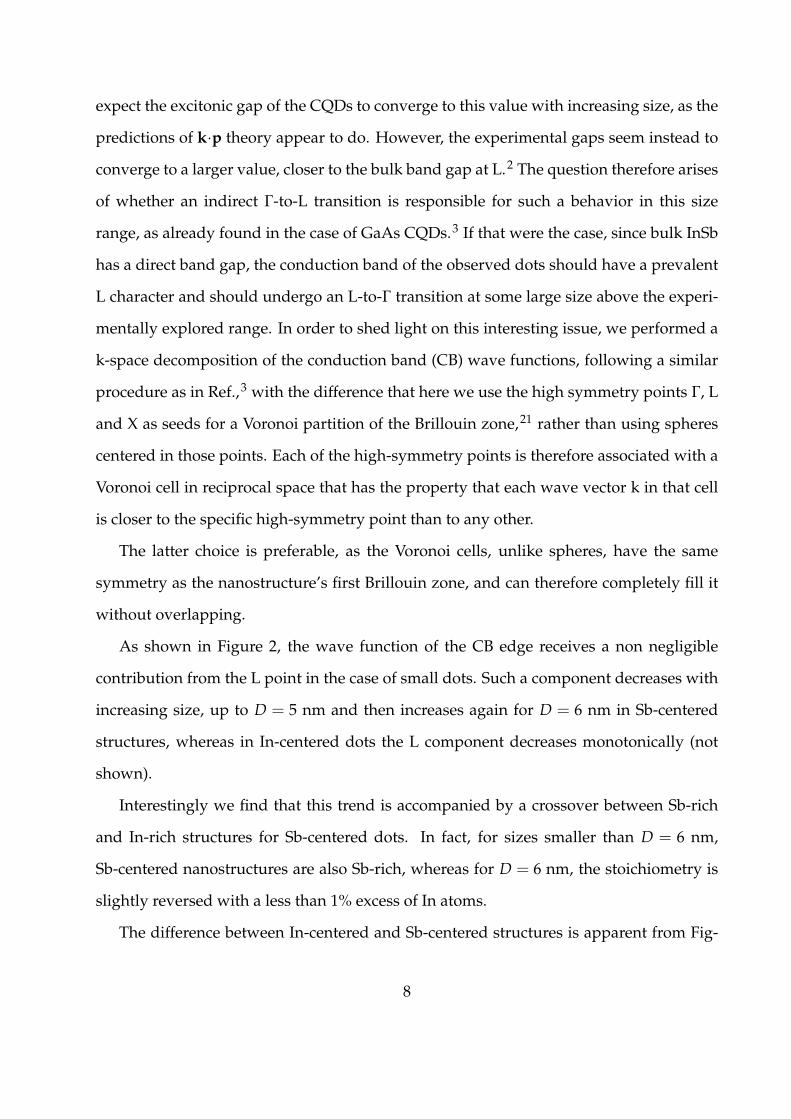
The difference between In-centered and Sb-centered structures is apparent from Fig-
8
In−centeredSb−centered
real space k−space
D = 5.9 nmD = 2.1nm
Figure 3: Real- and k-space representation of the CBM wave functions of D = 2.1 nm and5.9 nm dots for In-centered (blue) and Sb-centered (red) structures.
ure 3, where we compare the calculated real-space and k-space representations (i.e., the
charge density and the k-vector decomposition) of the CBM wave functions of the small-
est and largest dot considered in our study: although the k-vector composition in In-
centered and Sb-centered structures is similar for both sizes, the charge distribution is
clearly different, as a result of the different stoichiometries. This is especially evident for
D = 2.1 nm, where the relative difference in the number of atoms of the two species - 79
vs 68 - is significant. As a consequence of the mixed character of the CBM, the dot optical
gap is not expected to converge to the bulk band gap at Γ for sizes within the experimen-
tal window, consistently with observation. For larger sizes the L component is expected
to vanish and the gap to converge to 0.18 eV. Again it is worth stressing that the popular
8-band k·pmethod cannot predict this behavior, (unless new ad-hoc parameters are added
by hand to simulate this effect a posteriori), and that its predicted energy gaps underesti-
mate the experimental ones, for large R, despite the fact that (i) this approach is known to
overestimate confinement (hence the band gap) due to the assumption of an infinite confin-
ing potential,16 and (ii) its predicted p character for the VBM16 would imply absorption
to occur between VBM-2 and CBM, again leading to an overestimate of the band gap. Ac-
cording to our results, the VBM has instead prevalent s-like symmetry in both In-rich
and Sb-rich CQDs within the experimental size range, and therefore transitions between
9
2 3 4 5 6 7 8 9
Volume (10-26
m3)
0
5
10
15
20
25
Bie
xcito
n Li
fetim
e (p
s)
exp.(4)
theory
Figure 4: Biexciton recombination times as a function of dot volume: comparison of ourresults (red solid circles) with experiment4 (black solid squares). The dashed line is alinear fit through the experimental data.
band edge states are optically allowed. Interestingly, even an atomistic approach like
tight-binding fails to predict the correct behavior of the excitonic gap in CQDs with di-
ameters > 5 nm, perhaps owing to a too restricted choice of the basis set used,20 which
may limit the validity of the electronic structure description to regions near the Γ point.
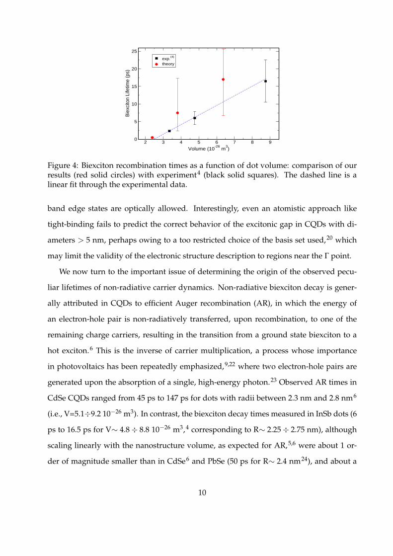
We now turn to the important issue of determining the origin of the observed pecu-
liar lifetimes of non-radiative carrier dynamics. Non-radiative biexciton decay is gener-
ally attributed in CQDs to efficient Auger recombination (AR), in which the energy of
an electron-hole pair is non-radiatively transferred, upon recombination, to one of the
remaining charge carriers, resulting in the transition from a ground state biexciton to a
hot exciton.6 This is the inverse of carrier multiplication, a process whose importance
in photovoltaics has been repeatedly emphasized,9,22 where two electron-hole pairs are
generated upon the absorption of a single, high-energy photon.23 Observed AR times in
CdSe CQDs ranged from 45 ps to 147 ps for dots with radii between 2.3 nm and 2.8 nm6
(i.e., V=5.1÷9.2 10−26 m3). In contrast, the biexciton decay times measured in InSb dots (6
ps to 16.5 ps for V∼ 4.8÷ 8.8 10−26 m3,4 corresponding to R∼ 2.25÷ 2.75 nm), although
scaling linearly with the nanostructure volume, as expected for AR,5,6 were about 1 or-
der of magnitude smaller than in CdSe6 and PbSe (50 ps for R∼ 2.4 nm24), and about a
10
3.5 4 4.5 5Diameter (nm)
0
0.2
0.4
0.6
0.8
1
1.2
1.4
Rel
axat
ion
Tim
e (p
s)
exp.(4)
theory
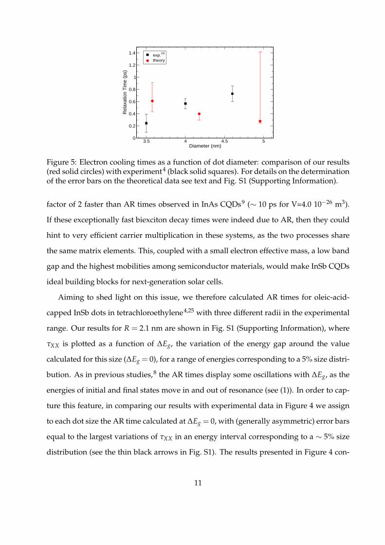
Figure 5: Electron cooling times as a function of dot diameter: comparison of our results(red solid circles) with experiment4 (black solid squares). For details on the determinationof the error bars on the theoretical data see text and Fig. S1 (Supporting Information).
factor of 2 faster than AR times observed in InAs CQDs9 (∼ 10 ps for V=4.0 10−26 m3).
If these exceptionally fast biexciton decay times were indeed due to AR, then they could
hint to very efficient carrier multiplication in these systems, as the two processes share
the same matrix elements. This, coupled with a small electron effective mass, a low band
gap and the highest mobilities among semiconductor materials, would make InSb CQDs
ideal building blocks for next-generation solar cells.
Aiming to shed light on this issue, we therefore calculated AR times for oleic-acid-
capped InSb dots in tetrachloroethylene4,25 with three different radii in the experimental
range. Our results for R = 2.1 nm are shown in Fig. S1 (Supporting Information), where
τXX is plotted as a function of ∆Eg, the variation of the energy gap around the value
calculated for this size (∆Eg = 0), for a range of energies corresponding to a 5% size distri-
bution. As in previous studies,8 the AR times display some oscillations with ∆Eg, as the
energies of initial and final states move in and out of resonance (see (1)). In order to cap-
ture this feature, in comparing our results with experimental data in Figure 4 we assign
to each dot size the AR time calculated at ∆Eg = 0, with (generally asymmetric) error bars
equal to the largest variations of τXX in an energy interval corresponding to a ∼ 5% size
distribution (see the thin black arrows in Fig. S1). The results presented in Figure 4 con-
11
firm that the biexciton decay times measured experimentally are indeed due to efficient
AR, opening the door for the exploitation of these nanostructures in photovoltaics.
Interestingly we find that AR times calculated for InAs and InSb dots of similar sizes
(R = 2.0 nm vs R = 2.1 nm, respectively) in similar conditions (i.e., with the same cap-
ping agents and in the same solution25), have similar magnitudes (i.e., they are the same
within the estimated error bars - compare red and green curves and red and green sym-
bols in Fig. S1). The difference observed experimentally4,9 may therefore be attributable
to surface and environmental effects.
Comparison between wurtzite CdSe dots with R = 1.92 nm and InSb dots with R =
1.78 nm, shows that the faster biexciton decay observed in the latter system may be at-
tributed to a combination of different factors: (i) the material’s crystal structure and (ii)
the small band gap of InSb. (i) Compared to the single excitation channel available,
upon non-radiative recombination of a ground state electron-hole pair, to the remain-
ing band edge charge carriers in wurtzite materials [|e1, e1;h1〉 → |en〉 for the electron and
|e1;h1,h1〉 → |hn〉 for the hole, see (2)], the two-fold degeneracy of the valence band maxi-
mum in zincblende materials provides twice as many channels for the electron excitation
[i.e., |e1, e1;h1〉 → |en〉 and |e1, e1;h2〉 → |en〉], and three times as many for the hole exci-
tation process [i.e., |e1;h1,h1〉 → |hn〉, |e1;h1,h2〉 → |hn〉 and |e1;h2,h2〉 → |hn〉]. (ii) Auger
coupling for the hole excitation process is found to be over two orders of magnitude
stronger in InSb (where it represents the most efficient decay) than in CdSe (where, in
contrast, τe is nearly a factor of 4 faster than τh, see (2)); the calculated AR matrix ele-
ments for the electron excitation process are instead only a factor of ∼ 6 larger in InSb.
We suggest the larger AR coupling to be a consequence of the smaller band gap of InSb,
leading to a larger overlap in this material, compared to CdSe, between the (final) excited
states involved in AR (which are located ∼ Eg away from the band edges and have there-
fore a higher kinetic energy and, likely, a higher charge density close to the dot surface in
CdSe than in InSb) and the (initial) band edge states (which are more localized within the
12

core). These arguments are supported by the fact that InAs CQDs, which have bandgaps
similar to InSb dots of the same size, and share the same crystal structure, also exhibit
similar calculated AR times.
Fast, but not unusual, electron intra-band decay times were also reported recently in
InSb CQDs4 and attributed to Auger cooling (AC), a non-radiative decay process inwhich
the excess energy of a hot electron is transferred, upon its decay to the conduction band
edge, to the hole, which is excited deep in the valence band.6 Our calculated AC times
are in agreement with experiment, as shown in Figure 5 (where the error bars have been
obtained following a similar procedure as in Figure 4), confirming that both non-radiative
decay processes observed in this material are Auger-like.
In summary, the application of the atomistic semiempirical pseudopotential method
to InSb CQDs has evidenced: (i) the s-like symmetry of their VBM in both In-rich and
Sb-rich structures, in contrast with the predictions of less sophisticated approaches; (ii) a
non-monotonic behavior of the L-component (i.e., the contribution from k-vectors close
to the L point in the Brillouin zone) of the CBM wave function with size, in Sb-centered
structures (not exhibited by In-centered CQDs), leading to (iii) an apparent failure of the
band edge absorption to converge to the bulk band gap, even for considerably large dot
sizes, consistent with observation, as the transition to a completely Γ-like CBM, and there-
fore a bulk-like band edge absorption, is expected to occur at a size close to the exciton
Bohr radius; (iv) the importance of the structure’s stoichiometry as a crucial input in the
calculations, as only considering the observed composition will lead to an accurate repro-
duction of the experimental data for both radiative and non-radiative decay processes;
(v) the unsuitability of continuum-like approaches to model InSb CQDs, as they lack the
necessary atomistic detail to capture (a) the crucial difference between Sb-rich and In-rich
structures of the same size, and (b) the details of the band structure away from Γ; (vi) the
Auger-like nature of the extremely fast biexciton decay, that suggests the possibility of
intriguingly high carrier multiplication yields in this system.
13
Acknowledgement
M.C. gratefully acknowledges financial support from the Royal Society under the URF
scheme. A.S.’s work was supported by a DTG from the EPSRC.
Supporting Information Available
Plot of τXX vs ∆Eg for InSb and InAs CQDs with R ∼ 2 nm. This material is available
free of charge via the Internet at http://pubs.acs.org.
References
(1) Group IV, Elements, IV-IV and III-V Compounds. Part b - Electronic, Transport,
Optical and Other Properties. In Landolt- BoÌLrnstein - Group III Condensed Matter,
Madelung, O.; RoÌLssler, U.; Schulz, M., Eds.; Springer-Verlag: Germany, 2002; Vol.
41A1b.
(2) Liu, W.; Chang, A. Y.; Schaller, R. D.; Talapin, D. V. Colloidal InSb Nanocrystals. J.
Am. Chem. Soc. 2012, 134 20258-20261.
(3) Luo, J.-W.; Franceschetti, A.; Zunger, A. Quantum-size-induced electronic transitions
in quantum dots: Indirect band-gap GaAs. Phys. Rev. B 2008, 78, 035306.
(4) Chang, A. Y.; Liu, W.; Talapin, D. V.; Schaller, R. D. Carrier Dynamics in Highly
Quantum-Confined, Colloidal Indium Antimonide Nanocrystals. ACS Nano 2014, 8,
8513-8519.
(5) Klimov, V. I.; Mikhailovsky, A. A.; McBranch, D. W.; Leatherdale, C. A.; Bawendi,
M. G. Quantization of Multiparticle Auger Rates in Semiconductor Quantum Dots.
Science 2000, 287, 1011-1013.
14
(6) Klimov, V. I. Optical Nonlinearities and Ultrafast Carrier Dynamics in Semiconduc-
tor Nanocrystals. J. Phys. Chem. B 2000, 104, 6112-6123.
(7) Pandey, A.; Guyot-Sionnest, P. Multicarrier Recombination in Colloidal Quantum
Dots. J. Chem. Phys. 2007, 127, 111104-1-111104-4.
(8) Wang, L.-W.; Califano, M.; Zunger, A.; Franceschetti, A. Pseudopotential Theory of
Auger Processes in CdSe Quantum Dots. Phys. Rev. Lett. 2003, 91, 056404.
(9) Schaller, R. D.; Pietryga, J. M.; Klimov, V. I. Carrier Multiplication in InAs Nanocrys-
tal Quantum Dots with an Onset Defined by the Energy Conservation Limit. Nano
Lett. 2007, 7, 3469-3476.
(10) Guyot-Sionnest, P.; Shim, M.; Matranga, C.; Hines, M. Intraband Relaxation in CdSe
Quantum Dots. Phys. Rev. B 1999, 60, R2181-R2184.
(11) Kambhampati, P. Hot Exciton Relaxation Dynamics In Semiconductor Quantum
Dots: Radiationless Transitions on the Nanoscale. J. Phys. Chem. C 2011, 115, 22089-
22109.
(12) Califano, M. Direct and Inverse Auger Processes in InAs Nanocrystals: Can the De-
cay Signature of a Trion Be Mistaken for Carrier Multiplication? ACS Nano 2009, 3,
2706-2714.
(13) Wang, T.; Vaxemburg, R.; Liu, W.; Rupich, S. M.; Lifshitz, E.; Efros, Al. L.; Talapin, D.
V.; Sibener, S. J. Size-Dependent Energy Levels of InSb Quantum Dots Measured by
Scanning Tunneling Spectroscopy. ACS Nano 2015, 9, 725-732.
(14) Wang, L.-W.; Zunger, A. Local-Density-Derived Semiempirical Pseudopotentials.
Phys. Rev. B 1995, 51, 17 398.
(15) Kim, D.; Kim, D.-H.; Lee, J.-H.; Grossman J. C. Impact of Stoichiometry on the Elec-
tronic Structure of PbS Quantum Dots. Phys. Rev. Lett. 2013, 110, 196802.
15
(16) Efros, A. L.; Rosen, M. Quantum Size Level Structure of Narrow-Gap Semiconductor
Nanocrystals: Effect of Band Coupling. Phys. Rev. B 1998, 58, 7120-7135.
(17) At D = 6 nm the dots are almost stoichiometric with the number of In atoms in the
cation-centered structures, however, lower than that of Sb atoms by 27 atoms out of
a total of 3181, and vice versa for the anion-centered structures.
(18) Kilina, S.; Ivanov, S.; Tretiak, S. Effect of Surface Ligands on Optical and Electronic
Spectra of Semiconductor Nanoclusters. J. Am. Chem. Soc. 2009, 131, 7717-7726.
(19) Franceschetti, A.; Fu, H.; Wang, L.-W. & Zunger, A. Many-body pseudopotential
theory of excitons in InP and CdSe quantum dots. Phys. Rev. B 1999, 60, 1819-1829.
(20) Sukkabot, W. Tight-Binding Theory of the Excitonic States in Colloidal InSb Struc-
tures. Mater. Sci. Semicond. Process. 2014, 27, 51-55.
(21) Aurenhammer, F. Voronoi Diagrams âAS A Survey of a Fundamental Geometric
Data Structure. ACM Computing Surveys 1991, 23, 345âAS405; Okabe, A.; Boots, B.;
Sugihara, K.; Chiu, S. N. Spatial Tessellations âAS Concepts and Applications of Voronoi
Diagrams. 2nd edition. John Wiley, 2000, ISBN 0-471-98635-6; Tran, Q.T.; Tainar, D.;
Safar, M. Transactions on Large-Scale Data- and Knowledge-Centered Systems, 2009, ISBN
9783642037214.
(22) Semonin, O. E.; Luther, J. M.; Choi, S.; Chen, H.Y.; Gao, J.; Nozik, A. J.; Beard, M.
C. Peak External Photocurrent Quantum Efficiency Exceeding 100% via MEG in a
Quantum Dot Solar Cell. Science 2011, 334, 1530-1533; Padilha, L. A.; Stewart, J. T.;
Sandberg, R. L.; Bae, W. K.; Koh, W.-K.; Pietryga, J. M.; Klimov, V. I. Carrier Multipli-
cation in Semiconductor Nanocrystals: Influence of Size, Shape, and Composition.
Acc. Chem. Res. 2013, 46, 1261-1269.
(23) Nozik, A. J. Quantum Dot Solar Cells.Physica E 2002, 14, 115.
16
(24) Schaller, R. D.; Petruska, M. A.; Klimov, V. I. Tunable Near-Infrared Optical Gain and
Amplified Spontaneous Emission Using PbSe Nanocrystals. J. Phys. Chem. B 2003,
107, 13765-13768.
(25) The presence of specific capping agents and solutions is accounted for by the appro-
priate choice of the dielectric constant outside the dot,8 in this case ǫ = 2.5.
17