Examination of Glass-Silicon andGIass- Glass Bonding ...
8
UCRL-JC-120533 PREPRINT Examination of Glass-Silicon andGIass- Glass Bonding Techniques for Microfluidic Systems N. F. Raley J. C. Davidson J. W. Balch This paper was prepared for submittal to 1995 Micromachining and Microfabrication Austin, TX October 23,1995 October 23,1995 This is a preprint of a paper intended for publication in a journal or proceedings. Since changes may be made before publication, this preprint is made available with the understanding that it will not be cited or reproduced without the permissionof .
Transcript of Examination of Glass-Silicon andGIass- Glass Bonding ...

UCRL-JC-120533 PREPRINT
Examination of Glass-Silicon andGIass- Glass Bonding Techniques for Microfluidic Systems
N. F. Raley J. C. Davidson
J. W. Balch
This paper was prepared for submittal to 1995 Micromachining and Microfabrication
Austin, TX October 23,1995
October 23,1995
This is a preprint of a paper intended for publication in a journal or proceedings. Since changes may be made before publication, this preprint is made available with the understanding that it will not be cited or reproduced without the permission of
.

. DISCLAIMER
Portions of this document may be illegible in electronic image products. Images are produced from the best available original document.
Examination of Glass-Silicon and Glass-Glass Bonding Techniques for Microfluidic Systems
N.F. Raley, J.C. Davidson and J.W. Balch
Lawrence Livermore National Laboratory Livermore, California 94550
ABSTRACT
We report here on the results of experiments concerning particular bonding processes potentially useful for ultimate miniaturization of microfluidic systems. Direct anodic bonding of continuous thin Pyrex glass of 250 pm thickness to silicon substrates gives multiple, large voids in the glass. Etchback of thick glass of 1200 pm thickness bonded to silicon substrates gives thin continuous glass layers of 189 pm thickness without voids over areas of 5 cm x 12 cm. Glass was also successfully bonded to glass by thermal bonding at 800 "C over a 5 cm x 7 cm area. Anticipated applications include microfabricated DNA sequencing, flow injection analysis, and liquid and gas chromatography microinstruments.
Keywords: bonding, polishing, glass, micromachining, microfluidics.
2. INTRODUCTION
There is much recent effort to form microfabricated fluidic analytical systems for chemical and biological applications using silicon micromachining technology. These devices often incorporate new requirements for the component structures. For example, thin glass on top of a silicon substrate using anodic bonding would be expected to allow fabrication of fluidic channels on the top surface of the glass with a degree of thermal and electrical isolation to the substrate and use of the silicon as a mechanical support or heatsink. A thick glass-glass thermal bond would allow thermal and electrical insulative encapsulation of the channel glass. One particularly important example is for DNA sequencing where the glass allows high voltage electrophoretic separation, adequate thermal conductance to a silicon heatsink, and ultraviolet probing and fluorescence of the separated components.
The new component structures often offer new and unexpected challenges for their fabrication. While anodic bonding of thick glass to silicon is a fairly routine procedure', thin glass bonding has not been extensively treated in the literature. Only recently, some reports of glass-glass bonding have appeared. In addition, some new microfluidic devices require these bonding processes to work over fairly large areas. Experimental considerations for the formation of these bonds are discussed in this paper.
3. EXPERIMENTAL,
For the anodically bonded structure, silicon was used as a substrate due to its widespread use in bonding to glass samples, its desirable mechanical and thermal properties, and its availability in large sizes. The general specifications of the silicon used were fairly standard at (100) orientation, single side polish, about 500 to 800 pm thick, and p-type dopant with 1-20 Q-cm resistivity. The surface roughness of the silicon was expected to be better than 50 nm with a total thickness variation of less than 10 pm.
All silicon samples used were rectangular in shape generated by scribing circular wafer discs. While most of the experiments reported here employed scribed 4 and 6 inch diameter wafers, a number of bonds were done starting with 8 inch diameter wafers as well. Even larger wafers up to 19 inches in diameter are readily available3.

Note that it is possible to obtain these rectangular silicon slices by cutting a silicon boule along its length instead of cross-section. However, vendors are not set up to polish rectangular slices uniformly and a large tooling cost is expected just to attempt the polish, without guarantee. It turns out that the cost per usable silicon area is expected to be as good or better using circular wafers and a subsequent rectangular scribe.
The glass samples used for all bonding experiments was Coming 7740 pyrex due to its common use in micromachining applications. A special glass advertised to be better thermally matched to silicon than Coming 7740 is available, but only in 1000 pm minimum thickness. The glass samples were generated by scribing 5 cm x 25cm rectangular pieces into sizes ranging from 5 cm x 5 cm up to 5 cm x 18 cm. The thiclcness of the glass used for the thin and thick glass bonding to silicon tests were about 250 pm and 1200 pm, respectively, while that used for the thermal self-bonding experiments was about 800 pm. The thickness variation for the thin glass was measured at about 39 pm while that for the thick glass was smaller at about 15 pm.
All samples for bonding were degreased with methanol and acetone, chemically cleaned in a 1 : 1 :5 solution of ammonium hydroxide, hydrogen peroxide and water at 70 "C for 10 minutes, and blown dry with nitrogen. The silicon samples also received a dip in a 1:50 solution of hydrofluoric acid and water for 10 seconds followed by water rinse to remove native oxide after the chemical clean.
The silicon and glass samples for anodic bonding were mounted on a tool steel baseplate in a cleanroom environment and subsequently placed in an oven for bonding. Electrodes were placed on top of the glass-silicon structure. The electrodes typically used were single or multiple square tool steel blocks with dimensions of 5 cm x 5 cm and 1.25 cm thick and weight equal to 230 g. The bonding voltage was transferred to the glass locally through bolts screwed in at the bottom comers of the blocks. The spacing of the electrode contacts was chosen so that the anodic voltage would be outside of a central region along the glass to allow, for example, fabrication of channels along the length of the glass. This was done in order to avoid potential glass pitting in the central region during bonding, especially observed at high temperature, presumed due to sodium hydroxide etching or electrical breakdown of the glass. In some tests, a modified electrode block was used with insulated through holes at the position of the bolts for voltage contact to the glass. This modification provided for additional direct weight contact over almost the entire bonding area while still localizing any pitting of the glass at the voltage contact points.
The anodic bonding oven used was an inert gas recirculation type with the chamber made from heavy-duty stainless steel. Nitrogen gas was flowmeter controlled in the chamber at a rate of about 12 lidmin. The typical pressure developed within the chamber at this flow was about 0.5 psi. It is expected that the temperature variation over a 10 cm x 30 cm sample area is controlled to better than 14 "C near the maximum oven temperature of 700 "C.
Most of the anodic bonds were performed at 550 "C using a constant current equal to 7 W c m ' to develop a maximum of 500 V electrostatic voltage. Some bonds employed temperatures as low as 300 "C and developed voltages as high as 1000 V. The voltage-time characteristic for typical bond experiments done at 550 "C is shown in Fig. I. A subsequent anneal at the bond temperature for about one hour was also performed. Etchback of thick glass on silicon was carried out on a grinding plate with temporary adhesive. Successive grinding steps were done to give a surface polish of about 1.0 to 5.0 MI.
The samples for glass-glass bonding were pressed together and then placed directly on a quartz boat or additionally supported on both sides with polished, 0.25" thick quartz plates to prevent warping. Some plates were roughened with grinding compound to give about 10 pm surface texture in order to prevent pyrex-quartz fusion. The bonding was carried out in a horizontal tube reactor with radiant heating for about one-half hour in nitrogen ambient at temperatures ranging &om 600 to 800 "C. This reactor was chosen for initial experiments due to its higher temperature capability compared to the anodic bonding oven available. However, the bonding results are not expected to depend on the heating mechanism, be it convection or radiation.

.#16 0#19
0
0.0 0.5 1.0 1.5 2.0 2.5 3.0
Time Q
Figure 1. Typical glass to silicon bond voltage characteristic as a bction of bond time at 550 "C.
30
= 550 "C 0 375 "C
c L. 0
-0 .d
0 0 1 2 3 4 5 6 7
Void diameter (mm)
Figure 2. Direct thin glass to silicon bond void height relation to void diameter for different bond temperature.
4. RESULTS
Initial attempts to anodically bond the thin glass to silicon resulted in small pieces of glass-silicon which broke away fiom the silicon substrate upon cooling, even at bond temperatures as low as 300 "C. This problem was resolved using glass from a different manufacturer and was' presumably due to a difference in thermal expansion coefficient between the two glasses. Samples as large as 5 cm x 12.5 cm were successfully fabricated.
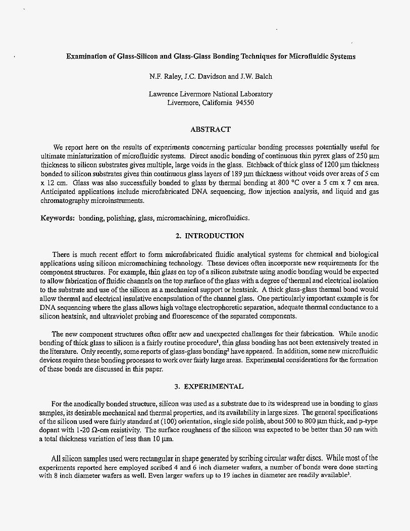
However, circular voids of various diameter were formed. The height of the voids was typically 10 pm for every 1 mm void diameter at a bond temperature of 550 "C as shown in Fig. 2. The area percentage of the voids was about 2.0 to 4.0 %. While the void height was reduced by bonding at 375 "C and the area percentage could be made lower using a higher developed voltage of 1000 V at 550 "C, the voids were nevertheless still present. Use of the modified electrode block to promote intimate contact did not help to eliminate voids. The void distribution was such that it would interfere with subsequent fabrication of structures in the glass, such as channels etched in glass along its length. This fact was substantiated by visual appearance which was quite unsatisfactoIy as shown in Fig. 3a.
Void formation, however, was negligible for thick glass bonded to silicon. Acoustic microscopy of the bonded area indicated a nearly perfect uniform bond. An alternative method to form thin glass on silicon, then, is to use etchback of thick glass. Initial attempt at etchback indicated no obvious cracks or warping of the thinned structure by visual observation after sample de-mounting and cleaning following grinding. The sample size was 5 cm x 12.5cm. The void-free characteristic typical of this structure is shown in Fig. 3b. A subsequent attempt to optimize glass thickness uniformity was made. The average glass thickness obtained was 189 pm with 60 pm variation or +15.9%. The thickness results are plotted in Fig. 4. This variation is comparable to commercially available rectangular thin glass of the same size with 39 pm thickness variation.
A summary of results for glass-glass bonding is shown in Table 1. It was found during initial attempts at glass- glass bonding that warping of the pyrex glass samples occurred at temperatures as low as 600 "C unless quartz plates were used for additional support over the entire area of the pyrex samples. In this case, it was then necessary that the surface of the quartz plate in contact with the pyrex be rough in order to prevent undesired bonding of pyrex to quartz, at least at 800 "C.
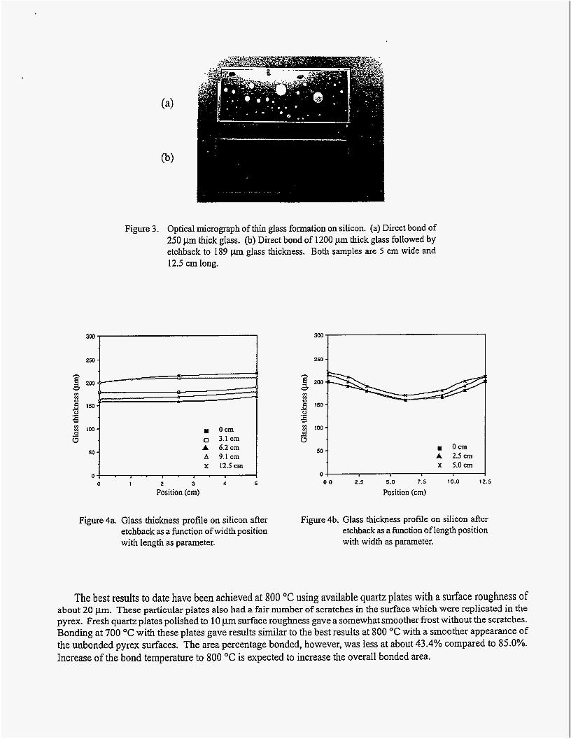
Figure 3. Optical micrograph of thin glass formation on silicon. (a) Direct bond of 250 pn thick glass. (b) Direct bond of 1200 pm thick glass followed by etchback to 189 pn glass thickness. Both samples are 5 cm wide and 12.5 cm long.
50 A 2.5 cm
5.0 cm
I c
3.1 cm
50
12.5 cm
0 1 2 3 4 5
Position (cm)
250 1 t I
Figure 4a. Glass thickness profile on silicon after etchback as a function of width position with length as parameter.
Figure 4b. Glass thickness profile on silicon after etchback as a function of length position with width as parameter.
The best results to date have been achieved at 800 "C using available quartz plates with a surface roughness of about 20 pm. These particular plates also had a fair number of scratches in the surface which were replicated in the Pyrex. Fresh quartz plates polished to 10 pn surface roughness gave a somewhat smoother frost without the scratches. Bonding at 700 "C with these plates gave results similar to the best results at 800 "C with a smoother appearance of the unbonded Pyrex surfaces. The area percentage bonded, however, was less at about 43.4% compared to 85.0%. Increase of the bond temperature to 800 "C is expected to increase the overall bonded area.

Temperature ("C)
600 600
/ 800 800 700
support Result
23.1 % edge bond, bowed 30.1% streak bond, flat 85.0% bond, rough surface Quartz-pyrex bond, cracks 43.4% bond, smoother surface
Table 1. Thick glass to glass bonding experiment summary.
5. DISCUSSION
The cause of the voids in direct anodic bond formation of thin glass to silicon is not entirely clear. Particulates which could conceivably prevent intimate bonding and lead to voids were not observed at the void locations. Bonding of thin glass samples with an array of holes gave much reduced void formation. Thick glass samples from either glass manufacturer were able to be bonded successfully without much problem with voids. Based on the reduced thickness variation for thick glass, it may be that its surface flatness is also better. This hypothesis is substantiated by the fact that few interference fringes were observed upon mounting of thick glass to silicon compared to thin glass. Thick glass is also rigid compared to thin glass which can be flexed.
The most likely explanation is that the degraded surface flatness and the more flexible nature of the thin glass compared to thick gIass is conducive to trapping air between the glass and silicon when mounted which leads to voids upon anodic bonding". Another possibility is that themally-induced relief of internal stress in the glass causes bowingS upon ramp to bond temperature which also promotes trapped gas (it should be noted in this regard that temperature variation over the sample is not a likely cause of voids by glass bowing since even small samples had voids where the expected variation was only 2 "C). Evolution of water or hydrogen fiom the glassS is an additional potential source of gas. It may also be that compressive stress induced in the glass upon formation of the depletion layer during bonding6 buckles the glass which prevents continued intimate contact as the bonding progresses once the bond temperature is reached.
Other solutions instead of etchback can be postulated to resolve void formation based on these mechanisms. Application of vacuum between the glass and silicon or a sequential sweep of bonding voltage across the sample may remove trapped air and promote more intimate contact if the degraded surface flatness of the glass is not too severe. The disadvantage of these techniques is increased complexity of the bonding apparatus and samples. Pre- anneal of the glass before bonding cycle is expected to relieve any internal stress as well as remove water in the glass. Occasional reversal of the voltage during bonding to replenish the depletion layer with ions may reduce buckling. Experiments to evaluate these potential solutions are in progress. The etchback technique, however, appears to be a viable method to form the thin glass-silicon structure.
AS concerns the glass-glass bonding results, a recent report2 indicates that borosilicate glass can bond to itself. Presumably, this effect is due to enhanced diffusion of glass component species at the interface at some fraction of the glass melting point. Based on the published melting point of boron doped glass as a fimction of the percentage of B,O, in SiO,7 and demonstration8 of bonding at 450 "C for an estimated B,O, percentage of 3 I%, the fraction of the glass melting point necessary for bonding is estimated to be about 0.50. Therefore, bonding is expected for 7740 pyrex glass with 13% B20, to occur at a temperature of 625 "C or higher. This estimation is consistent with published results2 which employ a bond cycle of 620 "C to 660 "C for 4 to 6 hours. The fact that the bonds observed here are obtained at higher temperature (700 "C to 800 "C) with shorter time (0.5 hour) supports the assumption that diffusion plays a role in the bond process. Further experiments are required to see if a glass-to-glass bond such as that demonstrated here can provide an effective seal to the thinned glass structure. This seal is expected to depend primarily on obtaining a suitably flat surface of the thin glass as a result of the etchback process.

6. CONCLUSIONS
An etchback technique of thick (1200 pm) pyrex glass anodically bonded to a rectangular silicon substrate has been successfully employed to form a thin (189 pm) continuous pyrex sheet on silicon over an area of 5 cm x 12.5cm without voids. Minimal void formation in thick glass bonds to silicon is ascribed primarily to negligible gas trapped between glass and silicon during mounting and possibly during the bond cycle. Glass-glass bonding has been achieved at 800 “C in nitrogen atmosphere with minimal bonding time according to a diffusion mechanism. These component structures are expected to have application to chemical and biological microinstruments.
7. ACKNOWLEDGMENTS
This work was performed under the auspices of the U.S. Department of Energy by the Lawrence Livermore National Laboratory under contract no. W-7405-ENG-48. The authors also wish to acknowledge T. Rodriguez, D.V an Lue, Y Sperry and B. Benett for anodic bonding hardware details and use of their oven in the initial stages of this work, B. Guthreau for parts fabrication, and M. Nichols for etchback work.
8. REFERENCES
[ 13 K.E. Petersen, “Silicon as a Mechanical Material”, Proceedings of the IEEE, vol. 70, no. 5, pp. 420-457, 1982.
[2] D.J. Harrison, K. Fluri, K. Seiler, Z. Fan, C.S. Effenhauser and A. Manz, “Micromachining a Miniaturized Capillary Electrophoresis-Based Chemical Analysis System on a Chip”, Science, vol. 261, pp. 895-897, 1993.
[3] Private communication, J. Boyle, Silicon Castings.
[4] C. Harendt, H.G. Graf, E. Penteker and B. Hofflinger, ‘Wafer Bonding: Investigation and In-Situ Observation of the Bond Process”, Sensors and Actuators, vol. A21-A23, pp. 927-930, 1990.
[5] T. Rogers, “Considerations of anodic bonding for capacitive type silicon-glass sensor fabrication”, J. Micromech. Microeng., vol. 2, pp. 164-166, 1992.
[6] Y Shoji, M. Yosida, K. Minami and M. Esashi, “Diode Integrated Capacitive Accelerometer with Reduced Structural Distortion”, Transducers ‘95, Stockholm, Sweden, pp. 581-584, 1995.
[7] “Handbook of Tables for Applied Engineering Science”, 2nd edition, R.E. Bolz and G.L. Tuve, editors, p. 163, 164, 339,341, CRC Press, Cleveland, Ohio, 1973.
[SI L.A. Field and R.S. Muller, “Fusing Silicon Wafers with Low Melting Temperature Glass’’, Sensors andrlctuators, V O ~ . A21-A23, pp. 935-938, 1990.