Evaluation Technology of Practical Electric Properties … · Evaluation Technology of Practical...
27
Evaluation Technology of Practical Electric Properties for High Frequency Materials Nov. 16 th , 2011 Tsukuba Research Laboratory Telecommunication Materials Development Center Printed Wiring Board Materials R&D Dept. Printed Wiring Board Materials Business Sector Yusuke Kondo, Hikari Murai Tetsuro Irino, Hiroshi Shimizu
Transcript of Evaluation Technology of Practical Electric Properties … · Evaluation Technology of Practical...

Evaluation Technology of Practical ElectricProperties for High Frequency Materials
Nov. 16th, 2011
Tsukuba Research LaboratoryTelecommunication Materials Development CenterPrinted Wiring Board Materials R&D Dept.Printed Wiring Board Materials Business Sector
Yusuke Kondo, Hikari MuraiTetsuro Irino, Hiroshi Shimizu

© Hitachi Chemical Co., Ltd. 2011. All rights reserved. 2
Freq
uenc
y ba
nd
Backplane
>10 Gbps(Optical/Electronic Interconnection?)
PCI(33 Mbps/ch, Parallel)
PCI-Express(2.5 Gbps/ch, Serial)
PCI-Ex.-H
(5 Gbps/ch, Serial)
HighHigh--speed digitalspeed digital(Server, Router,(Server, Router,HPC, etc) / HighHPC, etc) / High--
layerlayer
TACS/PDC:1G(800 MHz)
PDC:2G(1.5 GHz)
W-CDMA:3G(2 GHz)
ACC(24/60/76~79 GHz)
HSPA: 3.5G(2 GHz)
IMT-Advanced:4G(3~5 GHz?)
VICS (2.45 GHz)
GPS (1.5 GHz)
AHS (5.8 GHz)
ETC(5.8 GHz)
ITSMobile
3.9G:LTE(1.5 GHz)
RF/Wireless RF/Wireless ((Mobile, ITS, Mobile, ITS, WirelessWireless--LAN/Access, etcLAN/Access, etc))
Tran
smis
sion
spe
edCPU
Pentium IV(1.4~2.5 GHz)
Pentium III(0.45~1.3 GHz)
Pentium II(233~450 MHz)
Pentium(66~233 MHz)
Pentium IV/D(3.6 GHz)
Core2 Duo(2.66 GHz)
1990 2000 2010
Trend of high-Speed & high-frequency applications

© Hitachi Chemical Co., Ltd. 2011. All rights reserved. 3
Parallel Plate Capacitance
Whispering-Gallery Mode
SPPStrip Line Resonator
Cavity Resonator PerturbationDk/Df
10-3 10 20 30 40 50 1001Frequency [GHz]
Dielectric properties of materials
Practical electrical properties of PCB
Under planning
Under planning
Strip LineMicrostrip Line
Dk/Df, Attenuation
Transmissionloss (=ATT)+Environmental
test
Split Post Dielectric Resonator
10-3 10 20 30 40 50 1001Frequency [GHz]
Hitachi Chemical can satisfy various evaluation requirements
Hitachi Chemical's evaluation technology

© Hitachi Chemical Co., Ltd. 2011. All rights reserved. 4
Sampleform
Freq.
MethodSplit PostDielectric
ResonatorStrip LineResonator
Standard
1 ~ 20 GHz 1 ~ 30 GHz
・w/o conductor・Sheet / board・Thickness: ~ 0.5 mm
・Width: 10 ~ 130 mm
・Strip line・Thickness:≧1.0mm
・Characteristicimpedance:50 Ω
WG modedielectric resonator
50 ~ 100 GHz
・w/o conductor・Disk・Thickness: ~ 2 mm
・Diameter: 30 ~ 60 mm
IPC-TM-650 2.5.5.5.1JPCA-TM001-2007
CavityResonator
Perturbation
1 ~ 20 GHz
・w/o conductor・Stick・Thickness: ~ 1 mm
・Width: 1~2 mm・Length: 80 mm
JIS C-2565
Subject Material PCB
Under planning
・Various methods exist to evaluate dielectric properties of materials and PCBs.・Usable frequency band and sample form are different.
Evaluation methods of dielectric properties

© Hitachi Chemical Co., Ltd. 2011. All rights reserved. 5
Glass clothResin
・PCB materials have anisotropy because of difference of Dk betweenresin and glass cloth.
・Suitable methods are utilized to evaluate anisotropic dielectricproperties and practical electric properties of materials depending on frequency band and application of materials.
Electric field
Strip Line ResonatorSplit Post Dielectric Resonator
Electric field (occur on surface)
Glass clothResin
Trace
Anisotropy of PCB materials
© Hitachi Chemical Co., Ltd. 2011. All rights reserved. 6
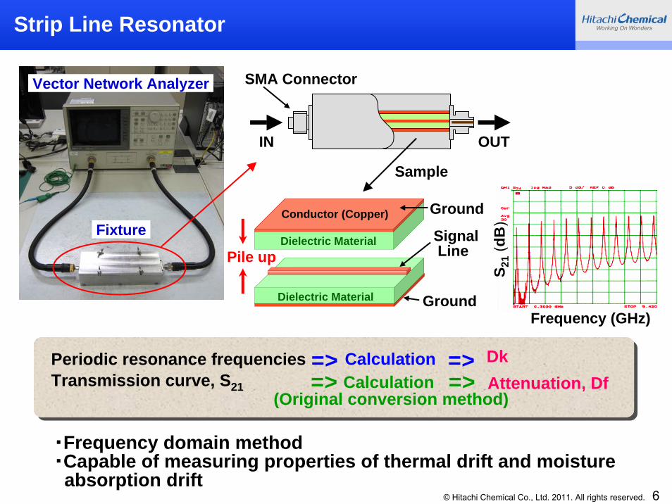
Vector Network Analyzer
Ground
Ground
SignalLine
Dielectric Material
Conductor (Copper)
Dielectric Material
Pile up
S 21
(dB
)
Frequency (GHz)
=>Periodic resonance frequencies DkTransmission curve, S21
CalculationAttenuation, DfCalculation
(Original conversion method)
IN OUT
SMA Connector
=>=> =>
Fixture
Sample
・Frequency domain method・Capable of measuring properties of thermal drift and moistureabsorption drift
Strip Line Resonator

© Hitachi Chemical Co., Ltd. 2011. All rights reserved. 7
< Measurement conditions >/ Method: Strip Line Resonator by Vector Network Analyzer/JPCA TM001/IPC-TM-650_2.5.5.5.1/ Temperature & humidity: 25 oC/ 60 %RH/ Laminate thickness: 0.8 mm (signal-ground distance: 0.8 mm), copper foil:18 μm/ Line width: 1 mm
2.5
3.0
3.5
4.0
4.5
0 2 4 6 8 10Frequency (GHz)
Dk
Conventional FR-4
FX-2
PTFE/E-glass
0
0.005
0.010
0.015
0.020
0.025
0 2 4 6 8 10
Frequency (GHz)
Df
Conventional FR-4
FX-2
PTFE/E-glass
Good stability of dielectric properties in wide frequency bands
Dielectric properties (vs. frequency)

© Hitachi Chemical Co., Ltd. 2011. All rights reserved. 8
0
0.005
0.010
0.015
0.020
0.025
0.030
0 1 2 3 4 5
PCT-Treating Time (h)
Df (
1 G
Hz)
3.03.23.43.63.84.04.24.44.64.85.0
0 1 2 3 4 5
PCT-Treating Time (h)
Dk
(1 G
Hz)
Conventional FR-4
FX-2
Conventional FR-4
FX-2
Stable Dk & Df against PCT treatment compared with FR-4
< Measurement conditions >/ Method: Strip Line Resonator by Vector Network Analyzer/JPCA TM001/IPC-TM-650 2.5.5.5.1/ Moisture treatment condition: PCT(121oC/0.22 MPa)-1~5 h/ Temperature : 25 oC/ Laminate thickness: 1.6 mm (signal-ground distance: 0.8 mm), copper foil:18 μm/ Line width: 1 mm
Dielectric properties (vs. moisture absorption)

© Hitachi Chemical Co., Ltd. 2011. All rights reserved. 9
0
0.005
0.010
0.015
0.020
0.025
0.030
-40 -20 0 20 40 60 80 100
Temperature ()
Df (
1 G
Hz)
3.0
3.2
3.4
3.6
3.8
4.0
4.2
4.4
-40 -20 0 20 40 60 80 100
Temperature ()
Dk
(1 G
Hz)
FX-2
Conventional FR-4 Conventional FR-4
FX-2
Good stability of dielectric properties against temperature
< Measurement conditions >/ Method: Strip Line Resonator by Vector Network Analyzer/JPCA TM001/IPC-TM-650 2.5.5.5.1/ Temperature: -30~90oC/ Laminate thickness: 1.6 mm (signal-ground distance: 0.8 mm), copper foil:18 μm/ Line width: 1 mm
Dielectric properties (vs. temperature)

© Hitachi Chemical Co., Ltd. 2011. All rights reserved. 10
FX-2 HE-679GResin rich,
PFResin poor,
LPResin rich,
RTFResin poor,
LP3.48 3.673.473.453.44
0.00540.00580.00620.0074
3.633.593.56
0.01480.01610.01650.0169
3.12 3.953 GHz 3.11 3.92
3.883.86
0.01150.01240.01250.0134
10 GHz 3.09
3 GHz 0.005310 GHz 0.005320 GHz 0.0064
20 GHz 3.090.0050
Category Frequency
1 GHz
Dk
1 GHz
Df
・Hitachi Chemical is certificated as an evaluator of SPP・SPP assessment is useful to accelerate R&D of materialsbecause we can know performance of materials including influence of copper foils
Test vehicle / SMASPP2z
SPP

© Hitachi Chemical Co., Ltd. 2011. All rights reserved. 11
Sampledisk
Dielectricwaveguides
Waveabsorber
VNA
Multiplier
HornAntenna
Waveguide tocoax transitions
Coaxialcables
Multiplier
Material Dk DfHE- 679G 4.16 0.0096LZ- 71G 3.68 0.0069
0.00390.01010.0078
FX- 2 3.52E- 700G(R) 4.61
3.91E- 800G(L)
Measurement system Resonance wave form
Dielectric properties (@60 GHz)
-50
-40
-30
-20
-10
0
50 55 60 65 70 75Freqency [GHz]
S21
[dB
]
Dielectric properties can be measured in millimeter wave band
Whispering- Gallery Mode Dielectric Resonator

© Hitachi Chemical Co., Ltd. 2011. All rights reserved. 12
Test board (up to 40 GHz)Test board (up to 20 GHz)
Connector
Coaxial cable
Test board
VNA
Probe station
VNA
Test board
Measurement of Strip line
Evaluation of PCB (SL)

© Hitachi Chemical Co., Ltd. 2011. All rights reserved. 13
180~200 μmCu:18 μm
100 μm100 μm
GNDSignal
GND
4 layers
ProbesTerminals
-4.0
-3.0
-2.0
-1.0
0.0
0 10 20 30 40Frequency(GHz)
Tran
smis
sion
loss
(dB/
cm)
Capable of evaluating strip line up to approximately 40 GHz
<Measurement condition>/ Structure: strip line/ Equipment: VNA/ Calibration:TRL
Connectoravailable Probe
available
Transmission loss of Strip line

© Hitachi Chemical Co., Ltd. 2011. All rights reserved. 14
Evaluation system for semi-microwave ~ milliwave properties
VNA
Probe station
Cross section of TEG
TEG PWB for evaluation (microstrip line structure)
S21
S11
Pattern for S11Measurement terminal
Pattern for S21
Evaluation of PCB (MSL)

© Hitachi Chemical Co., Ltd. 2011. All rights reserved. 15
Transmission loss (1~90GHz, S21@MSL)
< Measurement conditions >/ Structure: microstrip line/ Temperature & humidity:
25/40%RH/ Characteristic impedance: 50 Ω/ Calibration: TRL/ Dimension parameters・Line width(w): 0.2~0.22 mm・Dielectric thickness(b):
0.1~0.13 mm・Copper thickness(t): 18 μm・Line length: 10 mm & 20 mm ・Surface treatment of copper:
Ni(4 μm)/Au(0.5 μm) plating
wbt
Copper foil (15 μm)+Ni(4 μm) / Au(0.5 μm)
-1.8
-1.6
-1.4
-1.2
-1.0
-0.8
-0.6
-0.4
-0.2
00 10 20 30 40 50 60 70 8
Frequency (GHz)
Tran
smis
sion
loss
(dB
/cm
0 90
)
FX-2
Material R1 (Hydrocarbon/Ceramic)
Transmission properties

© Hitachi Chemical Co., Ltd. 2011. All rights reserved. 16
-7
-6
-5
-4
-3
-2
-1
0
-50 0 50 100 150Temperature ()
Tran
smis
sion
loss
(dB
/cm
@76
GH
z)
FX-2LZ-71GHE-679GE-67
-6
-5
-4
-3
-2
-1
0
0 10 20 30 40 50 60 70 80 90Frequency (GHz)
Tran
smis
sion
loss
(dB
/cm
)
-300256090120
<Measurement condition>/ Structure: microstrip line/ Equipment: VNA/ Calibration:SOLT
E-67(FR-4)
High frequency materials have good stability of transmission loss against temperature
100 μm
180~200 μm
Transmission loss (vs. temperature)

© Hitachi Chemical Co., Ltd. 2011. All rights reserved. 17
-0.02
0.00
0.02
0.04
0.06
0.08
0.10
0 500 1000 1500Processing time (hr)
⊿D
keff
(ca
lcul
ated
from
⊿ph
ase)
Influence of heat-processing
LZ-71G
Drift of Effective Dk can be evaluated in millimeter wave band
@76.5 GHz125oC / 1500hr
-180
-120
-60
0
60
120
180
0 20 40 60 80Frequency (GHz)
phas
e( o )
π
2/3π1/3π
-1/3π
-2/3π
-π
Pha
se (r
ad)
wbt
Copper foil (15 μm)+Ni(4 μm) / Au(0.5 μm)Effective Dk
Phase (vs. frequency)Drift
Effective Dk can be calculated from phase
・Line width(w): 0.2~0.22 mm・Dielectric thickness(b):
0.1~0.13 mm・Copper thickness(t): 18 μm・Line length: 10 mm & 20 mm ・Surface treatment of copper:
Ni(4 μm)/Au(0.5 μm) plating
Drift property of effective Dk (MSL)

© Hitachi Chemical Co., Ltd. 2011. All rights reserved. 18
-2.4
-2.0
-1.6
-1.2
-0.8
-0.4
0
0 200 400 600 800 1000 1200Processing time (hr/C-85/85)
Tran
smis
sion
loss
(dB
/cm@
76.5
GH
z)
Influence of humidity absorption
FX-2
FX-2
-40
-35
-30
-25
-20
-15
-10
-5
0
70 72 74 76 78 80Frequency(GHz)
S11(dB
)
InitialDrift
-0.100
-0.050
0.00
0.05
0.10
0.15
0.20
0 200 400 600 800 1000 1200Processing time (hr/C-85/85)
⊿D
k(C
alcu
late
d fro
m ⊿
f)
Drift property of transmission loss and Dk (MSL)

© Hitachi Chemical Co., Ltd. 2011. All rights reserved. 19
・3D EM field solver (Ansys HFSS)・Circuit simulator (Agilent ADS)
/ Designing of measurement terminals for evaluation of transmission properties to W-band, 100 GHz
/ Guessing of electrical performance, combination of structures, and themost suitable materials
/ Guessing of dielectric drift properties, ⊿Dk, by fitting calculated resonance properties, S11, to measured S11
MSL SL
Measurementterminal
Resonance pattern
Simulation technology

© Hitachi Chemical Co., Ltd. 2011. All rights reserved. 20
Reliability of FX-2 (update)
© Hitachi Chemical Co., Ltd. 2011. All rights reserved. 21
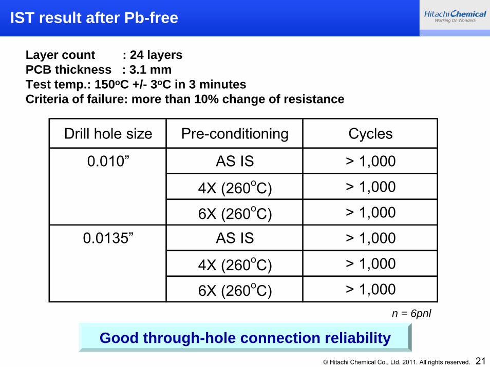
Layer count : 24 layers PCB thickness : 3.1 mmTest temp.: 150oC +/- 3oC in 3 minutesCriteria of failure: more than 10% change of resistance
Drill hole size Pre-conditioning Cycles
0.010” AS IS > 1,000
4X (260oC) > 1,000
6X (260oC) > 1,000
0.0135” AS IS > 1,000
4X (260oC) > 1,000
6X (260oC) > 1,000n = 6pnl
Good through-hole connection reliability
IST result after Pb-free

© Hitachi Chemical Co., Ltd. 2011. All rights reserved. 22
/ Total thickness: 4.1 mm (28 layer board)/ Wall-Wall Spacing: 0.40 mm,0.50 mm, about 2,000holes/ Precondition: 85oC/85%RH/120 h + Reflow 260oC X 10 times/ Measurement condition: 85oC/85%RH DC100 V/ The measurement of insulation resistance in chamber
Hitachi Chemical original pattern
CAF evaluation of high layer count board

© Hitachi Chemical Co., Ltd. 2011. All rights reserved. 23
Measurement condition: 85oC/85%RH DC100V, The measurement of insulation resistance in chamber
1.0E+001.0E+021.0E+041.0E+061.0E+081.0E+101.0E+12
0 100 200 300 400 500 600Treating time (h)
Insu
latio
n re
sist
ance
(Ω
)
1.0E+001.0E+021.0E+041.0E+061.0E+081.0E+101.0E+12
0 100 200 300 400 500 600Treating time (h)
Insu
latio
n re
sist
ance
(Ω
)
Wall-Wall Spacing:0.5 mm
Wall-Wall Spacing:0.4 mm
Good CAF restraining property
Results of CAF evaluation

© Hitachi Chemical Co., Ltd. 2011. All rights reserved. 24
<Measurement condition>/ Structure: Strip line/ Equipment: VNA/ Calibration:TRL 100 μm
100 μm
Line width:180~200 μmCu thickness:18 μm
Equal to conventional FX-2
-1.0
-0.8
-0.6
-0.4
-0.2
0.0
0 5 10 15 20Frequency (GHz)
Tran
smis
sion
loss
(dB/
cm)
ModifiedConventional
Transmission loss of modified FX-2
© Hitachi Chemical Co., Ltd. 2011. All rights reserved. 25
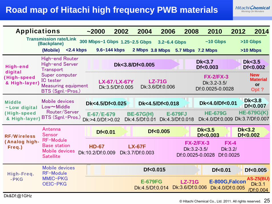
High-end RouterHigh-end ServerTransportSuper computerIC testerMeasuring equipmentBTS (Sgnl.-Pros.)
Transmission rate/Link(Backplane)
High-enddigital(High-speed& High-layer) LX-67/LX-67Y
Dk:3.5/Df:0.005LZ-71G
Dk:3.6/Df:0.006
Middle~Low digital(High-speed& High-layer)
E-67/E-679Dk:>4.0/Df:>0.02
FX-2/FX-3Dk:3.2-3.5/
Df:0.0025-0.0028
Applications
Mobile devicesLow~Middle
Router/ServerBTS (Sgnl.-Pros.)
RF/Wireless(Analog high-Freq.)
AntennaSensorRF-ModuleBase stationMobile devicesSatellite
HD-67Dk:10.2/Df:0.009
LX-67FDk:3.7/Df:0.003
(Mobile)
BE-67G(H)Dk:4.5/Df:0.01
HE-679GDk:4.0/Df:0.009
1.25~2.5 Gbps 3.2~6.4 Gbps ~10 Gbps >10 Gbps300 Mbps~1 Gbps
9.6~144 kbps<2.4 kbps 2 Mbps 3.8 Mbps
Opt ?Opt ?
HE-679G(K)Dk:3.7/Df:0.007
FX-2/FX-3Dk:3.2-3.5/
Df:0.0025-0.0028
E-679FJDk:4.3/Df:0.018
Dk<3.8/Df<0.005 Dk<3.7Df<0.003
New New MaterialMaterial
oror
Dk<4.5/Df<0.025 Dk<4.5/Df<0.018 Dk<4.0/Df<0.01
Df<0.01 Df<0.005 Dk<3.5Df<0.003
FX-4Dk:3.2/
Df:0.0025
~2000 2002 2004 2006 2008 2010 2012 2014
Dk<3.5Df<0.002
Dk<3.2Df<0.002
Dk<3.8Df<0.007
High-Freq.-PKG
Mobile devicesRF-ModuleMMIC-PKGOEIC-PKG
Df<0.015 Df<0.01 Df<0.005
E-679FGDk:4.5/Df:0.014
LZ-71GDk:3.6/Df:0.006
E-800G,FalconDk:4.0/Df:0.005
Dk&Df:@1GHz
ASAS--Z5(BU)Z5(BU)Dk:3.1
/Df:0.004
5.7 Mbps 7.2 Mbps >10 Mbps
Road map of Hitachi high frequency PWB materials

© Hitachi Chemical Co., Ltd. 2011. All rights reserved. 26
1. Hitachi Chemical has various evaluation technology ofdielectric properties and practical electrical properties.
2. Hitachi Chemical intend to accelerate R&D of materials for nextgeneration through these technology and newly constructedtechnology.
3. We also would like to propose the combination of the mostsuitable materials depending on PCB structure and applications by using evaluation technology and simulation.
Summary

© Hitachi Chemical Co., Ltd. 2011. All rights reserved. 27© Hitachi Chemical Co., Ltd. 2011. All rights reserved.