Evaluation of Si-LDMOS transistor for RF power amplifier …19163/FULLTEXT0… · ·...
89
Evaluation of Si-LDMOS transistor for RF power amplifier in 2-6 GHz frequency range Grigori Doudorov Reg nr: LiTH-ISY-EX-3435-2003 Linköping 2003
Transcript of Evaluation of Si-LDMOS transistor for RF power amplifier …19163/FULLTEXT0… · ·...

Evaluation of Si-LDMOS transistor for
RF power amplifier in 2-6 GHz frequency range
Grigori Doudorov
Reg nr: LiTH-ISY-EX-3435-2003Linköping 2003


Evaluation of Si-LDMOS transistor for RF power amplifier in 2-6 GHz frequency range
Master Thesis Division of Electronic Devices
Department of Electrical Engineering Linköping University, Sweden
Grigori Doudorov
Reg nr: LiTH-ISY-EX-3435-2003
Suprvisor: Qamar_ul_Wahab Examiner: Christer Svensson Linköping, Jun 05, 2003


Avdelning, Institution Division, Department
Institutionen för Systemteknik 581 83 LINKÖPING
Datum Date 2003-06-05
Språk Language
Rapporttyp Report category
ISBN
Svenska/Swedish X Engelska/English
Licentiatavhandling X Examensarbete
ISRN LITH-ISY-EX-3435-2003
C-uppsats D-uppsats
Serietitel och serienummer Title of series, numbering
ISSN
Övrig rapport ____
URL för elektronisk version http://www.ep.liu.se/exjobb/isy/2003/3435/
Titel Title
Utvärdering av Si-LDMOS transistorer för effektförstärkare i frekvensområdet 2-6 GHz. Evaluation of Si-LDMOS transistors for RF Power Amplifier in 2-6 GHz frequency range
Författare Author
Grigori Doudorov
Sammanfattning Abstract In this thesis the models of Si-LDMOS transistors have been investigated with Agilent EEsof ADS version 2002a for operation in the 2-6 GHz frequency range. The first one is the Motorola’s (MRF21010) model based on a 30 mm prototype of a Si-LDMOS transistor. The second one is a model based on a 1 mm prototype of Si-LDMOS transistor developed at Chalmers University. Large-signal simulations of Chalmers’ model have demonstrated results, which lead to the conclusion that, this model cannot be efficiently utilised for design for a PA in the 2-6 GHz frequency range. However, additional simulations with reduced Rd (drain losses) show the deep impact of this parameter on the main properties of the designed PA. Hence, it is important to take it into account during new processes of Si-LDMOS as well as to improve the CAD model. The final conclusion regarding Si-LDMOS cannot be made just based on these simulation results, since they are not in accordance with the published ones. The next step should be aimed at improving the model and further investigation of Si-LDMOS to prove their ability to operate in the 2-6 GHz frequency range.
Nyckelord Keyword LDMOS, RF, PA, output power, efficiency, linearity


i
Abstract In this thesis the models of Si-LDMOS transistors have been investigated with Agilent EEsof ADS version 2002a for operation in the 2-6 GHz frequency range. The first one is the Motorola’s (MRF21010) model based on a 30 mm prototype of a Si-LDMOS transistor. The second one is a model based on a 1 mm prototype of Si-LDMOS transistor developed at Chalmers University.
The models demonstrate simulated limitation for operation frequency either current gain (fT) or maximum available gain (fmax) at ~4 GHz and ~6 GHz respectively. However the models have been evaluated for higher frequencies to see the possibility for future improvement.
Regarding stability, Motorola’s model shows only conditional stability in the 2.1 – 2.23 GHz frequency range, hence the further investigation of Motorola’s model (MRF21010) was postponed.
Chalmers’ model demonstrates unconditional stability under all bias conditions and range of frequency.
Further, large-signal simulations of Chalmers’ model have demonstrated results, which lead to the conclusion that, this model cannot be efficiently utilised for design for a PA in the 2-6 GHz frequency range. However, additional simulations with reduced Rd (drain loses) show the deep impact of this parameter on the main properties of the designed PA. Hence, it is important to take it into account during new processes of Si-LDMOS as well as to improve the CAD model.
The final conclusion regarding Si-LDMOS cannot be made just based on these simulation results, since they are not in accordance with the published ones. The next step should be aimed at improving the model and further investigation of Si-LDMOS to prove their ability to operate in the 2-6 GHz frequency range.

ii

iii
Acknowledgements I would like to thank the people who have helped, supported and participated both in my work and studying time. First of all to Klas-Håkan Eklund and Christian Fager who have kindly provided me with Si-LDMOS model known as Chalmers` model in this thesis and gave me significant support throughout the whole work. Special thanks go to the people from Electronic Devices (EK) group (Linköping University) who made my work realisable:
• Christer Svensson for sharp ideas and advice and opening eyes at many things such as MOSFET, VLSI, etc.
• Stefan Andersson for valuable discussions about Amplifier’s noise, linearity, etc. issues
• Darius Jakonis for being my rumkamrat and solving many questions related to my work
• Jerzy J. Dabrowski for inspiring conversations regarding wide area telecommunication issues
• Arta Alvandpour for Computer support and Unix advice • Anna Folkeson for administrative support for my staying in the group • Peter Caputa, Kalle Folkesson, Joacim Olsson for helpful information and
discussions I would like specially to thank the people from the Department of Microwave Technology at the Swedish Defence Research Agency (FOI):
• Qamar ul Wahab, the best supervisor, who has given me an opportunity to participate in the process of technology development and helped a lot during my work
• Rolf Jonsson for advice, keeping track on my work, endless encouragement and support, language corrections, as well as for solving of simulations problems
• Aziz Ouacha for Microwave course and stability issues advice • Jonas Wissting for introducing me the non linear world of the active devices • Martin Hansson, Andreas Gustavsson and Mattias Alfredsson for advice
and discussions Moreover, I would like to thank all my friends, colleagues and relatives for support and believe in me: Igor Butylkin, Leonid Kalashnyk, Anastasiya Lundqvist, Jana Bekovska, Jonas Claeson, Diana Voitenko, Dmitriy Abramov, Ludmila Juchkova-Kuznechova, Marina Budaeva, Marija Komova, Andrew Smirnoff, Ekaterina Mitansina and many many others. Thank you very much my friends!
This work is devoted to my relatives and particularly to my lovely mother Vera...

iv

v
Table of contents 1 Introduction………………………..…………………………………… 1
1.1 Background…………………….……………………………………… 1
1.2 Outline of this thesis…………………………………………………… 1
1.3 Terminology…………………………………………………………… 2
2 Transistors……………………………………………………...…..…... 3
2.1 The basic types of transistors……………………….………….……… 3
2.2 Si-Lateral Double-Diffused MOSFET (Si-LDMOS)…………….…… 4
2.2.1 LDMOS features…………………………………….……...…… 5
2.2.2 RF properties of Si-LDMOS…………………….………..……... 6
2.2.3 Summary………………………………………………..……….. 6
3 Power Amplifier…………...………………………………………..….. 7
3.1 Amplifier’s building blocks………………………………………..….. 7
3.1.1 Bias Network and classes of PA……………………………..….. 8
3.1.2 Input/Output matching networks (IMN, OMN)……….……..….. 12
3.1.3 Accessories Networks (AN)……….…………………………..… 13
3.2 Properties of Power Amplifiers…………………………………..…… 13
3.2.1 Power, gain and efficiency…………………………………..….. 14
3.2.2 Linearity……………………………………………………..….. 17
3.2.3 Stability and noise……………………………………………..... 19

vi
4 Design, Simulation and Evaluation…………………….....………... 23
4.1 Device under simulation……...……………………………………..… 23
4.1.1 Available models of Si-LDMOS.………….…………………….. 23
4.1.2 Chalmers’ Si-LDMOS model for Agilent EEsof ADS…..………. 23
4.1.3 Motorola’s Electro Thermal LDMOS model………...….…….... 25
4.2 Design of PA……...…………….……………………..……………… 27
4.2.1 DC analysis.………….…………………………...…………….. 27
4.2.2 Small-signal (S-parameter) simulation.…..…………………… 29
4.2.3 Conclusion: small-signal analyses……………..………………... 31
4.2.4 Design and adjustment of matching networks (IMN, OMN)….….. 32
4.2.5 Large-signal analysis (Harmonic Balance) ……………………... 33
4.2.6 Load-pull analysis………………..…………………………….… 36
4.2.7 Conclusion: One-tone HB adjustment and Load-pull analysis.… 37
5 Results…………………………………………………………………... 39
5.1 Final result of simulations………………………………………….….. 39
5.2 Result of additional simulations……………………………………….. 39
6 Conclusion……………………………………………………………… 41
7 References……………………………………………………………… 43
Appendix A…………………………………………………………………. 45
Appendix B…………………………………………………………………. 49
Appendix C…………………………………………………………………. 55
Appendix D…………………………………………………………………. 59
Appendix E…………………………………………………………………. 65
Appendix F…………………………………………………………………. 69

vii
List of figures and tables
Figures
Figure 2-1 Basic types of transistors……………………………………….. 3Figure 2-2 Cross section of LDMOS……………………………………………….. 5Figure 3-1 Block diagram of an amplifier…………………………………………. 7Figure 3-2 Classes of power amplifier……………………………………………... 8Figure 3-3 Class-A IDS-VGS transfer characteristic……………………………….. 9Figure 3-4 Class-B IDS-VGS transfer characteristic……………………………….. 10Figure 3-5 Class-B IDS-VGS transfer characteristic……………………………….. 11Figure 3-6 Pout versus Pin, 1dB compression point………………………………… 16Figure 3-7 Two-tone intermodulation distortion…………………………………… 18Figure 3-8 Third order intercept point………………………………………………. 19Figure 4-1 (a) Simple LDMOS large-signal model [8]……….…………………... 24Figure 4-1 (b) Layout of Chalmers’ 1 mm LDMOS model….…………………... 25Figure 4-2 Large-signal Equivalent Circuit of the MET LDMOS model [14]…. 25Figure 4-3 Simple PA design flow………………………………………………. 27Figure 4-4 DC simulation setup……………………………………………………… 28Figure 4-5 Stability estimation simulation setup…………………………………… 29Figure 4-6 Unity current gain frequency (fT) simulation setup…………………… 31Figure 4-7 Small-signal optimization and adjustment…………………………….. 33Figure 4-8 One-tone simulation setup……………………………………………….. 34Figure 4-9 Two-tone simulation setup……………………………………………….. 35Figure 4-10 Load-pull simulation [15]……………………………………………….. 36 Figure A-1 (a,b) I-V characteristics of Chalmers’ model…………..……………... 45Figure A-2 (a,b) I-V characteristics of Motorola’s model………………..…….…. 47Figure B-1 S11 and S22 versus 2-6 GHz for Chalmers’ model……...…….……... 49Figure B-2 S11 and S22 versus 2-6 GHz for Motorola’s model……..…….…….. 52Figure C-1 (a,b)The set of stability factors for Chalmers’ model (28, 48V)…… 55Figure C-2 (a,b)The set of stability factors for Motorola’s model (28, 35V)...… 57Figure D-1 (a,b)Maximum available gain vs. frequency for Chalmers’ model… 59Figure D-2 (a,b)Maximum available gain vs. frequency for Motorola’s model... 60Figure D-3 (a,b)Current gain versus frequency for Chalmers’ model…………… 61Figure D-4 (a,b)Current gain versus frequency for Motorola’s model……......… 62Figure E-1 (a,b)Small-signal optimization results ……………….………………... 66Figure F-1 (a,b,c,d)One-tone harmonic balance simulationfor 2.4 GHz……….. 69Figure F-2 (a,b)One-tone harmonic balance simulationfor 3.2 GHz……….. 71Figure F-3 (a,b,c,d)Two-tone power sweep for 2.4 GHz and 3.2 GHz………….. 72Figure F-4 Deriving of the optimum load impedance (3.2 GHz) –example…….. 74

viii
Tables
Table 3-1 Classes of operation PA [9]……………………………………………... 12Table 4-1 One-tone harmonic balance adjustment results………..……………... 31Table 4-2 Comparison of the results for different approaches…...………...…... 37Table 5-1 Simulated results for different frequencies……………..……………... 39Table 5-2 Comparison of characteristics for Chalmers’ and Artificial models. 40Table A-1 The drain current versus bias conditions for Chalmers’ model…….. 46Table A-2 The drain current versus bias conditions for Motorola’s model……. 48Table B-1 (a,b)List of S-parameters for Chalmers’ model…...………………….. 50Table B-2 (a,b)List of S-parameters for Motorola’s’ model…….……………….. 53Table D-1 (a,b)Maximum available gain vs. frequency and VGS- Chalmer’s… 63Table E-1 (a,b)Source and Load impedances for simultaneous matching…….. 65

1
Chapter 1. Introduction
1.1 Background Silicon Laterally Diffused MOSFET (LDMOS) transistor is nowadays widely used in mobile base stations at 0.9 and 1.8(1.9) GHz due to its high power performance and linearity. The high RF output power is due to the new design for a higher DC breakdown voltage of typically 70-75V.
Recently Klas-Håkan Eklund group (consisting of Uppsala University and Eklund Innovation) has published modified LDMOS transistor structure showing even superior output power properties. The transistor showed a DC breakdown voltage in the range of 100-110 V. In terms of RF performance, the output power measured at 3.2 GHz was 1W/mm, which is today the highest compared to the Si and GaAs RF devices. These results are approaching to the wide band gap semiconductor devices (SiC and GaN). Due to the high breakdown voltage of 100 V, these devices have been operated as high as 70 V supply voltage. At this high drain voltage, a power density of more than 2W/mm is measured for the 1-mm device with a linear gain of 23 dB and maximum efficiency of 40% at 1 GHz frequency [4]. In the light of above measured results, it is desirable to evaluate the transistor performance in 2-6 GHz frequency range, where quite many applications exist for commercial (wireless telecommunications) as well as for military devices (radar, beam formers etc.)
1.2 Outline of this thesis
• Chapter 2 - Transistors: Brief overview of the main types of transistors and their definitions. The LDMOS is introduced.
• Chapter 3 - Power Amplifier: Operation classes and the typical and specific properties for a power amplifier.
• Chapter 4 - Design, Simulation and Evaluation: Introductory description of transistor models (Motorola’s and Chalmers’). The main part of the chapter is about the design flow and performed simulations.
• Chapter 5 - Results: Results description with additional simulation comparisons.
• Chapter 6 - Conclusion • Chapter 7 - References

Introduction
2
1.3 Terminology
AN: Accessories Network
BJT: Bipolar Junction Transistor
BN: Bias Network
CMOS: Complementary Metal Oxide Semiconductor
FET: Field Effect Transistor
GaAs: Gallium-Arsenide
GaN: Gallium-Nitride
HB: Harmonic Balance
HEMT: High Electron Mobility Transistor
IMD: InterModulation Distortion product(s)
IMN: Input Matching Network
IP: Intercept Point
LDMOS: Laterally Defused Metal Oxide Semiconductor
MAG: Maximum Available Gain
MESFET: MEtal Semiconductor Field Effect Transistor
OMN: Output Matching Network
PA: Power Amplifier
PAE: Power Added Efficiency
RF: Radio Frequency
Si: Silicon
SiC: Silicon-Carbide
UMOS: U-shaped gate Metal Oxide Semiconductor
VMOS: V-shaped gate Metal Oxide Semiconductor

3
Chapter 2 Transistors
This chapter gives the general description of the well-known types of transistors and presents a somewhat deeper understanding of a Si-LDMOS transistor. The basic types of transistors, which are widely used nowadays in different areas of electronics, are described in section 2.1. Section 2.2 gives an explanation of the contemporary Si-LDMOS together with its features and RF properties.
2.1 The basic types of transistors Transistors can be separated into two main groups: Bipolar and Unipolar. Bipolar Junction Transistors (BJT) use both electrons and holes as charge carries. Unipolar or Field-Effect Transistors (FET) operate only with one type of charge carriers. The BJTs are also called current-controlled devices, since the base current controls the collector current. On the other hand, in FETs the gate voltage controls the drain current through the device. Consequently, the FETs are voltage-controlled devices.
Figure 2-1 shows the different types of transistors such as Junction-FET (JFET), Metal-Oxide(Insulator)-Semiconductor-FET (MOSFET or MISFET) and MEetal-Semiconductor-FET or Schottky transistor (MESFET).
Figure 2-1. Basic types of transistors (the given structures illustrate NPN and n-channeldevices).
D-MOSFET
Basic types oftransistors
Bipolar Junction Transistors(BJT)
Field Effect Transistors(FET)
JFET MOSFET(MISFET)
E-MOSFET
n
p
n
C(collector)
E(emitter)
B(base)p
n
D(drain)
S(source)
G(gate)n
Insulator(SiO2)
p
n
D(drain)
S(source)
G(gate)n
Insulator(SiO2)
p
D(drain)
S(source)
G(gate)p
n-ch
anne
l
G(gate) s.i.
n+
D(drain)
S(source)
G(gate)n+
n
SemiinsulatedSchottky
contact
MESFET and HEMT

Transistors
4
There are two main types of the MOSFET: a depletion transistor - (D-
MOSFET) and an enhancement transistor - (E-MOSFET). The mostly used is E-MOSFET. There are many technologies such as low power CMOS, NMOS and power devices - LDMOS, VMOS, UMOS, which are based on the enhancement mode.
2.2 Si-Lateral Diffused MOSFET (Si-LDMOS) The lateral diffused metal-oxide-semiconductor transistor (LDMOS) was developed for RF applications in 1972 by Sigg [7]. Today it is intended to replace the convenient bipolar transistors in many telecommunication applications. The MOSFETs have several advantages over bipolar transistors. [6]:
• For high drain current, the MOSFETs have a high input impedance, and a low negative temperature coefficient.
• Thermally more stable FET cells combine better with each other than cells of bipolar transistors. This makes it easier to scale the active area when designing for high output power components. In addition, the good thermal stability of the MOSFET causes superior load-mismatch tolerance in comparison to the BJT.
• The MOSFET devices have lower intermodulation distortion (IMD) than bipolar transistors 1.
• In addition, due to quite low source inductance 2 MOSFETs have a higher power gain than bipolar transistors [6].
There are two general disadvantages of the MOSFETs. First, the gate is
sensitive to electrostatic charges 3. Second, at higher temperature the output power is reduced due to decreasing of transconductance [6].
The LDMOS is a representative of the Enhancement-Metal-Oxide-Semiconductor FET group. The different features and advantages of LDMOS (Figure 2-2) are discussed further.
1 Especially for the high order IMD products 2 Low source inductance is achieved due to a single bulk-source connection. 3 The sensitivity to electrostatic charges causes two problems: lowering of the threshold voltage and risk to destroy the device (electrostatic discharge).

5
Figure 2-2. Cross section of LDMOS [4],
p-substrate
n-drift region
n+
p-base
n+p+
n+ poly
Source
Gate Drain
channel regionsinker mµ3.0
mµ5.1
SiO2
2.2.1 LDMOS features The LDMOS could be seen as a transformed low power MOSFET transistor. There are several features, which improve RF and power properties of typical low power MOSFET transistors.
The LDMOS has a low doped and quite long n-drift region, which enhances the depletion region (Figure 2-2). The beneficial result of that is the improvement of the breakdown voltage. On the other hand the consequence of that is a higher on-state drain resistance, which degrades RF performance. The approaches to deal with a trade-off between the breakdown voltage and speed are discussed in [4].
The short channel of LDMOS is created by the lateral diffusion of a p-type implantation (p-base in Figure 2-2). Therefore, created by the lateral diffusion short channel region enhances RF performance 4.
The sinker principle is widely used for lateral power devices. The obvious advantage is in decreasing number of contacts that makes LDMOS easier to integrate. The bulk–source connection eliminates the extra surface bond wires. The RF performance of a such connection is better, because the source inductance is reduced. Therefore the device integration becomes much easier since there are only two contacts lefts, drain and gate [4,7].
4 In addition, in [7] the advantages of graded short channel region is discussed. Such as the prevention of the punch through, and improving the device transconductance.

Transistors
6
2.2.2 RF properties of Si-LDMOS The high-frequency properties of a Si-LDMOS transistor is usually determined by the length of the channel region. The shorter channel length improves the linearity since the transistor always works in velocity saturation [2].
GaAs based HEMT and MESFET are used in high frequency operation e.g. telecommunication applications. GaAs has higher saturation velocity compared to Si.
2.2.3 Summary Nowadays an interest is growing towards Si-LDMOS in telecommunication
area. Since Si is a developed material the structure of LDMOS gives both good high frequency and high power characteristics. The LDMOS still makes possible to keep its power gain, linearity and high output power in competitive values. The recent investigation shows an improvement in RF characteristics of Si-LDMOS, which surpass BJT and even approaches to SiC-MESFET performance [4]. For instance, the investigation of Si-LDMOS at 3.2GHz shows the output power over 30dBm (1W) with the drain voltage 50V. The efficiency has decreased compared to lower frequency, but the gain is still above 10dB with 1W/mm power density. Also 0.6W/mm is achieved at 28V supply voltage for 3.2GHz.
The aim of this work is to investigate the feasibility of the Si-LDMOS operation in the 2-6 GHz frequency range.

7
Chapter 3. Power Amplifier
In this chapter the power amplifier theory is described. The first section is about operation classes of amplifiers. The second describes the typical properties for a power amplifier (PA), such as output power, gain, efficiency and linearity. 3.1 Amplifier’s building blocks
The most convenient way for the evaluation of a power transistor is to design a class-A or class-AB Power Amplifier (PA). The design comprises several blocks for adjusting conditions for proper operation of the transistor(s) in accordance to the requirements. The main goal of this work is to investigate high gain, output power and linearity as general properties. The block diagram (Figure 3-1) represents a typical circuit considered in the design process. There are Bias Network (BN), Input Matching Network (IMN), Output Matching Network (OMN), Accessories Networks (AN) and the input and output ports that are assumed to be 50 Ohm.
Figure 3-1. Block diagram of an amplifier.
IMN OMN
BN
50Ohm
50Ohm
AN

Power Amplifier
8
3.1.1 Bias Network and classes of PA In order to operate a transistor for a certain class, the gate and drain DC voltages have to be biased carefully to the certain operation point (quiescent point or q-point). The reason is that the choice of q-point greatly influences linearity, power handling and efficiency. In addition, as can be seen further, the choice of optimal q-point is important for a certain operation frequency.
Figure 3-2 shows typical classes that are chosen according to specific requirements.
Figure 3-2. Classes of power amplifiers.
ID
VGSVGS(pinch-off)VGS (Threshold)
A
B
AB
0
…C
2(max)DI
(max)DI

Power Amplifier
9
Class-A Class-A is the most linear amplifier with the q-point biased close to half of the maximum drain current. The class-A amplifiers are also characterised by maximum possible conduction angle (2π) and rather low DC power efficiency (equal or less than 50% in theory). Figure 3-3 shows ideal transfer characteristic with biased q-point for class-A operation. The strongly non-linear effect (overdrive) occurs only when the drain current exceeds its saturation point (pinch-off) and/or gets into subthreshold region (cut-off).
Figure 3-3. Class-A Vgs- Ids transfer characteristic.
VGSVGS (Threshold)
Vgs Input waveform
Ids Outputwaveform
0
2(max)DI
(max)DI
DI
q-point
VGS(pinch-off)

Power Amplifier
10
Class-B For a class-B amplifier the operation point has to be selected at the threshold voltage to achieve high power efficiency (equal or less 78 % in theory). In a given case the linear characteristics drastically decrease due to the fact that the conduction angle is half as that for class-A (Figure 3-4).
VGSVGS(pinch-off)VGS (Threshold)
Vgs Input waveform
Ids Outputwaveform
0
2(max)DI
(max)DI
DI
q-point
Figure 3-4. Class-B Vgs- Ids transfer characteristic.
There will be current through the device only during half of the input
waveform (the positive part for the N-channel transistor). Hence, the input power capability of such a mode is almost twice as high.

Power Amplifier
11
Class-AB The class-AB amplifier shows a flexible solution for a trade-off between linearity and efficiency of the previous classes. In this mode the q-point has to be chosen in between A and B points with its exact place being a matter of application requirements. Therefore, the conduction angle is π-2π and typically chosen closer to the threshold voltage (Figure 3-5).
Figure 3-5. Class-AB Vgs- Ids transfer characteristic.
VGS(pinch-off)VGS (Threshold)
Vgs Input waveform
Ids Outputwaveform
0
2(max)DI
(max)DI
DI
q-point
VGS
Thus, the transistor response of class-AB is wider than for class-B due to the operation point. Also, the power efficiency is higher than for class-A. Many telecommunication applications utilize this mode. For example, it is widely used as a push-pull-AB amplifier for highly linear transmitters of cellular base stations.
There are also a number of very high efficiency non-linear amplifiers with reduced conduction angle such as C, D, F etc. They are not to be further considered in this work due to their very poor linear characteristics, which are outside purview of this work. In addition, their description can be found in [1,9].
Table 3-1 brings together comparisons for different classes in terms of quiescent point and conduction angle.

Power Amplifier
12
Table 3-1. Classes of operation PA [9] Class q-point (Vq) Quiescent current Conduction angle Max efficiency
A 0.5 0.5 2π 50 %
B 0 0 π 78 %
AB 0-0.5 0-0.5 π-2π 50 % - 78%
C < 0 0 0-π Approaches to 100 %
3.1.2 Input/Output matching networks (IMN, OMN) For most types of amplifiers a matching network is required to minimize so-called reflection (standing waves) problems. Matching networks are passive, consisting of striplines, inductors, capacitors and resistors. IMN and OMN provide proper transformation of impedance between source (50 Ohm) and the PA as well as between PA and load in order to achieve maximum gain and output power. There are three types of matching principles: 1) Conjugate matching The conjugate matching for the maximum gain is similar to what is issued in low noise amplifier (LNA) design. The IMN and OMN are adjusted to transfer source/load impedance (50 Ohm) toward device input/output impedance. By this method, theoretically, it is possible to achieve the maximum power gain and the minimum losses due to standing waves. In practice, during design it is important to consider the trade-off between the noise factor and the maximum achievable power gain. The conjugate matching is based on small signal S-parameter analysis. It is not effective for power amplifier, because the input signal cannot be treated as a small-signal. 2) Load-line matching The load-line method is explained by Cripps [9]. The general idea is based on load-line optimal resistance matching (Ropt), which provides highest output power. Therefore the OMN must translate the value Ropt of the device to load impedance (50 Ohm). The final formula to find Ropt is expressed as:
Ropt=(Vds-Vknee)/Imax, where (3.1) Vds is the supply voltage (28 V, 35 V or 48V in the current work), Vknee is the point where the current reaches saturation region when Vgs is constant and Imax is the maximum or saturation current. The design of input-matching network is similar to conjugate matching.
The theoretical result of loadline-matching design generally is 0.5-3 dB higher in 1dB compression point (P1dB) than the conjugate matching [9].

Power Amplifier
13
3) The matching based on Load Pull analysis This matching technique is based on a seeking of the optimal load impedance, which gives the convenient and flexible solution to solve a trade-off between efficiency and output power. The method from the very beginning utilised the relevant measurement equipment [9]. Recently it was implemented in the different CAD tools. For example, in Agilent EEsof ADS 2002a on the graph window the output impedances are plotted on the Smith chart that a result lead to values of gain and output power for each of them (Appendix F, Figure F-5). The Power and efficiency contours are generated empirically by the connecting various loads to the amplifier and by measuring the gain and the output power at each value of the load impedance [13]. The implemented Load Pull simulation in Agilent EEsof ADS is utilized in the current work (Chapter 4, Section 4.2.6).
3.1.3 Accessories Networks (AN) The accessories networks are different methods and facilities to improve
stability and linearity characteristics of the amplifier. To separate the natural behaviour of a transistor this project considers a simple model without any accessories networks.
The important thing regarding stability and frequency capability of the device is to check them before designing of the bias network. It is desirable to plot cut-off frequency (fT defined where the current gain is equal to 1) versus swept gate DC voltage (VGS) and to find the operation point where fT is as high as possible. In addition, the second step is to check for stability using different stability factors such as Rollett, Mason or Edwards [9,11].
3.2 Properties of Power Amplifiers The typical design aspects of an amplifier are listed below:
• Gain and gain flatness (dB)
• Output power (Watts or dBm)
• Operation frequency and bandwidth (Hz)
• Power supply requirements (V, A)
• Input and output reflection coefficients (VSWR)
• Noise Figure (dB) 5
5 It is not that important to consider Noise Figure for an PA.

Power Amplifier
14
The beneficial method is to characterise the properties through its two-dimensional scattering parameters matrix (S-parameters), which is widely used in RF/microwave theory. The importance of this method is derived from the fact that practical system characterisation can no longer be accomplished through simple open- or short- circuit measurement, as it is done for low-frequency applications (Z-, Y-, h-, and ABCD-parameters). This approach works very well under steady state and small-signal approximation. As it is known when dealing with power amplifiers this approximation is not valid because the amplifier operates over a nonlinear region. Therefore, some other techniques have to be obtained to conduct the appropriate design6. During this work Harmonic-Balance (HB) analysis is utilized as a method to characterise PA. Anyhow, small signal S-parameters may still be used when designing a class-A amplifier with sufficient precision. Here the signal amplification is largely restricted to the linear region of the transistor. However, the small-signal S-parameters become progressively unsuitable for class-AB, B, or C amplifiers, due to changing in the transfer characteristic of device (it is not possible to assume anymore, that transconductance is constant) [11]. In other words, when the power of the input signal reaches a certain level, the amplifier saturates and starts clipping the output signal. The consequence is the generation of spurious frequencies that invokes distortion the fundamental signal and power losses. As a result, the specific properties for evaluation of PAs as well as typical properties must be considered. 3.2.1 Power, Gain and Efficiency Power There are two concepts of power for RF/microwave circuits: available and dissipated power. Available or transferable is the maximum power, which is accessible from a source. The maximum available power is obtained from the source if the input impedance of the device equals the conjugate of the source impedance (Zin = Zs*) [13]. Therefore, for maximum available power as a function of frequency can be expressed as:
{ })(Re)(V
81)(
2S
ωω
ωS
av ZP = , where (3.2)
VS(ω) is a peak value of a sinusoidal voltage applied on input. Re{ZS(ω)} is the real part of the source impedance.
6 There are Large-Signal Scattering Parameters, Time-Domain (Transient) Analysis and Frequency-Domain Methods (Harmonic-Balance and Volterra-series analyses) are described in [13].

Power Amplifier
15
The dissipated or transferred power is the power dissipated in a load [13]. It can be expressed as:
{ })(Re)(V
21)(
2L
ωω
ωL
d ZP = , where (3.3)
VL(ω) is a peak value of a sinusoidal output voltage. Re{ZL(ω)} is the real part of the load impedance. The more practical representation for Output Power in terms of the classes of an PA is;
For class-A: maxmax,81
21 IVIVP Adcdcout == , where (3.4)
I max = 2Idc ; Vmax,A= 2Vdc are maximum drain current and voltage.
For class-B: maxmax,max1 81
41)(
21 IVIVtVIP BdcLout === , where (3.5)
I1 = 0.5Imax is is the fundamental component of the drain current, VL(t)=Vdc is the ac part of the drain voltage [13]. It is important to consider the value for different application requirements. For example, for IEEE802.11a,b,c the maximum linear output power must be 23-24 dBm. To characterize the PA the so-called power density parameter is frequently used. It is ratio between the power and transistor gate width (W/mm). The best results are achieved in [4] which shows 1-2 W/mm power density for Si-LDMOS. Gain There are different definitions of the gain. The most useful is transducer gain, which is the ratio between the power delivered to the load and the power available from the source. Transducer gain can be expressed by:
G= PL/PS , where (3.6) PS is the RF drive power and PL is the output RF power. The typical value of the transducer gain for a RF PA is 10-15 dB (assumed one-stage structure). The other useful definition is maximum available gain (MAG). Available gain is a ratio between the power available from the output of the transistor and the power available from the source. The maximum value is occurred when the input of the PA is conjugate-matched to the source. The MAG is the highest possible value of transducer gain in case when both the input and output ports are conjugate-matched. MAG can be defined only if the transistor

Power Amplifier
16
unconditionally stable7. It is also useful to evaluate the MAG versus swept frequency. It gives, so called, maximum frequency of oscillation (fmax), which shows the frequency when MAG reaches magnitude of 1 (0 dB). For the same reason, the current gain is evaluated versus frequency. The current gain is the short-circuit output current gain, which is a function of the swept gate voltage and the swept frequency. The value of the frequency, when the current gain drops to the magnitude of 1 (0dB), is called cut-off frequency (fT). 1 dB Gain compression point One of the crucial characteristics of power amplifiers is the so-called gain compression point. As the input signal to the amplifier approaches the saturation region, the gain begins to fall off or compress. The typical relationship between input and output power is shown in Figure 3-6.
Figure 3-6. Pout vs. Pin, 1dB compression point.
1 dB
Pin
Pout
Psat
IM33:1 slope
Pout1:1 slope
Linear Quasi-Linear Non-Linear
P1dB
At low drive levels, the output power is proportional to the input power. However, as the power goes beyond a certain point, the gain of the transistor decreases, and eventually the output power reaches saturation. The point where the gain of the amplifier deviates from the linear, or small-signal gain by 1 dB (about 1% distortion) is called the 1 dB compression point and it is used to characterize the power handling capabilities of amplifiers. The gain corresponding to the 1 dB compression point is referred to as G1dB and is 7 Only frequency and bias conditions, which conduct this statement, are considered in the current work [11].

Power Amplifier
17
computed as G1dB = G0-1dB, where G0 is the small-signal gain (or S21). Pout,1dB at the 1 dB compression point can be expressed in dBm if it is related to the corresponding input power Pin,1dB as:
Pout,1dB (dBm)=G1dB(dB)+Pin,1dB(dBm)=G0-1dB+Pin,1dB(dBm) (3.7)
Efficiency The operational efficiency of the amplifier can be estimated by the output efficiency (drain efficiency):
η= P1/Pdc, where (3.8)
P1 is fundamental output power expressed by P1=1/2VdcI1. Pdc is DC power consumption: Pdc=VdcIdc.
In addition, one of the frequently used parameters is Power Added Efficiency (PAE) expressed by:
PAE=(P1-PIN)/Pdc (3.9)
This parameter is particularly important from power-consumption and power- dissipation point of view. It is usually quantified in percentages. For example, for a class-A amplifier the transistor conducts during the whole wave period with an efficiency of 50% (in real life even less). It means that more than 50% of the energy dissipates as heat. It is not an acceptable condition for many telecommunication applications due to heating and battery lifetime issues.
3.2.2 Linearity Since a transistor is a nonlinear active device, the contemplation of its linearity characteristics must be taken into account. There are two well-known nonlinear effects. One is the weakly nonlinear effect and the other is the strongly nonlinear effect. For example, during analysis the linearity of LNA it is usually considered only weakly nonlinear effect [13]. However, this assumption is not acceptable for the PA due to relatively strong input signal. Therefore, both the nonlinear effects should be taken into consideration to obtain a successful design [9,13]. The key characteristics of linearity and harmonic balance as a method to characterize them for PAs are shown further.
Power Amplifier
18
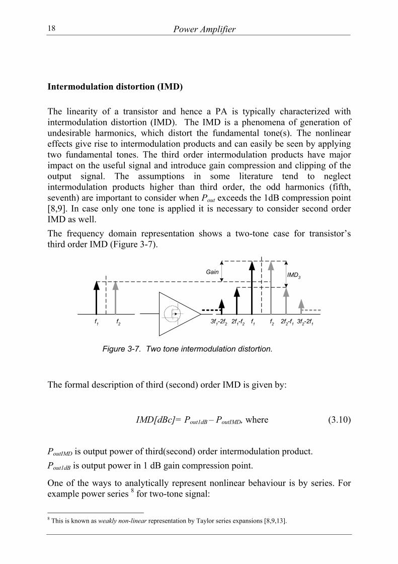
Intermodulation distortion (IMD) The linearity of a transistor and hence a PA is typically characterized with intermodulation distortion (IMD). The IMD is a phenomena of generation of undesirable harmonics, which distort the fundamental tone(s). The nonlinear effects give rise to intermodulation products and can easily be seen by applying two fundamental tones. The third order intermodulation products have major impact on the useful signal and introduce gain compression and clipping of the output signal. The assumptions in some literature tend to neglect intermodulation products higher than third order, the odd harmonics (fifth, seventh) are important to consider when Pout exceeds the 1dB compression point [8,9]. In case only one tone is applied it is necessary to consider second order IMD as well. The frequency domain representation shows a two-tone case for transistor’s third order IMD (Figure 3-7).
f1 f2 f1 f2
Gain IMD3
2f1-f2 2f2-f13f1-2f2 3f2-2f1
Figure 3-7. Two tone intermodulation distortion.
The formal description of third (second) order IMD is given by:
IMD[dBc]= Pout1dB – PoutIMD, where (3.10)
PoutIMD is output power of third(second) order intermodulation product. Pout1dB is output power in 1 dB gain compression point.
One of the ways to analytically represent nonlinear behaviour is by series. For example power series 8 for two-tone signal:
8 This is known as weakly non-linear representation by Taylor series expansions [8,9,13].

Power Amplifier
19
υ0=a1υi+a2υi2+a3υi
3+a4υi4+ a5υi
5+... etc., where (3.11)
υi= V1cos(ω1t)+ V2cos(ω2t) is the input waves (Figure 3-7) an is the gain for a certain order (the linear gain representation) Hence the third order intermodulation terms can be defined as:
)) cos(2 cos(2(4
3a12
221212
21
33 ωωωω −+)−= VVVVIMD (3.12)
Intercept point The other parameter to characterize linearity is the intercept point (IP). The point is shown in (Figure 2-8). If the 1:1 slope Pout versus Pin and the 3:1 slope IM3 versus Pin are extended, they will intersect at a point called IP3, the third order intercept point. IP3 is an approximation because the slope assumption is not truly valid outside the linear region. It is very useful to considered this point during design by component performance because the higher IP3 point, the less distortion at higher power levels.
Figure 3-8. Third order intercept point.
OIP3
Pin
Pout
Psat
IM33:1 slope
Pout1:1 slope
Linear Quasi-Linear Non-Linear
IIP3
IP3

Power Amplifier
20
Harmonic-balance analysis The Harmonic Balance (HB) analysis is refered as frequency domain method. The main reason to utilize HB in the current work, is that HB is most useful for strongly or weakly nonlinear circuits that have single or multitone excitation. HB is applicable to a wide variety of problems in RF/microwave circuits such as power amplifier, mixers and multipliers. HB calculates a circuit’s steady-state response. The One-tone and Two-tone harmonic-balance analyses are utilized in the current work, which are represented as one of the functional elements of Agilent EEsof ADS. A detailed description of HB can be found in [13].
3.2.3 Stability and noise
Stability
Generally, the reason of unstable behaviour of the active device is a reverse feedback from output to input.
There are several factors to estimate stability for class-A, -AB. The Rollett factor [9,11] is based on the two-port S-parameters matrix expressed as:
1221
2222
211
21
SSDSS
k+−−
= , where 21122211 SSSSD −= (3.13)
An alternative stability measure is given by the B1f -factor:
2222
2111 1 DSSB f +−+= (3.14)
For unconditional stability: k > 1, |D| <1 and B1f >0, otherwise the stability has to be taken into account 9. One of the graphical representations of stability are the stability circles [11]. It is a useful tool to avoid the unstable area when designing the matching networks with a Smith chart.
The solution to Instability [11]:
1. Choose a different device.
2. Change the bias conditions (only for class-A, -AB).
9 The k-factor, in fact, should not be too far from unity because devices with high k-factors also tend to have low gain. However some extra gain can be retrieved by additionally introducing positive feedback around the device, while keeping the k-factor above unity [9].

Power Amplifier
21
3. Avoid the instability region when matching.
4. Reduce the stage gain to stay within the maximum stable gain range.
5. Reduce the input and output impedance by resistive damping.
Noise The noise is defined with the Noise Factor (N). The Noise Factor is linear and equals the signal-to-noise ratio at the output divided by the signal-to-noise ratio at the input. Thus it is a figure of merit for how much noise that is added by the system itself. In the ideal case, when the system is completely noiseless the noise factor equals unity [11]. The Noise figure (NF) is an expression of the noise factor in dB.
Noise is less important for PAs, since it is the last active device in the transmitter building block chain. The Fries formula for the total noise factor for a cascaded system shows the importance of first stages.
12121
3
1
21 ...
1...
11
−⋅⋅−
++−
+−
+=n
ntot GGG
FGG
FG
FFF (3.15)
The last statement in this formula, typically, is for the PA. The gain from previous stages decreases the noise impact of the PA.

Power Amplifier
22

23
Chapter 4. Design, Simulation and Evaluation
In this chapter the simple PA design process performed using Agilent EEsof ADS is presented. The first section describes Si-LDMOS models utilized for Advanced Design System (Agilent ADS). The second section is about the feature of the performed design, simulation and evaluation as the main goal of the current project. 4.1 Device Under Simulation 4.1.1 Available models of Si-LDMOS
Two contemporary LDMOS models that were considered during this work. The first model is developed in Chalmers University and defined in [8]. This model is quite new and the data is based on a recently a developed LDMOS device [4].
The other is Motorola’s Electro Thermal (MET) LDMOS model [12]. However, the detailed description of this model has not been published, but a good explanation can be found in [14]. There are also several different LDMOS models such as Philips, Ericsson, Infineon and etc. Unfortunately, those models were not available during the time of this work. 4.1.2 Chalmers’ Si-LDMOS model for Agilent EEsof ADS One of the LDMOS models utilized in this work is based on the simple large-signal equivalent circuit shown in Figure 4-1. The concept and detail description are in [8]. The most critical elements of this model are described further.
Nonlinear Drain Current Model The nonlinear drain-current generator explained by the formula, which can be determined as a core of nonlinear behaviour of transistor. The current equation covers four operation regions. The first region is the subthreshold, where the drain current usually depends exponentially on the gate voltage. The second, where the voltage gets higher, the current rises quadratically – linear behaviour of the transconductance. The third region is because of the short channel effect

Design, simulation and evaluation
24
(velocity saturation), which gives linear dependence or the constant transconductance. The fourth, the transconductance will drop and the current will compress.
Figure 4-1(a). Simple LDMOS large-signal model [8].
Rg Rd
Rs
Cgs(Vgs’)
LdLg
Cds(Vds’)
Cgd(Vgd’)
Gate Drain
Ids(Vgs’,Vds’)
+
Vgs’
-
+
Vds’
-
+ Vgd’ -
Source
Drain access parasiticelements
Gate access parasiticelements
Source grounding accessparasitic elements
Intrinsic Large-signal FETmodel
Nonlinear Capacitances The proper modelling of nonlinear capacitances approaches the simulated results to the measured and reflects the large-signal and RF behaviour of the power transistor. This model has nonlinear capacitances without temperature effect, by assuming isothermal behavior of the device.
The equivalent circuit of this model (Figure 4-1) looks relatively simple10, however the simulated data show good accuracy with the measured ones regarding nonlinear behaviour of transistor [8]. The investigation for 1.9 GHz class-AB amplifier gives the interest to estimate this model for higher frequencies. The model based on the processed 1 mm device11 is shown in Figure 4.1(b). This model is simulated and analysed in the current work. The simplified cross section of one transistor gate is shown in Figure 2-2.
10 The self-heating effect is also included in this model by simple thermal R-C circuit, but has not been shown in Figure 4-1. 11 The 1 mm device includes 20 gate fingers with 0.05 mm (50 µm) width for each.

Design, simulation and evaluation
25
Figure 4-1(b). Layout of Chalmers’ 1 mm LDMOS model.
4.1.3 Motorola’s Electro Thermal(MET) LDMOS model The MET LDMOS model, is available as a library for many design tools such as Agilent EEsof ADS, AWR Microwave Office, APLAC Analog Design Tool, etc. [14]. The Motorola’s model is a commercialised one and its library include the whole row of LDMOS devices that has been recently developed and produced. The equivalent circuit of empirical large-signal MET LDMOS model is shown in Figure 4-2.
Figure 4-2. Large signal Equivalent Circuit of the MET LDMOS model [14].
Design, simulation and evaluation
26
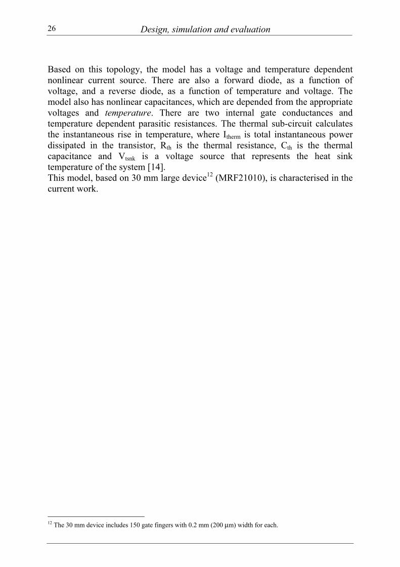
Based on this topology, the model has a voltage and temperature dependent nonlinear current source. There are also a forward diode, as a function of voltage, and a reverse diode, as a function of temperature and voltage. The model also has nonlinear capacitances, which are depended from the appropriate voltages and temperature. There are two internal gate conductances and temperature dependent parasitic resistances. The thermal sub-circuit calculates the instantaneous rise in temperature, where Itherm is total instantaneous power dissipated in the transistor, Rth is the thermal resistance, Cth is the thermal capacitance and Vtsnk is a voltage source that represents the heat sink temperature of the system [14]. This model, based on 30 mm large device12 (MRF21010), is characterised in the current work.
12 The 30 mm device includes 150 gate fingers with 0.2 mm (200 µm) width for each.

Design, simulation and evaluation
27
4.2 Design of PA The simple power amplifier circuits were designed in this work. The design flow is divided into seven fundamental steps and is shown in Figure 4-3:
Figure 4-3. Simple PA design flow.
Selection of a transistor model
I-V characteristics
Stabilityestimation
Cut-off (fT) freq.estimation
Small-signal (S-parameters) analysis
DC analyses
MAG and fmaxestimation
Adjust bias condition and Conjugate matching
Setup draft bias points
Result of evaluation
Large-signal (HB) analysis
P 1dB , Gain and IMP3 evaluation with one-, two-tone HB.
Adjust the output matching network
Load-pull simulation and analysis
Adjust the output matching network
Two- and one-tone harmonic balance analysis
Further, the set of schematics are obtained to fit the design flow in Figure 4-3. All simulations and analysis are performed using Agilent EEsof ADS ver.2002. 4.2.1 DC analysis The first step of design in the current work is to estimate the I-V characteristic. The results of these simulations decide about the first draft version of bias points.

Design, simulation and evaluation
28
DC simulations 1) Set-up The DC simulation was performed to depict the input/output I-V transfer characteristics. The I-V curves help to see, for example, the operation region of a transistor, the maximum drain currents, threshold voltage, knee region etc.
The built up circuit (Figure 4-4) has only bias networks with two DC voltage sources. The sources of the gate and the drain voltages are swept:
(a) For Chalmer’s model VGS =[0-5] V and VDS= [0-90] V. The results of simulation, I-V curves, are shown in Figure A-1 and Table A-1 (Appendix A).
(b) For Motorola’s model VGS =[2.5-8] V and VDS= [0-65] V. The results of simulation, I-V curves, are shown in Figure A-2 and Table A-2 (Appendix A).
Figure 4-4. DC simulation setup. 2) Results The performed simulations give the approximate values of bias networks for considered models:
Chalmers model: VGS = 0.8 – 3 V ; VDS= 28, 48 V. Motorola’s model: VGS = 3.3 – 4.2 V ; VDS= 28, 35 V.
As can be seen in Appendix A the models show rather different DC behavior. The Chalmers model has a variation of threshold voltage and maximum current for the considered drain voltages as:
VDS=28V -> VTH=1.0-1.1V , IMAX=155-158 mA VDS=48V -> VTH=0.8-0.9V , IMAX=139-141 mA
For the Motorola’s model the threshold approximately equal for both VDS: VDS=28V-> VTH=3.3-3.4V, IMAX=1.65-1.71 A
Design, simulation and evaluation
29
VDS=35V-> VTH=3.3-3.4V, IMAX=1. 54-1.64 A This difference is caused by channel length variation under different drain voltages. The input transfer characteristic (IDS-VGS) for 48(35) V drain voltage looks smoother and starts saturated earlier than for 28V.
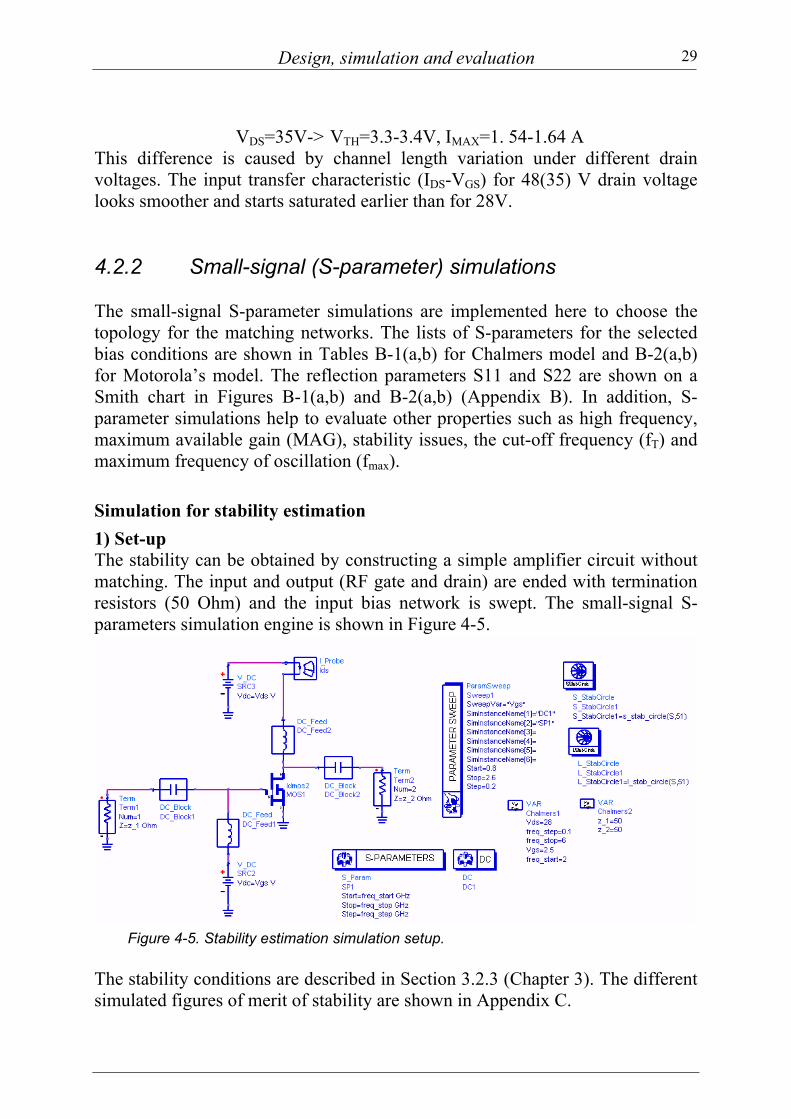
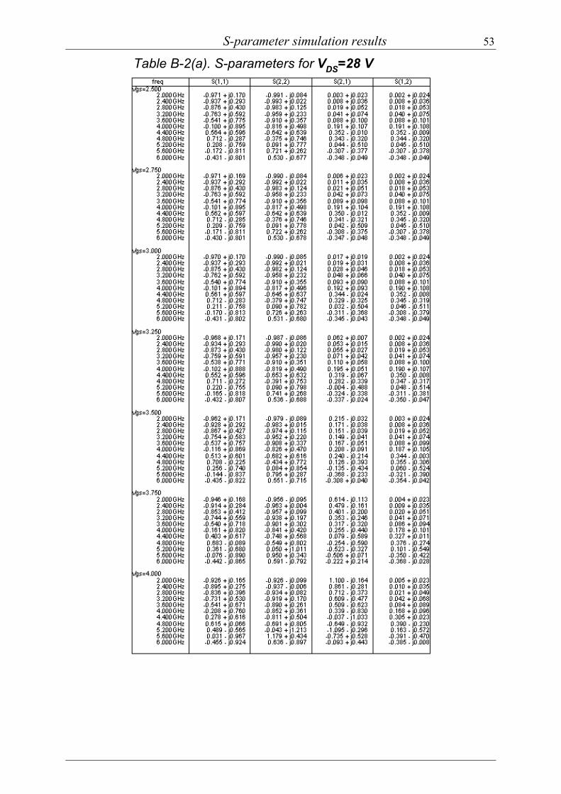
4.2.2 Small-signal (S-parameter) simulations The small-signal S-parameter simulations are implemented here to choose the topology for the matching networks. The lists of S-parameters for the selected bias conditions are shown in Tables B-1(a,b) for Chalmers model and B-2(a,b) for Motorola’s model. The reflection parameters S11 and S22 are shown on a Smith chart in Figures B-1(a,b) and B-2(a,b) (Appendix B). In addition, S-parameter simulations help to evaluate other properties such as high frequency, maximum available gain (MAG), stability issues, the cut-off frequency (fT) and maximum frequency of oscillation (fmax). Simulation for stability estimation 1) Set-up The stability can be obtained by constructing a simple amplifier circuit without matching. The input and output (RF gate and drain) are ended with termination resistors (50 Ohm) and the input bias network is swept. The small-signal S-parameters simulation engine is shown in Figure 4-5.
Figure 4-5. Stability estimation simulation setup.
The stability conditions are described in Section 3.2.3 (Chapter 3). The different simulated figures of merit of stability are shown in Appendix C.

Design, simulation and evaluation
30
2) Results The stability simulations show unconditionally stable operation for the Chalmers model during 2–6 GHz frequency range in Figure C-1 (a,b). For the same frequencies, the Motorola’s model does not fulfil the statement of unconditional stability and this fact must be carefully considered during further design. Maximum Available Gain (MAG) and maximum frequency of oscillation (fmax) analysis 1) Set-up This analysis depicts the maximum available gain versus frequency. Additionally, it can be seen when MAG becomes unity which is called maximum frequency of oscillation (fmax). The circuit for this simulation is the same in Figure 4-4. The result graphs and tables are in Appendix D. 2) Results As well as fT simulations, fmax help to find out the transistor’s frequency capability for different bias conditions. The MAG drops to 0dB around 5-6 GHz for both the models. Since the Chalmers model is unconditionally stable (see above) it can be taken into consideration as a limited frequency for this model. Different sources indicate that for the operation of the transistor for a given frequency to be warranted, it is desirable for the frequency fmax to be at least three or four times higher than the given frequency (in some literature even ten times). Despite of that fact, the represented models are considered further for the higher frequencies.
Cut-off frequency analysis (fT) 1) Set-up The next step is to build the circuit to estimate the cut-off frequency (fT). The bias networks are swept to depict fT when current gain reaches magnitude of 1 (0 dB). The utilized circuit is in Figure 4-6.

Design, simulation and evaluation
31
Figure 4-6. Unity current gain frequency (ft) simulation setup. The swept gate and drain bias voltages are applied to see behaviour of the current gain for different frequencies. The AC current source is swept in the 1.5 to 6.5 GHz frequency range. The results of the simulations for both models are shown in Figures D-3 and D-4 (Appendix D). So are the optimal values of VGS for particular VDS. 2) Results As can be seen in Figures D-3 and D-4, the capability from the current gain point of view frequency, both the models are around 4-5 GHz when the current gain reaches 0 dB. As well as for fmax, different sources indicate that for the operation of transistor for a given frequency to be warranted, it is desirable for the frequency fT to be at least two or three times higher than the given frequency. This statement shows that the frequency limit for the considered models are at least 2.5 GHz. However, the higher frequencies are considered in this work. 4.2.3 Conclusion: Small-signal simulations Chalmers’ model This model shows very stable behavior (unconditionally stable) in the 2-6 GHz frequency range. The graphs in Appendix C demonstrate the different factors, which prove unconditional stability of this model. The simulation for maximum frequency of oscillation shows variation of fmax by different gate biases. Therefore, the maximum value of fmax is possible to achieve in 1.8V gate bias point for both investigated drain voltages 28 and 48V (5.360GHz and 5.640GHz respectively).

Design, simulation and evaluation
32
The maximum values of fT are equal 3.950 GHz and 4.180 for 28V and 48V drain voltage respectively. The performed small-signal simulations indicate the operation frequency limitation for the model, yet it is not a convincing circumstance, that the real transistor is not valid for this frequency range. This fact is considered in the general conclusion of this work. Motorola’s model The small-signal characterization of this model shows the limitation for utilizing it for frequencies higher than 2230 MHz [12]. Figure D-4 (Appendix D) demonstrates current gain versus cut-off frequency. It is can be observed the strange behavior in frequency region higher than 3 GHz. The spike demonstrates huge current gain in approximately 4.7 GHz. This fact should be carefully considered, since it may by some additional “strange” parasitics effect due to model is prototype of packaged transistor. However, it also can be effect from very narrow adjusting of the model for the particular frequency range, below 2230 MHz.
4.2.4 Design and adjustment of matching networks (IMN,OMN) The S-parameters simulation generates a Smith chart and draws the input and output reflection parameters, S11 and S22, versus frequency. Appendix B presents the resulting Smith charts and tables with S-parameters for different frequencies. 1) Set-up The derived Smith charts provide a convenient approach to build the input and output matching networks [11]. The simple narrowband topologies of IMN and OMN are chosen in accordance to the location of S-parameters on the Smith charts as shown in Figure 4-7. The optimization and adjusting were performed to achieve a small-signal maximum transducer gain (in the ideal case it is equal to MAG). The optimizer engine in Agilent EEsof ADS is used. The goals for the engine were chosen as follows: OptimGoal1: S11: min=-150dB max=-13dB OptimGoal2: S22: min=-150dB max=-13dB OptimGoal3: S21: min= 20dB max= 50dB

Design, simulation and evaluation
33
Figure 4-7. Small-signal optimization and adjustment.
IMNOMN
IBN
OBN
2) Results Several frequencies were chosen for the evaluation of the models: 2.4GHz, 3.2 GHz, 3.6 GHz, 4 GHz, 4.8 GHz, 5.2 GHz. The different bias points were selected 13: VDS=28V, 48V -> VGS=1.165V, 1V. The Tables E-1(a,b) demonstrate the source and load impedances versus gate voltage for chosen frequencies. The performed adjustment is similar to the simultaneous conjugate matching approach described in [11]. In addition, the useful data in Tables D-1 (a,b) is given to compare the gain achieved by optimisation and MAG. As an example of adjustment, the small-signal gain (S21) are shown in Figure E-1(a,b) for 2.4 and 3.2 GHz respectively.
4.2.5 Large-signal analysis (Harmonic Balance) One-tone HB simulations The one-tone simulations in this work have two main goals. The first is to depict and analyze the gain, output power, and efficiency. The second is to perform 13 The selected bias points were derived as a optimal from load-pull simulations discussed in Section 4.2.6. The simulated results showed the best solution for trade-off between output power and efficiency.

Design, simulation and evaluation
34
additional adjustments of IMN and OMN in order to increase these properties. In other words, it is aimed to adjust previously designed matching networks for small-signal assumption to support the nonlinear (large-signal) assumption discussed in [8,9,11,13]. One-tone optimization and adjustment for the max output power and gain 1) Set-up The one-tone simulation (Figure 4-8) is used to find the maximum possible linear output power (P1dB) and gain. To do this the simulator adjusts the values of elements for matching networks (capacitors and inductances).
Figure 4-8. One-tone simulation setup.
IMN OMN
IBN
OBN
The goals are set as: OptimGoal1: P1db_out: min=35 dBm max=50 dBm OptimGoal2: Gain_1dB: min=15 dB max=25 dB As can be seen, the values aimed at are measured relative to 1 dB compression point. 2) Results The achieved results demonstrate improvement of output power or gain shown in Appendix F. In some examples, the output power was improved at the cost of a slight degradation in gain. It additionally demonstrates the trade-off between them, which is discussed in [9]. The Table below shows the results of output power and gain simulated after small-signal and one-tone HP adjustments (only for 2.4 and 3.2 GHz).

Design, simulation and evaluation
35
Table 4-1. One-tone HB adjustment results.
2.4 GHz VDS=28 V VGS=1.165V 3.2 GHz VDS=28 V VGS=1.165V P1dB [dBm] Gain [dB] P1dB [dBm] Gain [dB] Small-signal 23.878 6.463 Small-signal 22.449 2.059 One-tone HB 24.125 6.450 One-tone HB 22.640 2.042 VDS=48 V VGS=1.0V VDS=48 V VGS=1.0V P1dB [dBm] Gain [dB] P1dB [dBm] Gain [dB] Small-signal 26.391 7.846 Small-signal 24.223 3.430 One-tone HB 26.400 7.846 One-tone HB 24.328 3.393 Two-tone harmonic balance (HB) simulations The two-tone HB simulation is used to simulate the linear properties of the amplifier. The third order intermodulation distortion (IMD3) and IIP3 (OIP3) are discussed in Section 3.2.2 (Chapter 3). 1) Set-up The set-up circuit is similar to one-tone simulation and shown in Figure 4.9. The difference is the utilization of two-tone simulation engine. Two-tone signal with a spacing of 10 MHz are applied. The total power, which is applied on the input, is divided equally between the two tones. This power is shown in the set-up circuit as a “dbmtow(RFpower-3)” in logarithmic scale.
Figure 4-9. Two-tone simulation setup.
IMN OMN
IBN
OBN

Design, simulation and evaluation
36
2) Result The results of this simulation are shown in Appendix F. The two tones, input power versus output power and two tones IMD3 versus input power are shown in Figure F-3 (Appendix F) for different frequencies and bias conditions. Two 1dB compression points are demonstrated in figures; OTP1dB-one-tone 1dB compression points and TTP1dB- two-tone one dB compression points. 4.2.6 Load-pull analysis This analysis utilizes the built-in ADS load-pull circuit simulator. The idea is similar to that of the load-pull equipment, which is used for evaluation of a real device. Different values of load impedance are applied to find out the optimum one, which meets the required value of gain, output power and efficiency. The derived (simulated) value of the optimum load impedance is going to be utilized to adjust OMN. The adjustments are performed with help of simple LC network and two terminals. The goals set to transform the conjugated value of the simulated optimal impedance to 50 Ohm without losses (assumed in this work load and source impedance values are 50 Ohm). 1) Set-up The set-up of the load-pull simulation is shown in Figure 4-10. The simulation is performed for different bias conditions and frequencies are mentioned in Section 4.2.4.
Figure 4-10. Load-pull simulation [15].
Design, simulation and evaluation
37
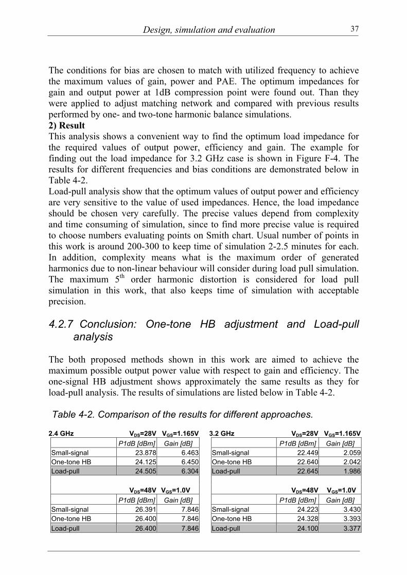
The conditions for bias are chosen to match with utilized frequency to achieve the maximum values of gain, power and PAE. The optimum impedances for gain and output power at 1dB compression point were found out. Than they were applied to adjust matching network and compared with previous results performed by one- and two-tone harmonic balance simulations. 2) Result This analysis shows a convenient way to find the optimum load impedance for the required values of output power, efficiency and gain. The example for finding out the load impedance for 3.2 GHz case is shown in Figure F-4. The results for different frequencies and bias conditions are demonstrated below in Table 4-2. Load-pull analysis show that the optimum values of output power and efficiency are very sensitive to the value of used impedances. Hence, the load impedance should be chosen very carefully. The precise values depend from complexity and time consuming of simulation, since to find more precise value is required to choose numbers evaluating points on Smith chart. Usual number of points in this work is around 200-300 to keep time of simulation 2-2.5 minutes for each. In addition, complexity means what is the maximum order of generated harmonics due to non-linear behaviour will consider during load pull simulation. The maximum 5th order harmonic distortion is considered for load pull simulation in this work, that also keeps time of simulation with acceptable precision. 4.2.7 Conclusion: One-tone HB adjustment and Load-pull
analysis The both proposed methods shown in this work are aimed to achieve the maximum possible output power value with respect to gain and efficiency. The one-signal HB adjustment shows approximately the same results as they for load-pull analysis. The results of simulations are listed below in Table 4-2. Table 4-2. Comparison of the results for different approaches.
2.4 GHz VDS=28V VGS=1.165V 3.2 GHz VDS=28V VGS=1.165V P1dB [dBm] Gain [dB] P1dB [dBm] Gain [dB] Small-signal 23.878 6.463 Small-signal 22.449 2.059 One-tone HB 24.125 6.450 One-tone HB 22.640 2.042 Load-pull 24.505 6.304 Load-pull 22.645 1.986 VDS=48V VGS=1.0V VDS=48V VGS=1.0V P1dB [dBm] Gain [dB] P1dB [dBm] Gain [dB] Small-signal 26.391 7.846 Small-signal 24.223 3.430 One-tone HB 26.400 7.846 One-tone HB 24.328 3.393 Load-pull 26.400 7.846 Load-pull 24.100 3.377

Design, simulation and evaluation
38

39
Chapter 5. Results
5.1 Final results of the simulations The simulations were performed for different narrowband conditions: 2.4 GHz; 3.2 GHz; 3.6 GHz; 4.0 GHz; 4.8 GHz; 5.2 GHz. The gate bias points were considered for class-AB amplifier (very close to class-B). The power supply (drain voltage) simulated for 28 and 48V. PA structures with simple narrowband matching networks were designed, simulated and analysed. The results of the simulations are showing the main properties for the considered frequencies in the table below (all data in the table are shown for bias condition: VDS=48V, VGS=1V).
Table 5-1. Simulated results for different frequencies
Frequency P1dB [dBm] Gain [dB] PAE[%] IMD3 [-dBc] 2.0 GHz 29 10.5 18 21 2.4 GHz 26 7.8 12 22 3.2 GHz 24 3 6.5 24 3.6 GHz 23 1.35 2.25 26 4.0 GHz 22 -0.69 -0.52 x 4.8 GHz 20 -5.12 -8.11 x 5.2 GHz 19.5 -7.35 -13.69 x
The table demonstrates the maximum values, which were achieved by optimisation of the matching networks designed PA for the maximum output power and gain. There are output power, gain and PAE, IMD3 for one- and two-tone simulation respectively. IMD3 is given for the input power in 1 dB compression point. The parameters degrade with higher frequency as expected. Particularly, the negative values of PAE and gain indicate that the power level of the fundamental output tone(s) is lower than it is for input tone(s). Thus, it is not amplifier anymore and the transistor has to be kept away from these frequencies of operation. The linear output power P1dB for example important telecommunication applications, shows acceptable value 23 dBm even for 3.6 GHz. The figure of linearity (IMD3) shows average third order intermodulation distortions about -22dBc for the frequencies with positive gain.
Results
40
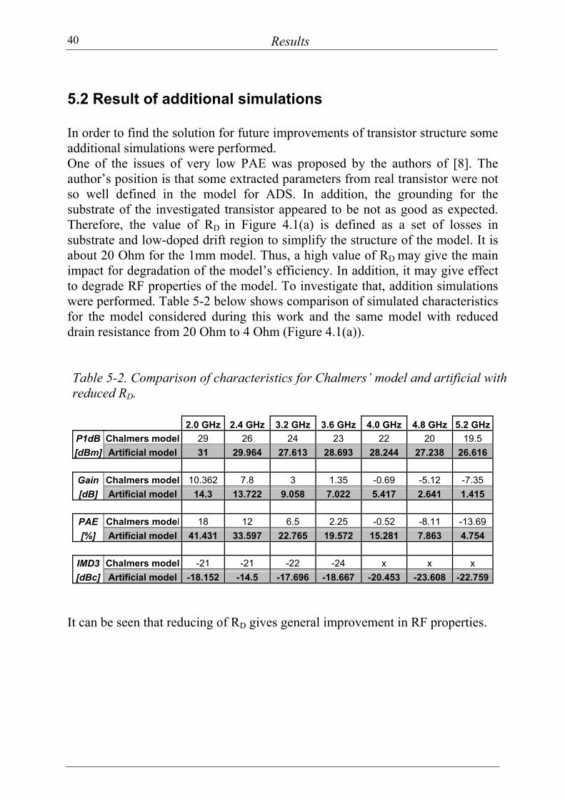
5.2 Result of additional simulations In order to find the solution for future improvements of transistor structure some additional simulations were performed. One of the issues of very low PAE was proposed by the authors of [8]. The author’s position is that some extracted parameters from real transistor were not so well defined in the model for ADS. In addition, the grounding for the substrate of the investigated transistor appeared to be not as good as expected. Therefore, the value of RD in Figure 4.1(a) is defined as a set of losses in substrate and low-doped drift region to simplify the structure of the model. It is about 20 Ohm for the 1mm model. Thus, a high value of RD may give the main impact for degradation of the model’s efficiency. In addition, it may give effect to degrade RF properties of the model. To investigate that, addition simulations were performed. Table 5-2 below shows comparison of simulated characteristics for the model considered during this work and the same model with reduced drain resistance from 20 Ohm to 4 Ohm (Figure 4.1(a)). Table 5-2. Comparison of characteristics for Chalmers’ model and artificial with reduced RD.
2.0 GHz 2.4 GHz 3.2 GHz 3.6 GHz 4.0 GHz 4.8 GHz 5.2 GHzP1dB Chalmers model 29 26 24 23 22 20 19.5 [dBm] Artificial model 31 29.964 27.613 28.693 28.244 27.238 26.616
Gain Chalmers model 10.362 7.8 3 1.35 -0.69 -5.12 -7.35 [dB] Artificial model 14.3 13.722 9.058 7.022 5.417 2.641 1.415
PAE Chalmers model 18 12 6.5 2.25 -0.52 -8.11 -13.69 [%] Artificial model 41.431 33.597 22.765 19.572 15.281 7.863 4.754
IMD3 Chalmers model -21 -21 -22 -24 x x x [dBc] Artificial model -18.152 -14.5 -17.696 -18.667 -20.453 -23.608 -22.759
It can be seen that reducing of RD gives general improvement in RF properties.

41
Chapter 6. Conclusion
Two different models of Si-LDMOS transistors have been investigated with Agilent EEsof ADS version 2002a for operation in the 2-6 GHz frequency range. The first one is Motorola’s (MRF21010) model based on a 30 mm prototype of Si-LDMOS transistor. The second one is a model based on a 1 mm prototype of a Si-LDMOS transistor developed at Chalmers University [8].
Both models demonstrate simulated limitation for operation frequency either current gain (fT) or maximum available gain (fmax) at ~4 GHz and ~6 GHz respectively14. However the models have been evaluated for higher frequencies to see the possibility for future improvement.
Regarding stability, Motorola’s model shows only conditional stability in the 2.1 – 2.23 GHz frequency range. Outside of this region it is unstable, which has to be taken into account when selecting source and load impedances to avoid undesirable oscillation. In addition, different solutions to improve stability are listed in Section 3.2.3 (Chapter 3). However, as it was assumed earlier, solving problem of stability is outside purview of this work. Hence, the further investigation of Motorola’s model (MRF21010) was postponed. Moreover, the current gain simulation (fT) shows two spikes approximately in 2.35 GHz and 4.7 GHz frequencies. This fact gives an additional reason to stop the investigation of Motorola’s model, since the model is not intrinsic and may include package parasitics as well as other design features.
The Chalmers’ model demonstrates unconditional stability under all bias conditions and range of frequency.
Further, large-signal simulations of Chalmers’ model demonstrate results, which leads to the conclusion that the model of the considered transistor cannot be efficiently utilised for design of a PA in the 2-6 GHz frequency range. However, additional simulations with reduced RD show the deep impact of this parameter on the main properties of the designed PA. Hence, it is important to take into account this during new processes of Si-LDMOS as well as to improve the CAD model.
The final conclusion regarding Si-LDMOS cannot be made just based on these simulation results, since they are not in accordance with the published ones [4]. The next step should be aimed at improving the model and further investigation of Si-LDMOS to prove their ability to operate in the 2-6 GHz frequency range.
14 For Motorola’s model, despite of phenomena with fT discussed in Section 4.2.3 (Chapter 4), the interpolation of dropping curve toward 0 dB gives cut-off frequency at about 4 GHz. fMAX for Motorola’s model is slightly higher than it is for Chalmers’.

Conclusion
42

43
Chapter 7. References [1] T.L.Floyd, Electronic Devices, Upper Saddle River, N.J., Prentice Hall, 2002 [2] L.Vestling, Design and Modeling of High-Frequency LDMOS Transistor, Acta
Universitatis Upsaliensis. Comprehensive Summaries of Uppsala Dissertation from the Faculty of Science and Technology 681. 50pp. Uppsala. ISBN 91-554-5210-8, 2002
[3] B.J. Baliga, Power Semiconductor Devices, PWS, 1995
[4] J.Olsson et al., 1W/mm RF power density at 3.2 GHz for a dual-layer RESURF LDMOS transistor, IEEE Electron Device Lett, vol. 23,pp.206-8, April 2002
[5] C. Blair, LDMOS Devices Provide High Power for Digital PCS, Applied Microwave& Wireless, Ericsson Inc., October 1998
[6] Philips Semiconductors, RF transmitting transistor and power amplifier fundamentals, March 1998
[7]
F.M. Rotella at al., Modeling, Analysis and Design of RF LDMOS Devices Using Harmonic-Balance Device Simulation, IEEE Transactions on microwave theory and techniques. Vol.48, No.6, June 2000
[8] C. Fager, Microwave FET Modeling and Application, Technical report No. 441, School of electrical Engineering, Chalmers University of Technology, ISSN 1651-298X, April 2003 C. Fager at al., Prediction of IMD in LDMOS Transistor Amplifiers Using a New Large-Signal Model.
[9] Steve V. Cripps, RF Power Amplifiers for Wireless Communications, Artech House microwave library, ISSN 99-0596237-9, 1999
[10] Steve V. Cripps, Advanced Techniques in RF Power Amplifier Design, Artech House microwave library, ISBN 1-58053-282-9, 2002
[11] Reinhold Ludwig and Pavel Bretchko, RF Circuit Design Theory and Application,Prentice Hall, 2000
[12] Motorola, RF LDMOS Models libraries, http://e-www.motorola.com/webapp/sps/site/overview.jsp?nodeId=03fvrvNFng6Hmm
[13] Stephen A.Maas, Nonlinear Microwave and RF circuits, Artech House microwave library, January 2003
[14] Motorola’s Electro Thermal LDMOS Model, http://e-www.motorola.com/collateral/MET_LDMOS_MODEL_DOCUMENT_0502.pdf
[15] Agilent EEsof ADS version 2002a. Help guide.

References
44

45
Appendix A. DC simulation results A.1 The I-V characteristics Chalmers model
Vds=
20 V
Vds=
28 V
Vds=
48 V
(a)
V GS[
V]
IDS[mA]
Figu
re A
-1.
I-V
char
acte
ristic
s C
halm
er's
mod
el:
(a) I
DS(
mA)
vs.
VG
S(V)
; (b
) ID
S(m
A) v
s. V
GS(
V)(b
)V D
S[V]
IDS[mA]

46 Appendix A
Tabl
e A-
1. T
he d
rain
cur
rent
ver
sus
diffe
rent
bia
s co
nditi
ons
for C
halm
ers
mod
el 1
mm
.

DC simulation results 47
A.2 The I-V characteristics Motorola’s model
Vgs=
6.00
0
Vgs=
6.50
0
(b)
V DS[
V]
IDS[A]Fi
gure
A-2
. I-
V ch
arac
teris
tics
Mot
orol
a's
mod
el:
(a) I
DS(
A) v
s. V
GS(
V);
(b) I
DS(
A) v
s. V
GS(
V)
Vds=
20 V
Vds=
28 V
Vds=
35 V
(a)
V GS[
V]
IDS[A]

48 Appendix A
Tabl
e A-
2. T
he d
rain
cur
rent
ver
sus
diffe
rent
bia
s co
nditi
ons
for M
otor
ola'
s m
odel
30
mm
(MR
F210
10).

49
Appendix B. S-parameter simulation results B.1 S-parameters for Chalmers model (VDS = 28 and 48 V)
Figure B-1(a). S11 (solid) and S22 (dashed) for swept VGS (1.15-2.5 V) versus 2-6GHz frequency range (VDS=28V).
VDS=28V
S22
S11
2 GHz
6 GHz
2 GHz
6 GHz
Figure B-1(b). S11 (solid) and S22 (dashed) for swept VGS (1.15 - 2.5 V) versus 2-6GHz frequency range (VDS=48V)
VDS=48V
S22
S11
2 GHz6 GHz
2 GHz
6 GHz

50 Appendix B
Table B-1(a). S-parameters for VDS=28 V

S-parameter simulation results 51
Table B-1(b). S-parameters for VDS=48 V

52 Appendix B
B.2 S-parameters for Motorola’s model (VDS = 28 and 35 V)
Figure B-2(b). S11 (solid) and S22 (dashed) for swept VGS (2.5 - 4 V) versus 2-6GHz frequency range (VDS=28V)
VDS=28V
S22
S11
2 GHz
6 GHz
6 GHz
Figure B-1(b). S11 (solid) and S22 (dashed) for swept VGS (2.5 - 4 V) versus 2-6 GHz frequency range (VDS=35V)
VDS=35V
S22
S11
2 GHz
6 GHz
6 GHz
S-parameter simulation results 53
Table B-2(a). S-parameters for VDS=28 V

54 Appendix B
Table B-2(b). S-parameters for VDS=35 V

55
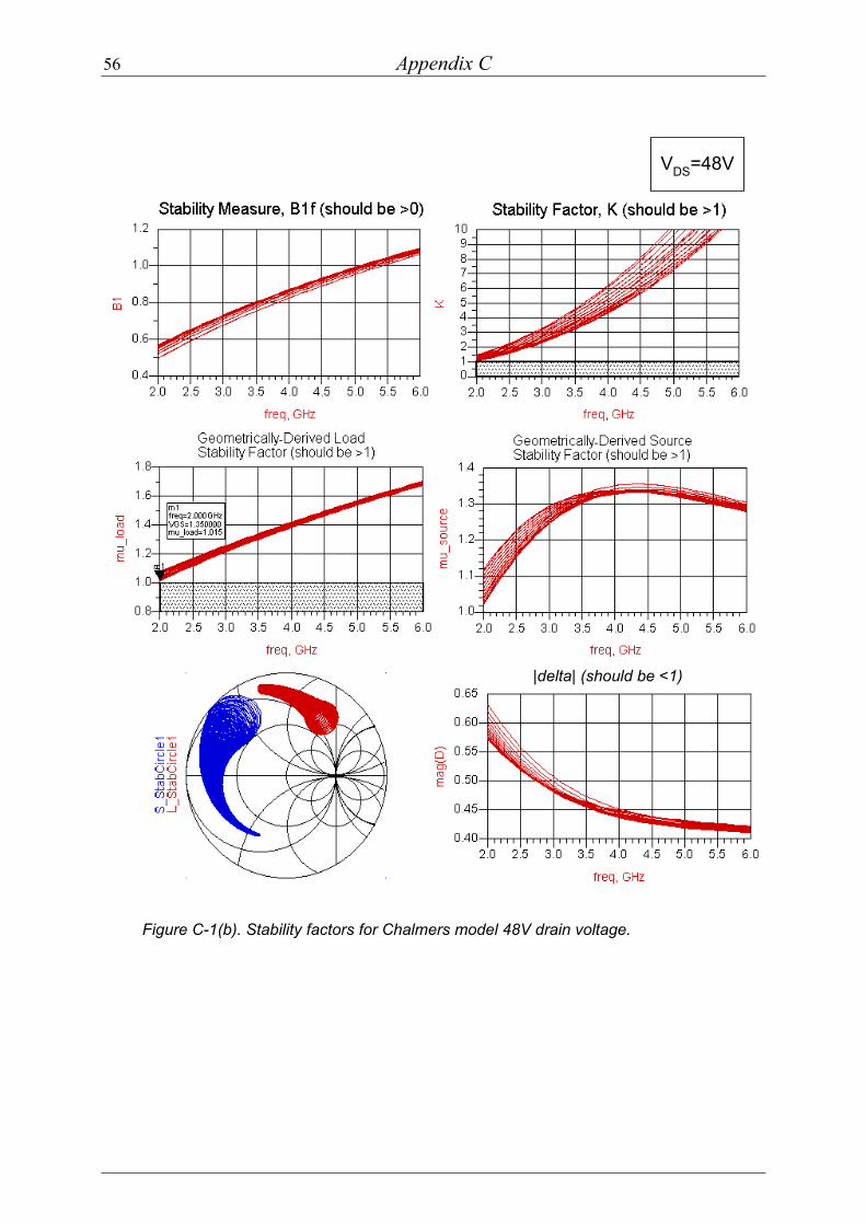
Appendix C. Stability simulation results C.1 Stability factors for Chalmers model for VDS=28, 48 V
It is considered VGS= [1.1-2.5] V for 2-6 GHz frequency range
Figure C-1(a). Stability factors for Chalmers’ model 28V drain voltage.
VDS=28V
|delta| (should be <1)
56 Appendix C
Figure C-1(b). Stability factors for Chalmers model 48V drain voltage.
VDS=48V
|delta| (should be <1)

Stability simulation results 57
C.1 Stability factors for Motorola’s model for VDS=28, 35 V.
It is considered: VGS= [3-5]V for 2-6 GHz frequency range.
Figure C-2. Stability factors for Motorola’s model 28 and 35 V drain voltage and VGS= [3 - 5]V.
|delta| (should be <1)
VDS=28, 35V

58 Appendix C

59
Appendix D. Maximum frequency oscillation (fmax) and Cut-off (fT) simulation data D.1 Maximum frequency oscillation (fmax) for Chalmers model
Figure D-1(b). Maximum available gain [dB] versus frequency [GHz]. The differentinput bias conditions are shown with drain voltage equal 48 V.
Frequency [GHz]
Figure D-1(a). Maximum available gain [dB] versus frequency [GHz]. The differentinput bias conditions are shown with drain voltage equal 28 V.
Frequency [GHz]
VDS=28V
VDS=48V
MAG
[dB]
MAG
[dB]

60 Appendix D
D.2 Maximum frequency oscillation (fmax) for Motorola’s model
Figure D-2(a). Maximum available gain [dB] versus frequency [GHz]. The differentinput bias conditions are shown with drain voltage equal 28 V.
Frequency [GHz]
Figure D-2(b). Maximum available gain [dB] versus frequency [GHz]. The differentinput bias conditions are shown with drain voltage equal 35 V.
VDS=28V
VDS=35V
MAG
[dB]
MAG
[dB]
Frequency [GHz]

Maximum frequency oscillation and cut-off simulation data 61
D.3 Cut-off frequency (fT) for Chalmers model (VDS=28,48V)
Figure D-3(a). Current gain [dB] versus frequency [GHz]. The differentinput bias conditions are shown with drain voltage equal 28 V.
Frequency [GHz]
Cur
rent
gai
n [d
B]
Figure D-3(b). Current gain [dB] versus frequency [GHz]. The differentinput bias conditions are shown with drain voltage equal 48 V.
Frequency [GHz]
Cur
rent
gai
n [d
B]
VDS=28V
VDS=48V

62 Appendix D
D.4 Cut-off frequency (fT) for Motorola’s model (VDS=28,35V)
Figure D-4(a). Current gain [dB] versus frequency [GHz]. The differentinput bias conditions are shown with drain voltage equal 35 V.
Frequency [GHz]
Cur
rent
gai
n [d
B]
Figure D-4(a). Current gain [dB] versus frequency [GHz]. The differentinput bias conditions are shown with drain voltage equal 28 V.
Frequency [GHz]
Cur
rent
gai
n [d
B]
VDS=28V
VDS=35V

Maximum frequency oscillation and cut-off simulation data 63
D.5 Maximum available gain versus frequency and VGS for Chalmers’ model
VDS=28VTable D-1(a). MAG versus frequency and VGS (VDS=28)

64 Appendix D
VDS=48VTable D-1(b). MAG versus frequency and VGS (VDS=48)

65
Appendix E. Small-signal simulation data E.1 Source/Load impedances for simultaneous matching
VDS=28V
VDS=48V
Table E-1(a). Source and Load impedances for simultaneousmatching approach (VDS=28)
Table E-1(b). Source and Load impedances for simultaneousmatching approach (VDS=48)

66 Appendix E
E.2 Small-signal gain optimization results
Figure E-1(a). Small-signal optimization results for 2.4 GHz (VDS=28, 48V).
Ferq=2.4GHz
Vds=28V, Vgs=1.165V
Vds=28V, Vgs=1.2V
Vds=28V, Vgs=1.5V
Vds=48V, Vgs=1.2V
Vds=48V, Vgs=1.5V
Vds=48V, Vgs=1.0V
VDS=28V

Small-signal simulation data 67
Figure E-1(b). Small-signal optimization results for 3.2 GHz (VDS=28, 48V).
Vds=28V, Vgs=1.165V
Vds=28V, Vgs=1.2V
Vds=28V, Vgs=1.5V
Vds=48V, Vgs=1.2V
Vds=48V, Vgs=1.5V
Vds=48V, Vgs=1.0V
Freq=3.2GHzVDS=28V VDS=48V

68 Appendix E
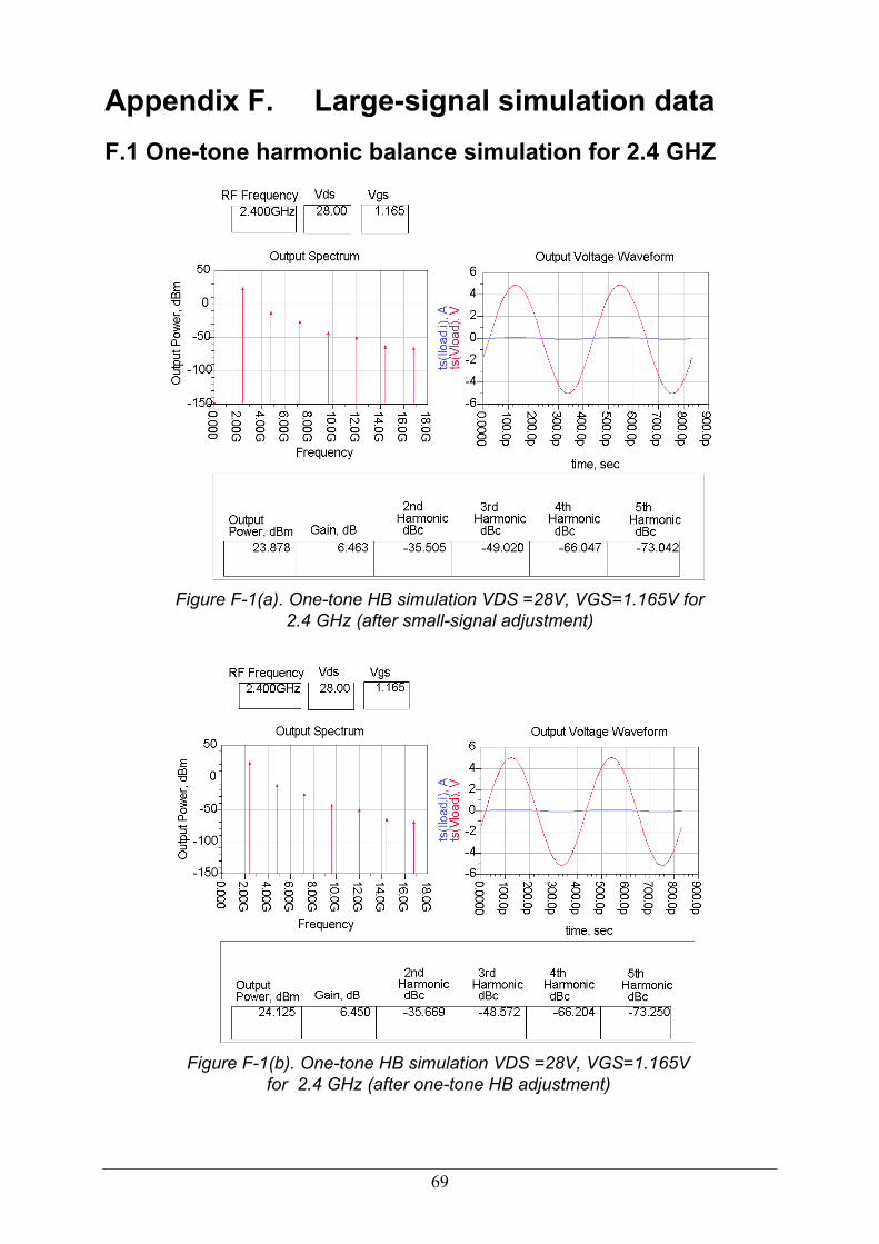
69
Appendix F. Large-signal simulation data F.1 One-tone harmonic balance simulation for 2.4 GHZ
Figure F-1(a). One-tone HB simulation VDS =28V, VGS=1.165V for2.4 GHz (after small-signal adjustment)
Figure F-1(b). One-tone HB simulation VDS =28V, VGS=1.165Vfor 2.4 GHz (after one-tone HB adjustment)

70 Appendix F
Figure F-1(c). One-tone HB simulation VDS =48V, VGS=1.0Vfor 2.4 GHz (after small-signal adjustment)
Figure F-1(d). One-tone HB simulation VDS =48V,VGS=1.0V for 2.4 GHz (after one-tone HB adjustment)

Large-signal simulation data 71
F.2 One-tone harmonic balance simulation for 3.2 GHz
Figure F-2(a). One-tone HB simulation VDS =28V, VGS=1.165V for3.2 GHz (after small-signal adjustment)
Figure F-2(b). One-tone HB simulation VDS =28V, VGS=1.165Vfor 3.2 GHz (after one-tone HB adjustment)

72 Appendix F
F.3 Two-tone harmonic balance simulation (2.4 GHz)
Figure F-3(a). Two-tone power sweep for 2.4 GHz(VDS=28,VGS=1.165V)
Input power [dBm] - 3
Figure F-3(b). Two-tone power sweep for 2.4 GHz(VDS=48,VGS=1.0V)
Input power [dBm] - 3

Large-signal simulation data 73
F.4 Two-tone harmonic balance simulation (3.2 GHz)
Figure F-3(c). Two-tone power sweep for 3.2 GHz(VDS=28,VGS=1.165V)
Input power [dBm] - 3
Figure F-3(d). Two-tone power sweep for 3.2 GHz (VDS=48,VGS=1.0V)Input power [dBm] - 3

74 Appendix F
F.5 Load-pull simulation
F.5.1 Deriving of optimum value for load impedance
F-4. Deriving of the optimum load impedance (3.2 GHz).

På svenska
Detta dokument hålls tillgängligt på Internet – eller dess framtida ersättare –under en längre tid från publiceringsdatum under förutsättning att inga extra-ordinära omständigheter uppstår.
Tillgång till dokumentet innebär tillstånd för var och en att läsa, ladda ner,skriva ut enstaka kopior för enskilt bruk och att använda det oförändrat för ick-ekommersiell forskning och för undervisning. Överföring av upphovsrätten viden senare tidpunkt kan inte upphäva detta tillstånd. All annan användning avdokumentet kräver upphovsmannens medgivande. För att garantera äktheten,säkerheten och tillgängligheten finns det lösningar av teknisk och administrativart.Upphovsmannens ideella rätt innefattar rätt att bli nämnd som upphovsman i denomfattning som god sed kräver vid användning av dokumentet på ovan beskrivnasätt samt skydd mot att dokumentet ändras eller presenteras i sådan form eller isådant sammanhang som är kränkande för upphovsmannens litterära eller konst-närliga anseende eller egenart.
För ytterligare information om Linköping University Electronic Press se för-lagets hemsidahttp://www.ep.liu.se/
In English
The publishers will keep this document online on the Internet - or its possiblereplacement - for a considerable time from the date of publication barring excep-tional circumstances.
The online availability of the document implies a permanent permission foranyone to read, to download, to print out single copies for your own use and touse it unchanged for any non-commercial research and educational purpose. Sub-sequent transfers of copyright cannot revoke this permission. All other uses ofthe document are conditional on the consent of the copyright owner. The pub-lisher has taken technical and administrative measures to assure authenticity,security and accessibility.
According to intellectual property law the author has the right to be men-tioned when his/her work is accessed as described above and to be protectedagainst infringement.
For additional information about the Linköping University Electronic Pressand its procedures for publication and for assurance of document integrity, pleaserefer to its WWW home page:http://www.ep.liu.se/
© Grigori Doudorov