Evaluation of Digital Power Control Algorithms for...
130
Chalmers University of Technology Department of Computer Science and Engineering Göteborg, Sweden, July 2011 Evaluation of Digital Power Control Algorithms for Automotive LED Headlights using TMS320F28035 Microcontroller Master of Science Thesis in Integrated Electronic System Design MUHAMMAD WAQAR AZHAR
Transcript of Evaluation of Digital Power Control Algorithms for...

Chalmers University of Technology Department of Computer Science and Engineering Göteborg, Sweden, July 2011
Evaluation of Digital Power Control Algorithms for Automotive LED Headlights using TMS320F28035 Microcontroller Master of Science Thesis in Integrated Electronic System Design
MUHAMMAD WAQAR AZHAR

Chalmers University of Technology Department of Computer Science and Engineering Göteborg, Sweden, July 2011
The Author grants to Chalmers University of Technology the non-exclusive right to publish the Work electronically and in a non-commercial purpose make it accessible on the Internet. The Author warrants that he/she is the author to the Work, and warrants that the Work does not contain text, pictures or other material that violates copyright law. The Author shall, when transferring the rights of the Work to a third party (for example a publisher or a company), acknowledge the third party about this agreement. If the Author has signed a copyright agreement with a third party regarding the Work, the Author warrants hereby that he/she has obtained any necessary permission from this third party to let Chalmers University of Technology store the Work electronically and make it accessible on the Internet. Evaluation of Digital Power Control Algorithms for Automotive LED Headlights using TMS320F28035 Microcontroller Muhammad Waqar Azhar © Muhammad Waqar Azhar, July 2011. Examiner: Prof. Per Larsson-Edefors Chalmers University of Technology Department of Computer Science and Engineering SE-412 96 Göteborg Sweden Telephone + 46 (0)31-772 1000

ACKNOWLEDGEMENTS
First of all. thanks to ALLAH Almighty for enabling me to complete this thesisand all the blessings upon me. Special thanks to Ole-Kristian Skroppa for
supervising my thesis and the support and motivation that he gave throughoutthis project. I would like to extend my gratitude towards my internal supervisor
Professor Per Larsson-Edefors and for his valuable feedback throughout mymaster degree. Moreover, I would like to thank the automotive application team,
especially Christoph Mendth, Matthias Terhorst, Roberto Scibilia and JosefMieslinger for their valuable help during different phases of project.
I would like to dedicate this work to my parents, my intelligent and hardworkingfather who has been an inspiration all through my life and my mother who’s love
and care has enabled me to reach this far in professional life. Last but not theleast i would like to thank rest of my family and friends for their extended support

Abstract
Digital power management solutions offer some distinct advantages over theiranalog counterparts and are increasingly being employed by power electronics de-signers these days. The post-implementation flexibility of digital solutions is oneof the major advantages. Increasing demands on functionalities like communica-tion, remote fault monitoring and configurability have also fueled this transitionfrom analog to digital control. The possibility of implementing non-linear con-trol algorithms is a major advantage of these solutions. Highly integrated analogcomponents, like analog to digital converters and comparators in modern micro-controllers, have enabled designers to decrease on-board component count andcomplexity. Digital power management solutions have limitations in performancewhen compared to analog designs, but rapid performance improvements in micro-controllers (MCUs) certainly create a bright future for digital power management.
In this project we have investigated a digital power control implementationfor switch mode DC-DC converters. The application under consideration is LED-based automotive headlights. LEDs (light emitting diodes) have gained footholdin many lighting applications due to the decrease in cost per lumen. The automo-tive industry has previously employed LEDs in a number of lighting application,like back and interior lighting, and now consider a potential use in headlights.Moreover we wanted to prove the capabilities of the TMS320F28035 MCU that isdesigned for real-time control applications. The combination of two new avenuesof digital power management and LED headlights has raised a few challenges thathave been solved in this project.
First, the characteristic behavior of LEDs is different from conventional in-candescent bulbs. LEDs are controlled by maintaining a constant current throughthem rather than applying a constant voltage. Switch mode power stages in-tended to control LEDs inherently operate in voltage mode. Considerable model-ing and implementation efforts are required to handle both these contrasting be-haviors. Secondly, discrete-time models are required for MCU implementation.Existing control theory predominantly employs continuous-time models. Thesecontinuous-time models are required to be converted to discrete-time models tomake use of existing models for digital implementation. Discrete-time modelsthat are developed from scratch requires considerable effort. Third, existing test-setups used for analog designs can not be directly used for digital designs. Con-siderable analysis is required for these modifications.

The first step in the design flow is modeling; we have to model convertersfor controlling current through LEDs. Two solutions are proposed: First, exist-ing continuous-time voltage mode models for converters are used and modifiedto control LEDs. Later some further modifications are made to convert them todiscrete time. Second, a new non-linear and discrete-time model is proposed forcontrolling LED current using inductor current feedback.
Later, the developed model is implemented on TMS320F28035. This MCUcontains two heterogeneous processor cores. A pre-implementation analysis iscarried out to allocate hardware resources and system bandwidth to different soft-ware tasks. The control loop is implemented on a so-called control-law accel-erator, as it is optimized for this purpose, while useful features like graphicaluser interface and diagnostics are implemented on C28x CPU. The initial band-width allocation to different software tasks is verified by doing measurementsand re-allocation. The initial implementation of different software components isalso optimized to enhance performance based on this post-implementation systemanalysis.
Lastly, the implemented control algorithms are verified by performing fre-quency response measurements. Modifications are made to existing test-setups tosuit them to needs of digital power control. Open loop and closed loop measure-ments are performed under different operating conditions. These measurementsare compared with results from the model and used to lay down our final analy-sis. Recursive design approach is used at each design phase. Moreover previousdesign phases are revisited whenever necessary to optimize the implementation.
Contents
1 Background and Theory 91.1 Problem Statement . . . . . . . . . . . . . . . . . . . . . . . . . 91.2 Project Work Flow . . . . . . . . . . . . . . . . . . . . . . . . . 101.3 What is LED . . . . . . . . . . . . . . . . . . . . . . . . . . . . 101.4 Application of LEDs in Automotive Lighting . . . . . . . . . . . 111.5 LEDs Characteristic Behavior . . . . . . . . . . . . . . . . . . . 131.6 Comparison Between Linear and Switch Mode Control . . . . . . 141.7 Switch Mode DC/DC Power Converter . . . . . . . . . . . . . . . 16
1.7.1 Buck Converter . . . . . . . . . . . . . . . . . . . . . . . 161.7.2 Boost Converter . . . . . . . . . . . . . . . . . . . . . . 161.7.3 SEPIC Converter . . . . . . . . . . . . . . . . . . . . . . 171.7.4 Comparison Between Different SMPS Topologies . . . . 18
1.8 Comparison Between Analog and Digital Power Management . . 191.8.1 Analog Controller . . . . . . . . . . . . . . . . . . . . . 201.8.2 Digital Power Management . . . . . . . . . . . . . . . . 201.8.3 Continuous vs Discrete Time Compensation . . . . . . . . 211.8.4 Comparison between Analog and Digital Power Management 21
2 Hardware Platform 232.1 Evaluation Module Overview . . . . . . . . . . . . . . . . . . . . 232.2 SMPS stages . . . . . . . . . . . . . . . . . . . . . . . . . . . . 24
2.2.1 Buck SMPS Stage . . . . . . . . . . . . . . . . . . . . . 242.2.2 Boost SMPS Stage . . . . . . . . . . . . . . . . . . . . . 242.2.3 Buck-Boost SMPS Stage . . . . . . . . . . . . . . . . . . 242.2.4 SEPIC SMPS Stage . . . . . . . . . . . . . . . . . . . . 25
2.3 Central Controller . . . . . . . . . . . . . . . . . . . . . . . . . . 262.3.1 TMS320F28035 Real-Time Micro-Controller . . . . . . . 262.3.2 Control Law Accelerator . . . . . . . . . . . . . . . . . . 282.3.3 Analog to Digital Converter . . . . . . . . . . . . . . . . 302.3.4 Enhanced Pulse Width Modulation Module . . . . . . . . 31
2.4 Pin Assignments . . . . . . . . . . . . . . . . . . . . . . . . . . 33
1

3 Design Considerations for LED Automotive Headlights 353.1 Design Matrices . . . . . . . . . . . . . . . . . . . . . . . . . . . 35
3.1.1 SMPS Modeling . . . . . . . . . . . . . . . . . . . . . . 353.1.2 Switching Frequency . . . . . . . . . . . . . . . . . . . . 363.1.3 Current Control vs Voltage Control . . . . . . . . . . . . 373.1.4 Life Cycle and Diagnostics . . . . . . . . . . . . . . . . . 37
4 Modeling and Compensation 384.1 Voltage-Mode Control . . . . . . . . . . . . . . . . . . . . . . . 38
4.1.1 Modeling of SMPS . . . . . . . . . . . . . . . . . . . . . 394.1.2 Compensation . . . . . . . . . . . . . . . . . . . . . . . 45
4.2 Current-Mode Control . . . . . . . . . . . . . . . . . . . . . . . 47
5 System Architecture and Firmware 525.1 Software Development Tools and Resources . . . . . . . . . . . . 52
5.1.1 Digital Power Library . . . . . . . . . . . . . . . . . . . 525.2 System Overview . . . . . . . . . . . . . . . . . . . . . . . . . . 525.3 Challenges Related to Discrete System Implementation . . . . . . 545.4 Hardware Initialization . . . . . . . . . . . . . . . . . . . . . . . 55
5.4.1 PWM Initialization . . . . . . . . . . . . . . . . . . . . . 565.4.2 ADC Initialization . . . . . . . . . . . . . . . . . . . . . 575.4.3 CLA Initialization . . . . . . . . . . . . . . . . . . . . . 58
5.5 Control Loop Implementation . . . . . . . . . . . . . . . . . . . 585.5.1 Control Loop Architecture . . . . . . . . . . . . . . . . . 595.5.2 System Architecture . . . . . . . . . . . . . . . . . . . . 605.5.3 Improvements in Control Loop Architecture . . . . . . . . 625.5.4 Control Loop Triggering . . . . . . . . . . . . . . . . . . 64
5.6 C28x Code . . . . . . . . . . . . . . . . . . . . . . . . . . . . . 655.7 PWM Dimming . . . . . . . . . . . . . . . . . . . . . . . . . . . 69
5.7.1 Limitation I . . . . . . . . . . . . . . . . . . . . . . . . . 705.7.2 Limitation II . . . . . . . . . . . . . . . . . . . . . . . . 71
5.8 Diagnostics . . . . . . . . . . . . . . . . . . . . . . . . . . . . . 735.8.1 Over-Voltage Protection . . . . . . . . . . . . . . . . . . 74
6 Measurement and Results 786.1 Measurement Equipment . . . . . . . . . . . . . . . . . . . . . . 786.2 Open-Loop Measurements . . . . . . . . . . . . . . . . . . . . . 79
6.2.1 Method I . . . . . . . . . . . . . . . . . . . . . . . . . . 806.2.2 Method II . . . . . . . . . . . . . . . . . . . . . . . . . . 806.2.3 Method III . . . . . . . . . . . . . . . . . . . . . . . . . 816.2.4 Digital Controller Measurement Setup . . . . . . . . . . . 81
2

6.2.5 Measurement Results . . . . . . . . . . . . . . . . . . . . 846.3 Closed-Loop Measurement . . . . . . . . . . . . . . . . . . . . . 866.4 Hardware Platform Improvement . . . . . . . . . . . . . . . . . . 90
7 Conclusion 92
A Matlab Models 98A.1 Buck . . . . . . . . . . . . . . . . . . . . . . . . . . . . . . . . . 98A.2 Boost . . . . . . . . . . . . . . . . . . . . . . . . . . . . . . . . 98A.3 Buck-Boost . . . . . . . . . . . . . . . . . . . . . . . . . . . . . 99A.4 SEPIC . . . . . . . . . . . . . . . . . . . . . . . . . . . . . . . . 100A.5 Filter Conversion Script . . . . . . . . . . . . . . . . . . . . . . . 100
A.5.1 Convert.m . . . . . . . . . . . . . . . . . . . . . . . . . . 100A.5.2 Convert2.m . . . . . . . . . . . . . . . . . . . . . . . . . 101
A.6 Current Mode Control . . . . . . . . . . . . . . . . . . . . . . . . 101
B Firmware 102B.1 Main.c . . . . . . . . . . . . . . . . . . . . . . . . . . . . . . . . 102B.2 2nd Order IIR Filter code . . . . . . . . . . . . . . . . . . . . . . 117B.3 3rd Order IIR Filter code . . . . . . . . . . . . . . . . . . . . . . 118B.4 CLA Code . . . . . . . . . . . . . . . . . . . . . . . . . . . . . . 119B.5 CLA ISR used for Dimming . . . . . . . . . . . . . . . . . . . . 121B.6 PWM Initialization . . . . . . . . . . . . . . . . . . . . . . . . . 122
C Source Code for Open Loop Measurement for Buck SMPS 124C.1 CLA Code . . . . . . . . . . . . . . . . . . . . . . . . . . . . . . 124C.2 Modifications in Main Code . . . . . . . . . . . . . . . . . . . . 125
3

List of Figures
1.1 Comparison of Luminous Efficiency based on Haitz Law . . . . . 111.2 Future trends in LED device efficiency . . . . . . . . . . . . . . . 131.3 Characteristic of an Ultra White Automotive LED [1] . . . . . . . 141.4 Linearly controlled LED setup [2] . . . . . . . . . . . . . . . . . 151.5 Generic buck architecture. . . . . . . . . . . . . . . . . . . . . . 171.6 Generic boost architecture. . . . . . . . . . . . . . . . . . . . . . 181.7 Generic SEPIC architecture. . . . . . . . . . . . . . . . . . . . . 191.8 Block diagram of SMPS controlled by analog controller . . . . . . 201.9 Block diagram of SMPS controlled by digital controller . . . . . . 21
2.1 General EVM board layout . . . . . . . . . . . . . . . . . . . . . 242.2 Detailed implementation of buck SMPS stage . . . . . . . . . . . 252.4 Detailed implementation of buck-boost SMPS stage . . . . . . . . 252.3 Detailed implementation of boost SMPS stage . . . . . . . . . . . 262.5 Detailed implementation of SEPIC SMPS stage . . . . . . . . . . 262.6 Functional block diagram of TM320F28035 [3] . . . . . . . . . . 27
4.1 Voltage control mode . . . . . . . . . . . . . . . . . . . . . . . . 394.2 Bode plot of Matlab model for buck converter . . . . . . . . . . . 424.3 Bode plot of Matlab model for boost converter . . . . . . . . . . . 444.4 Bode plot of Matlab model for buck-boost converter . . . . . . . . 454.5 Bode plot of Matlab model for SEPIC converter . . . . . . . . . . 464.6 Bode plot of compensated Matlab model for buck converter . . . . 474.7 Bode plot of compensated Matlab model for boost converter . . . 484.8 Two switching states of boost converter [4] . . . . . . . . . . . . 494.9 Bode plot for current mode control model for boost converter . . . 51
5.1 General software architecture. . . . . . . . . . . . . . . . . . . . 535.2 Sampling true average current . . . . . . . . . . . . . . . . . . . 545.3 Symmetric PWM waveform . . . . . . . . . . . . . . . . . . . . 565.4 Synchronization of PWM and triggering of ADC channels . . . . 575.5 CLA task control flow diagram . . . . . . . . . . . . . . . . . . . 58
4

5.6 3-pole 3-zero filter interfacing in control loop . . . . . . . . . . . 605.7 High resolution PWM driver . . . . . . . . . . . . . . . . . . . . 615.8 Control loop system implementation . . . . . . . . . . . . . . . . 625.9 Modified control loop system implementation . . . . . . . . . . . 635.10 Computation sequence of control loop . . . . . . . . . . . . . . . 645.11 Time line diagram of four control loops running on CLA . . . . . 655.12 C28x software architecture overview . . . . . . . . . . . . . . . . 665.13 State Machine A . . . . . . . . . . . . . . . . . . . . . . . . . . 665.14 State Machine B . . . . . . . . . . . . . . . . . . . . . . . . . . . 675.15 State Machine C . . . . . . . . . . . . . . . . . . . . . . . . . . . 685.16 Enable dimming task architecture . . . . . . . . . . . . . . . . . 695.17 Circuit Description of Dimming . . . . . . . . . . . . . . . . . . 705.18 Triggering of ISR handling dimming function . . . . . . . . . . . 715.19 Screen shot of dimming . . . . . . . . . . . . . . . . . . . . . . . 715.20 Screen shot of dimming after improvements . . . . . . . . . . . . 735.21 Over-voltage protection implementation I . . . . . . . . . . . . . 755.22 Over-voltage protection implementation II . . . . . . . . . . . . . 765.23 OVP screen shot for boost SMPS . . . . . . . . . . . . . . . . . . 77
6.1 Open-loop measurement circuit setup I [5] . . . . . . . . . . . . . 806.2 Open-loop measurement circuit setup II [5] . . . . . . . . . . . . 806.3 Open-loop measurement circuit setup III [5] . . . . . . . . . . . . 816.4 Open loop gain for buck converter . . . . . . . . . . . . . . . . . 816.5 Open-loop measurement setup . . . . . . . . . . . . . . . . . . . 836.6 Open-loop gain for buck converter . . . . . . . . . . . . . . . . . 846.7 Open-loop gain for boost converter . . . . . . . . . . . . . . . . . 856.8 Open-loop gain for SEPIC converter . . . . . . . . . . . . . . . . 856.9 Classical method for measuring frequency response [5] . . . . . . 866.10 Venable method for measuring frequency response [5] . . . . . . 876.11 Closed-loop measurement setup . . . . . . . . . . . . . . . . . . 886.12 Boost feedback loop measurement . . . . . . . . . . . . . . . . . 886.13 Buck feedback loop measurement setup . . . . . . . . . . . . . . 89
5

List of Tables
1.1 Comparison between conventional and LED light efficiency [6] . . 121.2 Comparison of analog and digital controller performance [7] . . . 22
2.1 Detailed list of peripherals in TMS320F28035 MCU [8] . . . . . 282.2 Pin connection on EVM . . . . . . . . . . . . . . . . . . . . . . . 33
6

List of Abbreviations
• ADC-Analog to Digital Converter
• CPU-Central Processing Unit
• DC-Direct Current
• ESR-Equivalent Series Resistance
• EVM-Evaluation Module
• GUI-Generic User Interface
• ISR-Interrupt Service Routine
• GPIO-General Purpose Input Output
• JTAG-Joint Task Action Group
• MCU-Micro Controller Unit
• FET-Field Effect Transistors
• OPAmp-Operational Amplifier
• PCB-Printed Circuit Board
• PWM-Pulse Width Modulation
• ePWM-Enhanced Pulse Width Modulation
• RISC-Reduced Instruction Set
• SMPS-Switch Mode Power Supplies
• TI-Texas Instruments
• USB-Universal Serial Bus
7

• DSP-Digital Signal Processor
• CLA-Control Law Accelerator
• HRPWM-High Resolution Pulse Width Modulation
• SYSCLKOUT-System Clock Signal
• RAM-Random Access Memory
• LED-Light Emitting Diode
• SAR-Successive approximation Register
• SOC-ADC channel control logic
• DPL-Digital Power Library
• IIR-Infinite Impulse Responce
• CCS-Code Composer Studio
• IDE-Integrated Development Environment
8

Chapter 1
Background and Theory
1.1 Problem StatementDigital control is being employed by commercial power supply designers. Thiscomprises both digital circuits and micro-controller (MCU) based solutions. Dig-ital circuit solutions give better performance and optimization because they aretailored to specifications, while MCU based solutions offer considerable perfor-mance with low cost and less time to market. Digital power control offers signifi-cant advantages over analog control.
The purpose of this project is to evaluate digital power control for switch modepower supplies (SMPS) driving LEDs. LED based automotive headlights is theunderlined product. This project deals with two combined problems. First, mod-eling of power LEDs and designing a control strategy for them using switch modepower supplies. Secondly, using digital power control for this implementation.The major design tasks are depicted below
• Efficient control algorithms for LEDs headlamps
• Optimal algorithm for pulse width modulation (PWM) dimming of LEDheadlamps
• Models for current mode control of switch mode power supplies
• Compensation based on above model
• MCU implementation and its trade-offs
• The relative importance of different diagnostic function has to be deter-mined to have an optimal implementation, as total system bandwidth is lim-ited
9

Modeling of SMPS in current mode needs considerable design space explo-ration because of lack of available published work. Different implementationstrategies are to be analyzed and solved, furthermore a post-implementation anal-ysis of system behavior and performance is also desirable to get a measure ofeffectiveness.
1.2 Project Work FlowFirst, SMPS driving power LEDs are modeled in MATLAB to evaluate systembehavior. Later on these models are used for MCU based implementation. Theimplementation consists of control law, communication and diagnostic functions.Texas Instrument’s TMS320F28035 real-time micro-controller is used for imple-mentation of digital power control algorithms. Later, performance of these im-plemented algorithms will be evaluated using a frequency response analyzer. Arecursive design approach between different design phases is employed to searchoptimal algorithms and implementation.
1.3 What is LEDLEDs differ from traditional light sources. In an incandescent lamp, a tungstenfilament is heated by electric current until it glows or emits light. In a fluorescentlamp, an electric arc excites mercury atoms, which emit ultraviolet (UV) radiation.After striking the phosphor coating on the inside of glass tubes, the UV radiationis converted and emitted as visible light. A LED, in contrast, is a semiconductordiode. It consists of a semiconductor p-n junction. When properly biased, currentflows from the p-side (anode) to the n-side (cathode) and light is emitted [9].However, silicon is unsuitable for making LEDs because the so-called energy bandgap is too low. The first LEDs were made from gallium arsenide (GaAs) andproduced infrared light at about 905 nm. The reason for producing this color isthe energy band gap, that is, the difference between the conduction band and thelowest energy level (valence band) in GaAs. When a voltage is applied across theLED, electrons are given enough energy to jump into the conduction band andcurrent flows. When an electron loses energy and falls back into the low energystate (the valence band), a photon (light) is often emitted [10].
LEDs provide several advantages over tradition light sources; as summarizedbelow
• Long life
• Robustness
10

• Small size
• Non-toxicity
• Versatility
• High energy efficiency
1.4 Application of LEDs in Automotive LightingWith advances in semiconductor technology, LEDs have started getting attentionfor usage as light sources. Recent advancements have considerably decreased thecost of Lumen per Watt to such a level that LEDs have started finding foothold ina lot of applications. Haitz law—a LED counterpart of Moore’s law for integratedcircuits—states that every decade, the cost per lumen falls by a factor of 10 andthe amount of light generated per LED package increases by a factor of 20, for agiven wavelength of light. A comparison between projected data based on Haitzlaw and real data for LED efficiency for past decade is shown in figure 1.1 [11].
lm
Figure 1.1: Comparison of Luminous Efficiency based on Haitz Law
11

The efficiency of LEDs has increased over the last decade. A lot of researchhas been done and power LEDs manufacturers are trying to keep up with the latestdevelopments. Before looking into the future trends in LEDs it is worthwhile toput down a comparison presented in table 1.4, conducted by United States Depart-ment of Energy [6].
CFL LEDLight SourceLamp lumen rating (lm) 860Light source wattage (W) 13 1LED manufacturer declared ”typical luminous flux” (lm/led) 100Number of lamps/LEDs per fixture 1 12Luminaire measurementsLuminaire lumens (lm) 514 589Measured luminaire wattage (W) 12 14Fixture efficiency 60Luminaire efficacy (lm/W) 42 42
Table 1.1: Comparison between conventional and LED light efficiency [6]
LEDs have gained a significant ground in recent years and are predicted tooutperform traditional light sources on the parameters of cost and efficiency. Astudy conducted by US Department of Energy (see figure 1.2) presents the pastdevelopment and future trends of commercial and laboratory based LED devices[12].
LEDs are experiencing an exponential growth, like integrated circuits densityhave experienced in last decade. LEDs are becoming increasingly efficient, mak-ing them likely and natural successors to conventional lighting solutions. Con-cerning automotive headlights, this replacement has started with some premiumcars having LED headlights. A continuous decrease in cost of Lumen per Wattwill certainly enable manufactures to use LED-based headlights in mid range carsin the coming years.
High efficiency is also a major factor. There has been a market shift towardenergy-efficient cars in recent years such as hybrid cars. LED-based lighting so-lutions, being more energy efficient, are more suitable for such cars. Accordingto a study, LED-based headlights can save 40% energy compared to halogen lamp[13]. LED-based headlights are more compact [14]. LEDs currently dominatethe tail and center-mounted brake light markets. The use of LED in headlampsis expected to reach 26% of the market by 2015, mainly replacing halogen lamps[15]. Moreover, LED-based lighting solutions have a significant safety advantage
12

1990 2000 2010 2020 2030
0
80
60
40
20
100
120
140
160
180
200
LED Market Device
DOE ProjectWorld Record for
Laboratory Devices
Projected LED Lab
Projected LED Market
Source:US Department of Energy
Eff
icie
ncy (
Lu
men
s p
er w
att
)
Figure 1.2: Future trends in LED device efficiency
over those using filament lamps. The time from current flow to light output in anLED is measured in nanoseconds. In a filament lamp the response time is about300 ms. This enables other drivers to quickly see critical signals, e.g., brakes [10].
1.5 LEDs Characteristic BehaviorA LED can be described as a constant voltage load. The voltage drop dependson the internal energy barrier required for the photons of light to be emitted andthis energy barrier defines color of light [10]. The I-V characteristic of a LED issimilar to a normal p-n junction diode. Below the turn-on threshold voltage, verylittle current will flow through it. Above threshold, current flow increases rapidlyfor incremental increases in forward voltage. The threshold for typical automo-tive, white LEDs is approximately 3.2 Volts [1]. The rise in forward current isexponential with respect to applied voltage above the threshold. Thus the LEDcan be modeled as a voltage source in series with a resistor. This is valid onlyat a single operating DC current, as the LED is non linear. If the DC operatingcurrent in the LED is changed, then the resistance of the model must be changedto reflect the new operating point. Additionally, at large forward currents, theLED operates at a high power level, which in turn begins to heat the die. As a re-sult, the LED’s forward voltage drop decreases and its dynamic impedance startsincreasing with respect to temperature. It is important to consider the thermalenvironment when the LED’s impedance is determined [16]. Moreover, lightingcharacteristics of LEDs, e.g., wavelength shift and luminance decay, are related
13

with its junction temperature. The thermal interaction of each LED will causechange in color [17]. The I-V characteristic curve of an automotive LED modulefrom OSRAM (LE UW D1W1 01) is shown in figure 1.3 [1]. The I-V curve isnon linear and current increases exponentially beyond the forward threshold volt-age. The slope of this curve at a specific operating DC current is a measure of thedynamic impedance.
13 14 15 16 17 18 19
F
0
200
400
600
800
1000
F
Figure 1.3: Characteristic of an Ultra White Automotive LED [1]
Power LEDs are used in automotive headlights. These headlights have slightlydifferent behavior than normal LEDs; these are current controlled devices com-pared to one used in interior and back lighting. The output luminous flux is de-termined by the forward current through them. That is why we need to controlcurrent through LEDs [18]. This fact need to be considered while modeling andimplementing the control algorithm.
1.6 Comparison Between Linear and Switch ModeControl
Two of the most common methods to drive LEDs are linear and switch mode con-verters. Linear converters are easier to control. A typical linearly controlled LEDis shown in figure 1.4, referenced from [2]. The control circuitry must monitorthe output voltage, and adjust the voltage driving gate to hold the output voltageat the desired value. In this case, a field effect transistor (FET) is operating in its
14

linear conduction mode, as compared to saturation mode in switch mode powersupplies (SMPS). Moreover, the FET is conducting continuously through oper-ation, while in SMPS the FET only conducts during its on-time, which in turndepends on the duty cycle. An increased conduction time of the FET in a linearregulator results in more losses. Consequently, low efficiency is one of the majordrawbacks. Moreover, in a linear converter, the load voltage should be alwayslower than the supply voltage. While the SMPS stage can drive a load with avoltage greater than supply voltage, driving LEDs from a SMPS stage can giveus better efficiency with less power dissipated in the FET. But control of SMPSdriver is more complex than linear driver [18].
VREF
Sense
Resistor
Control
+
–
Figure 1.4: Linearly controlled LED setup [2]
Considering the control of both techniques the linear control is very simple.The DC bias to the FET gate is controlled based on a feedback, to maintain con-stant current. In contrast, control for a SMPS stage is complex. The transferfunction of SMPS converters contain a number of poles and zeros. A feedbackcontrolled filter called compensator is designed to cancel out system poles toachieve the desired system gain in the required bandwidth region. The simplestof these compensator designs are far more complex than a linear mode controller.The choice between linear and switch mode power control is a trade off which isdriven by efficiency. That is why linear control is suitable for back and interiorlighting application, but not for headlights.
15

1.7 Switch Mode DC/DC Power ConverterAn investigation of the most common DC/DC power supply topologies is pre-sented in this section, with the perspective of digital power control. Topologiesused in our project are buck, boost and SEPIC; see details below.
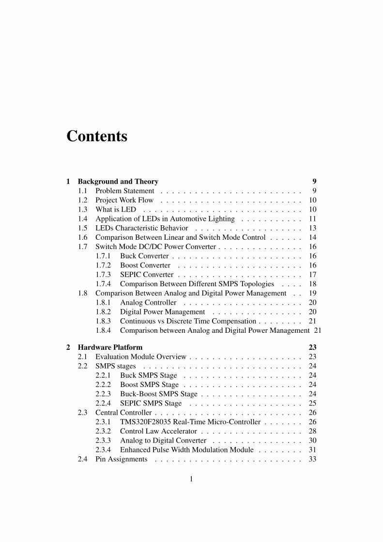
1.7.1 Buck ConverterThe buck converter is one of the most basic DC-DC switch mode converter. Itis a step down converter so its output voltage Vo ranges from the input voltageVi to 0. The output is not isolated from the input. The input current for a buckpower stage is discontinuous or pulsating, due to the power switch (Q1) currentthat pulses from zero to IO every switching cycle. The output current for a buckpower stage is continuous or non-pulsating, because the output current is suppliedby the output inductor-capacitor combination; the output capacitor never suppliesthe entire load current [19]. A generic implementation of a buck converter isshown in figure 1.5. Current and voltage waveforms are also presented in samefigure. The voltage conversion relationship in terms of duty cycle (D) is presentedin equation 1.1. The relationship between the output current and the inductorcurrent is presented in equation 1.2.
Vo = Vi ×D (1.1)
IL(avg) = IO (1.2)
1.7.2 Boost ConverterBoost is a non-isolated power stage topology, also called as step-up power stage.Power supply designers choose the boost power stage, because the required outputvoltage is always higher than the input voltage and has the same polarity. Theinput current for a boost power stage is continuous, because the input current isthe same as the inductor current. The output current for a boost power stage isdiscontinuous, because the output diode conducts only during a portion of theswitching cycle. The output capacitor supplies the entire load current for the restof the switching cycle [4]. A generic implementation of a boost converter is shownin figure 1.6, along with current and voltage waveforms.
16
Figure 1.5: Generic buck architecture.
Equation 1.3 shows the voltage translation between input and output voltage.The relationship between output and inductor current in terms of duty cycle (D)is shown in equation 1.4.
Vo =Vi
1−D(1.3)
IL(avg) =Io
1−D(1.4)
1.7.3 SEPIC ConverterSEPIC stands for single-ended primary-inductor converter. It can produce an out-put voltage Vo greater, less and equal to the input voltage Vi. A generic imple-mentation of a SEPIC converter is shown in figure 1.7. The SEPIC converteris similar to a buck-boost converter as both can step-up and step-down voltage.SEPIC has advantages such as isolation and non-inverting output, but has a farcomplex transfer function that needs higher-order compensator than buck, boostand buck-boost. A voltage translation equation in terms of duty cycle (D) is given
17

Inducter current Solid
Output Current Dashed
VQ Solid
Output Voltage Dashed
Figure 1.6: Generic boost architecture.
in 1.5.
Vo =Vi ×D
1−D(1.5)
1.7.4 Comparison Between Different SMPS TopologiesAll converter topologies discussed above are used for different applications de-pending upon input and output voltage ranges. Apart from this there are somestriking differences. Buck and boost converters are non-isolated, while the outputof SEPIC is isolated. Isolation can prevent short circuit current from input supply,in case of short circuit at output load. SEPIC is far more difficult to control thanbuck and boost as its frequency response contains more poles-zeros comparedto buck and boost. In addition to the inevitable fourth-order pole of SEPIC, an-other important feature in the transfer function is a single right half plane (RHP)zero. Right half plane zeros are a result of converters, where the response to anincreased duty cycle is to initially decrease the output voltage [20]. Isolation,voltage translation and compensator complexity are major trade-offs faced by theSMPS designer.
18

L1
Q L2
Cp
Cout
Q
IL1 SOLID
IIN DASHED
IL2 SOLID
IOUT DASHED
D* TS (1-D)* TS
TSVIN+VOUT
Figure 1.7: Generic SEPIC architecture.
1.8 Comparison Between Analog and Digital PowerManagement
Power management is an interdisciplinary area of modern electronics, merginghard-core analog circuit design with expertise from mechanical and RF engi-neering, safety and EMI, materials, semiconductors and magnetic components.Traditionally power supply design is considered an analog trade. But from thevery early days, by the introduction of relays and rectifiers, power managementis slowly incorporating more and more ideas from the digital world. The intro-duction of switched mode power conversion required even more digital circuits.Integrated pulse width modulators have introduced even more digital content topower management. Today’s highly integrated power management ICs are packedwith digital modules, e.g., pulse width modulators and timers. The digital circuitsallow the integration of some highly sophisticated features like EEPROM basedtrimming after packaging to eliminate package stress related initial offsets, digitaldelay techniques to adjust proper timing of gate drive signals, micro-controllersand state machines for battery charging and management [7].
19

1.8.1 Analog ControllerAnalog control design is traditionally used for switch mode DC-DC converters.A typical block diagram of an analog controller is shown in figure 1.8. It is im-portant to mention that analog compensation blocks in analog controller consistof hardwired circuits and components. This implementation is inflexible and notconfigurable. That is a major drawback of analog compensation. However, highbandwidth and low response time to input changes are some of benefits in usinganalog controllers over alternative designs options.
ref
Figure 1.8: Block diagram of SMPS controlled by analog controller
1.8.2 Digital Power ManagementDigital power management is a new direction in power supply controller design,to replace the analog circuits by digital implementations. Digital power stands fordigital control of the power supply. Digital power supply control attempts to movethe barrier between the analog and digital sections of the power supply right to thepins of the control IC [7]. Increased complexity and performance requirementsin the discrete analog design of power electronics control have led designers toincreasingly consider digital control solutions.
First let us review a digital control model as depicted in figure 1.9. Two ma-jor differences from an analog controller are the analog-digital converter (ADC)and the compensator. The analog compensator is here replaced by a digital one,which is either a software implementation executing on a MCU or a hardwaresolution implemented on an FPGA. Flexibility is a noteworthy advantage of thisdigital implementation, offering, first, adjustability. That is, every parameter—including voltage and current thresholds, operating frequency, thermal shut down,and startup time—which is measured or programmed can also be adjusted by thedigital controller on the fly. Second, flexibility can be used to invoke differentcontrol algorithms as the operating conditions of the power supply are changing.
20

Lastly, due to highly integrated communication peripherals in modern MCUs, theflexibility of the digital approach is greatly enhanced through the on-the fly pro-grammability [7].
Feedback
Amplifier
Figure 1.9: Block diagram of SMPS controlled by digital controller
It’s important to note that deployment of digital control had no effect on theoperating principle and the design of the power stage. The specification of thepower supply still determines the choice of topology, the selection of power com-ponents and the required control functions. That leaves a fair amount of designtasks still in the analog realm for the power supply experts [7].
1.8.3 Continuous vs Discrete Time CompensationAnalog compensation employs continuous-time S-transforms, while digital com-pensation employs discrete z-transforms. On the theoretical front, the majority ofpresent implementations translate S-domain transfer functions to Z-domain. Thisapproach permits utilization of the well understood linearized small signal modelsof switch mode converters. Once the poles and zeros are calculated to ensure thestability of the system, the Z coefficients of the digital transfer function can befound easily. The weakness of this method is that by starting from a linearizedmodel, the benefits of a higher-performance non-linear control theory can not befully utilized. As a result, the performance of power supplies using either digitalor analog controllers are very similar today [7].
1.8.4 Comparison between Analog and Digital Power Manage-ment
The striking difference between analog and digital control is the quality and theamount of information available for the controller to make decisions regarding theoperation of the power stage. The schemes have their respective advantages anddisadvantages. Analog controllers have very high bandwidth and low response
21

times, while digital controllers are weaker on these parameters in exchange forflexibility and configurability; features that are absent from analog controllers.Table 1.8.4 is formulated to present a comparison between the techniques [7].
Control Properties Analog DigitalSwitching frequency (CPU limitations) + -
Precision(tolerances,aging,temperature effects,drift,offset, etc.) - +
Resolution (numerical problems, quantization, rounding, etc.) + -
Bandwidth (sampling loop, ADC . DAC speed) + -
Instantaneous over current protection + -
Compatibility with power components + -
Power requirements + -
Communication, data management - +
Understanding theory + -
Advanced control algorithm (non-linear control, improved transient) - +
Multiple loops - +
Cost of controller + -
Cost of a platform (flexibility, time to market) - +
Component count(comparable functionality, integration) - +
Reliability + ?
Table 1.2: Comparison of analog and digital controller performance [7]
22

Chapter 2
Hardware Platform
2.1 Evaluation Module OverviewA LED demo evaluation module (EVM) was available to demonstrate a workingdemo of LED-based automotive headlights based on the concept of digital powermanagement using a micro-controller. We used the C2000 family MCU fromTexas Instruments. The C2000 series is based on a 32-bit CPU, called C2000 orC28x, with different variations of analog and digital peripherals [21]. An impor-tant feature is that the EVM is based on the dual inline socket (DIMM), so any ofthe C2000 series control sticks can be plugged in. We preferred the latest micro-controller available in the Piccolo B family, i.e., TMS320F28035. Developmentof this EVM was not part of this project but it’s worthwhile to mention all thenecessary details for the readers to comprehend the firmware development in laterpart of this report. Broadly an EVM can be divided into two main sections
• SMPS stages
• Central controller
There are four different SMPS stages on our EVM because of two reasons:First, this EVM has been built to support different ranges of LEDs. Differentranges of LEDs require different voltage ranges which in turn are provided bydifferent SMPS converters. Secondly, the purpose of this project is to evaluateand compare between different SMPS topologies with the perspective of digitalpower control. Certainly in a standard product one has to choose between theseconverters as some of them as easy to use along with their pros and cons. Figure2.1 shows a high-level layout of the EVM.
23

Figure 2.1: General EVM board layout
2.2 SMPS stagesThe detailed implementation of different converters is described in subsequentsections. One important fact that applies to all of converters is that there arecurrent feedbacks available from two different points on this EVM; first from theoutput current and second from the inductor current. These two feedbacks give usthe option to design a compensator based on any of these feedbacks.
2.2.1 Buck SMPS StageThe detailed implementation of a buck SMPS stage is shown in figure 2.2. Thisis a standard buck implementation as explained in section 1.7.1. Please note thatthe internal inductor resistance is used as a current shunt for the inductor currentfeedback.
2.2.2 Boost SMPS StageThe detailed implementation of a boost SMPS stage is shown in figure 2.3. Thisis a standard boost implementation as explained earlier in section 1.7.2.
2.2.3 Buck-Boost SMPS StageThe detailed implementation of buck-boost SMPS stage implementation is shownin figure 2.4. It is important to mention that this is not a standard buck-boost im-plementation, but actually it is a boost converter whose output load is connected
24

OP-AMP
Gate
Driver
PWM from Microcontroller
Rshunt
Inducter
Current
Feedback
Output
Current
Feedback
out
in Cin
RL
OP
-AM
P
Figure 2.2: Detailed implementation of buck SMPS stage
between the converter’s output and input node. Apart from the output load con-nection, this circuit is the same as the boost converter described in section 2.2.2.
RshuntOP-AMP
in
out
InducterCurrent
Feedback
Gate
Driver
PWM from
Microcontroller
Rshunt
Output
Current
Feedback
in
OP-AMP
Figure 2.4: Detailed implementation of buck-boost SMPS stage
2.2.4 SEPIC SMPS StageThe detailed implementation of a SEPIC SMPS stage implementation is shownin figure 2.5. This is a standard SEPIC implementation as explained earlier insection 1.7.3.
25

Rshunt OP-AMP
RshuntOP-AMP
in
out
Inducter
Current
Feedback
Output
CurrentFeedback
GateDriver
PWM from
Microcontroller
Cin
Figure 2.3: Detailed implementation of boost SMPS stage
Rshunt
+
_OP-AMP
in
out
Inducter
Current
Feedback
OutputCurrent
Feedback
Gate
Driver
PWM from
Microcontroller
Rshunt
+
_OP-AMP
L2
L1
Cin
C1
C2
Q
D1
+
_
Figure 2.5: Detailed implementation of SEPIC SMPS stage
2.3 Central ControllerThe TMS320F28035 micro-controller from the C2000 family is serving as centralcontrol unit on the EVM.
2.3.1 TMS320F28035 Real-Time Micro-ControllerThe TMS320F2803x family of micro-controllers combines the power of the C2000processor core and the control law accelerator (CLA) along with highly integratedperipherals. C2000 is a 32-bit processor developed by Texas Instruments. CLAis a 32-bit floating point coprocessor designed to implement control-centric algo-rithms with details available in section 2.3.2. This MCU is code-compatible with
26

previous C2000-based controllers. An internal voltage regulator allows for sin-gle rail operation. Analog comparators with internal 10-bit references have beenadded and can be used directly to control the PWM outputs. It also contains apowerful ADC that supports 0 to 3.3 V fixed full scale range conversion and alsoa ratio-metric conversion based on VREFHI/VREFLO references. The ADC inter-face has been optimized for low access overhead. A high resolution pulse widthmodulation (HRPWM) module is available to enable a more precise control[3].To give a perspective, the block diagram is presented in figure 2.6.
3 External Interrupts
M0
SARAM 1Kx16
(0-wait)
16-bit Peripheral Bus
SP
IST
Ex
M1
SARAM 1Kx16
(0-wait)
eCAN
(32-mailbox)
SCI
(4L FIFO)
ePWMSPI
(4L FIFO)
I2C
(4L FIFO)LIN
HRPWM
eCAP
32-Bit Peripheral Bus
GPIO MUX
C28x32-bit CPU
A7:0
B7:0
PIE
CPU Timer 0
CPU Timer 1
CPU Timer 2
TCK
TDITMS
TDO
TRST
OSC1,
OSC2,
Ext,
PLL,
LPM,
WD
XCLKIN
X2
XRS
32-bit Peripheral Bus(CLA accessible)
EC
AP
x
EP
WM
xA
EP
WM
xB
ES
YN
CI
ES
YN
CO
CA
NT
Xx
CA
NR
Xx
SD
Ax
SC
Lx
SP
ISIM
Ox
SP
ISO
MIx
SP
ICL
Kx
COMP1OUT
SC
IRX
Dx
GPIOMux
LPM Wakeup
CLA
ADC
PSWD
FLASH
32K/64K x 16
Secure
OTP/Flash
Wrapper
Boot-ROM
8Kx16
(0-wait)
SARAM
8K x 16
(0-wait)
Secure
LIN
AR
X
LIN
AT
X
COMP
32
-bi t
pe
r ip
he
ral
bu
s
(CL
Aa
cce
ss
ible
)
COMP1A
COMP1BCOMP2A
COMP2BCOMP3A
COMP3B
COMP2OUT
COMP3OUT
eQEP
EQ
EP
xA
EQ
EP
xB
EQ
EP
xI
EQ
EP
xS
SC
ITX
Dx
X1
GPIO
MUX
AIO
MUX
VREG
OTP 1K x 16Secure
(CLA Only on 6K)
FromCOMP1OUT,COMP2OUT,COMP3OUT
POR/BOR
Mem
ory
Bu
s
CL
AB
us
Memory Bus
Memory Bus
TZ
x
CodeSecurityModule
Figure 2.6: Functional block diagram of TM320F28035 [3]
To give a further insight of the integrated peripherals in TMS320F28035, atable 2.3.1 of peripherals is given.
27

TMS320F28035CPU 1 C28xPeak MMACS 60Frequency (MHz) 60CLA 1RAM (kB) 20OTP ROM (kB) 2Flash (kB) 128PWM 14CAP/QEP 1/1ADC 1 12bitADC Channels 14CLA 1ADC Conversion Time (nsec) 217I2C 1UART 1 SCISPI 2CAN 1Timers 3 32bit GP,Watchdog Timers 1GPIO 45Core Supply (V) 1.8I/O Supply (V) 3.3
Table 2.1: Detailed list of peripherals in TMS320F28035 MCU [8]
2.3.2 Control Law AcceleratorThe CLA is an independent and fully-programmable 32-bit floating-point mathprocessor. As name implies, it brings concurrent control-loop execution capabil-ity. It’s low interrupt latency allows it to read ADC samples just-in-time. Thisreduces the ADC sample to output delay to enable faster system response andfaster control loops. By using the CLA to service time-critical control loops, themain CPU is free to perform other system tasks such as communications and di-agnostics [22].
Functional Overview
The control law accelerator extends the capabilities of the C2000 CPU by addingparallel processing. The CLA is clocked at the same rate as the main CPU. It has
28

an independent bus architecture consisting of separate data and program buses. Itcontains an independent eight-stage pipeline. The register file contains four 32-bitresult registers (MR0-MR3), two 16-bit auxiliary registers (MAR0, MAR1) and aspecial function status register (MSTF). Communication between main CPU andCLA is done through two dedicated message RAMs for simplex communicationbetween the CLA and the main CPU. The CLA has direct access to the ePWM2.3.4, the HRPWM 2.3.4, the comparator and the ADC result registers. This factmakes it very suitable for implementation of control algorithms, also called con-trol laws. Because the control algorithm accesses ADC and PWM registers inevery loop iteration, providing access of these registers directly to CLA withoutany help from main CPU has significantly decreased the access latency. The over-all effect would be a faster control loop. The main CPU can map CLA programand data memory to the main CPU space or CLA space.
CLA Instruction Set
The CLA instruction set supports IEEE single-precision (32-bit) floating pointmath operations. Moreover, some parallel instructions are provided for code opti-mization. A list below shows all the instructions.
• Floating-point math with parallel load or store
• Floating-point multiply with parallel add or subtract
• 1/X and 1/sqrt(X) estimations
• Data type conversions
• Conditional branch and call
• Data load/store operations
CLA Programming
As the CLA can function independent of the main CPU it executes its own pro-gram. The program code for the CLA is written in assembly as there is no com-piler available yet. This code is compiled into a separate section using compilerdirective. This section is placed in a specific memory bank reserved for the CLAprogram. The CLA program code can consist of up to eight tasks or interrupt ser-vice routines. The start address of each task is specified by the MVECT registers.There is no limit on task size as long as the tasks fit within the CLA programmemory space. One task is serviced at a time through to completion. There is nonesting of tasks. Upon task completion a task-specific interrupt is flagged within
29

the PIE. When a task finishes the next highest-priority pending task is automati-cally started. Each task can be triggered by following method.
• From C28x CPU via the IACK instruction
• Task1 to Task7 can be triggered by the corresponding ADC or ePWM mod-ule interrupts
• Task8 can be triggered by ADCINT8 or by CPU Timer 0
2.3.3 Analog to Digital ConverterThe 12-bit ADC module in TMS32028035 is partly based on successive approx-imation registers (SAR) and partly pipelined. SAR uses a binary search throughall possible quantization levels before finally converging upon a digital output foreach conversion. A pipeline ADC uses two or more steps of sub-ranging. First,a coarse conversion is done. In a second step, the difference to the input signalis determined with a digital to analog converter (DAC). This difference is thenconverted finer, and the results are combined in a last step. The exact internalarchitecture of the ADC is not available due to commercial secrecy.
The ADC runs at full system clock and no pre-scaling is required. The coreof the ADC contains a single 12-bit converter which is fed by two sample andhold circuits, which in turn are fed by a total of up to 16 analog input channels.The sample and hold circuits can be sampled simultaneously or sequentially. Theconverter can be configured to run with an internal band gap reference (0 - 3.3V) to create true voltage based conversions. It can also use external voltage refer-ences VREFHI/VREFLO to create ratio-metric based conversions. This ADC is notsequencer based, however, it is easy for the user to create a series of conversionsfrom a single trigger using software. The basic principle of operation is centeredaround the configurations of individual conversions called SOC (start of conver-sion). These SOCs can be configured for trigger, sample window and channel.The ADC can be triggered by multiple sources as listed below [23].
• S/W - software immediate start
• ePWM 1-7
• GPIO XINT2
• CPU Timers 0/1/2
• ADCINT1/2
30

2.3.4 Enhanced Pulse Width Modulation ModuleThe enhanced pulse width modulator (ePWM) peripheral is a key element in con-trolling many of the power electronic systems found in both commercial and in-dustrial equipments. These systems include digital motor control, switch modepower supply control, un-interruptible power supplies (UPS). The ePWM periph-eral performs a DAC function, where the duty cycle is equivalent to a DAC analogvalue. An effective PWM peripheral must be able to generate complex pulse widthwaveforms with minimal CPU overhead or intervention. It needs to be highly pro-grammable and very flexible while being easy to understand and use. The ePWMunit described here addresses these requirements by allocating all needed timingand control resources on a per ePWM channel basis. Cross coupling or sharingof resources has been avoided, instead each ePWM is built up from smaller sin-gle channel modules with separate resources that can operate together as requiredto form a system. This modular approach results in an orthogonal architectureand provides a more transparent view of the peripheral structure, helping users tounderstand its operation quickly [24].
Functional Overview
The ePWM module represents one complete PWM channel composed of twoPWM outputs, EPWMxA and EPWMxB. Seven ePWM modules are present inthis device. Each ePWM instance is identical with one exception. Some instancesinclude a hardware extension that allows more precise control of the PWM out-puts. This extension is the high-resolution pulse width modulator (HRPWM). TheePWM modules are chained together via a clock synchronization scheme that al-lows them to operate as a single system when required. Additionally, this syn-chronization scheme can be extended to the capture peripheral modules (eCAP).Modules can also operate stand-alone. Each ePWM module supports the follow-ing features [24]:
• Dedicated 16-bit time-base counter with period and frequency control
• Two PWM outputs (EPWMxA and EPWMxB) that can be used in the fol-lowing configurations:
– Two independent PWM outputs with single-edge operation
– Two independent PWM outputs with dual-edge symmetric operation
– One independent PWM output with dual-edge asymmetric operation
• Asynchronous override control of PWM signals through software
31

• Programmable phase-control support for lag or lead operation relative toother ePWM modules
• Hardware-locked (synchronized) phase relationship on a cycle-by-cycle ba-sis
• Dead-band generation with independent rising and falling edge delay con-trol
• Programmable trip zone allocation of both cycle-by-cycle trip and one-shottrip on fault conditions
• A trip condition can force either high, low, or high-impedance state logiclevels at PWM outputs
• All events can trigger both CPU interrupts and ADC start of conversion(SOC)
• Programmable event pre-scaling minimizes CPU overhead on interrupts
• PWM chopping by high-frequency carrier signal, useful for pulse trans-former gate drives
High Resolution PWM Module
The HRPWM module extends the time resolution capabilities of the convention-ally derived PWM. HRPWM is typically used when PWM resolution falls below9-10 bits. This module supports both duty cycle and phase-shift control methods.The high resolution capability is only implemented on the A signal path of PWM,that is, on the EPWMxA output. The EPWMxB output has the conventional PWMcapability [25].
32
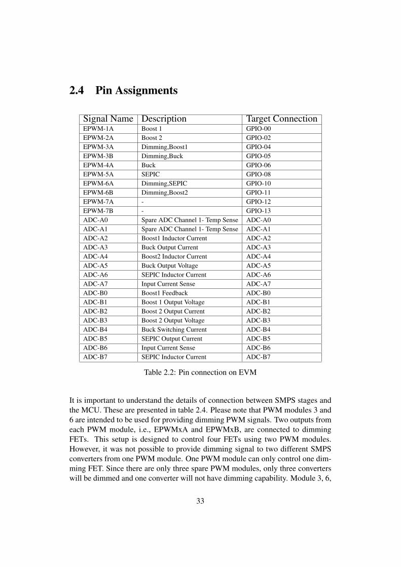
2.4 Pin Assignments
Signal Name Description Target ConnectionEPWM-1A Boost 1 GPIO-00EPWM-2A Boost 2 GPIO-02EPWM-3A Dimming,Boost1 GPIO-04EPWM-3B Dimming,Buck GPIO-05EPWM-4A Buck GPIO-06EPWM-5A SEPIC GPIO-08EPWM-6A Dimming,SEPIC GPIO-10EPWM-6B Dimming,Boost2 GPIO-11EPWM-7A - GPIO-12EPWM-7B - GPIO-13ADC-A0 Spare ADC Channel 1- Temp Sense ADC-A0ADC-A1 Spare ADC Channel 1- Temp Sense ADC-A1ADC-A2 Boost1 Inductor Current ADC-A2ADC-A3 Buck Output Current ADC-A3ADC-A4 Boost2 Inductor Current ADC-A4ADC-A5 Buck Output Voltage ADC-A5ADC-A6 SEPIC Inductor Current ADC-A6ADC-A7 Input Current Sense ADC-A7ADC-B0 Boost1 Feedback ADC-B0ADC-B1 Boost 1 Output Voltage ADC-B1ADC-B2 Boost 2 Output Current ADC-B2ADC-B3 Boost 2 Output Voltage ADC-B3ADC-B4 Buck Switching Current ADC-B4ADC-B5 SEPIC Output Current ADC-B5ADC-B6 Input Current Sense ADC-B6ADC-B7 SEPIC Inductor Current ADC-B7
Table 2.2: Pin connection on EVM
It is important to understand the details of connection between SMPS stages andthe MCU. These are presented in table 2.4. Please note that PWM modules 3 and6 are intended to be used for providing dimming PWM signals. Two outputs fromeach PWM module, i.e., EPWMxA and EPWMxB, are connected to dimmingFETs. This setup is designed to control four FETs using two PWM modules.However, it was not possible to provide dimming signal to two different SMPSconverters from one PWM module. One PWM module can only control one dim-ming FET. Since there are only three spare PWM modules, only three converterswill be dimmed and one converter will not have dimming capability. Module 3, 6,
33

7 will be used for dimming boost-1, SEPIC, boost-2 respectively. The buck con-verter is not dimmed. Since there is no connection between module 7 and boost-2SMPS, a jumper is placed to enable this modification.
34
Chapter 3
Design Considerations for LEDAutomotive Headlights
LEDs are largely used in automotive applications, e.g., in back lighting, interiorlighting and panel lighting. Use of LEDs in headlamps was only limited to a fewpremium cars until recent breakthroughs in technology. LEDs offer a number ofadvantages, such as far better energy efficiency, over conventional incandescentbulbs which are traditionally used in automotive headlights. This makes themsuitable for battery operated systems. A number of design matrices are identifiedfor a digital power controller for automotive LED headlights. This will simplifythe design process.
3.1 Design MatricesIdentification of design trade offs early in the design process could help simplifydesign effort. Some of these are based on theoretical aspects related to modelingand compensation. Moreover, some are related to the MCU-based implementationand the switching frequency. Each of these design trade offs are presented insubsequent sections.
3.1.1 SMPS ModelingEfficient system modeling is always required for effective control. Control algo-rithms are built around these models for precise and effective control. Accuratesystem models are normally more detailed and consequently controls are morecomplex. The efficiency of a model is directly proportional to its complexity. Inpractice, some details are left out due to limitations of implementation technology.This also applies to switch mode converters. The converter model complexity di-
35

rectly translates into higher filter order in the compensator. In an MCU-based im-plementation this means more instructions in compensator software, that is, longercomputation time, that in turn defines the upper limit of switching frequency. Fur-thermore, a general model is more complex than one tailored to specific operatingconditions.
SMPS are inherently non-linear due to the presence of switching devices likeFETs and diodes. Averaging approximations can be used to develop linear modelsof these components [26],[27]. This modeling approach tends to lose importantinformation on system behavior due to averaging approximation. Controller im-plementations based on this model are thus less efficient. MCU-based implemen-tations give choice of implementing complex and non-linear models. Consideringthe digital control implementation, its full capability is not used while using linearmodels. Instead, non-linear models are required to fully exploit the capabilities ofan MCU-based digital controller. Modeling SMPS efficiently for specific designspecifications and implementation technology could help reducing complexity ofplant and consequently the complexity of compensator.
3.1.2 Switching FrequencyThe switching frequency in SMPS is one of the most important parameters. SMPSare inherently non-linear due to PWM switching. Small signal stability is ensuredby averaging approximations used to model these SMPS in the linear domain.Theoretically such approximations are only valid for half of the switching fre-quency as proposed by the Nyquist criterion, but in practice the model is far morelimited, to 1/10 to 1/7 of the switching frequency. Consequently the compensa-tion designed to control these SMPS is also valid in similar limits. So a systemwith higher switching frequency can compensate high frequency perturbations.That means that an increased sampling frequency can increase the stability of thesystem [28]. Furthermore, a higher frequency in SMPS means less output ripple,because higher frequency components are easier to filter out by using low passfilters in the power stage.
In case of digital power management, practical limits are introduced due toMCU-based implementation: The master clock frequency and the sampling timesof the ADC are the major limiting factors. The software complexity of the con-trol loop, determined by the underlying SMPS topology, also imposes a limit.For example, the transfer function of a SEPIC converter is more complex than abuck converter, as it contain a fourth-order pole and a right half plane zero. Con-sequently, a software implementation of the control law for SEPIC will containmore instructions than that for buck, and the control loop for SEPIC will thustake more clock cycles than that for buck. Assuming the same system clock, therepetition frequency of the control loop for SEPIC will be less than that of buck.
36

Moreover, the switching frequency will determine the bandwidth availability toother software tasks. All these factors make switching frequency an importantparameter in design trade offs.
3.1.3 Current Control vs Voltage ControlLED-based automotive headlights behave quite differently than their incandescentcounterparts. Traditionally the luminance of incandescent bulbs are controlled bycompensating the voltage applied to them. In contrast, LEDs are controlled bycompensating the current through them. Voltage-mode control implies that theoutput voltage to a LED string is controlled and the resulting current, measuredby a shunt, is used as a feedback parameter to control the output voltage usingPWM duty cycle. This technique is indeed an indirect way to control the current.Current-mode control, also referred as current injection control, uses the fact thatthe average inductor current has a proportional relationship with average outputcurrent. So controlling the average current in an inductor can control the aver-age output current. This is a more direct approach based on current injection intosystem. Modeling the system in current mode can reduce the system order, conse-quently reducing the order of the compensator. A lack of documentation availableon current mode control in the context of digital power management is a majorhurdle in our case. In contrast, voltage-mode control is well known and a lot ofpublished work is available. These two modeling alternative serve as an importanttrade off; note that the different complexity of the respective compensator has aneffect on switching frequency too.
3.1.4 Life Cycle and DiagnosticsAutomotive based designs are always constrained by life cycle considerations. Byusing necessary diagnostic functions, expensive pieces of equipment can be safe-guarded from damage. Considering a digital controller, it’s easy to implementdiagnostics; additional logic is required in the case of analog controllers. In digitalpower management, control loops and diagnostic functions can share the sameMCU using time-sharing techniques. But diagnostics need a fair share from thevaluable system bandwidth. System bandwidth is first allocated to the controlalgorithm to fulfill specifications. The rest of the bandwidth is shared betweendiagnostics, communication and system monitoring. A comprehensive analysis ofrelative importance and time-to-action margins for different diagnostic functionsis required to estimate bandwidth requirements of different diagnostic functions.
37

Chapter 4
Modeling and Compensation
Modeling of SMPS converters is the first of the tasks at hand. There are twocurrent feedback alternatives available in each converter circuit 2.2. These twoalternative allow us to use two different control algorithms. SMPS topologiesimplemented on EVM inherently operate in voltage mode. This is called voltage-mode control and implies that the voltage across load is controlled. However, weneed to control the current through LEDs. These models need to be modified tocontrol current. Considerable documentation is available on modeling of theseconverters in voltage mode. This fact make it first choice for implementation. Thesecond solution is to model converters for current-mode control. This is relativelydifficult because of lack of existing published work in the context of digital powermanagement. Two approaches are listed below
• In the first technique, the average output current is controlled by using feed-back from a output current shunt. The current in the shunt is proportion-ally related to the output voltage of the converter. This technique is termedvoltage-mode control (VCM). Existing voltage-mode models with modifi-cations will be used in this case.
• In the second approach, the output current is controlled indirectly by con-trolling the input current or the inductor current. This approach makes useof the fact that average output current is proportional to the average inductor(input) current. This technique is termed current-mode control (CCM). Anew model will be developed in this case.
4.1 Voltage-Mode ControlIn this approach, the output current is controlled by using feedback from the out-put current shunt in series with the LED. A converter using this feedback operates
38

in voltage mode i.e. output voltage is varied by changing PWM duty cycle. Sig-nificant amount of existing published work and books present such models [29].These models provide transfer functions of output voltage in terms of control pa-rameter, i.e., the duty cycle. However, we need to maintain current through theLED load. This technique models the converter in voltage mode and just replacesthe load with a dynamic LED load model. LEDs have a dynamic resistance behav-ior so the chosen value of resistance represents a specific output current operatingpoint (Q-point). In the subsequent section a general explanation of this techniqueis presented and it is applied to all the different SMPS topologies on our EVM.
4.1.1 Modeling of SMPSCase I
The model derived in this section only applies to buck, boost, SEPIC converteron EVM because this models considers the LED’s load connected between outputnode and ground. Consider the SMPS stage driving a LED load in figure 4.1.There is a current shunt to sense the output current value. The current throughthe LEDs depends upon the voltage applied, which in turn depend on the dutycycle. The transfer function of the output current in terms of duty cycle will becalculated. Existing transfer functions on voltage to duty cycle are used to find thedesired transfer function. Let us consider this duty cycle to output voltage transferfunctions as Gv(s).
shunt
out
Output
Current
Feedback
OP-AMP
led
s
amp
o
Control Signal
Duty Cycle(D)
in
Figure 4.1: Voltage control mode
Gv(s) =V
D(4.1)
39

Considering the general output stage of converters in figure 4.1, a transferfunction from output current to duty cycle will be computed in the following steps.
The total output resistance seen by the converter is
R = n×Rd +Rs (4.2)
where
• Total output resistance = R
• LED forward biased resistance = Rd
• Current shunt resistance = Rs
• Number of LEDs = n
So the current through the LEDs will be
Io =Vo
R(4.3)
This current produces a voltage in the current shunt that is given by
V =Vo ×Rs
R(4.4)
This voltage is a measure of the current through the LEDs and will be ampli-fied by the current sense amplifier. Later it will be sampled by the analog to digitalconverter for current feedback. A transfer function from output current to outputvoltage can be written as
Gi(s) =IoVo
=Gamp ×Rs
R(4.5)
A current to control transfer function can easily be found now
G(s) = Gi(s)×Gv(s) =IoVo
× Vo
D=
IoD
(4.6)
Our model proposes a product of an already existing output voltage to dutycycle transfer function Gv(s) with a newly derived Gi(s) to get an output current
40

to duty cycle transfer function. Note that Gi(s) does not have any frequency-dependent component and its just a DC scaling value. So the existing voltage-mode model will be scaled with a value to get the current model.
In subsequent sections we will apply this model to all our underlying convert-ers. A Matlab script is used to implement these models. The theory explainedin [30] is used to develop this script. Initially a continuous-time model is imple-mented. Later a corresponding discrete model is developed using a continuous-to-discrete transform function available in Matlab.
Case II
The buck-boost converter 2.2.3 on our EVM is not a conventional buck-boost con-verter, but it is a boost converter with its output load connected between output andinput node. This circuit configuration enabled step-up and step-down operationsin boost converters similar to the buck-boost type. The model derived in the lastsubsection is not valid in this case as the previous model assumes an output loadconnected between output node and ground. Another model has to be derived:
Considering the LEDs are connected between output and input 2.4, the currentthrough the LEDs will be
Io =Vo − Vin
R(4.7)
This current produces a voltage in the current shunt
V =(Vo − Vin)×Rs
R(4.8)
This voltage is a measure of the current through the LEDs and will be ampli-fied by a current sense amplifier. Later it will be sampled by the analog to digitalconverter for current feedback. A transfer function from output current to outputvoltage can be written as
Gi(s) =IoVo
=1− Vin
Vo×Gamp ×Rs
R(4.9)
Note that our model is valid for small signal perturbations around a DC oper-ating point (Q-point). The duty cycle value is constant on this Q-point, so the term1−Vin
Vocan be replaced with duty cycle (D). The equation 4.9 thus will become
Gi(s) =IoVo
=D ×Gamp ×Rs
R(4.10)
Hence equation 4.10 is a counterpart of equation 4.5.
41

Buck Converter
102
103
104
105
106
-225
-180
-135
-90
-45
0
P.M.: 40.1 degFreq: 2.22e+004 Hz
Frequency (Hz)
Ph
ase (
deg
)
-50
-40
-30
-20
-10
0
10
G.M.: 19.5 dBFreq: 6.44e+004 HzStable loop
Open-Loop Bode Editor for Open Loop 1 (OL1)
Mag
nit
ud
e (
dB
)
Figure 4.2: Bode plot of Matlab model for buck converter
The voltage-mode transfer function for the buck converter is extracted from[19]. This model is presented in equation 4.11.
Gv(s) = Vi×R
R +RL
× 1 +RC × C
1 + S × [C × (RC + R×RL
R+RL) + L
R+RL] + S2 × (L× C × R+RC
R+RL)
(4.11)
The final transfer function will be calculated by using equation 4.5 and 4.6from above mentioned model. This model is implemented in a Matlab file insection A.1. The bode plot for this model is shown in figure 4.2.
Boost Converter
The voltage-mode transfer function for the boost converter is extracted from [4].This transfer function is presented in equation 4.12. The final transfer functionwill be calculated by using equation 4.5 and 4.6 from above mentioned model.
42

This model is implemented in a Matlab file in appendix A.2. The bode plot of thismodel is shown in figure 4.3.
GV (s) = Gdo ×(1 + S
WZ1)× (1− S
WZ2)
1 + sWO×Q
+ S2
WO2
(4.12)
Gdo =VI
(1−D)2(4.13)
WZ1 =1
RC × C(4.14)
WZ2 =(1−D)2 × (R−RL)
L(4.15)
WO =1√
L× C×√
RL + (1−D)2 ×R
R(4.16)
Q =WO
RL
L+ 1
C×(R+RC)
(4.17)
Buck-Boost Converter
The buck-boost converter on our EVM has a similar circuit to the boost converterin section 4.1.1. The only difference is that the LED load is connected between theoutput and input node. The voltage-mode transfer function presented in a previoussection 4.1.1 will be used. The final transfer function is computed using equations4.10 and 4.12. The detailed Matlab implementation is shown in appendix A.3.The bode plot of this model is shown in figure 4.4.
SEPIC Converter
The voltage-mode transfer function is extracted from [20]. This is presented inequation 4.18. This model is implemented in a Matlab file A.4. The bode plot forthis model is presented in figure 4.5.
GV (s) =1
D′2×
(1− S × L1×D2
R×D′2 )(1− S × C1(L1+L2)×R×D′2
L1×D2 + S2 × L2×CD
)
[1 + SWO1Q1
+ S2
(WO1)2][1 + S
WO2Q2+ S2
(WO2)2]
43

102
103
104
105
106
0
90
180
270
360
P.M.: -13.8 degFreq: 4.04e+003 Hz
Frequency (Hz)
Ph
ase (
deg
)
-60
-50
-40
-30
-20
-10
0
10
20
30
40
G.M.: -7.07 dBFreq: 3e+003 HzUnstable loop
Open-Loop Bode Editor for Open Loop 1 (OL1)M
ag
nit
ud
e (
dB
)
Figure 4.3: Bode plot of Matlab model for boost converter
(4.18)
WO1 =1√
L1[C2 × D2
D′2 ] + L1(C1 + C2)
(4.19)
Q1 =R
WO1 × [L1 × D2
D′2 + L2]
(4.20)
WO2 =
√1
A0
+1
A1
(4.21)
A0 =L1 × C1 × C2
(L− 1× C1) + C2
(4.22)
44

102
103
104
105
106
0
90
180
270
360
P.M.: InfFreq: NaN
Frequency (Hz)
Ph
ase (
deg
)
-50
-45
-40
-35
-30
-25
-20
-15
-10
-5
0
G.M.: 12.6 dBFreq: 5.94e+003 HzStable loop
Open-Loop Bode Editor for Open Loop 1 (OL1)M
ag
nit
ud
e (
dB
)
Figure 4.4: Bode plot of Matlab model for buck-boost converter
A1 =L2 × C1 × C2
(L2 × C1 ×D2) + (C2 ×D1)(4.23)
Q2 =R
WO2(L1 + L2)C1(WO1)2
C2(WO2)2
(4.24)
4.1.2 CompensationCompensation in a control system is implemented to ensure stable operation. Thecompensator does this by minimizing some critical system parameters. Phase lagat crossover frequency is called phase margin. Gain lag at the point where thephase crosses 180 degrees is called gain margin. Lower values of gain and phasemargins are desired for closed-loop system stability. Good values for phase mar-gin are in the range of 45 to 60 degrees and 6 to 10 dB for gain margin. The SingleInput Single Output (SISO) tool in Matlab is used to design the compensator, anddesign flow for this can be summarized as follow:
45

102
103
104
105
106
-180
0
180
360
540
720
P.M.: 5.24 degFreq: 1.45e+004 Hz
Frequency (Hz)
Ph
ase (
deg
)
-60
-50
-40
-30
-20
-10
0
10
20
30
40
G.M.: 4.93 dBFreq: 1.52e+004 HzUnstable loop
Open-Loop Bode Editor for Open Loop 1 (OL1)M
ag
nit
ud
e (
dB
)
Figure 4.5: Bode plot of Matlab model for SEPIC converter
• Discrete model developed in Matlab is imported into SISO design tool
• A pole is inserted at low frequency for keeping high gain at low frequencyand roll off at high frequency
• Insert zeros in proximity of converter poles to compensate
• Insert a pole in high frequency in proximity of Nyquist frequency (fsample
2)
to reduce gain beyond fsample
2
• Moderate values for stability parameters, i.e., gain and phase margin, areachieved by adjusting gain and position of poles and zeros
• Finally the compensator transfer function is exported to Matlab
First, the SISO design tool is used to design a compensator. Later the coeffi-cient values for an infinite impulse response (IIR) filter is calculated. This filter isimplemented in a micro-controller. A Matlab script A.5 is written to automate thisprocess. The bode plot of the compensated model for the buck converter using theSISO tool is shown in figure 4.6.
46

10-2
10-1
100
101
102
103
104
105
106
-225
-180
-135
-90
-45
0
P.M.: 65 degFreq: 1.84e+004 Hz
Frequency (Hz)
Ph
ase
(d
eg
)
-40
-20
0
20
40
60
80
G.M.: 28.1 dBFreq: 1.85e+005 HzStable loop
Open-Loop Bode Editor for Open Loop 1 (OL1)M
ag
nitu
de
(d
B)
Figure 4.6: Bode plot of compensated Matlab model for buck converter
The bode plot of the compensated model for the boost converter, using theSISO tool, is shown in figure 4.7.
4.2 Current-Mode ControlAs a second proposal, the output current can be controlled by controlling the in-ductor current or the input current. This method is called current injection modecontrol [31]. Considerable documentation is available for analog controllers, how-ever, information on digital controllers employing this technique is scarce. Therelation between the average inductor current and the average output current isshown in equation 1.4. So by controlling the average inductor current we cancontrol the average output current [32]. The inductor current feedback is alsoavailable on the EVM. This approach will help to reduce the order of the transferfunction. Consequently the compensator will be of lower order consuming lessinstructions and time. Consider the boost converter presented in section 1.7.2.During the on time of PWM cycle, the switch Q is turned on and the input volt-age VIN is applied to inductor L. Consequently there will be an linear increase in
47

10-2
10-1
100
101
102
103
104
105
106
-90
0
90
180
270
360
P.M.: 38.9 degFreq: 1.7e+003 Hz
Frequency (Hz)
Ph
ase
(d
eg
)
-40
-30
-20
-10
0
10
20
30
40
50
60
G.M.: 13.8 dBFreq: 5.79e+003 HzStable loop
Open-Loop Bode Editor for Open Loop 1 (OL1)M
ag
nitu
de
(d
B)
Figure 4.7: Bode plot of compensated Matlab model for boost converter
current. The slope of this current will depend upon input voltage and inductance.During the off time of PWM cycle, when the switch in turned off, the inductordischarges through the output load. Both these situations are depicted in figure4.8. The voltage and current waveforms are presented in figure 1.7.2.
The average current through the inductor can be maintained by controlling themidpoint of the current rising waveform. That means that if the inductor current issampled at midpoint of the PWM on cycle, this sample corresponds to the averageinductor current. Compensating this value with a required reference is desired.In short, the behavior of the inductor and the rest of the power stage becomesirrelevant in off time of PWM, which leaves us only one frequency dependentelement, that is, the inductor. So there will be only one pole in the system witha value of L
R. The average current through the inductor during the whole PWM
cycle will depend upon the duty cycle. So a change in duty cycle will change theaverage inductor current. The current in inductor can be given as
△IL =Vin
L×△T (4.25)
48

c
a
ia
+VI
pL
IL = ic
C
RCR
RDS(on)
VO
ONState
c
aia
+VI
p
C
RCR
VO
OFFState
VdL
IL = ic
RL
RL
Figure 4.8: Two switching states of boost converter [4]
The current rise in on time of PWM cycle
△IL =Vin
L× TON (4.26)
The average inductor current is the mid-point of this current ripple so the av-erage current can be represented as
Iavg =△IL2
(4.27)
moreover
TON = D × TS (4.28)
Iavg =VIN × Ts
2× L×D (4.29)
49

IavgD
=VIN × Ts
2× L(4.30)
Equation 4.30 gives the steady state behavior. Replacing L with ZL will giveus the final transfer function, where
ZL = RL + s× L (4.31)
G(s) =IavgD
=VIN × Ts
2× ZL
(4.32)
G(s) =VIN × Ts
2× (RL + s× L)(4.33)
G(s) =VIN × Ts
2×RL × (1 + s× LRL
)(4.34)
This model is implemented in a Matlab script that is presented in section A.6.The bode plot for this is shown in figure 4.9. Please note that this model is notlinear. Benefits of non-linear control implementation on MCU can only be reapedby using non-linear models. Further work is suggested to refine this model.
50

101
102
103
104
105
106
-135
-90
-45
0
P.M.: InfFreq: NaN
Frequency (Hz)
Ph
ase (
deg
)
-150
-100
-50
0
G.M.: 130 dBFreq: 1.25e+005 HzStable loop
Open-Loop Bode Editor for Open Loop 1 (OL1)
Ma
gn
itu
de
(d
B)
Figure 4.9: Bode plot for current mode control model for boost converter
51

Chapter 5
System Architecture and Firmware
5.1 Software Development Tools and ResourcesThe Code Composer Studio (CCS) Integrated Development Environment (IDE)is used for development and debugging of software, which is written in C andassembly languages. The firmware for the C28x main CPU is written in C, whileCLA code is written in assembly due to un-availability of compiler. The XDS100emulator from (Texas Instruments) TI and the XDS510 emulator from SpectrumDigital is used for debugging software. A watch window available in the CCSenvironment is used as GUI for monitoring system parameters and user input.CCS3.3 was initially used, but CCS4 is used later on in the development cycle. Anumber of available software libraries and frameworks are used for system devel-opment. Some of these were optimized later according to project requirements.
5.1.1 Digital Power LibraryAs part of a package control suite from TI, the Digital Power Library (DPL) is a setof drivers available to designers to ease application development. Details of thislibrary can be found in [33]. These libraries are optimized in term of instructioncount and their use can give a head start in the development phase. We used twotypes of driver in our implementation: Control filters and PWM update driver.
5.2 System OverviewChallenges related to development and architecture of firmware are presented inthis chapter. Careful planning was required to divide the firmware into suitablepartitions. Moreover two other issues needed to be addressed: First, because ofavailability of two CPUs, the allocation of different software parts to two CPUs
52

requires an early system analysis. Secondly, an allocation of bandwidth of dif-ferent software functions is also an important factor as total system bandwidth isconstant. The obvious choice for implementation of control loop would be CLA2.3.2, while diagnostics and monitoring functions are implemented on the C28xCPU.
Boost Control Loop
(CLA Task1)
Graphical User Interface
&
Variable Update
Over Voltage Protection
Boost2 Control Loop
(CLA Task2)
Buck Control Loop
(CLA Task4)
SEPIC Control Loop
(CLA Task5)
Boost Output Voltage
Boost2 Output Voltage
Buck Output Voltage
Sepic Output Voltage
PWM 1
PWM 2
PWM 4
PWM 5
Input current
Input Voltage
Boost Output Current
Boost Output Current
Boost Output Current
Boost Output Current
CPU to CLA
Message
RAM
CLA to CPU
Message
RAM
C28x Core
Control Law Accelerator
PWM
Dimming
Figure 5.1: General software architecture.
The software implementation can be divided into several main categories:
• SMPS control loop
• Diagnostics function
• Variable monitoring and update
53

• PWM dimming
• Graphical User Interface
• In car communications
Four of the above mentioned software parts are implemented in this project,while the last one will follow in future versions. A generalized view, showingimplementation of different software elements, is shown in figure 5.1. As can beseen, four control loops will be implemented on the CLA. Functions implementedon the C28x CPU include over-voltage protection, dimming and GUI.
Since the evaluation of a number of alternative algorithms is the very purposeof this project, a number of software version are developed. A modest version ofcode is presented in appendix B. The complete software package is provided athttp://www.cse.chalmers.se/edu/course/Digital_Power_Control_Automotive_LED_Headlights/.
A detailed explanation will follow in subsequent sections.
5.3 Challenges Related to Discrete System Imple-mentation
PWM
ADC Acquisation Window
Load Current
Average
Current
Imax
2
Figure 5.2: Sampling true average current
Considering the discrete-time system implementation, the particular instant atwhich feedback will be sampled during the whole control cycle have consider-able importance. The LED current is supposed to be controlled. However, theoutput current waveform rises and falls during a PWM cycle. Moreover, we wantto maintain the average current through LEDs, which also requires sampling at
54

specific instants. In short, the sampling instant becomes very important in a digi-tal controller.
In order to control the average current, the feedback will be sampled at themidpoint of the PWM on cycle. Note that the control loop will not have anyeffect from this implementation. The control loop is just minimizing the error be-tween the feedback and the reference. This phenomenon is depicted in figure 5.2.One important point worthwhile to mention is that the above discussion applies toboth voltage- and current-mode control. In current-mode control, it becomes evenmore important as the inductor current exhibits higher ripple slope than the outputcurrent does. A detailed software implementation of this is presented in appendixB.1.
5.4 Hardware InitializationThe initialization of the MCU and different peripherals is explained in this section.There are some general initializations related to MCU that are needed to be done:The master clock period should be defined. GPIOs are configured as input, outputor special function, i.e., PWM . The clock signal to different hardware modules isenabled depending upon requirement and so on. There are some initializations thatare closely related to digital power management as one defines system behaviorlisted in the previous section 5.3. Others are described in subsequent sections.
55

5.4.1 PWM Initialization
PRD
CMPA
CMPB
EPWMA
EPWMB
Figure 5.3: Symmetric PWM waveform
The PWM module is configured in symmetric mode. This mode is illustratedin figure 5.3. The time base counter is configured in count up and down mode.Compare A and B register is used to generate PWM signal. PWM module 1 isconfigured as master and module 2, 4, 5 are configured as slave with a phasedifference of 90, 180, 270 degree respectively. This is graphically presented infigure 5.4. Details of this firmware is presented in appendix B.6. This file alsocontains configuration of dimming PWM module. Initialization of PWM modules3, 6, 7 for driving dimming FET is the same with some difference. DimmingPWM modules operate in non synchronous mode.
56

5.4.2 ADC Initialization
PWM 1Driving
Boost 1 SMPS
Boost1 Feedback
Boost 1 Output Voltage
Input Curent
Input Voltage
High Priorty Channel
PWM 5Driving
SEPIC SMPS
SEPIC Feedback
SEPIC Output Voltage
High Priorty Channel
PWM 4
DrivingBuck SMPS
Buck Feedback
Buck Output Voltage
High Priorty Channel
PWM 2
DrivingBoost 2 SMPS
Boost 2 Feedback
Boost 2 Output Voltage
High Priorty Channel
SYNC signal 900
SYNC signal
SYNC signal
1800
2700
Trigger Signal
Trigger Signal
Trigger Signal
Trigger Signal
CLA Task 1Boost 1
CLA Task 1Boost 2
CLA Task 3Buck
CLA Task 4SEPIC
ADC End of Conversion
Signal
ADC End of Conversion
Signal
ADC End of ConversionSignal
ADC End of ConversionSignal
Figure 5.4: Synchronization of PWM and triggering of ADC channels
Important parameters in ADC initialization are triggering, acquisition window andpriority of different channels. Moderate acquisition times are tried and fixed to 8clock cycles as it does not have any considerable effect on performance. Channelsconnected to output current feedbacks of four converters are given high priority.Each of these channels is triggered by the corresponding PWM modules drivingthese SMPS converters. For example, PWM 1 is driven by PWM1. ADC channelsampling boost 1 output current is triggered by PWM1. This scenario is depictedin figure 5.4. Other signals associated with same converter will also be triggeredby PWM 1, however they are configured as low priority SOCs so they will becomputed afterwards. Since PWMs have 90 degree phase shift from previousPWM module, there will be enough time for low priority channel’s conversion.
57

5.4.3 CLA InitializationThe CLA being a coprocessor requires significant initializations after which it canwork independently. Initializations required by the CLA module are listed below:
• Program and data memory is needed to be allocated to CLA
• Message RAMs are initialized with variables for inter processor communi-cations
• Required number of tasks are enabled
• Triggering to task is defined
Since the control law is only required to be computed when a new feedbacksample is available, the CLA tasks are triggered by the end of the conversionsignal from the ADC channel connected to the output current feedback. This isdepicted in figure 5.4.
5.5 Control Loop ImplementationThe control loop is the most important of all software parts. This is implementedon the CLA as it is optimized for realtime control loop implementations as dis-cussed in section 2.3.2. A typical control law implementation consists of threesteps. A control flow graph is showing this in figure 5.5.
Wait for triger signal from PWM
ADC is trigered to start convertion
Wait for ADC
end of Convertion
ADC Result is read andScaled
Next output of control
filter is Computed usingnew input sample
PWM Compare Regiter is
updated with new output
value
NO
YES
NO
YES
Figure 5.5: CLA task control flow diagram
58

• Feedback is read using ADC and scaled accordingly
• A new value of feedback is fed to the control filter as a new input sam-ple and a new value of output is computed depending upon internal filterarchitecture
• A new value of output is scaled with period and written to PWM duty cycleregister
We are controlling four SMPS stages and there are four of these loops execut-ing on CLA as shown in figure 5.1. Task 1, 2, 3, 4 are used to implement controlloop for boost, buck-boost, buck and SEPIC converters, respectively. Time divi-sion multiplexing is used to execute four tasks on a single CLA resource. Let usfirst look in detail on a single control loop. Task 8 is used for initialization of thebuffer structure used by control filters. It will only execute one during initializa-tion.
5.5.1 Control Loop ArchitectureThe detailed architecture of the control loop is presented in this section. Firstdetails of different components will be presented, and later limitations of this willbe discussed, followed by improvements and results.
Acquiring Feedback from ADC
The first step is to read a feedback value from the ADC result register. The CLAcan directly access the ADC result register. Later this value is scaled; this scalingis dependent on circuit parameters in the feedback path. The firmware for this isintegrated into the control filter to decrease instruction count.
Control Filter
2nd and 3rd order control filters from DPL are used in our implementation. Thesefilters can be interfaced in the code by available pointers. Both these filter are ac-tually infinite impulse response (IIR) filters. Both filters have identical interfacesbut the internal structure is different due to different filter orders. Data buffers andcoefficient structures will have different depth depending upon order of filter. Theinterface for 3-pole 3-zero filter is shown in figure 5.6. The internal structure ofthis filter is also presented in the figure.
The 2nd order version of this filter takes 31 clock cycle and the 3rd order filtertakes 38 clock cycles.
59

Pointer to Reference
Control_3P3Z_CLAPointer to Feedback
Pointer to Coeficients
Coeficient
Structure
Pointer to Output
DataBuffer
B1
B2
B3
A1
A2
A3
Dmin
Dmax
B0
Z-1 Z-1 Z-1
Z-1 Z-1 Z-1
E(n)
b0 b1 b2 b3
b0 b0 b0
U(n)
U(n-1)U(n-2)U(n-3)
E(n-1) E(n-2) E(n-3)
CNTL_3P3Z_CLA_Ref:n:
CNTL_3P3Z_CLA_Fdbk:n:
CNTL_3P3Z_CLACoefStruct
CNTL_3P3Z_CLA_OUT:n:
Saturation
Figure 5.6: 3-pole 3-zero filter interfacing in control loop
PWM Update
The output of the control filter is written to PWM. But this value needs to be scaledaccording to the PWM period. Moreover, since we are using the high resolutionfeature in the PWM module, this value should be scaled accordingly. A PWMupdate driver from DPL is used for this purpose. The interface and the internalarchitecture is presented in figure 5.7. This driver consumes 12 clock cycles.
5.5.2 System ArchitectureThe above mentioned components are combined to implement control loops. Afew of the necessary steps are listed below. The system implementation is depictedin figure 5.8.
• The feedback pointer is directed to the ADC result register correspondingto feedback
60
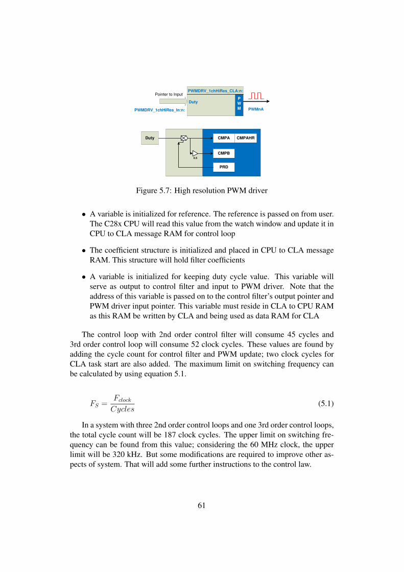
Pointer to InputPWM
Duty
PWMDRV_1chHiRes_CLA:n:
PWMDRV_1chHiRes_In:n: PWMnA
CMPA CMPAHR
CMPB
PRD
Duty
0.5
Figure 5.7: High resolution PWM driver
• A variable is initialized for reference. The reference is passed on from user.The C28x CPU will read this value from the watch window and update it inCPU to CLA message RAM for control loop
• The coefficient structure is initialized and placed in CPU to CLA messageRAM. This structure will hold filter coefficients
• A variable is initialized for keeping duty cycle value. This variable willserve as output to control filter and input to PWM driver. Note that theaddress of this variable is passed on to the control filter’s output pointer andPWM driver input pointer. This variable must reside in CLA to CPU RAMas this RAM be written by CLA and being used as data RAM for CLA
The control loop with 2nd order control filter will consume 45 cycles and3rd order control loop will consume 52 clock cycles. These values are found byadding the cycle count for control filter and PWM update; two clock cycles forCLA task start are also added. The maximum limit on switching frequency canbe calculated by using equation 5.1.
FS =Fclock
Cycles(5.1)
In a system with three 2nd order control loops and one 3rd order control loops,the total cycle count will be 187 clock cycles. The upper limit on switching fre-quency can be found from this value; considering the 60 MHz clock, the upperlimit will be 320 kHz. But some modifications are required to improve other as-pects of system. That will add some further instructions to the control law.
61

Control Filter
Pointer to Feedback
Pointer to Coeficients
CoeficientStructure
Pointer to Output
Data
Buffer
B1
B2
B3
A1
A2
A3
Dmin
Dmax
B0
ADC Result Register
Reference
Pointer to Reference
Duty Cycle
Pointer to Input
PW
M
PWMDRV_1chHiRes_CLA:n:
PWMnA
CPU to CLA Message RAM
Figure 5.8: Control loop system implementation
5.5.3 Improvements in Control Loop ArchitectureTwo modifications in the above implementation are required:
Offset Cancelation
The feedback amplifier used to amplify the current feedback has a small offset.The accuracy of current through LEDs is affected because of this offset. This off-set is needed to be removed in software. One way to solve this is to subtract theoffset value from feedback every time the control law is computed. The value ofthe offset can be measured during system initialization. A new variable is initial-ized in CPU to CLA message RAM. The control law is modified to remove thisoffset. The value is read from the variable containing the offset value and sub-tracted from the feedback value. The cycle count for the control filter is increasedby three due to this modification.
Optimization of Control Law
Drivers used from DPL are very general in nature. Several modifications can bemade:
62

• One of the limiting factors is the number of memory accesses. One wayto minimize this is by reducing the number of pointers. We propose tointegrate all the variables into one structure. Only one pointer is accessedfor the whole structure and then variables can be accessed by incrementingpointer. The sequence of instructions will be changed to make it consistentwith the newly developed variable structure.
• The memory access to the variable containing duty cycle value can be savedby integrating two drivers. Moreover, some redundant instructions in PWMdriver were removed. There are some NOP (no operation) instructions inthe code to avoid data hazards. The instructions can be better adjusted inthe integrated driver.
• Instructions are rearranged to decrease NOP count and consequently overallinstruction count.
Modified Implementation
The above mentioned modifications are made. The first modification will increasecycle count while the second one will decrease cycle count. The modified driver ispresented in appendix sections B.3. The new system implementation is presentedin figure 5.9. The new integrated driver consumes 35 clock cycles for the 2ndorder driver and 41 clock cycles for the 3rd order driver. The total cycles for fourSMPS stages will be 154 and the upper limit for switching frequency in this casewill be 388 kHz. In short, this modification was useful in increasing the switchingfrequency.
Integrated Driver
Pointer to Feedback
Pointer to Input struct
Inp
ut S
truc
ture
B1
B2
B3
A1
A2
A3
Dmin
Dmax
B0
ADC Result Register
Reference CP
U to
CL
A M
es
sa
ge
RA
M
Offset
P
WM
PWMnA
Figure 5.9: Modified control loop system implementation
63

5.5.4 Control Loop TriggeringThe CLA tasks can be triggered by ADC end of conversion, PWM module orby software. Due to limitations on sampling instants, the control law will betriggered when ADC will complete conversion. The ADC start of conversion isin turn triggered by the PWM module. Since this sampling instant is in middle ofPWM on cycle, this is configured in the initialization of the PWM module. Task1,2,3,4 are triggered using the above setup. Task 8 consists of initialization codeto be run by the CLA. So task 8 is triggered by user in software once on systemstartup. A detailed time line diagram of this is presented in figure 5.10.
△X represents the time from start of conversion to PWM update by controlloop. There are two versions of control filter as described in earlier sections. Letus denote the time for the 2nd order control loop with △X1 and the 3rd ordercontrol loop with △X2. Both these notations will be used later. △OVP gives thetime from start of conversion to computation of output by the CLA task.
PWM
ADC Acquisitionwindow
ADCComputation
Window CLA TaskComputation Time
CLAInterrupt
OVP
PWMUpdate
X
Start of Convertion
GUI & Veriable Update
Figure 5.10: Computation sequence of control loop
Since four SMPS stages are controlled with one CLA, time sharing is used toallocated 1/4 of bandwidth to each control loop. Moreover, due to requirementson sampling instants discussed in section 5.3, this time sharing is desired becauseof single shared ADC and CLA resource. Consequently, the PWM waveformscontrolling these SMPS are synchronized and phase shifted by 90 degrees. Thisscenario is shown in figure 5.11.
64

Boost1 PWM
X1
X1
X1
X2
Boost2 PWM
Buck PWM
Sepic PWM
2700
1800
900
Start of Conversion
Total time for 4 Control Loops
Figure 5.11: Time line diagram of four control loops running on CLA
5.6 C28x CodeC28x, the main CPU, is assigned to monitoring system variables and diagnostics.Important system parameters need to be monitored. This does not only have con-siderable importance in development phase, but also in final product. Consideringa final product, some of these parameters are periodically logged in ECU for lateranalysis in case of failure. There also exist a number of input parameters that areneeded to be passed to system by user. Some of them are used in control loop,i.e., reference. Some will be used by diagnostic functions. In this design phasewe used watch windows functionality available in CCS as GUI. The firmwarefor this is organized in a number of nested state machines. There is one centralstate machine which will continuously check triggering conditions for nested statemachines. This is shown in figure 5.12
State machine A, B, C is triggered by overflow of timer 1, 2, 3, respectively.Dimming state machine will be triggered by a VTimer0[0] reaching user definedvalue, which is a software timer based on timer 1 overflow. A number of func-tions exist inside each loop that are allowed to execute one by one using a statepointer concept. The detailed implementation is presented in Main.c in appendixB.1. Function-updating input parameters are organized in different loops based
65

TIMER 1OVERFLOW
VTimer0[0]++
YES
NO TIMER 2OVERFLOW
YES
NO TIMER 3OVERFLOW
YES
NOVTimer0[0]==N
YES
NO
StateMachine A
StateMachine B
StateMachine C
DimmingState
Task A0
Task B0 Task A0 Dimmimg
Initialization
Figure 5.12: C28x software architecture overview
on their update requirement and loop repetition frequency. Using the right loopfor a certain parameter is important, because of bandwidth limitations; bandwidthis a valuable resource in such MCU implementations. The details of each state ispresented in subsequent sections.
A State Machine
TASK C0
State A1
State A2
SP=&A2SP=&A1
SP=&A2 SP=&A1
Triger State Execution based on
State Pointer(SP)
Timer 1Overflow ? State Machine Exit
State Machine
Entry
YES
NO
Figure 5.13: State Machine A
State machine A is based on timer 1 which has a period of 1 ms. One of the statesis executed whenever this state machine is triggered. Since there are two tasks
66

in state machine A, the internal state will have a periodicity of 500 Hz. This isgraphically presented in figure 5.13. The actions performed in each task are listedbelow.
• State A1: First, the global power enable input from user is monitored andthe main power FET is controlled accordingly. Second, the voltage refer-ence variables for over-voltage protection are updated.
• State A2: This clears the current reference variables in case of trip zoneevents. Trip zones are activated automatically by the over-voltage functionin case over-voltage condition is detected at any of converter.
B State Machine
Timer 2Overflow ?
SP=&B2
SP=&B3 SP=&B4
SP=&B5
SP=&B1
SP=&B1
SP=&B2 SP=&B3
SP=&B4
SP=&B5
State Machine Exit
State Machine Entry
Figure 5.14: State Machine B
State machine B is based on timer 2 which has period of 2 ms; the same as forstate machine A. Since there are five tasks in state machine 5, the internal stateswill have periodicity of 100 Hz. This is graphically presented in figure 5.13.
• State B1 updates the values of input current and voltage to GUI
• State B2 performs two function
– First, values of SEPIC output current and voltage are updated on GUI
– Secondly, output current reference value is updated to CLA from GUIas user input
• State B3 performs same functions as state B2 for Boost1 converter
67

• State B4 performs same functions as state B2 for Boost2 converter
• State B5 performs same functions as state B2 for Buck converter
C State Machine
State machine C is based on timer 3, which has a period of 200 ms. There are twotasks in state machine C, so the internal states will have a periodicity of 2.5 Hz.This is graphically presented in figure 5.13.
• State C1 is just used to blink LED on the control stick to show execution ofcode
• State C2 is used to clear PWM trip zones in response of user input. Tripzones are required to be cleared to resume normal operation after a shutdown in response of an over-voltage condition.
TASK C0
State C1
State C2
SP=&C2SP=&C1
SP=&C2 SP=&C1
Triger State Execution based on
State Pointer(SP)
Timer 3Overflow ? State Machine Exit
State Machine
Entry
YES
NO
Figure 5.15: State Machine C
Dimming State
Dimming functions are driven by software timer VTimer0[0], which in turn isdriven by timer 1. 50 ticks are counted to trigger dimming. That means repetitionfrequency will be 20 Hz. This state is employed for two purposes:
• It is used to enable or disable ISR that is handling dimming functionalitybased on user input
• The dimming duty cycle is updated from GUI to PWM registers
The architecture of the dimming task is depicted in figure 5.16. Dimming isonly implemented for three converters, i.e., boost, buck-boost, and SEPIC, be-cause of availability of only three free PWM modules. Other considerations fordimming are discussed in section 5.7.
68

En_Dim = 1 ?
YES
NO
Boost1_dim = 1
Dimming DutyUpdate from
GUI(User Input)
Dimming
Enable Boost 1
Dimming
Enable Buck-
Boost
Dimming
Enable SEPIC
Enter
EXIT
EnableDimming
YES
NO
Figure 5.16: Enable dimming task architecture
5.7 PWM DimmingAn important characteristic of LED light is that current is converted into light. De-creasing current through LEDs will decrease light intensity in headlights. How-ever there are two limitation with this technique. A specified wavelength emittedby an LED is at a certain current and the wavelength will change a little if thecurrent is higher or lower than the specified current [10]. That means a changein average current through the LEDs will change the color, which is not desirablein the case of automotive headlights and the associated commercial regulations.Since SMPS are used to control the LED automotive headlights, the current inthe LEDs can be controlled by changing the duty cycle. However, at lower dutycycles these SMPS operate in discontinuous conduction mode (DCM) instead ofcontinuous conduction mode (CCM). We want our converters to operate in CCMas it is part of specifications. So the concept of PWM dimming will be employed.The full range of dimming can be used by using PWM dimming while operatingin CCM. To implement PWM dimming in this configuration, a FET is introducedin the circuit along with the grounding path. Figure 5.17 shows this configuration.
The dimming PWM signal will be derived at much lower frequency as com-pared to the main PWM. One important point to be noted is that the main PWMshould be turned off during the off time of dimming PWM to avoid voltage andcurrent spikes, which could be dangerous for the hardware platform. Moreover,based on same arguments, both PWM edges should be synchronized. The outputtripping feature available in ePWM modules in TMS32F28035 is used for thisimplementation. Tripping is a protection feature in which the ePWM output pincan be pulled to low, high or high impedance state. The trip zone can be trig-
69

LED
Load
Dimming
FET
TMS320F28035
Figure 5.17: Circuit Description of Dimming
gered from software or from hardware using external GPIO pin. Please note thatwhen the trip zone is triggered, the GPIO pin corresponding to a PWM moduleis disconnected from the PWM module while the module still keeps on runninginternally. The trip zone will be triggered for the main PWM, when the dimmingFET is switched off by dimming PWM signal. Similarly, the trip zone for the mainPWM is cleared when the dimming FET is turned on. There are two importantconsiderations related to implementation:
5.7.1 Limitation IA high level of synchronization is required between both PWM modules. This isachieved by using PWM interrupts. But there is a issue of delay between trigger-ing and execution of Interrupt Service Routine (ISR). This is handled by triggeringISR well before the PWM edge. This is possible by the help of a second compareregister available in the ePWM Module. This behavior can be clearly understoodby figure5.18.
One could argue that the main PWM will turn off or on before dimming PWM.This situation will not create any voltage or current spikes. The dimming task isgiven precedence over other CPU tasks by using ISR for implementation. Butthere are other ISRs which also have critical importance, like the one discussed insection 5.8.1, which could alter this synchronization between ISR execution andPWM edge. Relative priorities between ISRs is a trade off.
Before moving further, it is good to summarize the actions taken in ISR:
• Trip the main PWM when dimming PWM goes low and vice versa
• Interrupt source has to change from rising edge to falling edge or vice versain each ISR call
• Compare B register in PWM module has to change so that we always triggerthe interrupt well before the PWM edge
70

Compare
B
Register
Compare
A
Register
Time Base
PWM Counter
Interrupt Service
Routine Trigger
Dimming PWM
Figure 5.18: Triggering of ISR handling dimming function
5.7.2 Limitation II
Figure 5.19: Screen shot of dimming
71

As discussed before, the PWM module is running while trip zone is activated.That means the ADC is triggered periodically by PWM, which in turn will triggerthe CLA task. In short, the control loop is compensating during the off cycleof dimming PWM. During the off cycle of dimming PWM, the current throughLEDs will fall to zero, consequently feedback will fall to zero. The CLA willcompensate this by increasing the PWM duty cycle until it reaches the maximumallowable value. Remember that the PWM module’s output is disconnected fromGPIO pin and the CLA is only updating the PWM compare register. As soonas this trip zone is cleared by ISR in the on cycle of dimming PWM, this PWMwith maximum duty cycle is applied to the SMPS stage, which will respond byincreasing its output. So there will be a large current rise. A screen shot fromreal measurement is presented in figure 5.19. The curve in green and blue showcurrent and voltage respectively.
This high current will eventually be compensated by the control loop but thishas two drawbacks: First, this needs considerable time and, secondly, such a highcurrent can decrease the lifetime of LEDs and other components on the EVM. Anumber of solutions for this are implemented and tested until we came across themost suitable one. All of them are discussed here:
• The first option is to let PWM and CLA run as they are. There will be highrush current on the rising edge of the dimming PWM so this option is notfeasible.
• The next obvious option is to try to restrict the duty cycle. First the currentreference to the CLA is switched to zero during the off time of the dimmingPWM and back to the original in on time. The duty cycle will drop duringthe off time and has to rise during the on time; this will require an extremelyfast compensation.
• Next, the maximum duty cycle was fixed to a pre-conceived value so thatwhen it is increased by the CLA, it will be ceiled to that value and couldnot increase further. This implementation performed better than the aboveproposals but it has its own drawbacks. The pre-conceived maximum dutycycle suitable for best performance is dependent on the DC operating point.
• The conclusion that can be improvised from the previous implementationis that the duty cycle should be fixed to the value just before turning offthe dimming PWM as this will have fastest response as a head start willbe given to the compensator as well. This technique is implementated andtested to give the best response.
72

Figure 5.20: Screen shot of dimming after improvements
Just to summarize the above discussion, the last technique is the best amongall to implement PWM dimming. There are a number of possible alternatives toimplement this, but the simplest one is chosen, that is, by disabling the corre-sponding CLA task. This is done by disabling the corresponding ADC interrupt,which is used for triggering that CLA task. Other CLA tasks are executing andwill not be affected. A screen shot using this technique is shown in figure 5.20.The output current and voltage is shown in red and blue, respectively. This mea-surement is done with a relatively slow compensation; that is why there are someripples in the start, but it compensates after some time. The time taken by com-pensation defines the upper limit on the dimming frequency. The source code forthis is presented in section B.5
5.8 DiagnosticsThe next important part of software implementation is the diagnostics. Thesefunctions are important for the protection of the hardware platform. Considerablesystem bandwidth is however needed to be allocated to these functions. An initial
73

implementation analysis is done for allocation of bandwidth to different diagnosticfunctions. Post-implementation analysis is useful in verification and modificationof pre-implementation analysis.
5.8.1 Over-Voltage ProtectionOver-voltage protection is the most important diagnostic function. An over-voltagecondition not handled in the specified time period could result in damage to hard-ware. The bandwidth for the over-voltage protection (OVP) function is a majortrade-off:
• A high repetition rate for over-voltage check will result in suffocation ofother CPU tasks.
• Too low repetition rate can expose the EVM to over-voltage condition forlong-enough that can result in damaging EVM.
A detailed time-line diagram of the control loop implementation is presentedin figure 5.10. ADC acquisition and computation times are constant for a specificconfiguration of the project. The execution time for the CLA task is dependent onthe number of instructions, which are in turn dependent on the complexity of thecompensator.
First Draft Implementation
In the first implementation the over-voltage check is made in every CLA taskISR. The repetition rate for OVP is the same as the switching frequency. Thisimplementation is really fast, but consumes a lot of bandwidth. The details of thisimplementation are shown in figure 5.21.
Second Draft Implementation
The initial post-implementation analysis of OVP showed that the rate of increaseof voltage is low enough to allow the repetition rate of OVP to be reduced tofree system bandwidth. Secondly, every ISR takes considerable clock cycles forcontext saving. So we propose that instead of checking over-voltage condition foreach topology in its own ISR, an over-voltage condition for all channels can bechecked in one function. The ISR of the last CLA task in the whole time-line isused to implement this global OVP function. The repetition rate of OVP is thesame as before. A considerable number of clock cycles initially lost in contextsaving were saved by combining four ISRs in one. This second implementation ispresented in figure 5.22
74

Boost1 PWM
OVP
OVP
OVP
OVP
Boost2 PWM
Buck PWM
SEPIC PWM
CLA TASK 1ISR Checks
OVP for Boost1
CLA TASK 2ISR Checks
OVP for Boost2
CLA TASK 1ISR Checks
OVP for Buck
CLA TASK 1ISR Checks
OVP for SEPIC
o
o
o
Figure 5.21: Over-voltage protection implementation I
Timing Analysis
A screen-shot from real measurements is shown in figure 5.23. A time analysisis carried out for the OVP task based on this. The purpose of this is to find lowerlimits on repetition rate for OVP. The delay between two consecutive OVP checksin the first implementation was 3µ s. The measurement showed that the maximumrate at which voltage can increase under over-voltage condition is 17 kV/s. Notethat this value is dependent on the response time of compensation and independentof OVP implementation. First, the voltage increase between two consecutive over-voltage checks will be calculated
Voltage increase in 1 s:
V = 17kV (5.2)
Voltage increase in 3 µ s:
V = (17× 103)× (3× 10−6) = 0.051V (5.3)
So the voltage increase between two consecutive over-voltage checks is 0.051V which is a very moderate value. This analysis gives the liberty to decrease therepetition frequency of over-voltage checks to free the bandwidth for other tasks.
75

Boost1 PWM OVP
OVP
OVP
OVP
Boost2 PWM
Buck PWM
SEPIC PWM
CLA TASK 4This ISR ChecksOVP for Boost1,Boost2, Buck,
SEPIC
o
o
o
Figure 5.22: Over-voltage protection implementation II
Calculation for a minimum repetition rate for OVP is valuable information andvery useful for further improvement in bandwidth allocation.
Consider x V as the maximum voltage that could be allowed to increase be-tween two consecutive over-voltage checks. Then the rate of voltage change is:
△S =1sec
17× 103V= 5.88× 10⁻⁵ sec
V(5.4)
For voltage x V, value will be
△Sx = x× 5.88× 10⁻⁵sec (5.5)
The lower limit on repetition rate depends on the variable x. A power con-verter is designed to withstand certain maximum voltage. Moreover, circuit havea tolerance limit i.e. circuit can avoid catastrophic failure for certain voltage abovemaximum operating voltage. However, circuit can only with stand this voltage forcertain time. When using over voltage protection as periodic software check. The
76

Figure 5.23: OVP screen shot for boost SMPS
repetition frequency of this check determine the response time of system. So volt-age above maximum operating voltage becomes an important factor. x representsthe voltage above maximum operating voltage that could be allowed to increaseto avoid any component failure between two over voltage checks.
77

Chapter 6
Measurement and Results
The frequency-response analysis is a measure to verifying performance of a sys-tem. This analysis exposes system behavior in terms of gain and phase with fre-quency. Primarily, there are two types of tests. First, the open-loop test; as thename implies, this is carried out by opening the feedback loop. This test pro-vides information on system behavior without effect of compensator. Second, theclosed-loop test; this test is done with the feedback loop intact. This test providesinformation on the combined behavior of compensator and converter. The purposeof closed-loop tests is to compare post-implementation system behavior with themodels used during design. This comparison provides some important insightsinto digital power management tradeoffs. Both types of measurements will becarried out on our system and details about measurement setup is discussed indetail in subsequent sections.
6.1 Measurement EquipmentThe Venable Windows software in combination with the supported FrequencyResponse Analyzers (FRA) is a complete frequency-response modeling and mea-surement system [5] that is used for measurements in this project. The hardwareportion consists of the 3235 FRA, which is used for making measurements ofgain, phase, and voltage versus frequency, and various accessories for couplingthe FRA to the electrical system under test. The software portion runs on any per-sonal computer. The 3235 FRAs are controlled through a National InstrumentsGPIB board. This software also contains a simple SPICE-like modeling programfor modeling the AC frequency response of circuits. Implementation model re-sults and test results are in the same format and can be displayed simultaneouslyfor easy comparison. Compensation amplifier synthesis software lets the userachieve the exact feedback loop bandwidth and phase margin. Math software
78

allows any kind of mathematical function on any one or two transfer functions.Graph types supported are voltage versus frequency (log-log), gain and phaseversus frequency (semi-log), reactance versus frequency (log-log with lines forconstant capacitance and inductance), and Nyquist (log outside of the unity gaincircle and linear inside the unity gain circle). The FRA has a simple interface thatconsists of an oscillator, channel 1 and channel 2. The oscillator provides the ACsignal and the DC bias. Channel 1 input serves as primary input, while channel 2input serves as reference input [5].
6.2 Open-Loop MeasurementsThe open-loop transfer function refers to the gain from the output of the erroramplifier to the output of the system. This gain block typically has a fixed low-frequency gain. The high-frequency gain falls off at a -1 (-20 dB/decade) or -2(-40 dB/decade) slope depending on the characteristics of the circuit. Because thegain at low frequency (including DC) is fixed, it is possible to use a DC voltage tobias the operating point to achieve the desired system output. By superimposinga small AC voltage on the DC bias voltage, the operating point of the modulatorcan be varied. The transfer function of this gain block can then be measured byconnecting frequency selective voltmeters (the inputs of the FRA) to the input andoutput of the circuit and sweeping the modulation frequency across the desiredfrequency range. The output of the Venable 3235 FRAs are designed to deliverDC and swept frequency AC voltage simultaneously. The inputs are designed tomeasure voltage at the frequency of the output and reject all other frequencies andDC [5].
The first step is the setting up of circuit to be controlled by FRA that is done bybreaking up the feedback loop and connecting the oscillator (channel 1, channel2) at appropriate points. There are three ways these terminals can be connecteddepending on the error amplifier. Please note that none of these methods is suitablefor a digital controller. These are just mentioned to give a preview of the problem.
79

6.2.1 Method I
Figure 6.1: Open-loop measurement circuit setup I [5]
If the error amplifier is a high output impedance transconductance amplifier, theoutput can be biased high and the output of the FRA used directly to control theoperating point [5]. This setup is shown in figure 6.1.
6.2.2 Method II
Figure 6.2: Open-loop measurement circuit setup II [5]
If the error amplifier has a conventional low-impedance output but has an inputcommon-mode range at least equal to the voltage swing needed in the output tocontrol the system, the error amplifier can be wired as a buffer follower. Thissetup is shown in figure 6.2.
80

6.2.3 Method IIIIf the error amplifier has a conventional low-impedance output and a relativelynarrow input common-mode voltage range that does not encompass the entireoutput voltage swing required, the error amplifier can be wired as a gain stage andthere is complete freedom of operating point. If in doubt, this third method willwork in any situation. This third method is shown in figure 6.3.
Figure 6.3: Open-loop measurement circuit setup III [5]
6.2.4 Digital Controller Measurement Setup
Feedback
Du
tyC
yc
le
Y1
Y2
X1 X2
X
Figure 6.4: Open loop gain for buck converter
81

The measurement setups mentioned are not valid for a digital controller, asthey rely on injecting a signal either after error amplifier or before it. In the caseof a digital controller, the error amplifier is hidden in the software implementationso there is no connection to it. The scenario in which noise is injected before theerror amplifier and after the feedback is valid. Furthermore channel 1 is alwaysconnected after the error amplifier which is not possible. A modification is re-quired to get a new test setup. Since we only have a feedback pin available as aninterface to the digital controller, reference values are also provided by software.This can be solved by developing a new firmware component that can translatefeedback value to duty cycles based on the compensator’s characteristic behavior.The operating point is also needed to be adjusted in software. A curve betweenfeedback and duty cycle is plotted by empirical testing using a closed-loop imple-mentation. Please note that this graph is plotted with only a few points in proxim-ity of the Q point. Two points are chosen before and after the Q point as shownin figure 6.6. Assuming linearity of the graph around the Q point, the feedbackto duty cycle translational factor is equal to the slope of the curve. Moreover theoperating point is achieved by transept. Since we intend to provide the operatingpoint in software, the duty cycle of a point before the Q point is taken as transept.The slope can be given as
Slope = M =Y2 − Y1
X2 −X1
(6.1)
The general slope transept equation can be given as 6.2. This is modified to getequation 6.3. The term Y1 is a duty cycle value and will serve as DC offset. Theterm FeedBack −X is used rather than only Feedback so that the output canoscillate about the Q point. Firmware is developed to implement this equation.Please note that this technique is applied to all converters to get their values ofslope and DC-offset. Consequently, firmware is developed for each converter.
y = C +M ×X) (6.2)
DutyCycle = Y1 + Slope× FeedBack −X (6.3)
The feedback loop is broken to setup hardware for open-loop measurements.Noise is injected on one side and the response is measured on the other side. Fig-ure 6.5 shows this setup. The loop can be broken either before the feedback am-plifier or after it. In both cases, measurement is valid. The oscillator and channel1 are coupled and connected to the noise injection point. Channel 2 is connected
82

on the other side so as to measure system response. There is an important con-sideration in this regard that input and output points lie in close proximity; gainwill very low for such setup. This technique for open-loop measurement for digi-tal power controller based converter is improvised but need further analysis. Thedetails of software implementation can be found in C for buck, boost and SEPICconverters. The DC bias needed to operate on desired Q point is provided primar-ily by software. A small value is also introduced from FRA so as to fine tune theQ point. An AC value of the noise signal is selected so that feedback could notexceed points X and Y, because our translational factor and transept is only validin this region.
Feedback
Amplifier
Channel 1 Channel 2Oscilator
Feedback loop is
broken from here
Figure 6.5: Open-loop measurement setup
83

6.2.5 Measurement Results
Frequency10 250 k
10 H
z
100 H
z
1 k
Hz
10 k
Hz
100 k
Hz
Ga
in-8
00
Ph
ase
-36
00
-75 dB
-70 dB
-65 dB
-60 dB
-55 dB
-50 dB
-45 dB
-40 dB
-35 dB
-30 dB
-25 dB
-20 dB
-15 dB
-10 dB
-5 dB
-337.5 deg
-315 deg
-292.5 deg
-270 deg
-247.5 deg
-225 deg
-202.5 deg
-180 deg
-157.5 deg
-135 deg
-112.5 deg
-90 deg
-67.5 deg
-45 deg
-22.5 deg
1-Gain
1-Phase
Figure 6.6: Open-loop gain for buck converter
The detailed implementation of firmware for the open-loop test for the buck con-verter is shown in C. The code for other converters is similar with different val-ues of DC-offset and slope factor. The bode plot of measured open-loop transferfunction for buck, boost and SEPIC is shown in figures 6.6, 6.7, 6.8, respectively.Phase and gain scaling with frequency is provided in two separate graphs. Thephase response of all the converters is consistent with modeling results with mi-nor deviations. This can be explained by tolerance in components used on thePCB. The gain response differs largely from expected, from the modeling results.This is due to fact that in our setup CH1 and CH2 are connected at the same point.Theoretically, the gain should be zero at low frequencies in our case. However,the low-frequency gain in our case is around -5 dB. This minor deviation can beexplained as a shortcoming in the data representation because existing data repre-sentation has its roots in analog control measurements. Moreover, this setup foropen-loop measurement is new and needs further refinement. In short, develop-ment and use of this test gives valuable insight into digital controller performancemeasurements setups. However, new analysis techniques are needed to fully ex-ploit capabilities of this test.
84

Frequency1 1 M
1 H
z
10 H
z
100 H
z
1 k
Hz
10 k
Hz
100 k
Hz
Ga
in-8
00
Ph
ase
-36
00
-75 dB
-70 dB
-65 dB
-60 dB
-55 dB
-50 dB
-45 dB
-40 dB
-35 dB
-30 dB
-25 dB
-20 dB
-15 dB
-10 dB
-5 dB
-337.5 deg
-315 deg
-292.5 deg
-270 deg
-247.5 deg
-225 deg
-202.5 deg
-180 deg
-157.5 deg
-135 deg
-112.5 deg
-90 deg
-67.5 deg
-45 deg
-22.5 deg
2-Gain
2-Phase
3-Gain
3-Phase
Figure 6.7: Open-loop gain for boost converter
Frequency1 1 M
1 H
z
10 H
z
100 H
z
1 k
Hz
10 k
Hz
100 k
Hz
Ga
in-1
00
0
Ph
ase
-35
01
0
-90 dB
-80 dB
-70 dB
-60 dB
-50 dB
-40 dB
-30 dB
-20 dB
-10 dB
-314 deg
-278 deg
-242 deg
-206 deg
-170 deg
-134 deg
-98 deg
-62 deg
-26 deg 1-Gain
1-Phase
Figure 6.8: Open-loop gain for SEPIC converter
85

6.3 Closed-Loop Measurement
Figure 6.9: Classical method for measuring frequency response [5]
The digital control loop implemented is verified by closed-loop measurements.The classical way to measure a feedback loop transfer function is to break the loopat some point, terminate the input with the output impedance, terminate the outputwith the input impedance, drive a small AC signal into the input and measurethe ratio of the output to the input. In real life, this measurement approach isvirtually impossible since the loop gain is usually very high at low frequency andit is difficult to keep the input stable enough to prevent the output from swingingwildly from limit to limit. The classical approach is presented in 6.9 while theVenable approach is presented in figure 6.10.
86

Venable Method
Figure 6.10: Venable method for measuring frequency response [5]
This difficulty in the measurement situation is avoided by finding a placewhere the loop is confined to a single path (also a requirement in the classicalmethod) and a place where the signal comes from a low-impedance point anddrives a high-impedance point. This impedance condition minimizes the errorcaused by not properly terminating the input and output. We then insert a small re-sistor into the feedback loop (small compared to the input impedance of the loop).Finally, we connect a floating AC source (the output of a transformer) across thenew resistor and drive the primary of the transformer with a sinusoidal voltagesource. This converts the resistor into a floating sinusoidal error voltage in serieswith the feedback loop. This voltage modulates the operating point of the entirecircuit [5]. In the context of a digital implementation, this single path is availablebetween the feedback amplifier and the ADC channel. This setup for closed-loopmeasurement is presented in figure 6.11. Noise will be injected over a resistor inthe feedback loop using the injection transformer (BodeBox) as mentioned above.
The feedback loop measurement for boost and buck converter is shown infigure 6.12 and 6.13, respectively. The phase response is consistent with com-pensator model. Minor deviations are there due to component tolerance as thecompensator model is based on an ideal converter model that assumes ideal com-ponents. The gain response is different because of the same reasons explainedbefore in section 6.2.5.
87

Feedback
Amplifier
Channel 1 Channel 2Oscilator
Permutation is
injected in feedback resistor
MeasurementTransformer
Osc Ch1 Ch2
R
Figure 6.11: Closed-loop measurement setup
Frequency1 1 M
1 H
z
10 H
z
100 H
z
1 k
Hz
10 k
Hz
100 k
Hz
Ga
in-6
06
0
Ph
ase
-18
01
80
-50 dB
-40 dB
-30 dB
-20 dB
-10 dB
0 dB
10 dB
20 dB
30 dB
40 dB
50 dB
-150 deg
-120 deg
-90 deg
-60 deg
-30 deg
0 deg
30 deg
60 deg
90 deg
120 deg
150 deg
1-Gain
1-Phase
2-Gain
2-Phase
Figure 6.12: Boost feedback loop measurement
88

Frequency100 100 k
100 H
z
1 k
Hz
10 k
Hz
Ga
in-4
04
0
Ph
ase
-36
00
-35 dB
-30 dB
-25 dB
-20 dB
-15 dB
-10 dB
-5 dB
0 dB
5 dB
10 dB
15 dB
20 dB
25 dB
30 dB
35 dB
-337.5 deg
-315 deg
-292.5 deg
-270 deg
-247.5 deg
-225 deg
-202.5 deg
-180 deg
-157.5 deg
-135 deg
-112.5 deg
-90 deg
-67.5 deg
-45 deg
-22.5 deg
1-Gain
1-Phase
2-Gain
2-Phase
Gain1--Buck close loop
Figure 6.13: Buck feedback loop measurement setup
89

6.4 Hardware Platform ImprovementThere are issues that are exposed after the firmware development on the EVM.Improvements are required in the EVM to improve performance. Moreover, thereare some suggestions regarding improvements in the micro-controller. The pro-posed improvements in EVM are closely concerned with this project. However,they also have a general perspective as well, general to similar applications.
Consequent ADC Triggering
While dealing with real-time applications, it’s important to have a deterministicanalysis of different software tasks. This will help to have an accurate timing anal-ysis. Moreover, a discrete system implementation is required to sample feedbacksignal at particular instants as discussed in section 5.3. This adds further impor-tance to deterministic timing analysis. Non-critical signals, i.e., output voltages,are sampled in time slots between sampling of critical signals, i.e., output cur-rents. For example, in the boost converter all the non-critical signals are sampledafter sampling output current feedback. These conversions should be completebefore the buck-boost converter requests sampling of its current feedback. Anideal scenario would be to start ADC conversion of non-critical signal from endof conversion (EOC) signal of critical one. In general, an EOC should trigger astart of conversion (SOC). That means simply routing EOC signal of one SOCto start another SOC. Unfortunately this is not possible. A technique based onpolling and priority is used instead.
Summarizing the above discussion, a functionality of triggering start of con-version of SOC from EOC of another one is needed. This is not available on thisTMS320F28035 MCU. This capability will increase the deterministic analysis ofreal-time applications. From a hardware design’s perspective, a few multiplexesare required in the signal routing path. That will not have a significant overheadbut yield a far better application analysis.
Inductor and Output Current feedback
In current mode, it is required to sample output current and inductor current valuesat same time due to reasons discussed in section 5.3. There are two sample andhold circuits in TMS320F28035. But simultaneous sampling is only possible withpair of channel one from each group, i.e., group A and B. That means A0 can onlybe simultaneously sampled with B0. This implies that the output current feedbackshould be connected to A0 and the inductor current feedback should be connectedto B0 for any converter. Our EVM does not not support this connection as thislimitation was not known at the time of board development. It is suggested to
90

improve EVM to have these connections. However, the MCU can also be modifiedin future versions to remove this limitation in hardware.
91

Chapter 7
Conclusion
Voltage-mode control for a converter driving LEDs poses some limitations ondigital controllers. First, this technique is an indirect way to control current. Theaccuracy of the controlled parameter, i.e., the current, is considerably low. Sec-ondly, the converter models used in this technique are complex, requiring a com-plex compensator of the same order. This fact poses limitations on switching fre-quency. A limited improvement in switching frequency can be made by optimiz-ing firmware but this technique has some inherent limitations. These convertersare inherently non-linear and averaging approximations are applied to develop lin-ear counterparts. These approximations are based on small signal linearity arounda large signal operating point (Q point). We used these linear continuous-timemodels to develop discrete-time non-linear models, again by using some approx-imation. This approach can be summarized as, first continuous-time linear mod-els are developed for non-linear converters and later these continuous-time linearmodels are converted to discrete-time models. Considerable system behavior in-formation is lost because of approximations used at both transitions.
A direct approach to problem should be employed. Techniques based oncurrent-mode control are better suited for driving LEDs. Such techniques arebased on current injection control that uses the fact that current injected into aninductor from input during the PWM on cycle will end up in output (with somepre-known scaling factor). This technique can increase the accuracy of the con-trolled parameter (current). Moreover, it can significantly reduce the complexityof the compensator. But these techniques also require a transformation from ex-isting continuous-time models to discrete-time models.
A discrete-time non-linear control developed directly for these converters wouldcertainly perform better. First, it can depict the exact behavior of system and noneof the system behavior is lost in approximations. Secondly, one of the advan-
92

tages of digital power management is that it is very easy to implement non-linearcontrol algorithms when compared with analog solution. Advantages of this ca-pability can be fully reaped by using non-linear model to control power stages.Lastly these non-linear models are far less complex and a compensator for themcan be realized using far less instructions. That, consequently, increases the up-per limit on switching frequency. Switching frequency is a major limitation whencompared to analog controllers. In short, use of such models will improve over-all performance of digital power management solutions and enable them to reallychallenge analog counterparts. Unfortunately little work has been done in this re-gard.
The proposed current control model is based on same motivations. It is anon-linear discrete-time model proposed in the context of LEDs. There are twoconsiderations in this regard. First, this uses the current mode control techniquebased current injection. Secondly, this model depicts non-linear behavior of con-verters. The behavior of the converter during the PWM on cycle is used to developthis model, while the PWM off cycle is not considered as it has no effect on thevalue of the output current. This modeling technique was only applied to theboost converter in our report. This model needs refinement and verification as itjust proposed a way forward.
Some of the measurement techniques currently being used for analog controlloop measurements cannot be directly employed for digital controllers. A newtest setup is proposed to measure open-loop transfer functions for digital con-trollers. This test-setup performed really well and results are verifiable. But it canbe further refined. The existing test setup is used for closed-loop method. Bothopen-loop and closed-loop measurements verified the models developed earlierwith some limitation. Further work is suggested in improving test setups. Furtherwork is suggested in transforming and interpreting well-known existing test se-tups for analog controllers to digital controllers.
This discussion can be concluded by a evaluation of TMS320F28035 MCUfor such power control applications. This MCU is optimized for real-time controlapplications and offers two distinct features to support digital power control ap-plications. First, a floating point coprocessor (CLA) is available for control-lawimplementation. Availability of two CPUs increases the performance consider-ably by increasing system bandwidth. Moreover, integration of powerful analogperipherals like ADC, PWM and comparator modules further enhances the ca-pabilities. However, a number of limitations and improvements are discussed in6.4. In short this controller is a complete package for digital power managementsolutions.
93

94

Bibliography
[1] Headlamp without Optics Datasheet (LE UW D1W1 01 OSTAR), osramSemiconductor. [Online]. Available: http//:www.osram.com
[2] M. Day, “LED-driver considerations,” 2004. [Online]. Available:http://www.ti.com/sc/analogapps
[3] TMS320F28035 Data Sheet. [Online]. Available: http//:www.ti.com
[4] E. Rogers, Understanding Boost Power Stage in Switch Mode Power Stages(SLVA061), March 1999.
[5] Using the Venable Windows Software Version 4 for Models 3215/3225/3235.[Online]. Available: http://www.venable.biz
[6] “Using LEDs in Lighting,” US Department of Energy, Tech. Rep. [Online].Available: http://www1.eere.energy.gov/buildings/ssl/m/using leds.html
[7] L. Balogh, “A Practical Introduction to Digital Power Control (SLUP232),”Texas Instruments, Tech. Rep., 2005.
[8] TMS320F28035 Product Home Page. [Online]. Available:http://focus.ti.com/docs/prod/folders/print/tms320f28035.html
[9] How LEDs Work. [Online]. Available:http://www1.eere.energy.gov/buildings/ssl
[10] S. Winder, Power Supplies for LED Driving. Elsevier Inc., 2008.
[11] “Haitzs law.” [Online]. Available: http//:en.wikipedia.org/wiki/Haitz’s Law
[12] R. Lineback, “Solid State Lighting Set to Boost LED Growth,” May 2006.[Online]. Available: www.ledsmagazine.com/features/3/5/6
[13] “Hella product page,” light-Headlamps. [Online]. Available: www.hella.com
95

[14] “Visteon product specifications,” light Emitting Diode (LED) Front Light-ing.
[15] B. Flemming, “New Technologies in Electric-Powered Vehicles [Automo-tive Electronics],” IEEE Vehicular Technology Magazine, vol. 5, no. 1,March 2010.
[16] J. Betten, “Control Loop Consideration for an LED Driver,” August 2007.
[17] B.-J. Huang, C.-W. Tang, and J.-H. Wu, “Study of System Dynamics ofHigh-Power LEDs,” in International Conference on Electronic Materialsand Packaging, December 2006.
[18] D. Gacio, A. Calleja, J. Garcia, J. Ribas, and M. Rico-Secades, “SuitableSwitching Converter Topologies for Automotive Signal Lamps and Head-lamps Using Power LEDs,” in Industry Applications Society Annual Meet-ing, 2008. IAS ’08. IEEE, October 2008.
[19] E. Rogers, Understanding Buck Power Stage in Switch Mode Power Stages(SLVA057), March 1999.
[20] R. Ridley, Analyzing the SEPIC Converter, November 2006. [Online].Available: http//:www.ridleyengineering.com
[21] C2000 real time microcontroller platform. [Online]. Available:http://focus.ti.com/mcu/docs/mcuprodoverview.tsp?sectionId=95&tabId=1531&familyId=916
[22] TMS320x2803x Piccolo Control Law Accelerator (CLA)Reference Guide-Rev. B(SPRUGE6). [Online]. Available:http://www-s.ti.com/sc/techlit/SPRUGE6
[23] TMS320x2802x,2803 Piccolo Analog-to-Digital Converter and Comparator(SPRUGE5). [Online]. Available: http//www-s.ti.com/sc/techlit/SPRUGE5
[24] TMS320x2802x, 2803x Piccolo Enhanced Pulse Width Modulator(SPRUGE9). [Online]. Available: http://www-s.ti.com/sc/techlit/SPRUGE9
[25] TMS320x2802x, 2803 Piccolo High-Resolution Pulse-Width Modulator.[Online]. Available: http://www-s.ti.com/sc/techlit/SPRUGE8
[26] V. Vorperian, “Simplified analysis of PWM converters using model of PWMswitch. continuous conduction mode,” IEEE Transactions on Aerospace andElectronic Systems, vol. 26, no. 3, pp. 490 –496, May 1990.
96

[27] ——, “Simplified analysis of PWM converters using model of PWM switch.Discontinuous conduction mode,” IEEE Transactions on Aerospace andElectronic Systems, vol. 26, no. 3, pp. 497 –505, May 1990.
[28] Y.-T. Chang and Y.-S. Lai, “Effect of sampling frequency of A/D converteron controller stability and bandwidth of digital-controlled power converter,”in 7th International Conference on Power Electronics, October 2007, pp.625 –629.
[29] M. Rashid, Power Electronics Handbook. Academic Press, 2006.
[30] S. Choudhury, Designing a TMS320F280x Based Digitally Controlled DC-DC Switching Power Supply (SPRAAB3), July 2005. [Online]. Available:http://focus.ti.com/lit/an/spraab3/spraab3.pdf
[31] D. Sable and R. Ridley, “Comparison of performance of single-loop andcurrent-injection control for PWM converters that operate in both continu-ous and discontinuous modes of operation,” IEEE Transactions on PowerElectronics, vol. 7, no. 1, pp. 136 –142, January 1992.
[32] Y.-S. Jung, J.-Y. Lee, and M.-J. Youn, “A new small signal modeling ofaverage current mode control,” in 29th Annual IEEE Power Electronics Spe-cialists Conference, vol. 2, May 1998, pp. 1118 –1124.
[33] Control Suit. [Online]. Available:http://focus.ti.com/docs/toolsw/folders/print/controlsuite.html
97

Appendix A
Matlab Models
A.1 Buck
%% P l a n t P a r a m e t e r sVin = 1 2 . 0 ; % I n p u t V o l t a g eVd = 3 . 3 ; % Led Forward v o l t a g e dropN = 1 ; % No of LEDsVo = N∗Vd ; % o u t p u t V o l t a g eD= Vo / Vin ; % Optimum Duty CycleIo = 1 ; % Maximum Outpu t C u r r e n tL = 10e−6; % I n d u c t e rC = 1 4 . 1 e−6; % C a p i t o rRc = 0 . 0 3 1 ; % C a p c i t o r P a r a s i t i c R e s i s t a n c eRl = 0 . 0 4 7 ; % I n d u c t e r P a r a s i t i c r e s i s t a n c eF = 500 e3 ; % Sampl ing FrequencyTs = 1 / F ; % Sampl ing P e r i o dTd= 0.5∗Ts ; % Time Delay from Sampl ing t o Outpu t UpdateKd= 1 / 3 . 3 ;%% F a c t o r I n t r o d u c e d due t o C u r r e n t C o n t r o lRs = 0 . 0 2 ; % Shunt R e s i s t a n c e t o measure c u r r e n tRd = 0 . 8 5 ; % Led Dynamic r e s i s t a n c eR = ( Rd∗N)+ Rs ; % T o t a l Led Load Dynamic R e s i s t a n c eGamp = 3 0 ; % C u r r e n t s e n s e a m p l i f i e r g a i nGi = Gamp∗Rs / R ; % T r a n s f e r F u n c t i o n f o r Outpu t C u r r e n t t o Outpu t V o l t a g eGdc = Vin∗R / ( R+Rl ) ; % Dc f a c t o r i n T r a n s f e r f u n c t i o n%%%%%%%%%%%%%% Numerator o f Buck C o n v e r t e r T r a n s f e r F u n c t i o n %%%%%%%n1 = Rc∗C ;n0 = 1 ;num Gps = Gdc∗Gi∗[ n1 n0 ] ;%%%%%%%%%%%%%% Denominator o f Buck C o n v e r t e r T r a n s f e r F u n c t i o n %%%%%%%d2 = ( L∗C∗(R+Rc ) ) / ( R+Rl ) ;d1 = (C∗(Rc + ( (R∗Rl ) / ( R+Rl ) ) ) ) + ( L / ( R+Rl ) ) ;d0 = 1 ;denom Gps = [ d2 d1 d0 ] ; % Denominator%% C o n t i n u o s T a n s f e r F u n c t i o nGps dly Buck = t f ( num Gps , denom Gps , i n p u t d e l a y , Td ) ;%% C o n t i n u o s T a n s f e r F u n c t i o nGpz Buck = c2d ( Gps dly Buck∗Kd , Ts , zoh ) ;s i s o t o o l ( bode , Gpz Buck ) ;
A.2 Boost
%% P l a n t P a r a m e t e r sVin = 1 2 . 1 ; % I n p u t V o l t a g eVd = 2 . 9 0 6 ; % Led Forward v o l t a g e dropN = 1 0 ; % No of LEDsVo = N∗Vd ; % o u t p u t V o l t a g e
98

D= 1−(Vin / Vo ) ; % Optimum Duty CycleIo = 1 ; % Maximum Outpu t C u r r e n tL = 39e−6; % I n d u c t e rRl = 0 . 0 4 7 ; % I n d u c t e r p a r a s i t i c R e s i s t a n c eC = 30e−6; % C a p a c i t o rRc = 0 . 0 3 1 ; % P a r s i t i c R e s i s t a n c eF = 500 e3 ; % Sampl ing FrequencyTs = 1 / F ; % Sampl ing P e r i o dTd= 0.5∗Ts ; % Delay from Sampl ing t o o u t p u t u p d a t eKd = 1 / 3 . 3 ;%% F a c t o r I n t r o d u c e d due t o C u r r e n t C o n t r o lRs = 0 . 1 ; % Shunt R e s i s t a n c e t o measure c u r r e n tRd = 1 . 3 7 5 ; % Led Dynamic r e s i s t a n c eR =(Rd∗N)+ Rs ; % T o t a l Led Load Dynamic R e s i s t a n c eKamp = 2 0 ; % A m p l i f i e r g a i nGi = Rs∗Kamp / R ; % C u r r e n t f a c t o r%% P l a n t T r a n s f e r F u n c t i o nD1 = (1−D ) ˆ 2 ;Gd0 = Vin / D1 ;Wz1 = 1 / ( Rc∗C ) ;Wz2 = ( D1∗R−Rl ) / L ;Wo = ( 1 / s q r t ( L∗C))∗ s q r t ( ( Rl +(D1∗R ) ) / R ) ;Q = Wo / ( ( Rl / L ) + ( 1 / ( C∗(R+Rc ) ) ) ) ;% Numerator o f Boos t C o n v e r t e r T r a n s f e r F u n c t i o nn2 = −1/(Wz1∗Wz2 ) ;n1 = ( 1 / Wz1)−(1/Wz2 ) ;n0 = 1 ;num Gps = Gd0∗Gi∗[ n2 n1 n0 ] ;% Denominator o f Boos t1 C o n v e r t e r T r a n s f e r F u n c t i o nd2 = 1 / (Woˆ 2 ) ;d1 = 1 / (Wo∗Q ) ;d0 = 1 ;denom Gps = [ d2 d1 d0 ] ; % Denominator%% C o n t i n u o s T a n s f e r F u n c t i o nG p s d l y B o o s t 1 = t f ( num Gps , denom Gps , i n p u t d e l a y , Td ) ;%% C o n t i n u o s T a n s f e r F u n c t i o nGpz Boost1 = c2d ( G p s d l y B o o s t 1∗Kd , Ts , zoh ) ;s i s o t o o l ( bode , Gpz Boost1 ) ;
A.3 Buck-Boost
%% P l a n t P a r a m e t e r s %%%%%%%%%%%%%%%%%%%%%%%%%Vin = 1 2 . 0 ; % I n p u t V o l t a g eVd = 3 . 3 ; % Led Forward v o l t a g e dropN = 4 ; % No of LEDsVo = N∗Vd ; % o u t p u t V o l t a g eD = 1−(Vin / Vo ) ; % Optimum Duty CycleIo = 1 ; % Maximum Outpu t C u r r e n tL = 39e−6; % I n d u c t e rRl = 0 . 0 4 7 ; % I n d u c t e r P a r a s i t i c R e s i s t a n c eC = 30e−6; % C a p a s i t a n c eRc = 0 . 0 3 1 ; % C a p a c i t o r P a r a s i t i c R e s i s t a n c eF = 300 e3 ; % Sampl ing FrequencyTs = 1 / F ; % Sampl ing P e r i o dTd= 0.25∗Ts ; % Delay from Sampl ing t o Outpu t UpdateKd = 1 / 3 . 3 ;%% F a c t o r I n t r o d u c e d due t o C u r r e n t C o n t r o lRs = 0 . 1 ; % Shunt R e s i s t a n c e t o measure c u r r e n tRd = 0 . 8 5 ; % Led Dynamic r e s i s t a n c eR =(Rd∗N)+ Rs ; % T o t a l Led Load Dynamic R e s i s t a n c eKamp = 2 0 ; % A m p l i f i e r g a i nGi = Rs∗D∗Kamp / R ; % c u r r e n t f a c t o r%% P l a n t T r a n s f e r F u c t i o nD1 = (1−D ) ˆ 2 ;Gd0 = Vin / D1 ;Wz1 = 1 / ( Rc∗C ) ;Wz2 = ( D1∗(R−Rl ) ) / L ;Wo = ( 1 / s q r t ( L∗C))∗ s q r t ( ( Rl +(D1∗R ) ) / R ) ;Q = Wo / ( ( Rl / L ) + ( 1 / ( C∗(R+Rc ) ) ) ) ;% Numerator o f Buck−Boost C o n v e r t e r T r a n s f e r F u n c t i o nn2 = −1/(Wz1∗Wz2 ) ;n1 = ( 1 / Wz1)−(1/Wz2 ) ;n0 = 1 ;num Gps = Gd0∗Gi∗[ n2 n1 n0 ] ;% Denominator o f Buck−Boost C o n v e r t e r T r a n s f e r F u n c t i o nd2 = 1 / (Woˆ 2 ) ;d1 = 1 / (Wo∗Q ) ;d0 = 1 ;
99

denom Gps = [ d2 d1 d0 ] ; % Denominator%% C o n t i n u s T r a n s f e r F u n c t i o nG p s d l y B o o s t 2 = t f ( num Gps , denom Gps , i n p u t d e l a y , Td ) ;%% D i s c r e t e T r a n s f e r F u n c t i o nGpz Boost2 = c2d ( G p s d l y B o o s t 2∗Kd , Ts , zoh ) ;s i s o t o o l ( bode , Gpz Boost2 ) ;
A.4 SEPIC
%% P l a n t P a r a m e t e r sVin = 1 2 . 0 ; % I n p u t V o l t a g eVd = 3 . 3 ; % Led Forward v o l t a g e dropN = 1 0 ; % No of LEDsVo = N∗Vd ; % o u t p u t V o l t a g eD= Vo / ( Vin+Vo ) ; % Optimum Duty CycleIo = 1 ; % Maximum Outpu t C u r r e n tD1 = Dˆ 2 ; % Duty Cycle Squre f o r s i m p l i f y i n gD2 = (1−D ) ˆ 2 ; % (1−Duty Cycle ) Squre f o r s i m p l i f y i n gL1 = 15e−6; % I n d u c t e r 1L2 = 15e−6; % I n d u c t e r 2C1 = 1 4 . 1 e−6; % C a p a c i t o r 1C2 = 30e−6; % C a p a c i t o r 2F = 300 e3 ; % Sampl ing FrequencyTs = 1 / F ; % Sampl ing P e r i o dTd = 0.25∗Ts ; % Delay from Sampl ing t o Outpu t UpdateKd= 1 / 3 . 3 ;%% F a c t o r I n t r o d u c e d due t o C u r r e n t C o n t r o lRs = 0 . 1 ; % Shunt R e s i s t a n c e t o measure c u r r e n tRd = 0 . 8 5 ; % Led Dynamic r e s i s t a n c eR = ( Rd∗N)+ Rs ; % T o t a l Led Load Dynamic R e s i s t a n c eKamp = 2 0 ; % A m p l i f i e r g a i nGi = Rs∗Kamp / R ;%% P l a n t T r a n s f e r F u n c t i o nGdc = 1/((1−D ) ˆ 2 ) ;Wz1 = ( L1∗D1 ) / ( R∗D2 ) ;Wz2 = ( D2∗(L1+L2)∗R∗C1 ) / ( L1∗D1 ) ;Wz3 = ( L2∗C1 ) / D;A0 = ( L1∗C1∗C2 ) / ( ( L1∗C1)+C2 ) ;A1 = ( L2∗C1∗C2 ) / ( ( L2∗C1∗D2 ) + ( C2∗D1 ) ) ;Wo1 = 1 / s q r t ( ( L1∗ ( ( C2∗D1 / D2)+C1 ) ) + ( L2∗(C1+C2 ) ) ) ;Wo2 = s q r t ( ( 1 / A0 ) + ( 1 / A1 ) ) ;Q1 = (R∗D2 ) / ( Wo1∗ ( ( L1∗D1 ) + ( L2∗D2 ) ) ) ;Q2 = (R∗C2∗Wo2 ) / ( ( L1+L2)∗C1∗(Wo1 ˆ 2 ) ) ;% Numerator o f Boos t1 C o n v e r t e r T r a n s f e r F u n c t i o nn3 = −1∗Wz1∗Wz3 ;n2 = (Wz1∗Wz2) + Wz3 ;n1 = −1∗(Wz1+Wz2 ) ;n0 = 1 ;num Gps = Gdc∗Gi∗[ n3 n2 n1 n0 ] ;% Denominator o f Boos t1 C o n v e r t e r T r a n s f e r F u n c t i o nd4 = 1 / ( ( Wo1ˆ 2 )∗ (Wo2 ˆ 2 ) ) ;d3 = ( 1 / ( Wo2∗Q2∗(Wo1 ˆ 2 ) ) ) + ( 1 / ( Wo1∗Q1∗(Wo2 ˆ 2 ) ) ) ;d2 = ( 1 / ( Wo1 ˆ 2 ) ) + ( 1 / ( Wo2 ˆ 2 ) ) + ( 1 / ( Wo1∗Wo2∗Q1∗Q2 ) ) ;d1 = ( 1 / ( Wo1∗Q1 ) ) + ( 1 / ( Wo2∗Q2 ) ) ;d0 = 1 ;denom Gps = [ d4 d3 d2 d1 d0 ] ; % Denominator%% C o n t i n u o s T a n s f e r F u n c t i o nG p s d l y S e p i c = t f ( num Gps , denom Gps , i n p u t d e l a y , Td ) ;
%% C o n t i n u o s T a n s f e r F u n c t i o nGpz Sepic = c2d ( G p s d l y S e p i c∗Kd , Ts , zoh ) ;s i s o t o o l ( bode , Gpz Sepic ) ;
A.5 Filter Conversion Script
A.5.1 Convert.mScript for converting compensator transfer function for inputting in 2nd order filterimplemented in TMS320F28035 micro-controller.
100

Z0 = i n p u t ( E n t e r Z0 ) ;Z1 = i n p u t ( E n t e r Z1 ) ;Z2 = i n p u t ( E n t e r Z2 ) ;P1 = i n p u t ( E n t e r P1 ) ;P2 = i n p u t ( E n t e r P2 ) ;x= 2 ˆ 2 6 ;B0 = Z0∗x ;B1 = −Z0∗(Z2+Z1)∗x ;B2 = Z0∗Z1∗Z2∗x ;A1 = ( P1+P2)∗x ;A2 = −1∗P1∗P2∗x ;
A.5.2 Convert2.mScript for converting compensator transfer function for inputting in 3nd order filterimplemented in TMS320F28035 micro-controller.
Z0 = i n p u t ( E n t e r Z0 ) ;Z1 = i n p u t ( E n t e r Z1 ) ;Z2 = i n p u t ( E n t e r Z2 ) ;Z3 = i n p u t ( E n t e r Z2 ) ;P1 = i n p u t ( E n t e r P1 ) ;P2 = i n p u t ( E n t e r P2 ) ;P3 = i n p u t ( E n t e r P2 ) ;x= 2 ˆ 2 6 ;B0 = Z0∗x ;B1 = −Z0∗(Z3+Z2+Z1)∗x ;B2 = x∗Z0∗ ( ( Z3∗(Z1+Z2 ) ) + Z1∗Z2 ) ;B3 = −1∗Z0∗Z1∗Z2∗Z3∗x ;A1 = ( P1+P2+P3)∗x ;A2 = −1∗(P1∗P2+ ( P3∗(P1+P2 ) ) )∗ x ;A3 = P1∗P2∗P3∗x ;
A.6 Current Mode Control
%% P l a n t P a r a m e t e r sVin = 1 2 . 0 ; % I n p u t V o l t a g eL = 39e−6; % I n d u c t e rRl = 0 . 0 4 7 ; % I n d u c t e r p a r a s i t i c R e s i s t a n c eF = 500 e3 ; % Sampl ing FrequencyTs = 1 / F ; % Sampl ing P e r i o dTd= 0.5∗Ts ; % Delay from Sampl ing t o o u t p u t u p d a t e%% P l a n t T r a n s f e r F u n c t i o nGdc = Vin∗Ts / ( 2∗ Rl ) ;% Numerator o f Boos t C o n v e r t e r T r a n s f e r F u n c t i o nn0 = 1 ;num Gps = Gdc∗n0 ;% Denominator o f Boos t1 C o n v e r t e r T r a n s f e r F u n c t i o nd1 = L / Rl ;d0 = 1 ;denom Gps = [ d1 d0 ] ; % Denominator%% C o n t i n u o s T a n s f e r F u n c t i o nG p s d l y B o o s t 1 = t f ( num Gps , denom Gps , i n p u t d e l a y , Td ) ;%% C o n t i n u o s T a n s f e r F u n c t i o nGpz Boost1 = c2d ( Gps d ly Boos t1 , Ts , zoh ) ;s i s o t o o l ( bode , Gpz Boost1 ) ;
101

Appendix B
Firmware
This section contains complete software implementation
B.1 Main.c
# i n c l u d e ”LedDemo−S e t t i n g s . h ”# i n c l u d e ” P e r i p h e r a l H e a d e r I n c l u d e s . h ”# i n c l u d e ” DSP280x EPWM defines . h ”# i f d e f i n e d ( CLA TYPE0 )
# i n c l u d e ”LedDemo−CLAShared . h ”# e n d i f
# i n c l u d e ” DPLib . h ”
/ /%%%%%%%%%%%%%%%%%%%%%%%%%%%%%%%%%%%%%%%%%%%%%%%%%%%%%%%%%%%%%/ / FUNCTION PROTOTYPES/ /%%%%%%%%%%%%%%%%%%%%%%%%%%%%%%%%%%%%%%%%%%%%%%%%%%%%%%%%%%%%%
/ / −−−−−−−−−−−−−−−−−−−−−−−−−−−−−−−− FRAMEWORK−−−−−−−−−−−−−−−−−−−−−−−−−−−−−−−−−−−−−−vo id D e v i c e I n i t ( vo id ) ;vo id I S R I n i t ( vo id ) ;
# i f d e f FLASH
vo id I n i t F l a s h ( ) ;vo id MemCopy( Uin t16∗∗ , U in t16∗∗ , U in t16 ∗∗ ) ;# pragma CODE SECTION( c l a 1 i s r , ” r amfuncs ” ) ;# pragma CODE SECTION( Pwm3 Dim , ” ramfuncs ” ) ;# pragma CODE SECTION( Pwm6 Dim , ” ramfuncs ” ) ;
# e n d i f / / (FLASH)
/ / S t a t e Machine f u n c t i o n p r o t o t y p e s/ /−−−−−−−−−−−−−−−−−−−−−−−−−−−−−−−−−−−−/ / Alpha s t a t e svo id A0( vo id ) ; / / s t a t e A0vo id B0 ( vo id ) ; / / s t a t e B0vo id C0 ( vo id ) ; / / s t a t e C0
/ / A bra nc h s t a t e svo id A1( vo id ) ; / / s t a t e A1
/ / B bra nc h s t a t e svo id B1 ( vo id ) ; / / s t a t e B1vo id B2 ( vo id ) ; / / s t a t e B2vo id B3 ( vo id ) ; / / s t a t e B3vo id B4 ( vo id ) ; / / s t a t e B4vo id B5 ( vo id ) ; / / s t a t e B5
102

/ / C b ra nc h s t a t e svo id C1 ( vo id ) ; / / s t a t e C1vo id C2 ( vo id ) ; / / s t a t e C2vo id C3 ( vo id ) ; / / s t a t e C3
/ / V a r i a b l e d e c l a r a t i o n svo id (∗ A l p h a S t a t e P t r ) ( vo id ) ; / / Base S t a t e s p o i n t e rvo id (∗ A T a s k P t r ) ( vo id ) ; / / S t a t e p o i n t e r A br an c hvo id (∗ B T a s k P t r ) ( vo id ) ; / / S t a t e p o i n t e r B br an c hvo id (∗ C T a s k P t r ) ( vo id ) ; / / S t a t e p o i n t e r C br an c h
/ / −−−−−−−−−−−−−−−−−−−−−−−−−−−−−−−−−− USER −−−−−−−−−−−−−−−−−−−−−−−−−−−−−−−−−−−−vo id BuckSingle CNF ( i n t n , i n t prd , i n t mode , i n t phase ) ;vo id ADC CascSeqCNF ( i n t ChSel [ ] , i n t T r i g S e l [ ] , i n t ACQPS, i n t Conv , i n t mode ) ;
vo id Dimming CNF ( i n t n , i n t p e r i o d ) ;
i n t e r r u p t vo id c l a 1 i s r ( vo id ) ;
vo id I S R C i n i t ( vo id ) ;
vo id t r i p 1 ( vo id ) ;vo id t r i p 2 ( vo id ) ;vo id t r i p 3 ( vo id ) ;vo id t r i p 4 ( vo id ) ;
vo id o f s e t m e a s ( vo id ) ;
/ / / dimming f u c t i o n / / / / / / / / /
vo id dimming ( vo id ) ;
vo id r e f c h e c k ( vo id ) ;
# i f ( Dimming == 2)i n t e r r u p t vo id Pwm3 Dim ( vo id ) ;i n t e r r u p t vo id Pwm6 Dim ( vo id ) ;i n t e r r u p t vo id Pwm7 Dim ( vo id ) ;# e n d i f
/ / %%%%%%%%%%%%%%%%%%%%%%%%%%%%%%%%%%%%%%
s t r u c t inputDS2P2Z {l ong o f s e t ;l ong r e f e r e n c e ;f l o a t b2 ;f l o a t b1 ;f l o a t b0 ;f l o a t a2 ;f l o a t a1 ;f l o a t max ;f l o a t min ;} ;
s t r u c t inputDS3P3Z {l ong o f s e t ;l ong r e f e r e n c e ;f l o a t b3 ;f l o a t b2 ;f l o a t b1 ;f l o a t b0 ;f l o a t a3 ;f l o a t a2 ;f l o a t a1 ;f l o a t max ;f l o a t min ;} ;
/ /%%%%%%%%%%%%%%%%%%%%%%%%%%%%%%%%%%%%%%%%%%%%%%%%%%%%%%%%%%%%%%%%%%%%%%%%%%%%%%%%%%/ / VARIABLE DECLARATIONS − GENERAL/ /%%%%%%%%%%%%%%%%%%%%%%%%%%%%%%%%%%%%%%%%%%%%%%%%%%%%%%%%%%%%%%%%%%%%%%%%%%%%%%%%%%
/ /−−−−−−−−−−−−−−−−−−−−−−−−−−−−−−−−Glob a l V e r i a b l e s−−−−−−−−−−−−−−−−−−−−−−−−−−−−−−//i n t 1 6 o f s e t 1 ; / / Boos t1 o f s e ti n t 1 6 o f s e t 2 ; / / Boos t2 o f s e ti n t 1 6 o f s e t 4 ; / / Buck o f s e ti n t 1 6 o f s e t 5 ; / / S e p i c o f s e t
i n t 1 6 B o o s t 1 T h r e s h o l d ; / / Over V o l t a g e R e f e r e n c e f o r Boos t1i n t 1 6 B o o s t 2 T h r e s h o l d , Boost2Temp ; / / Over V o l t a g e REfe rence f o r Boos t2
103

i n t 1 6 Buck Thre sho ld ; / / Over V o l t a g e R e f e r e n c e f o r Bucki n t 1 6 S e p i c T h r e s h o l d ; / / Over V o l t a g e R e f e r e n c e f o r S e p i c
Uin t16 b1temp , b2temp , btemp , s temp ;
/ / G lob a l F l a g s f o r i n d i c a t i n g OV C o n d i t i o n s T r i g e r e d i n CLA Task4/ / ISR & C l e a r e d i n main loop wi th C l e a r OVP f l a g s
i n t 1 6 Boost1 OVF , Boost2 OVF , Buck OVF , Sepic OVF ;
/ / / / / / / / / / / / / / / / / u s e r / / / / / / / / / /
e x t e r n c o n s t i n t 1 6 Boost1RefMax = 20480 ; / / e q u a l t o 40 i n Q9e x t e r n c o n s t i n t 1 6 Boost2RefMax = 8704 ; / / e q u a l t o 19 i n Q9e x t e r n c o n s t i n t 1 6 BuckRefMax = 15240 ; / / e q u a l t o 7 i n Q10e x t e r n c o n s t i n t 1 6 SepicRefMax = 20480 ; / / e q u a l t o 40 i n Q9
/ / S c a l i n g C o n s t a n t s ( v a l u e s found v i a s p r e a d s h e e t ; e x a c t v a l u e c a l i b r a t e d p e r boa rd )i n t 1 6 K Vin , K I i n ;i n t 1 6 K Vsepic , K I s e p i c , K I s e p i c I n d , iK Vsep ic , i K I s e p i c ;i n t 1 6 K Vboost1 , K Iboos t1 , K I b o o s t 1 I n d , iK Vboost1 , i K I b o o s t 1 ;i n t 1 6 K Vboost2 , K Iboos t2 , K I b o o s t 2 I n d , iK Vboost2 , i K I b o o s t 2 ;i n t 1 6 K Vbuck , iK Vbuck , K Ibuck , K IbuckInd , i K I b u c k ;
/ / −−−−−−−−−−−−−−−−−−−−−−−−−−−−−−−− FRAMEWORK−−−−−−−−−−−−−−−−−−−−−−−−−−−−−−−−−−−−−−
i n t 1 6 VTimer0 [ 2 ] ; / / V i r t u a l Timers s l a v e d o f CPU Timer 0 (A e v e n t s )i n t 1 6 VTimer1 [ 2 ] ; / / V i r t u a l Timers s l a v e d o f CPU Timer 1 (B e v e n t s )i n t 1 6 VTimer2 [ 2 ] ; / / V i r t u a l Timers s l a v e d o f CPU Timer 2 (C e v e n t s )i n t 1 6 HRmode ;
/ / −−−−−−−−−−−−−−−−−−−−−−−−−−−−−−−−−− USER −−−−−−−−−−−−−−−−−−−−−−−−−−−−−−−−−−−−−−−−−/ / The CLA w i l l work wi th f l o a t i n g p o i n t c o e f f i c i e n t s and w i l l/ / d i r e c t l y a c c e s s t h e ADC r e s u l t r e g i s t e r
e x t e r n v o l a t i l e Uin t16 ∗CNTL 2P2Z Fdbk1 , ∗CNTL 2P2Z Fdbk2 , ∗CNTL 2P2Z Fdbk4 ,∗CNTL 3P3Z CLA Fdbk5 ;/ / f o r S e p i c 3p−3z f i l t e r
e x t e r n s t r u c t inputDS2P2Z ∗CNTL 2P2Z Coef1 , ∗CNTL 2P2Z Coef2 , ∗CNTL 2P2Z Coef4 ;e x t e r n s t r u c t inputDS3P3Z ∗CNTL 3P3Z CLA Coef5 ; / / f o r S e p i c 3p−3z f i l t e r
s t r u c t inputDS2P2Z Coef2P2Z 1 , Coef2P2Z 2 , Coef2P2Z 4 ;s t r u c t inputDS3P3Z Coef2P2Z 5 ;
/ / The f o l l o w i n g a r e messages from t h e main CPU t o t h e CLA
# pragma DATA SECTION( Coef2P2Z 1 , ”CpuToCla1MsgRAM” ) ;# pragma DATA SECTION( Coef2P2Z 2 , ”CpuToCla1MsgRAM” ) ;# pragma DATA SECTION( Coef2P2Z 4 , ”CpuToCla1MsgRAM” ) ;# pragma DATA SECTION( Coef2P2Z 5 , ”CpuToCla1MsgRAM” ) ;
i n t 1 6 SlewErro r , Duty [ 5 ] ;
i n t 1 6 Vsepic , VREFsepic , DmaxSepic ;i n t 1 6 Vboost1 , VREFboost1 , DmaxBoost1 ;i n t 1 6 Vboost2 , VREFboost2 , DmaxBoost2 ;i n t 1 6 Vbuck , VREFbuck , DmaxBuck ;
i n t 1 6 DmaxBoost1Dim , DmaxBoost2Dim , DmaxSepicDim ;
f l o a t DmaxBoost1Dimf , DmaxBoost2Dimf , DmaxSepicDimf ;f l o a t DmaxBoost1f , DmaxBoost2f , DmaxSepicf ;
l ong UOUTsepic , UOUTboost1 , UOUTboost2 , UOUTbuck ;
i n t 1 6 IREFsepic , IREFboost1 , IREFboost2 , IREFbuck ;i n t 1 6 IMAXsepic , IMAXboost1 , IMAXboost2 , IMAXbuck ;i n t 1 6 VMAXsepic , VMAXboost1 , VMAXboost2 , VMAXbuck ;
i n t 1 6 IREFsepicTemp , IREFboost1Temp , IREFboost2Temp , IREFbuckTemp ;
i n t ChSel [ 1 6 ] = {0 , 0 , 0 , 0 , 0 , 0 , 0 , 0 , 0 , 0 , 0 , 0 , 0 , 0 , 0 , 0} ;i n t T r i g S e l [ 1 6 ] = {0 , 0 , 0 , 0 , 0 , 0 , 0 , 0 , 0 , 0 , 0 , 0 , 0 , 0 , 0 , 0} ;
/ / ASM Module Te r m i n a l p o i n t e r s and v a r i a b l e s
e x t e r n long ∗Buck In1 , ∗Buck In2 , ∗Buck In4 , ∗Buck In5 ; / / Buck In3 n o t used (EPWM3)
s h o r t i n i t f l a g 1 , i n i t f l a g 2 , i n i t f l a g 3 , i n i t f l a g 4 ;s h o r t f i n f l a g 1 , f i n f l a g 2 , f i n f l a g 3 , f i n f l a g 4 ;/ /%%%%%%%%%%%%%%%%%%%%%%%%%%%%%%%%%%%%%%%%%%%%%%%%%%%%%%%%%%%%%%%%%%%%%%%%%%%%%%%%%%/ / VARIABLE DECLARATIONS − CCS WatchWindow / GUI s u p p o r t/ /%%%%%%%%%%%%%%%%%%%%%%%%%%%%%%%%%%%%%%%%%%%%%%%%%%%%%%%%%%%%%%%%%%%%%%%%%%%%%%%%%%
104

/ / −−−−−−−−−−−−−−−−−−−−−−−−−−−−−−−− FRAMEWORK−−−−−−−−−−−−−−−−−−−−−−−−−−−−−−−−−−−−−−
/ /−−−−−−−−−−−−−−These v a r i a b l e s w i l l on ly be used w h i l e r u n n i n g from f l a s h−−−−−−−−−−−−−−−−//
# i f d e f FLASH
i n t 1 6 SerialCommsTimer , CommsOKflg ;
/ / Used f o r r u n n i n g BackGround i n f l a s h , and ISR i n RAM
e x t e r n Uin t16 ∗RamfuncsLoadSta r t , ∗RamfuncsLoadEnd , ∗RamfuncsRunSta r t ;e x t e r n Uin t16 ∗C l a 1 P r o g L o a d S t a r t , ∗Cla1ProgLoadEnd , ∗C l a 1 P r o g R u n S t a r t ;
/ / GUI s u p p o r t v a r i a b l e s/ / s e t s a l i m i t on t h e amount o f e x t e r n a l GUI c o n t r o l s − i n c r e a s e as n e c e s s a r y
i n t 1 6 ∗v a r S e t T x t L i s t [ 1 6 ] ; / / 16 t e x t b o x c o n t r o l l e d v a r i a b l e si n t 1 6 ∗v a r S e t B t n L i s t [ 1 6 ] ; / / 16 b u t t o n c o n t r o l l e d v a r i a b l e si n t 1 6 ∗ v a r S e t S l d r L i s t [ 1 6 ] ; / / 16 s l i d e r c o n t r o l l e d v a r i a b l e si n t 1 6 ∗v a r G e t L i s t [ 1 6 ] ; / / 16 v a r i a b l e s s e n d a b l e t o GUIi n t 1 6 ∗ a r r a y G e t L i s t [ 1 6 ] ; / / 16 a r r a y s s e n d a b l e t o GUI
Uin t16 FbBuf [ BUF LEN ] ;Uin t16 PwmBuf [ BUF LEN ] ;
# pragma DATA SECTION( FbBuf , ” da taLog ” ) ;# pragma DATA SECTION( PwmBuf , ” da taLog ” ) ;
# e n d i f
/ / −−−−−−−−−−−−−−−−−−−−−−−−−−−−−−−−−− USER −−−−−−−−−−−−−−−−−−−−−−−−−−−−−−−−−−−−−−−−−
/ / Moni to r ( ” Get ” ) / / D i s p l a y as :i n t 1 6 Gui Vin ; / / Q9i n t 1 6 G u i I i n ; / / Q11i n t 1 6 Gui Vsep ic , Gui Vboost1 , Gui Vboost2 , Gui Vbuck ; / / Q9i n t 1 6 G u i I s e p i c , G u i I b o o s t 1 , G u i I b o o s t 2 ; / / Q14i n t 1 6 G u i I b u c k ; / / Q11
/ / S e t v a r i a b l e si n t 1 6 G u i I s e t S e p i c , G u i I s e t B o o s t 1 , G u i I s e t B o o s t 2 , G u i I s e t B u c k ;i n t 1 6 Gui EnPWR ;i n t 1 6 G u i E n B l i n k e r ;
i n t 1 6 Pga inSep i c , Pga inBoos t1 , Pga inBoos t2 , PgainBuck ; / / ” c o u n t s ” ( Q0)i n t 1 6 I g a i n S e p i c , I g a i n B o o s t 1 , I g a i n B o o s t 2 , Iga inBuck ; / / ” c o u n t s ” ( Q0)i n t 1 6 DgainSepic , DgainBoost1 , DgainBoost2 , DgainBuck ; / / ” c o u n t s ” ( Q0)
/ / V a r i a b l e s f o r background s u p p o r t on ly ( no need t o a c c e s s )i n t 1 6 i , H i s t P t r , t e m p S c r a t c h ; / / Temp h e r e means Temporary
/ / H i s t o r y a r r a y s a r e used f o r Running Average c a l c u l a t i o n ( bo xc a r f i l t e r )/ / Used f o r CCS d i s p l a y and GUI only , n o t p a r t o f c o n t r o l l oop p r o c e s s i n gi n t 1 6 VinH [ H i s t o r y S i z e ] , I inH [ H i s t o r y S i z e ] ;i n t 1 6 VsepicH [ H i s t o r y S i z e ] , Vboost1H [ H i s t o r y S i z e ] ;i n t 1 6 Voost2H [ H i s t o r y S i z e ] , VbuckH [ H i s t o r y S i z e ] ;i n t 1 6 I s e p i c H [ H i s t o r y S i z e ] , Iboos t1H [ H i s t o r y S i z e ] ;i n t 1 6 Iboos t2H [ H i s t o r y S i z e ] , IbuckH [ H i s t o r y S i z e ] ;i n t 1 6 I s e p i c I n d H [ H i s t o r y S i z e ] , I b o o s t 1 I n d H [ H i s t o r y S i z e ] ;i n t 1 6 I b o o s t 2 I n d H [ H i s t o r y S i z e ] , IbuckIndH [ H i s t o r y S i z e ] ;
i n t 1 6 I i n R C a l i b ;
/ /−−−−−−−−−−−−−−−−−−−−−−−−−−−−−−−−−−−−−−−−− USER −−−−−−−−−−−−−−−−−−−−−−−−−−−−−−−−−−−−−−−−−−−−//
i n t 1 6 ClearBoost1 OVF ;i n t 1 6 ClearBoost2 OVF ;i n t 1 6 ClearBuck OVF ;i n t 1 6 ClearSepic OVF ;i n t 1 6 En dim ;i n t 1 6 temp2 ;i n t 1 6 Boos t1 d im ;i n t 1 6 Boos t2 d im ;i n t 1 6 Buck dim ;i n t 1 6 S e p i c d i m ;i n t 1 6 Boost1 dim DC ;i n t 1 6 Boost2 dim DC ;i n t 1 6 Buck dim DC ;i n t 1 6 Sepic dim DC ;i n t 1 6 pwm3 flag ;i n t 1 6 pwm6 flag ;
105

i n t 1 6 s1 , s2 , s3 , s4 , s5 , s6 , s7 , s8 ;
i n t 1 6 Var ;/ /%%%%%%%%%%%%%%%%%%%%%%%%%%%%%%%%%%%%%%%%%%%%%%%%%%%%%%%%%%%%%%%%%%%%%%%%%%%%%%%%%%/ / MAIN CODE − s t a r t s h e r e/ /%%%%%%%%%%%%%%%%%%%%%%%%%%%%%%%%%%%%%%%%%%%%%%%%%%%%%%%%%%%%%%%%%%%%%%%%%%%%%%%%%%
void main ( vo id ){Var = 0 ;/ / =================================================================================/ / INITIALISATION − G e n e r a l/ / =================================================================================
/ /−−−−−−−−−−−−−−−−−−−−−−−−−−−−−−−− FRAMEWORK−−−−−−−−−−−−−−−−−−−−−−−−−−−−−−−−−−−−−−
D e v i c e I n i t ( ) ; / / Device L i f e s u p p o r t & GPIO/ / Only used i f r u n n i n g from FLASH# i f d e f FLASH/ / Copy t ime c r i t i c a l code and F l a s h s e t u p code t o RAM. The RamfuncsLoadSta r t , RamfuncsLoadEnd/ / and RamfuncsRunSta r t symbols a r e c r e a t e d by t h e l i n k e r . R e f e r t o t h e l i n k e r f i l e s .MemCopy(& RamfuncsLoadSta r t , &RamfuncsLoadEnd , &RamfuncsRunSta r t ) ;/ / C a l l F l a s h I n i t i a l i z a t i o n t o s e t u p f l a s h w a i t s t a t e s . Th i s f u n c t i o n must r e s i d e i n RAMI n i t F l a s h ( ) ; / / C a l l t h e f l a s h wrapper i n i t f u n c t i o n# i f d e f i n e d ( CLA TYPE0 )/ / Copy t h e CLA program code from i t s l o a d a d d r e s s t o t h e CLA program memoryMemCopy(& C l a 1 P r o g L o a d S t a r t , &Cla1ProgLoadEnd , &C l a 1 P r o g R u n S t a r t ) ;# e n d i f / / ( CLA TYPE0 )
/ /−−−−−−−−−−−−−−−−−−−−−−−−−−−−−−−−−−−/ / Timing sync f o r background l o o p s/ / Timer p e r i o d d e f i n i t i o n s found i n P e r i p h e r a l H e a d e r I n c l u d e s . hCpuTimer0Regs . PRD . a l l = mSec1 ; / / A t a s k sCpuTimer1Regs . PRD . a l l = mSec2 ; / / B t a s k sCpuTimer2Regs . PRD . a l l = mSec200 ; / / C t a s k s/ / Tasks S t a t e−machine i n i tA l p h a S t a t e P t r = &A0 ;A T a s k P t r = &A1 ;B T a s k P t r = &B1 ;C T a s k P t r = &C1 ;VTimer0 [ 0 ] = 0 ;VTimer1 [ 0 ] = 0 ; VTimer1 [ 1 ] = 0 ;VTimer2 [ 0 ] = 0 ;HRmode = 1 ; / / D e f a u l t t o HR mode e n a b l e d/ / −−−−−−−−−−−−−−−−−−−−−−−−−−−−−−−−−− USER −−−−−−−−−−−−−−−−−−−−−−−−−−−−−−−−−−−−−−−−−ClearBoost1 OVF =0;ClearBoost2 OVF =0;ClearBuck OVF =0;ClearSepic OVF =0;
/ /−−−−−−−−−−−−−−−−−−−−//Boost1 OVF =0;Boost2 OVF =0;Buck OVF =0;Sepic OVF =0;
/ /−−−−−−−−−−−−−−−−−−−−//En dim = 0 ;Boos t1 d im = 0 ;Boos t2 d im = 0 ;Buck dim = 0 ;S e p i c d i m = 0 ;
/ /−−−−−−−−−−−−−−−−−−//i n i t f l a g 1 =1;i n i t f l a g 2 =1;i n i t f l a g 3 =1;i n i t f l a g 4 =1;f i n f l a g 1 =0;f i n f l a g 2 =0;f i n f l a g 3 =0;f i n f l a g 4 =0;
/ /−−−−−−−−−−−−−−−−−−//B o o s t 1 T h r e s h o l d =20480; / / e q u a l t o 40 i n Q9B o o s t 2 T h r e s h o l d =8192; / / e q u a l t o 19 i n Q9Buck Thre sho ld =12288; / / e q u a l t o 7 i n Q10S e p i c T h r e s h o l d =20480; / / e q u a l t o 42 i n Q9Boost1 dim DC = 500 ;Boost2 dim DC = 500 ;Buck dim DC = 500 ;Sepic dim DC = 500 ;
/ / For LED s t r i n g boa rdDmaxSepic = 820 ; DmaxBoost1 = 700 ; DmaxBoost2 = 700 ; DmaxBuck = 950 ;DmaxSepicDim = 600 ; DmaxBoost1Dim = 600 ; DmaxBoost2Dim = 600 ;DmaxBoost1f = IQ26toF ( DmaxBoost1 ∗ 6 7 1 0 8 ) ;DmaxBoost2f = IQ26toF ( DmaxBoost2 ∗ 6 7 1 0 8 ) ;
106

DmaxSepicf = IQ26toF ( DmaxSepic ∗ 6 7 1 0 8 ) ;UOUTsepic = 0 ; UOUTboost1 = 0 ; UOUTboost2 = 0 ; UOUTbuck = 0 ;IREFsep ic = 0 ; IREFboost1 = 0 ; IREFboost2 = 0 ; IREFbuck = 0 ;IREFsepicTemp = 0 ; IREFboost1Temp = 0 ; IREFboost2Temp = 0 ; IREFbuckTemp = 0 ;/ / 2 p o l e / 2 Zero compensa to r c o e f f i c i e n t s ( B2 , B1 , B0 , A2 , A1 ) a r e mapped t o t h e s i m p l e r/ / 3 c o e f f i c i e n t s P , I , D t o a l l o w f o r t r i a l & e r r o r i n t u i t i v e t u n i n g v i a CCS WatchWindow/ / o r GUI S l i d e r s . Note : User can modify i f needed and a s s i g n f u l l s e t o f 5 c o e f .
P g a i n S e p i c = 1 ; I g a i n S e p i c = 1 ; Dga inSep ic = 5 ; / / ve ry ” l o o s e ” i n i t i a l l yPga inBoos t1 = 1 ; I g a i n B o o s t 1 = 1 ; DgainBoos t1 = 5 ; / / ve ry ” l o o s e ” i n i t i a l l yPga inBoos t2 = 1 ; I g a i n B o o s t 2 = 1 ; DgainBoos t2 = 5 ; / / ve ry ” l o o s e ” i n i t i a l l yPgainBuck = 1 ; Iga inBuck = 1 ; DgainBuck = 5 ; / / ve ry ” l o o s e ” i n i t i a l l y
/ /−−−−−−−−−−−−−−−−−−−−−−−−−−−−−−−−−−−−−−−−−−−−−−−−−−−−−−−−−−−−−−−−−−−−−−−−−−−−−−−−−−−−−−−−−−−−−−−−−−−−−−−/// /−−−−−−−−−−−−−−−−−−−−−−−−−−−−−−−− Compensa t ion i m p l e m e n t a t i o n 1 −−−−−−−−−−−−−−−−−−−−−−−−−−−−−−−−−−−−−−−−/// /−−−−−−−−−−−−−−−−−−−−−−−−−−−−−−−−−−−−−−−−−−−−−−−−−−−−−−−−−−−−−−−−−−−−−−−−−−−−−−−−−−−−−−−−−−−−−−−−−−−−−−−//# i f ( com == 1)
/ / C o e f f i c i e n t i n i t f o r Boos t1 LoopCoef2P2Z 1 . b2 = IQ26toF ( DgainBoos t1 ∗ 6 7 1 0 8 ) ;Coef2P2Z 1 . b1 = IQ26toF ( ( I g a i n B o o s t 1 − Pga inBoos t1 − DgainBoos t1 − DgainBoos t1 )∗6 7 1 0 8 ) ;Coef2P2Z 1 . b0 = IQ26toF ( ( Pga inBoos t1 + I g a i n B o o s t 1 + DgainBoos t1 )∗6 7 1 0 8 ) ;Coef2P2Z 1 . a2 = 0 . 0 ;Coef2P2Z 1 . a1 = 1 . 0 ;Coef2P2Z 1 . max = DmaxBoost1f ;Coef2P2Z 1 . min = 0 . 0 ;/ / C o e f f i c i e n t i n i t f o r Boos t2 LoopCoef2P2Z 2 . b2 = IQ26toF ( DgainBoos t2 ∗ 6 7 1 0 8 ) ;Coef2P2Z 2 . b1 = IQ26toF ( ( I g a i n B o o s t 2 − Pga inBoos t2 − DgainBoos t2 − DgainBoos t2 )∗6 7 1 0 8 ) ;Coef2P2Z 2 . b0 = IQ26toF ( ( Pga inBoos t2 + I g a i n B o o s t 2 + DgainBoos t2 )∗6 7 1 0 8 ) ;Coef2P2Z 2 . a2 = 0 . 0 ;Coef2P2Z 2 . a1 = 1 . 0 ;Coef2P2Z 2 . max = DmaxBoost2f ;Coef2P2Z 2 . min= 0 . 0 ;
/ / C o e f f i c i e n t i n i t f o r BUCK LoopCof2P2Z 4 . b2 = IQ26toF ( DgainBuck ∗ 6 7 1 0 8 ) ;Coef2P2Z 4 . b1 = IQ26toF ( ( Iga inBuck − PgainBuck − DgainBuck − DgainBuck )∗6 7 1 0 8 ) ;Coef2P2Z 4 . b0 = IQ26toF ( ( PgainBuck + Iga inBuck + DgainBuck )∗6 7 1 0 8 ) ;Coef2P2Z 4 . a2 = 0 . 0 ;Coef2P2Z 4 . a1 = 1 . 0 ;Coef2P2Z 4 . max = IQ26toF ( DmaxBuck ∗ 6 7 1 0 8 ) ;Coef2P2Z 4 . min = 0 . 0 ;
/ / C o e f f i c i e n t i n i t f o r SEPIC Loop
Coef2P2Z 5 . b3 = 0 . 0 ;Coef2P2Z 5 . b2 = IQ26toF ( Dga inSep ic ∗ 6 7 1 0 8 ) ;Coef2P2Z 5 . b1 = IQ26toF ( ( I g a i n S e p i c − P g a i n S e p i c − Dga inSep ic − Dga inSep ic )∗6 7 1 0 8 ) ;Coef2P2Z 5 . b0 = IQ26toF ( ( P g a i n S e p i c + I g a i n S e p i c + Dga inSep ic )∗6 7 1 0 8 ) ;Coef2P2Z 5 . a3 = 0 . 0 ;Coef2P2Z 5 . a2 = 0 . 0 ;Coef2P2Z 5 . a1 = 1 . 0 ;Coef2P2Z 5 . max = DmaxSepicf ;Coef2P2Z 5 . min= 0 . 0 ;# e n d i f
/ /−−−−−−−−−−−−−−−−−−−−−−−−−−−−−−−−−−−−−−−−−−−−−−−−−−−−−−−−−−−−−−−−−−−−−−−−−−−−−−−−−−−−−−−−−−−−−−−−−−−−−−−−//H i s t P t r = 0 ;/ / C o n f i g u r e S c a l i n g C o n s t a n t sK Vin = 18586 ; / / 0 . 567 i n Q15 ( s e e e x c e l s p r e a d s h e e t )K I i n = 28160 ; / / Document t h i s v a l u e ! OKSK Vboost1 = 31861 ; / / 0 . 972 i n Q15 ( s e e e x c e l s p r e a d s h e e t )K I b o o s t 1 = 27034 ; / / 0 . 825 i n Q15 ( s e e e x c e l s p r e a d s h e e t )K I b o o s t 1 I n d = 22528 ; / / 0 . 688 i n Q15 ( s e e e x c e l s p r e a d s h e e t )iK Vboos t1 = 16850 ; / / 1 . 028 i n Q14 ( s e e e x c e l s p r e a d s h e e t )i K I b o o s t 1 = 19859 ; / / 1 . 212 i n Q14 ( s e e e x c e l s p r e a d s h e e t )K Vboost2 = 31861 ; / / 0 . 972 i n Q15 ( s e e e x c e l s p r e a d s h e e t )K I b o o s t 2 = 27034 ; / / 0 . 825 i n Q15 ( s e e e x c e l s p r e a d s h e e t )K I b o o s t 2 I n d = 22528 ; / / 0 . 688 i n Q15 ( s e e e x c e l s p r e a d s h e e t )iK Vboos t2 = 16850 ; / / 1 . 028 i n Q14 ( s e e e x c e l s p r e a d s h e e t )i K I b o o s t 2 = 19859 ; / / 1 . 212 i n Q14 ( s e e e x c e l s p r e a d s h e e t )K Vsepic = 31861 ; / / 0 . 972 i n Q15 ( s e e e x c e l s p r e a d s h e e t )K I s e p i c = 27034 ; / / 0 . 825 i n Q15 ( s e e e x c e l s p r e a d s h e e t )K I s e p i c I n d = 22528 ; / / 0 . 688 i n Q15 ( s e e e x c e l s p r e a d s h e e t )i K V s e p i c = 16850 ; / / 1 . 028 i n Q14 ( s e e e x c e l s p r e a d s h e e t )i K I s e p i c = 19859 ; / / 1 . 212 i n Q14 ( s e e e x c e l s p r e a d s h e e t )K Vbuck = 20275 ; / / 0 . 619 i n Q15 ( s e e e x c e l s p r e a d s h e e t )K Ibuck = 22528 ; / / 0 . 688 i n Q15 ( s e e e x c e l s p r e a d s h e e t )K IbuckInd = 29384 ; / / 0 . 897 i n Q15 ( s e e e x c e l s p r e a d s h e e t )iK Vbuck = 26479 ; / / 1 . 616 i n Q14 ( s e e e x c e l s p r e a d s h e e t )i K I b u c k = 23831 ; / / 1 . 455 i n Q14 ( s e e e x c e l s p r e a d s h e e t )/ / ==================================================================================
107

/ / INITIALIZATION − P e r i p h e r a l s used f o r s u p p o r t/ / ==================================================================================/ / −−−−−−−−−−−−−−−−−−−−−−−−−−−−−−−−−− USER −−−−−−−−−−−−−−−−−−−−−−−−−−−−−−−−−−−−−−−−−/ / C o n f i g u r e t h e C o n t r o l Law A c c e l e r a t o r/ /−−−−−−−−−−−−−−−−−−−−−−−−−−−−−−−−−−−−−# i f d e f i n e d ( CLA TYPE0 )
/ // / Th i s code assumes t h e CLA c l o c k i s a l r e a d y e n a b l e d i n t h e c a l l t o I n i t S y s C t r l ( ) ;/ / The symbols used i n t h i s c a l c u l a t i o n a r e d e f i n e d i n t h e CLA assembly code and i n/ / t h e CLAShared . h h e a d e r f i l e/ /
EALLOW;/ // / Ass ign t h e CLA program memory t o t h e CLA. Th i s assumes i t has a l r e a d y been/ / i n i t i a l i z e d by e i t h e r t h e main CPU or by Code Composer S t u d i o/ /Cla1Regs .MMEMCFG. b i t . PROGE = 1 ;/ // / I n i t i a l i z e t h e CLA t a s k v e c t o r s . I n t e r r u p t 1 w i l l s t a r t t a s k 1 .Cla1Regs .MVECT1 = ( Uin t16 ) (& Cla1Task1 − &C l a 1 P r o g S t a r t )∗ s i z e o f ( Uin t32 ) ;Cla1Regs .MVECT2 = ( Uin t16 ) (& Cla1Task2 − &C l a 1 P r o g S t a r t )∗ s i z e o f ( Uin t32 ) ;Cla1Regs .MVECT3 = ( Uin t16 ) (& Cla1Task3 − &C l a 1 P r o g S t a r t )∗ s i z e o f ( Uin t32 ) ;Cla1Regs .MVECT4 = ( Uin t16 ) (& Cla1Task4 − &C l a 1 P r o g S t a r t )∗ s i z e o f ( Uin t32 ) ;Cla1Regs .MVECT7 = ( Uin t16 ) (& Cla1Task7 − &C l a 1 P r o g S t a r t )∗ s i z e o f ( Uin t32 ) ;Cla1Regs .MVECT8 = ( Uin t16 ) (& Cla1Task8 − &C l a 1 P r o g S t a r t )∗ s i z e o f ( Uin t32 ) ;Cla1Regs . MPISRCSEL1 . b i t . PERINT1SEL = CLA INT1 ADCINT1 ; / / ADCINT1 w i l l s t a r t CLA Task 1Cla1Regs . MPISRCSEL1 . b i t . PERINT2SEL = CLA INT2 ADCINT2 ; / / ADCINT2 w i l l s t a r t CLA Task 2Cla1Regs . MPISRCSEL1 . b i t . PERINT3SEL = CLA INT3 ADCINT3 ; / / ADCINT3 w i l l s t a r t CLA Task 3Cla1Regs . MPISRCSEL1 . b i t . PERINT4SEL = CLA INT4 ADCINT4 ; / / ADCINT4 w i l l s t a r t CLA Task 4EDIS ;
# e n d i f/ / ==================================================================================/ / INCREMENTAL BUILD OPTIONS − NOTE: s e l e c t v i a P r o j e c t S e t t i n g s . h/ / ==================================================================================/ / −−−−−−−−−−−−−−−−−−−−−−−−−−−−−−−−−− USER −−−−−−−−−−−−−−−−−−−−−−−−−−−−−−−−−−−−−−−−−
IMAXsepic = 16384 ; / / 16384 = 1 . 0 i n Q14IMAXboost1 = 16384 ; / / 16384 = 1 . 0 i n Q14IMAXboost2 = 16384 ; / / 16384 = 1 . 0 i n Q14IMAXbuck = 28676 ; / / 28676 = 0 . 7 i n Q12Gui EnPWR = 0 ;G u i E n B l i n k e r = 0 ;G u i I s e t S e p i c = 0 ; G u i I s e t B o o s t 1 = 0 ; G u i I s e t B o o s t 2 = 0 ; G u i I s e t B u c k = 0 ;I i n R C a l i b = 0 ;
/ / Have d e f i n e d common ADC c h a n n e l s e t u p f o r a l l I n c r e m e n t a l b i l d s
# d e f i n e I b o os t 1 R AdcResu l t . ADCRESULT0 / / ADC−B0 Boost1 FB# d e f i n e I b o os t 2 R AdcResu l t . ADCRESULT1 / / ADC−B2 Boost2 FB# d e f i n e IbuckR AdcResu l t . ADCRESULT2 / / ADC−A3 Buck FB
# d e f i n e I s e p i c R AdcResu l t . ADCRESULT3 / / ADC−B5 SEPIC FB# d e f i n e Vboost1R AdcResu l t . ADCRESULT4 / / ADC−B1 Boost1 o u t p u t v o l t a g e# d e f i n e Vboost2R AdcResu l t . ADCRESULT5 / / ADC−B3 Boost2 o u t p u t v o l t a g e# d e f i n e VbuckR AdcResu l t . ADCRESULT6 / / ADC−A5 Buck o u t p u t v o l t a g e# d e f i n e VsepicR AdcResu l t . ADCRESULT7 / / ADC−B7 SEPIC o u t p u t v o l t a g e# d e f i n e I b o o s t 1 I n d R AdcResu l t . ADCRESULT8 / / ADC−A2 Boost1 s w i t c h i n g c u r r e n t# d e f i n e I b o o s t 2 I n d R AdcResu l t . ADCRESULT9 / / ADC−A4 Boost2 s w i t c h i n g c u r r e n t# d e f i n e IbuckIndR AdcResu l t . ADCRESULT10 / / ADC−B4 Buck s w i t c h i n g c u r r e n t# d e f i n e I s e p i c I n d R AdcResu l t . ADCRESULT11 / / ADC−A6 SEPIC s w i t c h i n g c u r r e n t# d e f i n e VinR AdcResu l t . ADCRESULT12 / / ADC−B6 I n p u t v o l t a g e s e n s e# d e f i n e I inR AdcResu l t . ADCRESULT13 / / ADC−A7 I n p u t c u r r e n t m o n i t o r
/ / C o n f i g u r e t h e ADC/ /−−−−−−−−−−−−−−−−−−−−−−−−−−−−−−−−−−−−−
/ / Channel S e l e c t i o n f o r Cascaded Sequence r/ / Th i s s e c t i o n i s based on Board Layout so don t change i t ,/ / i t w i l l e f f e c t t h e p o r t a b i l i t y o f code t o demo board
ChSel [ 0 ] = 8 ; / / B0 − Boost 1 FeedbackChSel [ 1 ] = 1 0 ; / / B2 − Boost 2 FeedbackChSel [ 2 ] = 3 ; / / A3 − Buck FeedbackChSel [ 3 ] = 1 3 ; / / B5 − SEPIC FeedbackChSel [ 4 ] = 9 ; / / B1 − Boost1 o u t p u t v o l t a g eChSel [ 5 ] = 1 1 ; / / B3 − Boost2 o u t p u t v o l t a g eChSel [ 6 ] = 5 ; / / A5 − Buck o u t p u t v o l t a g eChSel [ 7 ] = 1 5 ; / / B7 − S e p i c o u t p u t v o l t a g eChSel [ 8 ] = 2 ; / / A2 − Boost 1 s w i t c h i n g c u r r e n tChSel [ 9 ] = 4 ; / / A4 − Boost 2 s w i t c h i n g c u r r e n tChSel [ 1 0 ] = 1 2 ; / / B4 − Buck s w i t c h i n g c u r r e n tChSel [ 1 1 ] = 6 ; / / A6 − S e p i c s w i t c h i n g c u r r e n tChSel [ 1 2 ] = 1 4 ; / / B6 − I n p u t V o l t a g e SenceChSel [ 1 3 ] = 7 ; / / A7 − I n p u t c u r r e n t s e n s eChSel [ 1 4 ] = 7 ; / / A7 − n o t usedChSel [ 1 5 ] = 6 ; / / A6 − n o t used
108

T r i g S e l [ 0 ] = 5 ; / / B0 − Boost 1 FeedbackT r i g S e l [ 1 ] = 7 ; / / B1 − Boost1 f e e d b a c kT r i g S e l [ 2 ] = 1 1 ; / / B3 − Boost2 Outpu t V o l t a g e Sence T r i g e r e d by PWM2 SOC2AT r i g S e l [ 3 ] = 1 3 ; / / B7 − S e p i c Outpu t V o l t a g e Sence T r i g e r e d by PWM5 SOC5AT r i g S e l [ 4 ] = 5 ; / / B0 − Boost 1 Feedback c u r r e n t Sence T r i g e r e d by PWM1 SOC1AT r i g S e l [ 5 ] = 7 ; / / B2 − Boost 2 Feedback C u r r e n t Sence T r i g e r e d by PWM2 SOC2AT r i g S e l [ 6 ] = 1 1 ; / / B5 − S e p i c Feedback C u r r e n t Sence T r i g e r e d by PWM5 SOC5AT r i g S e l [ 7 ] = 1 3 ; / / B6 − I n p u t V o l t a g e Sence T r i g e r e d by PWM1 SOC1AT r i g S e l [ 8 ] = 5 ; / / B4 − Buck S w i t c h i n g C u r r e n t Sence T r i g e r e d by PWM4 SOC4AT r i g S e l [ 9 ] = 7 ; / / A5 − Dummy Read T r i g e r e d by PWM1 SOC1AT r i g S e l [ 1 0 ] = 1 1 ; / / A3 − Buck Feedback C u r r e n t Sence T r i g e r e d by PWM4 SOC4AT r i g S e l [ 1 1 ] = 1 3 ; / / A5 − Buck Outpu t V o l t a g e Sence T r i g e r e d by PWM4 SOC4AT r i g S e l [ 1 2 ] = 5 ; / / A2 − Boost 1 S w i t c h i n g C u r r e n t Sence T r i g e r e d by PWM1 SOC1AT r i g S e l [ 1 3 ] = 5 ; / / A4 − Boost 2 S w i t c h i n g C u r r e n t Sence T r i g e r e d by PWM2 SOC2AT r i g S e l [ 1 4 ] = 0 ; / / A7 − I n p u t C u r r e n t Sence T r i g e r e d by PWM1 SOC1AT r i g S e l [ 1 5 ] = 0 ; / / A6 − S e p i c S w i t c h i n g C u r r e n t Sence T r i g e r e d by PWM5 SOC5AADC CascSeqCNF ( ChSel , T r i g S e l , 1 6 , 1 0 , 0 ) ;
/ /−−−−−−−−−−−−−−−−−−−−−−−−−−−−−−−−−−−−−−−−−−−−−−−−−−−−−−−−−−−−−−−−−−−−−−# i f ( INCR BUILD == 1) / / CLA Close Loop Boost1 V−Mode , no Dimming ( INCR BUILS 2 + CLA)/ /−−−−−−−−−−−−−−−−−−−−−−−−−−−−−−−−−−−−−−−−−−−−−−−−−−−−−−−−−−−−−−−−−−−−−−
# d e f i n e prd1 90 / / P e r i o d c o u n t = 333 kHz @ 60 MHzBuckSingle CNF ( 1 , prd1 , 1 , 0 ) ; / / ePWM1 − Boost1 , P e r i o d =prd , Master , Phase = Don t CareBuckSingle CNF ( 2 , prd1 , 0 , 9 0 ) ; / / ePWM2 − Boost2 , P e r i o d =prd , Slave , Phase = 90 DegreesBuckSingle CNF ( 4 , prd1 , 0 , 1 8 0 ) ; / / ePWM4 − Buck , P e r i o d =prd , S lave , Phase = 180 DegreesBuckSingle CNF ( 5 , prd1 , 0 , 2 7 0 ) ; / / ePWM5 − SEPIC , P e r i o d =prd , S lave , Phase = 270 Degrees/ / / / / / / / / / / / / / / / / / / / / / / / / / / / / / / / / / / / / / / / / / / / / / / / / / / / / / / / / / / / / /# d e f i n e prd2 60000 / / P e r i o d c o u n t = 3 kHz @ 60 MHz# d e f i n e phase 30000 / / prd2 ∗90/180# i f ( Dimming == 2 )Dimming CNF ( 3 , prd2 ) ; / / C o n f i g u r a t i o n of Boos t1 Dimming PWMDimming CNF ( 6 , prd2 ) ; / / C o n f i g u r a t i o n o f S e p i c Dimming PWMDimming CNF ( 7 , prd2 ) ; / / C o n f i g u r a t i o n o f Boost2 Dimming PWM
/ / Note:−/ / Boos t2 Dimming FET i s c o n n e c t e d t o EPWM−6B b u t we want t o use PWM 7 f o r dimming/ / So we w i l l p u t GPIO−11 on h igh impedence u s i n g t r i p zone
EPwm6Regs . TZCTL . b i t . TZB = 0 ; / / e n a b l i n g t r i p zone on PWM 6 o u t p u t BEPwm6Regs . TZCTL . b i t . TZA = 3 ; / / e n a b l i n g t r i p zone on PWM 6 o u t p u t AEPwm6Regs . TZFRC . b i t . OST = 1 ; / / T r i p i n g Outpu t B t o p u t i t i n High Impedence
# e n d i f
/ / / / / / / / / / / / / / / / / / / / / / / / / / / / / / / / / / / / / / / / / / / / / / / / / / / / / / / / / / / / / / / / / / / / / / / / /
EALLOW;AdcRegs . SOCPRICTL . b i t . SOCPRIORITY = 0 x004 ; / / SOCs 0−3 a r e h igh p r i o r i t yEDIS ;
I S R I n i t ( ) ; / / ASM ISR i n i t
/ / / / / / / / / / / / / / / / / / / / / / / / / / / / / / / / / / / / / / / / / / / / / / / / / / / / / / / / / / / / / / / / / / / / / / / / / / / / / / / /
/ / CNTL 2P2Z c o n n e c t i o n sCNTL 2P2Z Fdbk1 =&AdcResu l t . ADCRESULT0; / / p o i n t t o Boost1 o u t p u t v o l t a g e v a l u eCNTL 2P2Z Coef1 = &Coef2P2Z 1 ; / / p o i n t t o f i r s t c o e f f o f Boos t1 Loop
CNTL 2P2Z Fdbk2 = &AdcResu l t . ADCRESULT1; / / p o i n t t o Boost2 o u t p u t v o l t a g e v a l u eCNTL 2P2Z Coef2 = &Coef2P2Z 2 ; / / p o i n t t o f i r s t c o e f f o f Boos t2 Loop
CNTL 2P2Z Fdbk4 = &AdcResu l t . ADCRESULT2; / / p o i n t t o Buck o u t p u t v o l t a g e v a l u eCNTL 2P2Z Coef4 = &Coef2P2Z 4 ; / / p o i n t t o f i r s t c o e f f o f Buck Loop
CNTL 3P3Z CLA Fdbk5 = &AdcResu l t . ADCRESULT3; / / p o i n t t o S e p i c o u t p u t v o l t a g e v a l u eCNTL 3P3Z CLA Coef5 = &Coef2P2Z 5 ; / / p o i n t t o f i r s t c o e f f o f S e p i c Loop
# e n d i f / / ( INCR BUILD == 1)
/ / =================================================================================/ / INTERRUPT & ISR INITIALISATION ( b e s t t o run t h i s s e c t i o n a f t e r o t h e r i n i t i a l i s a t i o n )/ / =================================================================================# i f d e f i n e d ( CLA TYPE0 )
EALLOW;
/ / Enab le CLA Task 8 and f o r c e i t u s i n g t h e IACK i n s t r u c t i o n ./ / Th i s t a s k w i l l c l e a r t h e DBUFF b u f f e r used by t h e 2P2Z f i l t e r
Cla1Regs .MCTL. b i t . IACKE = 1 ;Cla1Regs . MIER . a l l = M INT8 ;Cla1ForceTask8andWai t ( ) ;asm ( ” RPT #3 | | NOP” ) ;
109

/ / Enab le CLA Task 1 , 2 , 3 , 4 and d i s a b l e i n t e r r u p t 8 CLA i n t e r r u p t 1 i s t r i g g e r e d by ADCINT1
Cla1Regs . MIER . b i t . INT8 = 0 ; / / DISABLE TASK 8Cla1Regs . MIER . b i t . INT1 = 1 ; / / ENABLE TASK 1Cla1Regs . MIER . b i t . INT2 = 1 ; / / ENABLE TASK 2Cla1Regs . MIER . b i t . INT3 = 1 ; / / ENABLE TASK 3Cla1Regs . MIER . b i t . INT4 = 1 ; / / ENABLE TASK 4asm ( ” RPT #3 | | NOP” ) ;EDIS ;# e n d i f
EALLOW;/ / / / / / / / / / / / / Th i s i n t e r u p t w i l l t r i g e r CLA t a s k 1 f o r Boos t 1 c o n v e r s i o n / / / / / / / / / / / / /AdcRegs . INTSEL1N2 . b i t . INT1SEL = 0x00 ; / / i n t e r u p t on EOC f o r b o o s t 1 FB on B0 i n SOC0AdcRegs . INTSEL1N2 . b i t . INT1E = 0x1 ; / / e n a b l e I n t e r r u p t 1 i n ADCAdcRegs . INTSEL1N2 . b i t . INT1CONT = 0x1 ;
/ / / / / / / / / / / / / Th i s i n t e r u p t w i l l t r i g e r CLA t a s k 2 f o r Boos t 2 c o n v e r s i o n / / / / / / / / / / / / /AdcRegs . INTSEL1N2 . b i t . INT2SEL = 0x01 ; / / t r i g e r i n t e r u p t on EOC f o r b o o s t 2 FBAdcRegs . INTSEL1N2 . b i t . INT2E = 0x1 ; / / e n a b l e I n t e r r u p t 1 i n ADCAdcRegs . INTSEL1N2 . b i t . INT2CONT = 0x1 ;
/ / / / / / / / / / / / / Th i s i n t e r u p t w i l l t r i g e r CLA t a s k 3 f o r Boos t 2 c o n v e r s i o n / / / / / / / / / / / / /AdcRegs . INTSEL3N4 . b i t . INT3SEL = 0x02 ; / / t r i g e r i n t e r u p t on EOC f o r S e p i c FBAdcRegs . INTSEL3N4 . b i t . INT3E = 0x1 ; / / e n a b l e I n t e r r u p t 1 i n ADCAdcRegs . INTSEL3N4 . b i t . INT3CONT = 0x1 ;
/ / / / / / / / / / / / / Th i s i n t e r u p t w i l l t r i g e r CLA t a s k 4 f o r Boos t 2 c o n v e r s i o n / / / / / / / / / / / / /AdcRegs . INTSEL3N4 . b i t . INT4SEL = 0x03 ; / / t r i g e r i n t e r u p t on EOC f o r buck FBAdcRegs . INTSEL3N4 . b i t . INT4E = 0x1 ; / / e n a b l e I n t e r r u p t 1 i n ADCAdcRegs . INTSEL3N4 . b i t . INT4CONT = 0x1 ;
/ / ePWM i n t e r r u p t j u s t f o r c h e c k i n g syncEPwm1Regs . ETSEL . b i t . INTSEL = ET CTR ZERO ; / / INT on Zero e v e n tEPwm1Regs . ETSEL . b i t . INTEN = 0 ; / / Enab le INTEPwm1Regs . ETPS . b i t . INTPRD = ET 1ST ; / / G e n e r a t e INT on e v e r y e v e n t
# i f ( Dimming == 2)/ / ePWM3 i n t e r r u p t f o r Dimming
P i e C t r l R e g s . PIEIER3 . b i t . INTx3 = 1 ;P i e V e c t T a b l e . EPWM3 INT = &Pwm3 Dim ;P i e C t r l R e g s . PIEIER3 . b i t . INTx6 = 1 ;P i e V e c t T a b l e . EPWM6 INT = &Pwm6 Dim ;P i e C t r l R e g s . PIEIER3 . b i t . INTx7 = 1 ;P i e V e c t T a b l e . EPWM7 INT = &Pwm7 Dim ;# e n d i f/ / Remap t h e I n t e r r u p t V e c t o r s Being UsedP i e V e c t T a b l e . CLA1 INT4 = &c l a 1 i s r ;P i e C t r l R e g s . PIEIER11 . b i t . INTx4 = 1 ;EPwm1Regs . ETCLR . b i t . INT =1;EPwm3Regs . ETCLR . b i t . INT =1;AdcRegs . ADCINTFLGCLR . a l l = 0xFFFF ;P i e C t r l R e g s . PIEIFR11 . a l l = 0 x0000 ;P i e C t r l R e g s . PIEACK . a l l = 0xFFFF ;P i e C t r l R e g s . PIECTRL . b i t . ENPIE = 1 ;IER |= M INT11 ; / / Enab le CPU INT11 c o n n e c t e d t o CLA 1−8 INTs :IER |= M INT3 ;asm ( ” CLRC INTM, DBGM” ) ; / / Enab le Glo ba l i n t e r r u p t INTMEDIS ;
/ / =================================================================================/ / BACKGROUND (BG) LOOP/ / =================================================================================/ /−−−−−−−−−−−−−−−−−−−−−−−−−−−−−−−−− FRAMEWORK−−−−−−−−−−−−−−−−−−−−−−−−−−−−−−−−−−−−−
f o r ( ; ; ){
/ / b1temp= AdcResu l t . ADCRESULT0 + b o o s t 1 o f s e t ;/ / S t a t e machine e n t r y & e x i t p o i n t/ / ===========================================================(∗ A l p h a S t a t e P t r ) ( ) ; / / jump t o an Alpha s t a t e ( A0 , B0 , . . . )/ / ===========================================================
}} / / END MAIN CODE/ / =================================================================================/ / STATE−MACHINE SEQUENCING AND SYNCRONIZATION/ / =================================================================================
/ /−−−−−−−−−−−−−−−−−−−−−−−−−−−−−−−−− FRAMEWORK−−−−−−−−−−−−−−−−−−−−−−−−−−−−−−−−−−−−−vo id A0( vo id ){
/ / l oop r a t e s y n c h r o n i z e r f o r A−t a s k si f ( CpuTimer0Regs . TCR . b i t . TIF == 1)
110

{CpuTimer0Regs . TCR . b i t . TIF = 1 ; / / c l e a r f l a g/ /−−−−−−−−−−−−−−−−−−−−−−−−−−−−−−−−−−−−−−−−−−−−−−−−−−−−−−−−−−−(∗ A T a s k P t r ) ( ) ; / / jump t o an A Task ( A1 , A2 , A3 , . . . )/ /−−−−−−−−−−−−−−−−−−−−−−−−−−−−−−−−−−−−−−−−−−−−−−−−−−−−−−−−−−−VTimer0 [ 0 ] + + ; / / v i r t u a l t i m e r 0 , i n s t a n c e 0 ( s p a r eSeria lCommsTimer ++;
}A l p h a S t a t e P t r = &B0 ; / / Comment o u t t o a l l o w on ly A t a s k s
}vo id B0 ( vo id ){
/ / l oop r a t e s y n c h r o n i z e r f o r B−t a s k si f ( CpuTimer1Regs . TCR . b i t . TIF == 1){
CpuTimer1Regs . TCR . b i t . TIF = 1 ; / / c l e a r f l a g/ /−−−−−−−−−−−−−−−−−−−−−−−−−−−−−−−−−−−−−−−−−−−−−−−−−−−−−−−−−−−(∗ B T a s k P t r ) ( ) ; / / jump t o a B Task ( B1 , B2 , B3 , . . . )/ /−−−−−−−−−−−−−−−−−−−−−−−−−−−−−−−−−−−−−−−−−−−−−−−−−−−−−−−−−−−VTimer1 [ 0 ] + + ; / / v i r t u a l t i m e r 1 , i n s t a n c e 0 ( used t o c o n t r o l SPI LEDs
}A l p h a S t a t e P t r = &C0 ;
}vo id C0 ( vo id ){
/ / l oop r a t e s y n c h r o n i z e r f o r C−t a s k si f ( CpuTimer2Regs . TCR . b i t . TIF == 1){
CpuTimer2Regs . TCR . b i t . TIF = 1 ; / / c l e a r f l a g/ /−−−−−−−−−−−−−−−−−−−−−−−−−−−−−−−−−−−−−−−−−−−−−−−−−−−−−−−−−−−(∗ C T a s k P t r ) ( ) ; / / jump t o a C Task ( C1 , C2 , C3 , . . . )/ /−−−−−−−−−−−−−−−−−−−−−−−−−−−−−−−−−−−−−−−−−−−−−−−−−−−−−−−−−−−VTimer2 [ 0 ] + + ; / / v i r t u a l t i m e r 2 , i n s t a n c e 0 ( s p a r e )
}
A l p h a S t a t e P t r = &dimming ; / / Back t o S t a t e A0}
vo id dimming ( vo id ){i f ( VTimer0 [ 0 ] == 50 )
{VTimer0 [ 0 ] = 0 ;
/ /−−−−−−−−−−−−−−−−−−−−−−−−−−−−PWM Based Dimming c o n t r o l−−−−−−−−−−−−−−−−−−−−−−−−−−−//
# i f ( Dimming == 2)
i f ( En dim == 1){EALLOW;/ /−−−−−−−−−−−−−−−−−−−−−−−−−−−−−−−−−−−−−−−−−−−−−−−−−−−−−−−−−−−−−−−−−−−−−−−−−−−−−−−−−−−−−−−−−−−/// /−−−−−−−−− R o u t i n e f o r e n a b l i n g / D i s a b l i n g Boos t1 and Buck Dimming on PWM Channel 3 −−−−−−−−−//
i f ( Boos t1 d im == 1 ){temp2 =( prd2 /1000)∗ Boost1 dim DC ;EPwm3Regs .CMPA. h a l f .CMPA = temp2 ;EPwm3Regs .CMPB = temp2−5;i f i n i t f l a g 1 == 1)
{G p i o C t r l R e g s .GPAMUX1. b i t . GPIO4 = 1 ;EPwm3Regs . ETSEL . b i t . INTEN = 1 ;f i n f l a g 1 =1;i n i t f l a g 1 = 0 ;
}}e l s e{i f ( f i n f l a g 1 ==1){
EPwm3Regs . ETSEL . b i t . INTEN = 0 ;f i n f l a g 1 = 0 ;i n i t f l a g 1 = 1 ;G p i o C t r l R e g s .GPAMUX1. b i t . GPIO4 = 0 ; / / 0=GPIO , 1=EPWM3A, 2=Resv , 3= ResvG p i o C t r l R e g s . GPADIR . b i t . GPIO4 = 1 ; / / 1=OUTput , 0= INputGpioDataRegs . GPASET . b i t . GPIO4 = 1 ; / / uncomment i f −−> S e t High i n i t i a l l yEPwm1Regs . TZCLR . b i t . OST = 1 ;
}}
/ /−−−−−−−−−−−−−−−−−−−−−−−−−−−−−−−−−−−−−−−−−−− END −−−−−−−−−−−−−−−−−−−−−−−−−−−−−−−−−−−−−−−−−−−−−/// /−−−−−−−−−−−−−−−−−−−−−−−−−−−−−−−−−−−−−−−−−−−−−−−−−−−−−−−−−−−−−−−−−−−−−−−−−−−−−−−−−−−−−−−−−−−−−/// /−−−−−−−−−−−−−−− R o u t i n e f o r e n a b l i n g / D i s a b l i n g S e p i c Dimming on PWM Channel 6 −−−−−−−−−−−−−−−//
111

i f ( Boos t2 d im == 1 ){temp2 =( prd2 /1000)∗ Boost2 dim DC ;EPwm7Regs .CMPA. h a l f .CMPA = temp2 ;EPwm7Regs .CMPB = temp2−5;i f ( i n i t f l a g 2 == 1){EPwm7Regs . ETSEL . b i t . INTEN = 1 ;G p i o C t r l R e g s .GPBMUX1. b i t . GPIO40 = 1 ;f i n f l a g 2 = 1 ;i n i t f l a g 2 = 0 ;}}e l s e{i f ( f i n f l a g 2 ==1){EPwm7Regs . ETSEL . b i t . INTEN = 0 ;f i n f l a g 2 =0;i n i t f l a g 2 = 1 ;Boos t2 d im = 0 ;G p i o C t r l R e g s .GPBMUX1. b i t . GPIO40 = 0 ;G p i o C t r l R e g s . GPBDIR . b i t . GPIO40 = 1 ;GpioDataRegs . GPBSET . b i t . GPIO40 = 1 ;EPwm2Regs . TZCLR . b i t . OST = 1 ;}}/ /−−−−−−−−−−−−−−−−−−−−−−−−−−−−−−−−−−−−−−−−−−− END −−−−−−−−−−−−−−−−−−−−−−−−−−−−−−−−−−−−−−−−−−−−−/// /−−−−−−−−−−−−−−−−−−−−−−−−−−−−−−−−−−−−−−−−−−−−−−−−−−−−−−−−−−−−−−−−−−−−−−−−−−−−−−−−−−−−−−−−−−−−−/// /−−−−−−−−−−−−−−− R o u t i n e f o r e n a b l i n g / D i s a b l i n g S e p i c Dimming on PWM Channel 6 −−−−−−−−−−−−−−//i f ( S e p i c d i m == 1 ){temp2 =( prd2 /1000)∗ Sepic dim DC ;EPwm6Regs .CMPA. h a l f .CMPA = temp2 ;EPwm6Regs .CMPB = temp2−5;i f ( i n i t f l a g 4 == 1){EPwm6Regs . ETSEL . b i t . INTEN = 1 ;G p i o C t r l R e g s .GPAMUX1. b i t . GPIO10 = 1 ;f i n f l a g 4 = 1 ;i n i t f l a g 4 = 0 ;}}e l s e{i f ( f i n f l a g 4 ==1){EPwm6Regs . ETSEL . b i t . INTEN = 0 ;f i n f l a g 4 = 0 ;i n i t f l a g 4 = 1 ;G p i o C t r l R e g s .GPAMUX1. b i t . GPIO10 = 0 ; / / 0=GPIO , 1=EPWM3A, 2=Resv , 3= ResvG p i o C t r l R e g s . GPADIR . b i t . GPIO10 = 1 ; / / 1=OUTput , 0= INputGpioDataRegs . GPASET . b i t . GPIO10 = 1 ; / / uncomment i f −−> S e t High i n i t i a l l yEPwm5Regs . TZCLR . b i t . OST = 1 ;}}/ /−−−−−−−−−−−−−−−−−−−−−−−−−−−−−−−−−−−−−−−−−−−−−−−−END−−−−−−−−−−−−−−−−−−−−−−−−−−−−−−−−−−−−−−−−−−−−−−−−−−−−//EDIS ;DmaxBoost1Dimf = IQ26toF ( DmaxBoost1Dim ∗ 6 7 1 0 8 ) ;DmaxBoost2Dimf = IQ26toF ( DmaxBoost2Dim ∗ 6 7 1 0 8 ) ;DmaxSepicDimf = IQ26toF ( DmaxSepicDim ∗ 6 7 1 0 8 ) ;}# e n d i f/ /−−−−−−−−−−−−−−−−−−−−−−−−−−− END PWM Based Dimming c o n t r o l −−−−−−−−−−−−−−−−−−−−−−//} / / end Vt imer loopA l p h a S t a t e P t r = &A0 ;}/ / =================================================================================/ / A − TASKS/ / =================================================================================/ /−−−−−−−−−−−−−−−−−−−−−−−−−−−−−−−−−−−−−−−−−−−−−−−−−−−−−−−−vo id A1( vo id ) / / SMPS power On / Off C o n t r o l , DMAX Clamping , S o f t s t a r t/ /−−−−−−−−−−−−−−−−−−−−−−−−−−−−−−−−−−−−−−−−−−−−−−−−−−−−−−−−/ / Task r u n s e v e r y 1ms ( CpuTimer0 p e r i o d [1 ms ] ∗ 1 ”A” t a s k s a c t i v e ){
i f ( Gui EnPWR == 1){
GpioDataRegs . GPBSET . b i t . GPIO44 = 1 ; / / Enab le VPWRr e f c h e c k ( ) ;
}e l s e{
asm ( ”NOP” ) ;
112

GpioDataRegs . GPBCLEAR . b i t . GPIO44 = 1 ; / / D i s a b l e VPWRI i n R C a l i b = I inR ;
}
/ /−−−−−−−−−−−−−−−−−−−A T a s k P t r = &A2 ;/ /−−−−−−−−−−−−−−−−−−−
}/−−−−−−−−−−−−−−−−−−−−−−−−−−−−−−−−−−−−−−−−−−−−−−−−−−−−−−−−vo id A1( vo id ) / / SMPS power On / Off C o n t r o l , DMAX Clamping , S o f t s t a r t/ /−−−−−−−−−−−−−−−−−−−−−−−−−−−−−−−−−−−−−−−−−−−−−−−−−−−−−−−−/ / Task r u n s e v e r y 1ms ( CpuTimer0 p e r i o d [1 ms ] ∗ 1 ”A” t a s k s a c t i v e ){/ /−−−−−−−−−−−−−−−−−−−−−−−−−−−−−−−−−−−−−−−−−−−−−−−−−−−−−−−−−
i f ( Boost1 OVF == 1){IREFboost1 = 0 ;G u i I s e t B o o s t 1 =0;Boos t1 d im = 0 ;}
/ /−−−−−−−−−−−−−−−−−−−−−−−−−−−−−−−−−−−−−−−−−−−−−−−−−−−−−i f ( Boost2 OVF == 1){IREFboost2 = 0 ;G u i I s e t B o o s t 2 =0;Boos t2 d im = 0 ;}
/ /−−−−−−−−−−−−−−−−−−−−−−−−−−−−−−−−−−−−−−−−−−−−−−−−−−−−−−−−−−i f ( Buck OVF == 1){IREFbuck = 0 ;G u i I s e t B u c k =0;
/ / IsetBuckTemp =0;Buck dim = 0 ;}
/ /−−−−−−−−−−−−−−−−−−−−−−−−−−−−−−−−−−−−−−−−−−−−−−−−−−−−−−−−−−−−i f ( Sepic OVF == 1){IREFsep ic = 0 ;G u i I s e t S e p i c =0;S e p i c d i m = 0 ;}
/ /−−−−−−−−−−−−−−−−−−−A T a s k P t r = &A1 ;/ /−−−−−−−−−−−−−−−−−−−
}
/ / =================================================================================/ / B − TASKS/ / =================================================================================/ /−−−−−−−−−−−−−−−−−−−−−−−−−−−−−−−−−−− USER −−−−−−−−−−−−−−−−−−−−−−−−−−−−−−−−−−−−−−−−/ /−−−−−−−−−−−−−−−−−−−−−−−−−−−−−−−−−−−−−−−−−−−−−−−−−−−−vo id B1 ( vo id ) / / I n p u t V o l t a g e & C u r r e n t Dashboard measurements/ /−−−−−−−−−−−−−−−−−−−−−−−−−−−−−−−−−−−−−−−−−−−−−−−−−−−−{/ / Task r u n s e v e r y 10ms ( CpuTimer1 p e r i o d [5 ms ] ∗ 5 ”B” t a s k s a c t i v e )/ // / V o l t a g e measurement c a l c u l a t e d by :/ / Gui Vin = VinAvg ∗ K Vin , where VinAvg = sum of 8 VinR samples/ /
H i s t P t r ++;i f ( H i s t P t r ≥ H i s t o r y S i z e ) H i s t P t r = 0 ;
/ / BoxCar Averages − I n p u t Raw samples i n t o BoxCar a r r a y s/ /−−−−−−−−−−−−−−−−−−−−−−−−−−−−−−−−−−−−−−−−−−−−−−−−−−−−−−−−−−−−−−−−
VinH [ H i s t P t r ] = VinR ;I inH [ H i s t P t r ] = I inR − I i n R C a l i b ;
t e m p S c r a t c h =0;f o r ( i =0 ; i <8; i ++) t e m p S c r a t c h = t e m p S c r a t c h + VinH [ i ] ;Gui Vin = ( ( long ) t e m p S c r a t c h ∗ ( l ong ) K Vin ) >> 1 5 ;
t e m p S c r a t c h =0;f o r ( i =0 ; i <8; i ++) t e m p S c r a t c h = t e m p S c r a t c h + I inH [ i ] ;
G u i I i n = ( ( l ong ) t e m p S c r a t c h ∗ ( l ong ) K I i n ) >> 1 5 ;
/ /−−−−−−−−−−−−−−−−−B T a s k P t r = &B2 ;/ /−−−−−−−−−−−−−−−−−
113

}
/ /−−−−−−−−−−−−−−−−−−−−−−−−−−−−−−−−−−−−−−−−−−−−−−−−−−−−−−−−−−−−vo id B2 ( vo id ) / / S e p i c Dashboard measurements/ /−−−−−−−−−−−−−−−−−−−−−−−−−−−−−−−−−−−−−−−−−−−−−−−−−−−−−−−−−−−−/ / Task r u n s e v e r y 10ms ( CpuTimer1 p e r i o d [2 ms ] ∗ 5 ”B” t a s k s a c t i v e ){
/ /− Checks and s e t t h e c u u r e n t i f i t s g r e a t e r t h e Max Al lowab le
i f ( G u i I s e t S e p i c > IMAXsepic ) G u i I s e t S e p i c = IMAXsepic ;
/ / Ass ign t h e new v a l u e o f G u i I s e t S e p i c t o IREFSepic
Coef2P2Z 5 . r e f e r e n c e = ( ( long ) G u i I s e t S e p i c ∗ ( l ong ) i K I s e p i c )>> 1 4 ;
i f ( Gui EnPWR == 1) I s e p i c H [ H i s t P t r ] = I s e p i c R + Coef2P2Z 5 . o f s e t ;e l s e I s e p i c H [ H i s t P t r ] = I s e p i c R ;
VsepicH [ H i s t P t r ] = VsepicR ;I s e p i c I n d H [ H i s t P t r ] = I s e p i c I n d R ;
t e m p S c r a t c h =0;f o r ( i =0 ; i <8; i ++) t e m p S c r a t c h = t e m p S c r a t c h + VsepicH [ i ] ;Gu i Vsep i c = ( ( l ong ) t e m p S c r a t c h ∗ ( l ong ) K Vsepic ) >> 1 5 ;
t e m p S c r a t c h =0;f o r ( i =0 ; i <8; i ++) t e m p S c r a t c h = t e m p S c r a t c h + I s e p i c H [ i ] ;i f ( Gui EnPWR == 0) Coef2P2Z 5 . o f s e t = t e m p S c r a t c h >> 3 ;G u i I s e p i c = ( ( l ong ) t e m p S c r a t c h ∗ ( l ong ) K I s e p i c ) >> 1 5 ;
/ /−−−−−−−−−−−−−−−−−B T a s k P t r = &B3 ;/ /−−−−−−−−−−−−−−−−−
}
/ /−−−−−−−−−−−−−−−−−−−−−−−−−−−−−−−−−−−−−−−−−−−−−−−−−−−−−−−−−−−−vo id B3 ( vo id ) / / Boos t1 Dashboard measurements/ /−−−−−−−−−−−−−−−−−−−−−−−−−−−−−−−−−−−−−−−−−−−−−−−−−−−−−−−−−−−−/ / Task r u n s e v e r y 10ms ( CpuTimer1 p e r i o d [2 ms ] ∗ 5 ”B” t a s k s a c t i v e ){
/ /− Checks and s e t t h e c u u r e n t i f i t s g r e a t e r t h e Max Al lowab le
i f ( G u i I s e t B o o s t 1 > IMAXboost1 )
G u i I s e t B o o s t 1 = IMAXboost1 ;
/ / Ass ign t h e new v a l u e o f G i u I s e t B o o s t 1 t o IREFboost1
Coef2P2Z 1 . r e f e r e n c e = ( ( long ) G u i I s e t B o o s t 1 ∗ ( l ong ) i K I b o o s t 1 )>> 1 4 ;
i f ( Gui EnPWR == 1) Iboos t1H [ H i s t P t r ] = I bo o s t 1 R + Coef2P2Z 1 . o f s e t ;e l s e Iboos t1H [ H i s t P t r ] = Ib o o s t 1 R ;
Vboost1H [ H i s t P t r ] = Vboost1R ;
t e m p S c r a t c h =0;f o r ( i =0 ; i <8; i ++) t e m p S c r a t c h = t e m p S c r a t c h + Vboost1H [ i ] ;Gui Vboos t1 = ( ( l ong ) t e m p S c r a t c h ∗ ( l ong ) K Vboost1 ) >> 1 5 ;
t e m p S c r a t c h =0;f o r ( i =0 ; i <8; i ++) t e m p S c r a t c h = t e m p S c r a t c h + Iboos t1H [ i ] ;i f ( Gui EnPWR == 0) Coef2P2Z 1 . o f s e t = t e m p S c r a t c h >> 3 ;G u i I b o o s t 1 = ( ( l ong ) t e m p S c r a t c h ∗ ( l ong ) K I b o o s t 1 ) >> 1 5 ;
/ /−−−−−−−−−−−−−−−−−B T a s k P t r = &B4 ;/ /−−−−−−−−−−−−−−−−−
}
/ /−−−−−−−−−−−−−−−−−−−−−−−−−−−−−−−−−−−−−−−−−−−−−−−−−−−−−−−−−−−−vo id B4 ( vo id ) / / Boos t2 Dashboard measurements/ /−−−−−−−−−−−−−−−−−−−−−−−−−−−−−−−−−−−−−−−−−−−−−−−−−−−−−−−−−−−−/ / Task r u n s e v e r y 10ms ( CpuTimer1 p e r i o d [2 ms ] ∗ 5 ”B” t a s k s a c t i v e ){/ /− Checks and s e t t h e c u u r e n t i f i t s g r e a t e r t h e Max Al lowab le
i f ( G u i I s e t B o o s t 2 > IMAXboost2 ) G u i I s e t B o o s t 2 = IMAXboost2 ;
114

/ / Ass ign t h e new v a l u e o f G u i I s e t B o o s t 2 t o IREFboost2
Coef2P2Z 2 . r e f e r e n c e = ( ( long ) G u i I s e t B o o s t 2 ∗ ( l ong ) i K I b o o s t 2 ) >> 1 4 ;
i f ( Gui EnPWR == 1) Iboos t2H [ H i s t P t r ] = Ib o o s t 2 R + Coef2P2Z 2 . o f s e t ;e l s e Iboos t2H [ H i s t P t r ] = Ib o o s t 2 R ;
Vboost2H [ H i s t P t r ] = Vboost2R ;
I b o o s t 2 I n d H [ H i s t P t r ] = I b o o s t 2 I n d R ;
t e m p S c r a t c h =0;f o r ( i =0 ; i <8; i ++) t e m p S c r a t c h = t e m p S c r a t c h + Vboost2H [ i ] ;Gui Vboos t2 = ( ( l ong ) t e m p S c r a t c h ∗ ( l ong ) K Vboost2 ) >> 1 5 ;
i f ( Gui EnPWR == 1) Gui Vboos t2 = Gui Vboos t2 − Gui Vin ; / / For d a e t a i l s check s c h e m t i c
t e m p S c r a t c h =0;f o r ( i =0 ; i <8; i ++) t e m p S c r a t c h = t e m p S c r a t c h + Iboos t2H [ i ] ;i f ( Gui EnPWR == 0) Coef2P2Z 2 . o f s e t = t e m p S c r a t c h >> 3 ;G u i I b o o s t 2 = ( ( l ong ) t e m p S c r a t c h ∗ ( l ong ) K I b o o s t 2 ) >> 1 5 ;
/ /−−−−−−−−−−−−−−−−−B T a s k P t r = &B5 ;/ /−−−−−−−−−−−−−−−−−
}
/ /−−−−−−−−−−−−−−−−−−−−−−−−−−−−−−−−−−−−−−−−−−−−−−−−−−−−−−−−−−−−vo id B5 ( vo id ) / / Buck Dashboard measurements/ /−−−−−−−−−−−−−−−−−−−−−−−−−−−−−−−−−−−−−−−−−−−−−−−−−−−−−−−−−−−−/ / Task r u n s e v e r y 10ms ( CpuTimer1 p e r i o d [2 ms ] ∗ 5 ”B” t a s k s a c t i v e ){
/ /− Checks and s e t t h e c u u r e n t i f i t s g r e a t e r t h e Max Al lowab le
i f ( G u i I s e t B u c k > IMAXbuck ) G u i I s e t B u c k = IMAXbuck ;
/ / Ass ign t h e new v a l u e o f G u i I s e t B u c k t o IsetBuckTemp
Coef2P2Z 4 . r e f e r e n c e = ( ( long ) G u i I s e t B u c k ∗ ( l ong ) i K I b u c k ) >> 1 4 ;
VbuckH [ H i s t P t r ] = VbuckR ;
i f ( Gui EnPWR == 1) IbuckH [ H i s t P t r ] = IbuckR + Coef2P2Z 4 . o f s e t ;e l s e IbuckH [ H i s t P t r ] = IbuckR ;
IbuckIndH [ H i s t P t r ] = IbuckIndR ;
t e m p S c r a t c h =0;f o r ( i =0 ; i <8; i ++) t e m p S c r a t c h = t e m p S c r a t c h + VbuckH [ i ] ;Gui Vbuck = ( ( long ) t e m p S c r a t c h ∗ ( l ong ) K Vbuck ) >> 1 5 ;
t e m p S c r a t c h =0;f o r ( i =0 ; i <8; i ++) t e m p S c r a t c h = t e m p S c r a t c h + IbuckH [ i ] ;i f ( Gui EnPWR == 0) Coef2P2Z 4 . o f s e t = t e m p S c r a t c h >> 3 ;Gu i I b u c k = ( ( long ) t e m p S c r a t c h ∗ ( l ong ) K Ibuck ) >> 1 5 ;
/ /−−−−−−−−−−−−−−−−−B T a s k P t r = &B1 ;/ /−−−−−−−−−−−−−−−−−
}
/ / =================================================================================/ / C − TASKS/ / =================================================================================
/ /−−−−−−−−−−−−−−−−−−−−−−−−−−−−− USER −−−−−−−−−−−−−−−−−−−−−−−−−−−−−−−−−−−−−−−−−−−−−−/ /−−−−−−−−−−−−−−−−−−−−−−−−−−−−−−−−−−−−−−−−−−−−−−−−−−−−−−−−−−−−−−
/ /−−−−−−−−−−−−−−−−−−−−−−−−−−−−−−−−−−−−−−−−vo id C1 ( vo id ) / / B l i n k e r c o n t r o l ( Buck )/ /−−−−−−−−−−−−−−−−−−−−−−−−−−−−−−−−−−−−−−−−/ / Task r u n s e v e r y 1000ms ( CpuTimer2 p e r i o d [500 ms ] ∗ 2 ”C” t a s k s a c t i v e ){
/ / t o g g l e an LED on t h e controlCARD
115

GpioDataRegs .GPBTOGGLE. b i t . GPIO34 = 1 ; / / 1 / (2∗500 ms ) = 1Hz b l i n k r a t e
/ /−−−−−−−−−−−−−−−−−C T a s k P t r = &C2 ;/ /−−−−−−−−−−−−−−−−−
}
/ /−−−−−−−−−−−−−−−−−−−−−−−−−−−−−−−−−−−−−−−−vo id C2 ( vo id ) / / T r i p zone c l e a r t a s k/ /−−−−−−−−−−−−−−−−−−−−−−−−−−−−−−−−−−−−−−−−/ / Task r u n s e v e r y 1000ms ( CpuTimer2 p e r i o d [500 ms ] ∗ 2 ”C” t a s k s a c t i v e ){
i f ( ClearBoost1 OVF ==1){
EALLOW;EPwm1Regs . TZCLR . b i t . OST = 1 ;EDIS ;ClearBoost1 OVF =0;Boost1 OVF =0;
}i f ( ClearBoost2 OVF ==1){
EALLOW;EPwm2Regs . TZCLR . b i t . OST = 1 ;EDIS ;ClearBoost2 OVF =0;Boost2 OVF =0;
}
i f ( ClearBuck OVF ==1){
EALLOW;EPwm4Regs . TZCLR . b i t . OST = 1 ;EDIS ;ClearBuck OVF =0;Buck OVF =0;
}
i f ( ClearSepic OVF ==1){
EALLOW;EPwm5Regs . TZCLR . b i t . OST = 1 ;EDIS ;ClearSepic OVF =0;Sepic OVF =0;
}/ /−−−−−−−−−−−−−−−−−
C T a s k P t r = &C1 ;/ /−−−−−−−−−−−−−−−−−}
vo id o f s e t m e a s ( vo id ){o f s e t 1 = AdcResu l t . ADCRESULT0 ; / / For Boost1 FeedBacko f s e t 2 = AdcResu l t . ADCRESULT1 ; / / For Boost2 FeedBacko f s e t 4 = AdcResu l t . ADCRESULT2; / / For Buck FeedBacko f s e t 5 = AdcResu l t . ADCRESULT3 ; / / For S e p i c FeedBack}
vo id r e f c h e c k ( ){i f ( B o o s t 1 T h r e s h o l d > Boost1RefMax ) B o o s t 1 T h r e s h o l d = Boost1RefMax ;i f ( B o o s t 2 T h r e s h o l d > Boost2RefMax ) B o o s t 2 T h r e s h o l d = Boost2RefMax ;temp2= ( ( long ) AdcResu l t . ADCRESULT12 ∗ ( l ong ) K Vin ) >> 1 2 ; ;Boost2Temp = B o o s t 2 T h r e s h o l d + temp2 ;i f ( Buck Thre sho ld > BuckRefMax ) Buck Thre sho ld = BuckRefMax ;i f ( S e p i c T h r e s h o l d > SepicRefMax ) S e p i c T h r e s h o l d = SepicRefMax ;}
# i f ( Dimming == 2)
vo id i n t e r r u p t Pwm3 Dim ( vo id ){EALLOW;P i e C t r l R e g s . PIEACK . a l l = PIEACK GROUP3 ;
i f ( EPwm3Regs . ETSEL . b i t . INTSEL == ET CTRD CMPA){
116

EPwm1Regs . TZCLR . b i t . OST = 1 ;EPwm3Regs . ETSEL . b i t . INTSEL = ET CTRU CMPB ;EPwm1Regs . ETSEL . b i t .SOCAEN =1;}e l s e i f ( EPwm3Regs . ETSEL . b i t . INTSEL == ET CTRU CMPB){EPwm1Regs . TZFRC . b i t . OST = 1 ;EPwm3Regs . ETSEL . b i t . INTSEL = ET CTRD CMPA ;EPwm1Regs . ETSEL . b i t .SOCAEN =0;}EPwm3Regs . ETCLR . b i t . INT =1;EDIS ;}
vo id i n t e r r u p t Pwm6 Dim ( vo id ){EALLOW;P i e C t r l R e g s . PIEACK . a l l = PIEACK GROUP3 ;
i f ( EPwm6Regs . ETSEL . b i t . INTSEL == ET CTRD CMPA){EPwm5Regs . TZCLR . b i t . OST = 1 ;EPwm6Regs . ETSEL . b i t . INTSEL = ET CTRU CMPB ;EPwm5Regs . ETSEL . b i t .SOCAEN =1;}e l s e i f ( EPwm6Regs . ETSEL . b i t . INTSEL == ET CTRU CMPB){EPwm5Regs . TZFRC . b i t . OST = 1 ;EPwm6Regs . ETSEL . b i t . INTSEL = ET CTRD CMPA ;EPwm5Regs . ETSEL . b i t .SOCAEN =0;}EPwm6Regs . ETCLR . b i t . INT =1;EDIS ;}
vo id i n t e r r u p t Pwm7 Dim ( vo id ){EALLOW;P i e C t r l R e g s . PIEACK . a l l = PIEACK GROUP3 ;i f ( EPwm7Regs . ETSEL . b i t . INTSEL == ET CTRD CMPA){EPwm2Regs . TZCLR . b i t . OST = 1 ;EPwm7Regs . ETSEL . b i t . INTSEL = ET CTRU CMPB ;EPwm5Regs . ETSEL . b i t .SOCAEN =1;}e l s e i f ( EPwm7Regs . ETSEL . b i t . INTSEL == ET CTRU CMPB){EPwm2Regs . TZFRC . b i t . OST = 1 ;EPwm7Regs . ETSEL . b i t . INTSEL = ET CTRD CMPA ;EPwm5Regs . ETSEL . b i t .SOCAEN =0;}EPwm7Regs . ETCLR . b i t . INT =1;EDIS ;}
# e n d i f
B.2 2nd Order IIR Filter code
;====================================IIR2P2Z INIT .mac ro n;====================================; V a r i a b l e D e c l a r a t i o n s; The f o l l o w i n g a r e messages from t h e main CPU t o t h e CLACNTL 2P2Z Fdbk : n : . u s e c t ”CpuToCla1MsgRAM ” ,2CNTL 2P2Z Coef : n : . u s e c t ”CpuToCla1MsgRAM ” ,2
; v a r i a b l e s f o r t h e CLA u s i n g CLA−to−CPU Ram as Data Ram f o r CLACNTL 2P2Z DBUFF : n : . u s e c t ”Cla1ToCpuMsgRAM ” ,10
; P u b l i s h T e r m i n a l P o i n t e r s f o r a c c e s s from t h e C e n v i r o n m e n t. d e f CNTL 2P2Z Fdbk : n :. d e f CNTL 2P2Z Coef : n :. d e f CNTL 2P2Z DBUFF : n :; s e t t e r m i n a l t o p o i n t t o ZeroNet
MOVL XAR2, #ZeroNetCLAMOVW DP , # CNTL 2P2Z Coef : n :
117

MOVL @ CNTL 2P2Z Fdbk : n : , XAR2MOVL @ CNTL 2P2Z Coef : n : , XAR2.endm
;====================================IIR2P2Z .macro n;====================================
C o n t r o l L a w 2 P 2 Z S t a r t : n :
MMOV16 MAR0, @ CNTL 2P2Z Coef : n :MMOV16 MAR1, @ CNTL 2P2Z Fdbk : n :MNOP ; can n o t use MAR0MNOP ; can n o t use MAR1MUI32TOF32 MR3, ∗MAR0[#2]++MUI16TOF32 MR1, ∗MAR1MADDF32 MR1,MR1,MR3MMPYF32 MR1, MR1, #(1 .0L /4096 .0L )MUI32TOF32 MR0, ∗MAR0[#2]++MMPYF32 MR0, MR0, #(1 .0L /32768 .0L )
MSUBF32 MR0, MR0, MR1MMOV32 @ CNTL 2P2Z DBUFF : n : + 4 , MR0MMOV32 MR0, @ CNTL 2P2Z DBUFF : n :+8MMOV32 MR1, ∗MAR0[#2]++MMPYF32 MR3, MR0, MR1
| | MMOV32 MR1, ∗MAR0[#2]++MMOVD32 MR0, @ CNTL 2P2Z DBUFF : n :+6MMPYF32 MR2, MR0, MR1MMOV32 MR1, ∗MAR0[#2]++MMOVD32 MR0, @ CNTL 2P2Z DBUFF : n :+4MMPYF32 MR2, MR1, MR0
| | MADDF32 MR3, MR3, MR2MMOV32 MR0, @ CNTL 2P2Z DBUFF : n :+2MMOV32 MR1, ∗MAR0[#2]++MMPYF32 MR2, MR0, MR1
| | MADDF32 MR3, MR3, MR2MMOVD32 MR0, @ CNTL 2P2Z DBUFF : n :+0MMOV32 MR1, ∗MAR0[#2]++MMPYF32 MR2, MR0, MR1
| | MADDF32 MR3, MR3, MR2MADDF32 MR3, MR3, MR2
MUI16TOF32 MR0, @ EPwm: n : Regs.TBPRDMMINF32 MR3, MR1
MMAXF32 MR3, #0 . 0MMOV32 @ CNTL 2P2Z DBUFF : n : + 0 , MR3
; / / / / / / / / / PWM Update S e c t i o n / / / / / / / / / / / / / / / /MMPYF32 MR0, MR0, MR3MMPYF32 MR1,MR0,#65536 .0L
MF32TOI32 MR1, MR1MMOV32 @ EPwm: n : Regs.CMPA.al l , MR1
Contro lLaw 2P2Z End : n :.endm
;====================================IIR2P2Z DBUFF CLA INIT .mac ro n;====================================; Use t h i s macro i n a t a s k f o r c e d u s i n g s o f t w a r e; t o pe r fo rm t h e i n i t .. i f
B.3 3rd Order IIR Filter code
;====================================IIR3P3Z INIT .mac ro n;====================================
CNTL 3P3Z CLA Fdbk : n : . u s e c t ”CpuToCla1MsgRAM ” , 2 , 1 , 1CNTL 3P3Z CLA Coef : n : . u s e c t ”CpuToCla1MsgRAM ” , 2 , 1 , 1CNTL 3P3Z CLA DBUFF : n : . u s e c t ”Cla1ToCpuMsgRAM ” , 1 4 , 1 , 1
; P u b l i s h T e r m i n a l P o i n t e r s f o r a c c e s s from t h e C e n v i r o n m e n t. d e f CNTL 3P3Z CLA Fdbk : n :. d e f CNTL 3P3Z CLA Coef : n :. d e f CNTL 3P3Z CLA DBUFF : n :; s e t t e r m i n a l t o p o i n t t o ZeroNet
MOVL XAR2, #ZeroNetCLAMOVW DP , # CNTL 3P3Z CLA Coef : n :MOVL @ CNTL 3P3Z CLA Fdbk : n : , XAR2MOVL @ CNTL 3P3Z CLA Coef : n : , XAR2
118

.endm
;====================================IIR3P3Z .macro n;====================================
C o n t r o l L a w 3 P 3 Z S t a r t : n :
MMOV16 MAR0, @ CNTL 3P3Z CLA Coef : n :MMOV16 MAR1, @ CNTL 3P3Z CLA Fdbk : n :MNOP ; can n o t use MAR0MNOP ; can n o t use MAR1MUI32TOF32 MR3, ∗MAR0[#2]++MUI16TOF32 MR1, ∗MAR1MADDF32 MR1,MR1,MR3MMPYF32 MR1, MR1, #(1 .0L /4096 .0L )MUI32TOF32 MR0, ∗MAR0[#2]++MMPYF32 MR0, MR0, #(1 .0L /32768 .0L )MSUBF32 MR0, MR0, MR1MMOV32 @ CNTL 3P3Z CLA DBUFF : n : + 6 , MR0MMOV32 MR0, @ CNTL 3P3Z CLA DBUFF : n :+12MMOV32 MR1, ∗MAR0[#2]++MMPYF32 MR3, MR0, MR1| | MMOV32 MR1, ∗MAR0[#2]++MMOVD32 MR0, @ CNTL 3P3Z CLA DBUFF : n :+10MMPYF32 MR2, MR0, MR1| | MMOV32 MR1, ∗MAR0[#2]++MMOVD32 MR0, @ CNTL 3P3Z CLA DBUFF : n :+8MMPYF32 MR2, MR1, MR0| | MADDF32 MR3, MR3, MR2MMOVD32 MR0, @ CNTL 3P3Z CLA DBUFF : n :+6MMOV32 MR1, ∗MAR0[#2]++MMPYF32 MR2, MR0, MR1| | MADDF32 MR3, MR3, MR2MMOV32 MR0, @ CNTL 3P3Z CLA DBUFF : n :+4MMOV32 MR1, ∗MAR0[#2]++MMPYF32 MR2, MR0, MR1| | MADDF32 MR3, MR3, MR2MMOVD32 MR0, @ CNTL 3P3Z CLA DBUFF : n :+2MMOV32 MR1, ∗MAR0[#2]++MMPYF32 MR2, MR0, MR1| | MADDF32 MR3, MR3, MR2MMOVD32 MR0, @ CNTL 3P3Z CLA DBUFF : n :+1MMOV32 MR1, ∗MAR0[#2]++MMPYF32 MR2, MR0, MR1| | MADDF32 MR3, MR3, MR2MADDF32 MR3, MR3, MR2 ; 1MMOV32 MR1, ∗MAR0[#2]++MUI16TOF32 MR0, @ EPwm: n : Regs.TBPRDMMINF32 MR3, MR1MMAXF32 MR3, #0 . 0MMOV32 ∗MAR1[ # 0 ] + + , MR3MMOV32 @ CNTL 3P3Z CLA DBUFF : n : + 0 , MR3MMPYF32 MR0, MR0, MR3MMPYF32 MR1,MR0,#65536 .0LMF32TOI32 MR1, MR1MMOV32 @ EPwm: n : Regs.CMPA.al l , MR1
Contro lLaw 3P3Z End : n :.endm
;−−−−−−−−−−−−−−−−−−−−−−−−−−−−−−−−−−−−−−−−−−−−−−−−−−−−−−−−−−−−−−−−−−−−−−−−−−−−−−−−;====================================IIR3P3Z DBUFF CLA INIT .mac ro n;====================================; I n i t i a l i z e t h e CLA w r i t a b l e DATA b u f f e rControlLaw 3P3Z DBUFF CLA INIT START : n :
MSETFLG RNDF32=1MMOVIZ MR0, #0 . 0MMOV32 @ CNTL 3P3Z CLA DBUFF : n : + 0 , MR0MMOV32 @ CNTL 3P3Z CLA DBUFF : n : + 2 , MR0MMOV32 @ CNTL 3P3Z CLA DBUFF : n : + 4 , MR0MMOV32 @ CNTL 3P3Z CLA DBUFF : n : + 6 , MR0MMOV32 @ CNTL 3P3Z CLA DBUFF : n : + 8 , MR0MMOV32 @ CNTL 3P3Z CLA DBUFF : n : + 1 0 , MR0MMOV32 @ CNTL 3P3Z CLA DBUFF : n : + 1 2 , MR0
ControlLaw 3P3Z DBUFF CLA INIT END : n :
.endm
B.4 CLA Code
119

. i n c l u d e ” P e r i p h e r a l A d d r e s s A S M . h ”
. c d e c l s C , LIST , ” LedDemo−CLAShared.h ”; / / The f o l l o w i n g f i l e s have t h e assembly macros used i n t h i s f i l e. i n c l u d e ” IIR2P2Z.asm ”. i n c l u d e ” IIR3P3Z.asm ”; / / As t h e macros a r e i n i t i a l i z e d by t h e C28x ,; / / t h e n e t t e r m i n a l b e i n g used by t h e s e macros a r e r e f e r e n c e d h e r e
. r e f CNTL 2P2Z DBUFF1
. r e f CNTL 2P2Z Coef1
. r e f CNTL 2P2Z Fdbk1
. r e f CNTL 2P2Z DBUFF2
. r e f CNTL 2P2Z Coef2
. r e f CNTL 2P2Z Fdbk2
. r e f CNTL 2P2Z DBUFF4
. r e f CNTL 2P2Z Coef4
. r e f CNTL 2P2Z Fdbk4
. r e f CNTL 3P3Z CLA DBUFF5
. r e f CNTL 3P3Z CLA Coef5
. r e f CNTL 3P3Z CLA Fdbk5CLA DEBUG . s e t 0. s e c t ” Cla1Prog ”. a l i g n 2
C l a 1 P r o g S t a r t :; Th i s t a s k w i l l R e g u l a t e Boos t 1Cla1Task1 :
MNOPMNOPIIR2P2Z 1MSTOPMNOPMNOPMNOP
ClaT1End :; Th i s t a s k w i l l R e g u l a t e Boos t 2Cla1Task2 :
MNOPMNOPIIR2P2Z 2MSTOPMNOPMNOPMNOP
ClaT2End :; Th i s t a s k w i l l R e g u l a t e BuckCla1Task3 :
MNOPMNOPIIR2P2Z 4MSTOPMNOPMNOPMNOP
ClaT3End :; Th i s t a s k w i l l R e g u l a t e S e p i cCla1Task4 :
MNOPMNOPIIR3P3Z 5 ; EPWM5AMSTOPMNOPMNOPMNOP
ClaT4End :; n o t usedCla1Task5 :
MSTOPMNOPMNOPMNOP
ClaT5End :; n o t usedCla1Task6 : ; n o t used
MSTOPMNOPMNOPMNOP
ClaT6End :; n o t usedCla1Task7 :
MDEBUGSTOPMSTOP
120

MNOPMNOPMNOP
ClaT7End :; Used f o r i n i t i l i z a t i o n , Only f o r c e d t o run once from MainCla1Task8 :
. i f (CLA DEBUG = 1)MDEBUGSTOP
. e n d i fIIR2P2Z DBUFF CLA INIT 1IIR2P2Z DBUFF CLA INIT 2IIR2P2Z DBUFF CLA INIT 4IIR3P3Z DBUFF CLA INIT 5MSTOP
ClaT8End :
Cla1Prog End :
B.5 CLA ISR used for Dimming
# i n c l u d e ”LedDemo−S e t t i n g s . h ”# i n c l u d e ” P e r i p h e r a l H e a d e r I n c l u d e s . h ”# i n c l u d e ”DSP2803x EPwm . h ”Uin t16 temp ;c o n s t i n t 1 6 Kin= 6 5 ;/ / Kin = Gfb ∗ Gadc s e e Exce l s h e e tc o n s t i n t 1 6 Kinb= 2 1 ;/ / Kinb = ( Gfb ∗ Gadc ) / 1 0 s e e Exce l s h e e t f o r Buck
i n t e r r u p t vo id c l a 1 i s r ( ){
EALLOW;P i e C t r l R e g s . PIEACK . a l l = PIEACK GROUP11 ; / / Acknowledge t h e group c o n t a i n i n g CLA i n t e r r u p t s
/ / Check Boost1 OVPtemp= ( ( long ) AdcResu l t . ADCRESULT4 ∗ ( l ong ) Kin)>>3;i f ( temp > B o o s t 1 T h r e s h o l d )
{EPwm1Regs . TZFRC . b i t . OST = 1 ;EPwm3Regs . ETSEL . b i t . INTEN = 0 ;Boost1 OVF = 1 ;}
/ / Check Boost2 OVPtemp= ( ( long ) AdcResu l t . ADCRESULT5 ∗ ( l ong ) Kin)>>3;i f ( temp > Boost2Temp )
{EPwm2Regs . TZFRC . b i t . OST = 1 ;Boost2 OVF = 1 ;EPwm6Regs . ETSEL . b i t . INTEN = 0 ;
}/ / Check Buck OVP
temp= ( ( long ) AdcResu l t . ADCRESULT6 ∗ ( l ong ) Kinb)>>2;i f ( temp > Buck Thre sho ld ){
EPwm4Regs . TZFRC . b i t . OST = 1 ;Buck OVF = 1 ;
EPwm3Regs . ETSEL . b i t . INTEN = 0 ;}
/ / Check S e p i c OVPtemp= ( ( long ) AdcResu l t . ADCRESULT7 ∗ ( l ong ) Kin)>>3;
i f ( temp > S e p i c T h r e s h o l d ){EPwm5Regs . TZFRC . b i t . OST = 1 ;
Sepic OVF = 1 ;EPwm6Regs . ETSEL . b i t . INTEN = 0 ;
}
EDIS ;AdcRegs . ADCINTFLGCLR . b i t . ADCINT1 = 1 ; / / C l e a r ADCINT1 f l a g r e i n i t i a l i z e f o r n e x t SOCAdcRegs . ADCINTFLGCLR . b i t . ADCINT2 = 1 ; / / C l e a r ADCINT2 f l a g r e i n i t i a l i z e f o r n e x t SOCAdcRegs . ADCINTFLGCLR . b i t . ADCINT3 = 1 ; / / C l e a r ADCINT2 f l a g r e i n i t i a l i z e f o r n e x t SOCAdcRegs . ADCINTFLGCLR . b i t . ADCINT4 = 1 ; / / C l e a r ADCINT2 f l a g r e i n i t i a l i z e f o r n e x t SOC}
121

B.6 PWM Initialization
# i n c l u d e ” P e r i p h e r a l H e a d e r I n c l u d e s . h ”# i n c l u d e ” DSP280x EPWM defines . h ”e x t e r n v o l a t i l e s t r u c t EPWM REGS ∗ePWM [ ] ;vo id BuckSingle CNF ( i n t 1 6 n , i n t 1 6 p e r i o d , i n t 1 6 mode , i n t 1 6 phase ){i n t 1 6 temp ;(∗ePWM[ n ] ) . TBCTL . b i t . PRDLD = TB IMMEDIATE ;(∗ePWM[ n ] ) . TBPRD = p e r i o d ;(∗ePWM[ n ] ) . TBPHS . h a l f . TBPHS = 0 ;(∗ePWM[ n ] ) . CMPA. h a l f .CMPA = 0 ;(∗ePWM[ n ] ) . CMPB = 0 ;(∗ePWM[ n ] ) . TBCTR = 0 ;(∗ePWM[ n ] ) . TBCTL . b i t .CTRMODE = TB COUNT UPDOWN;/ / s e t up−down mode f o r S y m e t r i c PWM(∗ePWM[ n ] ) . TBCTL . b i t . HSPCLKDIV = TB DIV1 ;(∗ePWM[ n ] ) . TBCTL . b i t . CLKDIV = TB DIV1 ;temp = ( p e r i o d ∗ phase ) / 1 8 0 ;/ / C o n v e r t s Degrees t o Clock Cy c l e si f ( mode == 1) / / c o n f i g as a Mas te r{(∗ePWM[ n ] ) . TBCTL . b i t . PHSEN = TB DISABLE ;(∗ePWM[ n ] ) . TBCTL . b i t . SYNCOSEL = TB CTR ZERO ;/ / sync ”down−s t r e a m ”}i f ( mode == 0)/ / c o n f i g as a S l a v e ( Note : Phase +2 v a l u e used t o compensa te f o r l o g i c d e l a y ){(∗ePWM[ n ] ) . TBCTL . b i t . PHSEN = TB ENABLE ;(∗ePWM[ n ] ) . TBCTL . b i t . SYNCOSEL = TB SYNC IN ;i f ( 0 ≤ temp ≤ p e r i o d ) / / For 0 ≤ phase ≤ 180{(∗ePWM[ n ] ) . TBPHS . h a l f . TBPHS = temp +2;(∗ePWM[ n ] ) . TBCTL . b i t . PHSDIR = TB DOWN;}i f ( temp > p e r i o d ) / / For 180 ≤ phase ≤ 360{(∗ePWM[ n ] ) . TBPHS . h a l f . TBPHS = ( temp+2−p e r i o d ) ;(∗ePWM[ n ] ) . TBCTL . b i t . PHSDIR = TB UP ;}}
(∗ePWM[ n ] ) . CMPCTL. b i t .SHDWAMODE = CC SHADOW;(∗ePWM[ n ] ) . CMPCTL. b i t .LOADAMODE = CC CTR PRD ;
(∗ePWM[ n ] ) . AQCTLA. b i t .ZRO = AQ NO ACTION ;(∗ePWM[ n ] ) . AQCTLA. b i t .CAU = AQ CLEAR ;(∗ePWM[ n ] ) . AQCTLA. b i t .CAD = AQ SET ;(∗ePWM[ n ] ) . ETSEL . b i t . SOCASEL = ET CTRD CMPB ;(∗ePWM[ n ] ) . ETSEL . b i t .SOCAEN = 1 ;(∗ePWM[ n ] ) . ETPS . b i t .SOCAPRD = ET 1ST ;(∗ePWM[ n ] ) . TZSEL . b i t . OSHT1 = 1 ;(∗ePWM[ n ] ) . TZCTL . b i t . TZA = 2 ;/ / Enab le HiRes o p t i o n
EALLOW;(∗ePWM[ n ] ) . HRCNFG. a l l = 0x0 ;(∗ePWM[ n ] ) . HRCNFG. b i t .EDGMODE = HR FEP ;(∗ePWM[ n ] ) . HRCNFG. b i t .CTLMODE = HR CMP;(∗ePWM[ n ] ) . HRCNFG. b i t .HRLOAD = HR CTR PRD ;EDIS ;/ / s e t CMPB t o g e r e r a t e T r i g e r f o r ADC(∗ePWM[ n ] ) . CMPB = 5 ;}vo id Dimming CNF ( i n t 1 6 n , Uin t16 p e r i o d ){i n t 1 6 temp1 ;(∗ePWM[ n ] ) . TBCTL . b i t . PRDLD = TB IMMEDIATE ;(∗ePWM[ n ] ) . TBPRD = p e r i o d ;(∗ePWM[ n ] ) . TBPHS . h a l f . TBPHS = 0 ;(∗ePWM[ n ] ) . CMPA. h a l f .CMPA = 0 ;(∗ePWM[ n ] ) . CMPB = 0 ;(∗ePWM[ n ] ) . TBCTR = 0 ;(∗ePWM[ n ] ) . TBCTL . b i t .CTRMODE = TB COUNT UPDOWN;(∗ePWM[ n ] ) . TBCTL . b i t . HSPCLKDIV = TB DIV1 ;(∗ePWM[ n ] ) . TBCTL . b i t . CLKDIV = TB DIV1 ;(∗ePWM[ n ] ) . TBCTL . b i t . PHSEN = TB DISABLE ;(∗ePWM[ n ] ) . TBCTL . b i t . SYNCOSEL = TB SYNC IN ;(∗ePWM[ n ] ) . CMPCTL. b i t .SHDWAMODE = CC SHADOW;
122
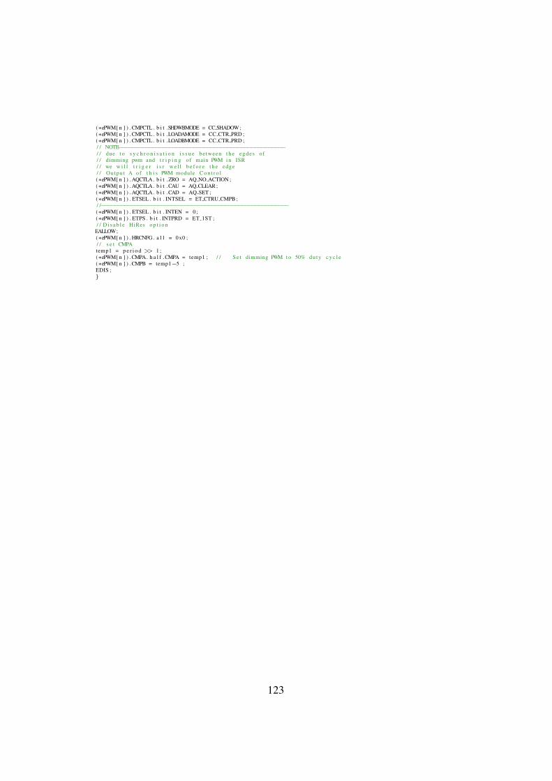
(∗ePWM[ n ] ) . CMPCTL. b i t .SHDWBMODE = CC SHADOW;(∗ePWM[ n ] ) . CMPCTL. b i t .LOADAMODE = CC CTR PRD ;(∗ePWM[ n ] ) . CMPCTL. b i t .LOADBMODE = CC CTR PRD ;/ / NOTE:−−−−−−−−−−−−−−−−−−−−−−−−−−−−−−−−−−−−−−−−−−−−−−−−−/ / due t o s y c h r o n i s a t i o n i s s u e between t h e egdes o f/ / dimming pwm and t r i p i n g of main PWM i n ISR/ / we w i l l t r i g e r i s r w e l l b e f o r e t h e edge/ / Outpu t A of t h i s PWM module C o n t r o l(∗ePWM[ n ] ) . AQCTLA. b i t .ZRO = AQ NO ACTION ;(∗ePWM[ n ] ) . AQCTLA. b i t .CAU = AQ CLEAR ;(∗ePWM[ n ] ) . AQCTLA. b i t .CAD = AQ SET ;(∗ePWM[ n ] ) . ETSEL . b i t . INTSEL = ET CTRU CMPB ;/ /−−−−−−−−−−−−−−−−−−−−−−−−−−−−−−−−−−−−−−−−−−−−−−−−−−−−−−−−(∗ePWM[ n ] ) . ETSEL . b i t . INTEN = 0 ;(∗ePWM[ n ] ) . ETPS . b i t . INTPRD = ET 1ST ;/ / D i s a b l e HiRes o p t i o n
EALLOW;(∗ePWM[ n ] ) . HRCNFG. a l l = 0x0 ;/ / s e t CMPAtemp1 = p e r i o d >> 1 ;(∗ePWM[ n ] ) . CMPA. h a l f .CMPA = temp1 ; / / S e t dimming PWM t o 50% du ty c y c l e(∗ePWM[ n ] ) . CMPB = temp1−5 ;EDIS ;}
123

Appendix C
Source Code for Open LoopMeasurement for Buck SMPS
C.1 CLA CodeModified CLA code is listed below
;====================================IIR2P2Z INIT .mac ro n;====================================; V a r i a b l e D e c l a r a t i o n s; The f o l l o w i n g a r e messages from t h e main CPU t o t h e CLA These a r e o b j e c t p o i n t e rCNTL 2P2Z Fdbk : n : . u s e c t ”CpuToCla1MsgRAM ” ,2 ; Feedback P o i n t e rCNTL 2P2Z Coef : n : . u s e c t ”CpuToCla1MsgRAM ” ,2 ; P o i n t e r t o f i l t e r C o e f f i c i e n t s
; P u b l i s h T e r m i n a l P o i n t e r s f o r a c c e s s from t h e C e n v i r o n m e n t ( o p t i o n a l ). d e f CNTL 2P2Z Fdbk : n :. d e f CNTL 2P2Z Coef : n :; s e t t e r m i n a l t o p o i n t t o ZeroNet
MOVL XAR2, #ZeroNetCLAMOVW DP , # CNTL 2P2Z Coef : n :MOVL @ CNTL 2P2Z Fdbk : n : , XAR2MOVL @ CNTL 2P2Z Coef : n : , XAR2.endm
;====================================IIR2P2Z .macro n;====================================
C o n t r o l L a w 2 P 2 Z S t a r t : n :
MMOV16 MAR0, @ CNTL 2P2Z Coef : n : ; MAR0 = p o i n t s t o C o e f i c i e n t s t r u c t u r eMMOV16 MAR1, @ CNTL 2P2Z Fdbk : n : ; MAR1 = p o i n t s t o f e e d b a c kMNOPMNOPMNOPMMOV32 MR0, ∗MAR0[#2]++ ; MR0 = s c a l i n gMUI16TOF32 MR1, ∗MAR1 ; MR1 = f e e d b a c k (ADC)MMPYF32 MR1,MR1,MR0 ; x = MR1( f e e d b a c k ) − MR0( Q v o l t s )MMOV32 MR0, ∗MAR0[#2]++ ; MR0 = s c a l i n gMADDF32 MR1,MR1,MR0MMOV32 MR3, ∗MAR0[#2]++ ; MR0 = Q v o l t sMSUBF32 MR1,MR1,MR3MUI16TOF32 MR3, @ EPwm: n : Regs.TBPRDMMINF32 MR1, #0 . 2 8 5 ; Lower L i m i tMMAXF32 MR1, #0 . 0 ; Upper L i m i t; / / / / / / / / / / / / / / / / / / / PWM Update S e c t i o n / / / / / / / / / / / / / / / / / / / / / / / / / / / / / / / / / / / / / /
MNOPMNOPMMPYF32 MR1, MR1, MR3MMPYF32 MR1,MR1,#65536 .0L ; As CMPA i s s h i f t e d by 16 b i t sMF32TOI32 MR1, MR1MMOV32 @ EPwm: n : Regs.CMPA.al l , MR1
124

Contro lLaw 2P2Z End : n :.endm
C.2 Modifications in Main CodeModification in main.c code is listed below
Thi s F i l e d e p i t c s changes from o r i g n a l s o u r c e code n e c s s a r y t o d e v e l o p an u n d e r s t s a n d
s t r u c t inputDS2P2Z {f l o a t s c a l i n g ; / / S c a l i n g f a c t o rf l o a t DC bias ; / / DC o p e r a t i n g p o i n tf l o a t Q v o l t s ;} ;
s t r u c t inputDS2P2Z Coef2P2Z 4 ;
Coef2P2Z 4 . s c a l i n g = 0 . 0 0 0 0 3 2 ; / / S c a l i n g F a c t o r i s found by i m p e r i c a l t e s t i n gCoef2P2Z 4 . Q v o l t s = 0 . 0 2 0 9 2 8 ; / / DC p o i n t i s chosen i n c o n t i n u e s c o n d u c t i o n modeCoef2P2Z 4 . DC bias = 0 . 0 ;
CNTL 2P2Z Fdbk4 = &AdcResu l t . ADCRESULT2; / / p o i n t t o Buck o u t p u t v o l t a g e v a l u eCNTL 2P2Z Coef4 = &Coef2P2Z 4 ; / / p o i n t t o f i r s t c o e f f o f Buck Loop
125