Evaluation of Cu Pillar Chemistries - Dow Chemical … of Cu Pillar Chemistries ... Max Center...
19
Dow.com Evaluation of Cu Pillar Chemistries iMAPS Device Packaging Conference – Spring 2016 Matthew Thorseth, Mark Scalisi, Inho Lee, Sang-Min Park, Yil-Hak Lee, Jonathan Prange, Masaaki Imanari, Mark Lefebvre, Jeff Calvert Presented at 2016 IMAPS Device Packaging
Transcript of Evaluation of Cu Pillar Chemistries - Dow Chemical … of Cu Pillar Chemistries ... Max Center...
Dow.com
Evaluation of Cu Pillar Chemistries iMAPS Device Packaging Conference – Spring 2016 Matthew Thorseth, Mark Scalisi, Inho Lee, Sang-Min Park, Yil-Hak Lee, Jonathan
Prange, Masaaki Imanari, Mark Lefebvre, Jeff Calvert
Presented at 2016 IMAPS
Device Packaging
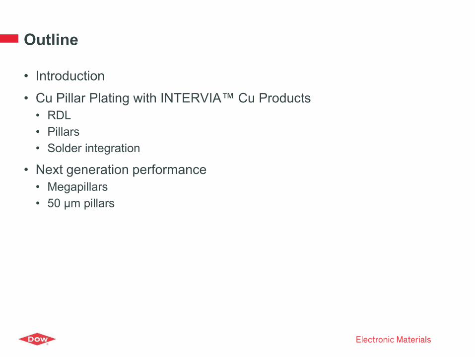
Outline
• Introduction
• Cu Pillar Plating with INTERVIA™ Cu Products
• RDL
• Pillars
• Solder integration
• Next generation performance
• Megapillars
• 50 μm pillars
Background and Introduction
3
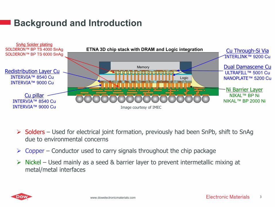
ETNA 3D chip stack with DRAM and Logic integration
Memory
Logic
SnAg C4 Bump SnAg Solder plating SOLDERON™ BP TS 4000 SnAg
SOLDERON™ BP TS 6000 SnAg
Redistribution Layer Cu INTERVIA™ 8540 Cu
INTERVIA™ 9000 Cu
Cu pillar INTERVIA™ 8540 Cu
INTERVIA™ 9000 Cu
Cu Through-Si Via INTERLINK™ 9200 Cu
Dual Damascene Cu ULTRAFILL™ 5001 Cu
NANOPLATE™ 5200 Cu
Ni Barrier Layer NIKAL™ BP Ni
NIKAL™ BP 2000 Ni
www.dowelectronicmaterials.com
Solders – Used for electrical joint formation, previously had been SnPb, shift to SnAg due to environmental concerns
Copper – Conductor used to carry signals throughout the chip package
Nickel – Used mainly as a seed & barrier layer to prevent intermetallic mixing at metal/metal interfaces
Image courtesy of IMEC
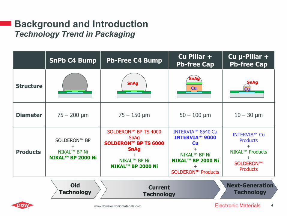
Background and Introduction Technology Trend in Packaging
SnPb C4 Bump Pb-Free C4 Bump Cu Pillar +
Pb-free Cap Cu µ-Pillar + Pb-free Cap
Structure
Diameter 75 – 200 µm 75 – 150 µm 50 – 100 µm 10 – 30 µm
Products
SOLDERON™ BP +
NIKAL™ BP Ni NIKAL™ BP 2000 Ni
SOLDERON™ BP TS 4000 SnAg
SOLDERON™ BP TS 6000 SnAg
+ NIKAL™ BP Ni
NIKAL™ BP 2000 Ni
INTERVIA™ 8540 Cu INTERVIA™ 9000
Cu +
NIKAL™ BP Ni NIKAL™ BP 2000 Ni
+ SOLDERON™ Products
INTERVIA™ Cu Products
+ NIKAL™ Products
+ SOLDERON™
Products
4 www.dowelectronicmaterials.com
Old Technology
Current Technology
Next-Generation Technology
SnAg SnAg
SnAg
Cu Cu
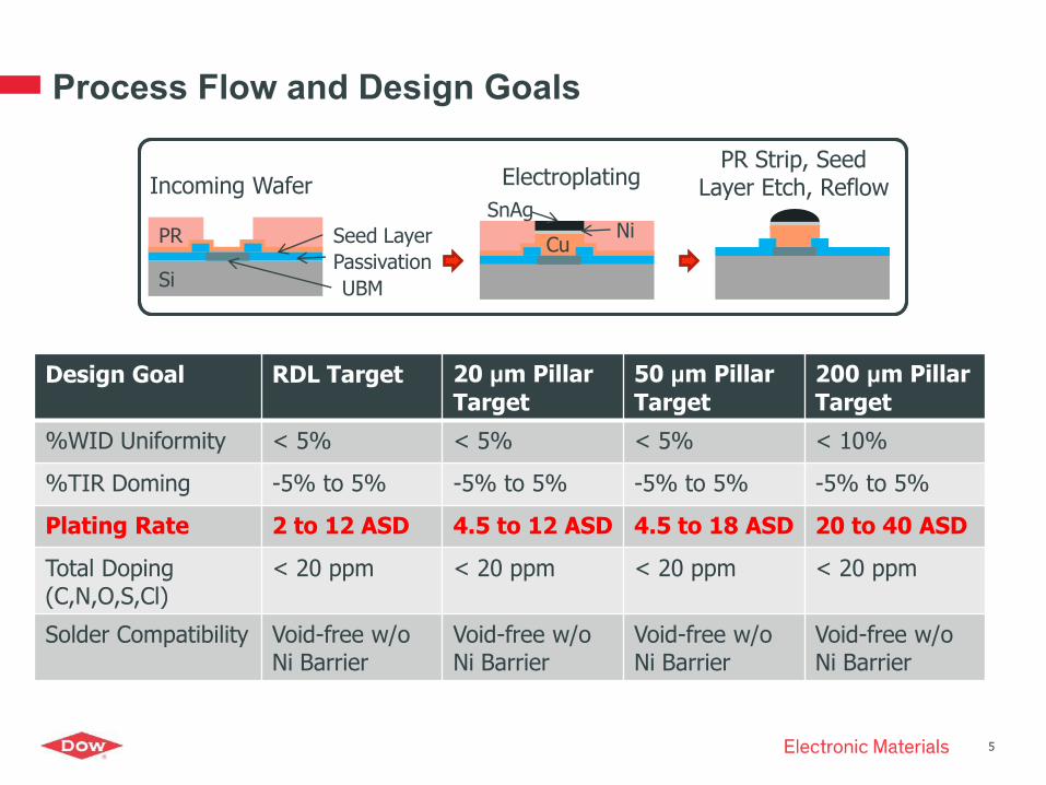
Process Flow and Design Goals
PR
Si Passivation
Seed Layer
UBM
Incoming Wafer Electroplating PR Strip, Seed
Layer Etch, Reflow
Cu Ni
SnAg
Design Goal RDL Target 20 μm Pillar
Target
50 μm Pillar
Target
200 μm Pillar
Target
%WID Uniformity < 5% < 5% < 5% < 10%
%TIR Doming -5% to 5% -5% to 5% -5% to 5% -5% to 5%
Plating Rate 2 to 12 ASD 4.5 to 12 ASD 4.5 to 18 ASD 20 to 40 ASD
Total Doping (C,N,O,S,Cl)
< 20 ppm < 20 ppm < 20 ppm < 20 ppm
Solder Compatibility Void-free w/o Ni Barrier
Void-free w/o Ni Barrier
Void-free w/o Ni Barrier
Void-free w/o Ni Barrier
5
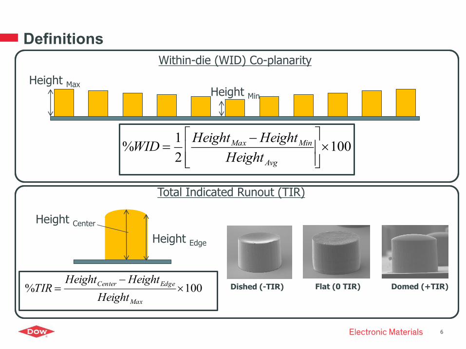
Definitions
1002
1%
Avg
MinMax
Height
HeightHeightWID
100%
Max
EdgeCenter
Height
HeightHeightTIR
Height Max Height Min
Within-die (WID) Co-planarity
Total Indicated Runout (TIR)
Height Center
Height Edge
Dished (-TIR) Flat (0 TIR) Domed (+TIR)
6
300 mm Data INTERVIA™ Copper Chemistry
INTERVIA™ 9000 Cu Images
Optical Image Profile
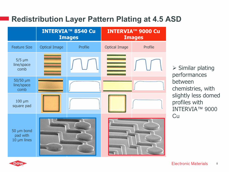
Redistribution Layer Pattern Plating at 4.5 ASD
IV8540 INTERVIA™ 8540 Cu
Images
Feature Size Optical Image Profile
5/5 μm line/space
comb
50/50 μm line/space
comb
100 μm square pad
50 μm bond pad with
10 μm lines
Similar plating performances between chemistries, with slightly less domed profiles with INTERVIA™ 9000
Cu
8
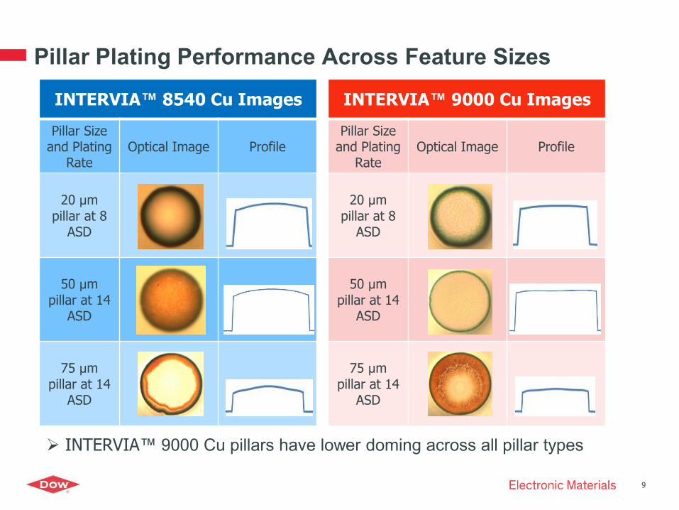
INTERVIA™ 8540 Cu Images
Pillar Size and Plating
Rate Optical Image Profile
20 μm pillar at 8
ASD
50 μm pillar at 14
ASD
75 μm pillar at 14
ASD
INTERVIA™ 9000 Cu Images
Pillar Size and Plating
Rate Optical Image Profile
20 μm pillar at 8
ASD
50 μm pillar at 14
ASD
75 μm pillar at 14
ASD
Pillar Plating Performance Across Feature Sizes
9
INTERVIA™ 9000 Cu pillars have lower doming across all pillar types
INTERVIA™ Cu 8540
Images
Current Density / ASD
Optical Image
Profile Dense Pitch
9
14
18
INTERVIA™ 8540 Cu vs. INTERVIA™ 9000 Cu 20 μm diameter micropillars
0%
5%
10%
15%
20%
8 9 12 14 16 18
%TI
R 4
0 μ
m P
itch
Current Density / ASD
INTERVIA 8540
INTERVIA 9000
0%
5%
10%
8 9 12 14 16 18
%W
ID 4
0 μ
m P
itch
Current Density / ASD
INTERVIA 8540
INTERVIA 9000
INTERVIA™ Cu 9000
Images
Current Density / ASD
Optical Image
Profile Dense Pitch
8
12
16
10
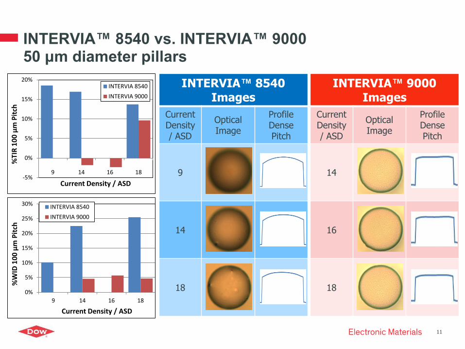
INTERVIA™ 8540
Images
Current Density / ASD
Optical Image
Profile Dense Pitch
9
14
18
INTERVIA™ 8540 vs. INTERVIA™ 9000 50 μm diameter pillars
INTERVIA™ 9000
Images
Current Density / ASD
Optical Image
Profile Dense Pitch
14
16
18
-5%
0%
5%
10%
15%
20%
9 14 16 18
%TI
R 1
00
μm
Pit
ch
Current Density / ASD
INTERVIA 8540
INTERVIA 9000
0%
5%
10%
15%
20%
25%
30%
9 14 16 18
%W
ID 1
00
μm
Pit
ch
Current Density / ASD
INTERVIA 8540
INTERVIA 9000
11
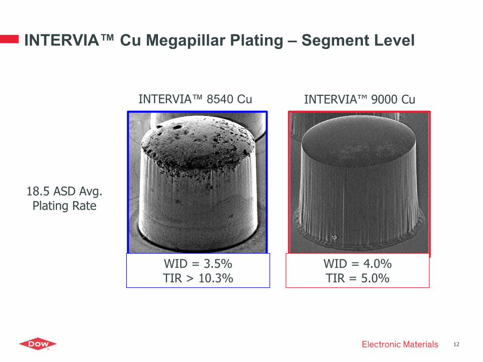
INTERVIA™ Cu Megapillar Plating – Segment Level
WID = 4.0% TIR = 5.0%
18.5 ASD Avg. Plating Rate
INTERVIA™ 9000 Cu INTERVIA™ 8540 Cu
WID = 3.5% TIR > 10.3%
12
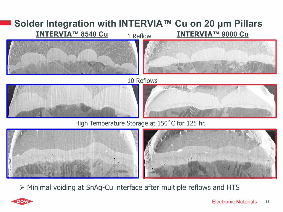
Solder Integration with INTERVIA™ Cu on 20 μm Pillars
High Temperature Storage at 150˚C for 125 hr.
1 Reflow
10 Reflows
INTERVIA™ 8540 Cu INTERVIA™ 9000 Cu
Minimal voiding at SnAg-Cu interface after multiple reflows and HTS
13
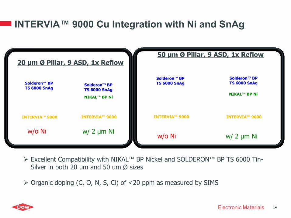
INTERVIA™ 9000 Cu Integration with Ni and SnAg
14
20 µm Ø Pillar, 9 ASD, 1x Reflow
w/o Ni w/ 2 µm Ni w/o Ni w/ 2 µm Ni
50 µm Ø Pillar, 9 ASD, 1x Reflow
Solderon™ BP TS 6000 SnAg
Solderon™ BP TS 6000 SnAg
Solderon™ BP TS 6000 SnAg
Solderon™ BP TS 6000 SnAg
INTERVIA™ 9000 INTERVIA™ 9000 INTERVIA™ 9000 INTERVIA™ 9000
NIKAL™ BP Ni NIKAL™ BP Ni
Excellent Compatibility with NIKAL™ BP Nickel and SOLDERON™ BP TS 6000 Tin-Silver in both 20 um and 50 um Ø sizes
Organic doping (C, O, N, S, Cl) of <20 ppm as measured by SIMS
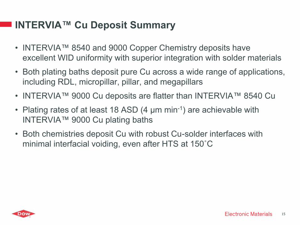
INTERVIA™ Cu Deposit Summary
• INTERVIA™ 8540 and 9000 Copper Chemistry deposits have
excellent WID uniformity with superior integration with solder materials
• Both plating baths deposit pure Cu across a wide range of applications,
including RDL, micropillar, pillar, and megapillars
• INTERVIA™ 9000 Cu deposits are flatter than INTERVIA™ 8540 Cu
• Plating rates of at least 18 ASD (4 μm min-1) are achievable with
INTERVIA™ 9000 Cu plating baths
• Both chemistries deposit Cu with robust Cu-solder interfaces with
minimal interfacial voiding, even after HTS at 150˚C
15
Next Generation Prototype Chemistries Segment Level Testing
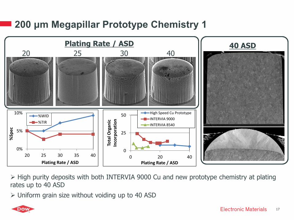
200 μm Megapillar Prototype Chemistry 1
17
High purity deposits with both INTERVIA 9000 Cu and new prototype chemistry at plating rates up to 40 ASD
Uniform grain size without voiding up to 40 ASD
0
25
50
0 20 40
Tota
l Org
anic
In
corp
ora
tio
n
Plating Rate / ASD
High Speed Cu Prototype
INTERVIA 9000
INTERVIA 8540
40 ASD Plating Rate / ASD
20 25 30 40
0%
5%
10%
20 25 30 35 40
%Sp
ec
Plating Rate / ASD
%WID
%TIR
Plating Rate / ASD
INTERVIA
9000 Cu Prototype Chemistry
14
20
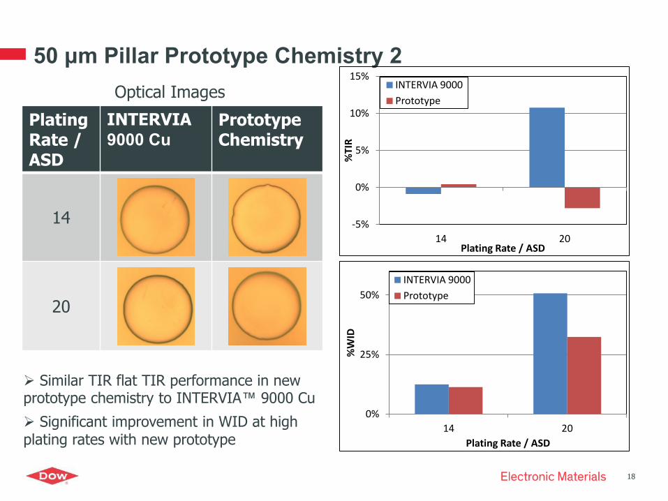
50 μm Pillar Prototype Chemistry 2
0%
25%
50%
14 20
%W
ID
Plating Rate / ASD
INTERVIA 9000
Prototype
-5%
0%
5%
10%
15%
14 20
%TI
R
Plating Rate / ASD
INTERVIA 9000
Prototype Optical Images
Similar TIR flat TIR performance in new prototype chemistry to INTERVIA™ 9000 Cu
Significant improvement in WID at high plating rates with new prototype
18
Thank You
®™ Trademark of the Dow Chemical Company (‘Dow’)
or an affiliated company of Dow