Evaluation Driver Board for AT-NPC 3-level 12in1 IGBT module · 2018-01-18 · Evaluation Driver...
26
© Fuji Electric Co., Ltd. All rights reserved. © Fuji Electric Co., Ltd. All rights reserved. PRELIMINARY AN-123 ver1.0 1 Evaluation Driver Board for AT-NPC 3-level 12in1 IGBT module Application Note December 2013 Device application Technology Dept. Semiconductor Sales Div. sales Group Fuji Electric co.,Ltd.
Transcript of Evaluation Driver Board for AT-NPC 3-level 12in1 IGBT module · 2018-01-18 · Evaluation Driver...
© Fuji Electric Co., Ltd. All rights reserved.© Fuji Electric Co., Ltd. All rights reserved.PRELIMINARY AN-123 ver1.0 1
Evaluation Driver Board forAT-NPC 3-level 12in1 IGBT module
Application Note
December 2013Device application Technology Dept.
Semiconductor Sales Div.sales Group
Fuji Electric co.,Ltd.
© Fuji Electric Co., Ltd. All rights reserved.© Fuji Electric Co., Ltd. All rights reserved.PRELIMINARY AN-123 ver1.0 22
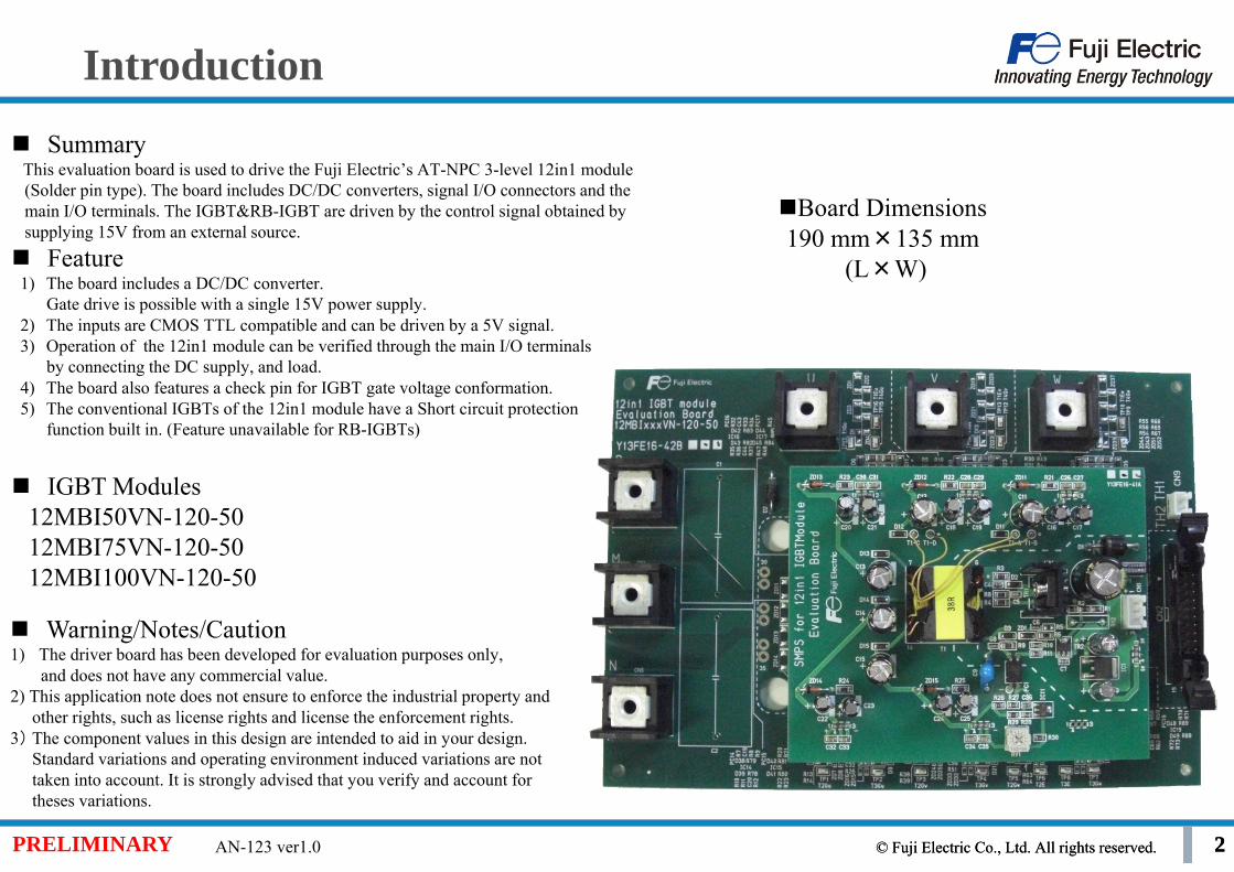
Introduction
SummaryThis evaluation board is used to drive the Fuji Electric’s AT-NPC 3-level 12in1 module(Solder pin type). The board includes DC/DC converters, signal I/O connectors and themain I/O terminals. The IGBT&RB-IGBT are driven by the control signal obtained by supplying 15V from an external source.
Feature1) The board includes a DC/DC converter.
Gate drive is possible with a single 15V power supply.2) The inputs are CMOS TTL compatible and can be driven by a 5V signal.3) Operation of the 12in1 module can be verified through the main I/O terminals
by connecting the DC supply, and load.4) The board also features a check pin for IGBT gate voltage conformation.5) The conventional IGBTs of the 12in1 module have a Short circuit protection
function built in. (Feature unavailable for RB-IGBTs)
Warning/Notes/Caution1) The driver board has been developed for evaluation purposes only,
and does not have any commercial value.2) This application note does not ensure to enforce the industrial property and
other rights, such as license rights and license the enforcement rights.3) The component values in this design are intended to aid in your design.
Standard variations and operating environment induced variations are nottaken into account. It is strongly advised that you verify and account for theses variations.
IGBT Modules12MBI50VN-120-5012MBI75VN-120-5012MBI100VN-120-50
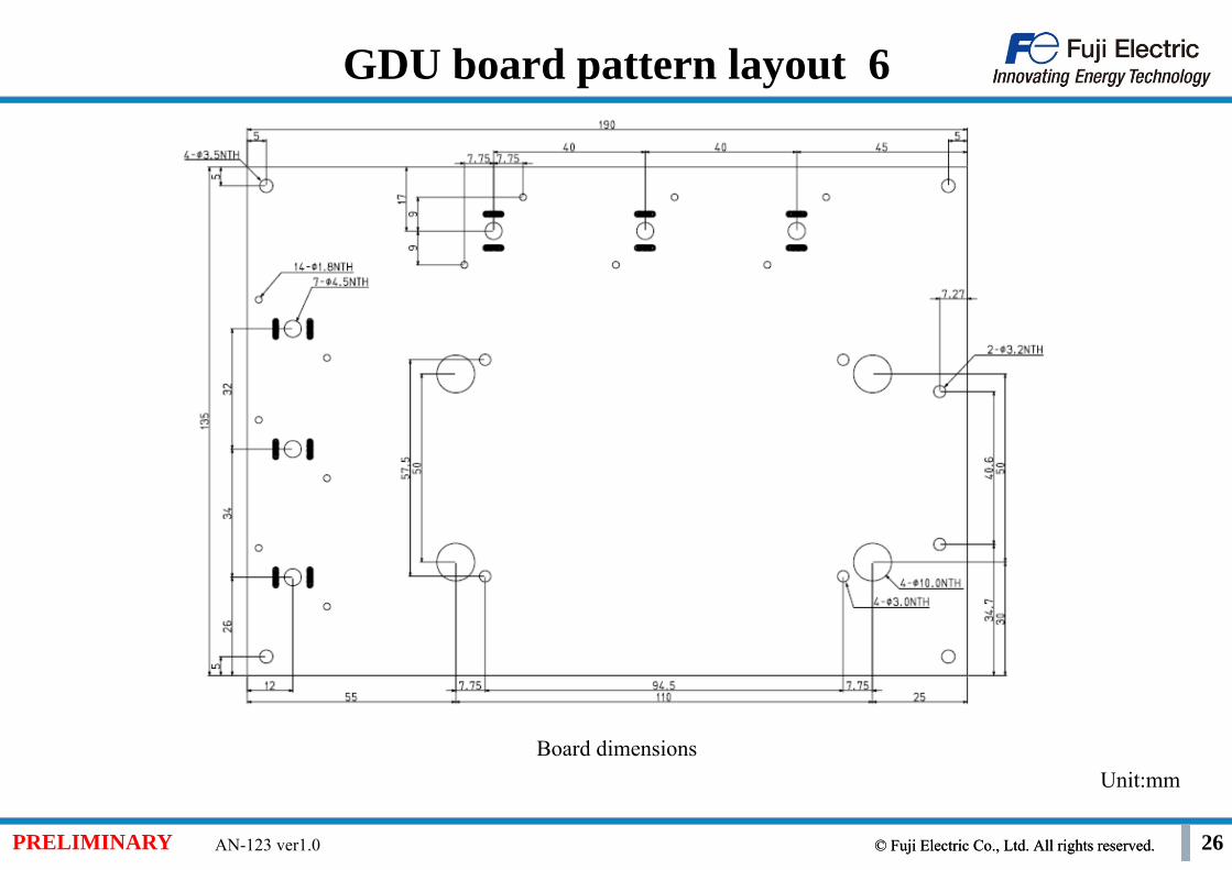
Board Dimensions190 mm×135 mm
(L×W)

© Fuji Electric Co., Ltd. All rights reserved.© Fuji Electric Co., Ltd. All rights reserved.PRELIMINARY AN-123 ver1.0 3
Electrical characteristics
Data sheet No.SN74HC04PW : sn74hc04.pdf (Texas Instruments Incorporated)ACPL-333J : AV02-1087EN+DS+ACPL-333J+25Oct2012.pdf (Avago Technologies)
Parameter Value Unit RemarksVDC(in) Primary DC/DC voltage supply range 10~18 V Recmended value 15VVout1 Output voltage from DC/DC converter +17/-10 V For IGBT drive supplyVout2 Primary side control voltage 5 V Non-isolationIout(DC) DC output current 0.15 A per 1 output. IGBT drive supplyIout(peak) Peak output current (t=1us) 10 A per 2 output. IGBT drive supply
VLogicIN PWM signals for High,low side IGBT and RB-IGBT 0/+5 V Follow the specification of SN74HC04PWVFAULT FAULT detection output 0/+5 V Follow the specification of ACPL-333JIFAULT FAULT detection output load current 8 mA Follow the specification of ACPL-333JVout IGBT drive voltage level for high,low side +15/-10 VIG MAX. peak output current ±2.5 A Follow the specification of ACPL-333JPout MAX. output power 1200 mW Follow the specification of ACPL-333Jfsw MAX PWM signal frequency 50 kHztPDELAY propagation delay time 200 nstPDISTO input to output propagation distortion 15 nsdmax MAX. duty cycle 100 %VCES(IGBT) MAX.collector-emitter voltage on IGBT 1200 VVCES(RB-IGBT) MAX.collector-emitter voltage on RB-IGBT 600 VTop operating temperature design target -10~50 degTstg Storage temperature design target -30~80 degNote:Other specifications follow specifications of SN74HC04PW and ACPL-333J
© Fuji Electric Co., Ltd. All rights reserved.© Fuji Electric Co., Ltd. All rights reserved.PRELIMINARY AN-123 ver1.0 4
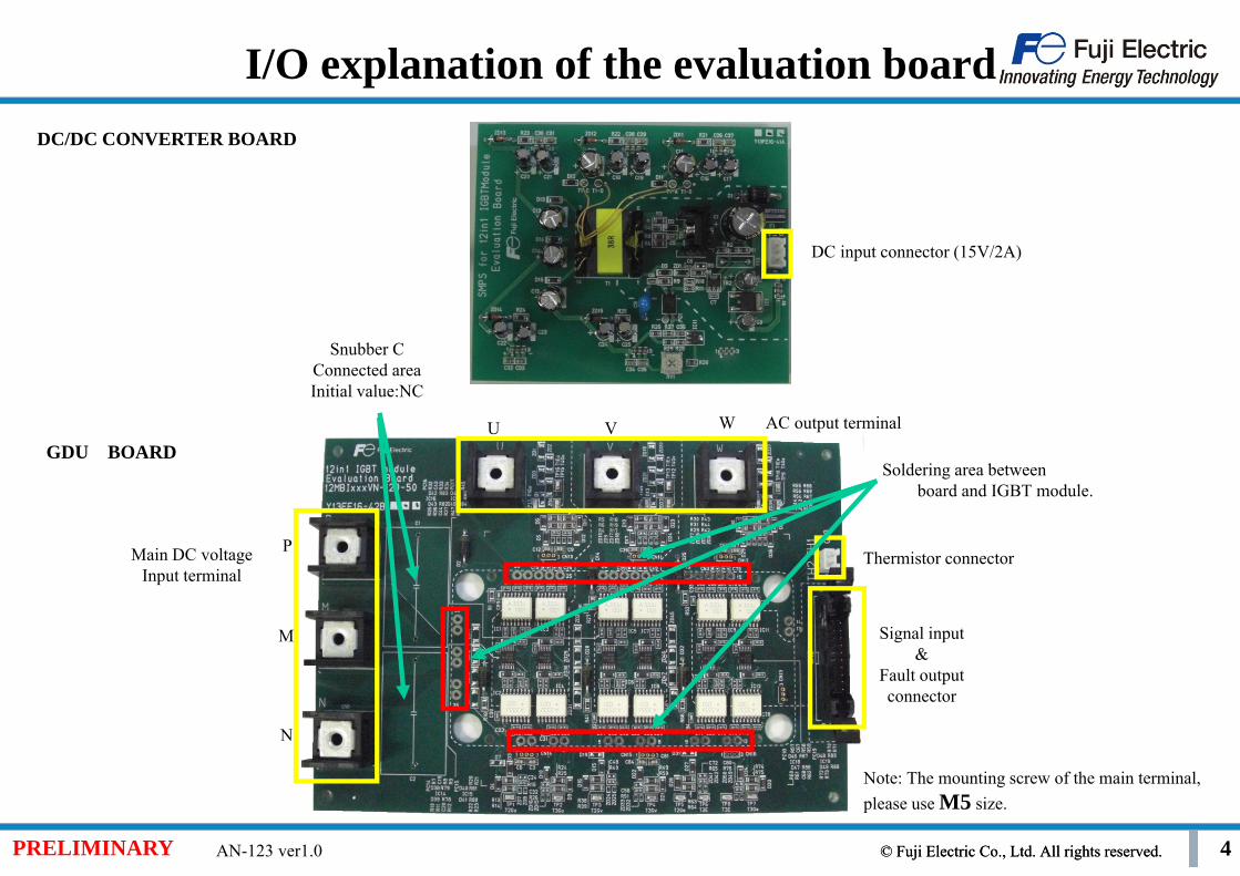
I/O explanation of the evaluation boardDC/DC CONVERTER BOARD
GDU BOARD
DC input connector (15V/2A)
Main DC voltageInput terminal
P
M
N
AC output terminal
Signal input&
Fault outputconnector
Thermistor connector
U V W
Snubber CConnected areaInitial value:NC
Note: The mounting screw of the main terminal, please use M5 size.
Soldering area between board and IGBT module.
© Fuji Electric Co., Ltd. All rights reserved.© Fuji Electric Co., Ltd. All rights reserved.PRELIMINARY AN-123 ver1.0 5
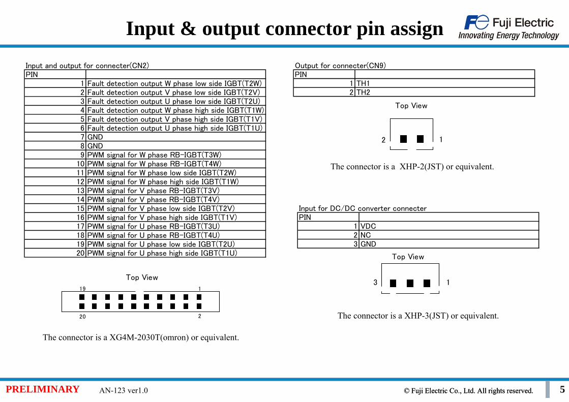
Input & output connector pin assignInput and output for connecter(CN2)PIN
1 Fault detection output W phase low side IGBT(T2W)2 Fault detection output V phase low side IGBT(T2V)3 Fault detection output U phase low side IGBT(T2U)4 Fault detection output W phase high side IGBT(T1W)5 Fault detection output V phase high side IGBT(T1V)6 Fault detection output U phase high side IGBT(T1U)7 GND8 GND9 PWM signal for W phase RB-IGBT(T3W)
10 PWM signal for W phase RB-IGBT(T4W)11 PWM signal for W phase low side IGBT(T2W)12 PWM signal for W phase high side IGBT(T1W)13 PWM signal for V phase RB-IGBT(T3V)14 PWM signal for V phase RB-IGBT(T4V)15 PWM signal for V phase low side IGBT(T2V)16 PWM signal for V phase high side IGBT(T1V)17 PWM signal for U phase RB-IGBT(T3U)18 PWM signal for U phase RB-IGBT(T4U)19 PWM signal for U phase low side IGBT(T2U)20 PWM signal for U phase high side IGBT(T1U)
1
2
19
20
Top View
Output for connecter(CN9)PIN
1 TH12 TH2
Top View
12
Input for DC/DC converter connecterPIN
1 VDC2 NC3 GND
Top View
13
The connector is a XG4M-2030T(omron) or equivalent.
The connector is a XHP-2(JST) or equivalent.
The connector is a XHP-3(JST) or equivalent.
© Fuji Electric Co., Ltd. All rights reserved.© Fuji Electric Co., Ltd. All rights reserved.PRELIMINARY AN-123 ver1.0 6
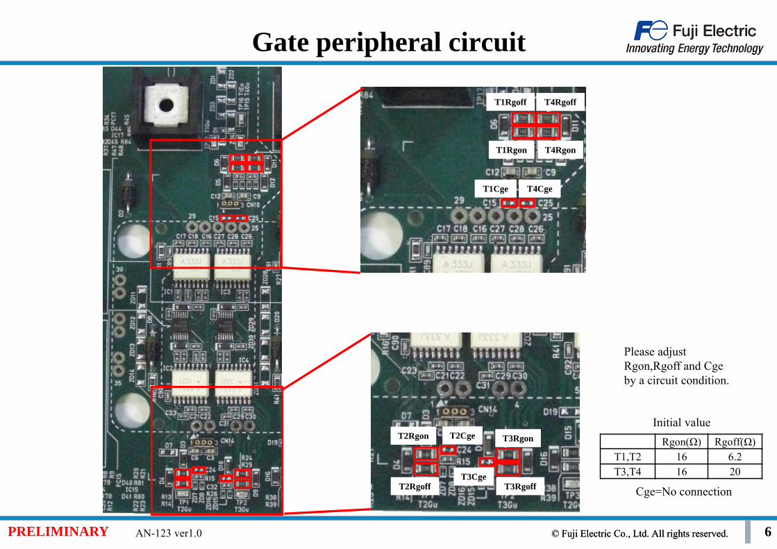
Gate peripheral circuit
T2Rgon
T2Rgoff
T2Cge
T3Cge
T3Rgon
T3Rgoff
T1Rgon
T1Cge
T1Rgoff
T4Cge
T4Rgon
T4Rgoff
Please adjust Rgon,Rgoff and Cgeby a circuit condition.
Rgon(Ω) Rgoff(Ω) T1,T2 16 6.2T3,T4 16 20
Cge=No connection
Initial value
© Fuji Electric Co., Ltd. All rights reserved.© Fuji Electric Co., Ltd. All rights reserved.PRELIMINARY AN-123 ver1.0 7
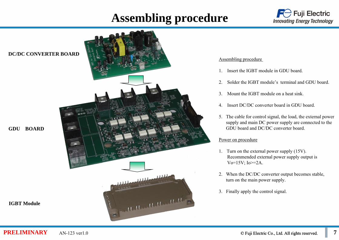
Assembling procedure
DC/DC CONVERTER BOARD
GDU BOARD
IGBT Module
Assembling procedure
1. Insert the IGBT module in GDU board.
2. Solder the IGBT module’s terminal and GDU board.
3. Mount the IGBT module on a heat sink.
4. Insert DC/DC converter board in GDU board.
5. The cable for control signal, the load, the external powersupply and main DC power supply are connected to theGDU board and DC/DC converter board.
Power on procedure
1. Turn on the external power supply (15V).Recommended external power supply output isVo=15V; Io>=2A.
2. When the DC/DC converter output becomes stable,turn on the main power supply.
3. Finally apply the control signal.
© Fuji Electric Co., Ltd. All rights reserved.© Fuji Electric Co., Ltd. All rights reserved.PRELIMINARY AN-123 ver1.0 8
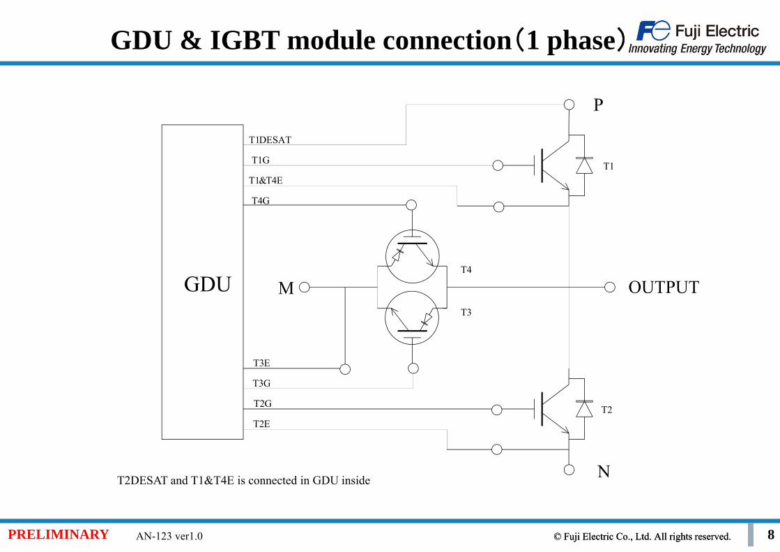
GDU & IGBT module connection(1 phase)
P
N
M OUTPUT
T2DESAT and T1&T4E is connected in GDU inside
T1
T2
T3
T4
GDU
T1G
T1&T4E
T4G
T1DESAT
T3E
T3G
T2E
T2G
© Fuji Electric Co., Ltd. All rights reserved.© Fuji Electric Co., Ltd. All rights reserved.PRELIMINARY AN-123 ver1.0 9
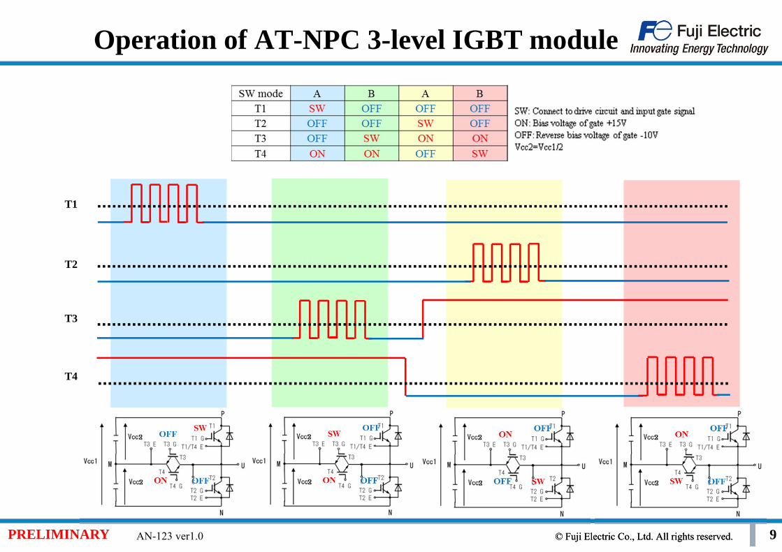
Operation of AT-NPC 3-level IGBT module
T1
T2
T3
T4
© Fuji Electric Co., Ltd. All rights reserved.© Fuji Electric Co., Ltd. All rights reserved.PRELIMINARY AN-123 ver1.0 10
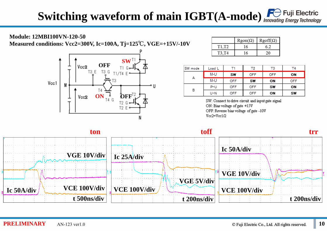
ON
SWOFF
OFF
Module: 12MBI100VN-120-50Measured conditions: Vcc2=300V, Ic=100A, Tj=125, VGE=+15V/-10V
ton toff trr
VCE 100V/divIc 50A/div
VGE 10V/div
t 500ns/divVCE 100V/div
Ic 25A/div
VGE 5V/div
t 200ns/divVCE 100V/div
Ic 50A/div
VGE 10V/div
t 200ns/div
Switching waveform of main IGBT(A-mode)
© Fuji Electric Co., Ltd. All rights reserved.© Fuji Electric Co., Ltd. All rights reserved.PRELIMINARY AN-123 ver1.0 11
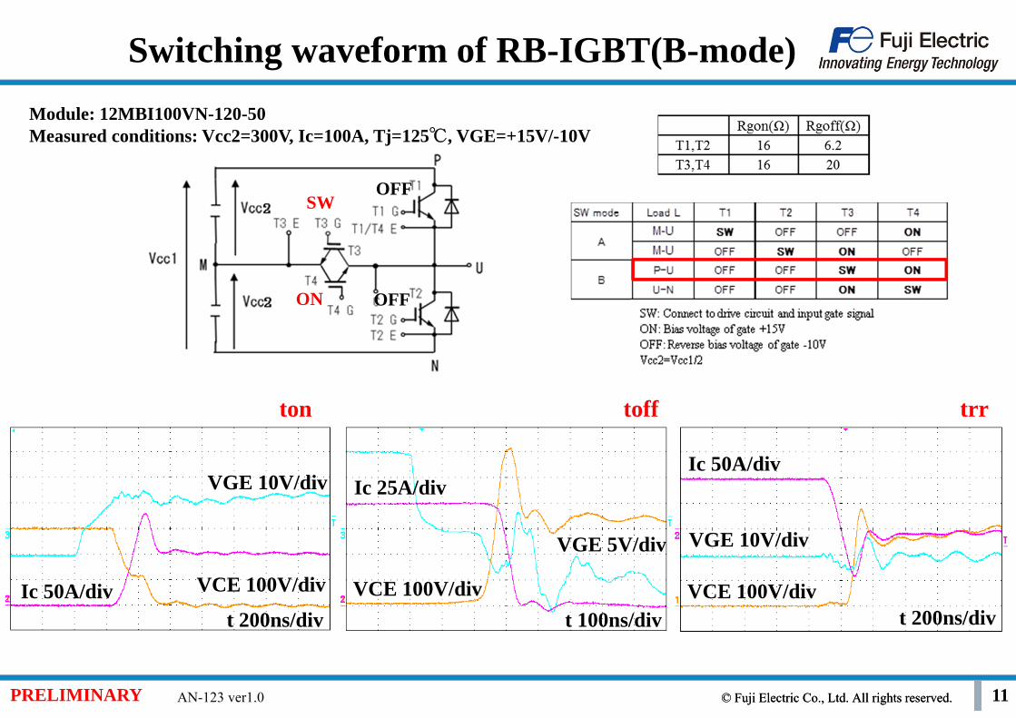
ON
OFFSW
OFF
ton toff trr
VCE 100V/divIc 50A/div
VGE 10V/div
t 200ns/divVCE 100V/div
Ic 25A/div
VGE 5V/div
t 100ns/divVCE 100V/div
Ic 50A/div
VGE 10V/div
t 200ns/div
Switching waveform of RB-IGBT(B-mode)Module: 12MBI100VN-120-50Measured conditions: Vcc2=300V, Ic=100A, Tj=125, VGE=+15V/-10V
© Fuji Electric Co., Ltd. All rights reserved.© Fuji Electric Co., Ltd. All rights reserved.PRELIMINARY AN-123 ver1.0 12
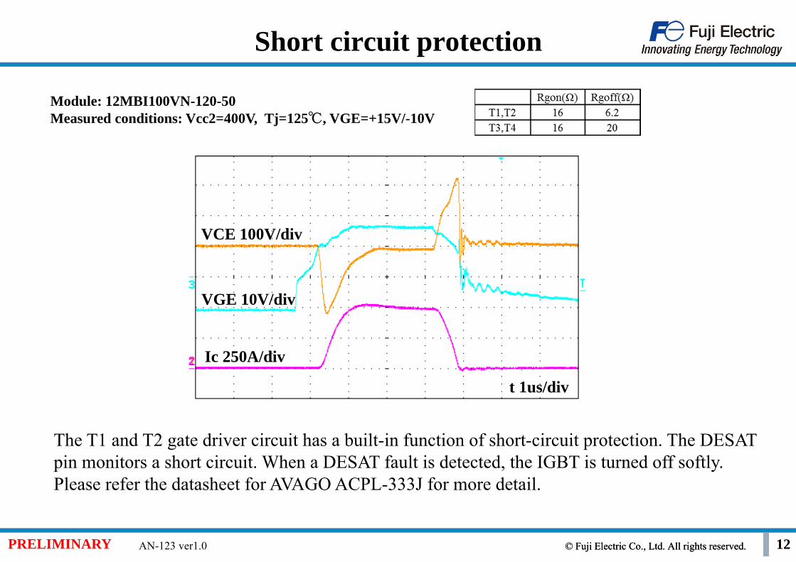
VCE 100V/div
Ic 250A/div
VGE 10V/div
t 1us/div
Module: 12MBI100VN-120-50Measured conditions: Vcc2=400V, Tj=125, VGE=+15V/-10V
Short circuit protection
The T1 and T2 gate driver circuit has a built-in function of short-circuit protection. The DESAT pin monitors a short circuit. When a DESAT fault is detected, the IGBT is turned off softly. Please refer the datasheet for AVAGO ACPL-333J for more detail.

© Fuji Electric Co., Ltd. All rights reserved.© Fuji Electric Co., Ltd. All rights reserved.PRELIMINARY AN-123 ver1.0 13
Before short circuit detection After short circuit detection
Output signal 10V/div
Input signal 5V/div
FAULT output 5V/div5V
5V
15V
Reset time of FAULT25usec.
t 5us/div
FAULT output
FAULT output, PWM input and IGBT gate-emitter voltage waveforms when a DESAT fault is detected are shown in the above figures.When the DESAT fault is detected, the IGBT is turned off and FAULT output switches from high to low.The driver automatically reset FAULT output after a fixed mute time of 25usec(typical). Please refer the datasheet for AVAGO ACPL-333J for more detail.
© Fuji Electric Co., Ltd. All rights reserved.© Fuji Electric Co., Ltd. All rights reserved.PRELIMINARY AN-123 ver1.0 14
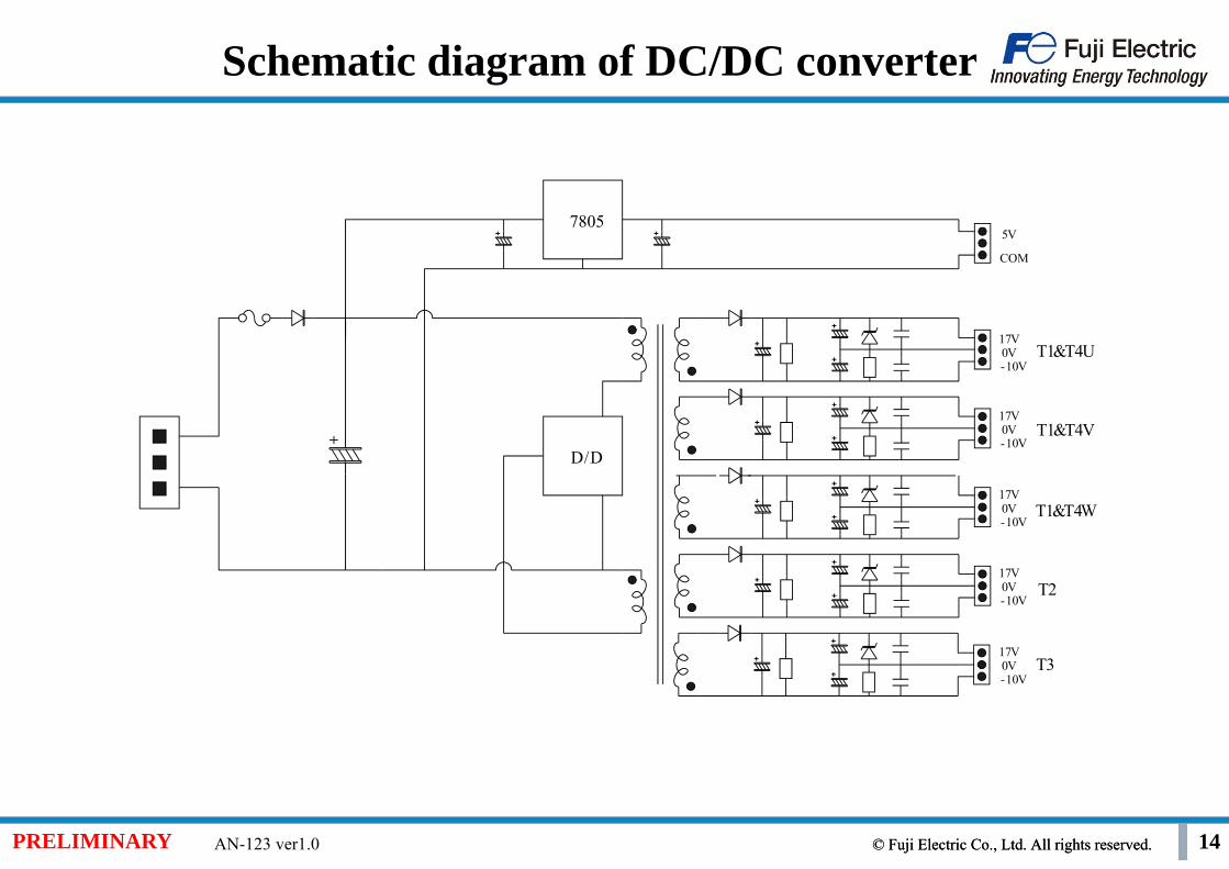
Schematic diagram of DC/DC converter
7805
D/D
5V
COM
17V0V-10V
17V0V-10V
17V0V-10V
17V0V-10V
17V0V-10V
T1&T4U
T1&T4V
T1&T4W
T2
T3
© Fuji Electric Co., Ltd. All rights reserved.© Fuji Electric Co., Ltd. All rights reserved.PRELIMINARY AN-123 ver1.0 15
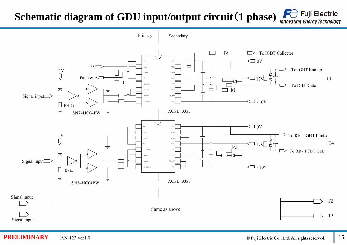
Schematic diagram of GDU input/output circuit(1 phase)
T1
T4
T2
T3
Signal input
Signal input
Vs
Vcc1
FAULT
Vs
CATHODE
VE
VLED
DESAT
VCC2
VEE
VOUT
VCLAMP
VEE
ANODE
ANODE
CATHODE
To IGBT Collector
0V
To IGBT Emitter
17V
- 10V
To IGBTGate
Vs
Vcc1
FAULT
Vs
CATHODE
VE
VLED
DESAT
VCC2
VEE
VOUT
VCLAMP
VEE
ANODE
ANODE
CATHODE
0V
To RB- IGBT Emitter
17V
- 10V
To RB- IGBT Gate
5V
Fault out
Signal input
5V
10kΩ
5V
10kΩ
Signal input
Primary Secondary
ACPL- 333JSN74HC04PW
ACPL- 333JSN74HC04PW
Same as above
© Fuji Electric Co., Ltd. All rights reserved.© Fuji Electric Co., Ltd. All rights reserved.PRELIMINARY AN-123 ver1.0 16
1A
1Y2A
3A
4A
5A
6A
2Y
3Y
4Y 5Y 6Y
GN
D
Vcc
1A
1Y2A
3A
4A
5A
6A
2Y
3Y
4Y 5Y 6Y
GN
D
Vcc
1A
1Y2A
3A
4A
5A
6A
2Y
3Y
4Y 5Y 6Y
GN
D
Vcc
1A
1Y2A
3A
4A
5A
6A
2Y
3Y
4Y 5Y 6Y
GN
D
Vcc
1A
1Y2A
3A
4A
5A
6A
2Y
3Y
4Y 5Y 6Y
GN
D
Vcc
1A
1Y2A
3A
4A
5A
6A
2Y
3Y
4Y 5Y 6Y
GN
D
Vcc
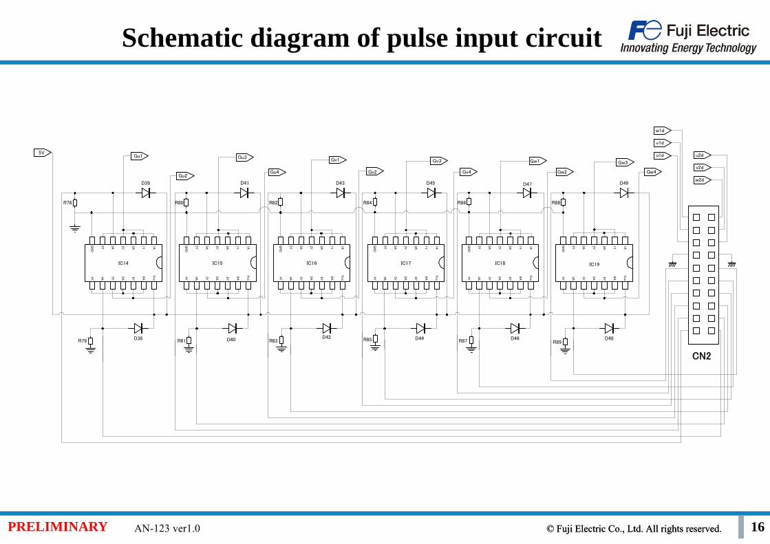
Gu1
Gu2
Gu3
Gu4
Gv1
Gv2
Gv3
Gv4
Gw1
Gw2
Gw3
Gw4
D39
D38
D41
D40 D42 D44 D46 D48
D43 D45 D47 D49
R78 R80 R82 R84 R86 R88
R89R87R85R83R81R79
IC14 IC15 IC16 IC17 IC18 IC19
CN2
u1d
v1d
w1d
v2d
u2d
w2d
5V
Schematic diagram of pulse input circuit
© Fuji Electric Co., Ltd. All rights reserved.© Fuji Electric Co., Ltd. All rights reserved.PRELIMINARY AN-123 ver1.0 17
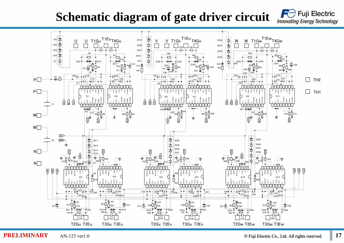
T2Gu T2Eu T2Gv T2Ev T2Gw T2EwT3Gu T3Eu T3Gv T3Ev T3Gw T3Ew
TH1
TH2
T1EwT4GwT1GwWW
T1EvT4GvT1GvVVT1EuT4GuT1GuUU
P
P
M
M
N
N
Vs
Vcc
1
FA
ULT
Vs
CA
TH
OD
E
VE
VLED
DESA
T
VC
C2
VEE
VO
UT
VC
LA
MP
VEE
AN
OD
E
AN
OD
E
CA
TH
OD
E
Vs
Vcc1
FA
ULT
Vs
CA
TH
OD
E
VE
VLED
DES
AT
VC
C2
VEE
VO
UT
VC
LA
MP
VEE
AN
OD
E
AN
OD
E
CA
TH
OD
E
Vs
Vcc
1
FA
ULT
Vs
CA
TH
OD
E
VE
VLED
DES
AT
VC
C2
VEE
VO
UT
VC
LA
MP
VEE
AN
OD
E
AN
OD
E
CA
TH
OD
E
Vs
Vcc
1
FA
ULT
Vs
CA
TH
OD
E
VE
VLED
DESA
T
VC
C2
VEE
VO
UT
VC
LA
MP
VEE
AN
OD
E
AN
OD
E
CA
TH
OD
E
Vs
Vcc
1
FA
ULT
Vs
CA
TH
OD
E
VE
VLED
DES
AT
VC
C2
VEE
VO
UT
VC
LA
MP
VEE
AN
OD
E
AN
OD
E
CA
TH
OD
E
Vs
Vcc
1
FA
ULT
Vs
CA
TH
OD
E
VE
VLED
DESA
T
VC
C2
VEE
VO
UT
VC
LA
MP
VEE
AN
OD
E
AN
OD
E
CA
TH
OD
E
Vs
Vcc1
FA
ULT
Vs
CA
TH
OD
E
VE
VLED
DES
AT
VC
C2
VEE
VO
UT
VC
LA
MP
VEE
AN
OD
E
AN
OD
E
CA
TH
OD
E
Vs
Vcc1
FA
ULT
Vs
CA
TH
OD
E
VE
VLED
DES
AT
VC
C2
VEE
VO
UT
VC
LA
MP
VEE
AN
OD
E
AN
OD
E
CA
TH
OD
E
Vs
Vcc1
FA
ULT
Vs
CA
TH
OD
E
VE
VLED
DES
AT
VC
C2
VEE
VO
UT
VC
LA
MP
VEE
AN
OD
E
AN
OD
E
CA
TH
OD
E
Vs
Vcc1
FA
ULT
Vs
CA
TH
OD
E
VE
VLED
DES
AT
VC
C2
VEE
VO
UT
VC
LA
MP
VEE
AN
OD
E
AN
OD
E
CA
TH
OD
E
Vs
Vcc1
FA
ULT
Vs
CA
TH
OD
E
VE
VLED
DES
AT
VC
C2
VEE
VO
UT
VC
LA
MP
VEE
AN
OD
E
AN
OD
E
CA
TH
OD
E
Vs
Vcc1
FA
ULT
Vs
CA
TH
OD
E
VE
VLED
DES
AT
VC
C2
VEE
VO
UT
VC
LA
MP
VEE
AN
OD
E
AN
OD
E
CA
TH
OD
E
ZD1
ZD2
ZD3
ZD4
ZD7 ZD8
ZD9 ZD10
ZD11
ZD12
ZD13
ZD14
ZD15 ZD16
ZD17
ZD18
ZD19
ZD20
ZD21
ZD22
ZD24 ZD25
ZD26 ZD27
ZD28
ZD29
ZD30
ZD31
ZD32 ZD33
ZD34
ZD35
ZD36
ZD37
ZD38
ZD39
ZD41 ZD42
ZD43 ZD44
ZD45
ZD46
ZD47
ZD48
ZD49 ZD50
ZD51
ZD52D1
D2
D3
D4
D5
D6
D7
D8
D9
D10
D11
D12
D13
D14
D15
D16
D17
D18
D19
D20
D21
D22
D23
D24
D25 D26
D27
D28
D29
D30
D31
D32
D33
D34
R1
R4
R5R6
R7R8 R9
R10 R11R12
R13R14
R15
R16
R17
R18 R19
R20 R21
R22R23
R24R25
R26
R27
R29
R30R31
R32
R33R34
R35R36
R38
R37
R39
R40
R41
R42
R43 R44
R45 R46
R47R48
R49R50
R51
R52
R54
R55R56
R57
R58 R59
R60R61
R62
R63 R64
R65
R66
R67
R68
R69
R70 R71
R72R73
R74 R75
R76
D35
D36
C1
C2
C15
C21C22
C23
C24
C16
C17
C18
C19
C20
C25
C26
C27 C28
C29
C30
C31
C32
C39
C40
C41
C42
C43
C44
C45 C46
C47
C48
C49
C50
C51 C52
C53 C54
C55
C56
C63
C64
C65
C66
C67
C68
C69 C70
C71
C72
C73
C74
C75C76
C77 C78
C79
C80
IC1
IC2
IC3
IC4
IC5
IC6
IC7
IC8
IC9
IC10
IC11
IC12
Gu1
u1d
5V
GND
Gu2
u2d
Gu3
Gv2
Gv3
Gw
2
Gw
3
Gw
4
Gw
1
Gv4
Gv1
Gu4 v1
d
w1d
w2d
v2d
P1
N1
P2
N2
P3
N3
P5
N5P4
N4
C89
C90
C91
C92
C93
C94
M1 M2
M3
M4
M5
Schematic diagram of gate driver circuit
© Fuji Electric Co., Ltd. All rights reserved.© Fuji Electric Co., Ltd. All rights reserved.PRELIMINARY AN-123 ver1.0 18
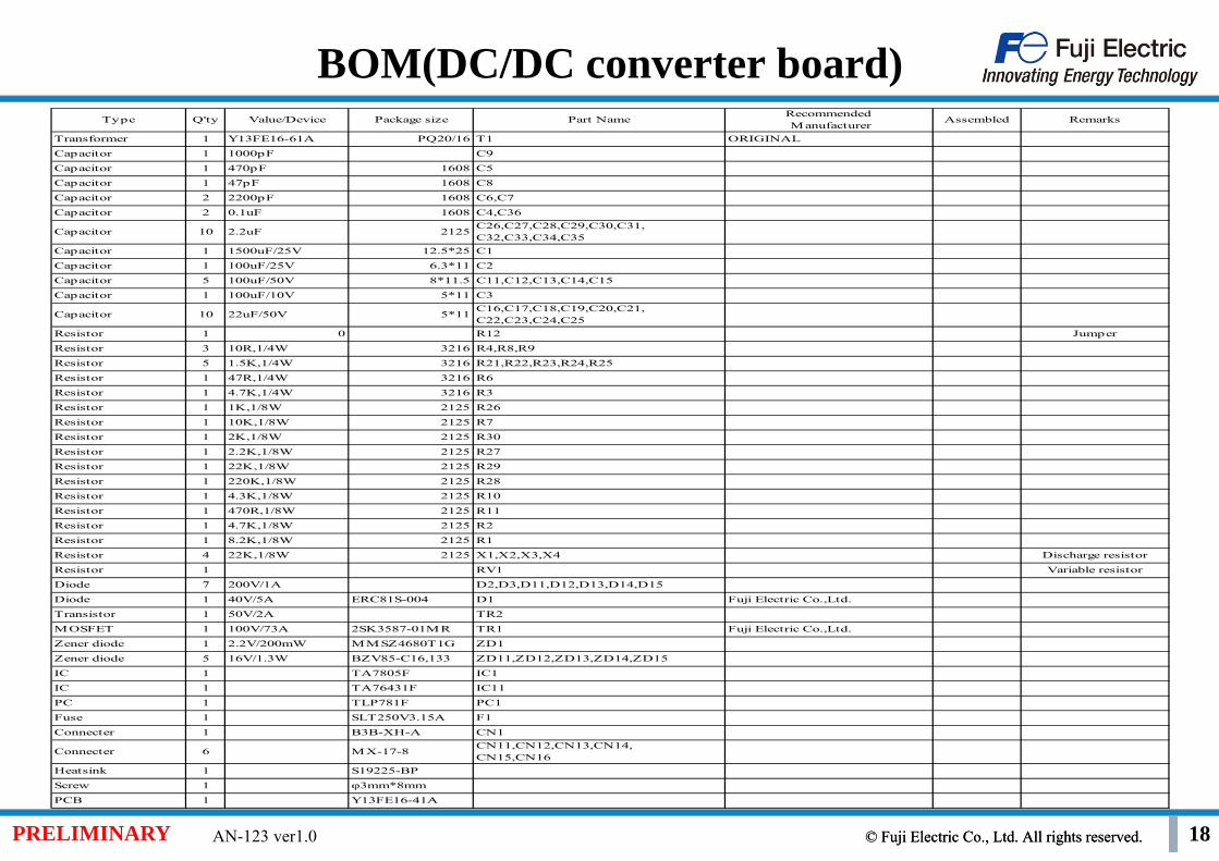
BOM(DC/DC converter board)Type Q'ty Value/Device Package size Part Name
Recommended Manufacturer
Assembled Remarks
Transformer 1 Y13FE16-61A PQ20/16 T1 ORIGINAL
Capacitor 1 1000pF C9
Capacitor 1 470pF 1608 C5
Capacitor 1 47pF 1608 C8
Capacitor 2 2200pF 1608 C6,C7
Capacitor 2 0.1uF 1608 C4,C36
Capacitor 10 2.2uF 2125C26,C27,C28,C29,C30,C31,C32,C33,C34,C35
Capacitor 1 1500uF/25V 12.5*25 C1
Capacitor 1 100uF/25V 6.3*11 C2
Capacitor 5 100uF/50V 8*11.5 C11,C12,C13,C14,C15
Capacitor 1 100uF/10V 5*11 C3
Capacitor 10 22uF/50V 5*11C16,C17,C18,C19,C20,C21,C22,C23,C24,C25
Resistor 1 0 R12 Jumper
Resistor 3 10R,1/4W 3216 R4,R8,R9
Resistor 5 1.5K,1/4W 3216 R21,R22,R23,R24,R25
Resistor 1 47R,1/4W 3216 R6
Resistor 1 4.7K,1/4W 3216 R3
Resistor 1 1K,1/8W 2125 R26
Resistor 1 10K,1/8W 2125 R7
Resistor 1 2K,1/8W 2125 R30
Resistor 1 2.2K,1/8W 2125 R27
Resistor 1 22K,1/8W 2125 R29
Resistor 1 220K,1/8W 2125 R28
Resistor 1 4.3K,1/8W 2125 R10
Resistor 1 470R,1/8W 2125 R11
Resistor 1 4.7K,1/8W 2125 R2
Resistor 1 8.2K,1/8W 2125 R1
Resistor 4 22K,1/8W 2125 X1,X2,X3,X4 Discharge resistor
Resistor 1 RV1 Variable resistor
Diode 7 200V/1A D2,D3,D11,D12,D13,D14,D15
Diode 1 40V/5A ERC81S-004 D1 Fuji Electric Co.,Ltd.
Transistor 1 50V/2A TR2
MOSFET 1 100V/73A 2SK3587-01MR TR1 Fuji Electric Co.,Ltd.
Zener diode 1 2.2V/200mW MMSZ4680T1G ZD1
Zener diode 5 16V/1.3W BZV85-C16,133 ZD11,ZD12,ZD13,ZD14,ZD15
IC 1 TA7805F IC1
IC 1 TA76431F IC11
PC 1 TLP781F PC1
Fuse 1 SLT250V3.15A F1
Connecter 1 B3B-XH-A CN1
Connecter 6 MX-17-8CN11,CN12,CN13,CN14,CN15,CN16
Heatsink 1 S19225-BP
Screw 1 φ3mm*8mm
PCB 1 Y13FE16-41A
© Fuji Electric Co., Ltd. All rights reserved.© Fuji Electric Co., Ltd. All rights reserved.PRELIMINARY AN-123 ver1.0 19
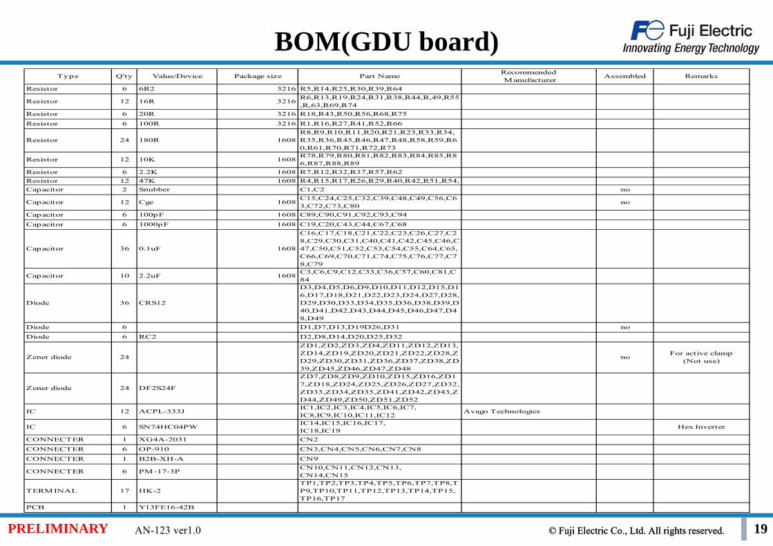
BOM(GDU board)Type Q'ty Value/Device Package size Part Name
Recommended Manufacturer
Assembled Remarks
Resistor 6 6R2 3216 R5,R14,R25,R30,R39,R64
Resistor 12 16R 3216R6,R13,R19,R24,R31,R38,R44,R,49,R55,R,63,R69,R74
Resistor 6 20R 3216 R18,R43,R50,R56,R68,R75
Resistor 6 100R 3216 R1,R16,R27,R41,R52,R66
Resistor 24 180R 1608R8,R9,R10,R11,R20,R21,R23,R33,R34,R35,R36,R45,R46,R47,R48,R58,R59,R60,R61,R70,R71,R72,R73
Resistor 12 10K 1608R78,R79,R80,R81,R82,R83,R84,R85,R86,R87,R88,R89
Resistor 6 2.2K 1608 R7,R12,R32,R37,R57,R62Resistor 12 47K 1608 R4,R15,R17,R26,R29,R40,R42,R51,R54,Capacitor 2 Snubber C1,C2 no
Capacitor 12 Cge 1608C15,C24,C25,C32,C39,C48,C49,C56,C63,C72,C73,C80
no
Capacitor 6 100pF 1608 C89,C90,C91,C92,C93,C94
Capacitor 6 1000pF 1608 C19,C20,C43,C44,C67,C68
Capacitor 36 0.1uF 1608
C16,C17,C18,C21,C22,C23,C26,C27,C28,C29,C30,C31,C40,C41,C42,C45,C46,C47,C50,C51,C52,C53,C54,C55,C64,C65,C66,C69,C70,C71,C74,C75,C76,C77,C78,C79
Capacitor 10 2.2uF 1608C3,C6,C9,C12,C33,C36,C57,C60,C81,C84
Diode 36 CRS12
D3,D4,D5,D6,D9,D10,D11,D12,D15,D16,D17,D18,D21,D22,D23,D24,D27,D28,D29,D30,D33,D34,D35,D36,D38,D39,D40,D41,D42,D43,D44,D45,D46,D47,D48,D49
Diode 6 D1,D7,D13,D19D26,D31 no
Diode 6 RC2 D2,D8,D14,D20,D25,D32
Zener diode 24
ZD1,ZD2,ZD3,ZD4,ZD11,ZD12,ZD13,ZD14,ZD19,ZD20,ZD21,ZD22,ZD28,ZD29,ZD30,ZD31,ZD36,ZD37,ZD38,ZD39,ZD45,ZD46,ZD47,ZD48
noFor active clamp
(Not use)
Zener diode 24 DF2S24F
ZD7,ZD8,ZD9,ZD10,ZD15,ZD16,ZD17,ZD18,ZD24,ZD25,ZD26,ZD27,ZD32,ZD33,ZD34,ZD35,ZD41,ZD42,ZD43,ZD44,ZD49,ZD50,ZD51,ZD52
IC 12 ACPL-333JIC1,IC2,IC3,IC4,IC5,IC6,IC7,IC8,IC9,IC10,IC11,IC12
Avago Technologies
IC 6 SN74HC04PWIC14,IC15,IC16,IC17,IC18,IC19
Hex Inverter
CONNECTER 1 XG4A-2031 CN2
CONNECTER 6 OP-910 CN3,CN4,CN5,CN6,CN7,CN8
CONNECTER 1 B2B-XH-A CN9
CONNECTER 6 PM-17-3PCN10,CN11,CN12,CN13,CN14,CN15
TERMINAL 17 HK-2TP1,TP2,TP3,TP4,TP5,TP6,TP7,TP8,TP9,TP10,TP11,TP12,TP13,TP14,TP15,TP16,TP17
PCB 1 Y13FE16-42B
© Fuji Electric Co., Ltd. All rights reserved.© Fuji Electric Co., Ltd. All rights reserved.PRELIMINARY AN-123 ver1.0 20
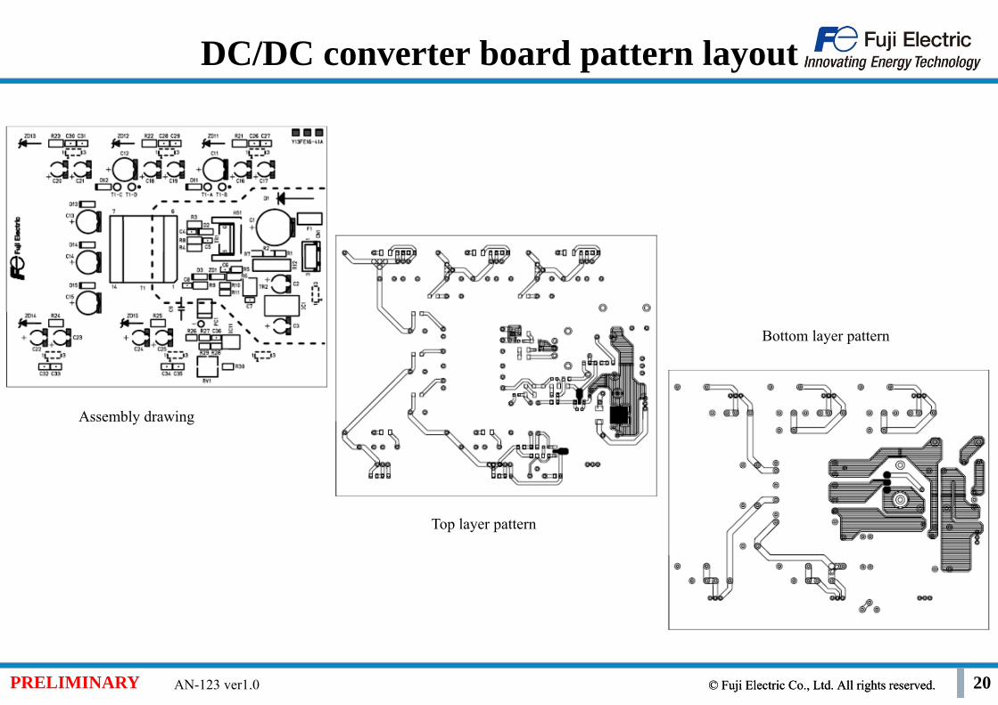
DC/DC converter board pattern layout
Assembly drawing
Top layer pattern
Bottom layer pattern
© Fuji Electric Co., Ltd. All rights reserved.© Fuji Electric Co., Ltd. All rights reserved.PRELIMINARY AN-123 ver1.0 21
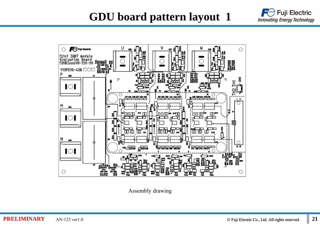
GDU board pattern layout 1
Assembly drawing
© Fuji Electric Co., Ltd. All rights reserved.© Fuji Electric Co., Ltd. All rights reserved.PRELIMINARY AN-123 ver1.0 22
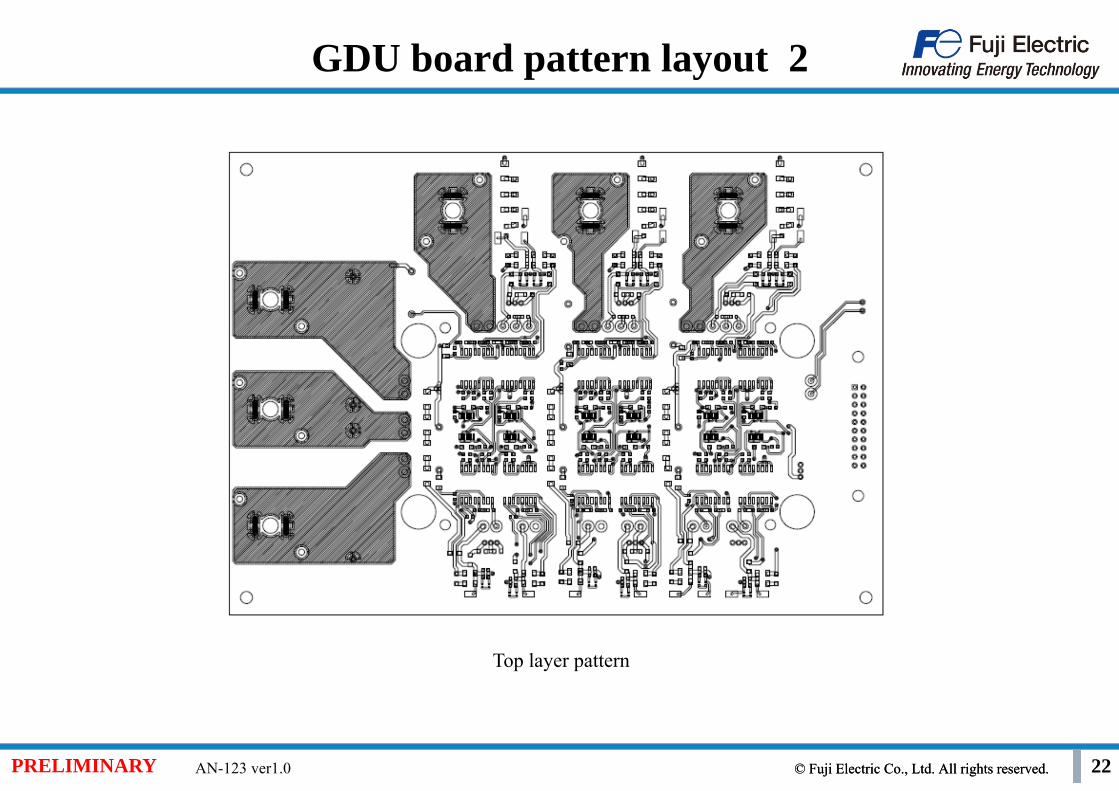
GDU board pattern layout 2
Top layer pattern
© Fuji Electric Co., Ltd. All rights reserved.© Fuji Electric Co., Ltd. All rights reserved.PRELIMINARY AN-123 ver1.0 23
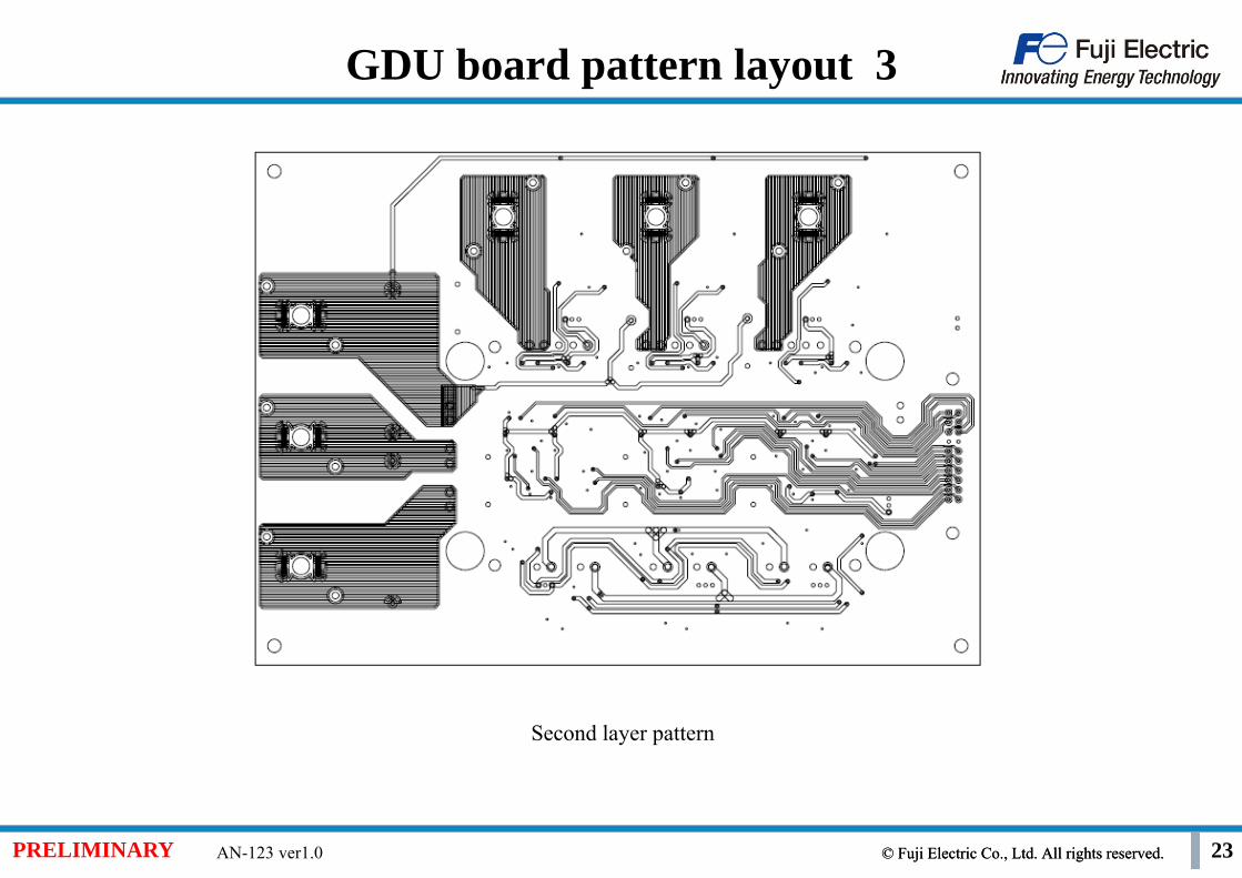
GDU board pattern layout 3
Second layer pattern
© Fuji Electric Co., Ltd. All rights reserved.© Fuji Electric Co., Ltd. All rights reserved.PRELIMINARY AN-123 ver1.0 24
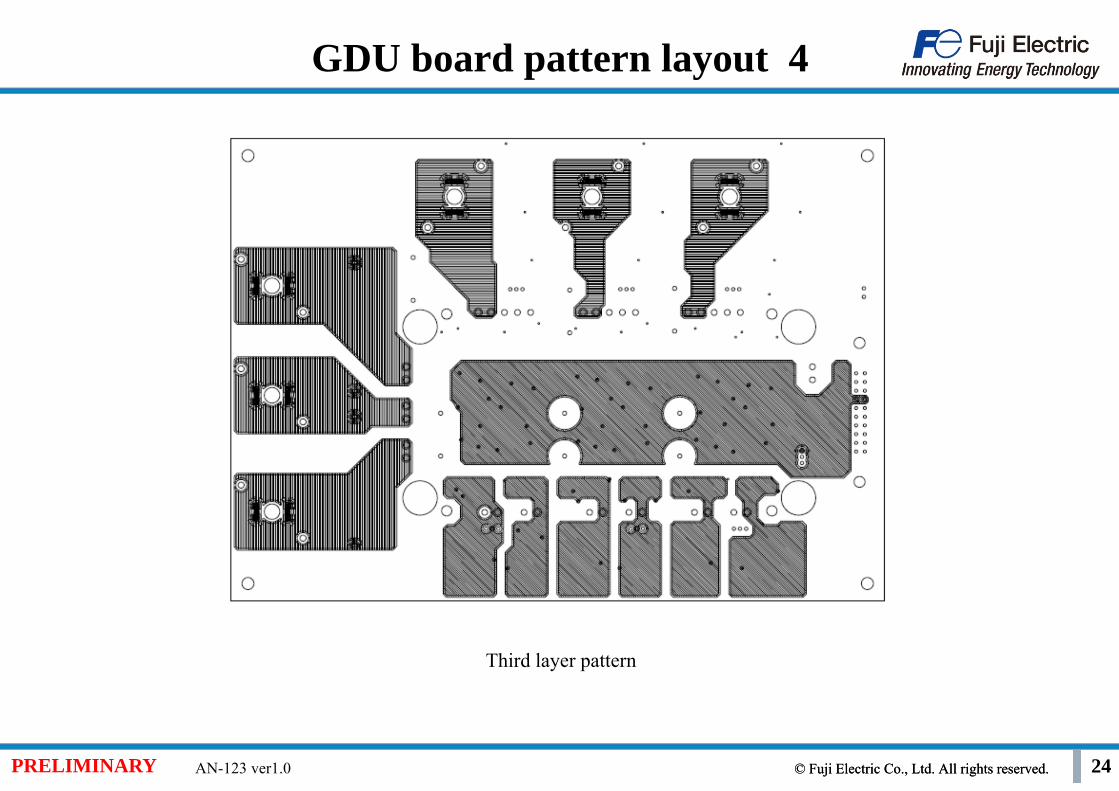
GDU board pattern layout 4
Third layer pattern
© Fuji Electric Co., Ltd. All rights reserved.© Fuji Electric Co., Ltd. All rights reserved.PRELIMINARY AN-123 ver1.0 25
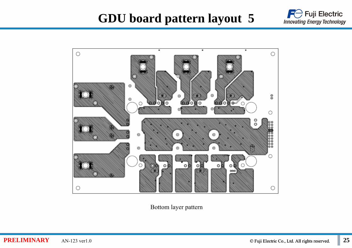
GDU board pattern layout 5
Bottom layer pattern
© Fuji Electric Co., Ltd. All rights reserved.© Fuji Electric Co., Ltd. All rights reserved.PRELIMINARY AN-123 ver1.0 26
GDU board pattern layout 6
Board dimensionsUnit:mm