OTSG/MEDCOM Medical Evaluation Board (MEB)/ Physical Evaluation Board (PEB) Overview Brief.

Fujitsu ASSP Product
1/24Power Management
MB39A112 Evaluation Board Rev1.0E
Rev 1.0EApril,2003
Evaluation board ManualEvaluation board Manual
MB39A112MB39A112

Fujitsu ASSP Product
2/24Power Management
MB39A112 Evaluation Board Rev1.0E
1. 1. Evaluation Board SpecificationsEvaluation Board SpecificationsThe MB39A112 evaluation board is a surface mounting circuit board of the down conversion circuit of 3ch.1.2V, 3.3V, and 5V are output from the output terminal in three forms, and the current of 1.5A or less is supplied.Moreover, FET is turned off when the under voltage lockout protection circuit do operation or the short-circuit protection is detected by the protection function, and the output is stopped.In addition, the on/off control and the soft-start of each channel can be set.
2. 2. Evaluation Board SpecificationsEvaluation Board SpecificationsTerminal MIN TYP MAX Unit
VIN 7 12 20 V2115 2350 2585 kHz
CH1 VO1 1.14 1.2 1.26 VCH2 VO2 3.13 3.3 3.47 VCH3 VO3 4.75 5 5.25 VCH1 VO1 6 12 24 mVCH2 VO2 16 33 64 mVCH3 VO3 25 50 100 mVCH1 VO1 800 1200 1500 mACH2 VO2 150 500 1000 mACH3 VO3 150 200 300 mACH1 - 6.3 10 18.6 msCH2 - 7.8 12 22.8 msCH3 - 7.8 12 22.8 ms
- 430 720 1420 µs
ItemInput voltage
Oscillation frequency
Short-circuit detection time
Output voltage
Ripple voltage
Output current
Soft-start time
Fujitsu ASSP Product
3/24Power Management
MB39A112 Evaluation Board Rev1.0E
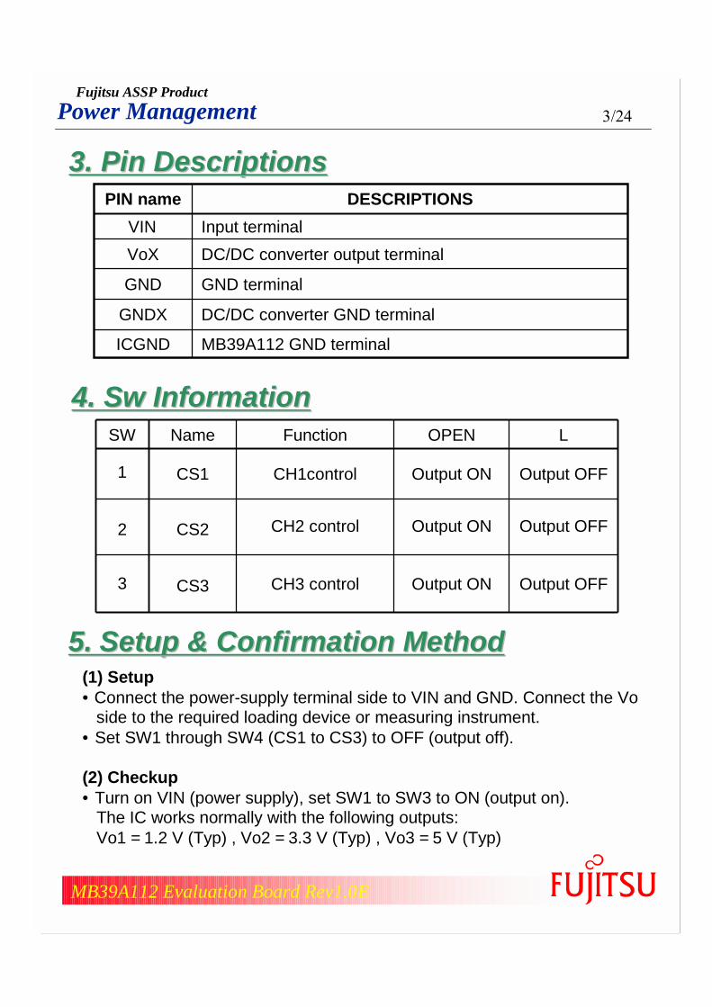
3. 3. Pin DescriptionsPin Descriptions
MB39A112 GND terminalICGND
GND terminalGND
DC/DC converter output terminalVoXInput terminalVIN
DESCRIPTIONSPIN name
DC/DC converter GND terminalGNDX
4. 4. SwSw InformationInformation
Output OFF
L
Output ON
OPEN
CH1control
Function
CS22
CS11
NameSW
CS33
CH2 control
CH3 control
Output ON
Output ON
Output OFF
Output OFF
(1) Setup• Connect the power-supply terminal side to VIN and GND. Connect the Vo
side to the required loading device or measuring instrument.• Set SW1 through SW4 (CS1 to CS3) to OFF (output off).
(2) Checkup• Turn on VIN (power supply), set SW1 to SW3 to ON (output on).
The IC works normally with the following outputs:Vo1 = 1.2 V (Typ) , Vo2 = 3.3 V (Typ) , Vo3 = 5 V (Typ)
5.5. Setup & Confirmation MethodSetup & Confirmation Method
Fujitsu ASSP Product
4/24Power Management
MB39A112 Evaluation Board Rev1.0E
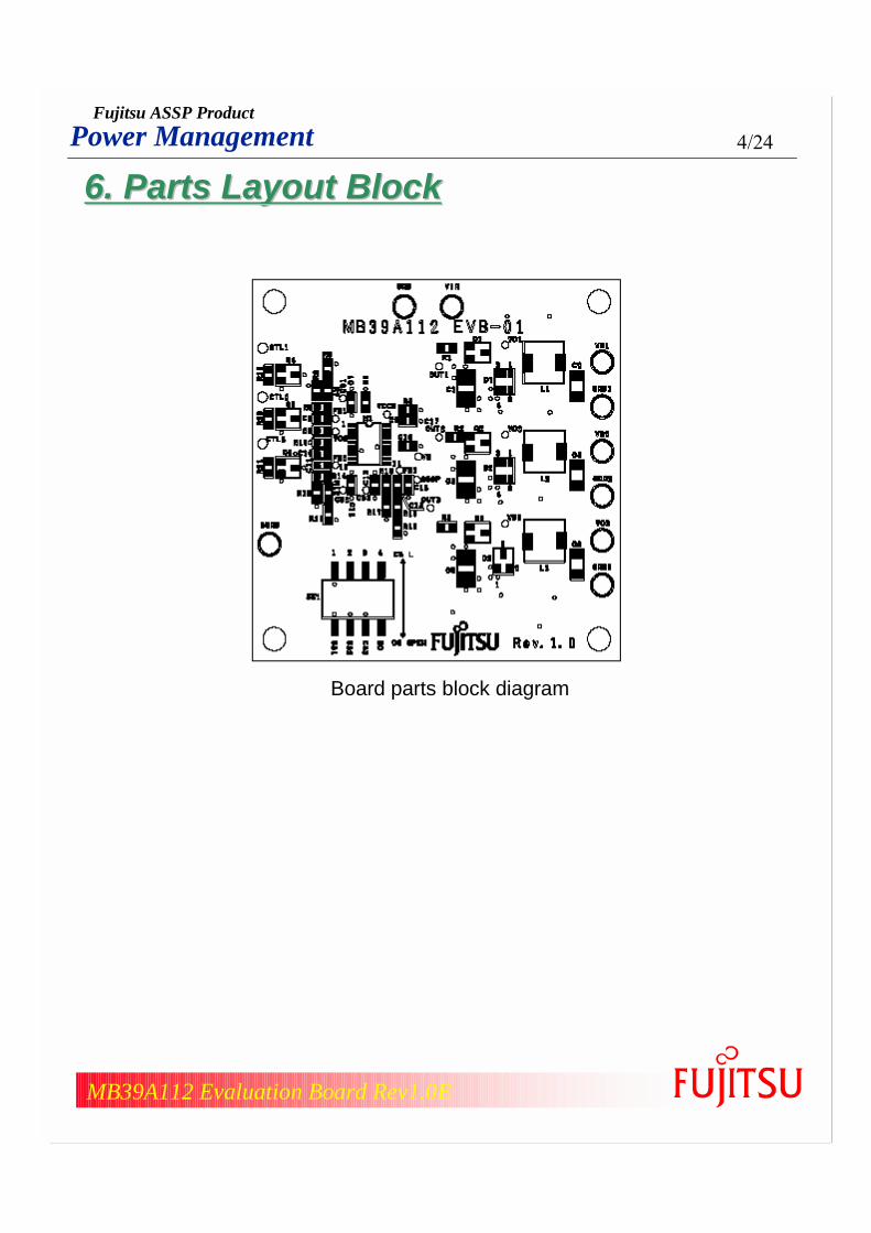
6. 6. Parts Layout BlockParts Layout Block
Board parts block diagram

Fujitsu ASSP Product
5/24Power Management
MB39A112 Evaluation Board Rev1.0E
Board Layout
Top Side
Bottom Side
Inside GND(Layer 2)
Inside VIN(Layer 3)

Fujitsu ASSP Product
6/24Power Management
MB39A112 Evaluation Board Rev1.0E
7. 7. Circuit DiagramCircuit Diagram
-INE2
OUT2
Vo2(3.3V)Io2=0.15A to 1A
VIN(12V)
OSC
2.5V
2.0V
SCP
PowerON/OFF
CTLVR
ErrorAmp reference1.0V/1.23V
VREF
VCC
bias 3.5V
GND
ErrorAmp power supplySCPComp. power supplyCharge current
1µA
9B
10
8
CS2
FB2
18
B
CH2 ON/OFF signal(L:ON,H:OFF)
-INE3
OUT3
12C
11
13
CS3
FB3
17
CH3 ON/OFF signal(L:ON,H:OFF)
2.7V
4
7
SCPComp.
14CSCP
RT5
H: at SCP
H:UVLO release
CTL3
CTL2
Drive3
ErrorAmp3
1.23V
PWMComp.3
<<CH3>>VREF
10µA
UVLO
-INE1 VCCO
OUT1
Vo1(1.2V)Io1=0.8A to1.5A
2A
1
3
CS1
FB1
20
19
A
CH1 ON/OFF signal(L:ON,H:OFF)
Step down
CTL1
Drive1
ErrorAmp1
1.0V
PWMComp.1
<<CH1>>
Pch
VREF
10µA
L priority
Io=150mA
Drive2
ErrorAmp2
1.23V
PWMComp.2
<<CH2>>
Pch
VREF
10µA
<< 20Pin >>
Io=150mA
Pch
Io=150mA
Vo3(5.0V)Io1=0.15A to 0.3A
C
BiasVoltage
VH
VH16
GNDO15
VCCO-5V
H priority
GND
CT6
LSW1
OPEN
All channels are ON state in above diagram.
12
34
a
b
c
CS1
CS2
CS3
NC
a
b
c
GND1
GND2
GND3
VD1
VD2
VD3
Q1MCH3312 L1
2uHC24.7uFD1
SBE001R1
0ΩC12.2uF
Q2MCH3312 L2
3.3uHC44.7uFD2
SBE001R2
0ΩC32.2uF
Q3MCH3308 L3
10uHC64.7uFD3
SBS005R3
0ΩC52.2uF
R4
0Ω
R5
0Ω
C170.1uF
C90.1uF
R62.2kΩ
R718kΩ
R8100kΩ
R19*
C70.1uF
R9820Ω
C80.022uF
Q4*
R114.7kΩ
R1256kΩ
R1336kΩ
R20*
C120.1uF
R14820Ω
C110.01uF
Q5*
R15680Ω
R1630kΩ
R1710kΩ
R21*
C130.1uF
R181kΩ
C140.01uF
Q6*
C151000pF
C10100pF
R105.1kΩ
*:Not mounting ICGND
GNDC16
0.1uF
L priority
L priority
Step down
Step down

Fujitsu ASSP Product
7/24Power Management
MB39A112 Evaluation Board Rev1.0E
8. 8. Circuit Parts ListCircuit Parts List
(Continued)
Component(Circuit diagram mark) Rated1 Rated2 Rated3 Value Deviation Characteristic
1 M1 IC MB39A112PFT - - - - - - FPT-20P-M06 FUJITSU2 Q1 Pch FET MCH3312 PD=1W VGSS=20V ID=2.0A - - - MCPH3 SANYO3 Q2 Pch FET MCH3312 PD=1W VGSS=20V ID=2.0A - - - MCPH3 SANYO4 Q3 Pch FET MCH3308 PD=0.8W VGSS=20V ID=1.0A - - - MCPH3 SANYO5 Q4 Nch FET - - - - - - - - - Not mounting
6 Q5 Nch FET - - - - - - - - - Not mounting
7 Q6 Nch FET - - - - - - - - - Not mounting
8 D1 SBD SBE001 IF(AV)=2A VRRM=30V - - - - CPH6 SANYO9 D2 SBD SBE001 IF(AV)=2A VRRM=30V - - - - CPH6 SANYO10 D3 SBD SBS005 IF(AV)=1A VRRM=30V - - - - CPH3 SANYO11 L1 Inductor A916CY-2R0M IDC1=3A IDC2=3.31A - 2u ±20% RDC=16mΩ - TOKO12 L2 Inductor A916CY-3R3M IDC1=2.57A IDC2=2.81A - 3.3u ±20% RDC=21.4mΩ - TOKO13 L3 Inductor A916CY-100M IDC1=1.49A IDC2=1.97A - 10u ±20% RDC=41.2mΩ - TOKO14 C1 Ceramic condenser C3216JB1E225K 25V - - 2.2u ±10% B characteristic 3216 TDK15 C2 Ceramic condenser C3216JB1A475M 10V - - 4.7u ±20% B characteristic 3216 TDK16 C3 Ceramic condenser C3216JB1E225K 25V - - 2.2u ±10% B characteristic 3216 TDK17 C4 Ceramic condenser C3216JB1A475M 10V - - 4.7u ±20% B characteristic 3216 TDK18 C5 Ceramic condenser C3216JB1E225K 25V - - 2.2u ±10% B characteristic 3216 TDK19 C6 Ceramic condenser C3216JB1A475M 10V - - 4.7u ±20% B characteristic 3216 TDK20 C7 Ceramic condenser C1608JB1H104K 50V - - 0.1u ±10% B characteristic 1608 TDK21 C8 Ceramic condenser C1608JB1H223K 50V - - 0.022u ±10% B characteristic 1608 TDK22 C9 Ceramic condenser C1608JB1H104K 50V - - 0.1u ±10% B characteristic 1608 TDK23 C10 Ceramic condenser C1608CH1H101J 50V - - 100p ±5% CH characteristic 1608 TDK24 C11 Ceramic condenser C1608JB1H103K 50V - - 0.01u ±10% B characteristic 1608 TDK25 C12 Ceramic condenser C1608JB1H104K 50V - - 0.1u ±10% B characteristic 1608 TDK26 C13 Ceramic condenser C1608JB1H104K 50V - - 0.1u ±10% B characteristic 1608 TDK27 C14 Ceramic condenser C1608JB1H103K 50V - - 0.01u ±10% B characteristic 1608 TDK28 C15 Ceramic condenser C1608JB1H102K 50V - - 1000p ±10% B characteristic 1608 TDK29 C16 Ceramic condenser C1608JB1H104K 50V - - 0.1u ±10% B characteristic 1608 TDK30 C17 Ceramic condenser C1608JB1H104K 50V - - 0.1u ±10% B characteristic 1608 TDK
Part name RemarkNo. Item VendorPackageSpecification

Fujitsu ASSP Product
8/24Power Management
MB39A112 Evaluation Board Rev1.0E
(Continued)Component
(Circuit diagram mark) Rated1 Rated2 Rated3 Value Deviation Characteristic
31 R1 Jumper RK73Z1J 1A - - 0 Ω max 50mΩ - 1608 KOA32 R2 Jumper RK73Z1J 1A - - 0 Ω max 50mΩ - 1608 KOA33 R3 Jumper RK73Z1J 1A - - 0 Ω max 50mΩ - 1608 KOA34 R4 Jumper RK73Z1J 1A - - 0 Ω max 50mΩ - 1608 KOA35 R5 Jumper RK73Z1J 1A - - 0 Ω max 50mΩ - 1608 KOA36 R6 Resistor PR0816P-222-D 1/16W - - 2.2kΩ ±0.5% ±25ppm/°C 1608 ssm37 R7 Resistor PR0816P-183-D 1/16W - - 18kΩ ±0.5% ±25ppm/°C 1608 ssm38 R8 Resistor PR0816P-104-D 1/16W - - 100kΩ ±0.5% ±25ppm/°C 1608 ssm39 R9 Resistor PR0816P-821-D 1/16W - - 820Ω ±0.5% ±25ppm/°C 1608 ssm40 R10 Resistor PR0816P-512-D 1/16W - - 5.1kΩ ±0.5% ±25ppm/°C 1608 ssm41 R11 Resistor PR0816P-472-D 1/16W - - 4.7kΩ ±0.5% ±25ppm/°C 1608 ssm42 R12 Resistor PR0816P-563-D 1/16W - - 56kΩ ±0.5% ±25ppm/°C 1608 ssm43 R13 Resistor PR0816P-363-D 1/16W - - 36kΩ ±0.5% ±25ppm/°C 1608 ssm44 R14 Resistor PR0816P-821-D 1/16W - - 820Ω ±0.5% ±25ppm/°C 1608 ssm45 R15 Resistor PR0816P-681-D 1/16W - - 680Ω ±0.5% ±25ppm/°C 1608 ssm46 R16 Resistor PR0816P-303-D 1/16W - - 30kΩ ±0.5% ±25ppm/°C 1608 ssm47 R17 Resistor PR0816P-103-D 1/16W - - 10kΩ ±0.5% ±25ppm/°C 1608 ssm48 R18 Resistor PR0816P-102-D 1/16W - - 1kΩ ±0.5% ±25ppm/°C 1608 ssm49 R19 Resistor - - - - - - - - - Not mounting
50 R20 Resistor - - - - - - - - - Not mounting
51 R21 Resistor - - - - - - - - - Not mounting
52 SW1 DIP SWITCH DMS-4H - - - - - - - MATSUKYU
53 PIN Wiring terminal WT-2-1 - - - - - - - Mac-Eight
SpecificationPackage Vendor RemarkNo. Item Part nmae

Fujitsu ASSP Product
9/24Power Management
MB39A112 Evaluation Board Rev1.0E
(1) Output voltage
CH1: Vo1(V) = × 1.0 ≅ 1.2V
CH2: Vo2(V) = × 1.23 ≅ 3.3V
CH3: Vo3(V) = × 1.23 ≅ 5V
(2) Triangular wave oscillation frequency
fosc(kHz) = ≅ 2350(kHz)
(3) Soft-Start Time CH1: ts1(s) = 0.1 × C7(µF) ≅ 10(ms) CH2: ts2(s) = 0.123 × C12(µF) ≅ 12(ms) CH3: ts3(s) = 0.123 × C13(µF) ≅ 12(ms)
(4) Short-Circuit Detection Time tscp(s) = 0.72 × C15(µF) ≅ 720(µs)
9. 9. InitializationInitialization
R13R11+R12+R13
R17R15+R16+R17
R8R6+R7+R8
C10(pF) × R10(kΩ)1200000

Fujitsu ASSP Product
10/24Power Management
MB39A112 Evaluation Board Rev1.0E
10. 10. Reference DataReference Data(1)Conversion efficiency
Conversion efficiency-Load current (ch1)Conversion efficiency-Load current (ch1)Conversion efficiency-Load current (ch1)Conversion efficiency-Load current (ch1)
20202020
30303030
40404040
50505050
60606060
70707070
80808080
90909090
100100100100
10101010 100100100100 1000100010001000 10000100001000010000
Load current Io1(mA)Load current Io1(mA)Load current Io1(mA)Load current Io1(mA)
Convers
ion e
ffic
iencyη
(%)
Convers
ion e
ffic
iencyη
(%)
Convers
ion e
ffic
iencyη
(%)
Convers
ion e
ffic
iencyη
(%)
VIN=12VSetting Vo1=1.2VSW1=ONSW2=OFFSW3=OFF
Conversion efficiency-Load current (ch2)Conversion efficiency-Load current (ch2)Conversion efficiency-Load current (ch2)Conversion efficiency-Load current (ch2)
20202020
30303030
40404040
50505050
60606060
70707070
80808080
90909090
100100100100
10101010 100100100100 1000100010001000 10000100001000010000
Load current Io2(mA)Load current Io2(mA)Load current Io2(mA)Load current Io2(mA)
Convers
ion e
ffic
iencyη
(%)
Convers
ion e
ffic
iencyη
(%)
Convers
ion e
ffic
iencyη
(%)
Convers
ion e
ffic
iencyη
(%)
VIN=12VSetting Vo2=3.3VSW1=OFFSW2=ONSW3=OFF
Conversion efficiency-Load current (ch3)Conversion efficiency-Load current (ch3)Conversion efficiency-Load current (ch3)Conversion efficiency-Load current (ch3)
20202020
30303030
40404040
50505050
60606060
70707070
80808080
90909090
100100100100
10101010 100100100100 1000100010001000
Load current Io3(mA)Load current Io3(mA)Load current Io3(mA)Load current Io3(mA)
Convers
ion e
ffic
iencyη
(%)
Convers
ion e
ffic
iencyη
(%)
Convers
ion e
ffic
iencyη
(%)
Convers
ion e
ffic
iencyη
(%)
VIN=12VSetting Vo3=5.0VSW1=OFFSW2=OFFSW3=ON
ch1ch1 ch2ch2
ch3ch3

Fujitsu ASSP Product
11/24Power Management
MB39A112 Evaluation Board Rev1.0E
ch1ch1 ch2ch2
ch3ch3Output voltgae-Load current(ch3)Output voltgae-Load current(ch3)Output voltgae-Load current(ch3)Output voltgae-Load current(ch3)
4.84.84.84.8
4.94.94.94.9
5555
5.15.15.15.1
5.25.25.25.2
5.35.35.35.3
10101010 100100100100 1000100010001000
Load current Io3(A)Load current Io3(A)Load current Io3(A)Load current Io3(A)
Outp
ut
volt
gae V
o3(V
)O
utp
ut
volt
gae V
o3(V
)O
utp
ut
volt
gae V
o3(V
)O
utp
ut
volt
gae V
o3(V
)
VIN=12VSetting Vo3=5.0VSW1=OFFSW2=OFFSW3=ON
(2) (2) Load regulation (VLoad regulation (VININ=12V)=12V)
Output voltgae-Load current(ch3)Output voltgae-Load current(ch3)Output voltgae-Load current(ch3)Output voltgae-Load current(ch3)
4.84.84.84.8
4.94.94.94.9
5555
5.15.15.15.1
5.25.25.25.2
5.35.35.35.3
10101010 100100100100 1000100010001000
Load current Io3(A)Load current Io3(A)Load current Io3(A)Load current Io3(A)
Outp
ut
volt
gae V
o3(V
)O
utp
ut
volt
gae V
o3(V
)O
utp
ut
volt
gae V
o3(V
)O
utp
ut
volt
gae V
o3(V
)
VIN=12VSetting Vo3=5.0VSW1=OFFSW2=OFFSW3=ON
Output voltgae-Load current(ch2)Output voltgae-Load current(ch2)Output voltgae-Load current(ch2)Output voltgae-Load current(ch2)
3333
3.13.13.13.1
3.23.23.23.2
3.33.33.33.3
3.43.43.43.4
3.53.53.53.5
10101010 100100100100 1000100010001000 10000100001000010000
Load current Io2(A)Load current Io2(A)Load current Io2(A)Load current Io2(A)
Outp
ut
volt
gae V
o2(V
)O
utp
ut
volt
gae V
o2(V
)O
utp
ut
volt
gae V
o2(V
)O
utp
ut
volt
gae V
o2(V
)
VIN=12VSetting Vo2=3.3VSW1=OFFSW2=ONSW3=OFF

Fujitsu ASSP Product
12/24Power Management
MB39A112 Evaluation Board Rev1.0E
ch1ch1 ch2ch2
ch3ch3
(3) (3) Line regulation Line regulation
Output voltage-Input voltage(ch1)
1
1.1
1.2
1.3
1.4
1.5
6 8 10 12 14 16 18 20 22Input voltage VIN(V)
Out
put v
olta
ge V
o1(V
)
Output voltage-Input voltage(ch2)
3
3.1
3.2
3.3
3.4
3.5
6 8 10 12 14 16 18 20 22Input voltage VIN(V)
Out
put v
olta
ge V
o2(V
)
Output voltage-Input voltage(ch3)
4.8
4.9
5
5.1
5.2
5.3
6 8 10 12 14 16 18 20 22Input voltage VIN(V)
Out
put v
olta
ge V
o3(V
)

Fujitsu ASSP Product
13/24Power Management
MB39A112 Evaluation Board Rev1.0E
ch1ch1 ch2ch2
ch3ch3
(4) Soft-start operation waveform
1
0
CS1[V]2
0.50
Vo1[V]
1.0
10.6ms
1.5
2.0
3
0 5 10 15 20 25 30 35 40 45 50 (ms)
VIN=12VSetting Vo1=1.2V 1
0
CS2[V]2
10
Vo2[V]
2
3
4
12.7ms
3
0 5 10 15 20 25 30 35 40 45 50 (ms)
VIN=12VSetting Vo2=3.3V
1
0
CS3[V]2
20
Vo3[V]
4
6
13.2ms
3
VIN=12VSetting Vo3=5.0V
0 5 10 15 20 25 30 35 40 45 50 (ms)

Fujitsu ASSP Product
14/24Power Management
MB39A112 Evaluation Board Rev1.0E
Board Photograph
11. 11. Parts Select MethodParts Select Method
FET
CH2
CH1
CH3
FET
FET
Flyback Diode
Flyback Diode
Flyback DiodeOutput Smoothing Condenser
Output Smoothing Condenser
Output Smoothing Condenser
Inductor
Inductor
Inductor

Fujitsu ASSP Product
15/24Power Management
MB39A112 Evaluation Board Rev1.0E
Vin=12V(typ),Vo1=1.2V,Io=1.5A,fosc=2350kHz1. P-ch MOS FET(MCH3312(SANYO) )
VDS=-30V, VGS=±20V, ID=-2A, RDS(on)=205mΩ(typ), Qg=5.5nC(typ)Drain current : Peak value
The peak value of the drain current of FET should be in the rated current value of FET.When the peak value of the drain current of FET is assumed to be ID, ID is obtained by the following formula.
The parts selection method is written in the following.
Vin - Vo12L
ton
≥≥≥≥ 1.5+2 ×××× 2.0 ×××× 10-6
12-1.2××××
2350 ×××× 103
1 ×××× 0.1
ID ≥≥≥≥ Io+
≥≥≥≥ 1.61A
CH1 1.2V output

Fujitsu ASSP Product
16/24Power Management
MB39A112 Evaluation Board Rev1.0E
2. Inductor(A916CY-2R0M : TOKO) 2µH(tolerance : ±20%) , rated current= 3.0A L value in the full-load current condition:It is set that the peak to peak value of the ripple current becomes 1/2 or less of load currents.
Load current value which becomes continuous current condition.
Ripple current : peak value The peak value of the ripple current should be in the rated current value of the inductor. When the peak value of the ripple current is assumed to be IL, IL is obtained by the following formula.
Ripple current : peak to peak value When the peak to peak value of the ripple current is assumed to be ∆IL, ∆IL is obtained by the following formula.
L ≥≥≥≥2(Vin - Vo1)
Ioton
2 ××××(12-1.2)1.5
×××× 0.1××××2350 ×××× 103
1≥≥≥≥
≥≥≥≥ 0.61µµµµH
Io ≥≥≥≥2L
Vo1toff
2 ×××× 2.0 ×××× 10-6
1.2 ××××2350 ×××× 103
1××××(1-0.1)≥≥≥≥
≥≥≥≥ 0.11A
Vin-Vo12L
ton
≥≥≥≥ 1.5 +2 ×××× 2.0 ×××× 10-6
12-1.2××××
2350 ×××× 103
1×××× 0.1
IL ≥≥≥≥ Io+
≥≥≥≥ 1.61A
Vin-Vo1L
ton
=2.0 ×××× 10-6
12-1.2××××
2350 ×××× 103
1
∆∆∆∆IL =
≅≅≅≅ 0.23A
×××× 0.1

Fujitsu ASSP Product
17/24Power Management
MB39A112 Evaluation Board Rev1.0E
3. Flyback Diode (SBE001: SANYO) VR=30V, IO =2.0A, IFSM =20A, VF=0.55V, at IF=2.0A
IDi ≥≥≥≥ Io ×××× (1- ) = 1.5 ×××× (1 - 0.1) ≅≅≅≅ 1.35A
Vo12L
toff)(Io+IDip ≥≥≥≥ ≅≅≅≅ 1.61A
VinVo1
VR should be a value which satisfies the input voltage enough. →30VDiode average current IDi is obtained by the following formula.
Diode peak current IDip is obtained by the following formula.
Fujitsu ASSP Product
18/24Power Management
MB39A112 Evaluation Board Rev1.0E
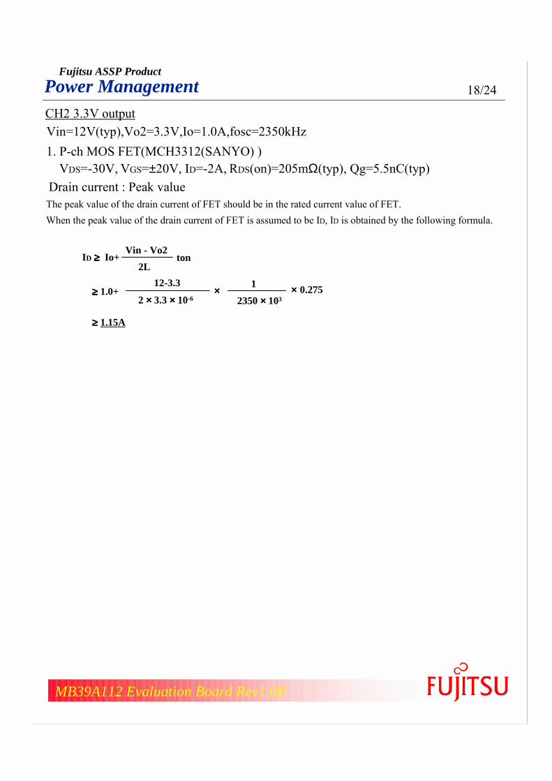
Vin=12V(typ),Vo2=3.3V,Io=1.0A,fosc=2350kHz1. P-ch MOS FET(MCH3312(SANYO) )
VDS=-30V, VGS=±20V, ID=-2A, RDS(on)=205mΩ(typ), Qg=5.5nC(typ)Drain current : Peak value
The peak value of the drain current of FET should be in the rated current value of FET.When the peak value of the drain current of FET is assumed to be ID, ID is obtained by the following formula.
Vin - Vo22L
ton
≥≥≥≥ 1.0+2 ×××× 3.3 ×××× 10-6
12-3.3××××
2350 ×××× 103
1 ×××× 0.275
ID ≥≥≥≥ Io+
≥≥≥≥ 1.15A
CH2 3.3V output

Fujitsu ASSP Product
19/24Power Management
MB39A112 Evaluation Board Rev1.0E
2. Inductor(A916CY-3R3M : TOKO) 3.3µH(tolerance : ±20%), rated current= 2.57A
L value in the full-load current condition:It is set that the peak to peak value of the ripple current becomes 1/2 or less of load currents.
Load current value which becomes continuous current condition.
Ripple current : peak value The peak value of the ripple current should be in the rated current value of the inductor. When the peak value of the ripple current is assumed to be IL, IL is obtained by the following formula.
Ripple current : peak to peak value When the peak to peak value of the ripple current is assumed to be ∆IL, ∆IL is obtained by the following formula.
L ≥≥≥≥2(Vin - Vo2)
Ioton
2 ××××(12-3.3)1.0
×××× 0.275××××2350 ×××× 103
1≥≥≥≥
≥≥≥≥ 2.04µµµµH
Io ≥≥≥≥2L
Vo2toff
2 ×××× 3.3 ×××× 10-6
3.3 ××××2350 ×××× 103
1××××(1-0.275)≥≥≥≥
≥≥≥≥ 0.15A
Vin - Vo22L
ton
≥≥≥≥ 1.0 +2 ×××× 3.3 ×××× 10-6
12-3.3××××
2350 ×××× 103
1×××× 0.275
IL ≥≥≥≥ Io+
≥≥≥≥ 1.15A
Vin - Vo2L
ton
=3.3 ×××× 10-6
12-3.3××××
2350 ×××× 103
1
∆∆∆∆IL =
≅≅≅≅ 0.309A
×××× 0.275

Fujitsu ASSP Product
20/24Power Management
MB39A112 Evaluation Board Rev1.0E
3. Flyback Diode (SBE001: SANYO) VR=30V, IO =2.0A, IFSM =20A, VF=0.55V, at IF=2.0A
IDi ≥≥≥≥ Io ×××× (1- ) = 1.0 ×××× (1 - 0.275 ) ≅≅≅≅ 0.725A
Vo22L
toff)(Io+IDip ≥≥≥≥ ≅≅≅≅ 1.15A
VinVo2
VR should be a value which satisfies the input voltage enough. →30VDiode average current IDi is obtained by the following formula.
Diode peak current IDip is obtained by the following formula.

Fujitsu ASSP Product
21/24Power Management
MB39A112 Evaluation Board Rev1.0E
Vin=12V(typ),Vo3=5V,Io=0.3A,fosc=2350kHz1. P-ch MOS FET(MCH3312(SANYO) )
VDS=-30V, VGS=±20V, ID=-1A, RDS(on)=720mΩ(typ), Qg=2.6nC(typ)Drain current : Peak value
The peak value of the drain current of FET should be in the rated current value of FET.When the peak value of the drain current of FET is assumed to be ID, ID is obtained by the following formula.
Vin - Vo32L
ton
≥≥≥≥ 0.3+2 ×××× 10 ×××× 10-6
12-5××××
2350 ×××× 103
1 ×××× 0.417
ID ≥≥≥≥ Io+
≥≥≥≥ 0.36A
CH3 5V output

Fujitsu ASSP Product
22/24Power Management
MB39A112 Evaluation Board Rev1.0E
2. Inductor(A916CY-100M : TOKO) 10µH(tolerance : ±20%), rated current= 1.49A
L value in the full-load current condition:It is set that the peak to peak value of the ripple current becomes 1/2 or less of load currents.
Load current value which becomes continuous current condition.
Ripple current : peak value The peak value of the ripple current should be in the rated current value of the inductor. When the peak value of the ripple current is assumed to be IL, IL is obtained by the following formula.
Ripple current : peak to peak value When the peak to peak value of the ripple current is assumed to be ∆IL, ∆IL is obtained by the following formula.
L ≥≥≥≥2(Vin - Vo3)
Ioton
2 ××××(12-5)0.3
×××× 0.417 ××××2350 ×××× 103
1≥≥≥≥
≥≥≥≥ 8.28µµµµH
Io ≥≥≥≥2L
Vo3toff
2 ×××× 10 ×××× 10-6
5 ××××2350 ×××× 103
1××××(1-0.417)≥≥≥≥
≥≥≥≥ 62.0mA
Vin - Vo32L
ton
≥≥≥≥ 0.3 +2 ×××× 10 ×××× 10-6
12-5××××
2350 ×××× 103
1 ×××× 0.417
IL ≥≥≥≥ Io+
≥≥≥≥ 0.36A
Vin - Vo3L
ton
=10 ×××× 10-6
12-5××××
2350 ×××× 103
1
∆∆∆∆IL =
≅≅≅≅ 0.124A
×××× 0.417

Fujitsu ASSP Product
23/24Power Management
MB39A112 Evaluation Board Rev1.0E
3. Flyback Diode (SBS005: SANYO) VR=30V, IO =1.0A, IFSM =10A, VF=0.35V, at IF=0.5A
IDi ≥≥≥≥ Io ×××× (1- ) = 0.3 ×××× (1 – 0.417 ) ≅≅≅≅ 0.175A
Vo12L
toff)(Io+IDip ≥≥≥≥ ≅≅≅≅ 0.36A
VinVo3
VR should be a value which satisfies the input voltage enough →30VDiode average current IDi is obtained by the following formula.
Diode peak current IDip is obtained by the following formula.
Fujitsu ASSP Product
24/24Power Management
MB39A112 Evaluation Board Rev1.0E
All Rights Reserved.The contents of this document are subject to change without notice. Customers are advised to consult with FUJITSU
sales representatives before ordering.The information and circuit diagrams in this document are presented as examples of semiconductor device
applications, and are not intended to be incorporated in devices for actual use.Also, FUJITSU is unable to assume responsibility for infringement of any patent rights or other rights of third parties arising from the use of this information or circuit diagrams.FUJITSU semiconductor devices are intended for use in standard applications (computers, office automation and
other office equipment, industrial, communications, and measurement equipment, personal or household devices, etc.).
CAUTION:Customers considering the use of our products in special applications where failure or abnormal operation may
directly affect human lives or cause physical injury or property damage, or where extremely high levels of reliability are demanded (such as aerospace systems, atomic energy controls, sea floor repeaters, vehicle operating controls, medical devices for life support, etc.) are requested to consult with FUJITSU sales representatives before such use. The company will not be responsible for damages arising from such use without prior approval.
Any semiconductor devices have an inherent chance of failure. You must protect against injury, damage or loss from such failures by incorporating safety design measures into your facility and equipment such as redundancy, fire protection, and prevention of over-current levels and other abnormal operating conditions.
If any products described in this document represent goods or technologies subject to certain restrictions on export under the Foreign Exchange and Foreign Trade Law of Japan, the prior authorization by Japanese government will be required for export of those products from Japan.
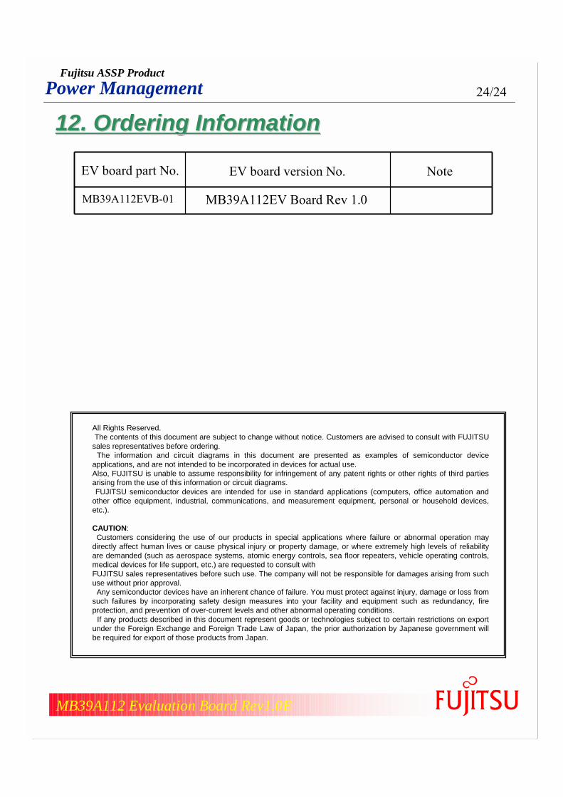
MB39A112EVB-01
EV board part No. EV board version No.
MB39A112EV Board Rev 1.0
Note
12. 12. Ordering InformationOrdering Information


![AK7734 Evaluation Board Rev - AKM Evaluation Board Rev.1 AKD7734-A [AKD7734-A] 2011/07 - 2 - Evaluation Board Diagram Board Diagram +12V-12V ...](https://static.fdocuments.net/doc/165x107/5c03e45309d3f203258d6861/ak7734-evaluation-board-rev-akm-evaluation-board-rev1-akd7734-a-akd7734-a-201107.jpg)