EVAL-1ED020I12F2-DB user guide
28
User Guide EVAL-1ED020I12F2-DB Please read the Important notice and the Safety precautions and the Warnings Revision 1.1 www.infineon.com page 1 of 28 2021-05-25 UG-2021-27 EVAL-1ED020I12F2-DB user guide Isolated driver daughter board to evaluate 1200 V CoolSiC™ MOSFET About this document Scope and purpose This user guide explains how to operate the evaluation board “EVAL-1ED020I12F2-DB” (daughterboard) together with the “Evaluation platform 1200V CoolSiC™ MOSFET in TO247 3pin / 4pin Rev. 2.” (motherboard) Intended audience This document is intended for owners and users of the evaluation board. Evaluation Board This board is to be used during design-in tasks, for evaluation and measurement of product characteristics, and proof of data sheet specifications. Note: PCB and auxiliary circuits are NOT optimized for final customer design.
Transcript of EVAL-1ED020I12F2-DB user guide

User Guide EVAL-1ED020I12F2-DB Please read the Important notice and the Safety precautions and the Warnings Revision 1.1
www.infineon.com page 1 of 28 2021-05-25
UG-2021-27
EVAL-1ED020I12F2-DB user guide
Isolated driver daughter board to evaluate 1200 V CoolSiC™ MOSFET
About this document
Scope and purpose
This user guide explains how to operate the evaluation board “EVAL-1ED020I12F2-DB” (daughterboard) together with the “Evaluation platform 1200V CoolSiC™ MOSFET in TO247 3pin / 4pin Rev. 2.” (motherboard)
Intended audience
This document is intended for owners and users of the evaluation board.
Evaluation Board
This board is to be used during design-in tasks, for evaluation and measurement of product characteristics, and
proof of data sheet specifications.
Note: PCB and auxiliary circuits are NOT optimized for final customer design.

User Guide EVAL-1ED020I12F2-DB 2 of 28 Revision 1.1
2021-05-25
EVAL-1ED020I12F2-DB user guide Isolated driver daughter board to evaluate 1200 V CoolSiC™ MOSFET
Important notice
Important notice
“Evaluation Boards and Reference Boards” shall mean products embedded on a printed circuit board
(PCB) for demonstration and/or evaluation purposes, which include, without limitation, demonstration, reference and evaluation boards, kits and design (collectively referred to as “Reference Board”).
Environmental conditions have been considered in the design of the Evaluation Boards and Reference Boards provided by Infineon Technologies. The design of the Evaluation Boards and Reference Boards has been tested by Infineon Technologies only as described in this document. The design is not qualified
in terms of safety requirements, manufacturing and operation over the entire operating temperature
range or lifetime. The Evaluation Boards and Reference Boards provided by Infineon Technologies are subject to functional
testing only under typical load conditions. Evaluation Boards and Reference Boards are not subject to the
same procedures as regular products regarding returned material analysis (RMA), process change notification (PCN) and product discontinuation (PD).
Evaluation Boards and Reference Boards are not commercialized products, and are solely intended for
evaluation and testing purposes. In particular, they shall not be used for reliability testing or production. The Evaluation Boards and Reference Boards may therefore not comply with CE or similar standards
(including but not limited to the EMC Directive 2004/EC/108 and the EMC Act) and may not fulfill other requirements of the country in which they are operated by the customer. The customer shall ensure that
all Evaluation Boards and Reference Boards will be handled in a way which is compliant with the relevant
requirements and standards of the country in which they are operated.
The Evaluation Boards and Reference Boards as well as the information provided in this document are
addressed only to qualified and skilled technical staff, for laboratory usage, and shall be used and
managed according to the terms and conditions set forth in this document and in other related
documentation supplied with the respective Evaluation Board or Reference Board. It is the responsibility of the customer’s technical departments to evaluate the suitability of the
Evaluation Boards and Reference Boards for the intended application, and to evaluate the completeness
and correctness of the information provided in this document with respect to such application.
The customer is obliged to ensure that the use of the Evaluation Boards and Reference Boards does not cause any harm to persons or third party property.
The Evaluation Boards and Reference Boards and any information in this document is provided "as is" and Infineon Technologies disclaims any warranties, express or implied, including but not limited to
warranties of non-infringement of third party rights and implied warranties of fitness for any purpose, or for merchantability.
Infineon Technologies shall not be responsible for any damages resulting from the use of the Evaluation Boards and Reference Boards and/or from any information provided in this document. The customer is
obliged to defend, indemnify and hold Infineon Technologies harmless from and against any claims or damages arising out of or resulting from any use thereof.
Infineon Technologies reserves the right to modify this document and/or any information provided herein at any time without further notice.

User Guide EVAL-1ED020I12F2-DB 3 of 28 Revision 1.1
2021-05-25
EVAL-1ED020I12F2-DB user guide Isolated driver daughter board to evaluate 1200 V CoolSiC™ MOSFET
Safety precautions
Safety precautions
Note: Please note the following warnings regarding the hazards associated with development systems.
Table 1 Safety precautions
Warning: The DC link potential of this board is up to 1200 VDC. When measuring voltage waveforms by oscilloscope, high voltage differential probes must be used. Failure to do
so may result in personal injury or death.
Warning: The evaluation or reference board contains DC bus capacitors which take time to discharge after removal of the main supply. Before working on the drive system, wait five minutes for capacitors to discharge to safe voltage levels. Failure to
do so may result in personal injury or death. Darkened display LEDs are not an
indication that capacitors have discharged to safe voltage levels.
Warning: The evaluation or reference board is connected to the grid input during testing. Hence, high voltage differential probes must be used when measuring voltage
waveforms by oscilloscope. Failure to do so may result in personal injury or death.
Darkened display LEDs are not an indication that capacitors have discharged to safe
voltage levels.
Warning: Remove or disconnect power from the drive before you disconnect or reconnect wires, or perform maintenance work. Wait five minutes after removing
power to discharge the bus capacitors. Do not attempt to service the drive until the bus capacitors have discharged to zero. Failure to do so may result in personal injury or
death.
Caution: The heat sink and device surfaces of the evaluation or reference board may
become hot during testing. Hence, necessary precautions are required while handling
the board. Failure to comply may cause injury.
Caution: Only personnel familiar with the drive, power electronics and associated machinery should plan, install, commission and subsequently service the system.
Failure to comply may result in personal injury and/or equipment damage.
Caution: The evaluation or reference board contains parts and assemblies sensitive to
electrostatic discharge (ESD). Electrostatic control precautions are required when
installing, testing, servicing or repairing the assembly. Component damage may result if ESD control procedures are not followed. If you are not familiar with electrostatic
control procedures, refer to the applicable ESD protection handbooks and guidelines.
Caution: A drive that is incorrectly applied or installed can lead to component damage
or reduction in product lifetime. Wiring or application errors such as undersizing the motor, supplying an incorrect or inadequate AC supply, or excessive ambient
temperatures may result in system malfunction.
Caution: The evaluation or reference board is shipped with packing materials that need to be removed prior to installation. Failure to remove all packing materials that are unnecessary for system installation may result in overheating or abnormal
operating conditions.

User Guide EVAL-1ED020I12F2-DB 4 of 28 Revision 1.1
2021-05-25
EVAL-1ED020I12F2-DB user guide Isolated driver daughter board to evaluate 1200 V CoolSiC™ MOSFET
Table of contents
Table of contents
About this document ....................................................................................................................... 1
Important notice ............................................................................................................................ 2
Safety precautions .......................................................................................................................... 3
Table of contents ............................................................................................................................ 4
1 The board at a glance .............................................................................................................. 5 1.1 Delivery content ...................................................................................................................................... 7
1.2 Block diagram .......................................................................................................................................... 7
1.3 Main features ........................................................................................................................................... 9 1.4 Board parameters and technical data .................................................................................................... 9
2 System and functional desription ........................................................................................... 10 2.1 Use of the daughterboard ..................................................................................................................... 10
2.1.1 Stand-alone board ........................................................................................................................... 10 2.1.2 Usage together with motherboard .................................................................................................. 10
2.2 Description of the functional blocks ..................................................................................................... 12
2.2.1 Basic operation ................................................................................................................................ 12 2.2.2 First steps for start up ...................................................................................................................... 14
3 System design....................................................................................................................... 15 3.1 Schematics ............................................................................................................................................ 15 3.2 Layout .................................................................................................................................................... 15
3.3 Bill of material ....................................................................................................................................... 18
3.4 Connector details .................................................................................................................................. 19
4 System performance ............................................................................................................. 21
4.1 Short circuit mesurements ................................................................................................................... 21 4.1.1 Example measurement 1: switching resistive load......................................................................... 22 4.1.2 Example measurement 2: short circuit at low-side ........................................................................ 23
4.1.3 Example measurement 3: short circuit at high-side ....................................................................... 24
5 References and appendices .................................................................................................... 26 5.1 Abbreviations and definitions ............................................................................................................... 26
5.2 References ............................................................................................................................................. 26
5.3 Additional information .......................................................................................................................... 26
Revision history ............................................................................................................................. 27

User Guide EVAL-1ED020I12F2-DB 5 of 28 Revision 1.1
2021-05-25
EVAL-1ED020I12F2-DB user guide Isolated driver daughter board to evaluate 1200 V CoolSiC™ MOSFET
The board at a glance
1 The board at a glance
The evaluation board “EVAL-1ED020I12F2-DB” is part of the CoolSiC™ evaluation platform second revision.
This platform was developed to show the optimal driving of the silicon carbide CoolSiC™ MOSFETs or other power switches in TO247 3-pin or 4-pin package. To achieve this target the design was split in two boards, one motherboard (evaluation platform) “EVAL-PS-DP-MAIN” and a flexible driver-card, e.g. (evaluation board “EVAL-1ED020I12F2-DB”). The modular approach enables future expansion of the platform with additional gate
driver cards. This means, the driver card is connected to the motherboard via connectors. In this way it is
possible to have different driver cards with of course different drivers which can work with one motherboard. The power switches can be connected via connectors as well.
The first driver card, based on the evaluation platform second revision, contains the EiceDRIVER™ IC 1ED020I12-F2 with an integrated active Miller clamp preventing unintended turn-on and a DESAT pin to protect the
application against damage through short circuit.
Figure 1 and Figure 2 shows the daughterboard EVAL-1ED020I12F2-DB, Figure 3 shows the CoolSiC™ evaluation platform.
Figure 1 Top view of evaluation daughterboard EVAL-1ED020I12F2-DB

User Guide EVAL-1ED020I12F2-DB 6 of 28 Revision 1.1
2021-05-25
EVAL-1ED020I12F2-DB user guide Isolated driver daughter board to evaluate 1200 V CoolSiC™ MOSFET
The board at a glance
Figure 2 Bottom view of evaluation daughterboard EVAL-1ED020I12F2-DB
A more detailed description please see in Chapter 1.2.
Figure 3 Top view complete solution (motherboard + daughterboard)

User Guide EVAL-1ED020I12F2-DB 7 of 28 Revision 1.1
2021-05-25
EVAL-1ED020I12F2-DB user guide Isolated driver daughter board to evaluate 1200 V CoolSiC™ MOSFET
The board at a glance
Figure 4 Bottom view motherboard
1.1 Delivery content
Content of delivery is the EVAL-1ED020I12F2-DB board packed in a box. The evaluation platform EVAL-PS-DP-MAIN can be ordered seperatly. Since different daughterboards, such as EVAL-1ED020I12F2-DB, can be driven
with one evaluation platform (motherboard), this arrangement allows a flexible choice of daughterboards with the motherboard.
1.2 Block diagram
The block diagram of the EVAL-1ED020I12F2-DB board is depicted in Figure 5.

User Guide EVAL-1ED020I12F2-DB 8 of 28 Revision 1.1
2021-05-25
EVAL-1ED020I12F2-DB user guide Isolated driver daughter board to evaluate 1200 V CoolSiC™ MOSFET
The board at a glance
Figure 5 Blockdiagramm of EVAL-1ED020I12F2-DB
The connector X202 (see Figure 5) connects the daughter board with all signals from the primary side (low-
voltage side) of the gate driver, like IN+, IN-, /Fault, /RDY, VCC1 and GND1 of both drivers to the evaluation
platform and the corresponding connector X100 on this platform
As interface to the power switches acting the connectors X200 and X201 (see Figure 5) with the gate signal, the
source connection and the drain connection for the DESAT function. Connector X200 serves the high-side
switch, X201 the low-side switch. At the same time, the respective supply voltages for the drivers ( VCC2, VEE2 and GND2) are connected.
GND2_LS
GND2_HS
X202
X201
VCC2_LS
VEE2_LS
Gate_LS
X200
VCC2_HS
VEE2_HS
Gate_HS
1E
D0
20I1
2-F
2
DESAT
OUT
CLAMP
EVAL-1ED020I12F2-DB
High-side
Low-side
Primary-side Secondary-sideIsolation barrier
1E
D0
20I1
2-F
2
DESAT
OUT
CLAMP
RGate
RDESAT
0
CDESAT
RGate
RDESAT
0
CDESAT
DDESAT
DDESAT

User Guide EVAL-1ED020I12F2-DB 9 of 28 Revision 1.1
2021-05-25
EVAL-1ED020I12F2-DB user guide Isolated driver daughter board to evaluate 1200 V CoolSiC™ MOSFET
The board at a glance
1.3 Main features
• Two seperate single-channel isolated gate driver
• Each driver has 2.4 A rail-to-rail outputs
• For 600 V / 1200 V power switches, like MOSFETs, IGBTs or SiC MOSFETs
• DESAT-detection for overcurrent / short-circuit protection
• Active Miller clamp
1.4 Board parameters and technical data
The key specifications of this board are displayed in Table 2.
Table 2 Parameter
Parameter Symbol Value
(max)
Unit Test condition
Positive power supply output side VCC2 20 V 1)
Negative power supply output side VEE2 -12 V 1)
Maximum power supply voltage output side
(VCC2 – VEE2)
Vmax2 28 V
Positive power supply input side VCC1 6.5 V
Input-to-output isolation voltage VISO 1200 V
Gate driver high output maximum current
(per channel)
IOUT 2.4 A t = 2 µs
Gate & clamp driver low output maximum current (per
channel)
IOUT 2.4 A t = 2 µs
Mechanical dimensions length 54 mm
width 29 mm
hight 19 mm With connectors
1) With respect to GND2
All this technical elctrical parameter shown in Table 2 are related to the Infineon gate driver IC 1ED020I12-F2.

User Guide EVAL-1ED020I12F2-DB 10 of 28 Revision 1.1
2021-05-25
EVAL-1ED020I12F2-DB user guide Isolated driver daughter board to evaluate 1200 V CoolSiC™ MOSFET
System and functional desription
2 System and functional desription
2.1 Use of the daughterboard
The daughter board can be used in two different ways.
1.) Stand-alone board
2.) Usage together with motherboard
2.1.1 Stand-alone board
In the case of stand-alone usage, the application is structured in such a way that the following must be developed: circuit board with corresponding plug connectors, galvanically isolated power supplies,
connections for the high-voltage power switches, and the connections for the low voltage side. The technical
parameters in Table 2 have to be considered. Please also note that there is an insulation gap between the low voltage and the high voltage side, as shown in Figure 5.
2.1.2 Usage together with motherboard
If the motherboard, EVAL-PS-DP-MAIN, is used, commissioning is simple, as the daughterboard was specifically designed to be used together with it. Figure 3 shows the top view of this motherboard.
Please read the data sheet for the motherboard before starting up.
The motherboard is divided into two sections: the primary supply side on the left and the power (high-voltage)
circuit indicated as secondary side on the right. They are separated by the white marker line. On the primary
side, four connectors are visible: X105, X102, X101 and X100. The 12 V supply voltage on the low-voltage side is connected (red-colored, positive pole) to X102 and X105. Three other voltages for the two drivers are generated from this 12 V power supply: VCC1, VCC2 and VEE2.
VCC2 and VEE2 are galvanically separated from each other and also from the other voltages.
The connector X100 connect the primary side of the mainboard and the primary side of the EVAL-1ED020I12F2-
DB which each other. All importand signals from EVAL-1ED020I12F2-DB like IN+, IN-, /Fault and /RDY of both drivers will be provided via X100 from the motherboard to the EVAL-1ED020I12F2-DB. At the motherboard side
this signals are delivered from connector X101, which is the interface to the outside world, for example a µController.
The EVAL-1ED020I12F2-DB is supplied with supply voltages VCC1, VCC2 and VEE2 via DC/DC converters. These
connectors are mounted on the motherboard and enable a flexible supply. The decision about which driving
voltages (VCC2 and VEE2) are to be connected to the EVAL-1ED020I12F2-DB via connectors X107 and X110 is made via jumpers on the pin headers X108 (low-side) and X106 (high-side). VCC1 is provided via connector
X100.
The power supply can be configured with two jumpers on the high-side and two jumpers on the low-side according to the requirements of the drivers at the EVAL-1ED020I12F2-DB or other daughterboards and the downstream power switches.
The possible configurations for setting the driving voltages (VCC2 and VEE2) via two jumpers are visualized in Table 3 and Figure 6.

User Guide EVAL-1ED020I12F2-DB 11 of 28 Revision 1.1
2021-05-25
EVAL-1ED020I12F2-DB user guide Isolated driver daughter board to evaluate 1200 V CoolSiC™ MOSFET
System and functional desription
Table 3 Jumper configurations for powersupply of EVAL-1ED020I12F2-DB
+ADJ +20V 0V -5V -ADJ
X X
X X
X X
X X
X X
X X
The settings for the adjustable driver voltages are made using the potentiometer R105 and R102 for the high-side driver and with potentiometer R108 and R107 for the low-side driver of the EVAL-
1ED020I12F2-DB. R102 and R106 adjust the positive voltage (VCC2) of the drivers in the range between 7.5 V and +20V, R105 and R107 adjast the negative voltage (VEE2) in the range between -1 V and -4.5 V.
Figure 6 Jumper and potentiometer for voltage settings VCC2 and VEE2

User Guide EVAL-1ED020I12F2-DB 12 of 28 Revision 1.1
2021-05-25
EVAL-1ED020I12F2-DB user guide Isolated driver daughter board to evaluate 1200 V CoolSiC™ MOSFET
System and functional desription
2.2 Description of the functional blocks
The description of the functional blocks of the daughterboard EVAL-1ED020I12F2-DB refer to Figure 5. All connections are shown only roughly, the detailed circuit is shown in Figure 8.
In principle, the board can be separated into two parts, the primary and the secondary side. The primary side describes the low voltage area, the secondary the high-voltage area, which directly controls the power switch.
No components or electrical lines should be placed in the isolation barrier, as otherwise the insulation between input and output (primary and secondary side) cannot be guaranteed.
Furthermore, two gate driver ICs, 1ED020I12-F2, which can generally be operated separately, are positioned on the board. In connection with the motherboard, this two drivers working in a half-bridge configuration, so that
one IC works as the high-side driver and the other IC as the low-side driver.
The primary side comprises the connector X202 as well as all necessary lines and passive components which are necessary for the safe operation of the gate drivers. Connector X202 delivers all the necessary control
signals (IN+, IN-, /FLT, RDY and /RST) as well as the electrical power (VCC1 and GND1) to the primary side of both gate driver ICs. More detailed information can be found in Chapter 4.4, Table 5.
The connectors X200 and X201 on the secondary side are used to supply the two drivers with the secondary power supply which is required for the gate voltages and are the connection to the power switches. Each gate
driver has its own power supply, they are galvanically isolated to each other. More detailed information about the connectors X200 and X201 can be found in Chapter 4.4, Table 6 and Table 7.
Via RDESAT; DDSAT and X200-10/X201-10, the DESAT inputs of the gate drivers are connected to the drain when used
with of SiC MOSFET or MOSFET, or to the Collector when used with IGBT. This DESAT function protects the
power switches against over current situations.
The outputs “OUT” of the gate drivers are connected via RGate and X200-1,2/X201-1,2 to the gate of the corresponding power switch and delivers the gate voltage to drive the power switches.
Outputs “CLAMP” are connected via zero ohm resistors (0 Ω) to the gate resistors. The reason is, if clamp
function is not required, resistors just can be removed.
2.2.1 Basic operation
Please note that the entire evaluation platform was designed for double-pulse tests and short-circuit tests only. The evaluation platform is unsuitable for long-term tests, as the power switches are not soldered. Figure 7 presents a possible configuration of this combination of mother- and daughterboard.

User Guide EVAL-1ED020I12F2-DB 13 of 28 Revision 1.1
2021-05-25
EVAL-1ED020I12F2-DB user guide Isolated driver daughter board to evaluate 1200 V CoolSiC™ MOSFET
System and functional desription
Figure 7 Motherboard equipped wit daughterboard and SiC MOSFET´s for low-side measurements
Especially in this configuration (wiring of the load) the arrangement can be used for low-side measurements. Power switch Q2 is now the DUT (device under test).
A configuration for high-side measurements is shown in Chapter 4.1.3.
X202
Gate_LS
Gate_HS
1E
D0
20I1
2-F
2DESAT
OUT
CLAMP
EVAL-1ED020I12F2-DB
(daughter board)
High-side
Low-side
RGate
RDESAT
0
CDESAT
RGate
RDESAT
0
CDESAT
DDESAT
DDESAT
1E
D0
20I1
2-F
2
DESAT
OUT
CLAMP
D
G
S
D
G
S
VDC
X200
X201
X101
+ -
LoadX150 X151 X152
RShunt
X105
X102
800 V
+
-
12 V
+ 12V
+ V
DC
GND1
Mid
po
int
(ph
as
e)
GN
D-S
ec
µController
Evaluation platform
(mother board)
Q1
Q2
phase

User Guide EVAL-1ED020I12F2-DB 14 of 28 Revision 1.1
2021-05-25
EVAL-1ED020I12F2-DB user guide Isolated driver daughter board to evaluate 1200 V CoolSiC™ MOSFET
System and functional desription
2.2.2 First steps for start up
Before the whole application can be put into operation, the following commissioning steps should be observed:
1.) Take empty motherboard out of the box
2.) Connect 12 V corresponding to Figure 7
3.) Set the jumpers for driver voltages as described in Chapter 2.1.2, Table 3 and Figure 6, according to the needs of the corresponding drivers at the daughterboard
4.) If an adjustable powersupply has been selected, VCC2 and VEE2 has to be set by the potentiometer according to details described in Chapter 2.1.2, Table 3 and Figure 6
5.) Disconnect 12 V (to make all changes without power supply)
6.) Plugging in the daughterboard and the power switches
7.) Connect 12 V and µController interface (or other 5 V-compatible digital switching signals) to connector X101 (see Figure 7)
8.) Connect the high-voltage power supply (ensure that it is switched off !!) and load according to the requirements
Now the complete setup (motherboard + daughterboard) is ready for testing. If all safety conditions applicable
to the respective laboratory are complied with, the high voltage can be switched on and measurements can be started.

User Guide EVAL-1ED020I12F2-DB 15 of 28 Revision 1.1
2021-05-25
EVAL-1ED020I12F2-DB user guide Isolated driver daughter board to evaluate 1200 V CoolSiC™ MOSFET
System design
3 System design
3.1 Schematics
Figure 8 shows the drawing of the daughterboard 1ED020I12F2-DB.
Figure 8 Drawing of EVAL-1ED020I12F2-DB
3.2 Layout
The following figures present the different layers of the layout from the daughterboard EVAL-1ED020I12F2-DB. Due to the small dimensions of the design, a 4-layer layout was provided. The order from the top view: Top
layer, Layer 1, Layer 2, Bottom layer

User Guide EVAL-1ED020I12F2-DB 16 of 28 Revision 1.1
2021-05-25
EVAL-1ED020I12F2-DB user guide Isolated driver daughter board to evaluate 1200 V CoolSiC™ MOSFET
System design
Figure 9 Top layer of EVAL-1ED020I12F2-DB
Figure 10 Layer 1 of EVAL-1ED020I12F2-DB

User Guide EVAL-1ED020I12F2-DB 17 of 28 Revision 1.1
2021-05-25
EVAL-1ED020I12F2-DB user guide Isolated driver daughter board to evaluate 1200 V CoolSiC™ MOSFET
System design
Figure 11 Layer 2 of EVAL-1ED020I12F2-DB
Figure 12 Bottom layer of EVAL-1ED020I12F2-DB

User Guide EVAL-1ED020I12F2-DB 18 of 28 Revision 1.1
2021-05-25
EVAL-1ED020I12F2-DB user guide Isolated driver daughter board to evaluate 1200 V CoolSiC™ MOSFET
System design
3.3 Bill of material
The complete bill of material is available on the download section of the Infineon homepage. A log-in
is required to download this material.
Table 4 BOM of the evaluation board EVAL-1ED020I12F2-DB
comment Ref Designator Description Manufacturer Manufacturer P/N
1 uF C1, C7 Surface Mount Ceramic Capacitor Automotive
Grade
AVX 478-6357-2-ND
4.7 uF C2, C6, C8, C12,
C13, C14
TDK multilayer ceramic chip capacitor_Soft
termiantion_Automotive
grade_CGA serie
TDK Corporation 445-181410-1-ND
33 pF C3, C9 High temperature
application CGA series
TDK Corporation 445-12409-1-ND
100 pF C4, C5, C10, C11 Surface Mount Multilayer Ceramic Chip
Capacitor
Kemet
BAT165 D1, D2, D4, D5, D6, D7, D8, D10,
D11, D12
Medium Power AF
Schottky Diode
Infineon
Technologies
BAT165E6327HTSA1TR-
ND
S3N D3, D9 General-Purpose
Rectifier, VRRM 1200V
ON
Semiconductor
S3NCT-ND
4.7 k R1, R7, R9, R15 Standard Thick Film
Chip Resistor
Vishay
9.1 k R2, R10 Standard Thick Film
Chip Resistor
Vishay
0 R R3, R6, R11, R14 General Purpose Chip
Resistor
Yageo 311-0.0GRTR-ND
0 R R4, R12 Solder Stability Chip
Resistor
Bourns CR0603-J/-000ELFTR-
ND
10 R R5, R8, R13, R16 General Purpose Chip
Resistor Yageo
1ED020I12-F2 U1, U2 Galvanically isolated
single-channel IGBT driver provides
protection features like
desaturation protection, active Miller clamping
and active shut down
Infineon
Technologies
1ED020I12F2XUMA1CT-
ND
TSW-105-07-L-D X200, X201 Through hole .025'' SQ Post Header, 2.54mm pitch, 10 pin, vertical,
double row
Samtec SAM1030-05-ND
HTSW-110-07-L-
D
X202 Hi -Temp Strip,Through hole .025'' SQ Post
Samtec SAM12659-ND

User Guide EVAL-1ED020I12F2-DB 19 of 28 Revision 1.1
2021-05-25
EVAL-1ED020I12F2-DB user guide Isolated driver daughter board to evaluate 1200 V CoolSiC™ MOSFET
System design
comment Ref Designator Description Manufacturer Manufacturer P/N
Header, 2.54mm pitch,
20 pin, vertical, double
row
TLW-102-05-G-S X203, X204 Through hole .025'' SQ Post Header, 2.54mm
pitch, 2 pin, vertical,
single row
Samtec SAM8736-ND
3.4 Connector details
The following Tables 5, 6 and 7 list the respective signal assignments corresponding to the plug connections.
Table 5 Connector X202 (Primary side)
PIN Label Function
1 VCC1 Power supply primary side
2 VCC1 Power supply primary side
3 nc
4 nc
5 GND_P Ground primary side
6 GND_P Ground primary side
7 IN+ T Positive driver input IN+ high-side
8 IN- T Negative driver input IN- high-side
9 /RST_T Reset input high-side, low active
10 /FLT_T Fault output high-side, low active
11 nc
12 RDY_T RDY output high-side
13 RDY_B RDY output low-side
14 /FLT_B Fault output low-side, low active
15 VCC1 Power supply primary side
16 /RST_B Reset input low side, low active
17 IN- B Negative driver input IN- low-side
18 IN+ B Positive driver input IN+ low-side
19 nc
20 nc

User Guide EVAL-1ED020I12F2-DB 20 of 28 Revision 1.1
2021-05-25
EVAL-1ED020I12F2-DB user guide Isolated driver daughter board to evaluate 1200 V CoolSiC™ MOSFET
System design
Table 6 Connector X200 (High-side power switch – secondary side)
PIN Label Function
1 HS_Gate Gate voltage high-side
!! HIGH VOLTAGE!!
2 HS_Gate Gate voltage high-side
!! HIGH VOLTAGE!!
3 HS_VON (0..+20 V) Positive power supply (VCC2) high-side
!! HIGH VOLTAGE!!
4 HS_GND_SEC Ground high-side secondary side
!! HIGH VOLTAGE!!
5 HS_VOFF (0..-5 V) Negative power supply (VEE2) high-side
6 HS_GND_SEC Ground high-side secondary side
!! HIGH VOLTAGE!!
7
8
9
10 HS_HV_VDC Drain (collector) interface for DESAT high-
side !! HIGH VOLTAGE!!
Table 7 Connector X201 (Low-side power switch – secondary side)
PIN Label Function
1 LS_Gate Gate voltage low-side
2 LS_Gate Gate voltage low-side
3 LS_VON (0..+20 V) Positive power supply (VCC2) low-side
4 LS_GND_SEC Ground low-side secondary side
5 LS_VOFF (0..-5 V) Negative power supply (VEE2) high-side
6 LS_GND_SEC Ground high-side secondary side
7
8
9
10 HV_Midpoint (phase) Drain (collector) interface for DESAT low- side
!! HIGH VOLTAGE!!

User Guide EVAL-1ED020I12F2-DB 21 of 28 Revision 1.1
2021-05-25
EVAL-1ED020I12F2-DB user guide Isolated driver daughter board to evaluate 1200 V CoolSiC™ MOSFET
System performance
4 System performance
In Chapter 4 some measurement results are introduced. These measurements are intended to demonstrate that the the system is fully operationa,l and that clear measurement data can be derived.
4.1 Short circuit mesurements
Since the overcurrent or short-circuit protection is an important function of the gate driver IC 1ED020I12-F2, some measurements are presented here. Figure 13 illustrades the main functionality of the overcurrent
shutdown using DESAT functionality.
Figure 13 Circriuty for DESAT functionality
On the left-hand side of Figure 13, a section of the internal circuitry of the gate driver is shown schematically.
The internal power source delivers a constant current of around 500 µA and is connected to the internal comparator and the DESAT pin. A charging capacitor CDESAT, a resistor RDESAT and a fast high voltage diode VF with the smallest possible capacitance are connected to the external DESAT -sense pin as shown in Figure 13. The
cathode of the high voltage diode is connected directly to the drain of the SiC MOSFET. This diode prevents the high voltage from reaching the gate driver.
The DESAT module only works when the driver is switched on, i.e. when the gate driver switches on the power
switch via input “IN”. In this case, a so-called leading-edge blanking time (tDESATleb) is expected, during which no action is taken. This represents a delay time, which ignores certain disturbances or oscillations caused by the switch-on process. Of course, no short circuit should be displayed here.
After that time, the capacitor is released and a part of the current from the internal current source charges the capacitor. Another part of the current flows through the resistor and the diode through the drain. In normal
operation (no error case) an equilibrium is established. The voltage VC_DESAT can be calculated using Equation 2
from Figure 14, and should be significantly lower than 9 V.
If an error occurs, e.g. an excessively high current due to a short circuit, the voltage VDS (from SiC MOSFET in
this case) will increase. If the voltage at the drain is too high, the diode VF closes and the internal current source will charge the capacitor CDESAT only. If the voltage on the capacitor exceeds 9 V, the internal comparator will
D
G
S
RDESAT
IDESAT 500µA
9 VVREF
xComparator
VDS
VFVR_DESAT
CD
ES
AT
VC_DESAT
DESAT
sense pin
DESAT
control
1EDI020I12-F2
IN
User Guide EVAL-1ED020I12F2-DB 22 of 28 Revision 1.1
2021-05-25
EVAL-1ED020I12F2-DB user guide Isolated driver daughter board to evaluate 1200 V CoolSiC™ MOSFET
System performance
switch off the output of the driver latching. This means the switch stays off, no matter what happens at the “IN” input. The driver must be released again by RESET.
Due to the constant current of the internal current source, the charging time of the capacitor can be calculated using Equation 1 from Figure 14. It should be noted that any capacitance which is in some
way connected to the DESAT pin (protection diodes, capacitances via layout, capacitance of high
voltage diode VF) must also be considered. For example, charges from the drain can also reach the capacitor VC_DESAT through the capacitance of the diode VF, and thus shorten the charging time.
Figure 14 Equations to describe DESAT behavior
4.1.1 Example measurement 1: switching resistive load
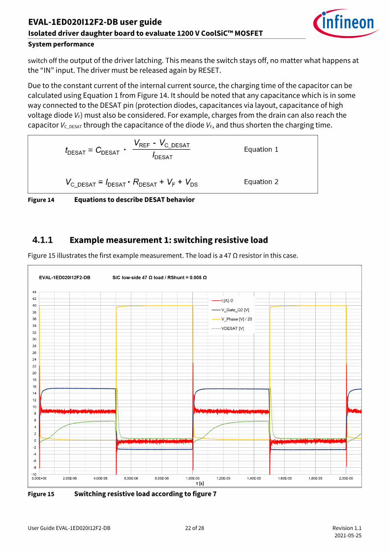
Figure 15 illustrates the first example measurement. The load is a 47 Ω resistor in this case.
Figure 15 Switching resistive load according to figure 7

User Guide EVAL-1ED020I12F2-DB 23 of 28 Revision 1.1
2021-05-25
EVAL-1ED020I12F2-DB user guide Isolated driver daughter board to evaluate 1200 V CoolSiC™ MOSFET
System performance
Figure 15 shows how the measurement works with an ohmic load resistor in a low-side configuration. As soon as the gate voltage rises (blue line) to 15 V (switch-on process), the phase voltage (yellow line) falls to below
1 V, and the drain current (red line) of Q2 (or load current) increases to approximately 17 A. The DESAT voltage ( green dashed line ) rises to almost 6 V after the leading-edge blanking time.
The switch-off process begins with the falling edge of the gate voltage. The phase voltage increases to
approximate 800 V, and the load current drops down to 0 A. The DESAT output switches off and discharges the DESAT capacitor. The short intermediate peak looks like a capacitive behavior of the diode VF and the very high du/dt (drain voltage) of approximately 23.400 V/µs.
4.1.2 Example measurement 2: short circuit at low-side
The second measurement example is shown in Figure 16 to and demonstrates a short-circuit measurement in
low-side configuration. In this case, the load as shown in Figure 7 is replaced by a short cable.
Figure 16 Short ciruit measurement at low-side configuration
The switch-on process is the same as in the previous measurement. The only difference is that no resistor is connected in between. The pulse length at the input of the driver is the same at 5 µs. As soon as the gate
voltage increases, the load current increases rapidly up to approxivmately 330 A. Due to the very high current, the phase voltage briefly drops from arround 800 V to 280 V, but recovers after several hundrets nanoseonds. It
can be observed clearly that the current strength decreases slightly. This is related to the fact that the MOSFET heats up, and thus the internal resistance increases.
The voltage on the DESAT pin behaves as described in Chapter 4.1. After the leading-edge blanking time
(tDESATleb), the DESAT capacitor (CDESAT) charges in time tDESAT. From a DESAT voltage of 9 V, the driver is switched is off internally. After another internal time delay (tDESATOUT), the output switches off and the current begins to decrease. In this setup, the entire process takes about 780 ns.

User Guide EVAL-1ED020I12F2-DB 24 of 28 Revision 1.1
2021-05-25
EVAL-1ED020I12F2-DB user guide Isolated driver daughter board to evaluate 1200 V CoolSiC™ MOSFET
System performance
4.1.3 Example measurement 3: short circuit at high-side
For a short-circuit measurement in the high-side configuration, the external circuitry of the system must be changed slightly, see Figure 17.
Figure 17 External circuit for high-side measurements
The first difference between the arrangements in Figure 7 and Figure 17 is that the switch Q1 is now the DUT. A
short cable is connected accordingly between X151 and RShunt. The digital signals from the µController should be connected in accordance with Table 5, so that the high-side driver is addressed. If everything is connected
correctly, a diagram similar as in Figure 18 should be derived.
X202
Gate_LS
Gate_HS
1E
D0
20I1
2-F
2
DESAT
OUT
CLAMP
EVAL-1ED020I12F2-DB
(daughter board)
High-side
Low-side
RGate
RDESAT
0
CDESAT
RGate
RDESAT
0
CDESAT
DDESAT
DDESAT
1E
D0
20I1
2-F
2
DESAT
OUT
CLAMP
D
G
S
D
G
S
VDC
X200
X201
X101
+ -
X150 X151 X152
RShunt
X105
X102
800 V
+
-
12 V
+ 12V
+ V
DC
GND1
Mid
po
int
(ph
as
e)
GN
D-S
ec
µController
Evaluation platform
(mother board)
Q1
Q2
phase

User Guide EVAL-1ED020I12F2-DB 25 of 28 Revision 1.1
2021-05-25
EVAL-1ED020I12F2-DB user guide Isolated driver daughter board to evaluate 1200 V CoolSiC™ MOSFET
System performance
Figure 18 Short ciruit measurement at high-side configuration
The measurement results shown in Figure 18 are similar to result in Chapter 4.1.2, Figure 16. The difference is that the phase voltage V_Phase increases from zero up to approximat 620 V when Q1 is switched on. Due to the
steep rise and the high value of the current, the full DC voltage of 800 V is not reached. Shortly after the increase, the phase voltage drops down again due to the very high current value. Similar to the low-side
measurement, the value of the current drops slightly due to the heating of the power switch, in this configuration SiC MOSFET Q1.
After approximately 760 ns, the output of the driver switches off.

User Guide EVAL-1ED020I12F2-DB 26 of 28 Revision 1.1
2021-05-25
EVAL-1ED020I12F2-DB user guide Isolated driver daughter board to evaluate 1200 V CoolSiC™ MOSFET
References and appendices
5 References and appendices
5.1 Abbreviations and definitions
Table 8 Abbreviations
Abbreviation Meaning
CE Conformité Européenne
EMI Electromagnetic interference
UL Underwriters Laboratories
DUT Device under test
5.2 References
5.3 Additional information
Body text.

User Guide EVAL-1ED020I12F2-DB 27 of 28 Revision 1.1
2021-05-25
EVAL-1ED020I12F2-DB user guide Isolated driver daughter board to evaluate 1200 V CoolSiC™ MOSFET
Revision history
Revision history
Document
version Date of release Description of changes
Revision 1.0 2021-05-20 Initial release
Revision 1.1 2021-05-25 Change footnote (Revision 1.x instead of v 1.x), add revision history

Trademarks All referenced product or service names and trademarks are the property of their respective owners.
Edition 2020-10-22
UG-2021-27
Published by
Infineon Technologies AG
81726 Munich, Germany
© 2021 Infineon Technologies AG.
All Rights Reserved.
Do you have a question about this
document?
Email: [email protected]
Document reference
For further information on the product, technology, delivery terms and conditions and prices please contact your nearest Infineon Technologies office (www.infineon.com). WARNINGS Due to technical requirements products may contain dangerous substances. For information on the types in question please contact your nearest Infineon Technologies office. Except as otherwise explicitly approved by Infineon Technologies in a written document signed by authorized representatives of Infineon Technologies, Infineon Technologies’ products may not be used in any applications where a failure of the product or any consequences of the use thereof can reasonably be expected to result in personal injury.