ESODAC Study for a new ESO Detector Array Controller.
13
ESODAC ESODAC Study for a new Study for a new ESO ESO D D etector etector A A rray rray C C ontroller ontroller
-
Upload
gwendolyn-dalton -
Category
Documents
-
view
222 -
download
1
Transcript of ESODAC Study for a new ESO Detector Array Controller.

ESODACESODAC
Study for a new Study for a new ESOESO DDetector etector AArray rray CControllerontroller

IntroductionIntroductionand Key Pointsand Key Points
Idea is to realize a modular system with a basic Front-end unit for a four channel system on Idea is to realize a modular system with a basic Front-end unit for a four channel system on one card of standard VME 6U size.one card of standard VME 6U size.
Power Consumption on Front-end less than 10 Watts.Power Consumption on Front-end less than 10 Watts.
Very low noise design anticipated.Very low noise design anticipated. Add on cards are 32 channels on a board of the same size and additional ~10 Watts of power Add on cards are 32 channels on a board of the same size and additional ~10 Watts of power
consumption.consumption.( Number of channels can be remotely set ).( Number of channels can be remotely set ).
There will be no processor on the front-end side.There will be no processor on the front-end side.
Data distribution on backend side possible – free topology .Data distribution on backend side possible – free topology .
Connection between Back and Front-end only by fibers.Connection between Back and Front-end only by fibers.
Weight below 1 Kg.Weight below 1 Kg.
This system should not require active cooling.This system should not require active cooling.

System DesignSystem Design

System BlockSystem Block
RxTx
RxTx
RxTx
RxTx
RxTx
RxTx
RxTx
RxTx
Back-End
Back-End PCI PCI
Front-End
Back-End PCI
Back-End VME
FPGA
FPGA
FPGA
FPGA
Front-End Basic Module
Front-End AQ Module
Front-End AQ Module
Fiber Duplex
Connection
?
Signal
Signal Clock Bias
Signal
Serial Links or Backplane Bus
FPGA
FPGA

Back-endBack-end
Function is based on the XILINX Virtex Pro FPGA XC2VP7 FF 672 .Function is based on the XILINX Virtex Pro FPGA XC2VP7 FF 672 .
Back-End PCI is a 64 Bit PCI board downscale to 32 Bit PCI possible.Back-End PCI is a 64 Bit PCI board downscale to 32 Bit PCI possible. FPGA contains PCI interface, protocol engine PCI to transceiversFPGA contains PCI interface, protocol engine PCI to transceivers
for communication and data reception and RocketIO transceivers.for communication and data reception and RocketIO transceivers. Direct interface from FPGA to PCI without glue logic.Direct interface from FPGA to PCI without glue logic.
Independent PCI master and PCI slave. Independent PCI master and PCI slave.
Communication and data transfers all on serial link.Communication and data transfers all on serial link.
Data rate on one channel between front and back-end ~ 200MByteData rate on one channel between front and back-end ~ 200MByteMore bandwith possible ( one FPGA contains 8 transceivers – space limit for PCI card size More bandwith possible ( one FPGA contains 8 transceivers – space limit for PCI card size might be four ).might be four ).
Routing capability by high speed fibers e.g. to VME or other systems.Routing capability by high speed fibers e.g. to VME or other systems.
Selective data reception and routing possible ( like in old times shift and add with IRACE ). Selective data reception and routing possible ( like in old times shift and add with IRACE ).

Front-End Front-End Basic Module Basic Module
The front-end Basic Module is based on the XILINX Virtex Pro FPGA XC2VP7 FF 672.The front-end Basic Module is based on the XILINX Virtex Pro FPGA XC2VP7 FF 672.
Main functions of this module are :Main functions of this module are : Communication Communication
Data transferData transfer
SequencerSequencer
Clock driver, biases and associated DAC’sClock driver, biases and associated DAC’s
Four data acquisition channels ( each either 16 or 18 Bit ADC’s ) and preampsFour data acquisition channels ( each either 16 or 18 Bit ADC’s ) and preamps
Utilities ( Markers, Synchronization …)Utilities ( Markers, Synchronization …)
TelemetryTelemetry

Front-End Front-End Basic Module Basic Module
Design ideas are :Design ideas are :
Communication and data transfer to the back-end is handled with the FPGA’s Gigabit Communication and data transfer to the back-end is handled with the FPGA’s Gigabit transceivers.transceivers.
Protocol engine to serial link contained within the FPGA.Protocol engine to serial link contained within the FPGA.
Sequencer is completely contained within the FPGA.Sequencer is completely contained within the FPGA. The digital clock driver lines of the sequencer connect out of the FPGA without glue logic to The digital clock driver lines of the sequencer connect out of the FPGA without glue logic to
the clock driver switches. Clock driver alternatives have to be evaluated, one possibility is the clock driver switches. Clock driver alternatives have to be evaluated, one possibility is type used in IRACE.type used in IRACE.
Sequencer will contain provisions for high speed external trigger inputs and status outputs.Sequencer will contain provisions for high speed external trigger inputs and status outputs.
The ADC outputs of the four acquisition channels connect without glue logic to the FPGA due The ADC outputs of the four acquisition channels connect without glue logic to the FPGA due to the high pin count available there. Favorable ADC’s are the AD76xx types from Analog to the high pin count available there. Favorable ADC’s are the AD76xx types from Analog Devices. The preamplifier is fully differential, input range will be +/- 2.5V. There will be no Devices. The preamplifier is fully differential, input range will be +/- 2.5V. There will be no clamp/sample implemented in the analog chain.clamp/sample implemented in the analog chain.
Provisions will be taken to incorporate different ADC types ( e.g. high speed lower resolution Provisions will be taken to incorporate different ADC types ( e.g. high speed lower resolution
types) .types) .

Front-End Front-End Basic Module (cont) Basic Module (cont)
Design ideas are :Design ideas are :
Synchronization will be foreseen to additional Basic Modules (more clocks, biases).Synchronization will be foreseen to additional Basic Modules (more clocks, biases).
For high-drive clocks (e.g. high capacitive loads by big arrays) provisions to external drive modules For high-drive clocks (e.g. high capacitive loads by big arrays) provisions to external drive modules must be foreseen.must be foreseen.
Connection to the additional multi channel AQ modules is a connection by fiber or copper on high Connection to the additional multi channel AQ modules is a connection by fiber or copper on high speed links with FPGA transceivers. This would give a very low data bus noise coupling to the analog speed links with FPGA transceivers. This would give a very low data bus noise coupling to the analog part. Communication and set-up of front-end modules also runs on this link.part. Communication and set-up of front-end modules also runs on this link.
Alternatively possible Alternatively possible could be connection by a 64 Bit bus. The bus principle is a daisy chain as in could be connection by a 64 Bit bus. The bus principle is a daisy chain as in IRACE. This bus will directly sort out of the FPGA without glue logic. Different driver possibilities IRACE. This bus will directly sort out of the FPGA without glue logic. Different driver possibilities (LVTTL, GTL …) are provided within the FPGA. A low speed serial bus connecting all front-end (LVTTL, GTL …) are provided within the FPGA. A low speed serial bus connecting all front-end modules needed for set-up and tests would also sort out of the FPGA.modules needed for set-up and tests would also sort out of the FPGA.
Provisions for adaptation to detector ASIC’s must be foreseen ( at present missing protocol definition Provisions for adaptation to detector ASIC’s must be foreseen ( at present missing protocol definition of ASIC).of ASIC).
Telemetry will be on board.Telemetry will be on board.
Digital Outputs for shutter control, test markers …Digital Outputs for shutter control, test markers …
Monitoring of clocks, biases and detector signals will be on basis of an external module.Monitoring of clocks, biases and detector signals will be on basis of an external module.

Front-End Basic ModuleFront-End Basic Module
RxTx
RxTx
FPGA
Front-End Basic Module
DAC’s Telemetry
16 Clocks 16 Biases 4 High Voltage Biases
Preamps and ADC’s Four Channels
Connectors for detector signals, clocks and biases have to be defined.

Add on cardsAdd on cards
AQ Module ( 16 Bit )AQ Module ( 16 Bit ) The front-end AQ Module is based on the XILINX Virtex Pro FPGA XC2VP7 FF 672. The front-end AQ Module is based on the XILINX Virtex Pro FPGA XC2VP7 FF 672.
On board are 32 acquisition channels on 16 Bits. On board are 32 acquisition channels on 16 Bits.
ADC outputs of the acquisition channels connect with little glue logic on a bus structure to the FPGA ADC outputs of the acquisition channels connect with little glue logic on a bus structure to the FPGA (tests on crosstalk are needed). (tests on crosstalk are needed).
Favorable ADC’s are the AD76xx types from Analog Devices.Favorable ADC’s are the AD76xx types from Analog Devices. The preamplifier is fully differential, input range will be +/- 2.5V. There will be no clamp/sample The preamplifier is fully differential, input range will be +/- 2.5V. There will be no clamp/sample
implemented in the analog chain. implemented in the analog chain.
A low speed serial bus for set-up and test must be implemented. AQ modules are always slaves on A low speed serial bus for set-up and test must be implemented. AQ modules are always slaves on this bus.this bus.
AQ Module ( 18 Bit )AQ Module ( 18 Bit ) On the basis of the 16 Bit AQ module a 18 Bit version can be build. Same layout and printed board On the basis of the 16 Bit AQ module a 18 Bit version can be build. Same layout and printed board
might be possible.might be possible.
High Drive ModuleHigh Drive Module
External MonitorExternal Monitor

StatusStatus
Back-endBack-end
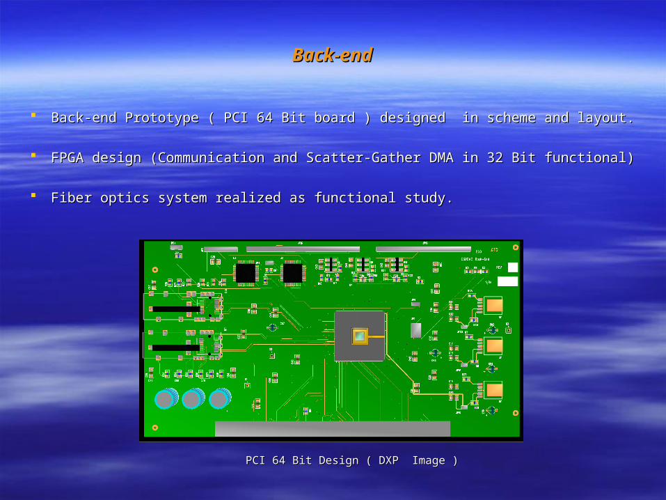
Back-end Prototype ( PCI 64 Bit board ) designed in scheme and layout. Back-end Prototype ( PCI 64 Bit board ) designed in scheme and layout.
FPGA design (Communication and Scatter-Gather DMA in 32 Bit functional)FPGA design (Communication and Scatter-Gather DMA in 32 Bit functional)
Fiber optics system realized as functional study.Fiber optics system realized as functional study.
PCI 64 Bit Design ( DXP Image )PCI 64 Bit Design ( DXP Image )

Front-endFront-end
Fiber optics system realized as functional study.Fiber optics system realized as functional study.
Sequencer realized as functional study.Sequencer realized as functional study.
Acquisition module ( Adc’s and preamp ) are already tested as a piggy-back Acquisition module ( Adc’s and preamp ) are already tested as a piggy-back back-up monolithic replacement for the Analogic hybrid ADC’s. Preamp will back-up monolithic replacement for the Analogic hybrid ADC’s. Preamp will have to be revised (single ended => symmetrical).have to be revised (single ended => symmetrical).
Clock driver could be realized like IRACE module – alternatives have to be Clock driver could be realized like IRACE module – alternatives have to be studied.studied.
If not implemented by high speed links : If not implemented by high speed links : Bus system mixture between IRACE ( daisy chain) and Compact PCI. Bus system mixture between IRACE ( daisy chain) and Compact PCI. Neither studies nor design.Neither studies nor design.
Power supply design not studied. Separate and remote from Front-end desired.Power supply design not studied. Separate and remote from Front-end desired.