Escape from an Optoelectronic Tweezer Trap: experimental results...
10
Escape from an optoelectronic tweezer trap: experimental results and simulations S HUAILONG Z HANG , 1,2,3,9 A DELE N IKITINA , 3 Y UJIE C HEN , 4 YANFENG Z HANG , 4 L IN L IU, 4 A NDREW G. F LOOD, 5 J OAN J UVERT, 6 M. D EAN C HAMBERLAIN , 1,2,3 N AZIR P. K HERANI , 5,7 S TEVEN L. N EALE , 8,10 AND A ARON R. WHEELER , 1,2,3,* 1 Donnelly Centre for Cellular and Biomolecular Research, 160 College Street, Toronto, M5S 3E1, Canada 2 Department of Chemistry, University of Toronto, 80 St George Street, Toronto, M5S 3H6, Canada 3 Institute of Biomaterials and Biomedical Engineering, 164 College Street, Toronto, M5S 3G9, Canada 4 State Key Laboratory of Optoelectronic Materials and Technologies, School of Electronics and Information Technology, Sun Yat-sen University, Guangzhou, 510275, China 5 Department of Electrical and Computer Engineering, University of Toronto, 10 King’s College Road, Toronto, M5S 3G4, Canada 6 Photonics Research Group, INTEC-Department, Ghent University-IMEC, Technologiepark-Zwijnaarde 15 iGent, 9052 Gent, Belgium 7 Department of Materials Science and Engineering, University of Toronto, 184 College Street, Toronto, M5S 3E4, Canada 8 School of Engineering, University of Glasgow, Glasgow, Scotland, G12 8LT, UK 9 [email protected] 10 [email protected] * [email protected] Abstract: Optoelectronic tweezers (OET) are a microsystem actuation technology capable of moving microparticles at mm s -1 velocities with nN forces. In this work, we analyze the behavior of particles manipulated by negative dielectrophoresis (DEP) forces in an OET trap. A user-friendly computer interface was developed to generate a circular rotating light pattern to control the movement of the particles, allowing their force profiles to be conveniently measured. Three-dimensional simulations were carried out to clarify the experimental results, and the DEP forces acting on the particles were simulated by integrating the Maxwell stress tensor. The simulations matched the experimental results and enabled the determination of a new “hopping” mechanism for particle-escape from the trap. As indicated by the simulations, there exists a vertical DEP force at the edge of the light pattern that pushes up particles to a region with a smaller horizontal DEP force. We propose that this phenomenon will be important to consider for the design of OET micromanipulation experiments for a wide range of applications. © 2018 Optical Society of America under the terms of the OSA Open Access Publishing Agreement OCIS codes: (350.4855) Optical tweezers or optical manipulation; (120.4880) Optomechanics; (120.4640) Optical instruments. References and links 1. P. Y. Chiou, A. T. Ohta, and M. C. Wu, “Massively parallel manipulation of single cells and microparticles using optical images,” Nature 436(7049), 370–372 (2005). 2. A. Jamshidi, S. L. Neale, K. Yu, P. J. Pauzauskie, P. J. Schuck, J. K. Valley, H. Y. Hsu, A. T. Ohta, and M. C. Wu, “Nanopen: Dynamic, Low-power, and Light-actuated Patterning of Nanoparticles,” Nano Lett. 9(8), 2921–2925 (2009). 3. H. Hwang and J. K. Park, “Optoelectrofluidic platforms for chemistry and biology,” Lab Chip 11(1), 33–47 (2011). 4. S. Xie, X. Wang, N. Jiao, S. Tung, and L. Liu, “Programmable micrometer-sized motor array based on live cells,” Lab Chip 17(12), 2046–2053 (2017). 5. A. T. Ohta, P. Y. Chiou, T. H. Han, J. C. Liao, U. Bhardwaj, E. R. B. McCabe, F. Yu, R. Sun, and M. C. Wu, “Dynamic cell and microparticle control via optoelectronic tweezers,” J. Microelectromech. Syst. 16(3), 491–499 (2007). 6. M. Woerdemann, C. Alpmann, M. Esseling, and C. Denz, “Advanced optical trapping by complex beam shaping,” Laser Photon. Rev. 7(6), 839–854 (2013). Vol. 26, No. 5 | 5 Mar 2018 | OPTICS EXPRESS 5300 #309982 https://doi.org/10.1364/OE.26.005317 Journal © 2018 Received 30 Oct 2017; revised 4 Jan 2018; accepted 5 Jan 2018; published 21 Feb 2018
Transcript of Escape from an Optoelectronic Tweezer Trap: experimental results...
Escape from an optoelectronic tweezer trap:experimental results and simulationsSHUAILONG ZHANG,1,2,3,9 ADELE NIKITINA,3 YUJIE CHEN,4
YANFENG ZHANG,4 LIN LIU,4 ANDREW G. FLOOD,5 JOAN JUVERT,6
M. DEAN CHAMBERLAIN,1,2,3 NAZIR P. KHERANI,5,7 STEVEN L.NEALE,8,10 AND AARON R. WHEELER,1,2,3,*
1Donnelly Centre for Cellular and Biomolecular Research, 160 College Street, Toronto, M5S 3E1, Canada2Department of Chemistry, University of Toronto, 80 St George Street, Toronto, M5S 3H6, Canada3Institute of Biomaterials and Biomedical Engineering, 164 College Street, Toronto, M5S 3G9, Canada4State Key Laboratory of Optoelectronic Materials and Technologies, School of Electronics andInformation Technology, Sun Yat-sen University, Guangzhou, 510275, China5Department of Electrical and Computer Engineering, University of Toronto, 10 King’s College Road,Toronto, M5S 3G4, Canada6Photonics Research Group, INTEC-Department, Ghent University-IMEC, Technologiepark-Zwijnaarde 15iGent, 9052 Gent, Belgium7Department of Materials Science and Engineering, University of Toronto, 184 College Street, Toronto,M5S 3E4, Canada8School of Engineering, University of Glasgow, Glasgow, Scotland, G12 8LT, [email protected]@glasgow.ac.uk* [email protected]
Abstract: Optoelectronic tweezers (OET) are a microsystem actuation technology capableof moving microparticles at mm s−1 velocities with nN forces. In this work, we analyze thebehavior of particles manipulated by negative dielectrophoresis (DEP) forces in an OET trap. Auser-friendly computer interface was developed to generate a circular rotating light pattern tocontrol the movement of the particles, allowing their force profiles to be conveniently measured.Three-dimensional simulations were carried out to clarify the experimental results, and theDEP forces acting on the particles were simulated by integrating the Maxwell stress tensor. Thesimulations matched the experimental results and enabled the determination of a new “hopping”mechanism for particle-escape from the trap. As indicated by the simulations, there exists avertical DEP force at the edge of the light pattern that pushes up particles to a region with asmaller horizontal DEP force. We propose that this phenomenon will be important to considerfor the design of OET micromanipulation experiments for a wide range of applications.© 2018 Optical Society of America under the terms of the OSA Open Access Publishing AgreementOCIS codes: (350.4855) Optical tweezers or optical manipulation; (120.4880) Optomechanics; (120.4640) Opticalinstruments.
References and links1. P. Y. Chiou, A. T. Ohta, and M. C. Wu, “Massively parallel manipulation of single cells and microparticles using
optical images,” Nature 436(7049), 370–372 (2005).2. A. Jamshidi, S. L. Neale, K. Yu, P. J. Pauzauskie, P. J. Schuck, J. K. Valley, H. Y. Hsu, A. T. Ohta, and M. C. Wu,
“Nanopen: Dynamic, Low-power, and Light-actuated Patterning of Nanoparticles,” Nano Lett. 9(8), 2921–2925(2009).
3. H. Hwang and J. K. Park, “Optoelectrofluidic platforms for chemistry and biology,” Lab Chip 11(1), 33–47 (2011).4. S. Xie, X. Wang, N. Jiao, S. Tung, and L. Liu, “Programmable micrometer-sized motor array based on live cells,”
Lab Chip 17(12), 2046–2053 (2017).5. A. T. Ohta, P. Y. Chiou, T. H. Han, J. C. Liao, U. Bhardwaj, E. R. B. McCabe, F. Yu, R. Sun, and M. C. Wu, “Dynamic
cell and microparticle control via optoelectronic tweezers,” J. Microelectromech. Syst. 16(3), 491–499 (2007).6. M. Woerdemann, C. Alpmann, M. Esseling, and C. Denz, “Advanced optical trapping by complex beam shaping,”
Laser Photon. Rev. 7(6), 839–854 (2013).
Vol. 26, No. 5 | 5 Mar 2018 | OPTICS EXPRESS 5300
#309982 https://doi.org/10.1364/OE.26.005317 Journal © 2018 Received 30 Oct 2017; revised 4 Jan 2018; accepted 5 Jan 2018; published 21 Feb 2018
7. S. L. Neale, M. Mazilu, J. I. B. Wilson, K. Dholakia, and T. F. Krauss, “The resolution of optical traps created bylight induced dielectrophoresis (LIDEP),” Opt. Exp. 15(20), 12619–12626 (2007).
8. A. Jamshidi, P. J. Pauzauskie, P. J. Schuck, A. T. Ohta, P. Y. Chiou, J. Chou, P. Yang, and M. C. Wu, “Dynamicmanipulation and separation of individual semiconducting and metallic nanowires,” Nat. Photon. 2(2), 86–89 (2008).
9. P. J. Pauzauskie, A. Jamshidi, J. K. Valley, J. H. Satcher Jr, and M. C. Wu, “Parallel trapping of multiwalled carbonnanotubes with optoelectronic tweezers,” Appl. Phys. Lett. 95(11), 113104 (2009).
10. S. M. Yang, T. M. Yu, H. P. Huang, M. Y. Ku, L. Hsu, and C. H. Liu, “Dynamic manipulation and patterning ofmicroparticles and cells by using TiOPc-based optoelectronic dielectrophoresis,” Opt. Lett. 35(12), 1959–1961(2010).
11. S. L. Neale, A. T. Ohta, H. Y. Hsu, J. K. Valley, A. Jamshidi, and M. C. Wu, “Trap profiles of projector basedoptoelectronic tweezers (OET) with HeLa cells,” Opt. Exp. 17(7), 5231–5239 (2009).
12. A. T. Ohta, M. Garcia, J. K. Valley, L. Banie, H.-Y. Hsu, A. Jamshidi, S. L. Neale, T. Lue, and M. C. Wu, “Motile andnon-motile sperm diagnostic manipulation using optoelectronic tweezers,” Lab Chip 10(23), 3213–3217 (2010).
13. G. B. Lee, C. J. Chang, C. H. Wang, M. Y. Lu, and Y. Y. Luo, “Continuous medium exchange and optically inducedelectroporation of cells in an integrated microfluidic system,” Microsyst. Nanoeng. 1, 15007 (2015).
14. S. Zhang, Y. Liu, J. Juvert, P. Tian, J. C. Navarro, J. M. Cooper, and S. L. Neale, “Use of optoelectronic tweezers inmanufacturing - accurate solder bead positioning,” Appl. Phys. Lett. 109(22), 221110 (2016).
15. Y. Yang, Y. Mao, K. S. Shin, C. O. Chui, and P. Y. Chiou, “Self-Locking Optoelectronic Tweezers for Single-Cell andMicroparticle Manipulation across a Large Area in High Conductivity Media,” Sci. Rep. 6, 22630 (2016).
16. J. Juvert, S. Zhang, I. Eddie, C. J. Mitchell, G. T. Reed, J. S. Wilkinson, A. Kelly, and S. L. Neale, “Micromanipulationof InP lasers with optoelectronic tweezers for integration on a photonic platform,” Opt. Exp. 24(16), 18163–18175(2016).
17. S. Zhang, J. Juvert, J. M. Cooper, and S. L. Neale, “Manipulating and assembling metallic beads with optoelectronictweezers,” Sci. Rep. 6, 32840 (2016).
18. S. Zhang, Y. Liu, Y. Qian, W. Li, J. Juvert, P. Tian, J. Navarro, A. W. Clark, E. Gu, M. D. Dawson, J. M. Cooper,and S. L. Neale, “Manufacturing with light - micro-assembly ofcopto-electronic microstructures,” Opt. Exp. 25(23),28838–28850 (2017).
19. S. Zhang, A. Nikitina, Y. Chen, Y. Zhang, L. Liu, A. G. Flood, J. Juvert, D. Chamberlain, N. P. Kherani, S. L. Neale, andA. R. Wheeler, “Carthwheel,” figshare (2017) [retrieved 24 Oct 2017], https://doi.org/10.6084/m9.figshare.5536627.
20. S. B. Huang, M. H. Wu, Y. H. Lin, C. H. Hsieh, C. L. Yang, H. C. Lin, C. P. Tseng, and G. B. Lee, “High-purityand labelfree isolation of circulating tumor cells (CTCs) in a microfluidic platform by using optically-induced-dielectrophoretic (ODEP) force,” Lab Chip 13(7), 1371–1383 (2013).
21. A. Zarowna-Dabrowska, S. L. Neale, D. Massoubre, J. McKendry, B. R. Rae, R. K. Henderson, M. J. Rose, H. Yin,J. M. Cooper, E. Gu, and M. M. Dawson, “Miniaturized optoelectronic tweezers controlled by GaN micro-pixel lightemitting diode arrays,” Opt. Exp. 19(3), 2720–2728 (2011).
22. R. Pethig, “Dielectrophoresis: Status of the theory, technology, and applications,” Biomicrofluidics 4(2), 022811(2010).
23. X. Wang, X. B. Wang, and P. R. C. Gascoyne, “General expressions for dielectrophoretic force and electrorotationaltorque derived using the Maxwell stress tensor method,” J. Electrostat. 39(4), 277–295 (1997).
24. S. Kumar and P. J. Hesketh, “Interpretation of ac dielectrophoretic behavior of tin oxide nanobelts using Maxwellstress tensor approach modeling,” Sensor Actuat. B Chem. 161(1), 1198–1208 (2012).
25. K. H. Kang, I. S. Kang, and C. M. Lee, “Wetting tension due to Coulombic interaction in charge-related wettingphenomena,” Langmuir 19(13), 5407–5412 (2003).
26. M. Abdelgawad, P. Park, and A. R. Wheeler, “Optimization of device geometry in single-plate digital microfluidics,”J. Appl. Phys. 105(9), 094506 (2009).
1. Introduction
Optoelectronic tweezers (OET) is an opto-electro-fluidic micromanipulation technology that useslight-induced dielectrophoresis (DEP) for touch-free actuation of micro-scale objects in physical,chemical and biomedical studies [1–5]. Compared to conventional optical tweezers, OET trapsexert a much stronger manipulation force for a given intensity of light, and in addition OET is wellsuited for massively parallel manipulation [1,6,7]. To date, there has been demonstration of OETmanipulation of many nano- and micro-scale objects, ranging from semiconductor nanowiresand carbon nanotubes [8, 9], to cells and particles on the order of tens of microns [10–15], tophotonic/electronic devices with sizes greater than 100 microns [16, 17].
OET has been reported to manipulate micro particles at velocities of several mm s−1 propelledby forces of up to nano-Newton levels [14, 17, 18]. This suggests utility for OET as a micro-assembly tool, making it important to characterize its effectiveness to manipulate targeted objectsin terms of the highest achievable positioning speed and accuracy. These properties are typically
Vol. 26, No. 5 | 5 Mar 2018 | OPTICS EXPRESS 5301
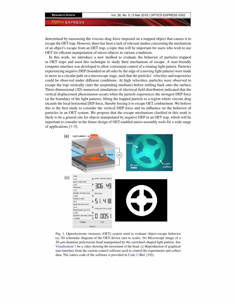
determined by measuring the viscous drag force imposed on a trapped object that causes it toescape the OET trap. However, there has been a lack of relevant studies concerning the mechanismof an object’s escape from an OET trap, a topic that will be important for users who wish to useOET for efficient manipulation of micro-objects in various conditions.In this work, we introduce a new method to evaluate the behavior of particles trapped
in OET traps and used this technique to study their mechanism of escape. A user-friendlycomputer interface was developed to allow convenient control of a rotating light pattern. Particlesexperiencing negative DEP (bounded on all sides by the edge of a moving light pattern) were madeto move in a circular path on a microscope stage, such that the particles’ velocities and trajectoriescould be observed under different conditions. At high velocities, particles were observed toescape the trap vertically (into the suspending medium) before settling back onto the surface.Three-dimensional (3D) numerical simulations of electrical field distribution indicated that thevertical displacement phenomenon occurs when the particle experiences the strongest DEP force(at the boundary of the light pattern), lifting the trapped particle to a region where viscous dragexceeds the local horizontal DEP force, thereby forcing it to escape OET confinement. We believethis is the first study to consider the vertical DEP force and its influence on the behavior ofparticles in an OET system. We propose that the escape mechanism clarified in this work islikely to be a general one for objects manipulated by negative DEP in an OET trap, which will beimportant to consider in the future design of OET-enabled micro-assembly tools for a wide rangeof applications [1–5].
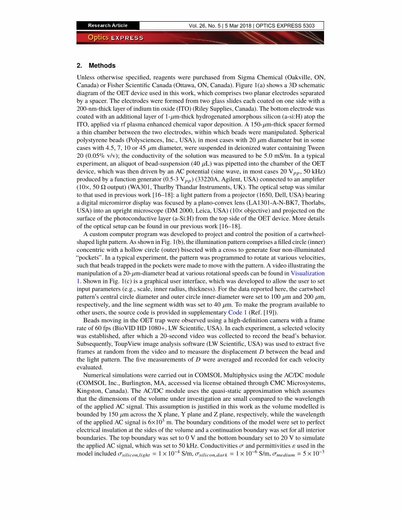
Fig. 1. Optoelectronic tweezers (OET) system used to evaluate object-escape behavior.(a) 3D schematic diagram of the OET device (not to scale). (b) Microscope image of a20-µm-diameter polystyrene bead manipulated by the cartwheel-shaped light pattern. SeeVisualization 1 for a video showing the movement of the bead. (c) Reproduction of graphicaluser-interface from the custom control software used to control the experiments and collectdata. The source code of the software is provided in Code 1 (Ref. [19]).
Vol. 26, No. 5 | 5 Mar 2018 | OPTICS EXPRESS 5302
2. Methods
Unless otherwise specified, reagents were purchased from Sigma Chemical (Oakville, ON,Canada) or Fisher Scientific Canada (Ottawa, ON, Canada). Figure 1(a) shows a 3D schematicdiagram of the OET device used in this work, which comprises two planar electrodes separatedby a spacer. The electrodes were formed from two glass slides each coated on one side with a200-nm-thick layer of indium tin oxide (ITO) (Riley Supplies, Canada). The bottom electrode wascoated with an additional layer of 1-µm-thick hydrogenated amorphous silicon (a-si:H) atop theITO, applied via rf plasma enhanced chemical vapor deposition. A 150-µm-thick spacer formeda thin chamber between the two electrodes, within which beads were manipulated. Sphericalpolystyrene beads (Polysciences, Inc., USA), in most cases with 20 µm diameter but in somecases with 4.5, 7, 10 or 45 µm diameter, were suspended in deionized water containing Tween20 (0.05% v/v); the conductivity of the solution was measured to be 5.0 mS/m. In a typicalexperiment, an aliquot of bead-suspension (40 µL) was pipetted into the chamber of the OETdevice, which was then driven by an AC potential (sine wave, in most cases 20 Vpp, 50 kHz)produced by a function generator (0.5-3 Vpp) (33220A, Agilent, USA) connected to an amplifier(10×, 50 Ω output) (WA301, Thurlby Thandar Instruments, UK). The optical setup was similarto that used in previous work [16–18]: a light pattern from a projector (1650, Dell, USA) bearinga digital micromirror display was focused by a plano-convex lens (LA1301-A-N-BK7, Thorlabs,USA) into an upright microscope (DM 2000, Leica, USA) (10× objective) and projected on thesurface of the photoconductive layer (a-Si:H) from the top side of the OET device. More detailsof the optical setup can be found in our previous work [16–18].
A custom computer program was developed to project and control the position of a cartwheel-shaped light pattern. As shown in Fig. 1(b), the illumination pattern comprises a filled circle (inner)concentric with a hollow circle (outer) bisected with a cross to generate four non-illuminated“pockets”. In a typical experiment, the pattern was programmed to rotate at various velocities,such that beads trapped in the pockets were made to move with the pattern. A video illustrating themanipulation of a 20-µm-diameter bead at various rotational speeds can be found in Visualization1. Shown in Fig. 1(c) is a graphical user interface, which was developed to allow the user to setinput parameters (e.g., scale, inner radius, thickness). For the data reported here, the cartwheelpattern’s central circle diameter and outer circle inner-diameter were set to 100 µm and 200 µm,respectively, and the line segment width was set to 40 µm. To make the program available toother users, the source code is provided in supplementary Code 1 (Ref. [19]).Beads moving in the OET trap were observed using a high-definition camera with a frame
rate of 60 fps (BioVID HD 1080+, LW Scientific, USA). In each experiment, a selected velocitywas established, after which a 20-second video was collected to record the bead’s behavior.Subsequently, ToupView image analysis software (LW Scientific, USA) was used to extract fiveframes at random from the video and to measure the displacement D between the bead andthe light pattern. The five measurements of D were averaged and recorded for each velocityevaluated.
Numerical simulations were carried out in COMSOL Multiphysics using the AC/DC module(COMSOL Inc., Burlington, MA, accessed via license obtained through CMC Microsystems,Kingston, Canada). The AC/DC module uses the quasi-static approximation which assumesthat the dimensions of the volume under investigation are small compared to the wavelengthof the applied AC signal. This assumption is justified in this work as the volume modelled isbounded by 150 µm across the X plane, Y plane and Z plane, respectively, while the wavelengthof the applied AC signal is 6×10³ m. The boundary conditions of the model were set to perfectelectrical insulation at the sides of the volume and a continuation boundary was set for all interiorboundaries. The top boundary was set to 0 V and the bottom boundary set to 20 V to simulatethe applied AC signal, which was set to 50 kHz. Conductivities σ and permittivities ε used in themodel included σsilicon,light = 1× 10⁻⁴ S/m, σsilicon,dark = 1× 10⁻⁶ S/m, σmedium = 5× 10⁻³
Vol. 26, No. 5 | 5 Mar 2018 | OPTICS EXPRESS 5303
S/m, εmedium = 80, σbead = 1 × 10⁻¹⁴ S/m, and εmedium = 2.4. Finally, the model employed afree tetrahedral mesh with a minimum element size of 0.227 µm, a maximum element size of5.29 µm, an element growth rate of 1.35, a resolution of curvature of 0.3, and a resolution ofnarrow regions of 0.85.
3. Experimental results and discussion
OET traps used to manipulate particles often rely on negative DEP - that is, a “pocket” of light isprojected to surround the particle, and the negative DEP forces cause the particle to remain inthe pocket as the light pattern is moved [1, 4, 5, 11, 12]. Previous approaches to evaluating OETobject-trapping force in such cases have involved moving either the OET trap or a microscopestage linearly [11, 14, 17] at different velocities. These systems are not ideal, as the large workingarea results in frequent experimental interruptions caused by collisions between the trappedbead and debris or other beads. To overcome this challenge, we developed a system in which acartwheel-shaped light pattern (bearing four “pockets” or traps) is rotated at different frequencies,as shown in Fig. 1. The linear velocity of a bead trapped in this rotating system is easily determinedfrom the angular velocity of the light pattern and the center-to-center distance between thebead and the light pattern can be observed in images collected with a camera. In this work, theReynolds number for a 20-µm-diameter bead moving at a maximum linear velocity of 340 µm/sis 0.0082, suggesting that the system is in the laminar flow regime, verifying two experimentalassumptions. First, the low inertial forces allow the estimation of DEP force responsible for beadmotion to be equivalent to the viscous drag force, which is given by Stoke’s law [7, 11, 14]:
FDEP = Fdrag (1)
Fdrag = 6πηrν (2)
where η is the viscosity of the liquid, r is the radius of the bead and ν is velocity of the bead. Sincein these experiments gravity forces the bead to settle in proximity to the device surface, Faxen’scorrection based on the radius of the microsphere (10 µm) was used to adjust the calculation ofviscous drag force and DEP force [7, 14, 17, 20]. Second, the low inertial forces justify the use ofa rotary particle movement path, noting that in a high Reynolds number environment, the particlewould be continually accelerating against its inertia but the low Reynold’s number system can beapproximated as producing a continuous linear velocity.
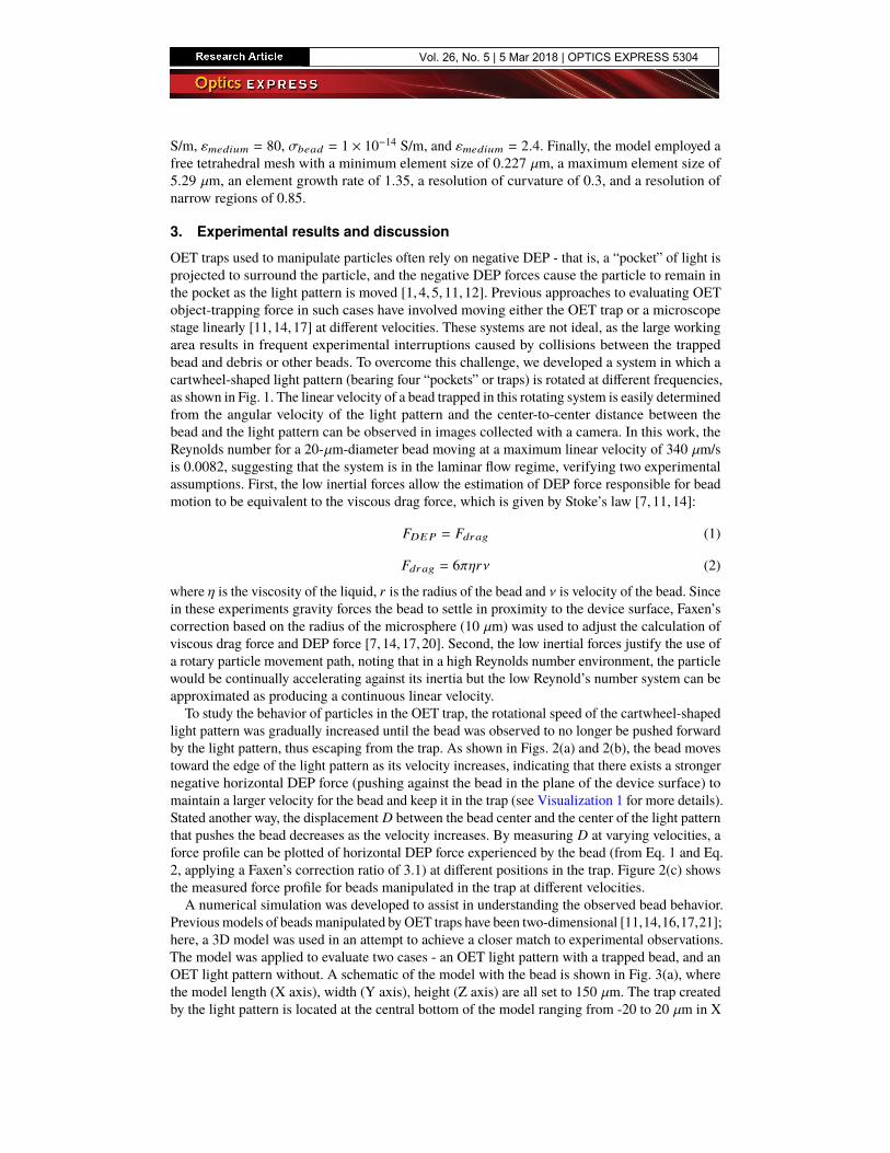
To study the behavior of particles in the OET trap, the rotational speed of the cartwheel-shapedlight pattern was gradually increased until the bead was observed to no longer be pushed forwardby the light pattern, thus escaping from the trap. As shown in Figs. 2(a) and 2(b), the bead movestoward the edge of the light pattern as its velocity increases, indicating that there exists a strongernegative horizontal DEP force (pushing against the bead in the plane of the device surface) tomaintain a larger velocity for the bead and keep it in the trap (see Visualization 1 for more details).Stated another way, the displacement D between the bead center and the center of the light patternthat pushes the bead decreases as the velocity increases. By measuring D at varying velocities, aforce profile can be plotted of horizontal DEP force experienced by the bead (from Eq. 1 and Eq.2, applying a Faxen’s correction ratio of 3.1) at different positions in the trap. Figure 2(c) showsthe measured force profile for beads manipulated in the trap at different velocities.
A numerical simulation was developed to assist in understanding the observed bead behavior.Previousmodels of beadsmanipulated byOET traps have been two-dimensional [11,14,16,17,21];here, a 3D model was used in an attempt to achieve a closer match to experimental observations.The model was applied to evaluate two cases - an OET light pattern with a trapped bead, and anOET light pattern without. A schematic of the model with the bead is shown in Fig. 3(a), wherethe model length (X axis), width (Y axis), height (Z axis) are all set to 150 µm. The trap createdby the light pattern is located at the central bottom of the model ranging from -20 to 20 µm in X
Vol. 26, No. 5 | 5 Mar 2018 | OPTICS EXPRESS 5304
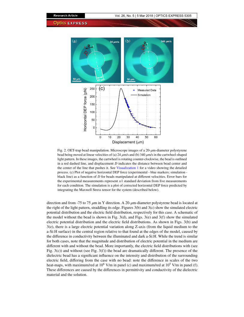
Fig. 2. OET-trap bead manipulation. Microscope images of a 20-µm-diameter polystyrenebead being moved at linear velocities of (a) 24 µm/s and (b) 340 µm/s in the cartwheel-shapedlight pattern. In these images, the cartwheel is rotating counter-clockwise, the bead is outlinedin a red dashed line, and displacement D indicates the distance between bead center andthe center of the line that pushes it. See Visualization 1 for a video showing the detailedprocess. (c) Plot of negative horizontal DEP force (experimental - blue markers; simulation -black line) as a function of D for beads manipulated at different velocities. Error bars forthe experimental measurements represent ±1 standard deviation from five measurementsfor each condition. The simulation is a plot of corrected horizontal DEP force predicted byintegrating the Maxwell Stress tensor for the system (described below).
direction and from -75 to 75 µm in Y direction. A 20-µm-diameter polystyrene bead is located atthe right of the light pattern, straddling its edge. Figures 3(b) and 3(c) show the simulated electricpotential distribution and the electric field distribution, respectively for this case. A schematic ofthe model without the bead is shown in Fig. 3(d), and Figs. 3(e) and 3(f) show the simulatedelectric potential distribution and the electric field distributions. As shown in Figs. 3(b) and3(e), there is a large electric potential variation along Z-axis (from the liquid medium to thea-Si:H surface) in the central region relative to that found at the edges of the model, caused bythe difference in conductivity between the illuminated and dark a-Si:H. While the trend is similarfor both cases, note that the magnitude and distribution of electric potential in the medium aredifferent with and without the bead. More importantly, the electric field distributions with (seeFig. 3(c)) and without (see Fig. 3(f)) the bead are dramatically different. The presence of thedielectric bead has a significant influence on the intensity and distribution of the surroundingelectric field, differing from the case with no bead: note the difference in scales of the twoheat-maps, with maximum/red at 106 V/m in panel (c) and maximum/red at 105 V/m in panel (f).These differences are caused by the differences in permittivity and conductivity of the dielectricmaterial and the solution.
Vol. 26, No. 5 | 5 Mar 2018 | OPTICS EXPRESS 5305
Fig. 3. 3D numerical simulations of the OET trap. (a,d) Schematics and plots of simulatedelectric potential (b,e) and electric field (c,f) for an OET trap formed by illuminating a40-µm-wide light pattern (shaded in green) with (a-c) or without (d-f) a 20-µm-diameterpolystyrene bead straddling the edge of the light pattern. Z-X cut planes in (a,d) form thebasis for the plots in (b-f), in which the simulated electric potential and field are indicated inheat maps (blue = low, red - high). In (b,c), the bead is illustrated as an open black circle. In(c,f), the insets are a magnified portion of the 1 µm × 3 µm (Z × X) region encompassingthe edge of the light pattern.
With the simulations of electric potential and field, we turned our attention to simulating thebehavior of DEP force acting on the bead. DEP force is typically calculated using a classic dipoleapproximation method [22] in which the force acting on a spherical particle is expressed as:
FDEP = 2πr3εmRe [K (ω)] ∇E2 (3)
where r is the radius of the particle, εm is the permittivity of the medium, Re [K (ω)] is the realcomponent of the Clausius-Mossotti (CM) factor (which is dependent on angular frequencyω), and ∇E2 is the gradient of the external electric field’s square. This dipole approximationmethod is useful for qualitatively indicating whether positive or negative DEP is expectedfor particular material and fluid combinations, and in predicting the DEP trends for simplegeometric arrangements. However, this approximation is strictly applicable only when the particleis much smaller than the scale of the field non-uniformity (and thus has little influence on thenon-uniformity of the surrounding electric field [22]). As shown in Figs. 3(c) and 3(f), thatcriterion does not apply to the system described here.
With the limitations of Eq. 3 in mind, a second model of DEP force based on the integration ofMaxwell stress tensor was used here. This method, which has been used previously to calculateDEP forces [16, 23, 24] as well as forces acting on droplets in digital microfluidics [25, 26], isderived from the Lorentz force law and can be expressed as:
σi j = ε0EiEj +1µ 0
BiBj −12
(ε0E2 +
1µ 0
B2)δi j (4)
where σi j is the i j element of the second rankMaxwell stress tensor, ε0 is the vacuum permittivity,µ0 is the vacuum permeability, E and B are the electric and magnetic fields, respectively, and δi j
Vol. 26, No. 5 | 5 Mar 2018 | OPTICS EXPRESS 5306
is Kronecker’s delta. The element σi j of the Maxwell stress tensor has a unit of force per unitarea, and the i j element of the tensor can also be interpreted as the force per unit area parallelto the th ith axis crossing a surface normal to the jth axis. The diagonal elements represent thepulling forces while the off-diagonal elements represent the shear stress [16, 23]. Therefore, thetotal force acting on a volume of dielectric inside an electromagnetic field can be calculated byintegrating the Maxwell stress tensor of the electromagnetic field over the surface area of thevolume,
FDEP =
∮s
σ · ndS (5)
where S represents the surface enclosing the bead and n represents the unit vector.Using Eq. 5, we simulated the negative horizontal DEP force acting on beads with different
displacement D for the model in Fig. 3(a) (assuming a Z-dimension position of the bead of 100nm above the a-Si:H surface). The simulated horizontal DEP forces were found to be stronger thanthe measured forces in this system, suggesting that the beads used in experiments may experiencegreater frictional forces than predicted (including interactions with the surface). Additionally, thesimulation assumes that some electrical potential is lost on contact resistance and thus does notdrop across the liquid layer; experimentally this assumption may not hold true. Nevertheless,after scaling the simulation result by a factor of 0.43, there is a good match between the simulated(solid line) and measured (blue markers) results in Fig. 2(c). Further, the simulated negativehorizontal force profile has a peak at the edge of the light pattern, which matches the experimentalresult that the bead experiences a stronger horizontal DEP force at the edge of the light pattern.An interesting phenomenon was also observed from the simulation and experimental results:in experiments, the bead escapes the trap prior to experiencing the maximum horizontal DEPforce. Based on the simulation, the bead should experience a maximum horizontal DEP force ofroughly 253 pN, with a displacement of 22 µm. However, in experiments, beads were alwaysobserved to escape the trap at (or before) reaching a displacement of 26.5 µm (which, accordingto the simulation, represents a horizontal DEP force of 189 pN). Note that this behavior is quitedifferent from a particle moving under positive DEP in an OET system, in which trapped particlesalways reach maximum displacement and DEP force before escaping the trap [14, 17]. Since thehorizontal DEP force balances the viscous drag force and keeps the bead in the trap, our initialhypothesis was that beads would escape the trap when the DEP force reaches its maximum andcan no longer increase to match the viscous drag force.
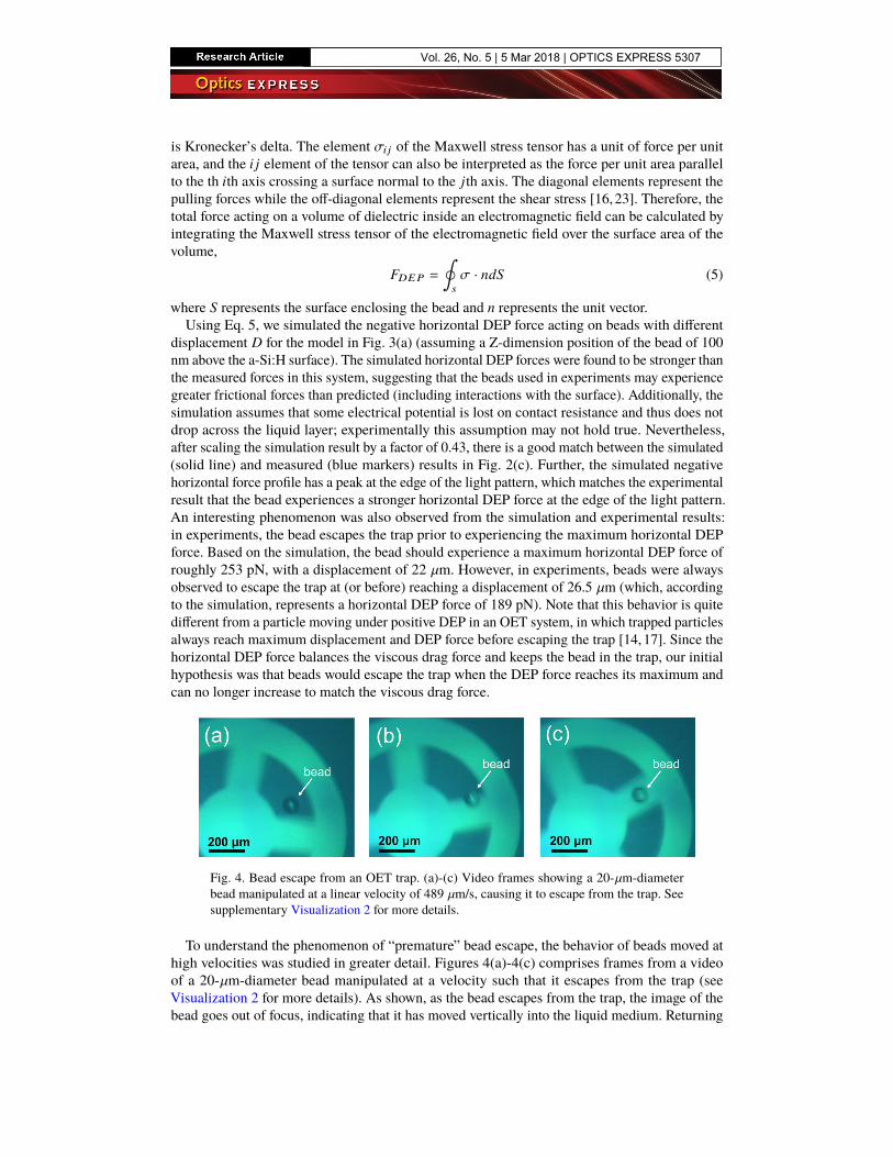
Fig. 4. Bead escape from an OET trap. (a)-(c) Video frames showing a 20-µm-diameterbead manipulated at a linear velocity of 489 µm/s, causing it to escape from the trap. Seesupplementary Visualization 2 for more details.
To understand the phenomenon of “premature” bead escape, the behavior of beads moved athigh velocities was studied in greater detail. Figures 4(a)-4(c) comprises frames from a videoof a 20-µm-diameter bead manipulated at a velocity such that it escapes from the trap (seeVisualization 2 for more details). As shown, as the bead escapes from the trap, the image of thebead goes out of focus, indicating that it has moved vertically into the liquid medium. Returning
Vol. 26, No. 5 | 5 Mar 2018 | OPTICS EXPRESS 5307
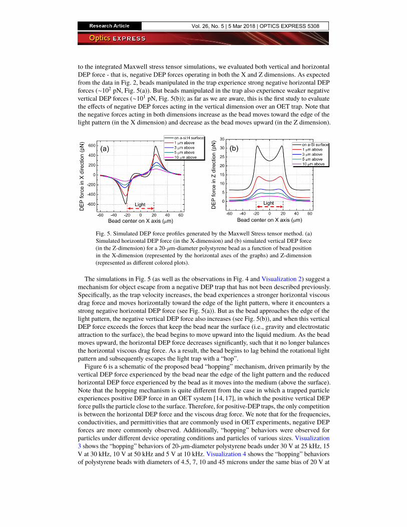
to the integrated Maxwell stress tensor simulations, we evaluated both vertical and horizontalDEP force - that is, negative DEP forces operating in both the X and Z dimensions. As expectedfrom the data in Fig. 2, beads manipulated in the trap experience strong negative horizontal DEPforces (∼102 pN, Fig. 5(a)). But beads manipulated in the trap also experience weaker negativevertical DEP forces (∼101 pN, Fig. 5(b)); as far as we are aware, this is the first study to evaluatethe effects of negative DEP forces acting in the vertical dimension over an OET trap. Note thatthe negative forces acting in both dimensions increase as the bead moves toward the edge of thelight pattern (in the X dimension) and decrease as the bead moves upward (in the Z dimension).
Fig. 5. Simulated DEP force profiles generated by the Maxwell Stress tensor method. (a)Simulated horizontal DEP force (in the X-dimension) and (b) simulated vertical DEP force(in the Z-dimension) for a 20-µm-diameter polystyrene bead as a function of bead positionin the X-dimension (represented by the horizontal axes of the graphs) and Z-dimension(represented as different colored plots).
The simulations in Fig. 5 (as well as the observations in Fig. 4 and Visualization 2) suggest amechanism for object escape from a negative DEP trap that has not been described previously.Specifically, as the trap velocity increases, the bead experiences a stronger horizontal viscousdrag force and moves horizontally toward the edge of the light pattern, where it encounters astrong negative horizontal DEP force (see Fig. 5(a)). But as the bead approaches the edge of thelight pattern, the negative vertical DEP force also increases (see Fig. 5(b)), and when this verticalDEP force exceeds the forces that keep the bead near the surface (i.e., gravity and electrostaticattraction to the surface), the bead begins to move upward into the liquid medium. As the beadmoves upward, the horizontal DEP force decreases significantly, such that it no longer balancesthe horizontal viscous drag force. As a result, the bead begins to lag behind the rotational lightpattern and subsequently escapes the light trap with a “hop”.Figure 6 is a schematic of the proposed bead “hopping” mechanism, driven primarily by the
vertical DEP force experienced by the bead near the edge of the light pattern and the reducedhorizontal DEP force experienced by the bead as it moves into the medium (above the surface).Note that the hopping mechanism is quite different from the case in which a trapped particleexperiences positive DEP force in an OET system [14,17], in which the positive vertical DEPforce pulls the particle close to the surface. Therefore, for positive-DEP traps, the only competitionis between the horizontal DEP force and the viscous drag force. We note that for the frequencies,conductivities, and permittivities that are commonly used in OET experiments, negative DEPforces are more commonly observed. Additionally, “hopping” behaviors were observed forparticles under different device operating conditions and particles of various sizes. Visualization3 shows the “hopping” behaviors of 20-µm-diameter polystyrene beads under 30 V at 25 kHz, 15V at 30 kHz, 10 V at 50 kHz and 5 V at 10 kHz. Visualization 4 shows the “hopping” behaviorsof polystyrene beads with diameters of 4.5, 7, 10 and 45 microns under the same bias of 20 V at
Vol. 26, No. 5 | 5 Mar 2018 | OPTICS EXPRESS 5308
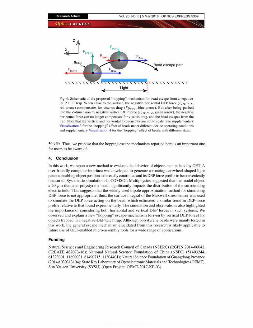
Fig. 6. Schematic of the proposed “hopping” mechanism for bead escape from a negative-DEP OET trap. When close to the surface, the negative horizontal DEP force (FDEP−X ,red arrow) compensates for viscous drag (FDrag, blue arrow). But after being pushedinto the Z-dimension by negative vertical DEP force (FDEP−Z , green arrow), the negativehorizontal force can no longer compensate for viscous drag, and the bead escapes from thetrap. Note that the vertical and horizontal force-arrows are not to scale. See supplementaryVisualization 3 for the “hopping” effect of beads under different device operating conditionsand supplementary Visualization 4 for the “hopping” effect of beads with different sizes.
50 kHz. Thus, we propose that the hopping escape mechanism reported here is an important onefor users to be aware of.
4. Conclusion
In this work, we report a new method to evaluate the behavior of objects manipulated by OET. Auser-friendly computer interface was developed to generate a rotating cartwheel-shaped lightpattern, enabling object position to be easily controlled and its DEP force profile to be convenientlymeasured. Systematic simulations in COMSOL Multiphysics suggested that the model object,a 20-µm-diameter polystyrene bead, significantly impacts the distribution of the surroundingelectric field. This suggests that the widely used dipole approximation method for simulatingDEP force is not appropriate; thus, the surface integral of the Maxwell stress tensor was usedto simulate the DEP force acting on the bead, which estimated a similar trend in DEP-forceprofile relative to that found experimentally. The simulation and observations also highlightedthe importance of considering both horizontal and vertical DEP forces in such systems. Weobserved and explain a new “hopping” escape-mechanism (driven by vertical DEP force) forobjects trapped in a negative-DEP OET trap. Although polystyrene beads were mainly tested inthis work, the general escape mechanism elucidated from this research is likely applicable tofuture use of OET-enabled micro-assembly tools for a wide range of applications.
Funding
Natural Sciences and Engineering Research Council of Canada (NSERC) (RGPIN 2014-06042,CREATE 482073-16); National Natural Science Foundation of China (NSFC) (51403244,61323001, 11690031, 61490715, 11304401); Natural Science Foundation of Guangdong Province(2014A030313104); State Key Laboratory of OptoelectronicMaterials and Technologies (OEMT),Sun Yat-sen University (SYSU) (Open Project: OEMT-2017-KF-03).
Vol. 26, No. 5 | 5 Mar 2018 | OPTICS EXPRESS 5309