
Error Handling and Energy Estimation Framework For Error ...
175
HAL Id: tel-01636803 https://hal.inria.fr/tel-01636803 Submitted on 17 Nov 2017 HAL is a multi-disciplinary open access archive for the deposit and dissemination of sci- entific research documents, whether they are pub- lished or not. The documents may come from teaching and research institutions in France or abroad, or from public or private research centers. L’archive ouverte pluridisciplinaire HAL, est destinée au dépôt et à la diffusion de documents scientifiques de niveau recherche, publiés ou non, émanant des établissements d’enseignement et de recherche français ou étrangers, des laboratoires publics ou privés. Error Handling and Energy Estimation Framework For Error Resilient Near-Threshold Computing Rengarajan Ragavan To cite this version: Rengarajan Ragavan. Error Handling and Energy Estimation Framework For Error Resilient Near- Threshold Computing. Embedded Systems. Rennes 1, 2017. English. tel-01636803
Transcript of Error Handling and Energy Estimation Framework For Error ...
HAL Id: tel-01636803https://hal.inria.fr/tel-01636803
Submitted on 17 Nov 2017
HAL is a multi-disciplinary open accessarchive for the deposit and dissemination of sci-entific research documents, whether they are pub-lished or not. The documents may come fromteaching and research institutions in France orabroad, or from public or private research centers.
L’archive ouverte pluridisciplinaire HAL, estdestinée au dépôt et à la diffusion de documentsscientifiques de niveau recherche, publiés ou non,émanant des établissements d’enseignement et derecherche français ou étrangers, des laboratoirespublics ou privés.
Error Handling and Energy Estimation Framework ForError Resilient Near-Threshold Computing
Rengarajan Ragavan
To cite this version:Rengarajan Ragavan. Error Handling and Energy Estimation Framework For Error Resilient Near-Threshold Computing. Embedded Systems. Rennes 1, 2017. English. �tel-01636803�
No d’ordre : ANNÉE 2017
THÈSE / UNIVERSITÉ DE RENNES 1sous le sceau de l’Université Bretagne Loire
pour le grade deDOCTEUR DE L’UNIVERSITÉ DE RENNES 1
Mention : Traitement du Signal et TélécommunicationsÉcole doctorale MATISSE
présentée par
Rengarajan RAGAVANpréparée à l’unité de recherche UMR6074 IRISA
Institut de recherche en informatique et systèmes aléatoires - CAIRNÉcole Nationale Supérieure des Sciences Appliquées et de Technologie
Error Handling and
Energy Estimation
Framework ForError ResilientNear-ThresholdComputing
Thèse soutenue à Lannionle 22 septembre 2017
devant le jury composé de :
Edith BEIGNÉDirectrice de Recherche à CEA Leti / rapporteur
Patrick GIRARDDirectrice de Recherche à CNRS, LIRMM / rappor-teur
Lorena ANGHELProfesseur à Grenoble INP, TIMA / examinateur
Daniel MÉNARDProfesseur à INSA Rennes, IETR / examinateur
Olivier SENTIEYSProfesseur à l’Université de Rennes 1 / directeur dethèse
Cédric KILLIANMaître de Conférences à l’Université de Rennes 1 /co-directeur de thèse


To My Parents, My Brother, and My Teachers
iii


Acknowledgements
I sincerely express my gratitude to my thesis supervisor Prof. Olivier Sentieys who
gave me the opportunity to work him in prestigious INRIA/IRISA labs. His guidance
and confidence in me gave extra boost and cultivated more interest in me to do this
research work in a better way. His feedback and comments refined the quality of my
research contributions and this thesis dissertation.
I am very grateful to my thesis co-supervisor Dr. Cedric Killian for his encour-
agement and support. He was inspirational to me throughout my Ph.D. tenure. His
suggestions and critical evaluation helped me to innovatively address various bottlenecks
in this thesis work. I register my special thanks to Cedric for his efforts in translating
the long abstract of this thesis to French.
I would like to thank my colleague Philippe Quemerais, Research Engineer, IRISA
labs for his extensive support in configuring and tutoring various CAD tools. I acknowl-
edge my fellow research student Benjamin Barrois for his help in modelling approximate
arithmetic operators.
I’m thankful to Mme. Laurence Gallas for her French lessons that helped me a
lot during my stay in Lannion. Also, I would like to thank all the faculty members,
researchers, and colleagues of ENSSAT who made my stay in Lannion most cherishable.
This thesis work has seen the light of the day thanks to Universite de Rennes 1,
and IRISA laboratory for funding and facilitating this thesis work. Thanks are due to
Nadia, Joelle, and Angelique for their support in administrative matters and during my
missions abroad.
I also express my gratitude to the entire jury panel for reading my thesis dissertation
and taking part in the thesis defense. Also, special thanks to the reviewers for their
valuable review comments that improved the quality of this dissertation.
I offer my sincere thanks to all my friends and well-wishers who were supporting
me all these years and looking for my betterment. Last but not least, I express my
everlasting gratitude to my parents, my brother and almighty without them I cannot be
what I am today.
10th October 2017 Rengarajan
Lannion, France
v


Abstract
Advancement in CMOS IC technology has improved the way in which integrated circuits
are designed and fabricated over decades. Scaling down the size of transistors from
micrometers to few nanometers has given the capability to place more tinier transistors
in a unit of chip area that upheld Moore’s law over the years. On the other hand,
feature size scaling imposed various challenges like physical, material, power-thermal,
technological, and economical that hinder the trend of scaling. To improve energy
efficiency, Dynamic Voltage Scaling (DVS) is employed in most of the Ultra-Low Power
(ULP) designs. In near-threshold region (NTR), the supply voltage of the transistor is
slightly more than the threshold voltage of the transistor. In this region, the delay and
energy both are roughly linear with the supply voltage. The Ion/Ioff ratio is higher
compared to the sub-threshold region, which improves the speed and minimizes the
leakage. Due to the reduced supply voltage, the circuits operating in NTR can achieve
a 10× reduction in energy per operation at the cost of the same magnitude of reduction
in the operating frequency. In the present trend of sub-nanometer designs, inherent
low-leakage technologies like FD-SOI (Fully Depleted Silicon On Insulator), enhance the
benefits of voltage scaling by utilizing techniques like Back-Biasing. However reduction
in Vdd augments the impact of variability and timing errors in sub-nanometer designs.
The main objective of this work is to handle timing errors and to formulate a
framework to estimate energy consumption of error resilient applications in the context
of near-threshold computing. It is highly beneficial to design a digital system by taking
advantage of NTR, DVS, and FD-SOI. In spite of the advantages, the impact of vari-
ability and timing errors outweighs the above-mentioned benefits. There are existing
methods that can predict and prevent errors, or detect and correct errors. But there is
a need for a unified approach to handle timing errors in the near-threshold regime.
In this thesis, Dynamic Speculation based error detection and correction is explored
in the context of adaptive voltage and clock overscaling. Apart from error detection
and correction, some errors can also be tolerated or, in other words, circuits can be
pushed beyond their limits to compute incorrectly to achieve higher energy efficiency.
The proposed error detection and correction method achieves 71% overclocking with 2%
additional hardware cost. This work involves extensive study of design at gate level to
understand the behaviour of gates under overscaling of supply voltage, bias voltage and
clock frequency (collectively called as operating triads). A bottom-up approach is taken:
by studying trends of energy vs. error of basic arithmetic operators at transistor level.
Based on profiling of the arithmetic operators, a tool flow is formulated to estimate
energy and error metrics for different operating triads. We achieve maximum energy
efficiency of 89% for arithmetic operators like 8-bit and 16-bit adders at the cost of 20%

faulty bits by operating in NTR. A statistical model is developed for the arithmetic
operators to represent the behaviour of the operators for different variability impacts.
This model is used for approximate computing of error resilient applications that can
tolerate acceptable margin of errors. This method is further explored for execution unit
of a VLIW processor. The proposed framework provides a quick estimation of energy
and error metrics of benchmark programs by simple compilation in using C compiler.
In the proposed energy estimation framework, characterization of arithmetic operators
is done at transistor level, and the energy estimation is done at functional level. This
hybrid approach makes energy estimation faster and accurate for different operating
triads. The proposed framework estimates energy for different benchmark programs
with 98% accuracy compared to SPICE simulation.

Abbreviations
AVS Adaptive Voltage sscaling
BER Bit Error Rate
BKA Brent-Kung Adder
BOX Buried OXide
CCS Conditional Carry Select
CDM Critical Delay Margin
CGRA Coarse-Grained Reconfigurable Architecture
CMF Common Mode Failure
CMOS Complementary Metal-Oxide-Semiconductor
DDMR Diverse Double Modular Redundancy
DMR Double Modular Redundancy
DSP Digital Signal Processor
DVFS Dynamic Voltage Frequency sscaling
DVS Dynamic Voltage sscaling
EDAP Energy Delay Area Product
EDP Energy Delay Product
FBB Forward Body Biasing
FEHM Flexible Error Handling Module
FF Flip-Flop
FIR Finite Impulse Response
FPGA Field-Programming Gate Array
FDSOI Fully Depleted Silicon on Insulator
FU Functional Unit
GRAAL Global Reliability Architecture Approach for Logic
HFM High Frequency Mode
ix

HPM Hardware Herformance Monitor
IC Integrated Chip
ILA Integrated Logic Analyzer
ILEP Instruction Level Power Estimation
ILP Instruction Level Parallelism
IoT Internet of Things
ISA Instruction Set Architecture
LFBFF Linear Feed Back Flip Flop
LFM Low Frequency Mode
LFSR Linear Feedbacl Shift Register
LSB Least Significant Bit
LUT Look-Up Table
LVDS Low-Voltage Differential Signaling
LVT Low VT
MMCM Mixed Mode Clock Manager
MSB Most Significant Bit
MSFF Master Slave Flip Flop
NOP No OPeration
NTR Near-Threshold Region
PE Processing Element
POFF Point of First Failure
PUM Path Under Monitoring
RBB Reverse Body Biasing
RCA Ripple Carry Adder
RTL Resistor- Transistor Logic
RVT Regular VT
SET Single Event Transients
SEU Single Event Upset
SNR Signal to Noise Ratio
SNW Single N-Well
SOI Silicon on Insulator
SPICE Simulation Program with Integrated Circuit Emphasis
SPW Single P-Well

STA Static Timing Analysis
STR Sub-Threshold Region
SW Single Well
TFD Timing Fault Detector
TMR Triple Modular Redundancy
UTBB Ultra-Thin Body and Box
VEX ISA VEX Instruction Set Architecture
VLIW Very Large Instruction Word
VOS Voltage Over-Scaling

Contents
Acknowledgements v
Abstract vii
Abbreviations ix
Contents 1
List of Figures 5
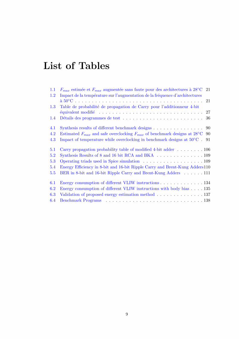
List of Tables 9
1 Resume etendu 11
1.1 Introduction . . . . . . . . . . . . . . . . . . . . . . . . . . . . . . . . . . . 11
1.2 Contributions . . . . . . . . . . . . . . . . . . . . . . . . . . . . . . . . . . 13
1.3 Gestion des erreurs temporelles . . . . . . . . . . . . . . . . . . . . . . . . 14
1.3.1 Gestion des erreurs avec une fenetre de speculation dynamique . . 15
1.3.2 Boucle de retour pour augmentation ou diminution de la frequence 17
1.3.3 Validation du concept sur FPGA Virtex de Xilinx . . . . . . . . . 18
1.4 Ajustement agressif de l’alimentation pour les applications resistantes auxerreurs . . . . . . . . . . . . . . . . . . . . . . . . . . . . . . . . . . . . . . 23
1.4.1 Modelisation d’operateur arithmetique avec gestion agressive dela tension d’alimentation . . . . . . . . . . . . . . . . . . . . . . . . 24
1.4.2 Validation du concept: modelisation d’additionneurs . . . . . . . . 25
1.5 Estimation d’energie dans un processeur ρ− V EX . . . . . . . . . . . . . 28
1.5.1 Caracterisation d’une unite d’execution d’un cluster ρ− V EX . . 30
1.5.2 Methode proposee pour l’estimation de l’energie au niveau instruc-tion . . . . . . . . . . . . . . . . . . . . . . . . . . . . . . . . . . . 34
1.5.3 Validation de la methode . . . . . . . . . . . . . . . . . . . . . . . 35
1.6 Conclusion . . . . . . . . . . . . . . . . . . . . . . . . . . . . . . . . . . . 38
1.7 Perspective . . . . . . . . . . . . . . . . . . . . . . . . . . . . . . . . . . . 40
2 Introduction 43
2.1 Variability in CMOS . . . . . . . . . . . . . . . . . . . . . . . . . . . . . . 44
2.1.1 Process variations . . . . . . . . . . . . . . . . . . . . . . . . . . . 44
2.1.2 Voltage variations . . . . . . . . . . . . . . . . . . . . . . . . . . . 45
2.1.3 Temperature variations . . . . . . . . . . . . . . . . . . . . . . . . 45
1

Contents 2
2.2 Voltage Scaling . . . . . . . . . . . . . . . . . . . . . . . . . . . . . . . . . 46
2.2.1 Dynamic Voltage and Frequency Scaling (DVFS) . . . . . . . . . . 47
2.2.2 CMOS Transistor Operating Regions . . . . . . . . . . . . . . . . . 48
2.2.2.1 Sub-Threshold Region . . . . . . . . . . . . . . . . . . . . 50
2.2.2.2 Near-Threshold Region . . . . . . . . . . . . . . . . . . . 50
2.3 FDSOI Technology . . . . . . . . . . . . . . . . . . . . . . . . . . . . . . . 51
2.4 Context of the work . . . . . . . . . . . . . . . . . . . . . . . . . . . . . . 52
2.5 Contributions . . . . . . . . . . . . . . . . . . . . . . . . . . . . . . . . . . 53
2.6 Organization of the Thesis . . . . . . . . . . . . . . . . . . . . . . . . . . . 54
3 Handling Variability and Timing errors 57
3.1 Handling Errors . . . . . . . . . . . . . . . . . . . . . . . . . . . . . . . . . 59
3.2 Predicting and Preventing Errors . . . . . . . . . . . . . . . . . . . . . . . 60
3.2.1 Critical Path Emulator . . . . . . . . . . . . . . . . . . . . . . . . 60
3.2.2 Canary Flip-Flops . . . . . . . . . . . . . . . . . . . . . . . . . . . 60
3.3 Detecting and Correcting Errors . . . . . . . . . . . . . . . . . . . . . . . 62
3.3.1 Double Sampling Methods . . . . . . . . . . . . . . . . . . . . . . . 62
3.3.1.1 Razor I . . . . . . . . . . . . . . . . . . . . . . . . . . . . 62
3.3.1.2 Razor II . . . . . . . . . . . . . . . . . . . . . . . . . . . . 64
3.3.2 Time Borrowing Methods . . . . . . . . . . . . . . . . . . . . . . . 66
3.3.2.1 Bubble Razor . . . . . . . . . . . . . . . . . . . . . . . . . 66
3.3.3 GRAAL . . . . . . . . . . . . . . . . . . . . . . . . . . . . . . . . . 67
3.3.4 Redundancy Methods . . . . . . . . . . . . . . . . . . . . . . . . . 69
3.3.4.1 Flexible Error Handling Module (FEHM) based TripleModular Redundancy (TMR) . . . . . . . . . . . . . . . . 70
3.3.4.2 Diverse Double Modular Redundancy (DDMR) . . . . . . 71
3.4 Accepting and Living with Errors . . . . . . . . . . . . . . . . . . . . . . . 72
3.4.1 Inexact Computing or Approximate Computing . . . . . . . . . . . 72
3.4.2 Lazy Pipelines . . . . . . . . . . . . . . . . . . . . . . . . . . . . . 74
3.5 Conclusion . . . . . . . . . . . . . . . . . . . . . . . . . . . . . . . . . . . 74
4 Dynamic Speculation Window based Error Detection and Correction 77
4.1 Introduction . . . . . . . . . . . . . . . . . . . . . . . . . . . . . . . . . . . 77
4.2 Overclocking and Error Detection in FPGAs . . . . . . . . . . . . . . . . 78
4.2.1 Impact of Overclocking in FPGAs . . . . . . . . . . . . . . . . . . 78
4.2.2 Double Sampling . . . . . . . . . . . . . . . . . . . . . . . . . . . . 80
4.2.3 Slack Measurement . . . . . . . . . . . . . . . . . . . . . . . . . . . 81
4.3 Proposed Method for Adaptive Overclocking . . . . . . . . . . . . . . . . 82
4.3.1 Dynamic Speculation Window Architecture . . . . . . . . . . . . . 82
4.3.2 Adaptive Over-/Under-clocking Feedback Loop . . . . . . . . . . . 86
4.4 Proof of Concept using Xilinx Virtex FPGA . . . . . . . . . . . . . . . . . 87
4.5 Comparison with Related Works . . . . . . . . . . . . . . . . . . . . . . . 93
4.5.1 DVFS with slack measurement . . . . . . . . . . . . . . . . . . . . 93
4.5.2 Timing error handling in FPGA and CGRA . . . . . . . . . . . . . 94
4.6 Conclusion . . . . . . . . . . . . . . . . . . . . . . . . . . . . . . . . . . . 95
5 VOS (Voltage OverScaling) for Error Resilient Applications 97

Contents 3
5.1 Introduction . . . . . . . . . . . . . . . . . . . . . . . . . . . . . . . . . . . 97
5.2 Approximation in Arithmetic Operators . . . . . . . . . . . . . . . . . . . 98
5.2.1 Approximation at Circuit Level . . . . . . . . . . . . . . . . . . . . 98
5.2.2 Approximation at Architectural level . . . . . . . . . . . . . . . . . 99
5.3 Characterization of arithmetic operators . . . . . . . . . . . . . . . . . . . 101
5.3.1 Characterization of Adders . . . . . . . . . . . . . . . . . . . . . . 102
5.4 Modelling of VOS Arithmetic Operators . . . . . . . . . . . . . . . . . . . 104
5.4.1 Proof of Concept: Modelling of Adders . . . . . . . . . . . . . . . . 105
5.5 Experiments and Results . . . . . . . . . . . . . . . . . . . . . . . . . . . . 109
5.6 Conclusion . . . . . . . . . . . . . . . . . . . . . . . . . . . . . . . . . . . 113
6 Energy Estimation Framework for VLIW Processors 115
6.1 Introduction . . . . . . . . . . . . . . . . . . . . . . . . . . . . . . . . . . . 115
6.2 VLIW Processor Architecture . . . . . . . . . . . . . . . . . . . . . . . . . 116
6.3 ρ− V EX VLIW Architecture . . . . . . . . . . . . . . . . . . . . . . . . 118
6.3.1 ρ− V EX Cluster Instruction Set . . . . . . . . . . . . . . . . . . . 118
6.3.2 ρ− V EX Software Toolchain . . . . . . . . . . . . . . . . . . . . . 119
6.4 Power and Energy Estimation in VLIW processors . . . . . . . . . . . . . 121
6.4.1 Instruction-Level Power Estimation . . . . . . . . . . . . . . . . . 121
6.5 Energy Estimation in ρ− V EX processor . . . . . . . . . . . . . . . . . . 124
6.5.1 Characterization of Execution Unit in ρ− V EX Cluster . . . . . . 125
6.5.2 Proposed Instruction-level Energy Estimation Method . . . . . . . 129
6.6 Validation and Proof of Concept . . . . . . . . . . . . . . . . . . . . . . . 133
6.6.1 Validation of Energy Estimation Method . . . . . . . . . . . . . . 133
6.6.2 Proof of Concept . . . . . . . . . . . . . . . . . . . . . . . . . . . . 138
6.7 Conclusion . . . . . . . . . . . . . . . . . . . . . . . . . . . . . . . . . . . 140
7 Conclusion and Perspectives 143
7.1 Overview . . . . . . . . . . . . . . . . . . . . . . . . . . . . . . . . . . . . 143
7.2 Unified Approach . . . . . . . . . . . . . . . . . . . . . . . . . . . . . . . . 145
7.3 Future Work . . . . . . . . . . . . . . . . . . . . . . . . . . . . . . . . . . 147
7.3.1 Improvements in Dynamic Speculation Window Method . . . . . . 147
7.3.2 Improving VOS of Approximate Operators . . . . . . . . . . . . . 147
7.3.3 Improving Energy Estimation of ρ− V EX Cluster . . . . . . . . . 147
A Characterization of Multipliers 150
Bibliography 153

List of Figures
1.1 Illustration des erreurs temporelles dues a des effets de variabilite . . . . . 15
1.2 Architecture proposee pour la mise en œuvre de la fenetre de speculationdynamique . . . . . . . . . . . . . . . . . . . . . . . . . . . . . . . . . . . 16
1.3 Configuration de l’experimentation de l’overclocking base sur la speculationdynamique . . . . . . . . . . . . . . . . . . . . . . . . . . . . . . . . . . . 19
1.4 Comparaison entre une boucle de retour utilisant la methode Razor et latechnique proposee . . . . . . . . . . . . . . . . . . . . . . . . . . . . . . 22
1.5 Distribution du BER sur les bits de sortie d’un RCA 8 bits sous differentestensions d’alimentation . . . . . . . . . . . . . . . . . . . . . . . . . . . . . 24
1.6 Equivalence fonctionnelle de l’additionneur materiel . . . . . . . . . . . . 25
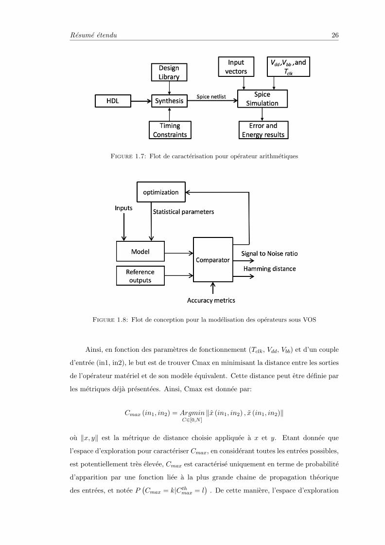
1.7 Flot de caracterisation pour operateur arithmetiques . . . . . . . . . . . . 26
1.8 Flot de conception pour la modelisation des operateurs sous VOS . . . . . 26
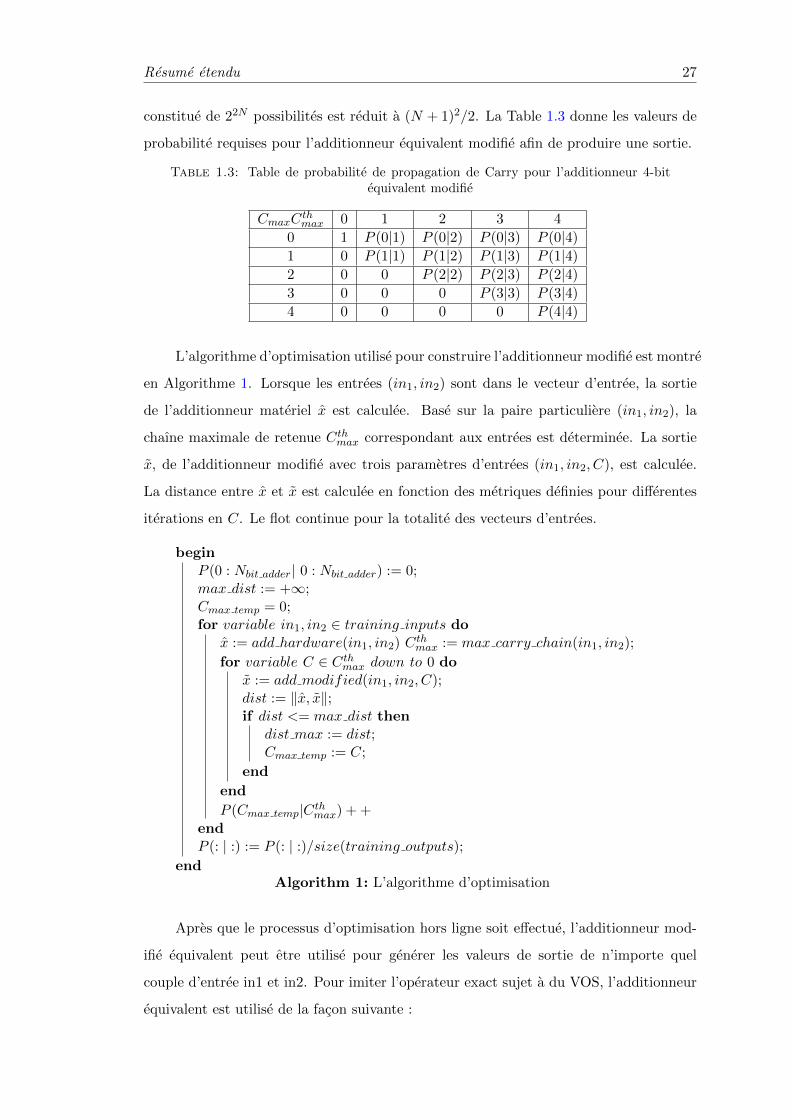
1.9 Erreur d’estimation du modele pour differents additionneurs et metriquesde distance . . . . . . . . . . . . . . . . . . . . . . . . . . . . . . . . . . . 29
1.10 Schema de l’organisation d’un ρ− V EX cluster . . . . . . . . . . . . . . . 30
1.11 Flot de caracterisation d’une unite d’execution d’un cluster ρ− V EX . . 31
1.12 Energie consommee en fonction du BER pour une UAL effectuant uneaddition . . . . . . . . . . . . . . . . . . . . . . . . . . . . . . . . . . . . . 32
1.13 Gestion de la tension d’une UAL pour atteindre une haute efficaciteenergetique . . . . . . . . . . . . . . . . . . . . . . . . . . . . . . . . . . . 33
1.14 BER d’une UAL pour le calcul approximatif . . . . . . . . . . . . . . . . . 33
1.15 Estimation d’energie pour differents benchmarks et pour differents Vdd,Vbb = 0V, et Tclk = 0.9ns . . . . . . . . . . . . . . . . . . . . . . . . . . . 36
1.16 Estimation d’energie d’une unite d’execution pour differents benchmarkspour differents Vdd, Vbb = 2V, et Tclk = 0.9ns . . . . . . . . . . . . . . . . 37
1.17 Estimation d’energie d’une unite d’execution pour differents benchmarkspour differents Vdd, Vbb = 0V, et Tclk = 0.45ns . . . . . . . . . . . . . . . 37
1.18 Estimation d’energie d’une unite d’execution pour differents benchmarkspour differents Vdd, Vbb = 2V, et Tclk = 0.45ns . . . . . . . . . . . . . . . 38
1.19 Perspective generale de la these . . . . . . . . . . . . . . . . . . . . . . . . 41
2.1 Task distribution without and with DVFS scheme . . . . . . . . . . . . . 47
2.2 Block diagram of Dynamic Voltage Scaling (DVS) . . . . . . . . . . . . . 48
2.3 Block diagram of Adaptive Voltage Scaling (AVS) . . . . . . . . . . . . . 48
2.4 Energy and delay in different Vdd regimes [22] . . . . . . . . . . . . . . . 49
2.5 Bluk CMOS vs FDSOI [31] . . . . . . . . . . . . . . . . . . . . . . . . . . 52
3.1 Timing errors due to the variability effects . . . . . . . . . . . . . . . . . . 58
3.2 Taxonomy of timing error tolerance at different abstractions [33] . . . . . 58
5

List of figures 6
3.3 Critical Path Emulation based error detection [1] . . . . . . . . . . . . . . 61
3.4 Schematic of Canary Flip Flop based error prediction . . . . . . . . . . . 62
3.5 Razor I based error detection [35] . . . . . . . . . . . . . . . . . . . . . . . 63
3.6 Schematic of Razor II latch and its internal components [37] . . . . . . . . 65
3.7 Razor II timing plot [37] . . . . . . . . . . . . . . . . . . . . . . . . . . . . 65
3.8 Schematic of Bubble Razor method [38] . . . . . . . . . . . . . . . . . . . 67
3.9 Bubble Razor timing plot [38] . . . . . . . . . . . . . . . . . . . . . . . . . 68
3.10 Schematic of latch based GRAAL method [39] . . . . . . . . . . . . . . . 69
3.11 GRAAL error correction using shadow flip-flop [39] . . . . . . . . . . . . . 69
3.12 TMR based on FEHM [42] . . . . . . . . . . . . . . . . . . . . . . . . . . 70
3.13 Schematic of FEHM block [42] . . . . . . . . . . . . . . . . . . . . . . . . 71
3.14 DDMR based FIR (Finite Impulse Response) filter [46] . . . . . . . . . . . 72
4.1 Schematic of FIR filter overclocking in Virtex FPGA . . . . . . . . . . . . 79
4.2 Timing errors (percentage of failing critical paths and output bit errorrate) vs. Overclocking in FPGA configured with an 8-bit 8-tap FIR filter 79
4.3 Principle of the double-sampling method to tackle timing errors . . . . . . 81
4.4 Principle of online slack measurement for overclocking . . . . . . . . . . . 82
4.5 Principle of the dynamic speculation window based double-sampling method.Solid lines represent data and control between modules, dashed lines rep-resent main clock, dash-dot-dash lines represent shadow clock, and dottedlines represent feedback control . . . . . . . . . . . . . . . . . . . . . . . . 83
4.6 Timing diagram of the proposed method. (a): Slack measurement phase,(b): Maximum overclocking margin, and (c): Impact of temperature atmaximum overclocking frequency . . . . . . . . . . . . . . . . . . . . . . . 84
(a) Scenario 1 . . . . . . . . . . . . . . . . . . . . . . . . . . . . . . . . . 84
(b) Scenario 2 . . . . . . . . . . . . . . . . . . . . . . . . . . . . . . . . . 84
(c) Scenario 3 . . . . . . . . . . . . . . . . . . . . . . . . . . . . . . . . . 84
4.7 Experimental setup of Adaptive overclocking based on Dynamic Speculation 88
4.8 Overclocking versus temperature for different benchmarks . . . . . . . . . 91
4.9 Comparison of Razor-based feedback look and the proposed dynamicspeculation window. Curve in blue diamond represents the FPGA’s coretemperature. Curve in red square represents the frequency scaling by theproposed method. Green triangle curve represents the frequency scalingby the Razor-based method . . . . . . . . . . . . . . . . . . . . . . . . . . 92
5.1 Accurate approximate configuration of [49] . . . . . . . . . . . . . . . . . 99
5.2 Approximate operator based on VOS . . . . . . . . . . . . . . . . . . . . 99
5.3 Proposed design flow for arithmetic operator characterization . . . . . . . 101
5.4 Carry Chain of Brent-Kung Adder [66] . . . . . . . . . . . . . . . . . . . . 103
5.5 Distribution of BER in output bits of 8-bit RCA under voltage scaling . . 103
5.6 Distribution of BER in output bits of 8-bit BKA under voltage scaling . . 104
5.7 Functional equivalence for hardware adder . . . . . . . . . . . . . . . . . . 104
5.8 Design flow of modelling of VOS operators . . . . . . . . . . . . . . . . . . 106
5.9 Estimation error of the model for different adders and distance metrics . . 108
5.10 Bit-Error Rate vs. Energy/Operation for 8-bit RCA . . . . . . . . . . . . 111
5.11 Bit-Error Rate vs. Energy/Operation for 8-bit BKA . . . . . . . . . . . . 112
5.12 Bit-Error Rate vs. Energy/Operation for 16-bit RCA . . . . . . . . . . . . 112

List of figures 7
5.13 Bit-Error Rate vs. Energy/Operation for 16-bit BKA . . . . . . . . . . . 113
6.1 Schematic of ρ− V EX Organization . . . . . . . . . . . . . . . . . . . . . 118
6.2 Instruction layout of ρ− V EX cluster . . . . . . . . . . . . . . . . . . . . 119
6.3 Toolchain for ρ− V EX processor . . . . . . . . . . . . . . . . . . . . . . 120
6.4 Block diagram of ALU and MUL units in ρ− V EX cluster . . . . . . . . 125
6.5 Schematic of characterization of execution unit of ρ− V EX cluster . . . 125
6.6 Energy versus Bit Error Rate (BER) plot of ALU executing ADD operation127
6.7 Voltage scaling of ALU to achieve high energy efficiency . . . . . . . . . . 127
6.8 Bit Error Rate (BER) plot of ALU and scope for approximate computing 128
6.9 Energy versus Bit Error Rate (BER) plot of ALU executing SUB operation128
6.10 Energy versus Bit Error Rate (BER) plot of ALU executing DIV operation129
6.11 Energy versus Bit Error Rate (BER) plot of ALU executing AND operation130
6.12 Energy versus Bit Error Rate (BER) plot of ALU executing OR operation 131
6.13 Energy versus Bit Error Rate (BER) plot of ALU executing XOR operation132
6.14 ρ−V EX cluster blocks (highlighted) characterized of for energy estimation132
6.15 Flow graph of validation method . . . . . . . . . . . . . . . . . . . . . . . 136
6.16 Energy estimation of execution unit for Benchmarks with different Vdd,and no back-biasing at Tclk = 0.9ns . . . . . . . . . . . . . . . . . . . . . . 138
6.17 Energy estimation of execution unit for Benchmarks with different Vdd,with back-biasing Vbb = 2V, and Tclk = 0.9ns . . . . . . . . . . . . . . . . 139
6.18 Energy estimation of execution unit for Benchmarks with different Vdd,and no back-biasing at Tclk = 0.45ns . . . . . . . . . . . . . . . . . . . . . 140
6.19 Energy estimation of execution unit for Benchmarks with different Vdd,with back-biasing Vbb = 2V, and Tclk = 0.45ns . . . . . . . . . . . . . . . 140
7.1 Overall perspective of the thesis . . . . . . . . . . . . . . . . . . . . . . . . 146
A.1 Signed multiplier (Radix-4 modified Booth, Wallace Tree, and BKA) . . . 150
A.2 Unsigned multiplier (Simple PPG, Array, and RCA) . . . . . . . . . . . . 150
A.3 Distribution of BER in output bits of 16-bit Signed Multiplier . . . . . . . 151
A.4 Distribution of BER in output bits of 16-bit Unsigned Multiplier . . . . . 151

List of Tables
1.1 Fmax estimee et Fmax augmentee sans faute pour des architectures a 28◦C 21
1.2 Impact de la temperature sur l’augmentation de la frequence d’architecturesa 50◦C . . . . . . . . . . . . . . . . . . . . . . . . . . . . . . . . . . . . . . 21
1.3 Table de probabilite de propagation de Carry pour l’additionneur 4-bitequivalent modifie . . . . . . . . . . . . . . . . . . . . . . . . . . . . . . . 27
1.4 Details des programmes de test . . . . . . . . . . . . . . . . . . . . . . . . 36
4.1 Synthesis results of different benchmark designs . . . . . . . . . . . . . . . 90
4.2 Estimated Fmax and safe overclocking Fmax of benchmark designs at 28◦C 90
4.3 Impact of temperature while overclocking in benchmark designs at 50◦C . 91
5.1 Carry propagation probability table of modified 4-bit adder . . . . . . . . 106
5.2 Synthesis Results of 8 and 16 bit RCA and BKA . . . . . . . . . . . . . . 109
5.3 Operating triads used in Spice simulation . . . . . . . . . . . . . . . . . . 109
5.4 Energy Efficiency in 8-bit and 16-bit Ripple Carry and Brent-Kung Adders110
5.5 BER in 8-bit and 16-bit Ripple Carry and Brent-Kung Adders . . . . . . 111
6.1 Energy consumption of different VLIW instructions . . . . . . . . . . . . . 134
6.2 Energy consumption of different VLIW instructions with body bias . . . . 135
6.3 Validation of proposed energy estimation method . . . . . . . . . . . . . . 137
6.4 Benchmark Programs . . . . . . . . . . . . . . . . . . . . . . . . . . . . . 138
9


Chapter 1
Resume etendu
1.1 Introduction
L’efficacite energetique et la gestion des erreurs sont les deux challenges majeurs dans
la tendance grandissante de l’internet des objets. Une plethore de techniques, appelees
ultra faible consommation, ont ete explorees par le passe afin d’ameliorer l’efficacite
energetique des systemes numeriques. Ces techniques peuvent generalement se classer
au niveau technologique, au niveau architecture, ou au niveau conception. Au niveau
technologique, differentes technologies CMOS et SOI, par exemple le FDSOI de STMicro-
electronics ou le FinFET, beneficient de maniere inherente d’un faible courant de fuite
et de composants a faible consommation pour la conception numerique. De maniere
similaire, de nombreuses solutions architecturales a faible consommation sont utilisees
pour augmenter le gain energetique et le debit des architectures numeriques, comme
par exemple le pipeline, l’entrelacement, ou encore les architectures asynchrones. En-
fin, au niveau conception, des techniques telles que la desactivation de l’horloge ou de
l’alimentation, et l’adaptation de la frequence et de la tension, permettent egalement de
reduire la consommation energetique.
Au fil des ans, la gestion de la tension d’alimentation a ete utilisee comme tech-
nique principale pour augmenter l’efficacite energetique des systemes numeriques. En
effet, diminuer la tension d’alimentation permet de reduire de maniere quadratique la
11

Resume etendu 12
consommation energetique du systeme selon l’equation suivante :
Etotal = V 2dd.Cload (1.1)
Dans la litterature, des variantes de la technique de gestion de tension ont ete proposees
pour ameliorer l’efficacite energetique des systemes numeriques [1], [2]. L’ajustement
dynamique de la frequence et de la tension est devenu la principale technique pour
reduire l’energie en diminuant les performances d’une marge acceptable. D’un autre cote,
la diminution de la finesse de gravure des circuits integres augmente les risques dus aux
effets de variabilite. Les effets de variabilite causent des differences de fonctionnement
dans les circuits lies aux variations de fabrication, d’alimentation et de temperature
des circuits (Process, Voltage and Temperature – PVT). Les effets de la diminution
de tension et de frequence couples aux problemes de variabilite rendent les systemes
pipelines plus vulnerables aux erreurs temporelles [3]. Des mecanismes sophistiques
de detection et de correction des erreurs sont requis pour gerer ces erreurs. Dans la
litterature, de nombreuses methodes sont proposees, comme celles basees sur la methode
du double echantillonnage [4].
Les principales limitations des methodes actuelles de double echantillonnage sont :
une fenetre de speculation fixe (dephasage entre les deux horloges), le cout en ressources
du aux besoins de buffers et de detecteur de transition, et enfin la complexite des
methodes, comme par exemple la generation et la propagation des bulles (technique
Bubble Razor). De meme pour les techniques d’emprunt de temps (time borrow-
ing) qui necessitent des flots d’outil de conception specifiques afin de resynchroniser
l’architecture. Les methodes de redondance materiel, telles que la duplication et la trip-
lication sont tres consommatrices de ressources, ce qui les rend plus interessantes pour
des architectures reconfigurables, du type FPGA, disposant de nombreuses ressources
inutilisees. Les applications basees sur le calcul probabiliste peuvent tolerer une marge
d’erreur sans compromettre la qualite de la sortie generee. Ainsi, il y a un besoin
d’unifier les approches afin de gerer les erreurs en fonction des applications et du be-
soin utilisateur. La methode requise doit etre capable de detecter et de corriger des
erreurs tout en permettant a l’utilisateur de choisir un compromis entre la precision des
calculs et l’efficacite energetique. Finalement, il y a un besoin d’associer les differentes
techniques de tres faible consommation telles que l’ajustement dynamique de la tension
et l’alimentation proche du seuil de basculement. Dans cette these, nous proposons
Resume etendu 13
un framework pour estimer l’energie et gerer les erreurs dans le contexte d’architecture
alimentee proche du seuil pour les applications resistantes aux erreurs.
1.2 Contributions
Les contributions de la these sont les suivantes.
1. Une speculation temporelle dynamique basee sur l’ajustement dynamique de la
frequence et la correction d’erreur pour un chemin de donnees pipeline est proposee.
Cette methode permet d’identifier dynamiquement la possibilite d’augmenter la
frequence du systeme, et permet egalement de repondre aux effets de variabilite en
la diminuant. Cela est effectue sur la base d’une mesure de la marge temporelle en-
tre les signaux de sortie des registres et l’horloge via le principe du registre dephase
(shadow register). S’il y a des erreurs temporelles dues a des effets de variabilite,
un mecanisme de correction embarque permet de gerer les erreurs sans re-executer
les instructions. Contrairement aux methodes de type Razor, des buffers addition-
nels ne sont pas requis pour les chemins logiques les plus court. L’efficacite de
cette methode est mise en œuvre sur le FPGA Virtex 7 de Xilinx. Les resultats
montrent qu’une augmentation de la frequence de 71% peut etre atteinte avec un
surcout materiel limite.
2. La precision et l’efficacite energetique de differents additionneurs et multiplieurs
sont caracterisees pour de nombreuses configurations de fonctionnement. Un
Framework est propose pour modeliser statistiquement le comportement des operateurs
sujets a un ajustement agressif de la tension. Les modeles generes peuvent etre
utilises dans le calcul approximatif au niveau algorithmique. Les resultats de sim-
ulation montrent une reduction energetique pouvant atteindre 89% en contrepartie
d’un taux d’erreur binaire de 20%.
3. Un Framework est propose pour estimer la consommation energetique au niveau
fonctionnel d’une architecture de processeur a mot d’instruction tres long (Very
Long Instruction Word – VLIW). Un flot d’outil a ete developpe pour analyser
des programmes de reference (benchmarks) et rapidement estimer des metriques
d’energie et d’erreur pour differents parametres de fonctionnement. Une rapide es-
timation est possible en utilisant un compilateur C et VEX. Cette estimation peut
Resume etendu 14
etre utilisee pour configurer dynamiquement les parametres de fonctionnement
afin d’atteindre un meilleur compromis entre l’energie et la precision de calcul.
Une validation de notre Framework est effectuee sur le processeur VLIW p-Vex.
L’unite d’execution du processeur est caracterisee pour differentes configurations et
la consommation d’energie au niveau fonctionnelle est estimee avec le Framework
propose.
1.3 Gestion des erreurs temporelles
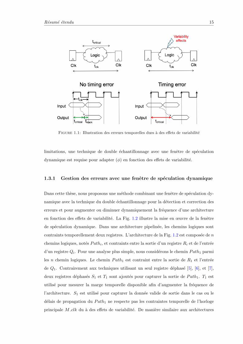
Comme illustre en Fig. 1.1, les architectures numeriques sont contraintes temporelle-
ment avec une marge positive pour la synchronisation en visant un compromis entre
performance et effet des variabilites. Une architecture subissant des effets de variabilite
peut voir une augmentation dans les delais de propagation de ses portes resultant en er-
reurs temporelles (le signal atteint sa valeur finale apres le declenchement du registre de
sortie). De telles erreurs peuvent etre corrigees mais au prix d’un surcout materiel [4].
La methode Razor est une technique bien connue pour la detection et correction des
erreurs temporelles dans les systemes numeriques, elle s’inspire de la methode du dou-
ble echantillonnage [4]. Dans les architectures utilisant le double echantillonnage, un
registre supplementaire, appele registre dephase (shadow register) est utilise en plus du
registre de sortie afin de capturer la valeur de sortie a des instants differents. Le registre
dephase utilise une horloge dephasee (shadow clock), par rapport a l’horloge principale.
L’ecart temporel entre le front montant de l’horloge principale et de l’horloge dephasee
est appele fenetre de speculation (φ). La fenetre de speculation est utilisee pour com-
parer la valeur de sortie du registre principal et du registre dephasee afin de determiner
la validite de la sortie.
Il y a un compromis a effectuer entre la taille de la fenetre de speculation et le
taux de couverture de faute. Pour une fenetre de speculation large, plus d’erreurs peu-
vent etre detectees et corrigees, mais cela necessite plus d’insertion de buffer pour les
chemin logiques ayant un delais de propagation plus rapide que (φ) afin d’eviter des
fausses detections. L’effet est inverse pour une fenetre de speculation courte. Les ar-
chitectures avec une fenetre de speculation fixe optimisee pour certaines conditions de
fonctionnement peuvent souffrir d’une augmentation du taux d’erreur sous certaines
variabilites, comme par exemple les variations de temperature. Afin de repondre a ces
Resume etendu 15
Figure 1.1: Illustration des erreurs temporelles dues a des effets de variabilite
limitations, une technique de double echantillonnage avec une fenetre de speculation
dynamique est requise pour adapter (φ) en fonction des effets de variabilite.
1.3.1 Gestion des erreurs avec une fenetre de speculation dynamique
Dans cette these, nous proposons une methode combinant une fenetre de speculation dy-
namique avec la technique du double echantillonnage pour la detection et correction des
erreurs et pour augmenter ou diminuer dynamiquement la frequence d’une architecture
en fonction des effets de variabilite. La Fig. 1.2 illustre la mise en œuvre de la fenetre
de speculation dynamique. Dans une architecture pipelinee, les chemins logiques sont
contraints temporellement deux registres. L’architecture de la Fig. 1.2 est composee de n
chemins logiques, notes Pathi, et contraints entre la sortie d’un registre Ri et de l’entree
d’un registre Qi. Pour une analyse plus simple, nous considerons le chemin Path1 parmi
les n chemin logiques. Le chemin Path1 est contraint entre la sortie de R1 et l’entree
de Q1. Contrairement aux techniques utilisant un seul registre dephase [5], [6], et [7],
deux registres dephases S1 et T1 sont ajoutes pour capturer la sortie de Path1. T1 est
utilise pour mesurer la marge temporelle disponible afin d’augmenter la frequence de
l’architecture. S1 est utilise pour capturer la donnee valide de sortie dans le cas ou le
delais de propagation du Path1 ne respecte pas les contraintes temporelle de l’horloge
principale M clk du a des effets de variabilite. De maniere similaire aux architectures
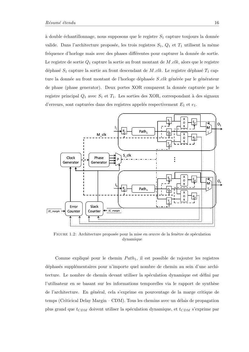
Resume etendu 16
a double echantillonnage, nous supposons que le registre S1 capture toujours la donnee
valide. Dans l’architecture proposee, les trois registres S1, Q1 et T1 utilisent la meme
frequence d’horloge mais avec des phases differentes pour capturer la donnee de sortie.
Le registre de sortie Q1 capture la sortie au front montant de M clk, alors que le registre
dephase S1 capture la sortie au front descendant de M clk. Le registre dephase T1 cap-
ture la donnee au front montant de l’horloge dephasee S clk generee par le generateur
de phase (phase generator). Deux portes XOR comparent la donnee capturee par le
registre principal Q1 avec S1 et T1. Les sorties des XOR, correspondant a des signaux
d’erreurs, sont capturees dans des registres appeles respectivement E1 et e1.
Figure 1.2: Architecture proposee pour la mise en œuvre de la fenetre de speculationdynamique
Comme explique pour le chemin Path1, il est possible de rajouter les registres
dephases supplementaires pour n’importe quel nombre de chemin au sein d’une archi-
tecture. Le nombre de chemin devant utiliser la speculation dynamique est defini par
l’utilisateur en se basant sur les informations temporelles via le rapport de synthese
de l’architecture. En general, cela s’exprime en pourcentage de la marge critique de
temps (Criticical Delay Margin – CDM). Tous les chemins avec un delais de propagation
plus grand que tCDM doivent utiliser la speculation dynamique, et tCDM s’exprime par

Resume etendu 17
l’equation suivante
tCDM = tcritical − (tcritical.CDM) (1.2)
dans laquelle tcritical est la valeur du chemin critique. Dans la Fig. 1.2, CDM = 100%.
Cela signifie que les n chemins de l’architecture disposent de registre pour la speculation
dynamique. Pour des applications tels que les filtres a reponse impulsionnelle finie
(Finite Impulse Response – FIR), dans lesquelles presque tous les chemins ont le meme
delai de propagation, un CDM de 100% est requis. Au contraire, pour des applications
avec des chemins ayant des delais de propagation plus distribues, le CDM peut varier
de 10 a 20%.
1.3.2 Boucle de retour pour augmentation ou diminution de la frequence
La Fig. 1.2 montre la boucle de retour de la methode proposee. Les signaux d’erreur
Ei et ei des chemins monitores sont connectes respectivement au compteur d’erreur
(Error Counter) et au compteur de marge (Slack Counter). Pour differentes fenetres
de speculation φi, Error Counter et Slack Counter comptent les variations dans les
chemins concernes.
• Le Slack Counter determine le nombre d’erreur liee a l’augmentation de la frequence
ou a la diminution de la tension d’alimentation.
• Le Error Counter determine le nombre d’erreur temporelle liee a des effets de
variabilite.
Pour une architecture, utilisant une horloge configuree au maximum de la frequence
possible et sans effet liee a la variabilite, Error Counter et Slack Counter sont a 0.
Cela indique qu’il n’y a pas d’erreur dans l’architecture. Afin d’augmenter les perfor-
mances, l’architecture peut subir une augmentation de la frequence. Le generateur de
phase dans la boucle de retour est utilise pour generer differentes phases pour l’horloge
S clk. Cette horloge sert a determiner s’il y a une marge sure afin d’augmenter la
frequence (sans generer d’erreur) en mesurant la marge temporelle disponible. Dans
la methode proposee, un registre dedie est utilise pour mesurer la marge disponible.
Lorsque la difference de phase φ entre M clk et S clk augmente, les chemins critiques
de l’architecture ont tendance a devenir fautifs indiquant la limite pour augmenter la
Resume etendu 18
frequence de maniere sure. Le registre determinant la marge temporelle Ti detecte cette
erreur temporelle et augmente le Slack Counter du nombre de chemin defaillant. Dans
ce cas, Error Counter reste a zero tant que le pipeline ne subit pas d’erreur. En fonction
de la valeur du Slack Counter, une augmentation de la frequence ou une diminution de
la tension est geree par la boucle de retour.
Certaines applications tolerantes aux erreurs peuvent tolerer un certain nombre
d’erreurs. Dans la boucle de retour, SC margin est une marge d’erreur tolerable definie
par l’utilisateur. Pour les applications pouvant tolerer les erreurs temporelles, SC margin
peut etre configuree pour permettre un reglage de frequence ou de tension afin d’augmenter
respectivement les performances ou l’efficacite energetique, meme en presence d’erreurs.
Dans le cas ou des effets de variabilite se manifestent, des chemins logiques vont subir
des erreurs, ce qui va incrementer la valeur du Error Counter en fonction du nombre de
chemin fautif. Cela declenche le mecanisme de correction d’erreur consistant a fournir
a l’etage suivant du pipeline la valeur stockee dans le registre dephase Si au lieu de
celle stockee dans le registre principal. En fonction de la valeur du Error Counter, la
boucle de retour peut decider de reduire la frequence d’horloge ou d’augmenter la tension
d’alimentation afin de reduire les erreurs temporelles. Comme mentionne precedemment,
Error Counter permet de configurer une marge d’erreur tolerable pour les applications
resistantes aux erreurs. Tant que cette marge n’est pas depassee, l’architecture ne subit
pas de reajustement sur la frequence ou la tension d’alimentation. De meme, EC margin
configure la limite pour les erreurs temporelles dues a des effets de variabilite qui peuvent
etre tolerees sans compromettre la performance ou l’efficacite energetique.
SC margin et EC margin sont definis comme pourcentage du CDM. Pour des ap-
plications necessitant une grande precision, SC margin et EC margin sont mis a 0%.
Cela force la boucle de retour a augmenter la frequence de maniere sure (sans generer
d’erreur) et ne tolere aucune erreur temporelle du a des problemes de variabilite. Les
marges tolerables d’erreur pour l’Error Counter et le Slack Counter sont determinees
a partir des rapports de synthese et de placement de l’architecture.
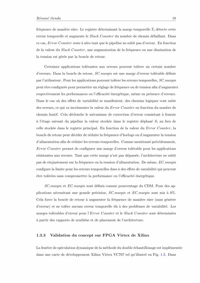
1.3.3 Validation du concept sur FPGA Virtex de Xilinx
La fenetre de speculation dynamique de la methode du double echantillonage est implementee
dans une carte de developpement Xilinx Virtex VC707 tel qu’illustre en Fig. 1.3. Dans
Resume etendu 19
cette experimentation, nous avons demontre la gestion dynamique de la frequence dans
un FPGA Virtex 7 via la methode de speculation dynamique. Cette methode peut
etre etendue a l’adaptation de la tension sur les plate-formes qui sont compatible avec
la gestion de cette derniere. La chaıne d’outil Vivado est utilisee pour synthetiser et
implementer les architectures de demonstration dans le FPGA. Un vecteur de test (test-
bench) aleatoire est cree pour chaque architecture via un generateur de vecteur LFSR de
80 bits. L’oscillateur LVDS programmable par IIC est utilise pour generer la frequence
d’horloge pour le generateur de vecteur de test et l’architecture de demonstration.
Comme illustre en Fig. 1.3, les signaux de controles du compteur d’erreurs (Error Counter)
et du compteur de marge (Slack Counter) determinent la frequence de sortie de l’oscillateur
LVDS. Les differentes phases des horloges generees sont obtenues via le module de gestion
d’horloge integre au FPGA (Mixed-Mode Clock Manager : MMCM ). La temperature
du coeur est mesuree via le moniteur XADC, et la temperature est reglee en changeant
la vitesse de rotation du ventilateur.
Figure 1.3: Configuration de l’experimentation de l’overclocking base sur laspeculation dynamique
Pour une gestion dynamique de la frequence sans erreur, la marge Slack Counter
est configuree a zero. A la temperature ambiante de 28◦C, lorsque Error Counter et
Slack Counter sont egaux a zero, la fenetre de speculation φ est augmentee a chaque
cycle d’horloge de 0◦ a 180◦ par intervalle de 25◦ jusqu’a ce que le Slack Counter
enregistre une erreur. Au dela de 180◦, et jusqu’a 360◦, la fenetre de speculation se
repete du a la nature periodique de l’horloge. Lorsque le Slack Counter enregistre une
Resume etendu 20
erreur, cela indique que la marge maximale a ete definie. Le systeme est mis en pause et
est overlocke de maniere sure en respectant la marge disponible. Lorsque la fenetre de
speculation φ est balayee, le pipeline fonctionne normalement des lors que les sorties du
registre Qi et du registre dephase Si capturent la donnee valide. Concernant la correction
des erreurs dues aux effets de variabilites, si Erreur Counter detecte que plus de 2%
des chemins monitores ne respectent pas les contraintes de temps, le systeme est mis
en pause et la frequence du systeme est diminuee par multiple d’un pas de frequence
δ afin de reduire ces erreurs (dans notre plateforme de test, le pas de frequence est
δ = 5MHz). Etant donnee que corriger plus d’erreurs reduit la bande passante de
l’architecture, diminuer la frequence est une mesure necessaire. Le multiplexeur Mi, tel
qu’illustre dans la Fig. 1.2, corrige l’erreur en connectant la sortie du registre dephase
Si au prochain etage du pipeline. Des que la temperature diminue, la frequence de
fonctionnement de l’architecture est de nouveau augmentee en fonction de la marge
mesuree tel que decrit precedemment.
Pour mettre en avant l’adaptation dynamique de la frequence et la capacite a
detecter et corriger les erreurs de la methode proposee, nous avons implemente un en-
semble d’architectures de test avec la methode Razor [5] et la methode proposee base
sur la fenetre de speculation dynamique. Les architectures de test utilisees dans ces
experimentations sont des elements de chemin de donnees tels que les filtres FIR, et de
nombreuses version d’architectures 32bits d’additionneurs et de multiplieurs. Apres
implementation, les rapports generes permettent de definir les chemins critiques de
chaque architecture.
Pour une architecture a temperature ambiante d’environ 25◦C, la fenetre de speculation
φ est augmentee a chaque cycle d’horloge. Si le Slack Counter est egale a zero a la plus
large fenetre de speculation, alors la frequence d’horloge peut etre augmentee de 40%
etant donnee qu’a 180◦, φ correspond a la moitie de la periode d’horloge. Cela im-
plique que tous les chemins critiques de l’architectures ont une marge positive egale
a la moitie de la periode d’horloge. L’augmentation de la frequence est effectuee en
stoppant l’architecture et en augmentant la frequence d’horloge a partir de l’oscillateur
LVDS. Apres ce changement de frequence, l’etape de balayage de phase recommence a
0◦ jusqu’a ce que Slack Counter enregistre une erreur. Alors que l’architecture fonc-
tionne a une frequence augmentee Fmax a 28◦C, la temperature de la puce est aug-
mentee en faisant varier la frequence de rotation du ventilateur de refroidissement. Due

Resume etendu 21
Table 1.1: Fmax estimee et Fmax augmentee sans faute pour des architectures a 28◦C
ArchitectureFmax
Fmax Marge
estimee (MHz)sans faute d’augmentation
a 28◦C de Fmax
(MHz) a 28◦C
8-tap 8-bit FIR 167 260 55%
Multiplieur non-signe 32-bit 76 130 71%
Multiplieur signe 32-bit Wallace Tree 80 135 69%
Additionneur 32-bit Kogge-Stone 130 215 64%
Additionneur 32-bit Brent-Kung 135 216 60%
Table 1.2: Impact de la temperature sur l’augmentation de la frequenced’architectures a 50◦C
Architectures
% des chemins Fmax Margedefaillant sans faute d’augmentation
a 50◦C pour a 50◦C sans fauteFmax a 28◦C ( MHz) a 50◦C
Filtre 8-tap 8-bit FIR 12 180 8%
Miltiplieur non-signe 32-bit 22 85 12%
Miltiplieur signe 32-bit Wallace Tree 26 85 7%
Additionneur 32-bit Kogge-Stone 13 180 38%
Additionneur 32-bit Brent-Kung 21 180 33%
a l’augmentation de la temperature, les chemins critiques de l’architecture commencent
a defaillir. Lorsque Error Counter detecte plus que 2% des chemins monitores sont
fautifs, l’architecture est mis en pause et la frequence d’horloge est reduite par multiple
de 5MHZ jusqu’a ce que la marge Error Counter est sous les 2%.
La Table 1.1 montre la Fmax estimee pour chaque architecture de test ainsi que la
Fmax maximale pouvant etre atteinte sans erreur par la methode de detection d’erreur
proposee a une temperature ambiante de 28◦C. Par exemple, pour l’architecture du
filtre FIR, Vivado a estime Fmax a 167MHz. Cependant, cette architecture peut avoir
sa frequence augmentee, a temperature ambiante, de plus de 55% jusqu’a 260MHz et sans
erreur, et jusqu’a 71% pour les autres architectures de test. A la frequence maximale
sans erreur, la temperature est augmentee de 28◦C a 50◦C, a laquelle Error Counter
detecte que 12% des chemins de donnees sont defaillants. Etant donnee que le nombre
de chemins fautifs est superieur a la marge configuree a 2%, la frequence d’horloge
de l’oscillateur LVDS est diminuee jusqu’a 180MHz. Cette diminution de la frequence
permet de maintenir le nombre de chemin fautif a moins de 2%. La Table 1.2 liste
l’impact de la temperature et la marge d’augmentation de la frequence sans erreur pour

Resume etendu 22
une temperature de 50◦C pour toutes les architectures de test. Le pourcentage de chemin
monitore qui sont defaillant a 50◦C montrent l’impact de la temperature lorsque l’on
overclock l’architecture.
Lorsque la temperature redescend a 28◦C, la marge temporelle disponible est mesuree
en temps reel et la frequence d’horloge est augmentee afin d’atteindre des performances
maximales. Ces resultats demontrent la gestion dynamique de la frequence d’horloge,
ainsi que la capacite de detection et de correction des erreurs de la methode proposee
avec un surcout materiel limite.
Figure 1.4: Comparaison entre une boucle de retour utilisant la methode Razor et latechnique proposee
La Fig. 1.4 montre la comparaison entre la fenetre de speculation dynamique et
la methode Razor pour un filtre FIR 8-bit 8-tap au sein d’un FPGA Virtex 7. La
temperature du circuit est modifiee en faisant varier la vitesse de rotation du ventilateur.
Comme montre en Fig. 1.4, la temperature du circuit est augmentee a partir de la
temperature ambiante de 28◦C jusqu’a 50◦C, puis diminuee a nouveau jusqu’a 28◦C.
Lorsque la temperature commence a augmenter, les chemins critiques de l’architecture
commencent a defaillir, ce qui diminue la frequence d’horloge via la methode proposee et
celle utilisant Razor afin de rester sous la limite des 2% de chemin fautif. Initiallement,
a temperature ambiante, l’architecture fonctionne a 260MHz. A la temperature de 50◦C
la frequence est diminuee a 180MHz. Lorsque la temperature retourne a celle d’origine,
la methode proposee est capable de mesurer la marge disponible et d’augmenter la
frequence d’horloge. Au contraire, la methode Razor ne modifie pas la frequence. En

Resume etendu 23
effet, cette methode n’integre pas de mesure de marge temporelle disponible. Cela donne
un avantage certain a la methode proposee.
1.4 Ajustement agressif de l’alimentation pour les appli-
cations resistantes aux erreurs
Comme mentionne dans la section precedente, des applications basees sur des algo-
rithmes statistiques et probabilistes, par exemple pour le calcul video, la reconnaissance
d’image, l’exploitation large echelle de donnees et de texte, ont une capacite inherente a
tolerer les incertitudes liees au materiel. De telles applications peuvent fonctionner avec
des erreurs, evitant ainsi le besoin de materiel supplementaire pour detecter et corriger
les erreurs. Ainsi, les applications resilientes aux erreurs sont une opportunite pour la
conception d’architecture approximative pour satisfaire les besoins de calcul avec une
meilleure efficacite energetique. Dans les applications resilientes aux erreurs, le calcul
approximatif peut etre introduit a differents niveaux et a differentes granularites.
Dans ce travail, nous utilisons une diminution agressive de la tension d’alimentation
(voltage overscaling) dans les operateurs arithmetiques ce qui cause deliberement des
approximations au niveau du circuit. En reduisant la tension d’alimentation vers le
niveau du seuil des transistors, des erreurs dues a des delais de propagation peuvent
survenir. Le comportement des operateurs arithmetiques fonctionnant a la region proche,
ou sous le seuil, est different par rapport a une tension d’alimentation elevee (super
threshold region). Dans le cas d’un additionneur a propagation de retenu (Ripple Carry
Adder – RCA), lorsque la tension d’alimentation diminue, le comportement attendue
est une defaillance des chemins critiques, en commencant par le plus long jusqu’au plus
court, en fonction de la diminution de la tension d’alimentation. La Fig. 1.5 montre l’effet
de la diminution de tension pour un RCA 8 bits. Lorsque la tension d’alimentation est
diminuee de 1V a 0,8V, les bits de poids forts commencent a etre errones. Lorsque
la tension continue a diminuer, de 0,7V a 0,6V, le plus grand taux d’erreur binaire
(Bit Error Rate – BER) apparaıt sur les bits de poids moyens plutot que sur les bits
de poids forts. Pour une alimentation de 0,5V, presque tous les bits atteignent 50%
ou plus de BER. Ce comportement impose des limitations dans la modelisation des
operateurs arithmetiques dans la region proche/sous le seuil en utilisant des modeles
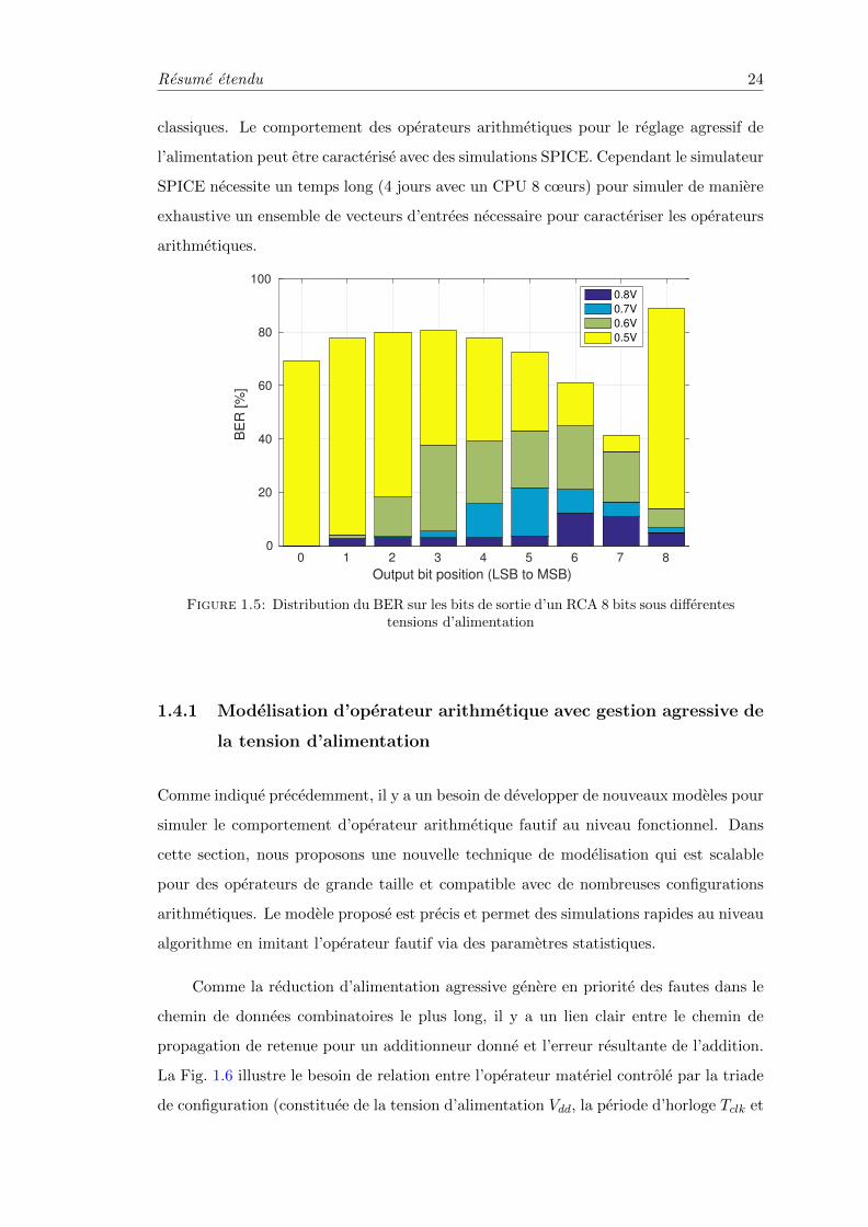
Resume etendu 24
classiques. Le comportement des operateurs arithmetiques pour le reglage agressif de
l’alimentation peut etre caracterise avec des simulations SPICE. Cependant le simulateur
SPICE necessite un temps long (4 jours avec un CPU 8 cœurs) pour simuler de maniere
exhaustive un ensemble de vecteurs d’entrees necessaire pour caracteriser les operateurs
arithmetiques.
0 1 2 3 4 5 6 7 8
Output bit position (LSB to MSB)
0
20
40
60
80
100
BE
R [
%]
0.8V
0.7V
0.6V
0.5V
Figure 1.5: Distribution du BER sur les bits de sortie d’un RCA 8 bits sous differentestensions d’alimentation
1.4.1 Modelisation d’operateur arithmetique avec gestion agressive de
la tension d’alimentation
Comme indique precedemment, il y a un besoin de developper de nouveaux modeles pour
simuler le comportement d’operateur arithmetique fautif au niveau fonctionnel. Dans
cette section, nous proposons une nouvelle technique de modelisation qui est scalable
pour des operateurs de grande taille et compatible avec de nombreuses configurations
arithmetiques. Le modele propose est precis et permet des simulations rapides au niveau
algorithme en imitant l’operateur fautif via des parametres statistiques.
Comme la reduction d’alimentation agressive genere en priorite des fautes dans le
chemin de donnees combinatoires le plus long, il y a un lien clair entre le chemin de
propagation de retenue pour un additionneur donne et l’erreur resultante de l’addition.
La Fig. 1.6 illustre le besoin de relation entre l’operateur materiel controle par la triade
de configuration (constituee de la tension d’alimentation Vdd, la periode d’horloge Tclk et

Resume etendu 25
la tension de polarisation inverse Vbb) et le modele statistique controle par des parametres
statistiques Pi. La connaissance des valeurs d’entrees fournie les informations necessaires
concernant la plus longue chaıne de propagation de retenu, ainsi les valeurs d’entrees
sont utilisees pour generer les parametres statistiques qui controlent le modele equivalent.
Ces parametres statistiques sont obtenus a travers un processus d’optimisation hors ligne
qui minimise les differences entre les sorties de l’operateur et de son modele statistique
equivalent, avec le respect de certaines metriques. Dans ce travail, nous avons utilise
trois metriques pour calibrer l’efficacite de notre modele statistique : l’erreur quadratique
moyenne (Mean Square Error – MSE), la distance de Hamming (Hamming distance) et
la distance de Hamming ponderee (Weighted Hamming distance).
Hardware
Operator
Tclk Vdd Vbb
in1
in2
xin1
in2
CtrlP1,P2,P3,P4
^ x~
Figure 1.6: Equivalence fonctionnelle de l’additionneur materiel
1.4.2 Validation du concept: modelisation d’additionneurs
Dans le reste de cette section, une validation du concept est effectuee en appliquant
une gestion agressive de l’alimentation (Voltage Overscaling – VOS) pour differentes
configurations d’additionneurs. Tous les additionneurs subissent le VOS et sont car-
acterises par le flot decrit par la Fig. 1.7. La Fig. 1.8 montre le flot de conception pour
modeliser les operateurs avec VOS. Comme illustre en Fig. 1.6, un modele rudimentaire
de l’operateur materiel est cree avec les vecteurs d’entrees et les parametres statistiques.
Pour un vecteur d’entree donne, les sorties du modele et de l’operateur materiel sont
comparees en se basant sur les metriques definies precedemment. Le comparateur il-
lustre en Fig. 1.8 genere le rapport signal sur bruit (Signal to Noise Ration – SNR) et la
distance de Hamming pour determiner la qualite du modele en fonction des metriques.
Le SNR et la distance de Hamming sont renvoyes dans un algorithme d’optimisation
afin de configurer plus finement le modele representant l’operateur sous VOS. Dans le
cas d’additionneurs, seulement un parametre Pi est utilise pour le modele statistique. Il
est defini par Cmax, la longueur de la plus grande chaıne de retenu a propager.
Resume etendu 26
Figure 1.7: Flot de caracterisation pour operateur arithmetiques
Figure 1.8: Flot de conception pour la modelisation des operateurs sous VOS
Ainsi, en fonction des parametres de fonctionnement (Tclk, Vdd, Vbb) et d’un couple
d’entree (in1, in2), le but est de trouver Cmax en minimisant la distance entre les sorties
de l’operateur materiel et de son modele equivalent. Cette distance peut etre definie par
les metriques deja presentees. Ainsi, Cmax est donnee par:
Cmax (in1, in2) = ArgminC∈[0,N ]
‖x (in1, in2) , x (in1, in2)‖
ou ‖x, y‖ est la metrique de distance choisie appliquee a x et y. Etant donnee que
l’espace d’exploration pour caracteriser Cmax, en considerant toutes les entrees possibles,
est potentiellement tres elevee, Cmax est caracterise uniquement en terme de probabilite
d’apparition par une fonction liee a la plus grande chaine de propagation theorique
des entrees, et notee P(Cmax = k|Cth
max = l)
. De cette maniere, l’espace d’exploration
Resume etendu 27
constitue de 22N possibilites est reduit a (N + 1)2/2. La Table 1.3 donne les valeurs de
probabilite requises pour l’additionneur equivalent modifie afin de produire une sortie.
Table 1.3: Table de probabilite de propagation de Carry pour l’additionneur 4-bitequivalent modifie
CmaxCthmax 0 1 2 3 4
0 1 P (0|1) P (0|2) P (0|3) P (0|4)
1 0 P (1|1) P (1|2) P (1|3) P (1|4)
2 0 0 P (2|2) P (2|3) P (2|4)
3 0 0 0 P (3|3) P (3|4)
4 0 0 0 0 P (4|4)
L’algorithme d’optimisation utilise pour construire l’additionneur modifie est montre
en Algorithme 1. Lorsque les entrees (in1, in2) sont dans le vecteur d’entree, la sortie
de l’additionneur materiel x est calculee. Base sur la paire particuliere (in1, in2), la
chaıne maximale de retenue Cthmax correspondant aux entrees est determinee. La sortie
x, de l’additionneur modifie avec trois parametres d’entrees (in1, in2, C), est calculee.
La distance entre x et x est calculee en fonction des metriques definies pour differentes
iterations en C. Le flot continue pour la totalite des vecteurs d’entrees.
beginP (0 : Nbit adder| 0 : Nbit adder) := 0;max dist := +∞;Cmax temp = 0;for variable in1, in2 ∈ training inputs do
x := add hardware(in1, in2) Cthmax := max carry chain(in1, in2);
for variable C ∈ Cthmax down to 0 do
x := add modified(in1, in2, C);dist := ‖x, x‖;if dist <= max dist then
dist max := dist;Cmax temp := C;
end
end
P (Cmax temp|Cthmax) + +
endP (: | :) := P (: | :)/size(training outputs);
endAlgorithm 1: L’algorithme d’optimisation
Apres que le processus d’optimisation hors ligne soit effectue, l’additionneur mod-
ifie equivalent peut etre utilise pour generer les valeurs de sortie de n’importe quel
couple d’entree in1 et in2. Pour imiter l’operateur exact sujet a du VOS, l’additionneur
equivalent est utilise de la facon suivante :

Resume etendu 28
1. Extraction de la chaıne de propagation de retenue maximale Cthmax qui serait pro-
duite par l’addition exacte de in1 et in2.
2. Selection d’un nombre aleatoire qui determinera la colonne la table de probabilite,
et choix de la valeur en fonction du Cmax qui determine la ligne.
3. Calcul de la somme de in1 et de in2 avec la chaıne de propagation de retenue
limitee a Cmax.
La Fig. 1.9 montre l’erreur d’estimation de la modelisation de differents addition-
neurs basee sur les metriques definies. Les simulations SPICE sont effectuees pour les 43
triades de configuration avec des vecteurs d’entree de taille 20K. Les vecteurs d’entree
sont choisis de maniere a ce que tous les bits d’entrees aient la meme probabilite de
propager une retenue. Fig. 1.9a represente le SNR pour les additionneurs 8 et 16 bits
RCA et BKA. La metrique MSE montre un SNR plus grand, suivie par la distance de
Hamming et la distance de Hamming ponderee. Etant donnee que la MSE et la dis-
tance de Hamming ponderee prennent compte du poids des bits, ils montrent un SNR
plus grand que la distance de Hamming. La Fig. 1.9b montre les metriques normalisees
pour les quatre additionneurs. Sur cette figure, la MSE et la distance de Hamming sont
presque identiques, avec un leger avantage pour la distance de Hamming, ce qui est
logique etant donnee que cette metrique donne le meme impact a toutes les positions
de bit. Les deux additionneurs 8 bits n’ont pas le meme comportement en terme de
distances entre les sorties de l’additionneur materiel et de l’additionneur modifie. D’un
autre cote, le 16-bit RCA est meilleur en terme de SNR par rapport au BKA de meme
taille. Ces resultats demontrent la precision de l’approche proposee pour modeliser le
comportement des operateurs subissant du VOS dans un contexte de calcul approximatif.
1.5 Estimation d’energie dans un processeur ρ− V EX
Dans les sections precedentes, les techniques de modelisation d’operateurs arithmetiques
sous VOS et de gestion d’erreur basee sur la speculation dynamique ont ete proposees.
Afin d’etendre le champs d’application de ces methodes, nous proposons dans cette
section d’utiliser un processeur a mot d’instruction tres long (Very Long Instruction
Word – VLIW) afin d’etudier le benefice de la VOS et de la speculation dynamique.
Resume etendu 29
BKA8
RCA8
BKA16
RCA16
0
5
10
15
20
25
30
SN
R (
dB
)MSE distance
Hamming distance
Weighted Hamming distance
(a) Signal to Noise Ratio
BKA8
RCA8
BKA16
RCA16
0
0.02
0.04
0.06
0.08
0.1
0.12
0.14
0.16
0.18
0.2
Norm
aliz
ed H
am
min
g d
ista
nce
MSE distance
Hamming distance
Weighted Hamming distance
(b) Normalized Hamming Distance
Figure 1.9: Erreur d’estimation du modele pour differents additionneurs et metriquesde distance
Un VLIW est une architecture de processeur concue pour exploiter du parallelisme au
niveau instruction. Contrairement aux architectures pipelinees et super scalaires, le
VLIW deplace la complexite au niveau du compilateur qui decide quelle instruction doit
etre executee en parallele, ce qui resulte en une architecture plus simple. L’architecture
de processeur VLIW gagne en popularite dans les systemes embarques etant donnee sa
plus faible consommation (liee a une architecture plus simple) et a sont haut niveau de
parallelisme d’instruction. Dans ce travail, le processeur ρ − V EX est utilise pour nos
experimentations. C’est un processeur VLIW softcore configurable et extensible base sur
l’architecture de jeu d’instruction VEX [8]. La Fig 1.10 montre le schema d’un cluster
ρ − V EX. Estimer l’energie est une etape importante et necessaire pour utiliser effi-
cacement les processeurs VLIW. Cela permet au concepteur de configurer le parallelisme
logiciel et materiel afin d’atteindre une haute efficacite energetique avec un maximum
de performance. Estimer la consommation d’energie au niveau des instructions permet
une comprehension claire de la consommation des differents modules d’un cluster pour
differentes configurations. Dans la litterature, des techniques d’estimation de puissance
pour microprocesseurs sont proposees a differents niveaux pour evaluer un programme
logiciel en terme de puissance consommee. Dans ce travail nous proposons un framework
pour estimer la consommation energetique au niveau instruction de l’unite d’execution
d’un cluster ρ − V EX. Nous considerons un contexte alliant alimentation proche du
seuil et calcul approximatif. L’estimation energetique au niveau instruction est realisee

Resume etendu 30
en deux etapes:
• Caracterisation : l’unite d’execution d’un cluster p-Vex est caracterisation pour
differentes triades de fonctionnement afin d’obtenir la precision au niveau registre.
• Estimation : basee sur la caracterisation de l’unite d’execution, l’estimation d’energie
est effectuee en utilisant un compilateur C pour differentes instructions et pour
differents modes operatoires.
Finalement, nous proposons une procedure de validation pour s’assurer de la precision
de la methode d’estimation energetique.
Figure 1.10: Schema de l’organisation d’un ρ− V EX cluster
1.5.1 Caracterisation d’une unite d’execution d’un cluster ρ− V EX
Pour determiner avec precision l’energie consommee par tous les modules, tels que les
Unites Arithmetiques et Logiques (UAL) et les multiplieurs, l’unite d’execution d’un
cluster p-VEX est caracterisee avec des simulations SPICE. Dans la methode employee,
la description HDL d’une unite d’execution est synthetisee en utilisant Synposys Design
Compiler (version H-2013.03-SP5-2). La bibliotheque de conception FDSOI 28nm a
faible courant de fuite, ainsi que des contraintes temporelles definies par l’utilisateur
sont utilisees pour synthetiser l’unite d’execution.
Resume etendu 31
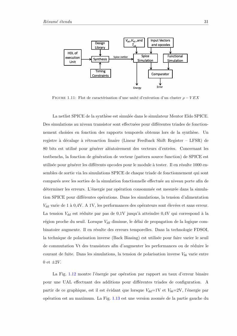
Figure 1.11: Flot de caracterisation d’une unite d’execution d’un cluster ρ− V EX
La netlist SPICE de la synthese est simulee dans le simulateur Mentor Eldo SPICE.
Des simulations au niveau transistor sont effectuees pour differentes triades de fonction-
nement choisies en fonction des rapports temporels obtenus lors de la synthese. Un
registre a decalage a retroaction linaire (Linear Feedback Shift Register – LFSR) de
80 bits est utilise pour generer aleatoirement des vecteurs d’entrees. Concernant les
testbenchs, la fonction de generation de vecteur (pattern source function) de SPICE est
utilisee pour generer les differents opcodes pour le module a tester. Il en resulte 1000 en-
sembles de sortie via les simulations SPICE de chaque triade de fonctionnement qui sont
compares avec les sorties de la simulation fonctionnelle effectuee au niveau porte afin de
determiner les erreurs. L’energie par operation consommee est mesuree dans la simula-
tion SPICE pour differentes operations. Dans les simulations, la tension d’alimentation
Vdd varie de 1 a 0,4V. A 1V, les performances des operateurs sont elevees et sans erreur.
La tension Vdd est reduite par pas de 0,1V jusqu’a atteindre 0,4V qui correspond a la
region proche du seuil. Lorsque Vdd diminue, le delai de propagation de la logique com-
binatoire augmente. Il en resulte des erreurs temporelles. Dans la technologie FDSOI,
la technique de polarisation inverse (Back Biasing) est utilisee pour faire varier le seuil
de commutation Vt des transistors afin d’augmenter les performances ou de reduire le
courant de fuite. Dans les simulations, la tension de polarisation inverse Vbb varie entre
0 et ±2V.
La Fig. 1.12 montre l’energie par operation par rapport au taux d’erreur binaire
pour une UAL effectuant des additions pour differentes triades de configuration. A
partir de ce graphique, est il est evidant que lorsque Vdd=1V et Vbb=2V, l’energie par
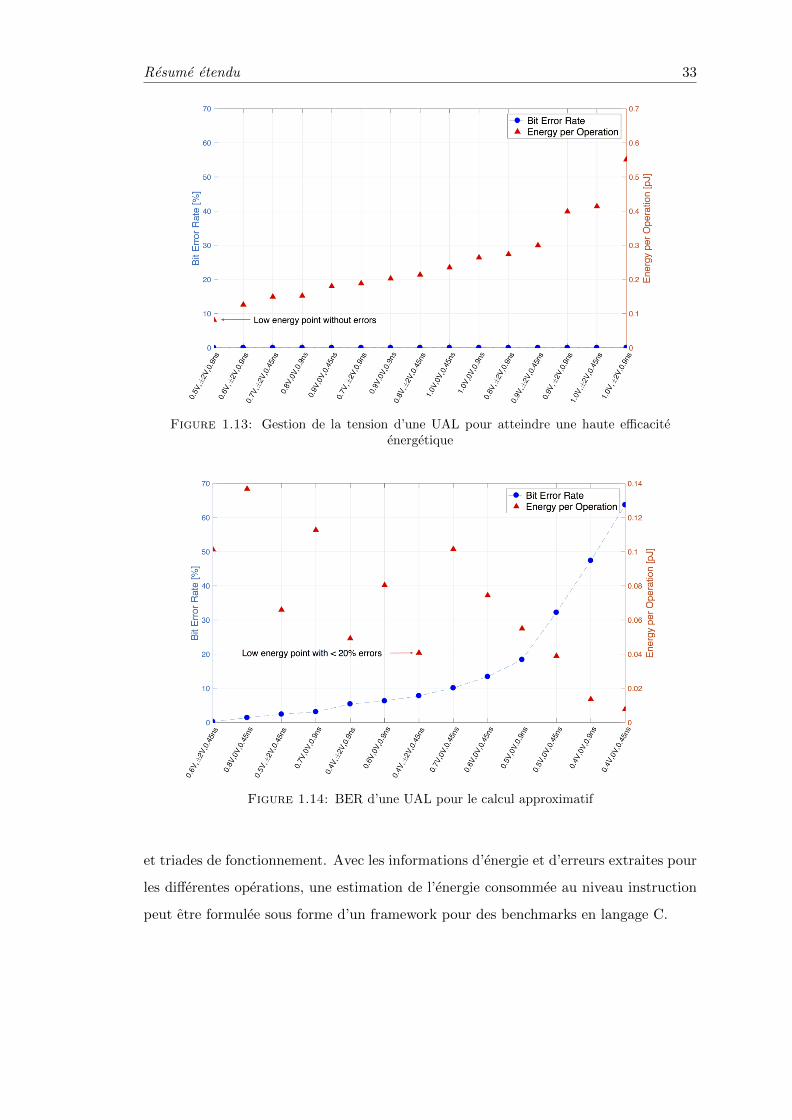
operation est au maximum. La Fig. 1.13 est une version zoomee de la partie gauche du

Resume etendu 32
graphique de la Fig. 1.12. La Fig. 1.13 montre la tendance obtenue par la diminution
de la tension et l’impact engendre par la reduction de l’energie par operation. Lorsque
Vdd=0,5V, l’energie par operation est reduite de 85% sans erreur. La Fig. 1.14 est la
version zoomee de la partie droite de la Fig. 1.12. Pour une application pouvant tolerer
un BER de 10%, Vdd peut etre reduit jusqu’a 0,4V avec une periode d’horloge divisee
par deux afin d’obtenir une efficacite energetique de 93% avec un BER acceptable de
7,8%. Les autres operations de l’UAL montrent des caracteristiques similaires. Comme
montre par ces graphiques, dans la region super-threshold (Vdd de 0,7 a 1V), il n’y a pas
de benefice engendre par la technique de polarisation inverse etant donne que le BER
est le meme pour toutes les triades : sans erreur. Au contraire, dans la region proche
du seuil (Vdd de 0,4 a 0,6V), les benefices de la polarisation inverse sont evidents.
Figure 1.12: Energie consommee en fonction du BER pour une UAL effectuant uneaddition
Les modeles existant de puissance et d’energie pour leur estimation au niveau in-
struction de plateforme VLIW ne sont pas developpes dans le contexte d’alimentation
proche du seuil. Cette limitation reduit la reutilisation de tels modeles pour des ap-
plications comme le traitement d’image et de video, la fouille de donnees, etc., pour
lesquels il y a un interet a configurer l’alimentation proche du seuil afin d’obtenir une
haute efficacite energetique au prix d’erreurs temporelles acceptables et parametrables
par l’utilisateur. La methode de caracterisation proposee est utilisee pour caracteriser le
comportement d’une unite d’execution d’un cluster ρ−V EX pour diverses instructions
Resume etendu 33
Figure 1.13: Gestion de la tension d’une UAL pour atteindre une haute efficaciteenergetique
Figure 1.14: BER d’une UAL pour le calcul approximatif
et triades de fonctionnement. Avec les informations d’energie et d’erreurs extraites pour
les differentes operations, une estimation de l’energie consommee au niveau instruction
peut etre formulee sous forme d’un framework pour des benchmarks en langage C.
Resume etendu 34
1.5.2 Methode proposee pour l’estimation de l’energie au niveau in-
struction
Dans ce travail, nous proposons une methode d’estimation energetique au niveau fonc-
tionnel. La consommation energetique de differentes instructions est estimee en se basant
sur la caracterisation de l’unite d’execution d’un cluster ρ−V EX, detaillee dans la sec-
tion precedente. En general, l’execution d’une instruction apparaıt a differents etages du
pipeline : fetch, decode, execute, et writeback. L’energie consommee par chacun de ces
etages est respectivement notee Efetch, Edecode, Etotexec, Ereg, et Ewriteback. La somme
de toutes ces energies donne l’energie totale consommee pour executer une instruction.
Dans le total d’energie consommee par une instruction, l’etage execute domine par rap-
port aux autres. L’objectif premier de ce travail est d’estimer avec precision l’energie
consommee par l’etage execute pour diverses instructions et avec differentes configu-
rations. Dans la section precedente, la procedure de caracterisation est detaillee pour
l’UAL et le multiplieur d’un cluster ρ − V EX selon differentes configurations. Il y a
au total 73 instructions differentes pour un ρ − V EX. Chaque instruction, selon le
type d’operation, active un certain nombre de blocs dans le cluster. Par exemple, une
instruction peut necessiter deux additions et deux multiplications. Les syllabes (une
operation encodee) 0 et 3 d’une instruction seront allouees pour les additions, et les
syllabes 1 et 2 seront allouees pour les multiplications. A l’aide de la caracterisation
des unites UAL et MUL, l’energie consommee d’une instruction, pour n’importe quelle
configuration de fonctionnement, est determinee par la somme des energies des 4 unites
fonctionnelles. Etant donne que les unites fonctionnelles sont caracterisees pour de nom-
breuses triades de fonctionnement, il est simple d’estimer l’energie pour n’importe quel
benchmark par une simple compilation a travers un compilateur VEX. Cette methode
peut etre facilement adoptee pour estimer la consommation energetique pour differents
processeurs sans avoir besoin de re-caracteriser. Le reste de cette section explique la
procedure d’estimation d’energie pour l’etage execute d’un cluster ρ− V EX.
Pour estimer la consommation energetique au niveau instruction, le programme
benchmark est compile via la chaine d’outils VEX et les fichiers intermediaires .s et .cs.c
sont generes. Le fichier .cs.c contient la macro-declaration de chaque operation VEX, par
exemple ADD, XOR, etc. Dans la section precedente, l’energie par operation est calculee
a partir des simulations SPICE. En connaissant le nombre de fois qu’une operation est

Resume etendu 35
executee il est possible d’estimer l’energie consommee pour n’importe quelle instruction.
En etendant cette methode a toutes les instructions d’un programme, la consomma-
tion energetique totale peut etre estimee. Pour un programme avec P sequence de N
instruction (i1, i2, i3, ..., iN ) ou chaque instruction in contient L differentes operations,
l’estimation energetique de l’unite d’execution peut s’ecrire:
Etot(i) =∑∀k∈L
Eexe(ok)×Mk (1.3)
Eexe(P ) =∑∀n∈N
Etot(in) (1.4)
ou Etot(in) represente l’energie consommee par l’unite d’execution pour executer une
instruction (in). Eexe(ok) est l’energie consommee par une operation (ok), et Mk est le
nombre de fois que l’operation (ok) est executee. L’energie consommee par differentes
operations Eexe(o) est obtenue a travers la phase de caracterisation pour differentes con-
ditions de fonctionnement. De plus, l’Eqn. 1.3 represente l’energie totale consommee
par l’unite d’execution pour une instruction in. L’Eqn. 1.4 represente l’energie totale
consommee par l’unite d’execution pour executer un programme P avec N instructions.
Etant donne que l’on se focalise uniquement sur l’unite d’execution d’un cluster ρ−V EX,
seulement l’energie consommee par cette unite est estimee. En considerant une consom-
mation energetique arbitraire pour les autres modules, l’energie totale consommee par
un cluster ρ− V EX pour executer un programme P peut s’ecrire:
Etotal(P ) = Efetch(P ) + Edecode(P ) + Etotexec(P ) + Ereg(P ) + Ewriteback(P ) (1.5)
ou Efetch(P ), Edecode(P ), Ereg(P ), Ewriteback(P ) representent l’energie consommee pour
les etages fetch, decode, registers, writeback, lors de l’execution du programme considere.
1.5.3 Validation de la methode
La methode d’estimation d’energie est implementee pour un ensemble de benchmarks
ecrit en C. Pour tous les benchmarks, le fichier .cs.c est modifie afin d’augmenter un
compteur pour chaque execution specifique d’une operation. Via les equations Eqn. 1.3
et Eqn. 1.4, l’energie consommee de l’unite d’execution d’un cluster p-Vex est estimee
pour differentes triades de fonctionnement. Les benchmarks choisis sont les plus utilises

Resume etendu 36
Table 1.4: Details des programmes de test
Benchmarks Total Number of Instructions Total number of traces
abs 5 1
find min 41 7
crc8 comp 57 7
crc16 comp 57 7
bphash 60 9
binary search 88 11
fir basic 115 16
calc neigbhour 135 14
dans les applications de mathematiques, traitement du signal et cryptographie, et sont
issus de la suite Mediabench. La Table 1.4 montre la liste des benchmarks ainsi que le
total d’instruction pour chaque programme.
Figure 1.15: Estimation d’energie pour differents benchmarks et pour differents Vdd,Vbb = 0V, et Tclk = 0.9ns
Le fichier .cs.c modifie est execute dans un compilateur C afin d’estimer l’energie
consommee pour differentes triades. La Fig. 1.15 montre l’estimation d’energie pour
l’unite d’execution du cluster ρ − V EX pour chaque programme et pour differentes
valeurs de Vdd allant de 1V a 0,4V sans polarisation inverse. Reduire Vdd de 1V a 0,4V
reduit en moyenne la consommation energetique par un facteur 20. Ce gain significatif
est limite par les erreurs temporelles mis en avant sur le graphique montrant l’energie en
fonction du BER dans la section caracterisation. Cette limitation peut etre compensee
en utilisant de la polarisation inverse pour limiter le BER a une marge acceptable au

Resume etendu 37
Figure 1.16: Estimation d’energie d’une unite d’execution pour differents benchmarkspour differents Vdd, Vbb = 2V, et Tclk = 0.9ns
detriment d’une reduction du gain en energie. La Fig. 1.16 montre l’estimation d’energie
pour chaque application avec un Vbb de 2V. Avec de la polarisation inverse et pour Vdd
a 0,4V, l’energie est reduite en moyenne d’un facteur 11.
Figure 1.17: Estimation d’energie d’une unite d’execution pour differents benchmarkspour differents Vdd, Vbb = 0V, et Tclk = 0.45ns
En plus de la diminution de la tension d’alimentation, une augmentation de la
frequence d’horloge est effectuee pour reduire la periode Tclk de 0,9ns a 0,45ns. Cela
augmente les gains en energie au cout d’une diminution du BER. Pour une periode
d’horloge reduite, les programmes atteignent une reduction energetique d’un facteur 31
pour un Vdd de 0,4V par rapport a 1V. Avec un Vbb de 2V, les erreurs temporelles sont

Resume etendu 38
Figure 1.18: Estimation d’energie d’une unite d’execution pour differents benchmarkspour differents Vdd, Vbb = 2V, et Tclk = 0.45ns
limitees et la consommation energetique est divisee par 10 en moyenne par rapport a
un Vdd de 1V. Le Framework propose permet de comprendre de facon simple le com-
portement de l’unite d’execution d’un cluster ρ − V EX pour differentes triades. Avec
ce Framework, un concepteur peut definir le meilleur compromis entre l’energie et la
precision de calcul pour n’importe quel programme en choisissant, en cours de fonction-
nement, la triade a configurer.
1.6 Conclusion
Dans cette these, un Framework est propose pour gerer les erreurs temporelles et pour es-
timer la consommation energetique des applications tolerantes aux erreurs dans un cadre
de calcul proche du seuil. Dans un environnement ou l’energie est limitee, maintenir un
circuit fonctionnel pour une longue periode est un challenge majeur dans la conception
actuelle de circuit numerique. De nombreuses techniques dites faible consommation sont
explorees a differents niveaux d’abstraction afin d’ameliorer l’efficacite energetique. La
gestion dynamique de l’alimentation est une technique phare permettant d’augmenter
l’efficacite energetique des architectures en reduisant la tension d’alimentation en cours
de fonctionnement. Dans ce travail, nous avons explore le calcul proche du seuil afin
d’ameliorer les gains en energie en reduisant l’alimentation au plus proche du seuil de

Resume etendu 39
commutation des transistors. Reduire la tension d’alimentation rend les circuits plus sen-
sibles aux effets de variabilite et aux erreurs temporelles. Nous avons propose d’utiliser la
technologie FDSOI, qui est de maniere inherente une technologie a faible courant de fuite,
afin de contrer les effets de la variabilite en utilisant la technique de polarisation inverse.
Differentes techniques de gestions des erreurs, comme celle du double echantillonnage,
sont generalement utilisees pour gerer les erreurs. La majorite des techniques basees
sur le double echantillonnage utilisent une fenetre fixe de speculation pour detecter et
corriger les erreurs temporelles. Dans ce travail, nous avons propose l’utilisation d’une
fenetre dynamique de speculation permettant de detecter et de corriger les erreurs tem-
porelles tout en adaptant la tension d’alimentation au plus proche de la tension de seuil.
Nous avons demontre les avantages de cette speculation dynamique via une plateforme
FPGA de Xilinx. Nous avons overclocke des applications de benchmarks au sein du
FPGA au dela de la frequence maximale estimee. De plus, les effets de variabilite ont
ete introduits sur le FPGA en faisant varier sa temperature. Dans ces experimentations,
la methode proposee est capable d’ajuster dynamiquement la frequence d’horloge afin
de contrer les impacts lies a la variabilite et en respectant des marges d’erreurs definies
par l’utilisateur. Nous avons atteint une augmentation de la frequence d’horloge de 71%
avec la methode de speculation dynamique sans erreur, avec un surcout limite de 1,9%
de LUT et 1,7% de registres.
En plus des aspects de detection et de correction des erreurs, ce travail explore
egalement le domaine du calcul approximatif. Dans ce domaine emergeant, les erreurs de
calcul sont deliberement tolerees afin d’atteindre une haute efficacite energetique. Dans
notre methode de speculation dynamique, l’utilisateur peut decider de tolerer un nombre
d’erreurs en specifiant une marge. En fonction d’un niveau de precision a atteindre selon
l’application visee, l’utilisateur peut choisir un compromis entre precision et energie.
En effet, l’utilisateur peut decider en cours de fonctionnement, s’il souhaite une haute
precision ou une haute efficacite energetique en configurant la tension d’alimentation
proche ou loin du seuil. La gestion agressive de la tension (Voltage OverScaling –
VOS) peut etre efficacement appliquee a des applications tolerantes aux erreurs. Ainsi,
nous avons propose un Framework pour modeliser de maniere statistique des operateurs
arithmetiques sous VOS. Le comportement des operateurs alimentes proche du seuil est
different d’un Vdd nominal. Nous avons effectue une etude approfondie de ces operateurs
au niveau transistor afin de caracteriser leur comportement pour du VOS. Les modeles

Resume etendu 40
statistiques peuvent etre utilises au niveau algorithme pour simuler l’effet du VOS afin
de choisir la bonne triade de configuration (Vdd, Vbb et Tclk) pour atteindre une haute
efficacite energetique avec une perte de precision acceptable en fonction de l’application.
Pour etendre le champs d’application du VOS et de la speculation dynamique,
nous avons explore une plateforme reconfigurable via un processeur VLIW. L’unite
d’execution d’un cluster du processeur VLIW ρ−V EX est etudiee. Nous avons propose
un Framework pour caracteriser, evaluer et valider l’estimation energetique de cette unite
pour differentes triades de fonctionnement. L’unite fonctionnelle du cluster ρ − V EX
est caracterisee au niveau transistor afin d’extraire avec precision l’energie consommee
et les erreurs de donnees pour differentes triades. Des simulations au niveau transistor
sont tres longues meme pour un programme simple. Ainsi, nous avons propose une
estimation d’energie au niveau instruction par une simple compilation en C d’un pro-
gramme. De ce fait, nous pouvons estimer la consommation d’energie d’un programme
pour differentes configurations tres rapidement a partir d’une caracterisation au niveau
transistor. Nous avons egalement propose une procedure de validation alternative pour
s’assurer de la precision de l’estimation energetique en comparant avec une simulation
complete SPICE des benchmarks. Dans ce Framework nous avons atteint une precision
d’estimation d’energie ayant seulement 2% d’erreurs en moyenne.
1.7 Perspective
Un des principaux challenges dans la conception de circuit numerique est d’atteindre
une haute efficacite energetique pour un cout minimum en terme de surface de silicium
tout en fournissant un compromis acceptable entre precision et performance du circuit.
Etant donnee la dependance quadratique entre la consommation d’energie et la ten-
sion d’alimentation, reduire Vdd mene a une meilleure efficacite energetique. Une simple
observation des differentes technologies CMOS sur les dix dernieres annees montre la
tendance a la diminution de la tension d’alimentation. Dans la region proche du seuil,
la latence et l’energie sont fortement lineaire par rapport a Vdd. Utiliser des transis-
tors dans cette region offre un meilleur controle sur le compromis energie-erreur. La
technologie FDSOI est utilisee pour ameliorer les benefices de l’alimentation proche du
seuil. Cependant, l’impact de la variabilite et les erreurs temporelles l’emportent sur les

Resume etendu 41
benefices produits par cette baisse de la tension d’alimentation. Dans cette these, nous
avons adresse cette problematique via trois contributions.
Figure 1.19: Perspective generale de la these
La Fig. 1.19 mets en lumiere la perspective de cette these. On considere un clus-
ter VLIW avec ses differents etages pipelines : chargement d’instruction (instruction
fetch), decodage d’instruction (decode), l’etape d’execution est representee par une unite
fonctionnelle (FU), des files de registres (register files) et un bloc memoire (memory).
Dans une execution classique, les instructions sont chargees et decodees par les etages
fetch et decode. Les differentes operations de chaque instruction sont executees dans les
FU en paralleles. La sortie est sauvegardee dans la file de registres et la memoire. Afin
d’atteindre une haute efficacite energetique, la tension de chaque FU peut etre diminuee.
La diminution du Vdd peut generer des erreurs qui peuvent etre gerees en utilisant les
methodes expliquees dans le Chapitre 3. Dans le Chapitre 3, les limitations des tech-
niques sont discutees en detail. Ainsi, le besoin pour une approche unifiee pour gerer les
erreurs est necessaire afin d’atteindre un compromis energie-erreurs.
La Fig. 1.19 montre cette approche unifiee permettant de gerer les erreurs tem-
porelles dans le contexte d’alimentation proche du seuil et de calcul approximatif pour
des applications tolerantes aux fautes. Les FU sont monitores en utilisant la methode
proposee de speculation dynamique utilisant une boucle de retour. Le principal avantage
de la methode proposee est de fournir une tolerance aux erreurs adaptable en fonction

Resume etendu 42
d’une marge d’erreur definissable par l’utilisateur. A l’aide de la mesure temps reel de la
marge temporelle disponible, la methode proposee peut predire les possibilites d’erreurs.
En cas de besoin, un mecanisme de prevention peut etre mise en oeuvre afin de configurer
la triade d’operation. En fonction de la marge d’erreur configuree par l’utilisateur, les
erreurs peuvent etre detectees et corrigees ou ignorees en cours de fonctionnement selon
le besoin des differentes applications. La boucle de contre-reaction effectue l’adaptation
de la frequence d’horloge ou de la tension d’alimentation lorsqu’il y a besoin d’augmenter
l’efficacite energetique ou les performances. La methode proposee fournit une flexibilite
pour le concepteur en fonction des besoins.
Dans ces travaux, le comportement des differents operateurs arithmetiques sont
etudies pour differentes triades de fonctionnement. Cela fournit un apercu detaille de
la generation et de la propagation dans les differents operateurs. A l’aide de cette
etude, la speculation dynamique est utilisee tel qu’illustree en Fig. 1.19 afin de reduire
l’energie dans les operateurs arithmetiques en temps reel. Afin de facilement compren-
dre differents compromis possibles, un framework d’estimation d’energie est proposee
pouvant simuler n’importe quel programme de test via un compilateur C afin de fournir
l’estimation energetique selon differentes triades de fonctionnement. Cela fournit une
aide au developpeur pour comprendre les benefices et les impacts, ainsi que les couts
pour atteindre le meilleur compromis entre energie et erreurs.

Chapter 2
Introduction
Advancement in CMOS (Complementary Metal-Oxide-Silicon) IC (Integrated Chip)
technology has improved the way in which integrated circuits are designed and fab-
ricated over decades. Gordon Moore predicted in 1965, that the number of components
that could be incorporated per integrated circuit will double every two years [9]. Scaling
down the size of transistors from micrometers to few nanometers has given the capa-
bility to place more and more tinier transistors in a unit of chip area that upheld the
Moore’s law over the years. Scaling feature size expanded the functional capability
of ICs multi-fold by accommodating more components. Components once placed on
Printed Circuits Board (PCB) along with processor are now packed inside single chip
as popularly know as System-on Chip (SoC). Prime requirements in any IC design is
to increase the performance (by reducing gate delay) and to reduce power consumption
and area (silicon footprint). As per general scaling rule, feature size scaled down by a
factor of K results in reduction of gate delay by K, power by K2, and energy by K3.
This makes scaling an important technique to achieve all the three prime requirements of
IC designing. In 2007, International Technology Road-map for Semiconductors (ITRS)
highlighted slowdown in the trend of feature size scaling and forecasted that the scaling
trend of CMOS will come to a halt at 22nm [10]. Various challenges like Physical, Ma-
terial, Power-thermal, Technological, and Economical that hinder the scaling trend have
been discussed in [11]. Out of the listed challenges, physical limitations due to incre-
mental tunneling and leakage currents because of smaller channel length pose a major
challenge to scaling of CMOS devices. ITRS stated in 2011, ”One of the key problems
that designers face due to further shrinking of features sizes is the increasing variability
43

Chapter 1. Introduction 44
of design-related parameters, resulting either from variations of fabrication parameters
or from the intrinsic atomistic nature” [12]. Also, to improve energy efficiency supply
voltage (Vdd) scaling [1] is employed in most of the Ultra-Low Power (ULP) designs.
However reduction in Vdd augments the impact of variability in sub-nanometer designs.
2.1 Variability in CMOS
Variability is defined as the discrepancies in the functioning of circuits due to variation in
Process, Voltage and Temperature (PVT) of the devices. In the following sub-sections,
each of these variations is discussed briefly.
2.1.1 Process variations
Various imperfections in transistor manufacturing process that lead to process variations
are listed in [13].
• Variations in the critical dimension of devices happen due to imperfections in
fabrication technology because of higher wavelength light is used in lithography to
make smaller size transistors.
• In a doped channel, impurity atoms placed by dopant implantation randomly
fluctuate causing variations in threshold voltage of the devices. This effect is
called Random Dopant Fluctuation (RDF).
• Variations in gate oxide thickness (TOX) induces variations in threshold voltage.
This effect is more pronounced in technologies of 30nm and below.
Process variations are broadly classified into global and local based on the cause
and impact of the variations. Global variations impact all the transistors equally due to
discrepancies in parameters like oxide thickness and dopant concentration. In contrast,
local variations impacts are different for different transistors.

Chapter 1. Introduction 45
2.1.2 Voltage variations
Supply voltage Vdd plays an important role in proper functioning of digital circuits.
Reduction in Vdd results in increased gate delay tp, which in turn affects the performance
of the digital circuits
tp =Vdd.Cload
k(Vdd − Vt)n(2.1)
where Cload is the load capacitance, Vt is the threshold voltage, k and n are technology
parameter that determines drain current characteristics. For a long-channel device, value
of n is 2 and for a short-channel device 1 ≤ n < 2 . Supply voltage variations are mainly
caused by IR drop and di/dt noise [13].
• IR drop, is due to the voltage drop because of the resistance of interconnects.
• di/dt noise is due to the voltage drop because of time-varying current drawn by
the inductance of the package leads.
Apart from the above-mentioned voltage variations, this impact is also seen in the
controlled supply voltage scaling implemented in the digital circuit to reduce the energy
consumption of the circuit.
2.1.3 Temperature variations
As the chip density getting doubled every two years, temperature of the device increases
proportionally to the chip density. For every 10◦C increase in the operating temper-
ature, failure rate roughly doubles [14] due to reduced carrier mobility and increased
interconnect resistance. In general, gate delay tp increases with increasing temperature
and decreasing Vdd. However, at low supply voltages, tp decreases with increasing tem-
perature known as inverted temperature dependence (ITD). Due to ITD it becomes really
difficult to analytically determine the impact of temperature variations on tp. Effect of
ITD is discussed in [15].
• Due to ITD, it becomes hard to define corners by independently varying Vdd and
Vt.
• It becomes more difficult to find short paths which cause hold time violations.
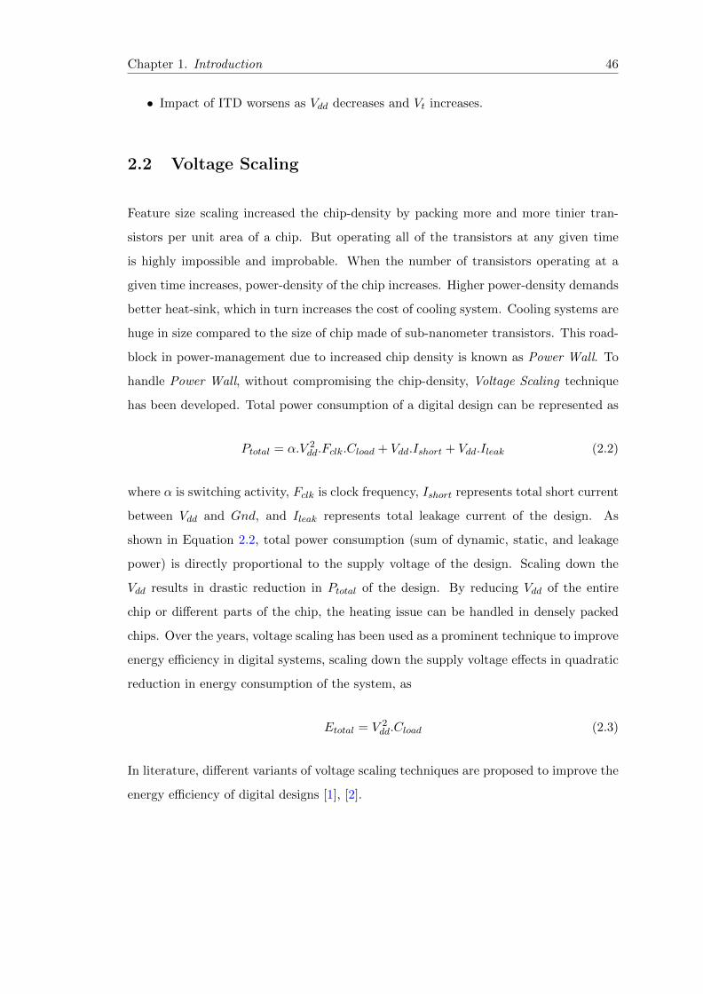
Chapter 1. Introduction 46
• Impact of ITD worsens as Vdd decreases and Vt increases.
2.2 Voltage Scaling
Feature size scaling increased the chip-density by packing more and more tinier tran-
sistors per unit area of a chip. But operating all of the transistors at any given time
is highly impossible and improbable. When the number of transistors operating at a
given time increases, power-density of the chip increases. Higher power-density demands
better heat-sink, which in turn increases the cost of cooling system. Cooling systems are
huge in size compared to the size of chip made of sub-nanometer transistors. This road-
block in power-management due to increased chip density is known as Power Wall. To
handle Power Wall, without compromising the chip-density, Voltage Scaling technique
has been developed. Total power consumption of a digital design can be represented as
Ptotal = α.V 2dd.Fclk.Cload + Vdd.Ishort + Vdd.Ileak (2.2)
where α is switching activity, Fclk is clock frequency, Ishort represents total short current
between Vdd and Gnd, and Ileak represents total leakage current of the design. As
shown in Equation 2.2, total power consumption (sum of dynamic, static, and leakage
power) is directly proportional to the supply voltage of the design. Scaling down the
Vdd results in drastic reduction in Ptotal of the design. By reducing Vdd of the entire
chip or different parts of the chip, the heating issue can be handled in densely packed
chips. Over the years, voltage scaling has been used as a prominent technique to improve
energy efficiency in digital systems, scaling down the supply voltage effects in quadratic
reduction in energy consumption of the system, as
Etotal = V 2dd.Cload (2.3)
In literature, different variants of voltage scaling techniques are proposed to improve the
energy efficiency of digital designs [1], [2].
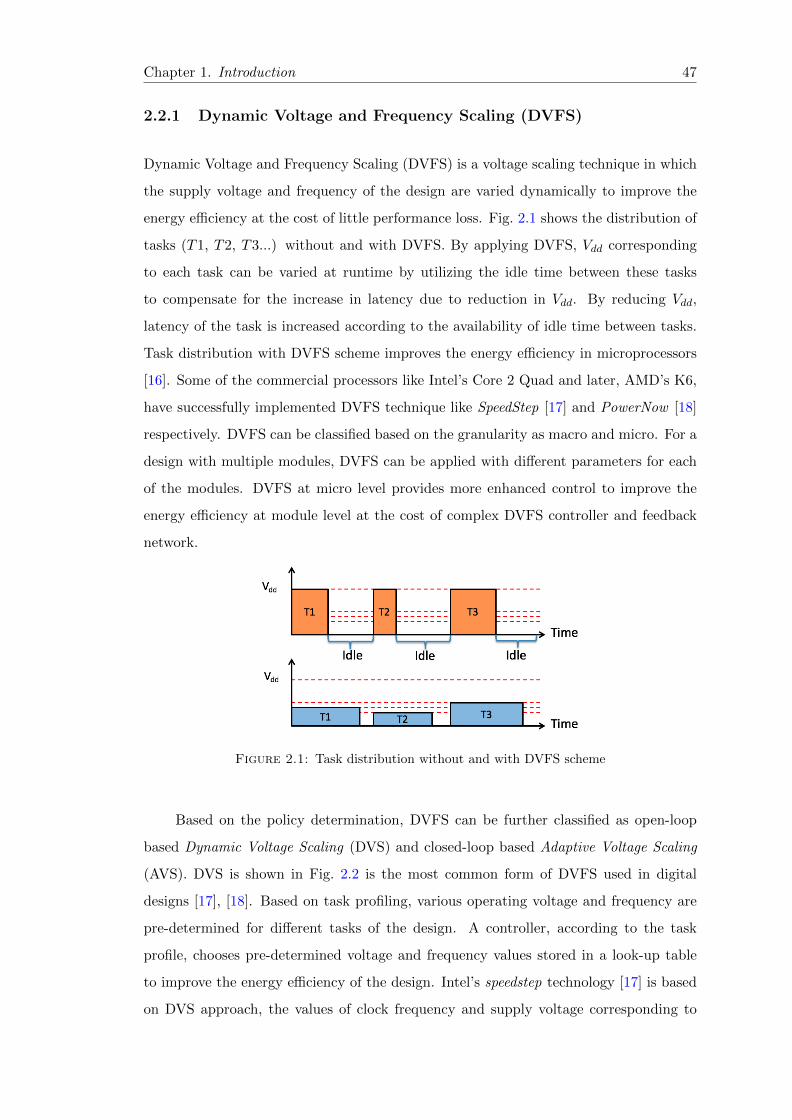
Chapter 1. Introduction 47
2.2.1 Dynamic Voltage and Frequency Scaling (DVFS)
Dynamic Voltage and Frequency Scaling (DVFS) is a voltage scaling technique in which
the supply voltage and frequency of the design are varied dynamically to improve the
energy efficiency at the cost of little performance loss. Fig. 2.1 shows the distribution of
tasks (T1, T2, T3...) without and with DVFS. By applying DVFS, Vdd corresponding
to each task can be varied at runtime by utilizing the idle time between these tasks
to compensate for the increase in latency due to reduction in Vdd. By reducing Vdd,
latency of the task is increased according to the availability of idle time between tasks.
Task distribution with DVFS scheme improves the energy efficiency in microprocessors
[16]. Some of the commercial processors like Intel’s Core 2 Quad and later, AMD’s K6,
have successfully implemented DVFS technique like SpeedStep [17] and PowerNow [18]
respectively. DVFS can be classified based on the granularity as macro and micro. For a
design with multiple modules, DVFS can be applied with different parameters for each
of the modules. DVFS at micro level provides more enhanced control to improve the
energy efficiency at module level at the cost of complex DVFS controller and feedback
network.
Figure 2.1: Task distribution without and with DVFS scheme
Based on the policy determination, DVFS can be further classified as open-loop
based Dynamic Voltage Scaling (DVS) and closed-loop based Adaptive Voltage Scaling
(AVS). DVS is shown in Fig. 2.2 is the most common form of DVFS used in digital
designs [17], [18]. Based on task profiling, various operating voltage and frequency are
pre-determined for different tasks of the design. A controller, according to the task
profile, chooses pre-determined voltage and frequency values stored in a look-up table
to improve the energy efficiency of the design. Intel’s speedstep technology [17] is based
on DVS approach, the values of clock frequency and supply voltage corresponding to
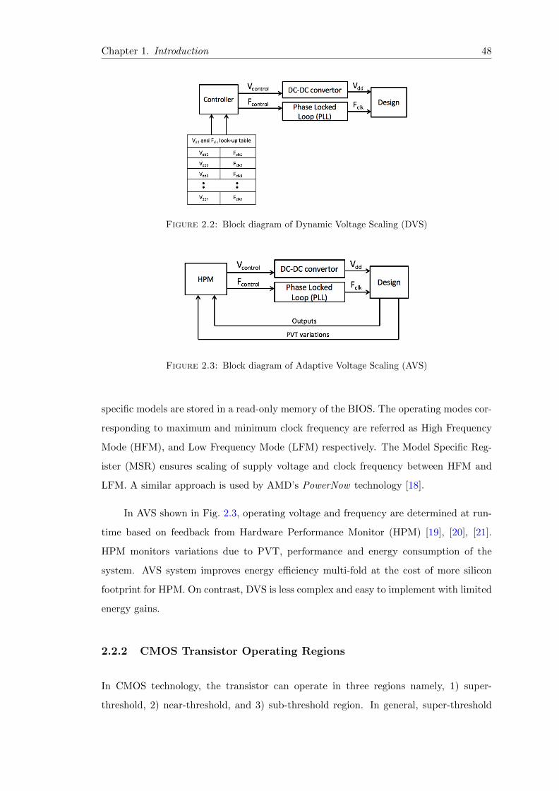
Chapter 1. Introduction 48
Figure 2.2: Block diagram of Dynamic Voltage Scaling (DVS)
Figure 2.3: Block diagram of Adaptive Voltage Scaling (AVS)
specific models are stored in a read-only memory of the BIOS. The operating modes cor-
responding to maximum and minimum clock frequency are referred as High Frequency
Mode (HFM), and Low Frequency Mode (LFM) respectively. The Model Specific Reg-
ister (MSR) ensures scaling of supply voltage and clock frequency between HFM and
LFM. A similar approach is used by AMD’s PowerNow technology [18].
In AVS shown in Fig. 2.3, operating voltage and frequency are determined at run-
time based on feedback from Hardware Performance Monitor (HPM) [19], [20], [21].
HPM monitors variations due to PVT, performance and energy consumption of the
system. AVS system improves energy efficiency multi-fold at the cost of more silicon
footprint for HPM. On contrast, DVS is less complex and easy to implement with limited
energy gains.
2.2.2 CMOS Transistor Operating Regions
In CMOS technology, the transistor can operate in three regions namely, 1) super-
threshold, 2) near-threshold, and 3) sub-threshold region. In general, super-threshold
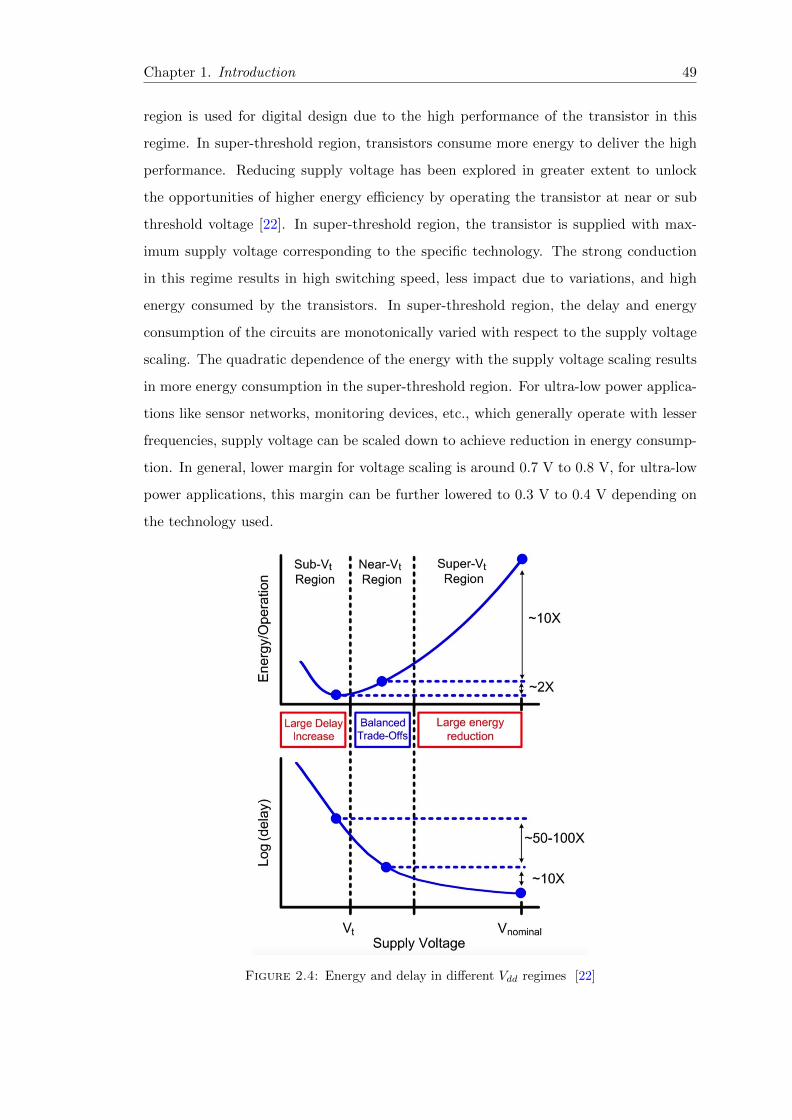
Chapter 1. Introduction 49
region is used for digital design due to the high performance of the transistor in this
regime. In super-threshold region, transistors consume more energy to deliver the high
performance. Reducing supply voltage has been explored in greater extent to unlock
the opportunities of higher energy efficiency by operating the transistor at near or sub
threshold voltage [22]. In super-threshold region, the transistor is supplied with max-
imum supply voltage corresponding to the specific technology. The strong conduction
in this regime results in high switching speed, less impact due to variations, and high
energy consumed by the transistors. In super-threshold region, the delay and energy
consumption of the circuits are monotonically varied with respect to the supply voltage
scaling. The quadratic dependence of the energy with the supply voltage scaling results
in more energy consumption in the super-threshold region. For ultra-low power applica-
tions like sensor networks, monitoring devices, etc., which generally operate with lesser
frequencies, supply voltage can be scaled down to achieve reduction in energy consump-
tion. In general, lower margin for voltage scaling is around 0.7 V to 0.8 V, for ultra-low
power applications, this margin can be further lowered to 0.3 V to 0.4 V depending on
the technology used.
Figure 2.4: Energy and delay in different Vdd regimes [22]

Chapter 1. Introduction 50
2.2.2.1 Sub-Threshold Region
In sub-threshold region (STR), the supply voltage of the transistor is slightly lesser
than the threshold voltage of the transistor. Though in general terms it is said that
the transistor is in cut-off mode, there is a little sub-threshold current flowing through
the channel. In sub-threshold region, the drain current Id decreases exponentially, thus
a non-zero gate voltage that is less than Vt will still produce a drain current that is
larger than the off current( Ioff = Id when Vgs = 0V). The ratio of Ion/Ioff knows as
sub-threshold slope determines the speed of the transistor. Steeper the slope, faster the
transition between OFF and ON logic levels. Though the ratio of Ion/Ioff is positive
in the sub-threshold region, a lower Ion/Ioff ratio can lead to functional problems [23].
Also, the transient behavior is much slower because the on-current in this region is orders
of magnitude less than in strong inversion (super-threshold) region. In sub-threshold
region, delay increases exponentially when the supply voltage is scaled down. Since the
leakage energy is linear with the circuit delay, the fraction of leakage energy increases
with the supply voltage scaling. Fig. 2.4 shows the plots of energy and delay vs. supply
voltage in different operating regions. In sub-threshold region, energy per operation is
12× less than the super-threshold region. On the other hand, delay increases by 50-
100×. Also, the leakage energy dominates the benefits from supply voltage scaling in
Sub-Vt region.
2.2.2.2 Near-Threshold Region
In near-threshold region (NTR), the supply voltage of the transistor is slightly more
than the threshold voltage of the transistor. In this region both delay and energy are
roughly linear with the supply voltage, as shown in Fig. 2.4. The Ion/Ioff ratio is more
when compared to the sub-threshold region, which improves the speed and minimizes the
leakage. Due to the reduced supply voltage, the circuits operating in NTR can achieve
a 10× reduction in energy per operation at the cost of the same magnitude of reduction
in operating frequency. As a result of reduced energy per operation and operating
frequency, more cores can be operated in the estimated power budget. Parallelism in the
execution of the application can be used to reduce the effect of the frequency degradation
in the near-threshold regime [24]. Another issue is that sub- and near-threshold designs
are more sensitive to variations due to RDF [25]. In [26] and [27], it is shown that

Chapter 1. Introduction 51
Silicon on Insulator (SOI) technology is highly immune to RDF variations because the
high-k dielectric reduces the gate leakage currents and good channel electrostatic control
diminishes the drain leakage currents.
2.3 FDSOI Technology
Fully Depleted Silicon On Insulator (FDSOI) is a planar CMOS based on SOI technology
[28], [29]. To improve energy efficiency different methods like DVFS, Dynamic Vt control,
etc. are developed. But due to the limitations of Bulk CMOS technology, all these
techniques under performed than their maximum potential. To outweigh the benefits of
low power techniques, FDSOI technology has been developed. In Bulk CMOS, voltage
scaling trend slowed, because scaling Vdd demands scaling of Vt to maintain noise margin.
Scaling Vt is limited due to high leakage current in bulk CMOS. This, in turn, limits Vdd
scaling. Fig. 2.5, shows the cross-section view of Bulk versus FDSOI device. Unlike Bulk,
in FDSOI there is a thin Buried Oxide (BOX) layer between body and substrate of the
device. BOX layer confines charge movement to the thin channel which makes FDSOI
an intrinsically low leakage technology. Thin BOX layer reduces junction capacitance
between source/drain and substrate, thus total dynamic power is lowered. On the other
hand, BOX layer isolates the body from the base substrate causing floating body major
limitation in SOI technologies. The floating body can accumulate charge over time,
which causes variation in threshold voltage of the device. In FDSOI, floating body
problem is addressed by removing dopants from the channel. Also, the undoped channel
makes it fully depleted and reduces the effect of RDF.
FDSOI devices are in general classified as Low Vt (LVT) and Regular Vt (RVT).
Low Vt devices are constructed on Flip Well, meaning PMOS on P-well and NMOS on
N-well. Regular Vt devices are constructed on Conventional Well, with PMOS on N-well
and NMOS on P-well. LVT devices with Forward Body-Bias (FBB) provides boost to
performance by lowering Vt of the device. Data from ST-Microelectronics shows, in
near-threshold regime (Vdd = 0.4V ), 1V FBB provides 120% boost to performance when
compared to no body-biasing. On the other hand 18% performance boost in super-
threshold regime (Vdd = 1V ). RVT devices with Reverse Body-Bias (RBB) reduces
leakage current by increasing Vt of the device. This makes FDSOI with body-biasing a
favourable candidate for near-threshold computing [30].
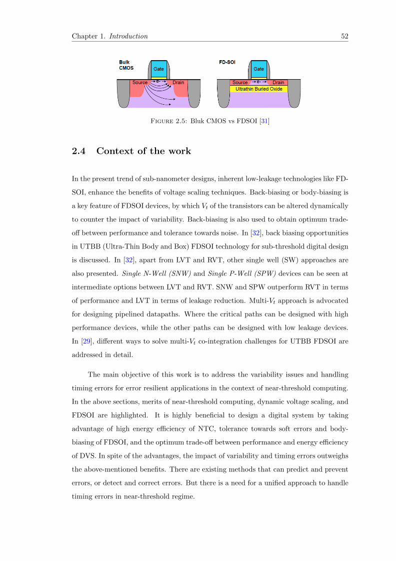
Chapter 1. Introduction 52
Figure 2.5: Bluk CMOS vs FDSOI [31]
2.4 Context of the work
In the present trend of sub-nanometer designs, inherent low-leakage technologies like FD-
SOI, enhance the benefits of voltage scaling techniques. Back-biasing or body-biasing is
a key feature of FDSOI devices, by which Vt of the transistors can be altered dynamically
to counter the impact of variability. Back-biasing is also used to obtain optimum trade-
off between performance and tolerance towards noise. In [32], back biasing opportunities
in UTBB (Ultra-Thin Body and Box) FDSOI technology for sub-threshold digital design
is discussed. In [32], apart from LVT and RVT, other single well (SW) approaches are
also presented. Single N-Well (SNW) and Single P-Well (SPW) devices can be seen at
intermediate options between LVT and RVT. SNW and SPW outperform RVT in terms
of performance and LVT in terms of leakage reduction. Multi-Vt approach is advocated
for designing pipelined datapaths. Where the critical paths can be designed with high
performance devices, while the other paths can be designed with low leakage devices.
In [29], different ways to solve multi-Vt co-integration challenges for UTBB FDSOI are
addressed in detail.
The main objective of this work is to address the variability issues and handling
timing errors for error resilient applications in the context of near-threshold computing.
In the above sections, merits of near-threshold computing, dynamic voltage scaling, and
FDSOI are highlighted. It is highly beneficial to design a digital system by taking
advantage of high energy efficiency of NTC, tolerance towards soft errors and body-
biasing of FDSOI, and the optimum trade-off between performance and energy efficiency
of DVS. In spite of the advantages, the impact of variability and timing errors outweighs
the above-mentioned benefits. There are existing methods that can predict and prevent
errors, or detect and correct errors. But there is a need for a unified approach to handle
timing errors in near-threshold regime.
Chapter 1. Introduction 53
In this thesis, dynamic speculation based error detection and correction is explored
in the context of adaptive overscaling. Apart from error detection and correction, some
errors can also be tolerated, or in other words, circuits can be pushed beyond their limits
to compute incorrectly to achieve higher energy efficiency. It involves extensive study
of design at gate level to understand the behaviour of gates under overscaling of supply
voltage, bias voltage and clock frequency (collectively called as operating triads). A
bottom-up approach is taken: by studying trends of energy vs error of basic arithmetic
operator at gate level to architectures like VLIW (Very Long Instruction Word) proces-
sors with multiple arithmetic operators. Based on the profiling of arithmetic operators,
tool flow to estimate energy and error metrics for different operating triads is proposed.
A model has been developed for the arithmetic operators to represent the behaviour of
the operators for different variability impacts. This model can be used for approximate
computing of error resilient applications that can tolerate acceptable margin of errors.
This method is further explored for execution unit of ρ−V EX VLIW processor. Based
on the study, it is possible to give a quick estimation of energy and error metrics of a
benchmark by a simple compilation of a C program.
In the context of voltage scaling and impact of variability in sub-nanometer designs,
the prime objectives of this thesis work are to address the following
• adaptive error detection and correction scheme for Dynamic Voltage Scaling
• handling timing errors at near-threshold regime to optimize energy efficiency and
performance trade-offs
• extending the near-threshold and error handling methods for VLIW systems.
2.5 Contributions
The contributions of this thesis work are as follows.
1. A dynamic speculation based adaptive overclocking and error correction for pipeline
logic path is proposed. Based on slack measurement and shadow register principle,
this method can identify the opportunity to overclock the system dynamically, and
at the same time can respond to variability effects by underclocking the system

Chapter 1. Introduction 54
based on dynamic speculation. If there are timing errors due to variability effects,
inbuilt correction mechanism handles the errors without executing the instruction
again. Unlike Razor methods, additional buffers are not required for shorter logic
paths. Proof of concept is developed using a Xilinx Virtex-7 FPGA. Results show
that a maximum of 71% overclocking is achieved with a limited area overhead.
2. Energy efficiency and accuracy of different adder and multiplier configurations are
characterized using several operating triads. A framework has been formulated
to model the statistical behaviour of arithmetic operators subjected to voltage
overscaling that can be used for approximate computing at the algorithmic level.
Simulation results show that a maximum of 89% energy reduction is achieved at
the tolerable output bit error rate of 20%.
3. A framework is proposed to estimate the functional level energy consumption of
VLIW architecture. Functional Units (FU) of the VLIW are characterized for
different operating triads. An estimation tool-flow has been developed to analyze
benchmark programs and quickly estimate energy and error metrics for different
operating conditions. Quick estimation is possible by simple C compilation of
benchmark programs using VEX and C compiler. This estimation can be used to
configure the operating triads dynamically to achieve a better trade-off between
energy efficiency and accuracy of the computing. Proof of concept is developed
with ρ−V EX VLIW processor based on the proposed framework. Execution unit
of ρ − V EX VLIW processor is characterized for different operating triads and
functional level energy consumption is estimated using the proposed framework.
2.6 Organization of the Thesis
The thesis is organized as follows. Chapter 3 discusses timing errors and methods to
handle errors. Error handling methods are reviewed briefly under the classification of (1)
Predict and Prevent errors, (2) Detect and Correct errors, and (3) Accept and Living
with errors. Advantages and limitations of the existing error handling methods are
explained.
In Chapter 4, impact of overclocking in FPGA is discussed with experimental re-
sults. Double sampling and slack measurement methods are explained as the basis for
Chapter 1. Introduction 55
the contribution later described in the chapter. Proposed Dynamic Speculation Window
architecture and Adaptive Over/Under-Clocking feedback loop are explained in detail.
FPGA implementation of the proposed method and results are further explained to high-
light the advantages of this method. At last, some of the related works are compared
and contrasted with the proposed method.
In Chapter 5, approximate computing is introduced, and some of the existing ap-
proximate arithmetic operators are discussed. Later in the chapter, characterization of
arithmetic operators and behaviour of arithmetic operators in near-threshold regime are
explained. Rest of the chapter deals with modelling of approximate arithmetic opera-
tors based on the characterization of energy and error metrics. Experimental results on
benchmarks are discussed in detail to validate the proposed methodology.
In Chapter 6, basic introduction to ρ − V EX VLIW processor is given as the
basis for the contribution. Existing methodologies to estimate instruction level energy
in VLIW are discussed. Later in the chapter, characterization of functional units for
different operating triads and the proposed energy estimation framework along with
validation procedure of the proposed energy estimation method are explained. As proof
of concept, energy and error estimation in ρ−V EX processor is discussed based on the
proposed framework. Experimental setup and estimation tool-flow are explained and
results are discussed.
The thesis concludes with Chapter 7 by collating the inferences derived from the
previous chapters. An overall picture of energy efficiency versus error tolerance in the
context of variability impacts and handling timing errors in design based on Near-
Threshold computing, Approximate Computing, Dynamic Voltage Scaling, and FDSOI
is provided. Finally, some perspectives on future work are also outlined.


Chapter 3
Handling Variability and Timing
errors
Variation in process, voltage, and temperature of CMOS technology results in unfaithful
computation. In Chapter 2, variability in CMOS was introduced. In literature, differ-
ent methods are proposed to mitigate variability at technology level, design level, and
software level [33]. Errors due to variability effects are broadly classified as Hard errors
and Soft errors. Hard errors are caused by defects in design or process of the circuit.
These errors are repetitive in nature and make the circuit fail in the same manner for a
given design and process parameters. Soft errors are caused by striking of physical par-
ticles resulting in data corruption. Soft errors are most commonly observed in memory
components, resulting in invalid data being read or processed. But soft errors in FP-
GAs may change the functionality of the programmed FPGA and result in catastrophic
failures. Impact of variability in voltage scaling leads to hard errors known as Timing er-
rors and increases soft error vulnerability. As shown in Fig. 3.1, digital designs are time
constrained with an acceptable positive slack to strike an optimum balance between per-
formance and variability effects. When a design is exposed to variability effects, increase
in propagation delay results in timing failure. The operating frequency of the design has
to be reduced to lower the impact of variability at the cost of reduced throughput. The
impact of variability is more severe in designs with lower-power techniques like DVS,
AVS, etc.
57

Chapter 2. Handling Variability and Timing errors 58
Figure 3.1: Timing errors due to the variability effects
Figure 3.2: Taxonomy of timing error tolerance at different abstractions [33]

Chapter 2. Handling Variability and Timing errors 59
3.1 Handling Errors
As the supply voltage of the design gets scaled down, the failure rate keeps increasing,
which demands reliable and fault-tolerant systems that can work faithfully with above-
mentioned low-power techniques. Fig. 3.2 shows taxonomy of timing error tolerance
at different stages of abstraction. Handling error can be performed in three different
dimensions:
• Predicting and Preventing Errors,
• Detecting and Correcting Errors,
• Accepting and Living with Errors.
Above dimensions of handling errors are applied at circuit, architecture, software,
and application levels. This work primarily targets handling errors at circuit and ar-
chitecture levels. Most common way of handling the error is by predicting the error,
thereby preventing it by employing necessary safeguards. For example, designing a cir-
cuit with large positive slack to handle timing errors falls under this category. This way
of handling errors is more optimistic and takes a toll on the performance of the circuit.
In the past few years, the trend is to detect and correct errors rather than predicting
and preventing errors. Methods like double sampling popularized this concept [4]. By
pushing the performance of the design to point of first failure (POFF) thereby improving
the energy efficiency. When an error is detected, error correction mechanism is invoked
to correct the errors at the cost of reduced performance. These methods demand ad-
ditional hardware to detect and correct errors. Finally, in the era of IoT (Internet of
Things), accepting and living with errors is the trend of the day. To improve energy
efficiency, operating constraints of the circuit are pushed beyond the limits thereby de-
liberately allowing errors to happen and living with those errors up to an acceptable
margin. Approximate Computing or Stochastic Computing for error resilient applica-
tions exhibit this dimension of handling or living with errors. Based on the application,
design environment, and end-user requirements, error handling techniques are employed.
In the following sections, some of the existing error handling techniques under each
dimension are discussed.
Chapter 2. Handling Variability and Timing errors 60
3.2 Predicting and Preventing Errors
Predicting and Preventing Errors is a class of error detecting method in which the timing
errors are predicted using additional hardware and preventive measures are taken to
avoid those errors. Following sub-sections explain the techniques used in this class of
error detection methods.
3.2.1 Critical Path Emulator
In [1], an error prediction and prevention scheme based on critical path emulation has
been proposed. Fig. 3.3 shows the speed detector which contains three logic paths
constrained between registers. The three logic paths are, 1) replica of the critical path
of the circuit (CP ), 2) same critical path with 3% additional delay (CP+), and 3)
the reference path. A Test Data Generator emits test pattern and the output data
comparator matches the data from all the three logic paths. As the reference path
always outputs correct data even at the low VDD, outputs from the other two paths are
compared with reference path. When both the CP and CP+ are wrong, then the supply
voltage is increased, if both the CP and CP+ are correct, then the supply voltage is
decreased. The supply voltage is left unaltered when only CP is correct and CP+ is
wrong. This method needs additional hardware to generate and compare the test data.
Also, this method can not be used for reconfigurable architectures where the critical
path changes based on the functionality of the design.
3.2.2 Canary Flip-Flops
Canary Flip-Flops are used in voltage scaling methods to observe the proximity of timing
errors due to the effect of scaling the supply voltage. It is a common practice to reduce
the Vdd of a datapath during standby state (inactivity state in which supply voltage is
lowered to required minimum retention potential). Registers and other storage elements
are very sensitive to voltage scaling. When the Vdd is reduced below the data retention
potential of the registers, data stored in the registers get corrupted. Different variability
effects directly impact Vdd and cause sudden sags in the supply voltage. To predict
and prevent such errors in pipelined datapaths, canary flip-flops are used along with
datapath registers [34]. Fig. 3.4 shows the schematic of canary based error prediction

Chapter 2. Handling Variability and Timing errors 61
Figure 3.3: Critical Path Emulation based error detection [1]
and prevention of errors. Canary Flip-Flops are designed to fail at higher Vdd compared
to the registers in the datapath pipeline during standby mode. As shown in Fig. 3.4,
Canary Flip-Flops can also be designed like Razor methods [35] with an additional delay
before the shadow FF. Unlike Razor, where the error is detected and corrected, Canary
FFs predict and prevent timing errors. When Vdd is scaled below the safe margin, canary
flip-flops fail before the pipeline registers and send an alert signal to prevent the failure in
the circuit. Canary flip-flops are designed to fail at higher Vdd by proper sizing of master-
slave flip-flops (MSFF) or linear feedback flip-flops (LFBFF). A closed-loop control is
used to sense the feedback from the canary flip-flops and control the standby voltage to
prevent corruption of data in pipeline registers. Canary flip-flops with different failure
voltages, help to identify large process variations within the die, thereby Vdd and Vt
variations can be circumvented. Based on the design profiling, the user determines the
granularity and placement of canary flip-flops. Unlike Razor, Canary logic does not need
shadow clock and dedicated clock tree for shadow clock. Though this method offers a
safe way to scale the standby voltage, the usability of this method is limited to circuits
with longer sleep than active time. In [36], limitations of Canary logic based DVS are
discussed.
Prevent and predict methods are more suitable for designs with relaxed area and

Chapter 2. Handling Variability and Timing errors 62
Figure 3.4: Schematic of Canary Flip Flop based error prediction
power constraints. Critical path emulation method demands substantial additional hard-
ware to predict the possibility of errors. Due to Inverse Temperature Dependence (ITD),
when the supply voltage is scaled down, a non-critical path can become a critical path
at certain temperature [15]. This makes the whole setup to be re-calibrated for different
critical paths. In Canary logic, there is no guarantee that canary based DVS can prevent
timing errors in main FF. This limitation made way for the second dimension of error
handling Detecting and Correcting Errors.
3.3 Detecting and Correcting Errors
3.3.1 Double Sampling Methods
When the supply voltage of a logic is reduced, the propagation delay of all the com-
ponents in that logic path will increase resulting in wrong data getting latched in the
registers for the given timing constraint as shown in Fig. 3.1. Double sampling tech-
niques are used to detect and correct errors in the pipelined architectures by sampling the
output at different timing instance. In literature, different techniques are proposed [4]
for double sampling. In the following sub-sections, few of the prime double sampling
techniques are discussed.
3.3.1.1 Razor I
Razor I is a timing error recovery technique used in pipelined architecture, where pipeline
registers are accompanied by a shadow latch as shown in the Fig. 3.5 [35]. A delayed
clock signal (Shadow clk) triggers the shadow latch, which double samples the output.
The output from both the main flip-flop and shadow latch are fed to an XOR gate which
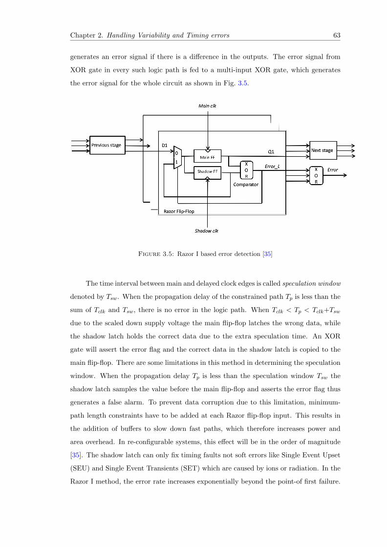
Chapter 2. Handling Variability and Timing errors 63
generates an error signal if there is a difference in the outputs. The error signal from
XOR gate in every such logic path is fed to a multi-input XOR gate, which generates
the error signal for the whole circuit as shown in Fig. 3.5.
Figure 3.5: Razor I based error detection [35]
The time interval between main and delayed clock edges is called speculation window
denoted by Tsw. When the propagation delay of the constrained path Tp is less than the
sum of Tclk and Tsw, there is no error in the logic path. When Tclk < Tp < Tclk+Tsw
due to the scaled down supply voltage the main flip-flop latches the wrong data, while
the shadow latch holds the correct data due to the extra speculation time. An XOR
gate will assert the error flag and the correct data in the shadow latch is copied to the
main flip-flop. There are some limitations in this method in determining the speculation
window. When the propagation delay Tp is less than the speculation window Tsw the
shadow latch samples the value before the main flip-flop and asserts the error flag thus
generates a false alarm. To prevent data corruption due to this limitation, minimum-
path length constraints have to be added at each Razor flip-flop input. This results in
the addition of buffers to slow down fast paths, which therefore increases power and
area overhead. In re-configurable systems, this effect will be in the order of magnitude
[35]. The shadow latch can only fix timing faults not soft errors like Single Event Upset
(SEU) and Single Event Transients (SET) which are caused by ions or radiation. In the
Razor I method, the error rate increases exponentially beyond the point-of first failure.

Chapter 2. Handling Variability and Timing errors 64
In [5], a similar approach to detect timing errors in FPGA-based circuits is pro-
posed. In this work, FPGA circuits are subjected to overclocking and the timing errors
in critical paths due overclocking are detected by shadow registers added to the critical
paths. The prime objective of this work is to monitor the effect of overclocking and
to decide how much overclocking can be applied with respect to the errors detected by
the shadow registers. This work outlines the scope of tolerating timing errors within a
margin to gain improvement in performance by overclocking. There is no scope for error
correction in this work.
3.3.1.2 Razor II
In order to avoid the above-mentioned limitations of Razor I, Razor II is proposed in
[37]. In Razor II, only error detection is performed using shadow flip-flops and the
error correction is performed using architecture replay (the last instruction is executed
again to obtain correct data). This makes the Razor II architecture simple and less area
consuming. But the architecture replay based error correction reduces the throughput
of the design. Razor II is also capable of detecting SER errors due to radiation. Fig. 3.6
shows the schematic of Razor II latch and its internal components like clock generator,
Transition Detector (TD) and Detection Clock (DC) generator. As shown in Fig. 3.7,
when the input data transitions occur after the rising edge of the clk, the shorter negative
pulse on DC suppresses the TD and the error flag is not asserted. However, during the
speculation window, if the input data transitions occur after the rising edge of the clk,
the TD detects the transition in the node N and results in assertion of the error signal
and instruction roll-back is carried out. The speculation windows of Razor II is from
the rising edge of the DC to falling edge of the clk. This can be extended at the cost
of more buffers to tackle the hold constraints. Razor II can also detect soft errors in
memory elements or propagated from logic to latch, as the TD is active during both the
phases of the clk. But when the DC is low, there is a chance that soft errors may not
be detected since the DC suppresses the TD.
Razor was designed for pipelined microprocessors, but it has never achieved com-
mercial success due to its overhead in fault correction in complex and high-frequency
instruction pipeline logic [5]. This is because the pipeline has to be stalled whenever
the error has to be corrected. All the existing error detection and correction methods
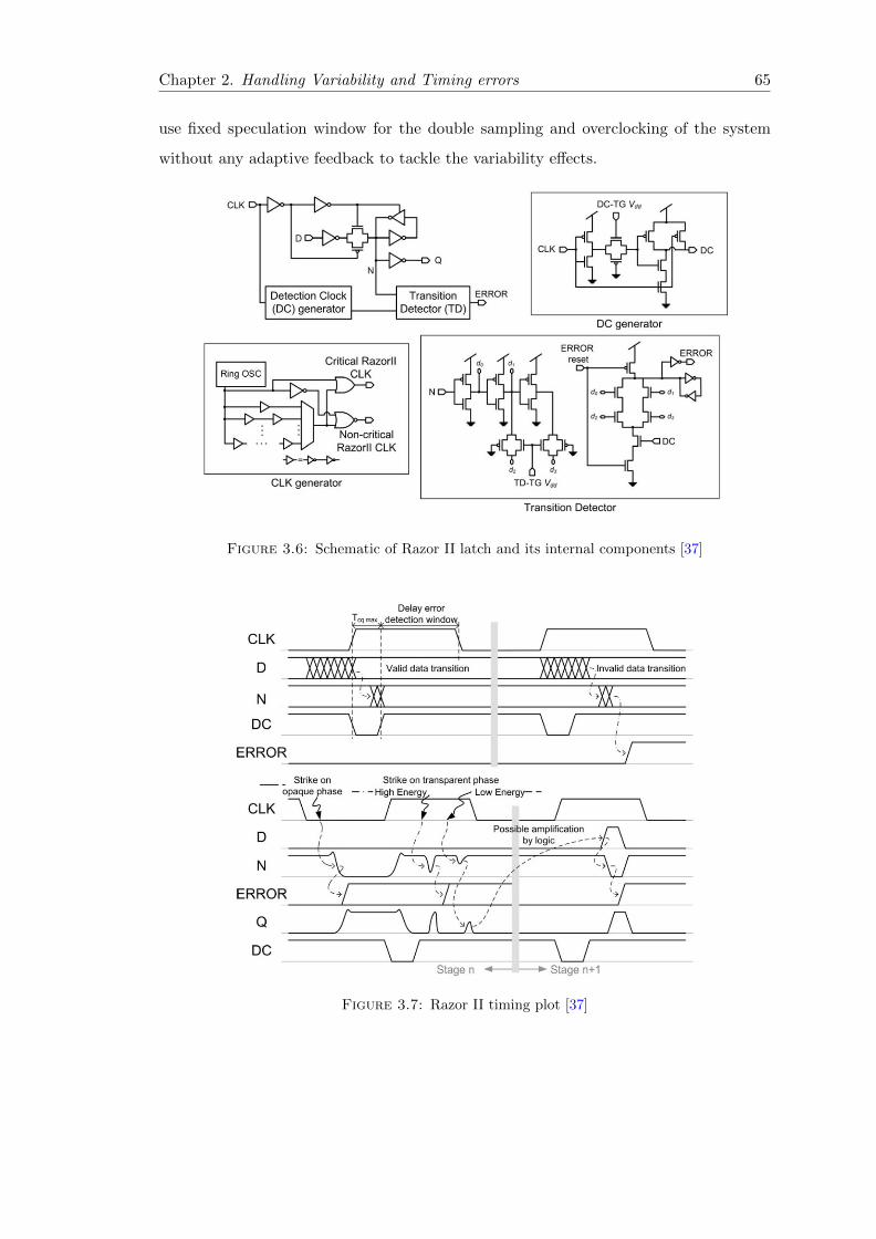
Chapter 2. Handling Variability and Timing errors 65
use fixed speculation window for the double sampling and overclocking of the system
without any adaptive feedback to tackle the variability effects.
Figure 3.6: Schematic of Razor II latch and its internal components [37]
Figure 3.7: Razor II timing plot [37]
Chapter 2. Handling Variability and Timing errors 66
3.3.2 Time Borrowing Methods
Time borrowing methods are another form of double sampling technique where latches
are used in place of registers. By taking the advantage of level triggering of latches,
timing error generated at one stage of the pipeline will be corrected by borrowing time
from the next stage of the pipeline. This type of local correction mechanism prevents
error from propagating across the pipeline.
3.3.2.1 Bubble Razor
As explained above, both the Razor methods have limitations due to timing issues.
They achieve high performance at the expense of long hold time which may lead to
race failure. Similarly, implementation of these methods is limited by architectural
invasiveness. In [38] an error detection technique based on two-phase latch timing and
local replay mechanism is proposed to overcome the limitations faced by both the Razor
methods. A conventional flip-flop based datapath can be converted into a two-phase
latch based datapath as shown in the Fig. 3.8. The logic delay in each phase is balanced
such that no time borrowing occurs during error-free operation. If the data arrives after
the latch opens due to variations or voltage scaling, Bubble Razor asserts error flag,
which guarantees that the error is caused by long paths taking more than a clock phase
instead of by short paths. With two-phase latches, when one latch is opening the latch
in the preceding stage is already closed. This feature of Bubble Razor provides more
speculation window and breaks the dependency of speculation window on short path
constraints unlike in Razor I and II. Bubble Razor uses time borrowing as a correction
mechanism by which architecture modifications and replaying instructions are avoided.
Because of its local correction mechanism, the function of the whole chip does not need to
be stalled. Fig. 3.9 shows the error detection and propagation of bubbles. A failure will
occur when data arrives after a latch closes, which can arise if the time borrowing effect
is not corrected and compounds through multiple stages. Upon detection of timing error,
error clock gating control signals called bubbles are propagated to neighboring latches.
A bubble causes a latch to skip its next transparent clock phase, giving it an additional
cycle for correct data to arrive. With two-phase latches, if a latch stalls, data is not
immediately lost because its neighboring latches operate out of phase. In order to not
lose data, neighboring latches must stall one clock phase later. Therefore half a clock

Chapter 2. Handling Variability and Timing errors 67
cycle to propagate bubble and another half a cycle to correct the error. To prevent the
bubbles from propagating indefinitely along loops, a bubble propagating algorithm is
proposed in [38]. 1) A latch that receives a bubble from one or more of its neighbors
stall and sends its other neighbors (input and output) a bubble half-cycle later; 2) A
latch that receives a bubble from all of its neighbors stall but does not send out any
bubbles as shown in Fig. 3.9. Multiple errors during the same cycle will cause multiple
bubble stalling sequences to take place at the same time, but when stall events collide,
they combine and are corrected in a single stall cycle, reducing correction overhead.
Figure 3.8: Schematic of Bubble Razor method [38]
3.3.3 GRAAL
Global Reliability Architecture Approach for Logic (GRAAL) is a latch based error
detection method used for pipelined architectures [39]. Compared to Razor methods and
other double sampling error detection methods where there is a penalty in duplicating
hardware or execution, GRAAL compares the result of a single computation observed
at two different instants. In this method, the logic constrained between flip-flops of
the pipelined architecture is partitioned into two equal slices and the slave latch of the
flip-flop is moved within the combinational logic by retiming. Two latches (masters
and slave) in every flip-flop of the conventional pipeline architecture clocked by non-
overlapping clocks φ1 and φ2 as shown in Fig. 3.10 . Thus, when one slice is computing,

Chapter 2. Handling Variability and Timing errors 68
Figure 3.9: Bubble Razor timing plot [38]
the adjacent stage is idle and its outputs are stable, enabling checking for temporary-
faults. This is not possible in flip-flop based design where the computations happen
simultaneously. An efficient tool is required to partition the combination logic into two
slices, such that the critical path of both the slices are equal and their sum is equal to
the delay of the un-partitioned combinational logic. For maximizing the fault tolerance
efficiency, clocks φ1 and φ2 have significant non-overlapping period such that each stage
will maintain stable values. In [39], duty cycle of φ1 and φ2 are 25% leaving another 25%
of non-overlapping period between them. The frequency of the clock has to be designed
in a way such that the falling edge of the clock φ1 occurs after the output from the
combination circuit is stable and the delay is denoted as D as shown in Fig. 3.11, where
δ is the minimum delay of the block. Therefore it is possible to compare the output
of combinational blocks CC1 and CC3 against the outputs of the respective latches L1
and L3 until the time period equal to 0.25T +δ, which is from the falling edge of φ1 to δ
time after the raising edge of φ2. There is no extra shadow latch required to detect the
error, also the speculation window is much wider compared to Razor methods, which
results in improved fault tolerance efficiency. In order to correct the errors, as shown in
Fig. 3.11, redundant flip-flops and MUXs are used like in Razor methods to memorize
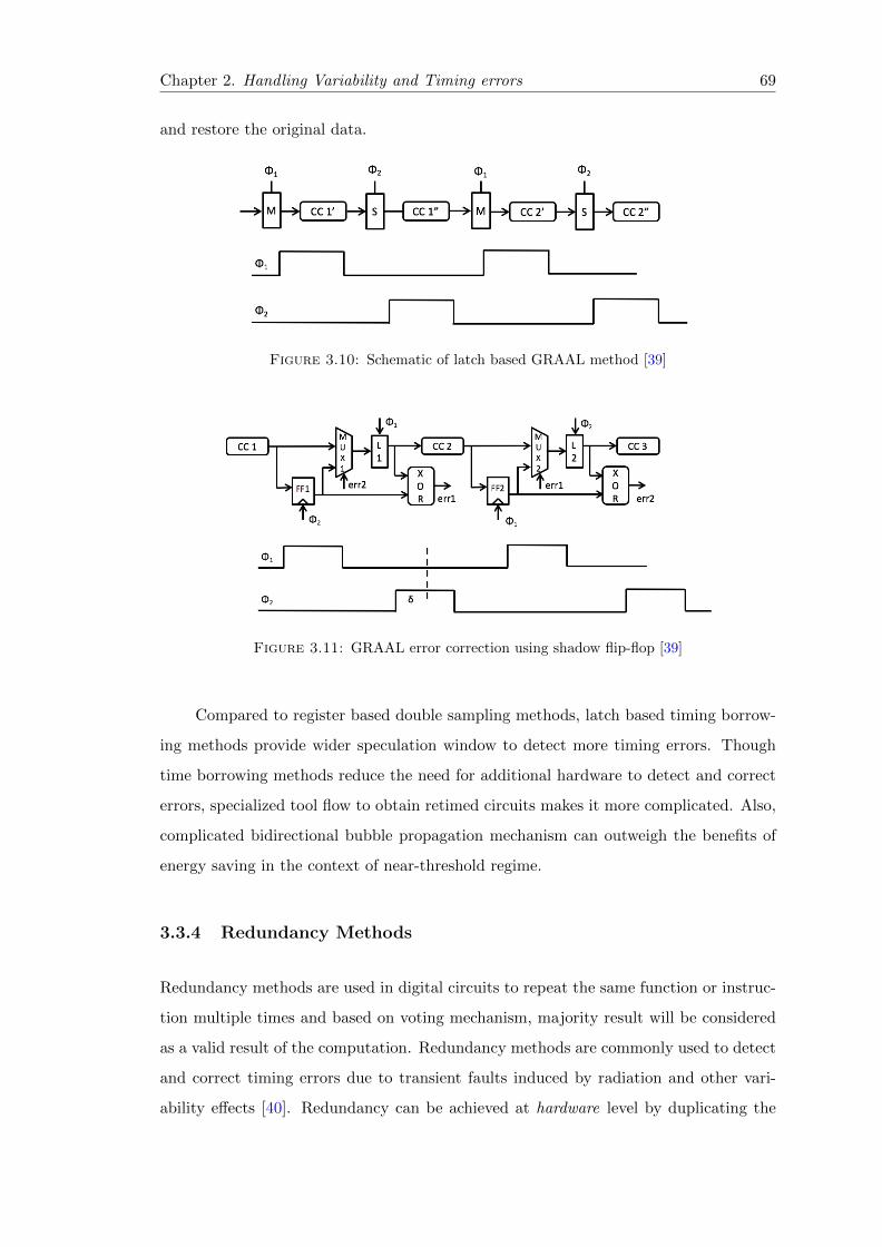
Chapter 2. Handling Variability and Timing errors 69
and restore the original data.
Figure 3.10: Schematic of latch based GRAAL method [39]
Figure 3.11: GRAAL error correction using shadow flip-flop [39]
Compared to register based double sampling methods, latch based timing borrow-
ing methods provide wider speculation window to detect more timing errors. Though
time borrowing methods reduce the need for additional hardware to detect and correct
errors, specialized tool flow to obtain retimed circuits makes it more complicated. Also,
complicated bidirectional bubble propagation mechanism can outweigh the benefits of
energy saving in the context of near-threshold regime.
3.3.4 Redundancy Methods
Redundancy methods are used in digital circuits to repeat the same function or instruc-
tion multiple times and based on voting mechanism, majority result will be considered
as a valid result of the computation. Redundancy methods are commonly used to detect
and correct timing errors due to transient faults induced by radiation and other vari-
ability effects [40]. Redundancy can be achieved at hardware level by duplicating the

Chapter 2. Handling Variability and Timing errors 70
functionality by additional hardware to execute same instruction multiple times in par-
allel or at software level by repeating the same instruction multiple times in the same
hardware. The software level redundancy is also called time redundancy. Unlike the
above-discussed Razor methods, where the pipeline registers/latches are duplicated to
achieve tolerance towards timing errors, in hardware redundancy, entire processing ele-
ments (PE) are duplicated. Since the context of this thesis is limited to hardware-based
methods, in the below sub-sections common hardware-based redundancy methods for
error detection and correction are discussed.
3.3.4.1 Flexible Error Handling Module (FEHM) based Triple Modular Re-
dundancy (TMR)
TMR is a hardware redundancy method, in which the functionality of a PE is duplicated
in two additional PEs. Based on voting mechanism the valid output is determined. This
type of hardware redundancy methods are most suitable for reconfigurable platform,
due to the availability of unused hardware to achieve redundancy [41]. In [42] a low cost
TMR for reconfigurable platform is proposed. In this method, Functional Units (FU) of
neighbouring PEs are clubbed together to execute an instruction. Output of these FUs
are passed to FEHM to determine the valid result as shown in Fig. 3.12.
Figure 3.12: TMR based on FEHM [42]
Fig. 3.13 shows the schematic of Flexible Error Handling Module. In the Data
error detection unit, outputs of all the channels are compared and error signal is sent
to Transition error detection unit and Voter mechanism. Voter mechanism selects the
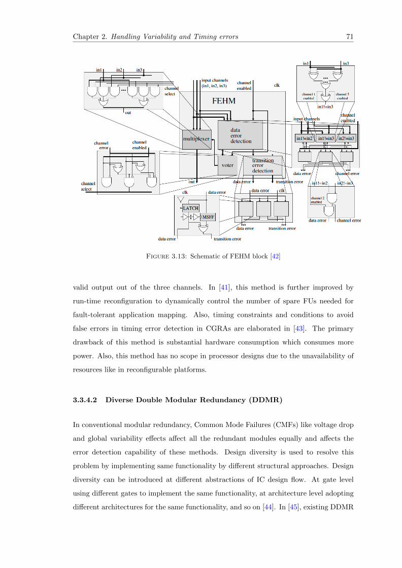
Chapter 2. Handling Variability and Timing errors 71
Figure 3.13: Schematic of FEHM block [42]
valid output out of the three channels. In [41], this method is further improved by
run-time reconfiguration to dynamically control the number of spare FUs needed for
fault-tolerant application mapping. Also, timing constraints and conditions to avoid
false errors in timing error detection in CGRAs are elaborated in [43]. The primary
drawback of this method is substantial hardware consumption which consumes more
power. Also, this method has no scope in processor designs due to the unavailability of
resources like in reconfigurable platforms.
3.3.4.2 Diverse Double Modular Redundancy (DDMR)
In conventional modular redundancy, Common Mode Failures (CMFs) like voltage drop
and global variability effects affect all the redundant modules equally and affects the
error detection capability of these methods. Design diversity is used to resolve this
problem by implementing same functionality by different structural approaches. Design
diversity can be introduced at different abstractions of IC design flow. At gate level
using different gates to implement the same functionality, at architecture level adopting
different architectures for the same functionality, and so on [44]. In [45], existing DDMR
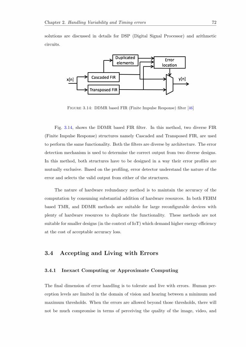
Chapter 2. Handling Variability and Timing errors 72
solutions are discussed in details for DSP (Digital Signal Processor) and arithmetic
circuits.
Figure 3.14: DDMR based FIR (Finite Impulse Response) filter [46]
Fig. 3.14, shows the DDMR based FIR filter. In this method, two diverse FIR
(Finite Impulse Response) structures namely Cascaded and Transposed FIR, are used
to perform the same functionality. Both the filters are diverse by architecture. The error
detection mechanism is used to determine the correct output from two diverse designs.
In this method, both structures have to be designed in a way their error profiles are
mutually exclusive. Based on the profiling, error detector understand the nature of the
error and selects the valid output from either of the structures.
The nature of hardware redundancy method is to maintain the accuracy of the
computation by consuming substantial addition of hardware resources. In both FEHM
based TMR, and DDMR methods are suitable for large reconfigurable devices with
plenty of hardware resources to duplicate the functionality. These methods are not
suitable for smaller designs (in the context of IoT) which demand higher energy efficiency
at the cost of acceptable accuracy loss.
3.4 Accepting and Living with Errors
3.4.1 Inexact Computing or Approximate Computing
The final dimension of error handling is to tolerate and live with errors. Human per-
ception levels are limited in the domain of vision and hearing between a minimum and
maximum thresholds. When the errors are allowed beyond those thresholds, there will
not be much compromise in terms of perceiving the quality of the image, video, and
Chapter 2. Handling Variability and Timing errors 73
audio. Therefore limitation in human perception level can be used to allow errors in the
computation or to design inexact hardware to perform approximate computing. This
provides two advantages: 1) no need for additional hardware to detect and correct er-
rors, and 2) energy and power savings can be achieved by trading the performance
and accuracy. Approximate computing can be achieved by inexact hardware and/or by
probabilistic approach in software and architecture. In [47], probabilistic approach in
the context of device modelling and circuit design is discussed in detail. A probabilistic
CMOS inverter can be described as erroneous with a probability p and correct with
a probability 1-p. In contrast to the deterministic CMOS inverter, the probabilistic
inverter exhibits wrong switching with respect to the probability of error p, where p
denotes the impact of all variability issues. A statistical model of the device is created
by knowing p. The probability of failure p is determined by varying Vdd, noise sources
and other device parameters. In [47], a 32-bit Conditional Carry Select (CCS) adder is
constructed with different Vdd for MSBs and LSBs to reduce power consumption. For
a pixel error in an HD Frame (1280 x 720) video streaming, 40% power reduction is
claimed.
Pruning based approximation in real-time video processing is proposed in [48].
Computation complexity of a direct Cholesky-decomposition-based solver in real-time
is very demanding. Based on observation, many elements in the decomposition can be
pruned with reduced accuracy is proposed. This results in 75% reduction in the number
of operations per solve, yielding benefits in terms of energy, computation time, and area.
In [49], a brief review of recent developments in approximate computing at different
abstractions from programming language to transistor level are discussed. Usability and
feasibility of approximate computing is determined by error metrics. Different error
metrics to determine the impact of approximate computing are also described in [49].
Approximations based on pruning methods are more rigid due to the removal of
some hardware to reduce the energy cost. This method lacks the dynamicity to switch
between different energy-accuracy trade-off points. On the other hand, methods based
on multiple voltage Vdd offer a better trade-off between energy efficiency and accuracy
but needs additional hardware like level-shifters to bridge the modules with different
supply voltage.

Chapter 2. Handling Variability and Timing errors 74
3.4.2 Lazy Pipelines
In [50], approximate computing technique based on Voltage Over-Scaling (VOS) is pro-
posed to improve the power efficiency and reduce error rate by utilizing vacant cycles in
VOS functional units. Based on voltage over-scaling and exploiting unutilized execution
cycles of FUs, Lazy Pipeline architecture is proposed. In this architecture, every FU
(precise FU ) in the pipeline is accompanied by an another FU (imprecise FU ) that is
operated at lower Vdd. Based on the required accuracy level definition in the instructions,
computations can be either performed by precise or imprecise FU. Set of FUs for each
precision level is recommended instead of scaling Vdd of a single FU. For an application
with n different precision levels a set of n FUs, each computing at a specific precision, is
needed. This increases the hardware consumption and complexity of the design. Based
on profiling of vacant cycles (slack), FU with reduced Vdd that can match the available
slack is used to compute the instruction.
In addition to hardware complexity, ISA (Instruction Set Architecture) of the ar-
chitecture also needs to be extended with precision marking for instructions to choose an
FU out of the set of FUs with different precision levels. The set of potential instructions
that can be subjected to approximate computing has to be determined offline. This
reduces the scope of dynamicity and quick adaptation to architectural changes.
3.5 Conclusion
In this chapter important insights about various error detection and correction methods
are provided. The chapter starts with an introduction to timing errors and taxonomy of
timing error tolerance at different levels of abstractions. Three major classifications of
error handling techniques are presented namely, 1) Predict and Prevent, 2) Detect and
Correct, and 3) Accept and Live. Predict and Prevent methods are suitable for designs
with longer sleep time and more relaxed area and power constraints. This limits the use
of these methods for design with ultra-low power techniques like DVS. Different detect
and correct techniques based on double sampling and timing borrowing are explained
in detail. The major limitations of the double sampling methods are fixed speculation
window, need for additional hardware like buffers, transition detectors etc., and complex
error correction methods like generation and propagation of bubbles. Likewise, time

Chapter 2. Handling Variability and Timing errors 75
borrowing method needs specialized tool flow to retime the design. Redundancy methods
like TMR and DDMR are only suitable for reconfigurable architecture with plenty of
unused resources. Finally, this chapter discusses the scope for accepting and living
with errors. Applications based on probabilistic computing can tolerate some margin
of error without compromising much of the output quality. Methods like pruning based
approximation, inexact computing with multiple Vdd are discussed and their limitations
are highlighted. Therefore, there is a need for a unified approach to handle errors based
on the application and end-user need. The required method should be able to detect
and correct errors at the same time, must give-up some margin of accuracy to gain more
in terms of energy based on user preference. Finally, the method should accommodate
different ultra-low power techniques like DVS, and Near-Threshold Computing to achieve
enhanced energy gains. In the rest of the thesis, we propose methods and frameworks
to meet these requirements and to overcome the mentioned limitations of the existing
methods.

Chapter 4
Dynamic Speculation Window
based Error Detection and
Correction
4.1 Introduction
Dynamic voltage and frequency scaling became the prominent way to reduce the energy
consumption in digital systems by trading the performance of the system to an acceptable
margin. Effect of scaling coupled with variability issues make highly pipelined systems
more vulnerable to timing errors [3]. Such errors have to be corrected at the cost of
additional hardware for proper functioning [4]. In Chapter 3, different error handling
methods are discussed in detail. The Razor method proposed in [35] is a very popular
error detection and correction architecture for timing errors in digital systems, inspired
by the more general double-sampling technique [4]. In the double-sampling architecture,
an additional sampling element, known as shadow register, is used along with the main
output register to sample the output at different timing instances. The shadow registers
are clocked by a delayed version of the main clock known as the shadow clock. The
timing interval between the rising edges of the main clock and the shadow clock is
termed as the speculation window (φ). The speculation window is used to compare the
main and shadow registers to determine the validity of the output.
77

Chapter 3. Dynamic Speculation based Error Detection and Correction 78
There is a trade-off between the width of the speculation window and the fault
coverage. For a wider speculation window, more errors could be detected and corrected,
but this requires more buffer insertion for logic paths that are shorter than the specu-
lation window to avoid false error detection. And vice-versa for a narrower speculation
windows. Designs with fixed speculation window optimized for certain operating condi-
tion might suffer from an increased error rate under variability issues such as thermal
effects. In order to tackle these limitations, a double-sampling technique with dynamic
speculation window is required to dynamically vary the speculation window with respect
to the variability effects.
Razor methods are not suitable for pipelined microprocessors due to its overhead
in fault correction in complex and high-frequency instruction pipeline logic [5]. Razor-
like fault detection and correction techniques are used in reconfigurable architectures
like Field-Programmable Gate Arrays (FPGA) and Coarse-Grain Reconfigurable Arrays
(CGRAs) due to moderate clock frequencies and function-specific pipelines [5], [6]. All
the existing error detection and correction methods use fixed speculation window for
the double sampling and overclocking of the system without any adaptive feedback to
tackle the variability effects.
In the rest of the chapter, the impact of overclocking and different double sampling
based error detection and correction methods are discussed. Subsequently, the idea of
Dynamic Speculation architecture and its advantages are proposed. Further dynamic
speculation based adaptive overclocking is explained. Proof of concept of the proposed
adaptive overclocking is explained with FPGA implementation. Finally, results of the
proposed method are discussed and contrasted with existing error detection and correc-
tion in the context of DVFS.
4.2 Overclocking and Error Detection in FPGAs
4.2.1 Impact of Overclocking in FPGAs
In general, FPGA designs can be safely overclocked by a significant ratio with respect to
the maximum operating frequency estimated by the FPGA’s synthesis and place-and-
route tool flow. This gives the advantage of increasing the implementation throughput

Chapter 3. Dynamic Speculation based Error Detection and Correction 79
without any design-level modifications. As a motivating example, an 8-bit 8-tap FIR
digital filter is synthesized and implemented in the Xilinx Virtex VC707 evaluation
board as shown in Fig. 4.1. The maximum operating clock frequency estimated by
Vivado 2014.4 tool flow, with performance optimized synthesis, is 167 MHz. A test
bench is created with an 80-bit LFSR, feeding random input patterns to the design,
and the output of the design is monitored using Vivado’s Integrated Logic Analyzer
(ILA). A functional simulation output obtained from RTL simulation is used to compare
the output of the ILA. Onboard IIC programmable LVDS (Low-Voltage Differential
Signaling) oscillator is used to provide clock frequency for the pattern generator and the
design under test. The supply voltage of the FPGA is not changed in this experiment.
XADC system monitor is used to record core voltage and temperature of the FPGA. At
the ambient temperature, the clock frequency is increased from 160 MHz to 380 MHz
and the output data is recorded for all the frequency steps.
Figure 4.1: Schematic of FIR filter overclocking in Virtex FPGA
Figure 4.2: Timing errors (percentage of failing critical paths and output bit errorrate) vs. Overclocking in FPGA configured with an 8-bit 8-tap FIR filter
Chapter 3. Dynamic Speculation based Error Detection and Correction 80
Fig. 4.2 shows the evolution of Bit Error Rate (ratio of faulty bits over total output
bits) at the output of the design with respect to overclocking. In Fig. 4.2, the first plot
(orange squares) represents the percentage of critical paths that fail when the FPGA
is overclocked. Similarly, the second curve (blue diamonds) represents the output BER
(Bit Error Rate). As shown in Fig. 4.2, there are no errors recorded until 260MHz,
which gives the safe overclocking margin of 55% with respect to the maximum operating
frequency estimated by Vivado, and therefore a performance gain of 1.55×. Beyond
this safe overclocking margin, some critical paths in the design start to fail and the
output error rate increases exponentially with respect to the increase in the clock fre-
quency. Overclocking up to 300 MHz (×1.8 the operating frequency) leads to BER of
10%, which would be still acceptable for applications that tolerate approximate compu-
tations [51]. Around 350 MHz, all critical paths fail and the bit error rate converges to
50%. By employing error detection and correction mechanisms such as double-sampling
methods, FPGA designs can be adaptively overclocked to improve performance at run
time according to varying operating conditions (e.g., temperature).
4.2.2 Double Sampling
Error detection based on the double-sampling scheme requires less area and power over-
head than traditional concurrent detection methods such as Double Modular Redun-
dancy (DMR) [4]. In the double-sampling method, instead of replicating the entire
pipeline, an additional sampling element (latch or flip-flop) is added at the output of
the pipeline to sample the output data at two different time instances using the main
clock (Mclk) and a shadow clock (Sclk). In Fig. 4.3, a logic path Path1 is constrained
between the input register R1 and the output register Q1. An additional shadow register
S1 also samples the output data at different timing instance. An XOR gate is used to
compare the data from the registers Q1 and S1. An error register E1 is used to record
any discrepancies between output data from Q1 and S1. The multiplexer M1 is used to
select the valid output for error correction based on error signal from the register E1.
In [52], instead of using a delayed shadow clock, the delay is added to the combinational
logic output to prevent the variation due to aging effects. Different versions of double-
sampling methods are proposed in [52]. Razor I [35], Razor II [37], Bubble Razor [38],
GRAAL [39] are commonly used in digital designs for detecting timing errors and coun-
teracting the effect of dynamic voltage and frequency scaling (DVFS). Bubble Razor [38]
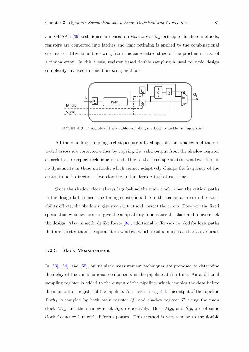
Chapter 3. Dynamic Speculation based Error Detection and Correction 81
and GRAAL [39] techniques are based on time borrowing principle. In these methods,
registers are converted into latches and logic retiming is applied to the combinational
circuits to utilize time borrowing from the consecutive stage of the pipeline in case of
a timing error. In this thesis, register based double sampling is used to avoid design
complexity involved in time borrowing methods.
Figure 4.3: Principle of the double-sampling method to tackle timing errors
All the doubling sampling techniques use a fixed speculation window and the de-
tected errors are corrected either by copying the valid output from the shadow register
or architecture replay technique is used. Due to the fixed speculation window, there is
no dynamicity in these methods, which cannot adaptively change the frequency of the
design in both directions (overclocking and underclocking) at run time.
Since the shadow clock always lags behind the main clock, when the critical paths
in the design fail to meet the timing constraints due to the temperature or other vari-
ability effects, the shadow register can detect and correct the errors. However, the fixed
speculation window does not give the adaptability to measure the slack and to overclock
the design. Also, in methods like Razor [35], additional buffers are needed for logic paths
that are shorter than the speculation window, which results in increased area overhead.
4.2.3 Slack Measurement
In [53], [54], and [55], online slack measurement techniques are proposed to determine
the delay of the combinational components in the pipeline at run time. An additional
sampling register is added to the output of the pipeline, which samples the data before
the main output register of the pipeline. As shown in Fig. 4.4, the output of the pipeline
Path1 is sampled by both main register Q1 and shadow register T1 using the main
clock Mclk and the shadow clock Sclk respectively. Both Mclk and Sclk are of same
clock frequency but with different phases. This method is very similar to the double

Chapter 3. Dynamic Speculation based Error Detection and Correction 82
sampling technique discussed in the previous subsection. The only difference is that the
shadow clock Sclk always leads the main clock Mclk by a phase difference φ. An XOR
gate is used to compare the outputs from both main register Q1 and shadow register
T1. The output of the XOR gate is sampled by error register e1. To determine the
available positive slack of the pipeline Path1, the phase difference φ is increased until
the error register e1 records an error. Due to the leading shadow clock, this method is
not capable of detecting timing errors in the critical paths that violate timing constraints
due to temperature or other variability effects.
Figure 4.4: Principle of online slack measurement for overclocking
4.3 Proposed Method for Adaptive Overclocking
In this thesis, dynamic speculation window combined with the double-sampling method
is proposed for error detection and correction and to adaptively overclock or underclock
the design based on variability effects. The following sections present the proposed
architecture of a dynamic speculation window and the adaptive feedback loop for over-
/under-clocking the design.
4.3.1 Dynamic Speculation Window Architecture
Fig. 4.5, shows the schematic of the proposed dynamic speculation window architecture.
In a pipelined digital design, logic paths are time constrained between input and output
registers. Fig. 4.5 shows a design with n logic paths Pathi constrained between input
and output registers Ri and Qi respectively. In the rest of this section, let us consider one
path Path1 out of n logic paths for easy understanding. As shown in Fig. 4.5, logic path
Path1 is constrained between input register R1 and output register Q1. Two shadow
registers S1 and T1 are added to sample the output of the Path1, in contrast to the one

Chapter 3. Dynamic Speculation based Error Detection and Correction 83
shadow register approach in [5], [6], and [7]. T1 is used to measure the available slack
in the path which can be used to overclock the design. While S1 is used to sample the
valid data when the delay of the Path1 is not meeting the timing constraints of the main
clock M clk due to the variability effects. Similar to double-sampling architectures, it
is assumed that the shadow register S1 always samples the valid data. In this setup,
all three registers S1, Q1 and T1 use the same clock frequency but different phases to
sample the output. The main output register Q1 samples the output at the rising edge of
M clk, while shadow register S1 samples the output at the falling edge of M clk. Shadow
register T1 samples the output at the rising edge of the shadow clock S clk generated by
the phase generator. Two XOR gates compare the data in main and shadow registers
S1 and T1, the corresponding error values are registered in E1 and e1. The registers E1
and e1 are clocked by falling and rising edge of the M clk respectively.
Figure 4.5: Principle of the dynamic speculation window based double-samplingmethod. Solid lines represent data and control between modules, dashed lines repre-sent main clock, dash-dot-dash lines represent shadow clock, and dotted lines represent
feedback control
Fig. 4.6 shows the timing diagram of the proposed method. In Fig. 4.6a, the
shadow clock (S clk) leads the main clock (M clk) by phase φ1. Since the Data (output
of Path1) is available before the rising edge of the shadow clock, the valid data is sampled
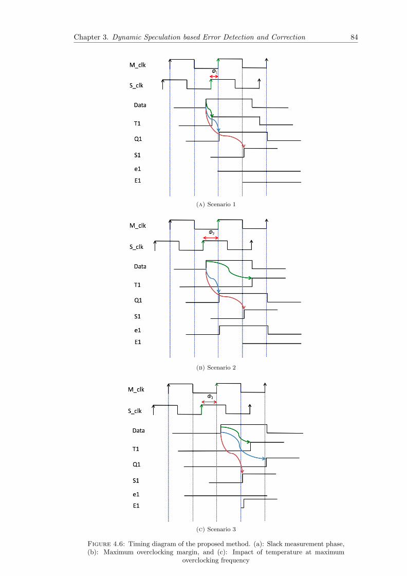
Chapter 3. Dynamic Speculation based Error Detection and Correction 84
(a) Scenario 1
(b) Scenario 2
(c) Scenario 3
Figure 4.6: Timing diagram of the proposed method. (a): Slack measurement phase,(b): Maximum overclocking margin, and (c): Impact of temperature at maximum
overclocking frequency
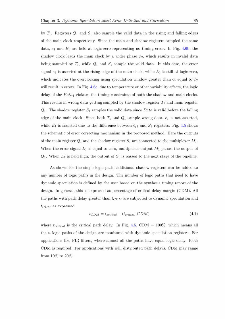
Chapter 3. Dynamic Speculation based Error Detection and Correction 85
by T1. Registers Q1 and S1 also sample the valid data in the rising and falling edges
of the main clock respectively. Since the main and shadow registers sampled the same
data, e1 and E1 are held at logic zero representing no timing error. In Fig. 4.6b, the
shadow clock leads the main clock by a wider phase φ2, which results in invalid data
being sampled by T1, while Q1 and S1 sample the valid data. In this case, the error
signal e1 is asserted at the rising edge of the main clock, while E1 is still at logic zero,
which indicates the overclocking using speculation window greater than or equal to φ2
will result in errors. In Fig. 4.6c, due to temperature or other variability effects, the logic
delay of the Path1 violates the timing constraints of both the shadow and main clocks.
This results in wrong data getting sampled by the shadow register T1 and main register
Q1. The shadow register S1 samples the valid data since Data is valid before the falling
edge of the main clock. Since both T1 and Q1 sample wrong data, e1 is not asserted,
while E1 is asserted due to the difference between Q1 and S1 registers. Fig. 4.5 shows
the schematic of error correcting mechanism in the proposed method. Here the outputs
of the main register Q1 and the shadow register S1 are connected to the multiplexer M1.
When the error signal E1 is equal to zero, multiplexer output M1 passes the output of
Q1. When E1 is held high, the output of S1 is passed to the next stage of the pipeline.
As shown for the single logic path, additional shadow registers can be added to
any number of logic paths in the design. The number of logic paths that need to have
dynamic speculation is defined by the user based on the synthesis timing report of the
design. In general, this is expressed as percentage of critical delay margin (CDM). All
the paths with path delay greater than tCDM are subjected to dynamic speculation and
tCDM as expressed
tCDM = tcritical − (tcritical.CDM) (4.1)
where tcritical is the critical path delay. In Fig. 4.5, CDM = 100%, which means all
the n logic paths of the design are monitored with dynamic speculation registers. For
applications like FIR filters, where almost all the paths have equal logic delay, 100%
CDM is required. For applications with well distributed path delays, CDM may range
from 10% to 20%.

Chapter 3. Dynamic Speculation based Error Detection and Correction 86
4.3.2 Adaptive Over-/Under-clocking Feedback Loop
Fig. 4.5 shows the feedback loop of the proposed method. The error signals Ei and
ei from all the monitored paths are connected to Error Counter and Slack Counter
respectively. For different speculation windows φi, Error Counter and Slack Counter
count the discrepancies in the paths being monitored.
• The Slack Counter denotes the number of timing errors due to overclocking or
voltage overscaling the design.
• The Error Counter denotes the number of timing errors due to variability effects.
For a design, clocked at the maximum clock frequency, considering no variability
effects, both Error Counter and Slack Counter will be zero. This indicates no tim-
ing errors in the design. To increase the performance, the design can be subjected to
overclocking. Phase Generator in the feedback loop is used to generate different phases
of the shadow clock S clk which is used to determine the maximum safe overclocking
margin (overclocking with out timing errors) by measuring the available slack. In the
proposed setup, a dedicated register is used to measure the available slack in the design.
This isolates the functioning of the pipeline from slack measuring process. When the
phase difference φ between M clk and S clk increases, critical paths in the design tends
to fail to indicate the limit of maximum safe overclocking margin. Slack register Ti first
detects those timing errors and increment the Slack Counter with respect to the num-
ber of failing paths. In this case, Error Counter will be still zero since the functioning
of the pipeline is not disturbed. Based on the Slack Counter value, overclocking or
voltage overscaling is controlled in the feedback loop.
Certain error resilient applications can tolerate some amount of errors in the com-
putation. In the feedback loop, SC margin is the user-defined error tolerance margin
due to overclocking or voltage overscaling. For applications that can tolerate timing
errors, SC margin can be set to allow overclocking or voltage overscaling to improve the
performance or energy efficiency of the design respectively.
Under variability effects, some or most of the logic paths in the design will fail,
the value of the Error Counter is incremented with respect to the number of failing
paths. This triggers the error correction mechanism to pass valid data from shadow

Chapter 3. Dynamic Speculation based Error Detection and Correction 87
register Si to the next stage. Based on the Error Counter value, feedback loop decides
to lower the clock frequency or increase the supply voltage to reduce the timing errors.
As mentioned earlier, for error resilient applications, EC margin can be set to tolerate
acceptable error margin without lowering the clock frequency or increasing the supply
voltage.
Therefore, SC margin sets the limit for timing errors that can be tolerated in order
to increase the performance or energy efficiency of the design. Likewise, EC margin
sets the limit for timing errors due to variability effects that can be tolerated without
compromising the performance or energy efficiency. Both SC margin and EC margin
are defined as a percentage of CDM. For applications that demand high accuracy both
SC margin and EC margin are set to 0%. This forces the feedback loop to safely over-
clock (without any timing errors) the design and no tolerance towards timing errors due
to variability effects. The tolerable error margin of Error Counter and Slack Counter
are determined from the timing reports after synthesis and placement of the design.
4.4 Proof of Concept using Xilinx Virtex FPGA
The proposed Dynamic Speculation Window in the double-sampling method is imple-
mented in a Xilinx Virtex VC707 evaluation board as shown in Fig. 4.7. In this exper-
iment, we have demonstrated adaptive overclocking in Xilinx Virtex 7 FPGA based on
dynamic speculation method. This method can be further extended to voltage overscal-
ing in platforms that are compatible with voltage scaling. Vivado tool flow is used to
synthesize and implement the RTL benchmarks into the FPGA. A testbench is created
for all the benchmark designs with an 80-bit LFSR pattern generator for random in-
puts to the design under test. Onboard IIC programmable LVDS oscillator is used to
provide clock frequency for the pattern generator and the design under test. As shown
in Fig. 4.7, control signals from the Error Counter and the Slack Counter determine
the output frequency of the LVDS oscillator. Different phases of the generated clock
frequency are obtained from the inbuilt Mixed-Mode Clock Manager (MMCM) module
in the FPGA [56]. The core temperature is monitored through XADC system moni-
tor, and the temperature is varied by changing the RPM (rotations per minute) of the
cooling fan.

Chapter 3. Dynamic Speculation based Error Detection and Correction 88
Figure 4.7: Experimental setup of Adaptive overclocking based on Dynamic Specu-lation
For error-free overclocking, Slack Counter margin is set to zero. At the ambient
core temperature of around 28◦C, when Error Counter and Slack Counter are equal
to zero, the speculation window φ is increased for every clock cycle from 0◦ to 180◦ at
discrete intervals of 25◦ until the Slack Counter records an error. Beyond 180◦ up to
360◦, the speculation window width repeats due to periodic nature of the clock. Once
the slack counter records an error, the system is put on halt and safely overclocked
by trading the available slack. While the speculation window φ is swept, the pipeline
functions normally since the output register Qi and the shadow register Si sample the
same valid data. Regarding error correction due to variability effects, if Error Counter
records more than 2% of the monitored paths not meeting the timing constraints, the
system is put on halt and the operating frequency of the system is decreased in multiples
of a clock frequency step δ to reduce the errors (in our test platform the frequency step
is δ = 5MHz). Since correcting more errors will reduce the throughput of the design,
decreasing the operating frequency is a necessary measure. Multiplexer Mi, as shown
in Fig. 4.5, corrects the error by connecting the output of the shadow register Si to the
next stage of the pipeline. Once the temperature falls back, the operating frequency of
the design is again increased based on the slack measurement as described earlier.
To highlight the adaptive overclocking and timing error detection and correction
capability of the proposed method, we have implemented a set of benchmark designs
in both Razor-based method [5] and the proposed dynamic speculation window based
Chapter 3. Dynamic Speculation based Error Detection and Correction 89
method. Benchmarks used in this experiments are common datapath elements like
FIR filter (8 taps, 8 bits), and various versions of 32-bit adder and 32-bit multiplier
architectures. After implementation, timing reports are generated to spot the critical
paths in the design. Timing and location constraints are used to place the shadow
registers Si and Ti close to the main output register Qi for all the output bits of the
design. For the Razor-based method, all the monitored paths are annexed with one
shadow register Si in contrast to the proposed method with two shadow registers, and
the logic paths that are shorter than speculation window are automatically annexed with
buffers by the synthesis tool. For comparison purpose, both the Razor-based method
and the proposed method are subjected to identical test setup. In both cases, the design
is overclocked beyond the maximum frequency estimated by Vivado and the FPGA’s
core temperature is varied to introduce variability effects in the design.
After the synthesized bitstream is programmed into the FPGA and the design is
initially clocked at the maximum frequency (Fmax) estimated by Vivado for each design.
At the ambient core temperature of around 28◦C, the speculation window φ is increased
for every clock cycle and if the Slack Counter is zero at the widest speculation window,
then the clock frequency can be increased up to 40% because at 180◦, φ corresponds to
half of the clock period. That implies all the critical paths in the design have positive
slack equals to half of the clock period. Overclocking is done by halting the design
and increasing the clock frequency from the LVDS oscillator. The LVDS oscillator is
programmed through the IIC bus with the pre-loaded command word for the required
frequency. After changing the frequency, again the phase sweep starts from 0◦ until the
Slack Counter records an error. This way, the error-free overclocking margin of each
design is determined with respect to the maximum operating frequency estimated by
Vivado.
While operating at the safe overclocking Fmax at 28◦C, the core temperature of
the FPGA is varied by changing the RPM of the cooling fan. Due to the increase in
temperature, the critical paths of the design starts to fail. When the Error Counter
records an error in more than 2% of the monitored paths, the design is put on halt
and the frequency is reduced in multiples of 5MHz until the Error Counter margin is
below 2%. Since the shadow register Si latches the correct output, errors are corrected
without re-executing for that particular input pattern. The tolerance margin is used to

Chapter 3. Dynamic Speculation based Error Detection and Correction 90
Table 4.1: Synthesis results of different benchmark designs
BenchmarksArea without Area overhead for Area overhead for
error detection Proposed method Razor methodLUTs FFs LUTs FFs LUTs FFs
8-tap 8-bit FIR Filter 1279 1547 2.5% 2% 2% 1%
Unsigned 32-bit Multiplier 7270 4511 1.9% 1.7% 2.3% 0.9%
Signed 32-bit Wallace Tree Multiplier 5997 4458 2.8% 1.8% 3.2% 1%
32-bit Kogge-Stone Adder 3944 4117 3.7% 1.7% 4% 1.2%
32-bit Brent-Kung Adder 3753 4053 3.3% 1.9% 3.8% 1%
Table 4.2: Estimated Fmax and safe overclocking Fmax of benchmark designs at 28◦C
BenchmarksEstimated
Safe Safe
Fmax (MHz)overclocking overclockingFmax at 28◦C margin
(in MHz) at 28◦C
8-tap 8-bit FIR Filter 167 260 55%
Unsigned 32-bit Multiplier 76 130 71%
Signed 32-bit Wallace Tree Multiplier 80 135 69%
32-bit Kogge-Stone Adder 130 215 64%
32-bit Brent-Kung Adder 135 216 60%
reduce the overhead in error correction mechanism which can affect the throughput of
the design.
Table 4.1 provides synthesis results of the benchmarks without any error detection
technique, with razor flip-flops [5], and with proposed error detection and correction
technique. The area overhead of the proposed method compared to the original design
is kept between 3.6% to 5.4%, which demonstrates the applicability of the technique in
real designs. Table 4.1 also provides the maximal frequency Fmax estimated by Vivado.
The Look-Up Table (LUT) overhead of the proposed method is on average 0.4% less
compared to the Razor implementation, since no buffers are needed for the shorter paths.
However, Flip-Flop (FF) overhead of the proposed method is 0.8% more compared to
the Razor method due to the two shadow flip-flops used for slack measurement and error
correction.
Table 4.2, shows the estimated Fmax of all the benchmark designs and the safe
overclocking Fmax that can be reached by the proposed error detection method at an
ambient temperature of 28◦C. As an example, for the FIR filter design, Vivado estimated
Fmax is 167MHz. However, this design can be overclocked at the ambient temperature
by more than 55% up to 260MHz, without any error, and up to 71% for the other
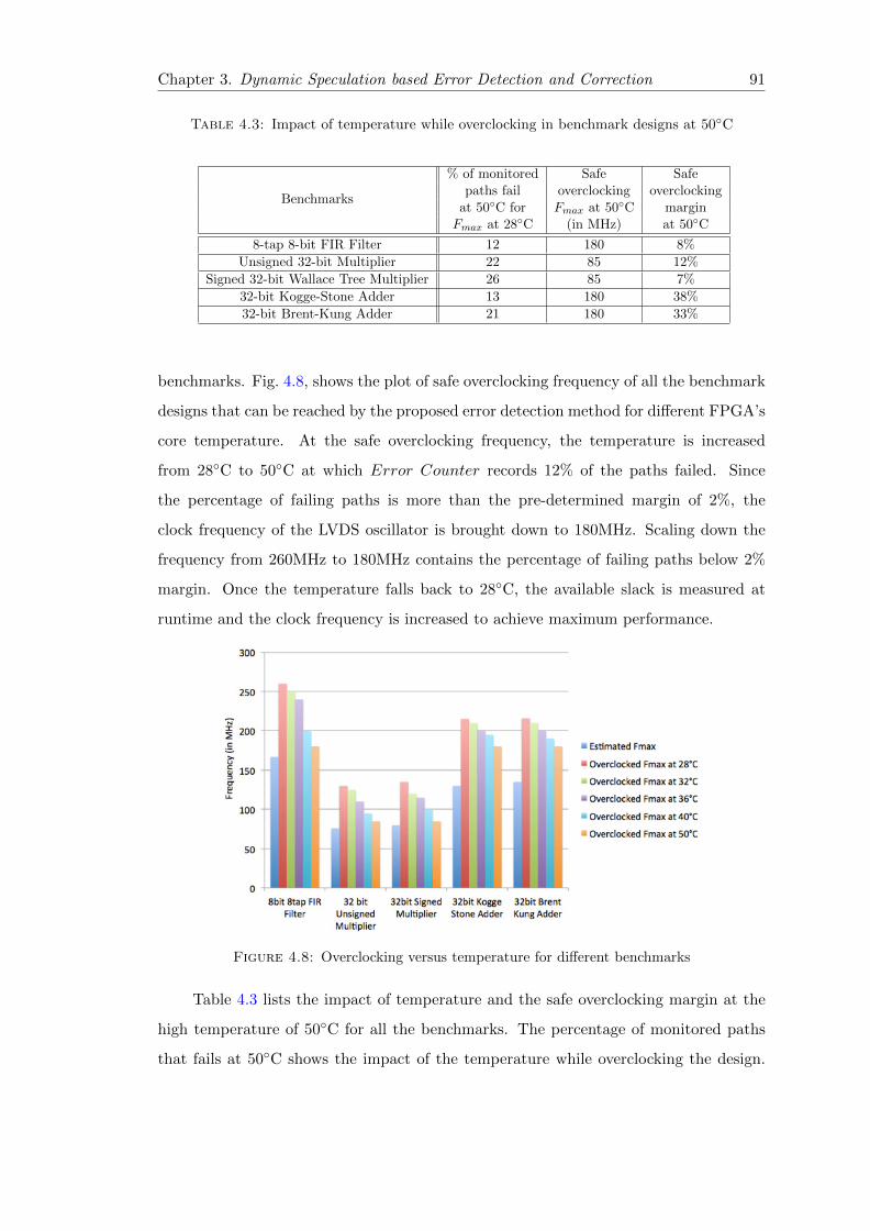
Chapter 3. Dynamic Speculation based Error Detection and Correction 91
Table 4.3: Impact of temperature while overclocking in benchmark designs at 50◦C
Benchmarks
% of monitored Safe Safepaths fail overclocking overclocking
at 50◦C for Fmax at 50◦C marginFmax at 28◦C (in MHz) at 50◦C
8-tap 8-bit FIR Filter 12 180 8%
Unsigned 32-bit Multiplier 22 85 12%
Signed 32-bit Wallace Tree Multiplier 26 85 7%
32-bit Kogge-Stone Adder 13 180 38%
32-bit Brent-Kung Adder 21 180 33%
benchmarks. Fig. 4.8, shows the plot of safe overclocking frequency of all the benchmark
designs that can be reached by the proposed error detection method for different FPGA’s
core temperature. At the safe overclocking frequency, the temperature is increased
from 28◦C to 50◦C at which Error Counter records 12% of the paths failed. Since
the percentage of failing paths is more than the pre-determined margin of 2%, the
clock frequency of the LVDS oscillator is brought down to 180MHz. Scaling down the
frequency from 260MHz to 180MHz contains the percentage of failing paths below 2%
margin. Once the temperature falls back to 28◦C, the available slack is measured at
runtime and the clock frequency is increased to achieve maximum performance.
Figure 4.8: Overclocking versus temperature for different benchmarks
Table 4.3 lists the impact of temperature and the safe overclocking margin at the
high temperature of 50◦C for all the benchmarks. The percentage of monitored paths
that fails at 50◦C shows the impact of the temperature while overclocking the design.

Chapter 3. Dynamic Speculation based Error Detection and Correction 92
The operating frequency has to be scaled down to limit these errors which can be even-
tually corrected by the error correction technique in the proposed method. Even at the
higher temperature of 50◦C, the FIR filter is safely overclocked up to 8% compared to
the maximum frequency estimated by Vivado. Similarly, at 50◦C, both unsigned and
signed multiplier architectures can be safely overclocked up to 12% and 7% respectively.
A maximum safe overclocking margin of 38% is achieved for the Kogge-Stone adder
and 33% by the Brent-Kung adder while operating at 50◦C. These results demonstrate
the adaptive overclocking, and error detection and correction capability of the proposed
method with a limited area overhead in the FPGA resources.
Figure 4.9: Comparison of Razor-based feedback look and the proposed dynamicspeculation window. Curve in blue diamond represents the FPGA’s core temperature.Curve in red square represents the frequency scaling by the proposed method. Green
triangle curve represents the frequency scaling by the Razor-based method
Fig. 4.9, shows the comparison of the proposed dynamic speculation window and
the Razor-based overclocking for the 8-bit 8-tap FIR filter design in Virtex 7 FPGA.
The core temperature of the FPGA is varied by controlling the speed of the cooling fan.
As shown in Fig. 4.9, the FPGA’s core temperature is increased from the ambient room
temperature of 28◦C to 50◦C and then decreased again back to the room temperature.
When the temperature increases, critical paths in the design starts to fail, which makes
the proposed method and the Razor-based method to scale down the frequency to limit
the error below 2% of monitored paths. Initially, at the room temperature, the design
is running at 260 MHz. At the temperature of 50◦C, the frequency is scaled down
to 180 MHz. When the temperature falls back to the room temperature, the proposed
method is able to measure the available slack in the pipeline and to increase the frequency
to overclock the design and therefore to increase performance. Under similar test setup,
Chapter 3. Dynamic Speculation based Error Detection and Correction 93
the Razor-based feedback loop scales down the frequency as the temperature increases.
However, when the temperature falls back, there is no change in the frequency. This
is because the Razor implementation does not have the slack measurement in place to
adaptively change the frequency when the temperature is reducing. Due to the additional
shadow register placed in the proposed method, the system is able to measure the slack
available in the pipeline which is traded to overclock the design according to temperature
fluctuations. This gives a more upper hand for the proposed dynamic speculation window
based error detection method over the classical Razor-based timing error detection.
4.5 Comparison with Related Works
4.5.1 DVFS with slack measurement
In [7], an online slack measurement technique based on [53], [54], and [55] is used to
scale the supply voltage or frequency to increase the energy savings. The output of the
path under monitoring (PUM) is sampled by both main register and shadow register
using same clock frequency but different phases as shown in Fig. 4.4.
Here the basic assumption is that the main register meets the timing constraints
in all situations, in other words, there is no scope for timing errors or error correction in
this method. The shadow register is clocked by different phases of the main clock. An
error register records errors by comparing output data from both the main and shadow
registers. The number of logic paths to be monitored by inserting a shadow register
is pre-determined (represented as a certain percentage of the Critical Delay Margin) in
contrast to [35]. This reduces the area cost by not appending shadow registers for all the
logic paths in the circuit. Also, the paths that are shorter than the speculation window
are not monitored, which voids the need for buffer insertion in shorter paths. When
the shadow clock leads the main clock by phase φ, if the PUM finished the execution
before the rising edge of the shadow clock, a valid output data is sampled by both the
shadow and main registers. The phase φ is further increased until the shadow register
records invalid data while main register samples the valid data. The measured slack is
compared with the pre-determined guardband to increase the energy savings by scaling
the voltage or frequency. This method is providing energy saving without any scope for
error detection or correction. Compared to the proposed dynamic speculation method,

Chapter 3. Dynamic Speculation based Error Detection and Correction 94
since the shadow clock is leading the main clock, it cannot detect the error when the
critical path violates the main clock timing constraints due to temperature and other
variability effects.
In [57],[58], an in-situ monitor (ISM) is proposed to identify timing errors due to
variability effects. In this method, three speculation windows are evaluated using three
delay chains and a multiplexer to detect the timing errors. Unlike the proposed dynamic
speculation method, this method can only detect timing errors but not provide any scope
for overclocking to achieve energy gains. In [58], the effect of temperature is studied to
demonstrate the robustness of the method, but the impact of dynamic temperature
variations and the adaptability of the ISM to overscale or underscale the frequency and
voltage is not well established.
4.5.2 Timing error handling in FPGA and CGRA
In [5], the advantages of using Razor-based error detection and correction in FPGA
implementations to increase energy efficiency are discussed. In this method, a timing
fault detector (TFD) is added to the pre-determined number of logic paths in the FPGA
implementation. The TFD block consists of a shadow register, an XOR gate, and a fault
register. Adding shadow registers is carried out by altering the netlist obtained during
the post-placement stage. Based on the timing report and the post-placement netlist,
unused resources in the FPGA are used for TFDs. Since the TFDs are placed after the
placement and routing of the main design, the delay between the output of the logic path
and the shadow register might not be same as the delay between the output of the logic
path and the main register. This difference in the delay between the main register and
the shadow register is compensated by adjusting the shadow clock lag. After placing the
TFDs, the FPGA is overclocked beyond the maximum frequency estimate given by the
FPGA timing tool under fixed temperature and supply voltage. The scope of this method
is only detecting the fault rate for different frequencies beyond the maximum frequency.
No error correction technique is proposed nor the variability issues are discussed.
In [6], overclocking CGRAs using Razor is presented. This method focuses on im-
plementing Razor in 2D arrays and propagating stall signals to correct the errors due
to overclocking. However, this method is also not discussing adaptively changing the
frequency based on temperature and variability effects. Similarly, [43] presents timing
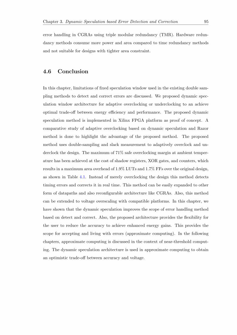
Chapter 3. Dynamic Speculation based Error Detection and Correction 95
error handling in CGRAs using triple modular redundancy (TMR). Hardware redun-
dancy methods consume more power and area compared to time redundancy methods
and not suitable for designs with tighter area constraint.
4.6 Conclusion
In this chapter, limitations of fixed speculation window used in the existing double sam-
pling methods to detect and correct errors are discussed. We proposed dynamic spec-
ulation window architecture for adaptive overclocking or underclocking to an achieve
optimal trade-off between energy efficiency and performance. The proposed dynamic
speculation method is implemented in Xilinx FPGA platform as proof of concept. A
comparative study of adaptive overclocking based on dynamic speculation and Razor
method is done to highlight the advantage of the proposed method. The proposed
method uses double-sampling and slack measurement to adaptively overclock and un-
derclock the design. The maximum of 71% safe overclocking margin at ambient temper-
ature has been achieved at the cost of shadow registers, XOR gates, and counters, which
results in a maximum area overhead of 1.9% LUTs and 1.7% FFs over the original design,
as shown in Table 4.1. Instead of merely overclocking the design this method detects
timing errors and corrects it in real time. This method can be easily expanded to other
form of datapaths and also reconfigurable architecture like CGRAs. Also, this method
can be extended to voltage overscaling with compatible platforms. In this chapter, we
have shown that the dynamic speculation improves the scope of error handling method
based on detect and correct. Also, the proposed architecture provides the flexibility for
the user to reduce the accuracy to achieve enhanced energy gains. This provides the
scope for accepting and living with errors (approximate computing). In the following
chapters, approximate computing is discussed in the context of near-threshold comput-
ing. The dynamic speculation architecture is used in approximate computing to obtain
an optimistic trade-off between accuracy and voltage.


Chapter 5
VOS (Voltage OverScaling) for
Error Resilient Applications
5.1 Introduction
In the earlier chapters, voltage scaling techniques and their potential to unlock the
opportunities of higher energy efficiency by operating the transistors near or below the
threshold are discussed. After the advent of inherent low-leakage technologies like Fully
Depleted Silicon On Insulator (FDSOI), Near-Threshold Computing (NTC) has gained
more importance in VLSI due to improved resistance towards various variability effects
like Random Dopant Fluctuations (RDF). Body-biasing technique in FDSOI provides
greater flexibility to control the trade-off between performance and energy efficiency
based on the application need. In spite of the improvement in techniques and technology,
near-threshold computing is still seen as a no-go zone for conventional sub-nanometer
designs, due to timing errors introduced by the supply voltage scaling and need for
additional hardware to detect and correct such timing errors.
Error-resilient computing is an emerging trend in IoT, in which accuracy of the com-
puting can be traded to improve the energy efficiency and to lower the silicon footprint
of the design [49]. Emerging class of applications based on statistical and probabilistic
algorithms used for video processing, image recognition, text and data mining, machine
learning, have the inherent ability to tolerate hardware uncertainties. Such error-resilient
applications that can live with errors, void the need for additional hardware to detect
97

Chapter 4. VOS for Error Resilient Applications 98
and correct errors. Also, error-resilient applications provide an opportunity to design
approximate hardware to meet the computing needs with higher energy efficiency and
tolerable accuracy loss. In error-resilient applications, approximations in computing can
be introduced at different stages of computing and at varying granularity of the de-
sign. Using probabilistic techniques, computations can be classified as significant and
non-significant at different design abstraction levels like algorithmic, architecture, and
circuit levels.
In the rest of the chapter, existing approximation methods for arithmetic operators
are discussed. The need for characterizing and modelling of arithmetic operators is
presented. The framework used to characterize the behaviour of arithmetic operators at
near-threshold regime is discussed. Based on the characterization, statistical modelling
of arithmetic operators for error resilient applications is presented. As a proof of concept,
different configurations of adders are modelled and the results are elaborated.
5.2 Approximation in Arithmetic Operators
Approximations in arithmetic operators are broadly classified based on the level at
which approximations are introduced [49]. This section reviews approximation methods
proposed in the literature at physical and architectural levels.
5.2.1 Approximation at Circuit Level
In [50], operators of a Functional Unit (FU) are characterized by analyzing the rela-
tionship between Vdd scaling and Bit Error Rate (BER), ratio of faulty output bits over
total output bits. Based on the characterization, for every FU in the pipeline, one more
imprecise FU running at lower Vdd is designed. According to the application’s need, a
selected set or all the FUs in the pipeline are accompanied by an imprecise counterpart
in the design. Based on the user-defined precision level, computations are performed
either by precise or imprecise FU in the pipeline. Instead of duplicating every FU with
an imprecise counterpart, a portion of the FU is replaced by imprecise or approximate
design as discussed in [49]. Fig. 5.1 shows this principle where least significant inputs
are processed by an approximate operator and most significant inputs are processed by
an accurate operator to increase the energy efficiency at the cost of acceptable accuracy

Chapter 4. VOS for Error Resilient Applications 99
loss. In [59] n-bit Ripple Carry Adder (RCA) based on near-threshold computing is pro-
posed with two parts; k-bit LSBs approximated while (n− k) bits computed by precise
RCA.
Figure 5.1: Accurate approxi-mate configuration of [49]
Figure 5.2: Approximate opera-tor based on VOS
Another class of circuit-level approximation is achieved by applying dynamic volt-
age and frequency scaling to an accurate operator, as depicted in Fig. 5.2. Due to the
dynamic control of voltage and frequency, timing errors due to scaling can be controlled
flexibly in terms of trade-off between accuracy and energy. This method is referred as
Voltage Over-Scaling (VOS) in [50]. Similar to VOS, clock overgating based approxi-
mation is introduced in [60]. Clock overgating is done by gating clock signal to selected
flip-flops in the circuit during execution cycles in which the circuit functionality is sen-
sitive to their state. In all the approximation methods at the circuit level, in addition
to the deliberate approximation introduced, the impact of variability has to be consid-
ered to achieve an optimum balance between accuracy and energy. Decoupling the data
and control processing is proposed in [61] to mitigate the impact of variation in near-
threshold approximate designs. Also, technologies like FDSOI provide good resistance
towards the impact of variability.
5.2.2 Approximation at Architectural level
Approximation at architectural level is discussed in [62], where accuracy control is
handled by bitwidth optimization and scheduling algorithms. Also, other forms of
architectural-level approximations are discussed in [63], where probabilistic pruning
based approximation method is proposed. In this method, a design is optimized by

Chapter 4. VOS for Error Resilient Applications 100
removing certain hardware components of the design and/or by implementing an alter-
nate way to perform the same functionality with reduced accuracy. In [47], a probabilis-
tic approach is discussed in the context of device modeling and circuit design. In this
method, noise is added to the input and output nodes of an inverter and the probability
of error is calculated by comparing the output of the inverter with a noise-free counter-
part. In [64], new classes of pruned speculative adders are proposed by adding gate-level
pruning in speculative adders to improve Energy Delay Area Product (EDAP). Though
there is a claim that the pruned speculative adder will show higher gains when operated
at sub-threshold region, no solid justification is given in [64]. In general, approximations
introduced by pruning methods are more rigid in nature, which lacks the dynamicity to
switch between various energy-accuracy trade-off points.
On contrast, circuit level approximations based on voltage scaling are more flexible,
easy to implement and offer dynamic control over energy-accuracy trade-off. Approxi-
mation introduced by supply voltage scaling offers dynamic approximation, by changing
the operating triad (combination of supply voltage, body-biasing scheme, and clock fre-
quency) of the design at runtime, which makes the user to control the energy-accuracy
trade-off efficiently. In [65], limitations of voltage over-scaling based approximate adders
such as need for level shifters and multiple voltage routing lines are mentioned. These
limitations can be overcome by employing uniform voltage scaling along the pipeline or
at larger granularity.
In this chapter, for the above-mentioned advantages, circuit-level approximations
are explored which can further be extended to algorithmic level by using a statistical
model for approximate operators. This work makes the following contributions:
• Characterizing energy efficiency and accuracy of different adder configurations
using several operating triads (supply voltage, body-biasing voltage, clock period).
• Formulating a framework to model the statistical behavior of arithmetic operators
subjected to voltage over-scaling that can be used at algorithmic level.

Chapter 4. VOS for Error Resilient Applications 101
5.3 Characterization of arithmetic operators
In this section, characterization of arithmetic operators is discussed for voltage over-
scaling based approximation, as shown in Fig. 5.2. Characterization of arithmetic op-
erators helps to understand the behaviour of the operators with respect varying oper-
ating triads. Adders and Multipliers are the most common arithmetic operators used
in datapaths. In this work, different adder configurations are explored in the context of
near-threshold regime.
Figure 5.3: Proposed design flow for arithmetic operator characterization
Fig. 5.3 shows the characterization flow of the arithmetic operators. Structured
gate-level HDL is synthesized with user-defined constraints. The output netlist is then
simulated at transistor level using SPICE (Simulation Program with Integrated Circuit
Emphasis) platform by varying operating triads (Vdd, Vbb, Tclk), where Vdd is supply
voltage, Vbb is body-biasing voltage, and Tclk is clock period. In an ideal condition, the
arithmetic operator functions without any errors. Also, EDA tools introduce additional
timing margin in the datapaths during Static Timing Analysis (STA) due to clock path
pessimism. This additional timing prevents timing errors due to variability effects. Due
to the limitation in the availability of design libraries for near/sub-threshold comput-
ing, it is necessary to use SPICE simulation to understand the behaviour of arithmetic
operators in different voltage regimes. By tweaking the operating triads, timing errors
e are invoked in the operator and can be represented as
e = f(Vdd, Vbb, Tclk) (5.1)

Chapter 4. VOS for Error Resilient Applications 102
Characterization of arithmetic operator helps to understand the point of generation and
propagation of timing errors in arithmetic operators. Among the three parameters in the
triad, scaling Vdd causes timing errors due to the dependence of operator’s propagation
delay tp on Vdd, such as
tp =Vdd.Cload
k(Vdd − Vt)2(5.2)
Body-biasing potential Vbb is used to vary the threshold voltage (Vt), thereby increasing
the performance (decreasing tp) or reducing leakage of the circuit. Due to the dependence
of tp on Vt, Vbb is used solely or in tandem with Vdd to control the timing errors. Scaling
down Vdd improves the energy efficiency of the operator due to its quadratic dependence
to total energy. Etotal = V 2dd.Cload. A mere increase in Tclk does not reduce the energy
consumption, though it will reduce the total power consumption of the circuit
Ptotal = α.V 2dd.
1
Tclk.Cload (5.3)
Therefore, Tclk is scaled along with Vdd and Vbb to achieve high energy efficiency.
5.3.1 Characterization of Adders
The adder is an integral part of any digital system. In this section, two adder configura-
tions Ripple carry adder (RCA) and Brent-Kung adder (BKA) are characterized based
on circuit level approximations. Ripple carry adder is a sequence of full adders with se-
rial prefix based addition. RCA takes n stages to compute n-bit addition. In the worst
case, carry propagates through all the full adders and makes it longest carry chain adder
configuration. Longest carry chain corresponds to the critical path of the adder, based
on which the frequency of operation is determined. In contrast, Brent-Kung adder is a
parallel prefix adder. Fig. 5.4, shows the carry chain of Brent-Kung adder. BKA takes
2 log2(n− 1) stages to compute n-bit addition. In BKA, carry generation and propaga-
tion are segmented into smaller paths and executed in parallel. Black and gray cells in
Fig. 5.4 represent carry generate and propagate, respectively. Behaviour of the arith-
metic operator in near/sub-threshold region is different from the super-threshold region.
In case of an RCA, when the supply voltage is scaled down, the expected behaviour is
failure of critical path(s) from longest to the shortest with respect to the reduction in
the supply voltage. Fig. 5.5 shows the effect of voltage over-scaling in 8-bit RCA. When
the supply voltage is reduced from 1V to 0.8V, MSBs starts to fail. As the voltage is
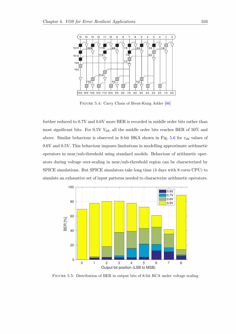
Chapter 4. VOS for Error Resilient Applications 103
Figure 5.4: Carry Chain of Brent-Kung Adder [66]
further reduced to 0.7V and 0.6V more BER is recorded in middle order bits rather than
most significant bits. For 0.5V Vdd, all the middle order bits reaches BER of 50% and
above. Similar behaviour is observed in 8-bit BKA shown in Fig. 5.6 for vdd values of
0.6V and 0.5V. This behaviour imposes limitations in modelling approximate arithmetic
operators in near/sub-threshold using standard models. Behaviour of arithmetic oper-
ators during voltage over-scaling in near/sub-threshold region can be characterized by
SPICE simulations. But SPICE simulators take long time (4 days with 8 cores CPU) to
simulate an exhaustive set of input patterns needed to characterize arithmetic operators.
0 1 2 3 4 5 6 7 8
Output bit position (LSB to MSB)
0
20
40
60
80
100
BE
R [
%]
0.8V
0.7V
0.6V
0.5V
Figure 5.5: Distribution of BER in output bits of 8-bit RCA under voltage scaling

Chapter 4. VOS for Error Resilient Applications 104
0 1 2 3 4 5 6 7 8Output bit position (LSB to MSB)
0
10
20
30
40
50
60
70
80
90
100
BE
R [%
]
0.8V0.7V0.6V0.5V
Figure 5.6: Distribution of BER in output bits of 8-bit BKA under voltage scaling
5.4 Modelling of VOS Arithmetic Operators
As stated previously, there is a need to develop models that can simulate the behavior
of faulty arithmetic operators at the functional level. In this section, we propose a new
modelling technique that is scalable for large-size operators and compliant with different
arithmetic configurations. The proposed model is accurate and allows for fast simula-
tions at the algorithm level by imitating the faulty operator with statistical parameters.
Hardware
Operator
Tclk Vdd Vbb
in1
in2
xin1
in2
CtrlP1,P2,P3,P4
^ x~
Figure 5.7: Functional equivalence for hardware adder
As VOS provokes failures on the longest combinatory datapaths in priority, there is
clearly a link between the impact of the carry propagation path on a given addition and
the error issued from this addition. Fig. 5.7 illustrates the needed relationship between
hardware operator controlled by operating triads and statistical model controlled by
statistical parameters Pi. As the knowledge of the inputs gives necessary information
about the longest carry propagation chain, the values of the inputs are used to generate

Chapter 4. VOS for Error Resilient Applications 105
the statistical parameters that control the equivalent model. These statistical parame-
ters are obtained through an offline optimization process that minimizes the difference
between the outputs of the operator and its equivalent statistical model, according to a
certain metric. In this work, we used three accuracy metrics to calibrate the efficiency
of the proposed statistical model:
• Mean Square Error (MSE) – average of squares of deviations between the output
of the statistical model x and the reference x,
MSE(i) =1
n
n∑i=1
(xi − xi)2 (5.4)
• Hamming distance – number of positions with bit flip between the output of the
statistical model x and the reference x,
dham(i) =
N−1∑j=0
(xi,j ⊕ xi,j) (5.5)
• Weighted Hamming distance – Hamming distance with weight for every bit posi-
tion depending on their significance,
dw ham(i) =N−1∑j=0
(xi,j ⊕ xi,j) .2j (5.6)
5.4.1 Proof of Concept: Modelling of Adders
In the rest of the section, a proof of concept is illustrated by applying VOS on different
adder configurations. All the adder configurations are subjected to VOS and character-
ized using the flow described in Fig. 5.3. Fig. 5.8 shows the design flow of modelling
VOS operators. As shown in Fig. 5.7 rudimentary model of the hardware operators
is created with the input vectors and the statistical parameters. For the given input
vectors, output of both the model and the hardware operator is compared based on the
defined set of accuracy metrics. The comparator shown in Fig. 5.8 generates signal to
noise ratio (SNR) and Hamming distance to determine the quality of the model based
on the accuracy metrics. SNR and Hamming distance are fed back to the optimization
algorithm to further fine tune the model to represent the VOS operator. In the case of
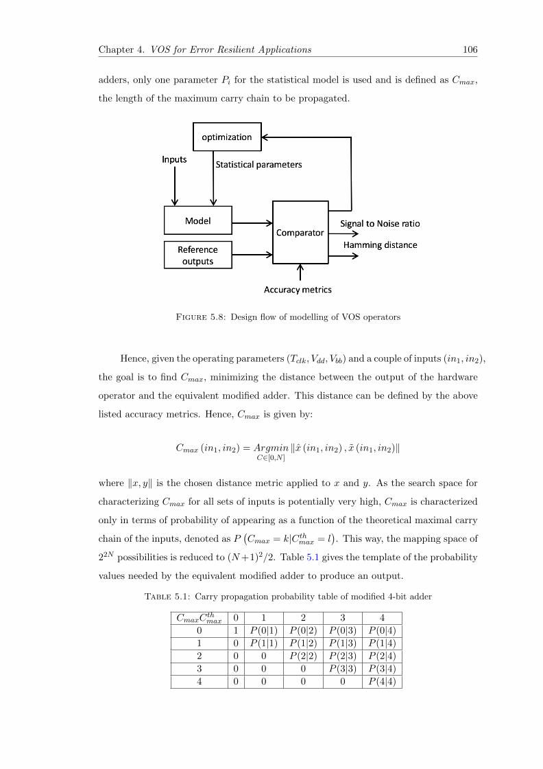
Chapter 4. VOS for Error Resilient Applications 106
adders, only one parameter Pi for the statistical model is used and is defined as Cmax,
the length of the maximum carry chain to be propagated.
Figure 5.8: Design flow of modelling of VOS operators
Hence, given the operating parameters (Tclk, Vdd, Vbb) and a couple of inputs (in1, in2),
the goal is to find Cmax, minimizing the distance between the output of the hardware
operator and the equivalent modified adder. This distance can be defined by the above
listed accuracy metrics. Hence, Cmax is given by:
Cmax (in1, in2) = ArgminC∈[0,N ]
‖x (in1, in2) , x (in1, in2)‖
where ‖x, y‖ is the chosen distance metric applied to x and y. As the search space for
characterizing Cmax for all sets of inputs is potentially very high, Cmax is characterized
only in terms of probability of appearing as a function of the theoretical maximal carry
chain of the inputs, denoted as P(Cmax = k|Cth
max = l). This way, the mapping space of
22N possibilities is reduced to (N+1)2/2. Table 5.1 gives the template of the probability
values needed by the equivalent modified adder to produce an output.
Table 5.1: Carry propagation probability table of modified 4-bit adder
CmaxCthmax 0 1 2 3 4
0 1 P (0|1) P (0|2) P (0|3) P (0|4)
1 0 P (1|1) P (1|2) P (1|3) P (1|4)
2 0 0 P (2|2) P (2|3) P (2|4)
3 0 0 0 P (3|3) P (3|4)
4 0 0 0 0 P (4|4)

Chapter 4. VOS for Error Resilient Applications 107
The optimization algorithm used to construct the modified adder is shown in Al-
gorithm 2. When the inputs (in1, in2) are in the vector of training inputs, output of
the hardware adder configuration x is computed. Based on the particular input pair
(in1, in2), maximum carry chain Cthmax corresponding to the input pair is determined.
Output x of the modified adder with three input parameters (in1, in2, C) is computed.
The distance between the hardware adder output x and modified adder output x is cal-
culated based on the above defined accuracy metrics for different iterations of C. The
flow continues for the entire set of training inputs.
beginP (0 : Nbit adder| 0 : Nbit adder) := 0;max dist := +∞;Cmax temp = 0;for variable in1, in2 ∈ training inputs do
x := add hardware(in1, in2) Cthmax := max carry chain(in1, in2);
for variable C ∈ Cthmax down to 0 do
x := add modified(in1, in2, C);dist := ‖x, x‖;if dist <= max dist then
dist max := dist;Cmax temp := C;
end
end
P (Cmax temp|Cthmax) + +
endP (: | :) := P (: | :)/size(training outputs);
endAlgorithm 2: Optimization Algorithm
After the off-line optimization process is performed, the equivalent modified adder
can be used to generate the outputs corresponding to any couple of inputs in1 and in2.
To imitate the exact operator subjected to VOS triads, the equivalent adder is used in
the following way:
1. Extract the theoretical maximal carry chain Cthmax which would be produced by
the exact addition of in1 and in2.
2. Pick of a random number, choose the corresponding row of the probability table,
in the column representing Cthmax, and assign this value to Cmax.
3. Compute the sum of in1 and in2 with a maximal carry chain limited to Cmax.
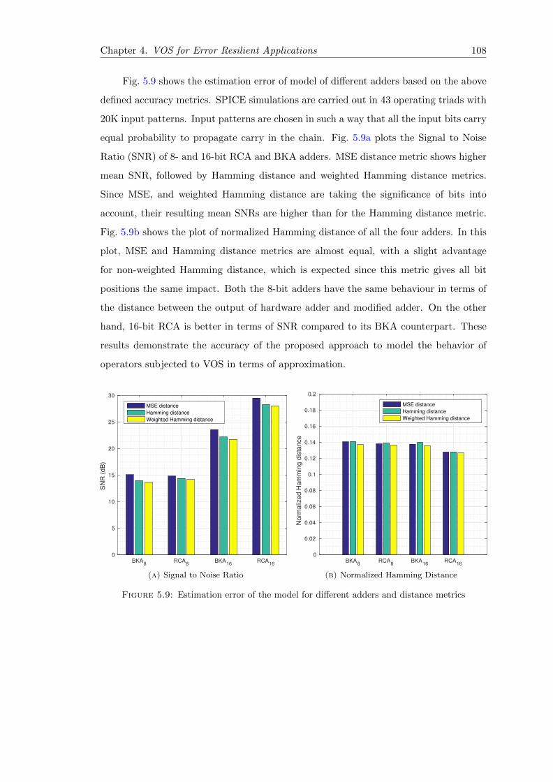
Chapter 4. VOS for Error Resilient Applications 108
Fig. 5.9 shows the estimation error of model of different adders based on the above
defined accuracy metrics. SPICE simulations are carried out in 43 operating triads with
20K input patterns. Input patterns are chosen in such a way that all the input bits carry
equal probability to propagate carry in the chain. Fig. 5.9a plots the Signal to Noise
Ratio (SNR) of 8- and 16-bit RCA and BKA adders. MSE distance metric shows higher
mean SNR, followed by Hamming distance and weighted Hamming distance metrics.
Since MSE, and weighted Hamming distance are taking the significance of bits into
account, their resulting mean SNRs are higher than for the Hamming distance metric.
Fig. 5.9b shows the plot of normalized Hamming distance of all the four adders. In this
plot, MSE and Hamming distance metrics are almost equal, with a slight advantage
for non-weighted Hamming distance, which is expected since this metric gives all bit
positions the same impact. Both the 8-bit adders have the same behaviour in terms of
the distance between the output of hardware adder and modified adder. On the other
hand, 16-bit RCA is better in terms of SNR compared to its BKA counterpart. These
results demonstrate the accuracy of the proposed approach to model the behavior of
operators subjected to VOS in terms of approximation.
BKA8
RCA8
BKA16
RCA16
0
5
10
15
20
25
30
SN
R (
dB
)
MSE distance
Hamming distance
Weighted Hamming distance
(a) Signal to Noise Ratio
BKA8
RCA8
BKA16
RCA16
0
0.02
0.04
0.06
0.08
0.1
0.12
0.14
0.16
0.18
0.2
Norm
aliz
ed H
am
min
g d
ista
nce
MSE distance
Hamming distance
Weighted Hamming distance
(b) Normalized Hamming Distance
Figure 5.9: Estimation error of the model for different adders and distance metrics

Chapter 4. VOS for Error Resilient Applications 109
5.5 Experiments and Results
In our experiments, we characterized 8- and 16-bit ripple carry adder (RCA) and Brent-
Kung adder (BKA) using 28nm-FDSOI technology. Table 5.2 shows the synthesis re-
sults (area, static plus dynamic power, critical path) of different adder configurations.
Post-synthesis SPICE netlist of all the adders are generated and simulated using Eldo
SPICE (version 12.2a). Table 5.3 shows the different operating triads used to simulate
the adders. Clock period (Tclk) of the adders is chosen based on the synthesis timing
report. Supply voltage (Vdd) of all the simulations is scaled down from 1.0V to 0.4V
in steps of 0.1V and body-biasing potential (Vbb) of -2V, 0V, and, 2V. Pattern source
function of SPICE testbench is configured with specific input vectors to test the adder
configurations. The circuit under test is subjected to 20K simulations for every different
operating triad with the same set of input patterns. Energy per operation correspond-
ing to different operating triads is calculated from the simulation results. Output values
generated from the SPICE simulation are compared against the golden (ideal) outputs
corresponding to the input patterns. Automated test scripts calculate various statisti-
cal parameters like BER (ratio of faulty output bits over total output bits), MSE and
bit-wise error probability (ratio of number of faulty bits over total bits in every binary
position) for all the test cases.
Table 5.2: Synthesis Results of 8 and 16 bit RCA and BKA
Benchmarks Area (µm2) Total Power (µW) Critical Path (ns)
8-bit RCA 114.7 170 0.28
8-bit BKA 174.1 267.7 0.19
16-bit RCA 224.5 341 0.53
16-bit BKA 265.5 363.4 0.25
Table 5.3: Operating triads used in Spice simulation
Benchmarks Tclk (ns) Vdd (V) Vbb (V)
8-bit RCA 0.5, 0.28, 0.19, 0.13 1 to 0.4 -2 to 2
8-bit BKA 0.5, 0.19, 0.13, 0.064 1 to 0.4 -2 to 2
16-bit RCA 0.7, 0.53, 0.25, 0.20 1 to 0.4 -2 to 2
16-bit BKA 0.7, 0.25, 0.20, 0.15 1 to 0.4 -2 to 2
Fig. 5.10 and Fig. 5.11 show the plots of BER vs Energy/Operation of 8-bit RCA
and BKA adders. Likewise, plots of BER vs Energy/Operation of 16-bit RCA and BKA
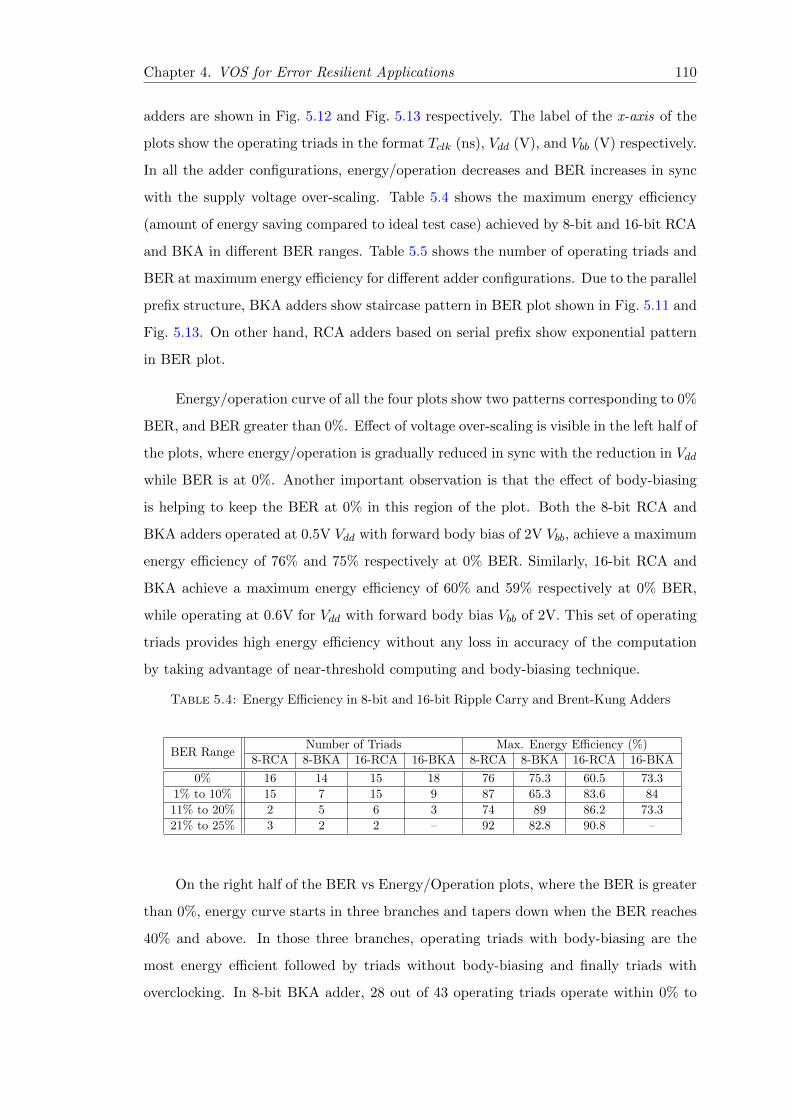
Chapter 4. VOS for Error Resilient Applications 110
adders are shown in Fig. 5.12 and Fig. 5.13 respectively. The label of the x-axis of the
plots show the operating triads in the format Tclk (ns), Vdd (V), and Vbb (V) respectively.
In all the adder configurations, energy/operation decreases and BER increases in sync
with the supply voltage over-scaling. Table 5.4 shows the maximum energy efficiency
(amount of energy saving compared to ideal test case) achieved by 8-bit and 16-bit RCA
and BKA in different BER ranges. Table 5.5 shows the number of operating triads and
BER at maximum energy efficiency for different adder configurations. Due to the parallel
prefix structure, BKA adders show staircase pattern in BER plot shown in Fig. 5.11 and
Fig. 5.13. On other hand, RCA adders based on serial prefix show exponential pattern
in BER plot.
Energy/operation curve of all the four plots show two patterns corresponding to 0%
BER, and BER greater than 0%. Effect of voltage over-scaling is visible in the left half of
the plots, where energy/operation is gradually reduced in sync with the reduction in Vdd
while BER is at 0%. Another important observation is that the effect of body-biasing
is helping to keep the BER at 0% in this region of the plot. Both the 8-bit RCA and
BKA adders operated at 0.5V Vdd with forward body bias of 2V Vbb, achieve a maximum
energy efficiency of 76% and 75% respectively at 0% BER. Similarly, 16-bit RCA and
BKA achieve a maximum energy efficiency of 60% and 59% respectively at 0% BER,
while operating at 0.6V for Vdd with forward body bias Vbb of 2V. This set of operating
triads provides high energy efficiency without any loss in accuracy of the computation
by taking advantage of near-threshold computing and body-biasing technique.
Table 5.4: Energy Efficiency in 8-bit and 16-bit Ripple Carry and Brent-Kung Adders
BER RangeNumber of Triads Max. Energy Efficiency (%)
8-RCA 8-BKA 16-RCA 16-BKA 8-RCA 8-BKA 16-RCA 16-BKA
0% 16 14 15 18 76 75.3 60.5 73.3
1% to 10% 15 7 15 9 87 65.3 83.6 84
11% to 20% 2 5 6 3 74 89 86.2 73.3
21% to 25% 3 2 2 – 92 82.8 90.8 –
On the right half of the BER vs Energy/Operation plots, where the BER is greater
than 0%, energy curve starts in three branches and tapers down when the BER reaches
40% and above. In those three branches, operating triads with body-biasing are the
most energy efficient followed by triads without body-biasing and finally triads with
overclocking. In 8-bit BKA adder, 28 out of 43 operating triads operate within 0% to
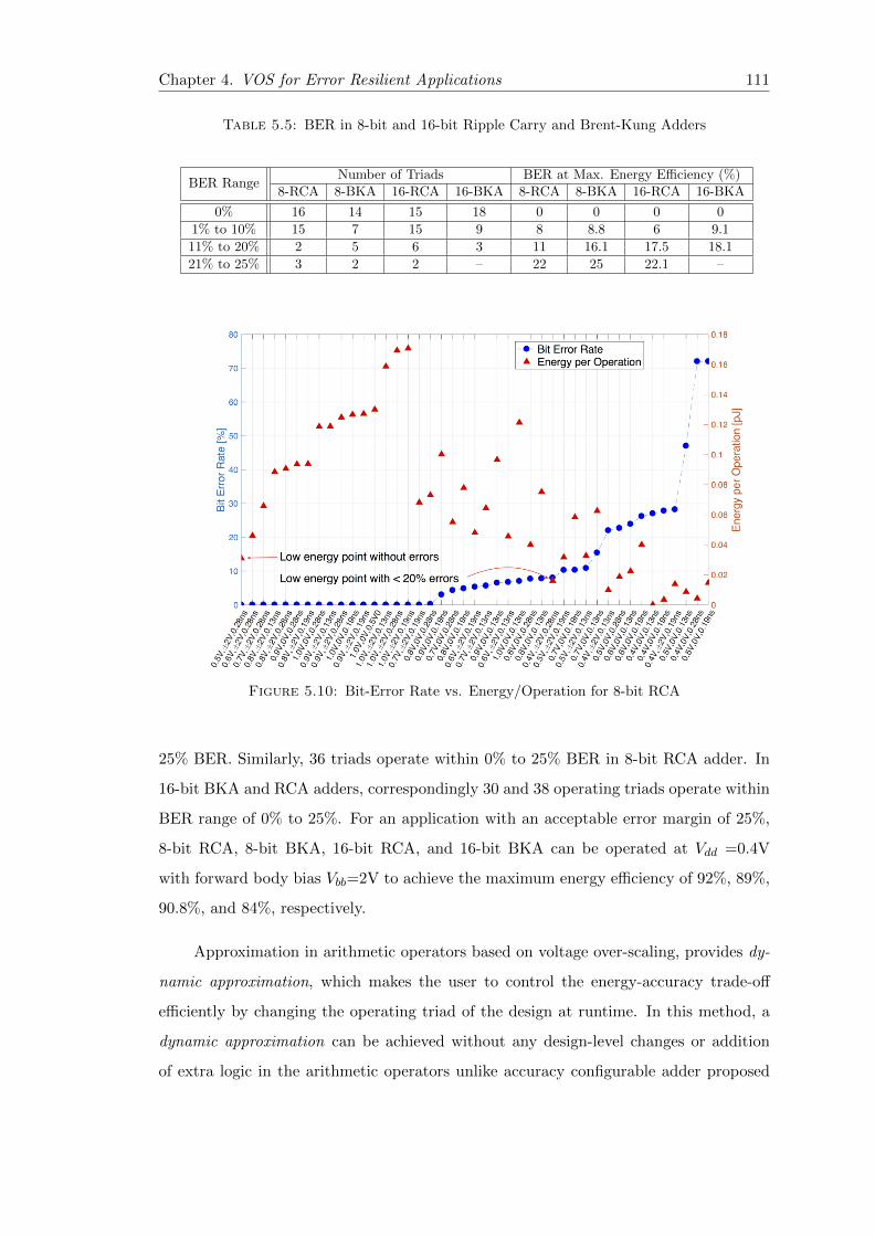
Chapter 4. VOS for Error Resilient Applications 111
Table 5.5: BER in 8-bit and 16-bit Ripple Carry and Brent-Kung Adders
BER RangeNumber of Triads BER at Max. Energy Efficiency (%)
8-RCA 8-BKA 16-RCA 16-BKA 8-RCA 8-BKA 16-RCA 16-BKA
0% 16 14 15 18 0 0 0 0
1% to 10% 15 7 15 9 8 8.8 6 9.1
11% to 20% 2 5 6 3 11 16.1 17.5 18.1
21% to 25% 3 2 2 – 22 25 22.1 –
Figure 5.10: Bit-Error Rate vs. Energy/Operation for 8-bit RCA
25% BER. Similarly, 36 triads operate within 0% to 25% BER in 8-bit RCA adder. In
16-bit BKA and RCA adders, correspondingly 30 and 38 operating triads operate within
BER range of 0% to 25%. For an application with an acceptable error margin of 25%,
8-bit RCA, 8-bit BKA, 16-bit RCA, and 16-bit BKA can be operated at Vdd =0.4V
with forward body bias Vbb=2V to achieve the maximum energy efficiency of 92%, 89%,
90.8%, and 84%, respectively.
Approximation in arithmetic operators based on voltage over-scaling, provides dy-
namic approximation, which makes the user to control the energy-accuracy trade-off
efficiently by changing the operating triad of the design at runtime. In this method, a
dynamic approximation can be achieved without any design-level changes or addition
of extra logic in the arithmetic operators unlike accuracy configurable adder proposed
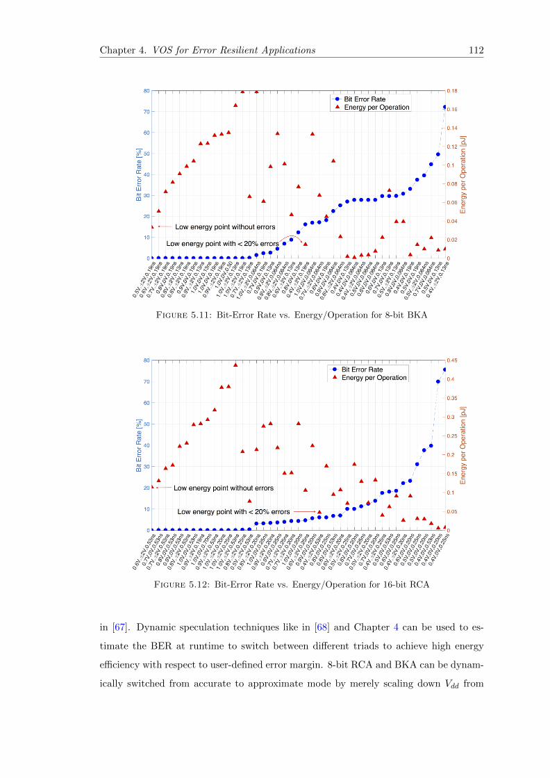
Chapter 4. VOS for Error Resilient Applications 112
Figure 5.11: Bit-Error Rate vs. Energy/Operation for 8-bit BKA
Figure 5.12: Bit-Error Rate vs. Energy/Operation for 16-bit RCA
in [67]. Dynamic speculation techniques like in [68] and Chapter 4 can be used to es-
timate the BER at runtime to switch between different triads to achieve high energy
efficiency with respect to user-defined error margin. 8-bit RCA and BKA can be dynam-
ically switched from accurate to approximate mode by merely scaling down Vdd from
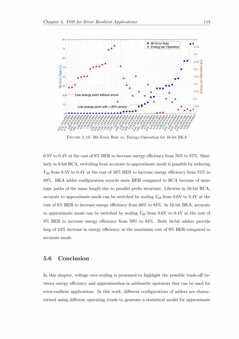
Chapter 4. VOS for Error Resilient Applications 113
Figure 5.13: Bit-Error Rate vs. Energy/Operation for 16-bit BKA
0.5V to 0.4V at the cost of 8% BER to increase energy efficiency from 76% to 87%. Simi-
larly in 8-bit RCA, switching from accurate to approximate mode is possible by reducing
Vdd from 0.5V to 0.4V at the cost of 16% BER to increase energy efficiency from 75% to
89%. BKA adder configuration records more BER compared to RCA because of more
logic paths of the same length due to parallel prefix structure. Likewise in 16-bit RCA,
accurate to approximate mode can be switched by scaling Vdd from 0.6V to 0.4V at the
cost of 6% BER to increase energy efficiency from 60% to 84%. In 16-bit BKA, accurate
to approximate mode can be switched by scaling Vdd from 0.6V to 0.4V at the cost of
9% BER to increase energy efficiency from 59% to 84%. Both 16-bit adders provide
leap of 24% increase in energy efficiency at the maximum cost of 9% BER compared to
accurate mode.
5.6 Conclusion
In this chapter, voltage over-scaling is presented to highlight the possible trade-off be-
tween energy efficiency and approximation in arithmetic operators that can be used for
error-resilient applications. In this work, different configurations of adders are charac-
terized using different operating triads to generate a statistical model for approximate
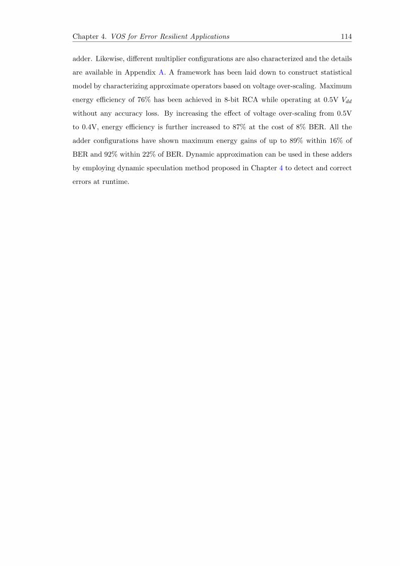
Chapter 4. VOS for Error Resilient Applications 114
adder. Likewise, different multiplier configurations are also characterized and the details
are available in Appendix A. A framework has been laid down to construct statistical
model by characterizing approximate operators based on voltage over-scaling. Maximum
energy efficiency of 76% has been achieved in 8-bit RCA while operating at 0.5V Vdd
without any accuracy loss. By increasing the effect of voltage over-scaling from 0.5V
to 0.4V, energy efficiency is further increased to 87% at the cost of 8% BER. All the
adder configurations have shown maximum energy gains of up to 89% within 16% of
BER and 92% within 22% of BER. Dynamic approximation can be used in these adders
by employing dynamic speculation method proposed in Chapter 4 to detect and correct
errors at runtime.

Chapter 6
Energy Estimation Framework for
VLIW Processors
6.1 Introduction
High performance at low power consumption has been the primary requirement in con-
tinuously evolving processor architectures. Parallelism has been the way to achieve high
performance in processor architectures by splitting a task into multiple tinier chunks
and executing them in parallel. Parallelism can be broadly classified into Hardware Par-
allelism and Software Parallelism. In simple terms, hardware parallelism is achieved by
hardware multiplicity and sophisticated architecture. Hardware parallelism offers high
performance at the cost of high silicon footprint. Advancement in fabrication technolo-
gies and reduction in feature size have made it possible to put even 100+ cores in general
purpose processors. Hardware parallelism is implemented in different ways like pipelin-
ing, multi-core system, multiprocessor systems, etc. In a uni-processor environment,
architectures like Pipelining, Superscalar, VLIW (Very Long Instruction Word) are the
common form of hardware parallelism. A conventional processor would take multiple
cycles to compute an instruction. Present day processors can issue multiple instructions
per cycle. This increases the execution speed, thereby increasing the throughput of the
processor multifold. A multiprocessor system with n processors, each processor capa-
ble of issuing m instructions per cycle, has the capability to compute nm threads of
instructions in parallel.
115
Chapter 5. Energy Estimation Framework for VLIW Processors 116
To exploit the potential of hardware parallelism, software should support paral-
lelism as well. Software parallelism is defined by the dependence of control and data
in programs. Instruction Level Parallelism (ILP) is defined as number of instructions
that can be executed simultaneously. ILP can be implemented either at hardware or
software level. At the hardware level, the processor performs dynamic parallelism by
deciding at runtime which instructions to execute in parallel. On the other hand, at
the software level, the compiler performs static parallelism during compilation time.
For applications like image and video processing, graphics, data mining, etc., there is a
scope for high level of parallelism at instruction level. Also, these applications have the
tendency to tolerate errors in computation, thereby allowing deliberate approximations
in the computing. Earlier chapters discussed in detail the advantages and challenges
in approximate computing in the context of near-threshold regime. In Chapter 5, the
need for statistical models to represent the behaviour of arithmetic operators was also
discussed.
In the rest of the chapter, scope for approximation in VLIW platform is discussed.
A framework is formulated to estimate energy vs accuracy trade-offs of the execution
unit of ρ− V EX VLIW processor [69].
6.2 VLIW Processor Architecture
An VLIW is a processor architecture designed to exploit instruction level parallelism.
Processor architecture based on pipelining can provide parallelism by partial overlap of
instructions. Superscalar architecture evolved over pipelining architecture and execute
two or more consecutive instructions in parallel. Parallelism of Superscalar is limited
to data independent instructions. Pipelining architecture follows In-Order execution
where instructions are executed in the order they appear in the program. Most of the
time, consecutive instructions are not independent, which limits the parallelism offered
by pipelining. To fully exploit the benefits of parallelism, instructions have to be exe-
cuted based on data flow not in the order they appear in the program. This style of
execution is called Out-of-Order execution. In Out-of-Order execution, the processor
examines the instruction window of the consecutive instructions in re-order buffer. In-
dependent instructions in instruction window with readily available data are executed
by the processor. Superscalar architecture follows both In-Order (ex. PowerPC 604e)
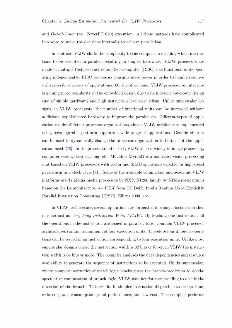
Chapter 5. Energy Estimation Framework for VLIW Processors 117
and Out-of-Order (ex. PowerPC 620) execution. All these methods have complicated
hardware to make the decisions internally to achieve parallelism.
In contrast, VLIW shifts the complexity to the compiler in deciding which instruc-
tions to be executed in parallel, resulting in simpler hardware. VLIW processors are
made of multiple Reduced Instruction Set Computer (RISC) like functional units oper-
ating independently. RISC processors consume more power in order to handle resource
utilization for a variety of applications. On the other hand, VLIW processor architecture
is gaining more popularity in the embedded design due to its inherent low-power design
(use of simple hardware) and high instruction level parallelism. Unlike superscalar de-
signs, in VLIW processors, the number of functional units can be increased without
additional sophisticated hardware to improve the parallelism. Different types of appli-
cation require different processor organizations, thus a VLIW architecture implemented
using reconfigurable platform supports a wide range of applications. Generic binaries
can be used to dynamically change the processor organization to better suit the appli-
cation need [70]. In the present trend of IoT, VLIW is used widely in image processing,
computer vision, deep learning, etc. Movidius Myriad2 is a manycore vision processing
unit based on VLIW processors with vector and SIMD operations capable for high speed
parallelism in a clock cycle [71]. Some of the available commercial and academic VLIW
platforms are TriMedia media processors by NXP, ST200 family by STMicroelectronics
based on the Lx architecture, ρ−V EX from TU Delft, Intel’s Itanium IA-64 Explicitly
Parallel Instruction Computing (EPIC), Elbrus 2000, etc.
In VLIW architecture, several operations are formatted in a single instruction thus
it is termed as Very Long Instruction Word (VLIW). By fetching one instruction, all
the operations in the instruction are issued in parallel. Most common VLIW processor
architectures contain a minimum of four execution units. Therefore four different opera-
tions can be issued in an instruction corresponding to four execution units. Unlike most
superscalar designs where the instruction width is 32 bits or fewer, in VLIW the instruc-
tion width is 64 bits or more. The compiler analyses the data dependencies and resource
availability to generate the sequence of instructions to be executed. Unlike superscalar,
where complex instruction-dispatch logic blocks guess the branch-prediction to do the
speculative computation of branch logic, VLIW uses heuristic or profiling to decide the
direction of the branch. This results in simpler instruction-dispatch, less design time,
reduced power consumption, good performance, and low cost. The compiler performs
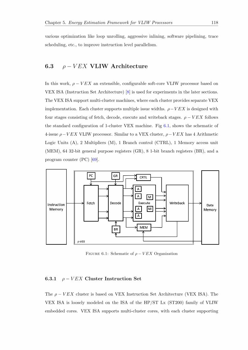
Chapter 5. Energy Estimation Framework for VLIW Processors 118
various optimization like loop unrolling, aggressive inlining, software pipelining, trace
scheduling, etc., to improve instruction level parallelism.
6.3 ρ− V EX VLIW Architecture
In this work, ρ − V EX an extensible, configurable soft-core VLIW processor based on
VEX ISA (Instruction Set Architecture) [8] is used for experiments in the later sections.
The VEX ISA support multi-cluster machines, where each cluster provides separate VEX
implementation. Each cluster supports multiple issue widths. ρ−V EX is designed with
four stages consisting of fetch, decode, execute and writeback stages. ρ− V EX follows
the standard configuration of 1-cluster VEX machine. Fig 6.1, shows the schematic of
4-issue ρ−V EX VLIW processor. Similar to a VEX cluster, ρ−V EX has 4 Arithmetic
Logic Units (A), 2 Multipliers (M), 1 Branch control (CTRL), 1 Memory access unit
(MEM), 64 32-bit general purpose registers (GR), 8 1-bit branch registers (BR), and a
program counter (PC) [69].
Figure 6.1: Schematic of ρ− V EX Organization
6.3.1 ρ− V EX Cluster Instruction Set
The ρ − V EX cluster is based on VEX Instruction Set Architecture (VEX ISA). The
VEX ISA is loosely modeled on the ISA of the HP/ST Lx (ST200) family of VLIW
embedded cores. VEX ISA supports multi-cluster cores, with each cluster supporting
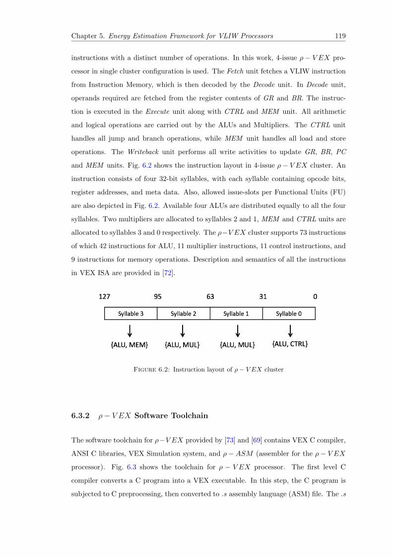
Chapter 5. Energy Estimation Framework for VLIW Processors 119
instructions with a distinct number of operations. In this work, 4-issue ρ − V EX pro-
cessor in single cluster configuration is used. The Fetch unit fetches a VLIW instruction
from Instruction Memory, which is then decoded by the Decode unit. In Decode unit,
operands required are fetched from the register contents of GR and BR. The instruc-
tion is executed in the Execute unit along with CTRL and MEM unit. All arithmetic
and logical operations are carried out by the ALUs and Multipliers. The CTRL unit
handles all jump and branch operations, while MEM unit handles all load and store
operations. The Writeback unit performs all write activities to update GR, BR, PC
and MEM units. Fig. 6.2 shows the instruction layout in 4-issue ρ− V EX cluster. An
instruction consists of four 32-bit syllables, with each syllable containing opcode bits,
register addresses, and meta data. Also, allowed issue-slots per Functional Units (FU)
are also depicted in Fig. 6.2. Available four ALUs are distributed equally to all the four
syllables. Two multipliers are allocated to syllables 2 and 1, MEM and CTRL units are
allocated to syllables 3 and 0 respectively. The ρ−V EX cluster supports 73 instructions
of which 42 instructions for ALU, 11 multiplier instructions, 11 control instructions, and
9 instructions for memory operations. Description and semantics of all the instructions
in VEX ISA are provided in [72].
Figure 6.2: Instruction layout of ρ− V EX cluster
6.3.2 ρ− V EX Software Toolchain
The software toolchain for ρ−V EX provided by [73] and [69] contains VEX C compiler,
ANSI C libraries, VEX Simulation system, and ρ− ASM (assembler for the ρ− V EX
processor). Fig. 6.3 shows the toolchain for ρ − V EX processor. The first level C
compiler converts a C program into a VEX executable. In this step, the C program is
subjected to C preprocessing, then converted to .s assembly language (ASM) file. The .s

Chapter 5. Energy Estimation Framework for VLIW Processors 120
file is fed to compiled simulator environment, where .s file is converted to .cs file. Host C
compiler processes the .cs file and generates host object files. Host linker links simulation
support library, cache simulation library, VEX C library, and application object files.
At the end, a VEX executable is generated that can be executed by invoking it.
Figure 6.3: Toolchain for ρ− V EX processor
In the flow of compilation and simulation, the intermediary files like VEX assembly
file (.s) and compiled-simulator translated file (.cs.c) are generally masked and the final
VEX executable is created. In addition to the standard semantic of the instructions,
.cs file also contains other interesting statistics and information can be used to estimate
energy consumption at the instruction level. The VEX compiler uses trace scheduling in
optimization phase. In trace scheduling, loops are converted into a sequence of codes by
using loop unrolling and static branch prediction. By default VEX compiler performs
-O2 optimization, meaning minimal loop unrolling and trace scheduling. The .s shows
the profile of trace scheduling, which can be used to understand the flow of execution.
In the command line interface of the VEX C compiler -mas g flag and -S attributes are
used to output .cs.c and .s intermediary files.

Chapter 5. Energy Estimation Framework for VLIW Processors 121
6.4 Power and Energy Estimation in VLIW processors
Estimating energy is an important and necessary step to efficiently utilize VLIW proces-
sors. This allows the designer to manage hardware and software parallelism to achieve
high energy efficiency with maximum performance. Estimating energy consumption at
instruction level will provide a clear understanding of energy consumption by different
modules of a cluster at different configurations. In literature, different levels of power
estimation techniques for microprocessors are proposed to efficiently evaluate the soft-
ware in terms of power consumption. Power estimation is broadly classified as follows
based on different abstractions:
• System Level
• Instruction Level
• Micro-architecture Level
• RT Level
• Gate Level
• Transistor Level
Power estimation methods from system level to micro-architectural level are less accurate
but faster than gate-level and RT-level power estimations. In literature, almost all
of the power estimation techniques are based on Instruction-Level power models. At
instruction level, power estimation is simpler, faster, and also provides enough details
to under the behaviour of different modules of the processor.
6.4.1 Instruction-Level Power Estimation
Instruction-level power estimation (ILEP) provides a clear understanding of power cost
vs. software implementation in a microprocessor system. Once the power models are
generated, power estimation for any application can be obtained by simple C compilers.
Also, it helps to make best design decisions at higher abstraction level [74]. Instruction-
level power consumption technique is based on measuring the current drawn by the
processor while it executes certain instructions repeatedly. Based on the current con-
sumption pattern, power models are designed to represent the execution behaviour of
Chapter 5. Energy Estimation Framework for VLIW Processors 122
the processor for any particular instruction [75]. This method is very accurate and uses
linear regression with instruction and architectural level variables such as average bit
switching activity in the instruction register, address bus, etc. [74]. Another way of
generating power models is discussed in [76] by estimating power cost for modules based
on average capacitance that would switch when the given module is activated. Once the
power costs for different modules like ALU, control units, and memory are determined,
average power consumption of instructions using these modules are computed by simple
arithmetic.
In general, power models described above are proposed for hardcore processors
like Intel 486DX2, Intel i960 family, etc. Most of the power models provide estimation
on the average power consumption of the processor for a given application. Based
on those estimations, the designer can modify the hardware configuration or software
parameters to reduce the power consumption of any given program. These methods
lack the dynamicity to provide power consumption for different configurations at the
same time, so the user has to repeat the process to estimate average power for different
configurations. When considering VLIW processors, traditional instruction-level power
modeling approaches imply new challenges because of varying issue width capability in
VLIW processors [77]. Also, estimation based on power model at instruction-level lacks
insight on the causes of power consumption within the cluster [78]. This limitation is
addressed in [79] by generating power models at the micro-architectural level rather than
at instruction-level.
In [74], gate-level energy models are presented to do instruction level power analysis.
In this method, two different implementations of the microcontroller are studied. The
energy consumption of each instruction is different in each of those implementations.
By studying these differences and data correlation on the energy consumption of those
instructions, parts of the design can be resynthesized for low power application. Based on
the energy estimates of few instructions, energy consumption of few sample programs
are predicted. In [80], analytical energy models are proposed to estimate the energy
consumption of a nested loop executed on a VLIW ASIP for different vector widths. In
this energy model, energy consumption is estimated for a vector computing unit and
program as a function of vector width. The total energy of an instruction for any given

Chapter 5. Energy Estimation Framework for VLIW Processors 123
vector width w is represented as
Et(w) = Ed(w) + Es(w) (6.1)
where Ed(w) is dynamic energy spent in data path and Es(w) is static energy that
depends on program execution time.
In [77], an energy model of a VLIW processor at instruction-level with the accuracy
of the micro-architectural level is proposed. On contrast to traditional energy model,
where instruction energy for each given clock cycle is estimated without considering the
other instruction in the pipeline, the pipeline-aware method proposed in [77] considers
the overlapping of instructions and estimates more accurate energy consumption. The
estimation of energy consumed by the processor during the execution of the sequence w
with N instructions is expressed as
E(w) =∑∀n∈N
(E(wn | wn−1) + Ec + co) (6.2)
where E(wn | wn−1) is the energy dissipated by the data path associated with the execu-
tion of instruction wn, Ec is the total energy dissipated by the control unit and co is the
energy constant associated with start-up sequence of the processor. Energy dissipated
by instruction wn is estimated by considering the overlap of previous instruction wn−1
in the pipeline.
In [78], power models for instruction-level power estimation with RTL-level accu-
racy are proposed. In this method, the average energy consumption of an instruction
wn is
E(wn) = B + αn × csyl +m× p× S + l × q ×M (6.3)
where B is the average energy base cost (while executing NOPs), αn is the number of syl-
lables different from NOPs, csyl is average energy consumption associated with execution
of a syllable. The third term is the summation of additive average energy consumption
due to a miss event on the D-cache. The fourth term is related to I-cache misses. Simi-
lar approach is used in [81], where the base energy is associated with execution of NOP
energy and incremental energy is added for each of the instructions in the execution set.
The inter execution-set is modeled as linear equations to represent functional to func-
tional instruction switching, function to NOP switching, and variability in the length

Chapter 5. Energy Estimation Framework for VLIW Processors 124
of execution. In [82], power models in [78] are improved to estimate inter-instruction
energy consumption by characterizing each operation in isolation, then by clustering
operations considering their average energy cost known as instruction clustering.
All these power macro-models used to estimate energy consumption at instruction-
level are developed in the context of standard (normal) operating conditions. For pro-
cessor designs with ultra-low power techniques like voltage over-scaling the traditional
power models lack the capability to estimate instruction-level energy consumption where
the supply voltage is dynamically changed to counter the variability effects. Also, in
near-threshold regime, energy metric is predominately used to measure the gains of
voltage scaling techniques. This demands a need for an energy estimation method for
VLIW processors in the scope of near-threshold regime.
In the rest of the chapter, an instruction-level energy estimation method for ex-
ecution unit of ρ − V EX cluster is presented. In this work, the energy estimation is
in the context of near-threshold regime and approximate computing. Therefore, along
with energy metric, error metric is also estimated to highlight the reduction in accuracy.
Energy estimation at high abstraction level are much faster than transistor-level based
estimation methods. But the higher abstraction level energy estimations lack the accu-
racy when compared to transistor-level. On average, gate-level energy estimations are
10% to 15% less accurate than the transistor-level estimations [83]. Primary objective of
this work is to propose a framework to estimate energy consumption of execution unit of
ρ−V EX cluster with the accuracy of transistor-level and at the speed of instruction-level
methods.
6.5 Energy Estimation in ρ− V EX processor
The execution unit of ρ − V EX cluster consists of 4 ALUs and 2 Multipliers. Fig 6.4
shows the block diagram of 32-bit ALU, and Multiplier (MUL) in the ρ−V EX cluster of
Fig 6.1. Different operations of the ALU and MUL are chosen by 6-bit opcodes, alu op
and mul op respectively. In this work, instruction level energy estimation is done in two
phases as follows.
• Characterization: In this phase to obtain RT-level accuracy, the execution unit of
ρ− V EX cluster is characterized for different operating triads.

Chapter 5. Energy Estimation Framework for VLIW Processors 125
Figure 6.4: Block diagram of ALU and MUL units in ρ− V EX cluster
• Estimation: Based on the characterization of the execution unit, energy estimation
is done using C compiler for different instructions for different operating modes.
6.5.1 Characterization of Execution Unit in ρ− V EX Cluster
To determine accurate energy consumption by the module like ALUs and Multipliers,
the execution unit of ρ − V EX cluster is characterized based on SPICE simulation.
Fig. 6.5, shows the schematic of characterization process of the execution unit. In this
method, HDL description of the execution unit is synthesized using Synopsys Design
Compiler (version H-2013.03-SP5-2). Inherent low leakage FDSOI 28nm design library
and user-defined timing constraints are used to synthesize the execution unit.
Figure 6.5: Schematic of characterization of execution unit of ρ− V EX cluster
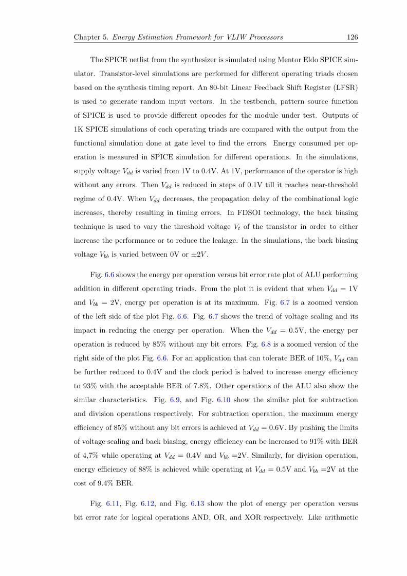
Chapter 5. Energy Estimation Framework for VLIW Processors 126
The SPICE netlist from the synthesizer is simulated using Mentor Eldo SPICE sim-
ulator. Transistor-level simulations are performed for different operating triads chosen
based on the synthesis timing report. An 80-bit Linear Feedback Shift Register (LFSR)
is used to generate random input vectors. In the testbench, pattern source function
of SPICE is used to provide different opcodes for the module under test. Outputs of
1K SPICE simulations of each operating triads are compared with the output from the
functional simulation done at gate level to find the errors. Energy consumed per op-
eration is measured in SPICE simulation for different operations. In the simulations,
supply voltage Vdd is varied from 1V to 0.4V. At 1V, performance of the operator is high
without any errors. Then Vdd is reduced in steps of 0.1V till it reaches near-threshold
regime of 0.4V. When Vdd decreases, the propagation delay of the combinational logic
increases, thereby resulting in timing errors. In FDSOI technology, the back biasing
technique is used to vary the threshold voltage Vt of the transistor in order to either
increase the performance or to reduce the leakage. In the simulations, the back biasing
voltage Vbb is varied between 0V or ±2V .
Fig. 6.6 shows the energy per operation versus bit error rate plot of ALU performing
addition in different operating triads. From the plot it is evident that when Vdd = 1V
and Vbb = 2V, energy per operation is at its maximum. Fig. 6.7 is a zoomed version
of the left side of the plot Fig. 6.6. Fig. 6.7 shows the trend of voltage scaling and its
impact in reducing the energy per operation. When the Vdd = 0.5V, the energy per
operation is reduced by 85% without any bit errors. Fig. 6.8 is a zoomed version of the
right side of the plot Fig. 6.6. For an application that can tolerate BER of 10%, Vdd can
be further reduced to 0.4V and the clock period is halved to increase energy efficiency
to 93% with the acceptable BER of 7.8%. Other operations of the ALU also show the
similar characteristics. Fig. 6.9, and Fig. 6.10 show the similar plot for subtraction
and division operations respectively. For subtraction operation, the maximum energy
efficiency of 85% without any bit errors is achieved at Vdd = 0.6V. By pushing the limits
of voltage scaling and back biasing, energy efficiency can be increased to 91% with BER
of 4,7% while operating at Vdd = 0.4V and Vbb =2V. Similarly, for division operation,
energy efficiency of 88% is achieved while operating at Vdd = 0.5V and Vbb =2V at the
cost of 9.4% BER.
Fig. 6.11, Fig. 6.12, and Fig. 6.13 show the plot of energy per operation versus
bit error rate for logical operations AND, OR, and XOR respectively. Like arithmetic
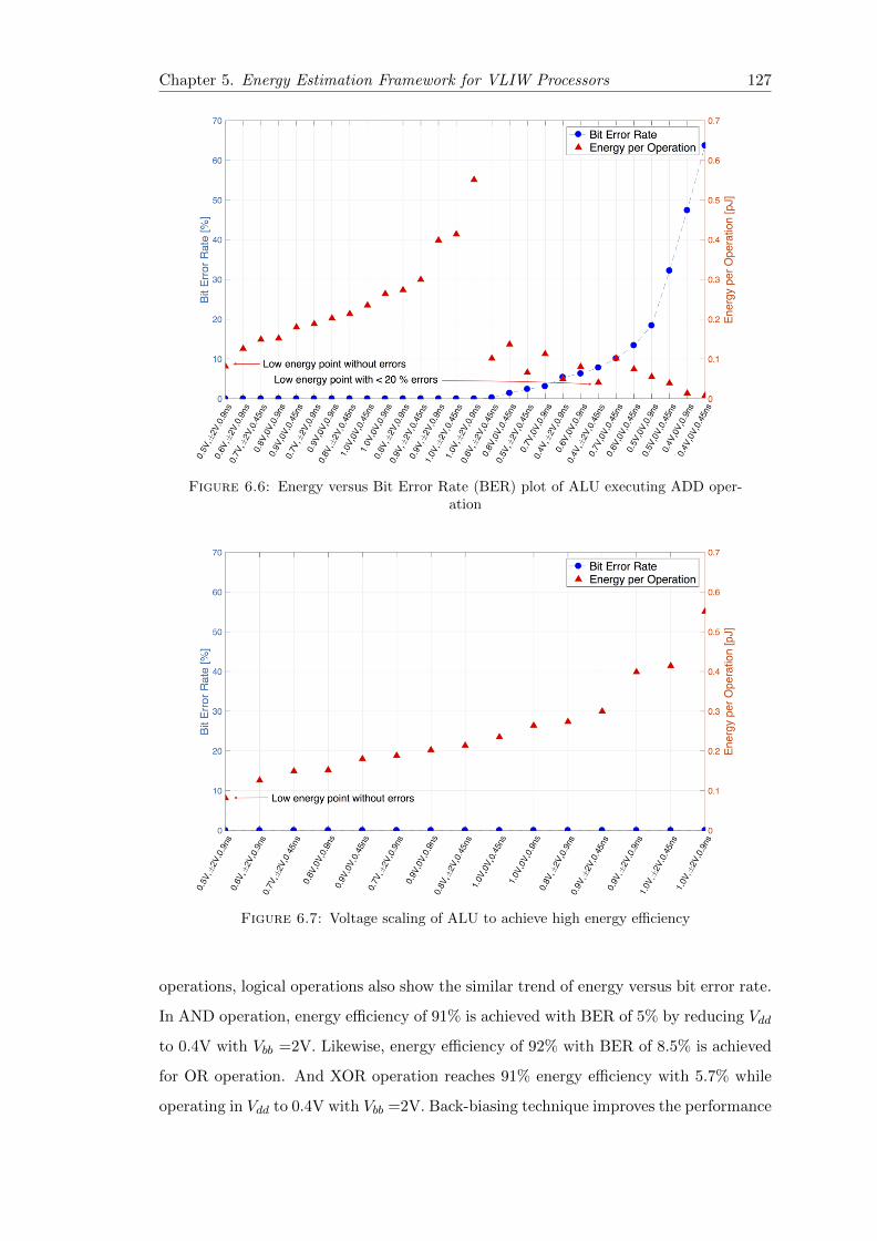
Chapter 5. Energy Estimation Framework for VLIW Processors 127
Figure 6.6: Energy versus Bit Error Rate (BER) plot of ALU executing ADD oper-ation
Figure 6.7: Voltage scaling of ALU to achieve high energy efficiency
operations, logical operations also show the similar trend of energy versus bit error rate.
In AND operation, energy efficiency of 91% is achieved with BER of 5% by reducing Vdd
to 0.4V with Vbb =2V. Likewise, energy efficiency of 92% with BER of 8.5% is achieved
for OR operation. And XOR operation reaches 91% energy efficiency with 5.7% while
operating in Vdd to 0.4V with Vbb =2V. Back-biasing technique improves the performance
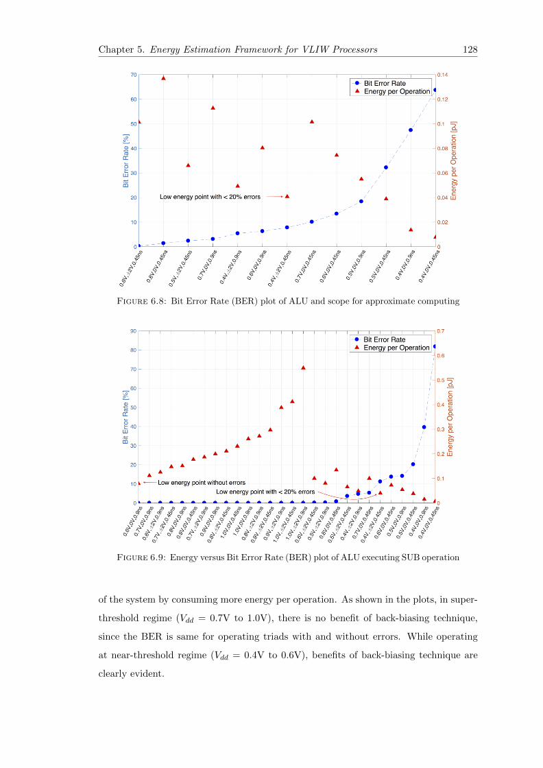
Chapter 5. Energy Estimation Framework for VLIW Processors 128
Figure 6.8: Bit Error Rate (BER) plot of ALU and scope for approximate computing
Figure 6.9: Energy versus Bit Error Rate (BER) plot of ALU executing SUB operation
of the system by consuming more energy per operation. As shown in the plots, in super-
threshold regime (Vdd = 0.7V to 1.0V), there is no benefit of back-biasing technique,
since the BER is same for operating triads with and without errors. While operating
at near-threshold regime (Vdd = 0.4V to 0.6V), benefits of back-biasing technique are
clearly evident.

Chapter 5. Energy Estimation Framework for VLIW Processors 129
Figure 6.10: Energy versus Bit Error Rate (BER) plot of ALU executing DIV oper-ation
The existing energy and power models for instruction level energy/power estima-
tion of VLIW platforms are not developed in the context of near-threshold regime. This
limitation reduces the usability of such models for applications like image and video
processing, data mining, etc., where there is a scope for scaling the supply voltage to
near-threshold regime to extract higher energy efficiency with the cost of acceptable
timing errors as defined by the user. The proposed characterization method is used
to characterize the behaviour of the execution unit of ρ − V EX cluster for a variety
of instructions and for different operating triads. With the extracted energy and error
information for various operations, instruction-level energy can be estimated by formu-
lating a framework for benchmark programs based on C language.
6.5.2 Proposed Instruction-level Energy Estimation Method
In this work, we propose functionality based energy estimation method. Energy con-
sumption of different instructions are estimated based on the characterization of ex-
ecution unit of ρ − V EX cluster discussed in the previous section. Fig. 6.14 shows
the execution unit (highlighted) of the ρ − V EX cluster. In general, execution of an
instruction happens in different pipeline stages like fetch, decode, execute, and write-
back. Energy consumed by each of these stages are denoted as Efetch, Edecode, Etotexec,
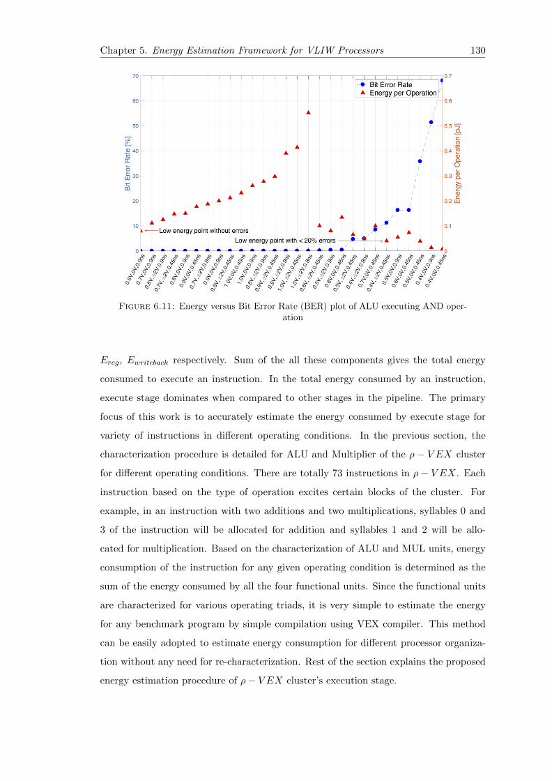
Chapter 5. Energy Estimation Framework for VLIW Processors 130
Figure 6.11: Energy versus Bit Error Rate (BER) plot of ALU executing AND oper-ation
Ereg, Ewriteback respectively. Sum of the all these components gives the total energy
consumed to execute an instruction. In the total energy consumed by an instruction,
execute stage dominates when compared to other stages in the pipeline. The primary
focus of this work is to accurately estimate the energy consumed by execute stage for
variety of instructions in different operating conditions. In the previous section, the
characterization procedure is detailed for ALU and Multiplier of the ρ − V EX cluster
for different operating conditions. There are totally 73 instructions in ρ− V EX. Each
instruction based on the type of operation excites certain blocks of the cluster. For
example, in an instruction with two additions and two multiplications, syllables 0 and
3 of the instruction will be allocated for addition and syllables 1 and 2 will be allo-
cated for multiplication. Based on the characterization of ALU and MUL units, energy
consumption of the instruction for any given operating condition is determined as the
sum of the energy consumed by all the four functional units. Since the functional units
are characterized for various operating triads, it is very simple to estimate the energy
for any benchmark program by simple compilation using VEX compiler. This method
can be easily adopted to estimate energy consumption for different processor organiza-
tion without any need for re-characterization. Rest of the section explains the proposed
energy estimation procedure of ρ− V EX cluster’s execution stage.
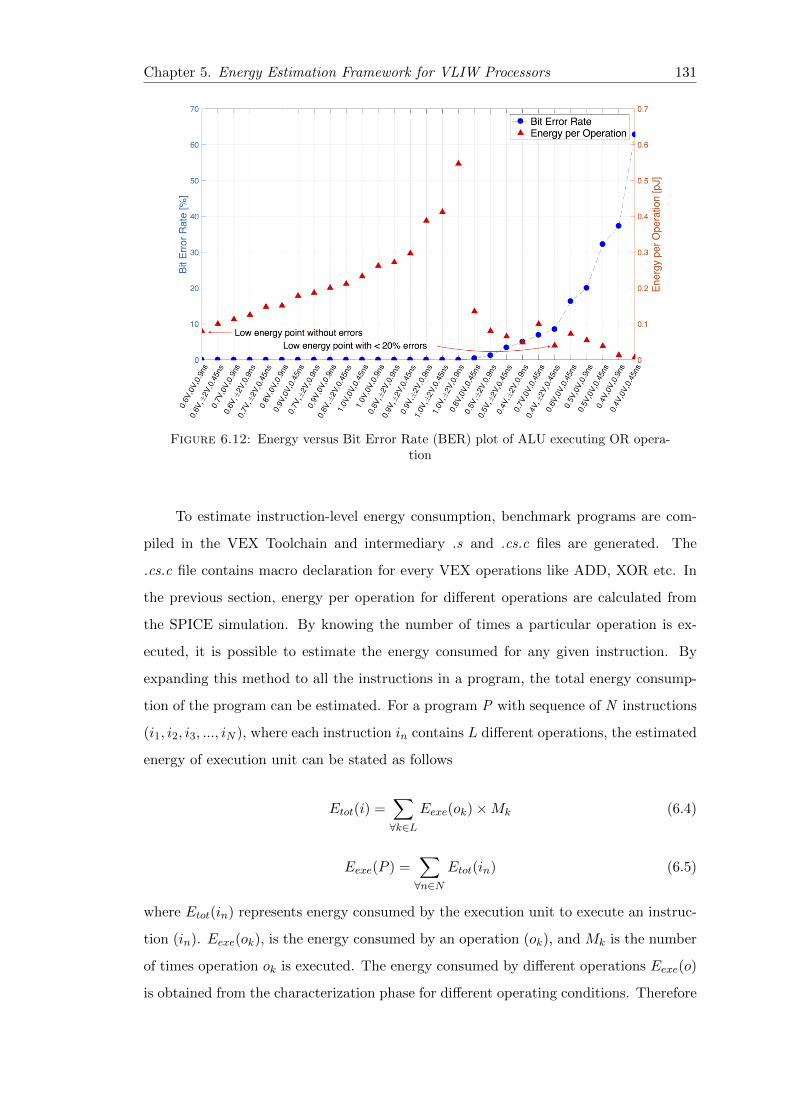
Chapter 5. Energy Estimation Framework for VLIW Processors 131
Figure 6.12: Energy versus Bit Error Rate (BER) plot of ALU executing OR opera-tion
To estimate instruction-level energy consumption, benchmark programs are com-
piled in the VEX Toolchain and intermediary .s and .cs.c files are generated. The
.cs.c file contains macro declaration for every VEX operations like ADD, XOR etc. In
the previous section, energy per operation for different operations are calculated from
the SPICE simulation. By knowing the number of times a particular operation is ex-
ecuted, it is possible to estimate the energy consumed for any given instruction. By
expanding this method to all the instructions in a program, the total energy consump-
tion of the program can be estimated. For a program P with sequence of N instructions
(i1, i2, i3, ..., iN ), where each instruction in contains L different operations, the estimated
energy of execution unit can be stated as follows
Etot(i) =∑∀k∈L
Eexe(ok)×Mk (6.4)
Eexe(P ) =∑∀n∈N
Etot(in) (6.5)
where Etot(in) represents energy consumed by the execution unit to execute an instruc-
tion (in). Eexe(ok), is the energy consumed by an operation (ok), and Mk is the number
of times operation ok is executed. The energy consumed by different operations Eexe(o)
is obtained from the characterization phase for different operating conditions. Therefore

Chapter 5. Energy Estimation Framework for VLIW Processors 132
Figure 6.13: Energy versus Bit Error Rate (BER) plot of ALU executing XOR oper-ation
Figure 6.14: ρ − V EX cluster blocks (highlighted) characterized of for energy esti-mation
Eqn. 6.4 represents the total energy consumed by the execution unit for a particular in-
struction in. Eqn. 6.5 represents the total energy consumption of the execution unit to
execute a program P with N different instructions. Since the focus of this work is only
the execution unit of the ρ− V EX cluster, only the energy consumed by the execution
unit is estimated. Considering arbitrary energy consumption for other modules, total
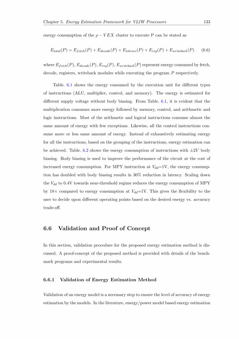
Chapter 5. Energy Estimation Framework for VLIW Processors 133
energy consumption of the ρ− V EX cluster to execute P can be stated as
Etotal(P ) = Efetch(P ) + Edecode(P ) + Etotexec(P ) + Ereg(P ) + Ewriteback(P ) (6.6)
where Efetch(P ), Edecode(P ), Ereg(P ), Ewriteback(P ) represent energy consumed by fetch,
decode, registers, writeback modules while executing the program P respectively.
Table. 6.1 shows the energy consumed by the execution unit for different types
of instructions (ALU, multiplier, control, and memory). The energy is estimated for
different supply voltage without body biasing. From Table. 6.1, it is evident that the
multiplication consumes more energy followed by memory, control, and arithmetic and
logic instructions. Most of the arithmetic and logical instructions consume almost the
same amount of energy with few exceptions. Likewise, all the control instructions con-
sume more or less same amount of energy. Instead of exhaustively estimating energy
for all the instructions, based on the grouping of the instructions, energy estimation can
be achieved. Table. 6.2 shows the energy consumption of instructions with ±2V body
biasing. Body biasing is used to improve the performance of the circuit at the cost of
increased energy consumption. For MPY instruction at Vdd=1V, the energy consump-
tion has doubled with body biasing results in 30% reduction in latency. Scaling down
the Vdd to 0.4V towards near-threshold regime reduces the energy consumption of MPY
by 18× compared to energy consumption at Vdd=1V. This gives the flexibility to the
user to decide upon different operating points based on the desired energy vs. accuracy
trade-off.
6.6 Validation and Proof of Concept
In this section, validation procedure for the proposed energy estimation method is dis-
cussed. A proof-concept of the proposed method is provided with details of the bench-
mark programs and experimental results.
6.6.1 Validation of Energy Estimation Method
Validation of an energy model is a necessary step to ensure the level of accuracy of energy
estimation by the models. In the literature, energy/power model based energy estimation

Chapter 5. Energy Estimation Framework for VLIW Processors 134
Table 6.1: Energy consumption of different VLIW instructions
InstructionsEnergy consumption in pJ (Vbb=0V)
Vdd=1V Vdd=0.8V Vdd=0.7V Vdd=0.6V Vdd=0.5V Vdd=0.4V
sxtb 0.293 0.175 0.144 0.108 0.07 0.0145
cmp 0.276 0.163 0.124 0.09 0.057 0.0139
slct 0.29 0.169 0.132 0.098 0.063 0.0142
mov 0.292 0.172 0.138 0.105 0.065 0.0142
shr 0.29 0.169 0.132 0.098 0.063 0.0142
min 0.267 0.153 0.118 0.082 0.055 0.0137
orc 0.259 0.149 0.11 0.078 0.054 0.0136
xor 0.266 0.153 0.112 0.08 0.055 0.0136
add 0.264 0.152 0.112 0.08 0.055 0.0136
sub 0.261 0.151 0.111 0.79 0.054 0.0152
and 0.261 0.15 0.111 0.79 0.054 0.0136
mpy 0.296 0.196 0.154 0.12 0.077 0.0163
br 0.271 0.158 0.12 0.084 0.055 0.0137
goto 0.282 0.165 0.128 0.094 0.061 0.014
return 0.276 0.163 0.124 0.090 0.058 0.0139
xnop 0.276 0.163 0.124 0.090 0.057 0.0139
ldb 0.292 0.172 0.138 0.106 0.068 0.0143
is validated against gate-level simulation on the set of benchmarks to determine the
accuracy of the models. In [78], RTL macro-model of a VLIW core, register file, and
cache are validated against transistor-level simulation of the circuit. In the proposed
energy estimation method, the execution unit of the ρ−V EX cluster is characterized at
transistor-level for different operating triads. Energy estimation is done by C compiler
at higher abstraction level based on the data from transistor-level characterization and
the user-defined operating conditions. Since the proposed estimation method is based on
transistor-level characterization, to validate this method hardware prototype is required
to perform real-time experiments. Due to unavailability of hardware prototype, we
devise an alternate validation procedure for the proposed energy estimation method.
In this work, the energy estimation done at higher abstraction level is validated by
comparing with the energy estimates at the transistor-level simulation for the selected
benchmarks. Transistor-level simulations provide most accurate energy estimates by
simulating the benchmark program at SPICE level. In this work, an entire ρ − V EX
cluster is synthesized using 28nm FDSOI technology and SPICE simulation of the bench-
mark programs are performed using ELDO SPICE. The energy estimation of the bench-
mark program from the proposed method is compared with full SPICE simulation to

Chapter 5. Energy Estimation Framework for VLIW Processors 135
Table 6.2: Energy consumption of different VLIW instructions with body bias
InstructionsEnergy consumption in pJ (Vbb=±2V )
Vdd=1V Vdd=0.8V Vdd=0.7V Vdd=0.6V Vdd=0.5V Vdd=0.4V
sxtb 0.582 0.295 0.214 0.13 0.0835 0.0514
cmp 0.569 0.28 0.198 0.1285 0.082 0.0504
slct 0.575 0.287 0.208 0.1293 0.0828 0.0509
mov 0.58 0.293 0.21 0.1298 0.0831 0.0513
shr 0.575 0.288 0.208 0.1295 0.0828 0.0509
min 0.56 0.276 0.194 0.1276 0.0815 0.0496
orc 0.544 0.2696 0.1855 0.1242 0.08 0.048
xor 0.559 0.2768 0.1904 0.1272 0.0802 0.0492
add 0.551 0.2736 0.1883 0.126 0.0815 0.0492
sub 0.549 0.272 0.1869 0.1254 0.0805 0.0488
and 0.552 0.2728 0.1876 0.1254 0.0805 0.0484
mpy 0.599 0.31 0.225 0.141 0.085 0.0523
br 0.564 0.278 0.196 0.128 0.0818 0.0498
goto 0.573 0.285 0.205 0.129 0.0825 0.0507
return 0.57 0.28 0.198 0.1285 0.082 0.0504
xnop 0.57 0.28 0.198 0.1285 0.082 0.0504
ldb 0.58 0.293 0.21 0.1298 0.0831 0.0514
determine the accuracy of the proposed method.
The validation is performed for test cases of different ALU operations with different
addressing modes listed as following.
• In the scenario 1, the same operation is repeated multiple times in the same
addressing mode.
• In the scenario 2, different addressing modes of the same operation are executed
in sequence to estimate the difference in energy consumption due to varying ad-
dressing modes while the functionality is same.
• In the scenario 3, different operations with different addressing modes are used.
SPICE simulation of benchmark program on ρ− V EX cluster takes a substantial
amount of time and computing resources. In order to simplify the validation process, test
program with different arithmetic and logical operations is created inline with the above
listed test scenarios. In order to further simplify the validation process, some modules of
the VLIW cluster are executed at C level. The test program is compiled and assembled
by the VEX C compiler. The output ASM code is translated to series of opcode signals

Chapter 5. Energy Estimation Framework for VLIW Processors 136
in SPICE format by a translator script developed in this work. The translated opcode
signals are fed to the execution unit of ρ − V EX cluster for transistor-level simulation
with random inputs. This method gives the accurate energy consumption of the test
program next to real time hardware implementation. The energy consumption data
from the transistor-level simulation are compared with the data of the energy estimation
method proposed in this work.
Figure 6.15: Flow graph of validation method
In scenario 1, register-direct and immediate addressing modes are used for different
arithmetic and logical operations. The test program with the sequence of instructions is
simulated using ELDO SPICE. From this experiment, we observed no big difference in
the energy consumption of any of the arithmetic and logical operations while repeating
in the same addressing mode. In scenario 2, all the arithmetic and logical operations in
immediate addressing mode consume slightly more energy compared to register-direct
addressing mode. Scenario 3 is used to study the inter-instruction effects while exe-
cuting different operations. For the energy estimation methods, where the base energy
is computed as NOP and incremental energy is augmented with base energy to esti-
mate energy consumption for different operations. In such models, inter-instruction
effects have to be compensated by arbitrary offset value or by separate models for inter-
instruction energy proposed in [81]. In this work, we propose energy estimation on
functional-level by studying the impact of different instructions on different modules of
the ρ− V EX cluster. Therefore, inter-instruction effects are inherently handled in the

Chapter 5. Energy Estimation Framework for VLIW Processors 137
proposed method, which voids the need for additional offset to improve the accuracy of
the estimated energy.
Table 6.3: Validation of proposed energy estimation method
Test scenario Average Error Maximum Error
Scenario 1 (immediate addressing mode) 0.23% 1.13%
Scenario 1 (register-direct addressing mode) 0.19% 0.89%
Scenario 2 0.22% 1.36%
Scenario 3 2% 2.34%
Table 6.3 shows the validation results of the proposed energy estimation method
against transistor-level simulation of benchmarks. The test program for different test
scenarios is simulated at SPICE level as shown in Fig. 6.15. Similarly, proposed en-
ergy estimation method is used to estimate energy for all the test scenarios of the test
program. Finally both the results are compared to validate the accuracy of the pro-
posed energy estimation method. Average error and maximum error are the two figure
of merits used to determine the accuracy of the proposed method. In scenario 1 for
different arithmetic and logical operations with immediate addressing mode, there is an
average error of 0.23% in the proposed method compared to transistor-level simulation.
Likewise, for register-direct addressing mode, the average error is 0.19%. In both the
cases, the average error is negligible and the maximum error is also within the acceptable
margin. In scenario 2, where an operation is executed repeatedly in different addressing
modes, the average error is 0.22% and the maximum error is 1.36%. Scenario 3 records
highest average error of 2% and the maximum error of 2.34%. In the validation proce-
dure, execution stage of ρ − V EX cluster along with other modules are simulated at
transistor-level. This provides more accurate energy estimation at the cost of enormous
simulation time. The error in the proposed method is due to estimation at high-level
C compilation based on transistor-level characterization of functional units. The aim
of this work is to estimate energy consumption by simple C compilation which is many
times faster compared to transistor-level simulations. Because of the transistor-level
characterization of functional units, the average error in energy estimation is within the
acceptable limits. In the proposed energy estimation method benchmark programs can
be compiled and energy can be estimated in few minutes compared to hours of SPICE
simulation based energy estimation.
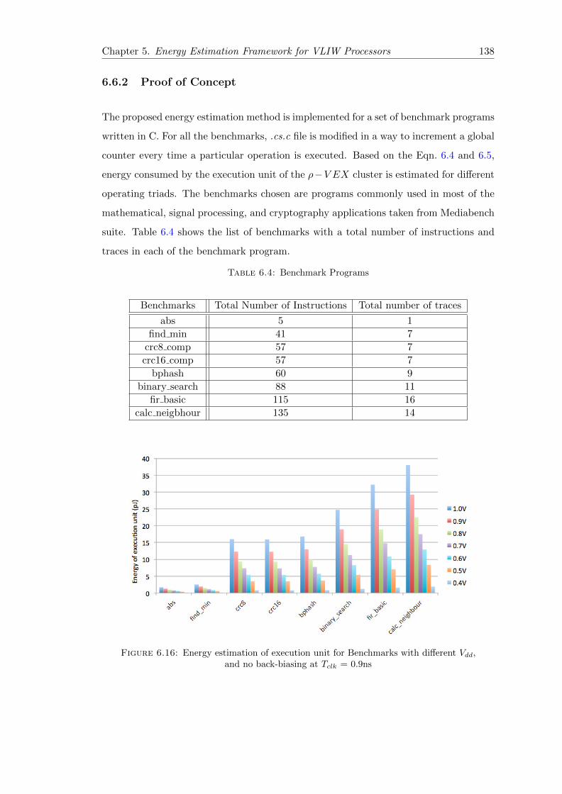
Chapter 5. Energy Estimation Framework for VLIW Processors 138
6.6.2 Proof of Concept
The proposed energy estimation method is implemented for a set of benchmark programs
written in C. For all the benchmarks, .cs.c file is modified in a way to increment a global
counter every time a particular operation is executed. Based on the Eqn. 6.4 and 6.5,
energy consumed by the execution unit of the ρ−V EX cluster is estimated for different
operating triads. The benchmarks chosen are programs commonly used in most of the
mathematical, signal processing, and cryptography applications taken from Mediabench
suite. Table 6.4 shows the list of benchmarks with a total number of instructions and
traces in each of the benchmark program.
Table 6.4: Benchmark Programs
Benchmarks Total Number of Instructions Total number of traces
abs 5 1
find min 41 7
crc8 comp 57 7
crc16 comp 57 7
bphash 60 9
binary search 88 11
fir basic 115 16
calc neigbhour 135 14
Figure 6.16: Energy estimation of execution unit for Benchmarks with different Vdd,and no back-biasing at Tclk = 0.9ns

Chapter 5. Energy Estimation Framework for VLIW Processors 139
Figure 6.17: Energy estimation of execution unit for Benchmarks with different Vdd,with back-biasing Vbb = 2V, and Tclk = 0.9ns
The modified .cs.c is executed using a C compiler to estimate the energy consump-
tion for different operation triads. Fig. 6.16 shows the energy estimation of the execution
unit of ρ−V EX cluster for benchmark programs under different Vdd ranging from 1V to
0.4V without back-biasing. Reducing Vdd from 1V to 0.4V reduces the energy consump-
tion of execution unit by 20 × on average for all the benchmarks. But the significant
energy gains are limited by the timing errors as shown in energy versus BER plots in the
characterization section. This limitation can be overcome by applying body-biasing to
limit BER to an acceptable margin at the cost of reduced energy gains. Fig. 6.17 shows
the energy estimation of benchmarks with body-biasing Vbb = 2V. With body-bias, at
Vdd =0.4V, energy consumption reduces by 11 × on average for all the benchmarks.
In addition to voltage over-scaling, overclocking is employed by reducing the clock
period Tclk from 0.9ns to 0.45ns. This improves the energy gains at the cost of increased
BER. At reduced clock period, benchmark programs achieve 31 × reduction in energy
consumption at 0.4V compared to 1V. With body-biasing of Vbb = 2V, timing errors are
limited and the energy consumption is reduced by 10 × on average compared to energy
consumption at 1V. The proposed framework provides an easy way to understand the
behaviour of the execution unit of ρ− V EX cluster for different operating triads. With
the proposed framework, the user can decide the optimum trade-off between energy
versus accuracy for any given program by choosing most suitable operating triads at
runtime.
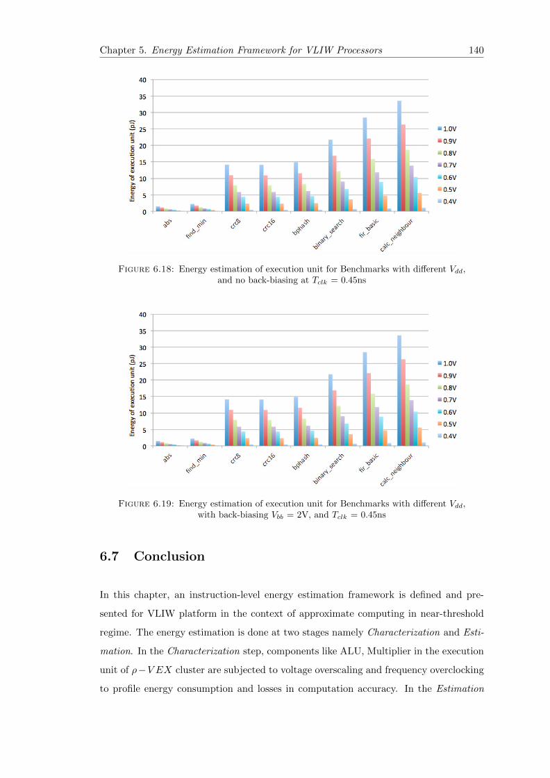
Chapter 5. Energy Estimation Framework for VLIW Processors 140
Figure 6.18: Energy estimation of execution unit for Benchmarks with different Vdd,and no back-biasing at Tclk = 0.45ns
Figure 6.19: Energy estimation of execution unit for Benchmarks with different Vdd,with back-biasing Vbb = 2V, and Tclk = 0.45ns
6.7 Conclusion
In this chapter, an instruction-level energy estimation framework is defined and pre-
sented for VLIW platform in the context of approximate computing in near-threshold
regime. The energy estimation is done at two stages namely Characterization and Esti-
mation. In the Characterization step, components like ALU, Multiplier in the execution
unit of ρ−V EX cluster are subjected to voltage overscaling and frequency overclocking
to profile energy consumption and losses in computation accuracy. In the Estimation

Chapter 5. Energy Estimation Framework for VLIW Processors 141
step, based on the characterization profile, energy consumption of execution unit can
be easily estimated for any given program by simple C compilation process using VEX
Toolchain. A validation procedure is developed to estimate the accuracy of the pro-
posed energy estimation framework. In this work, instruction-level energy consumption
is estimated for 8 benchmark programs. The proposed framework estimation is 98%
accurate when compared to full SPICE simulation of the benchmark program. The ben-
efit of using body-biasing technique is highlighted to reduce error rate at near-threshold
regime at the cost of reduced energy gains. The proposed energy estimation framework
is simple, very fast, and accurate in estimating the energy consumption for different
operating conditions. In this work, scope for energy estimation is limited to execution
of ρ − V EX cluster, this can be further expanded to other modules like fetch, decode,
and writeback in the cluster.


Chapter 7
Conclusion and Perspectives
7.1 Overview
In this thesis, a framework is proposed to handle timing errors and to estimate energy
consumption of error resilient applications in the scope of near-threshold computing. In
the energy crunching environment, keeping the device functional for the long haul is the
major challenge in the present trend of digital design. Various low-power techniques
are explored at different levels of abstraction to improve the energy efficiency. Dynamic
voltage scaling is a prominent low-power technique used to increase the energy efficiency
of the designs by reducing the supply voltage at runtime. In this work, we have explored
near-threshold computing to enhance the energy gains by scaling down the supply volt-
age close to the threshold voltage of the transistor. Reducing the supply voltage makes
the design more vulnerable to variability effects and timing errors. We have proposed
to use FDSOI, an inherent low-leakage technology to counter the variability effects by
effective body-biasing technique. Different error handling techniques like double sam-
pling methods are conventionally used to tackle errors. Most of the double sampling
techniques use fixed speculation window to detect and correct the timing errors. In this
work, we have proposed dynamic speculation window-based error detection and correc-
tion method to handle the timing errors while scaling the supply voltage close to the
threshold voltage. We have demonstrated the advantage of dynamic speculation method
in Xilinx FPGA platform along with conventional double sampling method. We over-
clocked the benchmark programs in FPGA beyond the estimated maximum frequency to
invoke timing errors in the design. Also, variability effects are introduced in the design
143
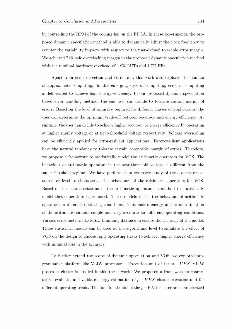
Chapter 6. Conclusion and Perspectives 144
by controlling the RPM of the cooling fan on the FPGA. In these experiments, the pro-
posed dynamic speculation method is able to dynamically adjust the clock frequency to
counter the variability impacts with respect to the user-defined tolerable error margin.
We achieved 71% safe overclocking margin in the proposed dynamic speculation method
with the minimal hardware overhead of 1.9% LUTs and 1.7% FFs.
Apart from error detection and correction, this work also explores the domain
of approximate computing. In this emerging style of computing, error in computing
is deliberated to achieve high energy efficiency. In our proposed dynamic speculation
based error handling method, the end user can decide to tolerate certain margin of
errors. Based on the level of accuracy required for different classes of applications, the
user can determine the optimum trade-off between accuracy and energy efficiency. At
runtime, the user can decide to achieve higher accuracy or energy efficiency by operating
at higher supply voltage or at near-threshold voltage respectively. Voltage overscaling
can be efficiently applied for error-resilient applications. Error-resilient applications
have the natural tendency to tolerate certain acceptable margin of errors. Therefore,
we propose a framework to statistically model the arithmetic operators for VOS. The
behaviour of arithmetic operators in the near-threshold voltage is different from the
super-threshold regime. We have performed an extensive study of these operators at
transistor level to characterize the behaviours of the arithmetic operators for VOS.
Based on the characterization of the arithmetic operators, a method to statistically
model these operators is proposed. These models reflect the behaviour of arithmetic
operators in different operating conditions. This makes energy and error estimation
of the arithmetic circuits simple and very accurate for different operating conditions.
Various error metrics like MSE, Hamming distance to ensure the accuracy of the model.
These statistical models can be used at the algorithmic level to simulate the effect of
VOS on the design to choose right operating triads to achiever higher energy efficiency
with minimal loss in the accuracy.
To further extend the scope of dynamic speculation and VOS, we explored pro-
grammable platform like VLIW processors. Execution unit of the ρ − V EX VLIW
processor cluster is studied in this thesis work. We proposed a framework to charac-
terize, evaluate, and validate energy estimation of ρ − V EX cluster execution unit for
different operating triads. The functional units of the ρ−V EX cluster are characterized
Chapter 6. Conclusion and Perspectives 145
at transistor level to extract accurate energy and error data for different operating tri-
ads. Transistor-level simulations are very slow even for the simpler program. Therefore,
we proposed an instruction-level energy estimation method by a simple compilation of
C program. By this, we can estimate the energy of a program for different operating
conditions very quickly from accurate transistor-level characterization. We also pro-
posed an alternate validation procedure to ensure the accuracy of the proposed energy
estimation method by comparing with full SPICE simulation of the benchmarks. In this
framework, we achieved very accurate energy estimation with an average error of less
than 2%.
7.2 Unified Approach
An important challenge in digital circuit design is to achieve high energy efficiency at
minimal cost in terms of silicon footprint and acceptable compromise in accuracy or
performance of the circuit. Due to the quadratic dependence of energy consumption on
the supply voltage, reducing Vdd yields higher energy efficiency. A simple observation of
different CMOS technology in the past decade shows the trend of voltage scaling. In near-
threshold region, delay and energy are roughly linear with Vdd. Operating transistors
in the near-threshold regime offer better control over energy-error trade-off. FDSOI
technology is used to improve the benefits of near-threshold computing. But the impact
of variability and timing errors outweighs the benefits of near-threshold computing. In
this thesis, we addressed this problem by three contributions.
Fig. 7.1 shows an overall perspective of this thesis. Fig. 7.1 shows a VLIW cluster
with different pipeline stages like instruction fetch, decode, execution stage represented
by functional units (FU), register files and memory blocks. In a typical execution flow,
instructions are fetched and decoded by instruction fetch and decode stage. Different
operations in each of the instructions are executed by different FUs in parallel. The
outputs are recorded in the register files and memory. To achieve high energy efficiency,
voltage scaling can be applied to FUs. Reduction in Vdd results in timing errors that
can be handled using various methods explained in Chapter 3. In Chapter 3, limitations
of the existing methods are discussed in detail. Also, the need for a unified approach to
handle errors is insisted to achieve best energy-error trade-off.
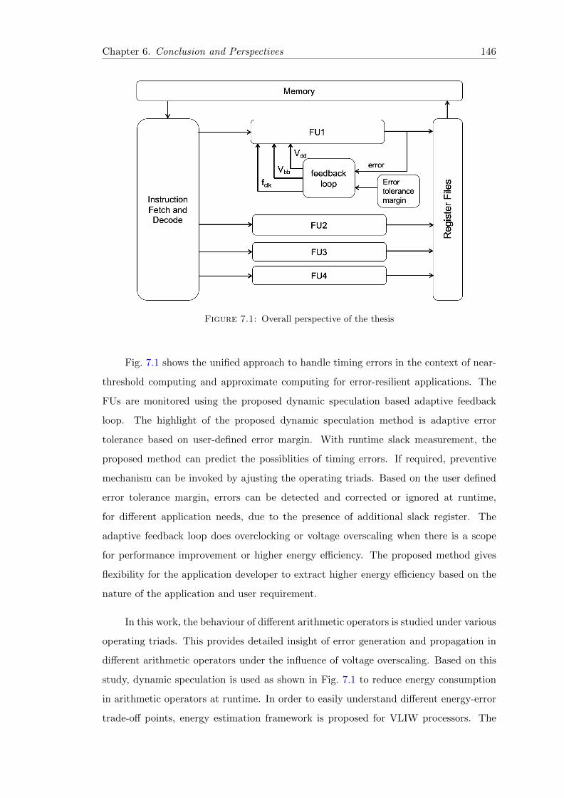
Chapter 6. Conclusion and Perspectives 146
Figure 7.1: Overall perspective of the thesis
Fig. 7.1 shows the unified approach to handle timing errors in the context of near-
threshold computing and approximate computing for error-resilient applications. The
FUs are monitored using the proposed dynamic speculation based adaptive feedback
loop. The highlight of the proposed dynamic speculation method is adaptive error
tolerance based on user-defined error margin. With runtime slack measurement, the
proposed method can predict the possiblities of timing errors. If required, preventive
mechanism can be invoked by ajusting the operating triads. Based on the user defined
error tolerance margin, errors can be detected and corrected or ignored at runtime,
for different application needs, due to the presence of additional slack register. The
adaptive feedback loop does overclocking or voltage overscaling when there is a scope
for performance improvement or higher energy efficiency. The proposed method gives
flexibility for the application developer to extract higher energy efficiency based on the
nature of the application and user requirement.
In this work, the behaviour of different arithmetic operators is studied under various
operating triads. This provides detailed insight of error generation and propagation in
different arithmetic operators under the influence of voltage overscaling. Based on this
study, dynamic speculation is used as shown in Fig. 7.1 to reduce energy consumption
in arithmetic operators at runtime. In order to easily understand different energy-error
trade-off points, energy estimation framework is proposed for VLIW processors. The
Chapter 6. Conclusion and Perspectives 147
proposed energy estimation framework simulates any given benchmark program using
C compiler and provides energy estimation for different operating triads. This helps
the application developer to understand the benefits and costs to achieve best possible
energy-error trade-off.
7.3 Future Work
7.3.1 Improvements in Dynamic Speculation Window Method
Some of the high end, off-the-shelf commercial FPGAs support voltage scaling. Dynamic
speculation window-based error handling method can be experimented with voltage
overscaling in FPGA platform to further enhance the feedback loop. By this, it is more
realistic to demonstrate the advantages of dynamic speculation to counter the variability
effects by adjusting both voltage and frequency at runtime.
7.3.2 Improving VOS of Approximate Operators
In this work, adders and multipliers are studied at near-threshold regime to create the
statistical model to mimic the behaviour of these operators. A proof of concept is shown
in this work by modelling different adder configurations. Similar to adders, some study
is done for multipliers by utilizing adder models in the final stage of parallel prefix
multiplier. This can be further extended by studying the tree structure used in these
multipliers to generate partial products. Likewise, other arithmetic operators can also
be modelled to create a library of VOS operators. By this, it will be very easy to simulate
the trade-off given by approximate computing for any complex design. In this work, a
near-threshold logic library is designed by sizing the transistors to achieve higher energy
gains. The statistical model can be linked to the near-threshold logic library to improve
the accuracy of the model.
7.3.3 Improving Energy Estimation of ρ− V EX Cluster
In this work, only the execution unit of the ρ−V EX cluster is characterized to estimate
the energy. The proposed framework can be further improved by modelling the entire

Chapter 6. Conclusion and Perspectives 148
cluster using SPICE simulations. Already some of the other modules like decoder, etc.
are simulated at SPICE level. Once the whole cluster is modelled, there is a lot of scope
to dynamically change the processor configuration by altering the issue width and other
parameters. Since the functional units are same, the existing framework can estimate
the energy for different configurations at runtime.

Publications
[1] RahulKumar Bhudhwani, Rengarajan Ragavan, and Olivier Sentieys. Taking advan-
tage of correlation in stochastic computing. In IEEE Proc. of the Intl. Symp. on
Circuits and Systems (ISCAS), pages 1–4, 2017.
[2] Rengarajan Ragavan, Benjamin Barrois, Cedric Killian, and Olivier Sentieys. Push-
ing the limits of voltage over-scaling for error-resilient applications. In IEEE/ACM
Proc. Conf. of the Design Automation & Test in Europe (DATE), pages 476–481,
2017.
[3] Rengarajan Ragavan, Cedric Killian, and Olivier Sentieys. Low complexity on-chip
distributed DC-DC converter for low power WSN nodes. In IEEE New Circuits and
Systems Conference (NEWCAS), pages 1–4, 2015.
[4] Rengarajan Ragavan, Cedric Killian, and Olivier Sentieys. Adaptive overclocking
and error correction based on dynamic speculation window. In IEEE Computer
Society Annual Symp. on VLSI (ISVLSI), pages 325–330, 2016.
149
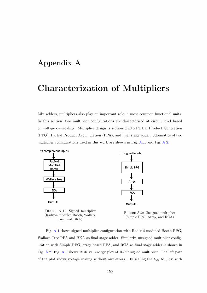
Appendix A
Characterization of Multipliers
Like adders, multipliers also play an important role in most common functional units.
In this section, two multiplier configurations are characterized at circuit level based
on voltage overscaling. Multiplier design is sectioned into Partial Product Generation
(PPG), Partial Product Accumulation (PPA), and final stage adder. Schematics of two
multiplier configurations used in this work are shown in Fig. A.1, and Fig. A.2.
Figure A.1: Signed multiplier(Radix-4 modified Booth, Wallace
Tree, and BKA)
Figure A.2: Unsigned multiplier(Simple PPG, Array, and RCA)
Fig. A.1 shows signed multiplier configuration with Radix-4 modified Booth PPG,
Wallace Tree PPA and BKA as final stage adder. Similarly, unsigned multiplier config-
uration with Simple PPG, array based PPA, and RCA as final stage adder is shown in
Fig. A.2. Fig. A.3 shows BER vs. energy plot of 16-bit signed multiplier. The left part
of the plot shows voltage scaling without any errors. By scaling the Vdd to 0.6V with
150
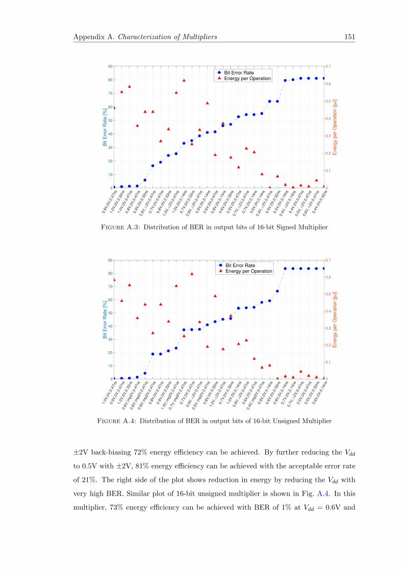
Appendix A. Characterization of Multipliers 151
0.9
V,0
V,0
.47ns
1.0
V,0
V,0
.32ns
1.0
V,0
V,0
.47ns
0.8
V,0
V,0
.47ns
0.9
V,0
V,0
.32ns
0.9
V,
2V
,0.4
7ns
0.7
V,0
V,0
.47ns
0.8
V,0
V,0
.32ns
1.0
V,
2V
,0.4
7ns
1.0
V,0
V,0
.14ns
0.7
V,0
V,0
.32ns
0.8
V,
2V
,0.4
7ns
0.9
V,0
V,0
.14ns
0.6
V,0
V,0
.47ns
0.8
V,0
V,0
.14ns
0.6
V,0
V,0
.32ns
0.5
V,0
V,0
.47ns
0.7
V,
2V
,0.4
7ns
0.7
V,0
V,0
.14ns
0.6
V,0
V,0
.14ns
0.4
V,
2V
,0.4
7ns
0.5
V,0
V,0
.32ns
0.5
V,0
V,0
.14ns
0.4
V,
2V
,0.1
4ns
0.4
V,0
V,0
.47ns
0.5
V,
2V
,0.4
7ns
0.6
V,
2V
,0.4
7ns
0.4
V,0
V,0
.32ns
0
10
20
30
40
50
60
70
80
90
Bit E
rro
r R
ate
[%
]
0
0.1
0.2
0.3
0.4
0.5
0.6
0.7
En
erg
y p
er
Op
era
tio
n [
pJ]
Bit Error RateEnergy per Operation
Figure A.3: Distribution of BER in output bits of 16-bit Signed Multiplier
1.0
V,0
V,0
.47ns
0.9
V,0
V,0
.47ns
1.0
V,0
V,0
.32ns
0.6
V,\m
p2V
,0.4
7ns
0.8
V,\m
p2V
,0.4
7ns
0.9
V,\m
p2V
,0.4
7ns
0.8
V,0
V,0
.47ns
0.9
V,0
V,0
.32ns
1.0
V,\m
p2V
,0.4
7ns
0.7
V,\m
p2V
,0.4
7ns
0.7
V,0
V,0
.47ns
0.9
V,
2V
,0.4
7ns
0.5
V,\m
p2V
,0.4
7ns
0.8
V,0
V,0
.32ns
1.0
V,
2V
,0.4
7ns
0.7
V,0
V,0
.32ns
1.0
V,0
V,0
.14ns
0.8
V,
2V
,0.4
7ns
0.6
V,0
V,0
.47ns
0.4
V,\m
p2V
,0.4
7ns
0.9
V,0
V,0
.14ns
0.6
V,0
V,0
.32ns
0.8
V,0
V,0
.14ns
0.7
V,0
V,0
.14ns
0.7
V,
2V
,0.4
7ns
0.5
V,0
V,0
.47ns
0.5
V,0
V,0
.32ns
0.6
V,0
V,0
.14ns
0
10
20
30
40
50
60
70
80
90
Bit E
rro
r R
ate
[%
]
0
0.1
0.2
0.3
0.4
0.5
0.6
0.7
En
erg
y p
er
Op
era
tio
n [
pJ]
Bit Error RateEnergy per Operation
Figure A.4: Distribution of BER in output bits of 16-bit Unsigned Multiplier
±2V back-biasing 72% energy efficiency can be achieved. By further reducing the Vdd
to 0.5V with ±2V, 81% energy efficiency can be achieved with the acceptable error rate
of 21%. The right side of the plot shows reduction in energy by reducing the Vdd with
very high BER. Similar plot of 16-bit unsigned multiplier is shown in Fig. A.4. In this
multiplier, 73% energy efficiency can be achieved with BER of 1% at Vdd = 0.6V and

Appendix A. Characterization of Multipliers 152
Vbb = ±2V. The efficiency can be further improved to 82% with BER of 20% at Vdd =
0.5V and Vbb = ±2V.
As shown in Chapter 5, like adders, multipliers can also be statistically modelled
for VOS. These parallel prefix multipliers use Brent-Kung and Ripple Carry adder in
their final stage. This gives the advantage of using same BKA and RCA VOS models
in this stage. The partial product generation and partial product accumulation stages
have to be modelled to obtain the full model of the multipliers. This is one of the future
work of this thesis.


Bibliography
[1] Tadahiro Kuroda and Kojiro Suzuki. Variable supply-voltage scheme for low-power
high-speed CMOS digital design. IEEE Journal of Solid-State Circuits, 33(3):454–
462, 1998.
[2] Etienne Le Sueur and Gernot Heiser. Dynamic voltage and frequency scaling: The
laws of diminishing returns. In Proc. of the 2010 Intl. Conf. on Power Aware
Computing and Systems, pages 1–8, 2010.
[3] Edward Stott, Zhenyu Guan, Joshua M Levine, Justin SJ Wong, and Peter YK
Cheung. Variation and reliability in FPGAs. IEEE Design & Test, 30(6):50–59,
2013.
[4] Michael Nicolaidis. Double-sampling design paradigm—a compendium of architec-
tures. IEEE Trans. on Device and Materials Reliability, 15(1):10–23, 2015.
[5] Edward Stott, Joshua M Levine, Peter YK Cheung, and Nachiket Kapre. Timing
fault detection in fpga-based circuits. In IEEE 22nd Annual International Sympo-
sium on Field-Programmable Custom Computing Machines (FCCM), pages 96–99.
IEEE, 2014.
[6] Alexander Brant, Ahmed Abdelhadi, Douglas HH Sim, Shao Lin Tang, Michael Xi
Yue, and Guy GF Lemieux. Safe overclocking of tightly coupled CGRAs and pro-
cessor arrays using razor. In IEEE 21st Annual International Symposium on Field-
Programmable Custom Computing Machines (FCCM), pages 37–44. IEEE, 2013.
[7] Joshua M Levine, Edward Stott, George Constantinides, and Peter YK Cheung.
Online measurement of timing in circuits: For health monitoring and dynamic
voltage & frequency scaling. In IEEE 20th Annual International Symposium on
154

Bibliography 155
Field-Programmable Custom Computing Machines (FCCM), pages 109–116. IEEE,
2012.
[8] Joseph A Fisher, Paolo Faraboschi, and Cliff Young. Embedded computing: a VLIW
approach to architecture, compilers and tools. Elsevier, 2005.
[9] Gordon E. Moore. Cramming more components onto integrated circuits. Electron-
ics, 38(8):114–117, 1965.
[10] ITRS. International Technology Roadmap for Semiconductors 2007 ed. Executive
Summary. Technical report, ITRS, 2011.
[11] Nor Zaidi Haron and Said Hamdioui. Why is CMOS scaling coming to an end? In
International Design and Test Workshop, pages 98–103, 2008.
[12] ITRS. International Technology Roadmap for Semiconductors 2011 ed. Design.
Technical report, ITRS, 2011.
[13] Martin Wirnshofer. Sources of variation. In Variation Aware Adaptive Voltage
Scaling For Digital CMOS Circuits, Springer series in advanced microelectronics ,
Vol 41, chapter 2. Springer, 2013. ISBN 9789400761964.
[14] Jui-Ming Chang and Massoud Pedram. Low power design. In Power optimiza-
tion and synthesis at behavioral and system levels using formal methods, chapter 1.
Springer Science & Business Media, 2012.
[15] Ali Dasdan and Ivan Hom. Handling inverted temperature dependence in static
timing analysis. ACM Transactions on Design Automation of Electronic Systems
(TODAES), 11(2):306–324, 2006.
[16] D Suleiman, M Ibrahim, and I Hamarash. Dynamic voltage frequency scaling
(DVFS) for microprocessors power and energy reduction. In International Confer-
ence on Electrical and Electronics Engineering, 2005.
[17] Intel. Enhanced Intel R© speedstep R© technology for the intel R© pentium R© M pro-
cessor. Technical report, Intel, 2004.
[18] AMD. AMD powernow technology. Technical report, AMD, 2000.
[19] Ivan Miro-Panades, Edith Beigne, Yvain Thonnart, Laurent Alacoque, Pascal
Vivet, Suzanne Lesecq, Diego Puschini, Anca Molnos, Farhat Thabet, and Benoit

Bibliography 156
Tain. A fine-grain variation-aware dynamic vdd-hopping AVFS architecture on a
32 nm GALS MPSoC. IEEE Journal of Solid-State Circuits, 49(7):1475–1486, 2014.
[20] Robin Wilson, Edith Beigne, Philippe Flatresse, Alexandre Valentian, Fady
Abouzeid, Thomas Benoist, Christian Bernard, Sebastien Bernard, Olivier Billoint,
and Sylvain Clerc. A 460MHz at 397mV, 2.6 GHz at 1.3 V, 32b VLIW DSP, em-
bedding fmax tracking. In IEEE Intl. Solid-State Circuits Conf. Digest of Technical
Papers (ISSCC), pages 452–453. IEEE, 2014.
[21] Davide Rossi, Antonio Pullini, Igor Loi, Michael Gautschi, Frank Kagan Gurkaynak,
Adam Teman, Jeremy Constantin, Andreas Burg, Ivan Miro-Panades, and Edith
Beigne. 193 MOPS/mW@ 162 MOPS, 0.32 V to 1.15 V voltage range multi-core
accelerator for energy efficient parallel and sequential digital processing. In IEEE
Symposium in Low-Power and High-Speed Chips (COOL CHIPS XIX), pages 1–3.
Ieee, 2016.
[22] Ronald G Dreslinski, Michael Wieckowski, David Blaauw, Dennis Sylvester, and
Trevor Mudge. Near-threshold computing: Reclaiming moore’s law through energy
efficient integrated circuits. Proceedings of the IEEE, 98(2):253–266, 2010.
[23] Benton H. Calhoun and David Brooks. Can subthreshold and near-threshold circuits
go mainstream? IEEE Micro, 30(4):80–85, 2010.
[24] Ulya R Karpuzcu, Krishna B Kolluru, Nam Sung Kim, and Josep Torrellas.
VARIUS-NTV: A microarchitectural model to capture the increased sensitivity of
manycores to process variations at near-threshold voltages. In IEEE/IFIP Interna-
tional Conference on Dependable Systems and Networks (DSN), pages 1–11. IEEE,
2012.
[25] David Blaauw and Bo Zhai. Energy efficient design for subthreshold supply voltage
operation. In IEEE Proceedings of the International Symposium on Circuits and
Systems (ISCAS), pages 4–pp, 2006.
[26] K Cheng, A Khakifirooz, P Kulkarni, S Ponoth, J Kuss, D Shahrjerdi, LF Edge,
A Kimball, S Kanakasabapathy, and K Xiu. Extremely thin SOI (ETSOI) CMOS
with record low variability for low power system-on-chip applications. In IEEE
International Electron Devices Meeting (IEDM), pages 1–4, 2009.
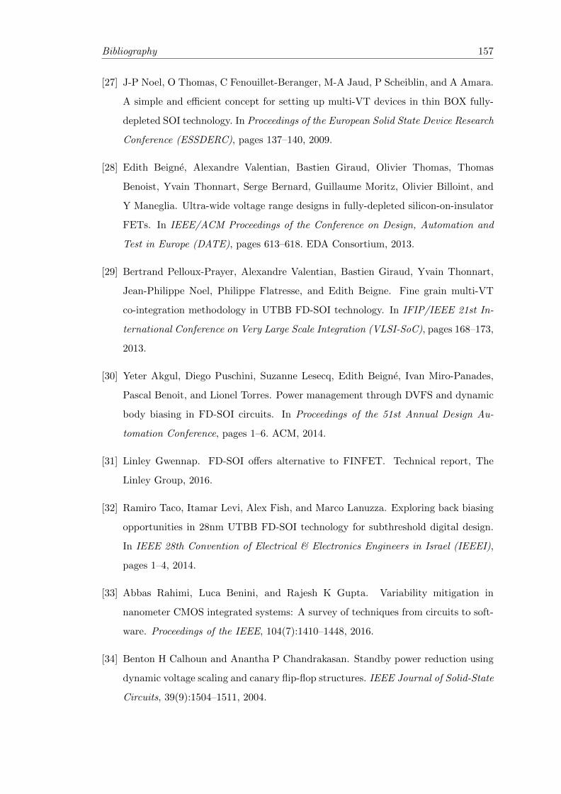
Bibliography 157
[27] J-P Noel, O Thomas, C Fenouillet-Beranger, M-A Jaud, P Scheiblin, and A Amara.
A simple and efficient concept for setting up multi-VT devices in thin BOX fully-
depleted SOI technology. In Proceedings of the European Solid State Device Research
Conference (ESSDERC), pages 137–140, 2009.
[28] Edith Beigne, Alexandre Valentian, Bastien Giraud, Olivier Thomas, Thomas
Benoist, Yvain Thonnart, Serge Bernard, Guillaume Moritz, Olivier Billoint, and
Y Maneglia. Ultra-wide voltage range designs in fully-depleted silicon-on-insulator
FETs. In IEEE/ACM Proceedings of the Conference on Design, Automation and
Test in Europe (DATE), pages 613–618. EDA Consortium, 2013.
[29] Bertrand Pelloux-Prayer, Alexandre Valentian, Bastien Giraud, Yvain Thonnart,
Jean-Philippe Noel, Philippe Flatresse, and Edith Beigne. Fine grain multi-VT
co-integration methodology in UTBB FD-SOI technology. In IFIP/IEEE 21st In-
ternational Conference on Very Large Scale Integration (VLSI-SoC), pages 168–173,
2013.
[30] Yeter Akgul, Diego Puschini, Suzanne Lesecq, Edith Beigne, Ivan Miro-Panades,
Pascal Benoit, and Lionel Torres. Power management through DVFS and dynamic
body biasing in FD-SOI circuits. In Proceedings of the 51st Annual Design Au-
tomation Conference, pages 1–6. ACM, 2014.
[31] Linley Gwennap. FD-SOI offers alternative to FINFET. Technical report, The
Linley Group, 2016.
[32] Ramiro Taco, Itamar Levi, Alex Fish, and Marco Lanuzza. Exploring back biasing
opportunities in 28nm UTBB FD-SOI technology for subthreshold digital design.
In IEEE 28th Convention of Electrical & Electronics Engineers in Israel (IEEEI),
pages 1–4, 2014.
[33] Abbas Rahimi, Luca Benini, and Rajesh K Gupta. Variability mitigation in
nanometer CMOS integrated systems: A survey of techniques from circuits to soft-
ware. Proceedings of the IEEE, 104(7):1410–1448, 2016.
[34] Benton H Calhoun and Anantha P Chandrakasan. Standby power reduction using
dynamic voltage scaling and canary flip-flop structures. IEEE Journal of Solid-State
Circuits, 39(9):1504–1511, 2004.
Bibliography 158
[35] Dan Ernst, Shidhartha Das, Seokwoo Lee, David Blaauw, Todd Austin, Trevor
Mudge, Nam Sung Kim, and Krisztian Flautner. Razor: circuit-level correction of
timing errors for low-power operation. IEEE Micro, 2004.
[36] Yuji Kunitake, Toshinori Sato, Hiroto Yasuura, and Takanori Hayashida. Possibili-
ties to miss predicting timing errors in canary flip-flops. In IEEE 54th Intl. Midwest
Symp. on Circuits and Systems (MWSCAS), pages 1–4, 2011.
[37] Shidhartha Das, Carlos Tokunaga, Sanjay Pant, Wei-Hsiang Ma, Sudherssen Kalai-
selvan, Kevin Lai, David M Bull, and David T Blaauw. RazorII: In situ error de-
tection and correction for PVT and SER tolerance. IEEE Journal of Solid-State
Circuits, 44(1):32–48, 2009.
[38] Matthew Fojtik, David Fick, Yejoong Kim, Nathaniel Pinckney, David Money Har-
ris, David Blaauw, and Dennis Sylvester. Bubble razor: Eliminating timing margins
in an ARM Cortex-M3 processor in 45 nm cmos using architecturally independent
error detection and correction. IEEE Journal of Solid-State Circuits, 48(1):66–81,
2013.
[39] Michael Nicolaidis. GRAAL: a new fault tolerant design paradigm for mitigating
the flaws of deep nanometric technologies. In IEEE International Test Conference
(ITC), pages 1–10. IEEE, 2007.
[40] Robert Baumann. Soft errors in advanced computer systems. IEEE Design & Test
of Computers, 22(3):258–266, 2005.
[41] Thomas Schweizer, Anja Kuster, Sven Eisenhardt, Tommy Kuhn, and Wolfgang
Rosenstiel. Using run-time reconfiguration to implement fault-tolerant coarse
grained reconfigurable architectures. In IEEE 26th International Parallel and Dis-
tributed Processing Symposium Workshops (IPDPSW), pages 320–327, 2012.
[42] Thomas Schweizer, Philipp Schlicker, Sven Eisenhardt, Tommy Kuhn, and Wolf-
gang Rosenstiel. Low-cost TMR for fault-tolerance on coarse-grained reconfigurable
architectures. In International Conference on Reconfigurable Computing and FP-
GAs (ReConFig), pages 135–140, 2011.
[43] Thomas Schweizer, Wolfgang Rosenstiel, Luigi Vaz Ferreira, and Marcus Ritt. Tim-
ing error handling on CGRAs. In International Conference on Reconfigurable Com-
puting and FPGAs (ReConFig), pages 1–6, 2013.
Bibliography 159
[44] Subhasish Mitra, Nirmal R Saxena, and Edward J McCluskey. A design diversity
metric and analysis of redundant systems. IEEE Transactions on Computers, 51
(5):498–510, 2002.
[45] Pedro Reviriego, Chris J Bleakley, and Juan Antonio Maestro. Diverse double
modular redundancy: A new direction for soft-error detection and correction. IEEE
Design & Test, 30(2):87–95, 2013.
[46] Pedro Reviriego, Chris J Bleakley, and Juan Antonio Maestro. Structural DMR:
A technique for implementation of soft-error-tolerant fir filters. IEEE Transactions
on Circuits and Systems II: Express Briefs, 58(8):512–516, 2011.
[47] Jaeyoon Kim and Sandip Tiwari. Inexact computing for ultra low-power nanome-
ter digital circuit design. In IEEE/ACM International Symposium on Nanoscale
Architectures, pages 24–31, 2011.
[48] Michael Schaffner, Frank K Gurkaynak, Aljosa Smolic, Hubert Kaeslin, and
Luca Benini. An approximate computing technique for reducing the complex-
ity of a direct-solver for sparse linear systems in real-time video processing. In
ACM/EDAC/IEEE Design Automation Conference (DAC), pages 1–6, 2014.
[49] Jie Han and Michael Orshansky. Approximate computing: An emerging paradigm
for energy-efficient design. In IEEE European Test Symposium (ETS), pages 1–6,
2013.
[50] G Tziantzioulis and AM Gok. Lazy pipelines: Enhancing quality in approximate
computing. In Proc. Conf. of the Design Automation & Test in Europe, pages
1381–1386, 2016.
[51] Amir Yazdanbakhsh, Divya Mahajan, and Bradley Thwaites. Axilog: Language
support for approximate hardware design. In Proc. Conf. of the Design Automation
& Test in Europe (DATE), pages 812–817, 2015.
[52] Michael Nicolaidis. Time redundancy based soft-error tolerance to rescue nanometer
technologies. In IEEE Proc. of the VLSI Test Symp., pages 86–94, 1999.
[53] Joshua M Levine, Edward Stott, George Constantinides, and Peter YK Cheung.
SMI: Slack measurement insertion for online timing monitoring in FPGAs. In Proc.
Int. Conf. on Field Programmable Logic and Applications (FPL), pages 1–4, 2013.

Bibliography 160
[54] Justin SJ Wong, Pete Sedcole, and Peter YK Cheung. Self-measurement of combi-
natorial circuit delays in FPGAs. ACM Trans. on Reconfigurable Technology and
Systems (TRETS), 2(2):10, 2009.
[55] Pete Sedcole, Justin S Wong, and Peter YK Cheung. Characterisation of FPGA
clock variability. In IEEE Computer Society Annual Symp. on VLSI (ISVLSI),
pages 322–328, 2008.
[56] Xilinx. VC707 Evaluation Board for the Virtex-7 FPGA User Guide, v1.6 edition,
April 2015.
[57] A Benhassain, F Cacho, V Huard, S Mhira, L Anghel, C Parthasarathy, A Jain,
and A Sivadasan. Robustness of timing in-situ monitors for AVS management. In
IEEE International Reliability Physics Symposium (IRPS), pages CR–4, 2016.
[58] A Benhassain, S Mhira, F Cacho, V Huard, and L Anghel. In-situ slack monitors:
taking up the challenge of on-die monitoring of variability and reliability. In IEEE
International Verification and Security Workshop (IVSW), pages 1–5. IEEE, 2016.
[59] LB Soares and Sergio Bampi. Near-threshold computing for very wide frequency
scaling: Approximate adders to rescue performance. In IEEE New Circuits and
Systems Conference (NEWCAS), pages 1–4, 2015.
[60] Younghoon Kim, Swagath Venkataramani, Kaushik Roy, and Anand Raghunathan.
Designing approximate circuits using clock overgating. In Proc. of the 53rd Annual
Design Automation Conference, page 15, 2016.
[61] Ismail Akturk, Nam Sung Kim, and Ulya R Karpuzcu. Decoupled control and data
processing for approximate near-threshold voltage computing. IEEE Micro, 35(4):
70–78, 2015.
[62] Chaofan Li, Wei Luo, Sachin S Sapatnekar, and Jiang Hu. Joint precision opti-
mization and high level synthesis for approximate computing. In Proc. of the 52nd
Annual Design Automation Conference, page 104, 2015.
[63] Avinash Lingamneni and Christian Enz. Energy parsimonious circuit design
through probabilistic pruning. In Proc. Conf. of the Design Automation & Test
in Europe (DATE), pages 1–6, 2011.
Bibliography 161
[64] Jeremy Schlachter, Vincent Camus, and Christian Enz. Near/sub-threshold circuits
and approximate computing: The perfect combination for ultra-low-power systems.
In IEEE Computer Society Annual Symp. on VLSI, pages 476–480, 2015.
[65] Avinash Lingamneni, Christian Enz, Krishna Palem, and Christian Piguet. Design-
ing energy-efficient arithmetic operators using inexact computing. Journal of Low
Power Electronics, 9(1):141–153, 2013.
[66] Weste Neil HE. CMOS VLSI Design: A Circuits And Systems Perspective, 4/E.
Pearson Education India, 2006.
[67] Andrew B Kahng and Seokhyeong Kang. Accuracy-configurable adder for approx-
imate arithmetic designs. In Proc. of the Annual Design Automation Conference,
pages 820–825, 2012.
[68] Rengarajan Ragavan, Cedric Killian, and Olivier Sentieys. Adaptive overclocking
and error correction based on dynamic speculation window. In IEEE Computer
Society Annual Symp. on VLSI (ISVLSI), pages 325–330, 2016.
[69] Stephan Wong, Thijs Van As, and Geoffrey Brown. ρ-VEX: A reconfigurable and
extensible softcore VLIW processor. In International Conference on Electrical and
Computer Engineering (ICECE), pages 369–372, 2008.
[70] Anthony Brandon and Stephan Wong. Support for dynamic issue width in VLIW
processors using generic binaries. In Proc. Conf. of the Design Automation & Test
in Europe (DATE), pages 827–832, 2013.
[71] Alireza Dehghani, Aubrey Dunne, David Moloney, and Oscar Deniz. Application
processor description. Technical report, Movidius, 2016.
[72] Thijs Van As. ρ-VEX: A reconfigurable and extensible softcore VLIW processor.
Technical report, Delft University of Technology, 2008.
[73] Hewlet-Packard Laboratories. VEX toolchain. Technical report, HP, 2011.
[74] Chaitali Chakrabarti and Dinesh Gaitonde. Instruction level power model of micro-
controllers. In IEEE Proceedings of the International Symposium on Circuits and
Systems (ISCAS), volume 1, pages 76–79, 1999.
Bibliography 162
[75] Vivek Tiwari, Sharad Malik, Andrew Wolfe, and Mike Tien-Chien Lee. Instruction
level power analysis and optimization of software. In Technologies for Wireless
Computing, pages 139–154. Springer, 1996.
[76] Huzefa Mehta, Robert Michael Owens, and Mary Jane Irwin. Instruction level
power profiling. In IEEE Proceedings of the International Conference on Acoustics,
Speech, and Signal Processing (ICASSP), volume 6, pages 3326–3329, 1996.
[77] Vittorio Zaccaria, Mariagiovanna Sami, Donatella Sciuto, and Cristina Silvano.
Power estimation and optimization methodologies for VLIW-based embedded sys-
tems. Springer Science & Business Media, 2007. ISBN 1402073771.
[78] Luca Benini, Davide Bruni, Mauro Chinosi, Christina Silvano, Vittorio Zaccaria,
and Roberto Zafalon. A power modeling and estimation framework for vliw-based
embedded systems. In Proc. Intl. Workshop on Power And Timing Modeling, Op-
timization and Simulation PATMOS, volume 1, pages 2–3, 2001.
[79] David M Brooks, Pradip Bose, Stanley E Schuster, Hans Jacobson, Prabhakar N
Kudva, Alper Buyuktosunoglu, J Wellman, Victor Zyuban, Manish Gupta, and
Peter W Cook. Power-aware microarchitecture: Design and modeling challenges
for next-generation microprocessors. IEEE Micro, 20(6):26–44, 2000.
[80] Erkan Diken, Rosilde Corvino, and Lech Jozwiak. Rapid and accurate energy
estimation of vector processing in vliw asips. In Mediterranean Conference on
Embedded Computing (MECO), pages 33–37, 2013.
[81] Sourav Roy, Rajat Bhatia, and Ashish Mathur. An accurate energy estimation
framework for VLIW processor cores. In International Conference on Computer
Design (ICCD), pages 464–469. IEEE, 2007.
[82] Andrea Bona, Mariagiovanna Sami, Donatella Sciuto, Vittorio Zaccaria, Cristina
Silvano, and Roberto Zafalon. Energy estimation and optimization of embedded
VLIW processors based on instruction clustering. In Proceedings of the annual
Design Automation Conference, pages 886–891. ACM, 2002.
[83] Michael Meixner and Tobias G Noll. Limits of gate-level power estimation consider-
ing real delay effects and glitches. In International Symposium on System-on-Chip
(SoC), pages 1–7. IEEE, 2014.


