Erik Jonsson School of Engineering and Th U i it f T t D ...
Erik Jonsson School of Engineering and Th U i it f T t D ll g gComputer ScienceThe University of Texas at Dallas
Take-Home ExerciseTake-Home Exercise
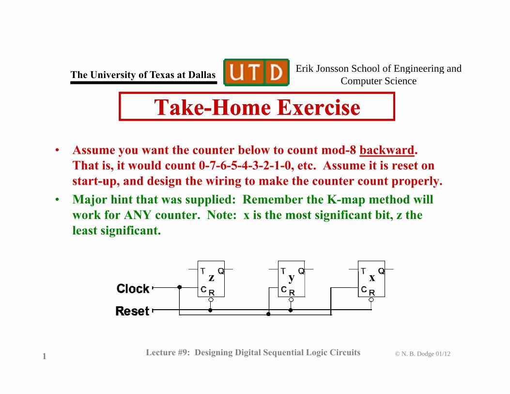
• Assume you want the counter below to count mod-8 backward. That is, it would count 0-7-6-5-4-3-2-1-0, etc. Assume it is reset on start-up, and design the wiring to make the counter count properly.
• Major hint that was supplied: Remember the K-map method will work for ANY counter. Note: x is the most significant bit, z the least significant.
z y x
© N. B. Dodge 01/12Lecture #9: Designing Digital Sequential Logic Circuits1
Erik Jonsson School of Engineering and Th U i it f T t D ll g gComputer ScienceThe University of Texas at Dallas
Exercise 1Exercise 1
Clock
Reset
y x
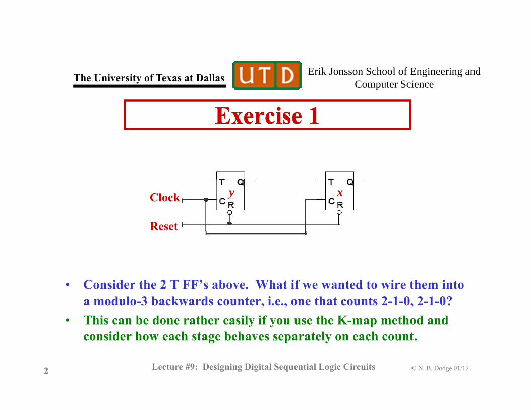
C id th 2 T FF’ b Wh t if t d t i th i t• Consider the 2 T FF’s above. What if we wanted to wire them into a modulo-3 backwards counter, i.e., one that counts 2-1-0, 2-1-0?
• This can be done rather easily if you use the K-map method and consider how each stage behaves separately on each count
© N. B. Dodge 01/12Lecture #9: Designing Digital Sequential Logic Circuits2
consider how each stage behaves separately on each count.
Erik Jonsson School of Engineering and Th U i it f T t D ll g gComputer ScienceThe University of Texas at Dallas
Designing Sequential LogicDesigning Sequential Logic
• Last lecture demonstrated the design of two simple counters (a third counter was asimple counters (a third counter was a homework problem).
• Today’s exercise: Three additional designs:Today s exercise: Three additional designs: – A timer or signal generator– A “sequential” multiplexerq p– A modulo-10 binary counter
• Note that all the designs utilize counters.
© N. B. Dodge 01/12Lecture #9: Designing Digital Sequential Logic Circuits3
Erik Jonsson School of Engineering and Th U i it f T t D ll g gComputer ScienceThe University of Texas at Dallas
A Signal GeneratorA Signal Generator• The desired design is a signal generator based on a counter. • Specification:
4 bit bi h ( ll l) t d i b 50/50 l k– 4-bit binary synchronous (parallel) counter, driven by a 50/50 clock. – Counter runs continually, reset only at startup by a “Reset-” signal. – Since 24 = 16, counter counts modulo-16.
C t t “ i l ” t 3 7 d 14 hi h– Counter generates “sync signals” on counts 3, 7, and 14, which: • Occur immediately after the counts are valid (i.e., immediately
after the counter output stages change). • Occur for 1/2 clock cycle only• Occur for 1/2 clock cycle only.
• Per “spec,” we need a 4-bit counter. We can use the standard T FF that we used to build the 3-bit counter in the last lesson. We
ill d f f th
© N. B. Dodge 01/12Lecture #9: Designing Digital Sequential Logic Circuits4
will need four of these.
Erik Jonsson School of Engineering and Th U i it f T t D ll g gComputer ScienceThe University of Texas at Dallas
Designing the TimerDesigning the Timer
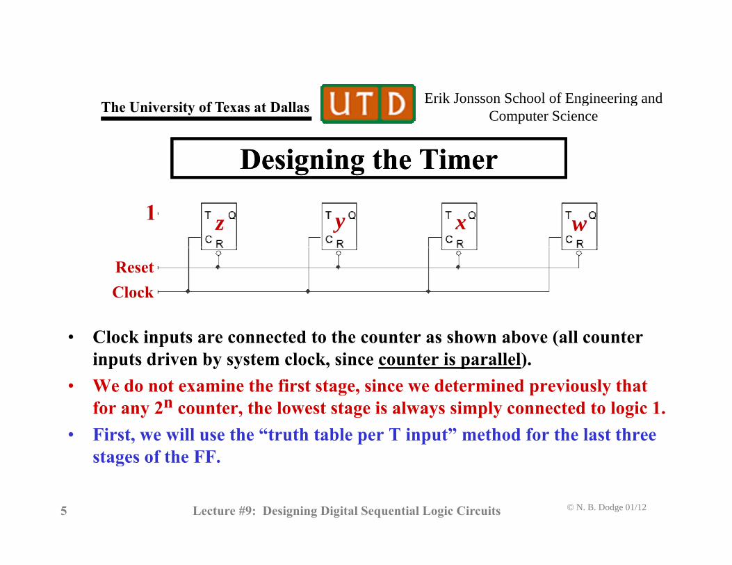
y x w1 z
ClockReset
• Clock inputs are connected to the counter as shown above (all counter inputs driven by system clock, since counter is parallel).
• We do not examine the first stage, since we determined previously thatWe do not examine the first stage, since we determined previously that for any 2n counter, the lowest stage is always simply connected to logic 1.
• First, we will use the “truth table per T input” method for the last three stages of the FF.
© N. B. Dodge 01/12Lecture #9: Designing Digital Sequential Logic Circuits5
stages of the FF.
Erik Jonsson School of Engineering and Th U i it f T t D ll g gComputer ScienceThe University of Texas at Dallas
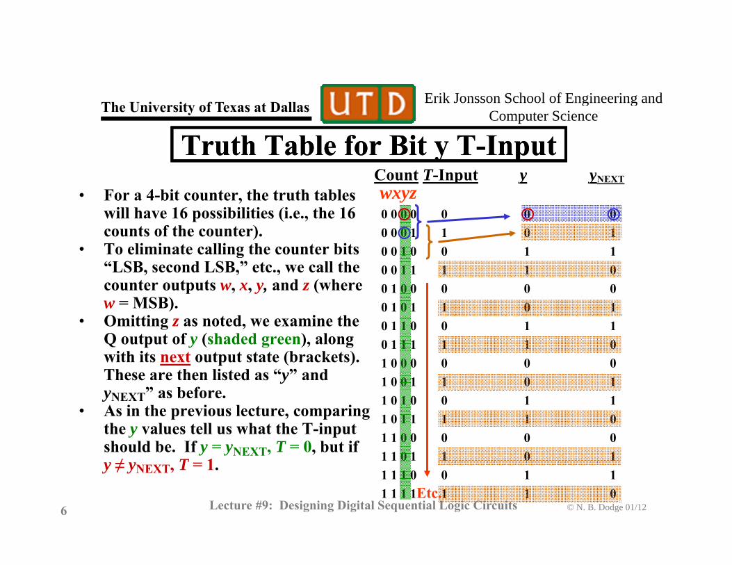
Count T-Input y yNEXT
Truth Table for Bit y T-InputTruth Table for Bit y T-InputCount T-Input y yNEXT
0 0 0 0 0 0 00 0 0 1 1 0 10 0 1 0 0 1 1
• For a 4-bit counter, the truth tables will have 16 possibilities (i.e., the 16 counts of the counter).
• To eliminate calling the counter bits
wxyz
0 0 1 0 0 1 10 0 1 1 1 1 00 1 0 0 0 0 00 1 0 1 1 0 1
• To eliminate calling the counter bits “LSB, second LSB,” etc., we call the counter outputs w, x, y, and z (where w = MSB). O itti t d i th 0 1 1 0 0 1 1
0 1 1 1 1 1 01 0 0 0 0 0 01 0 0 1 1 0 1
• Omitting z as noted, we examine the Q output of y (shaded green), along with its next output state (brackets). These are then listed as “y” and
” b f 1 0 1 0 0 1 11 0 1 1 1 1 01 1 0 0 0 0 01 1 0 1 1 0 1
yNEXT” as before. • As in the previous lecture, comparing
the y values tell us what the T-input should be. If y = yNEXT, T = 0, but if≠ T 1
© N. B. Dodge 01/12Lecture #9: Designing Digital Sequential Logic Circuits6
1 1 1 0 0 1 11 1 1 1 1 1 0
y ≠ yNEXT, T = 1.
Etc.
Erik Jonsson School of Engineering and Th U i it f T t D ll g gComputer ScienceThe University of Texas at Dallas
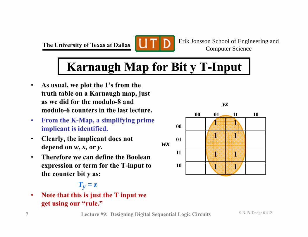
Karnaugh Map for Bit y T-InputKarnaugh Map for Bit y T-Input• As usual, we plot the 1’s from the
truth table on a Karnaugh map, just as we did for the modulo-8 and yzas we did for the modulo 8 and modulo-6 counters in the last lecture.
• From the K-Map, a simplifying prime implicant is identified.
1 1
1 1
yz
00
00 01 11 10
• Clearly, the implicant does not depend on w, x, or y.
• Therefore we can define the Boolean i t f th T i t t
1
1
1 1
wx01
11
expression or term for the T-input to the counter bit y as:
Ty = zN t th t thi i j t th T i t
1 1
10
© N. B. Dodge 01/12Lecture #9: Designing Digital Sequential Logic Circuits7
• Note that this is just the T input we get using our “rule.”
Erik Jonsson School of Engineering and Th U i it f T t D ll g gComputer ScienceThe University of Texas at Dallas
Bit y T Input ConnectedBit y T Input Connected
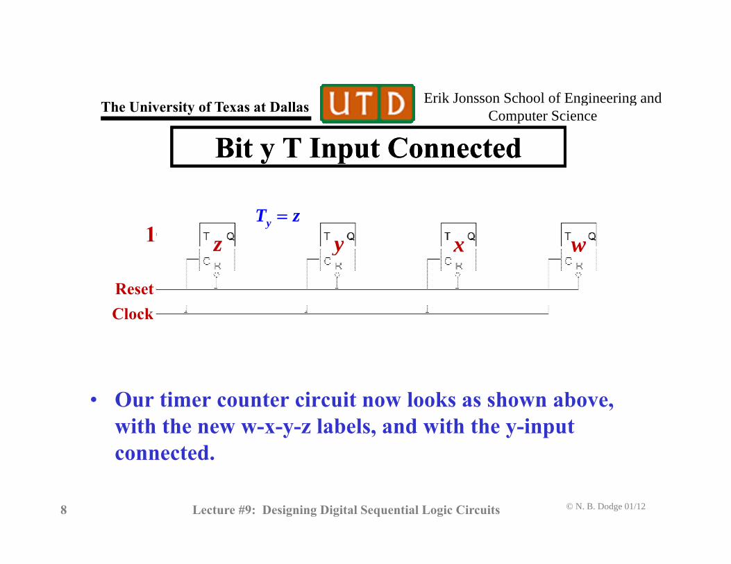
y x w1 zyT z
y x wz
ClockResetClock
• Our timer counter circuit now looks as shown above, with the new w-x-y-z labels, and with the y-input connected.
© N. B. Dodge 01/12Lecture #9: Designing Digital Sequential Logic Circuits8
co ec ed.
Erik Jonsson School of Engineering and Th U i it f T t D ll g gComputer ScienceThe University of Texas at Dallas
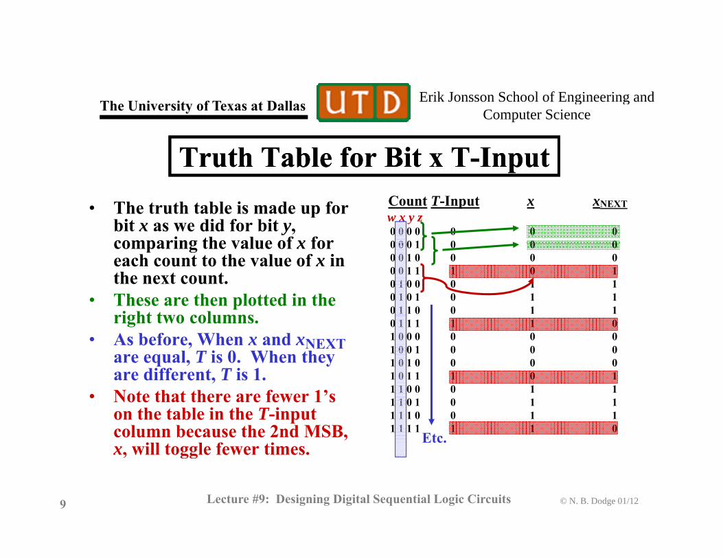
Truth Table for Bit x T-InputTruth Table for Bit x T-Input• The truth table is made up for
bit x as we did for bit y, comparing the value of x for
Count T-Input x xNEXTw x y z0 0 0 0 0 0 00 0 0 1 0 0 0comparing the value of x for
each count to the value of x in the next count.
• These are then plotted in the i ht t l
0 0 0 1 0 0 00 0 1 0 0 0 00 0 1 1 1 0 10 1 0 0 0 1 10 1 0 1 0 1 10 1 1 0 0 1 1right two columns.
• As before, When x and xNEXTare equal, T is 0. When they are different, T is 1.
0 1 1 1 1 1 01 0 0 0 0 0 01 0 0 1 0 0 01 0 1 0 0 0 01 0 1 1 1 0 1
• Note that there are fewer 1’s on the table in the T-input column because the 2nd MSB, x, will toggle fewer times.
1 1 0 0 0 1 11 1 0 1 0 1 11 1 1 0 0 1 11 1 1 1 1 1 0
Etc.
© N. B. Dodge 01/12Lecture #9: Designing Digital Sequential Logic Circuits9
, gg
Erik Jonsson School of Engineering and Th U i it f T t D ll g gComputer ScienceThe University of Texas at Dallas
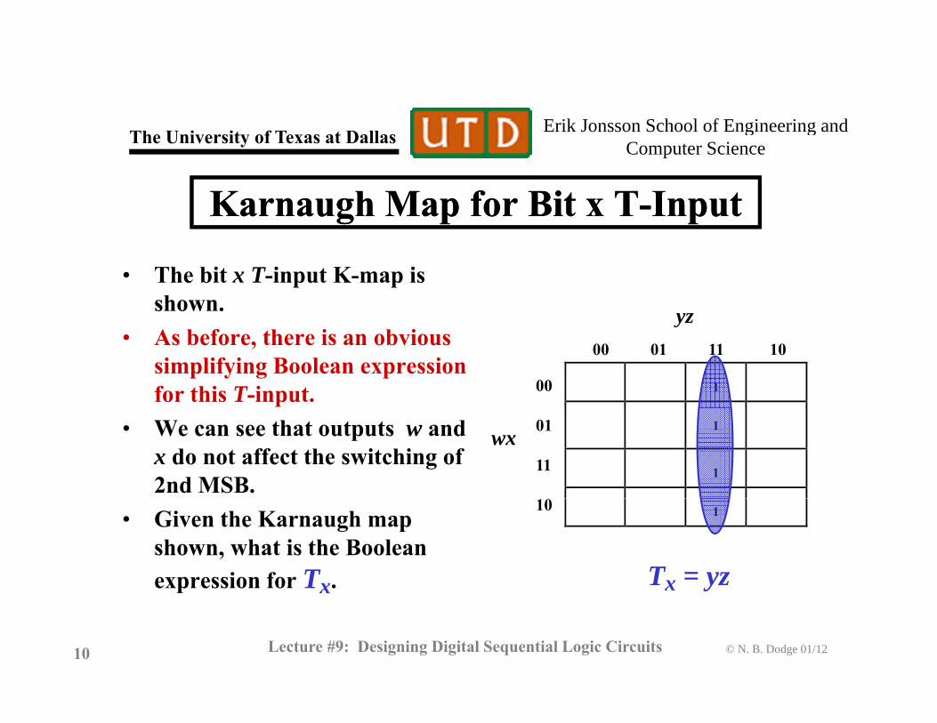
Karnaugh Map for Bit x T-InputKarnaugh Map for Bit x T-Input
• The bit x T-input K-map is shown. yz
1
• As before, there is an obvious simplifying Boolean expression for this T-input.
yz
00
00 01 11 10
1
1
• We can see that outputs w and x do not affect the switching of 2nd MSB.
wx01
11
1
• Given the Karnaugh map
shown, what is the Boolean expression for Tx.
10
Tx = yz
© N. B. Dodge 01/12Lecture #9: Designing Digital Sequential Logic Circuits10
p x x y
Erik Jonsson School of Engineering and Th U i it f T t D ll g gComputer ScienceThe University of Texas at Dallas
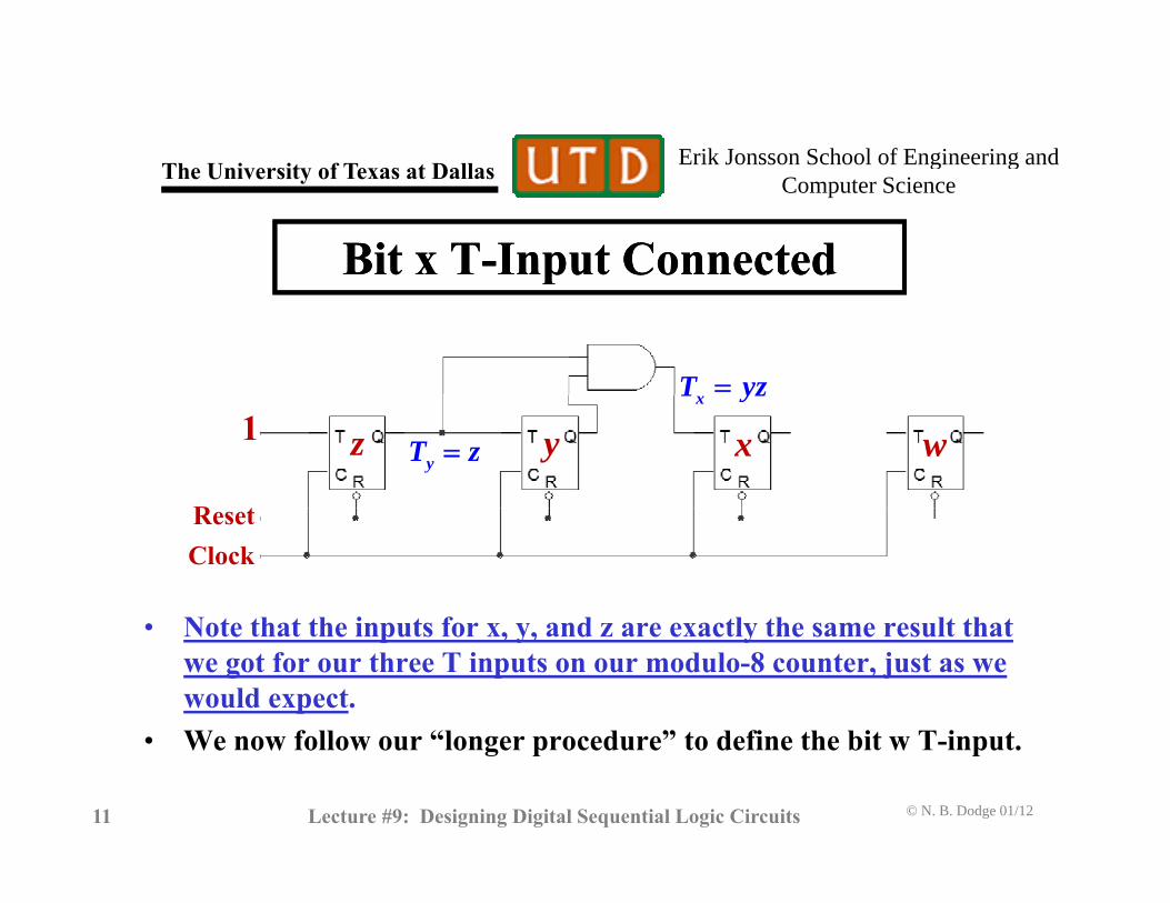
Bit x T-Input ConnectedBit x T-Input Connectedpp
T yz
y x w1 z
R t
yT z
xT yz
N t th t th i t f d tl th lt th t
ClockReset
• Note that the inputs for x, y, and z are exactly the same result that we got for our three T inputs on our modulo-8 counter, just as we would expect. We now follow our “longer procedure” to define the bit w T input
© N. B. Dodge 01/12Lecture #9: Designing Digital Sequential Logic Circuits11
• We now follow our “longer procedure” to define the bit w T-input.
Erik Jonsson School of Engineering and Th U i it f T t D ll g gComputer ScienceThe University of Texas at Dallas
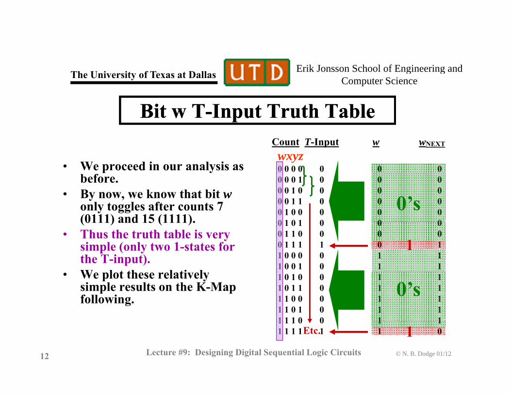
Bit w T-Input Truth TableBit w T-Input Truth Table
• We proceed in our analysis as
Count T-Input w wNEXT
wxyz0 0 0 0 0 0 0p y
before. • By now, we know that bit w
only toggles after counts 7 (0111) and 15 (1111).
0 0 0 1 0 0 00 0 1 0 0 0 00 0 1 1 0 0 00 1 0 0 0 0 00 1 0 1 0 0 0
0’s(0111) and 15 (1111).
• Thus the truth table is very simple (only two 1-states for the T-input). W l t th l ti l
0 1 0 1 0 0 00 1 1 0 0 0 00 1 1 1 1 0 11 0 0 0 0 1 11 0 0 1 0 1 1
1
• We plot these relatively simple results on the K-Map following.
1 0 1 0 0 1 11 0 1 1 0 1 11 1 0 0 0 1 11 1 0 1 0 1 11 1 1 0 0 1 1
0’s
© N. B. Dodge 01/12Lecture #9: Designing Digital Sequential Logic Circuits12
1 1 1 0 0 1 11 1 1 1 1 1 0Etc. 1
Erik Jonsson School of Engineering and Th U i it f T t D ll g gComputer ScienceThe University of Texas at Dallas
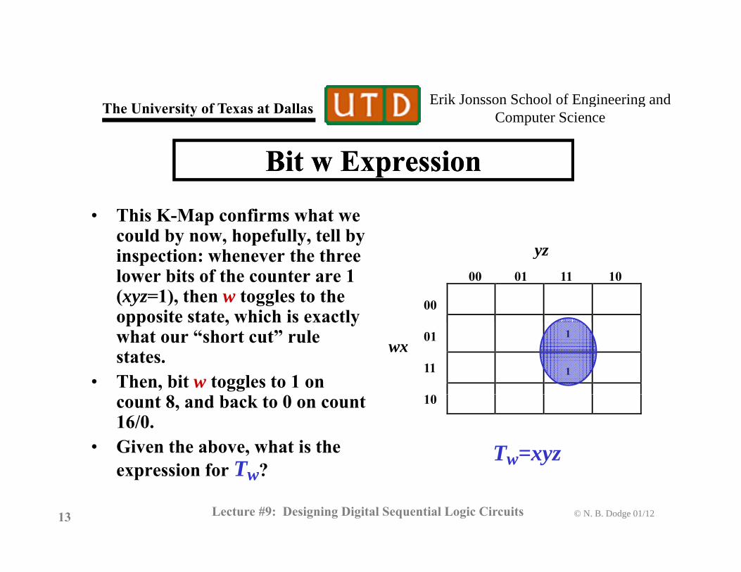
Bit w ExpressionBit w Expression
• This K-Map confirms what we could by now, hopefully, tell by i ti h th th yzinspection: whenever the three lower bits of the counter are 1 (xyz=1), then w toggles to the opposite state, which is exactly
yz
00
00 01 11 10
1
1
opposite state, which is exactly what our “short cut” rule states.
• Then, bit w toggles to 1 on
wx01
11
count 8, and back to 0 on count 16/0.
• Given the above, what is the i f T ?
10
Tw=xyz
© N. B. Dodge 01/12Lecture #9: Designing Digital Sequential Logic Circuits13
expression for Tw?
Erik Jonsson School of Engineering and Th U i it f T t D ll g gComputer ScienceThe University of Texas at Dallas
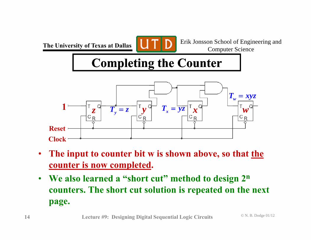
Completing the CounterCompleting the Counter
1wT xyz
y x w1 z
Reset
yT z xT yz
• The input to counter bit w is shown above, so that the counter is now completed
Clock
counter is now completed. • We also learned a “short cut” method to design 2n
counters. The short cut solution is repeated on the next
© N. B. Dodge 01/12Lecture #9: Designing Digital Sequential Logic Circuits14
page.
Erik Jonsson School of Engineering and Th U i it f T t D ll g gComputer ScienceThe University of Texas at Dallas
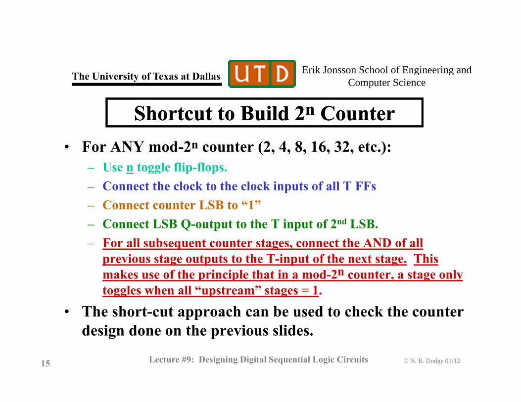
Shortcut to Build 2n CounterShortcut to Build 2n Counter• For ANY mod-2n counter (2, 4, 8, 16, 32, etc.):
– Use n toggle flip-flops.– Connect the clock to the clock inputs of all T FFs – Connect counter LSB to “1”– Connect LSB Q-output to the T input of 2nd LSB.Connect LSB Q output to the T input of 2 LSB.– For all subsequent counter stages, connect the AND of all
previous stage outputs to the T-input of the next stage. This makes use of the principle that in a mod-2n counter, a stage onlymakes use of the principle that in a mod 2 counter, a stage only toggles when all “upstream” stages = 1.
• The short-cut approach can be used to check the counter d i d th i lid
© N. B. Dodge 01/12Lecture #9: Designing Digital Sequential Logic Circuits15
design done on the previous slides.
Erik Jonsson School of Engineering and Th U i it f T t D ll g gComputer ScienceThe University of Texas at Dallas
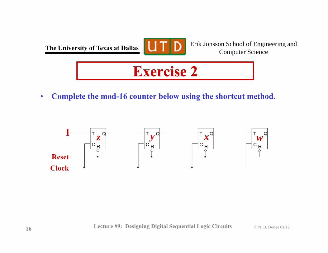
Exercise 2Exercise 2• Complete the mod-16 counter below using the shortcut method.
y x w1 z
ClockReset
© N. B. Dodge 01/12Lecture #9: Designing Digital Sequential Logic Circuits16
Erik Jonsson School of Engineering and Th U i it f T t D ll g gComputer ScienceThe University of Texas at Dallas
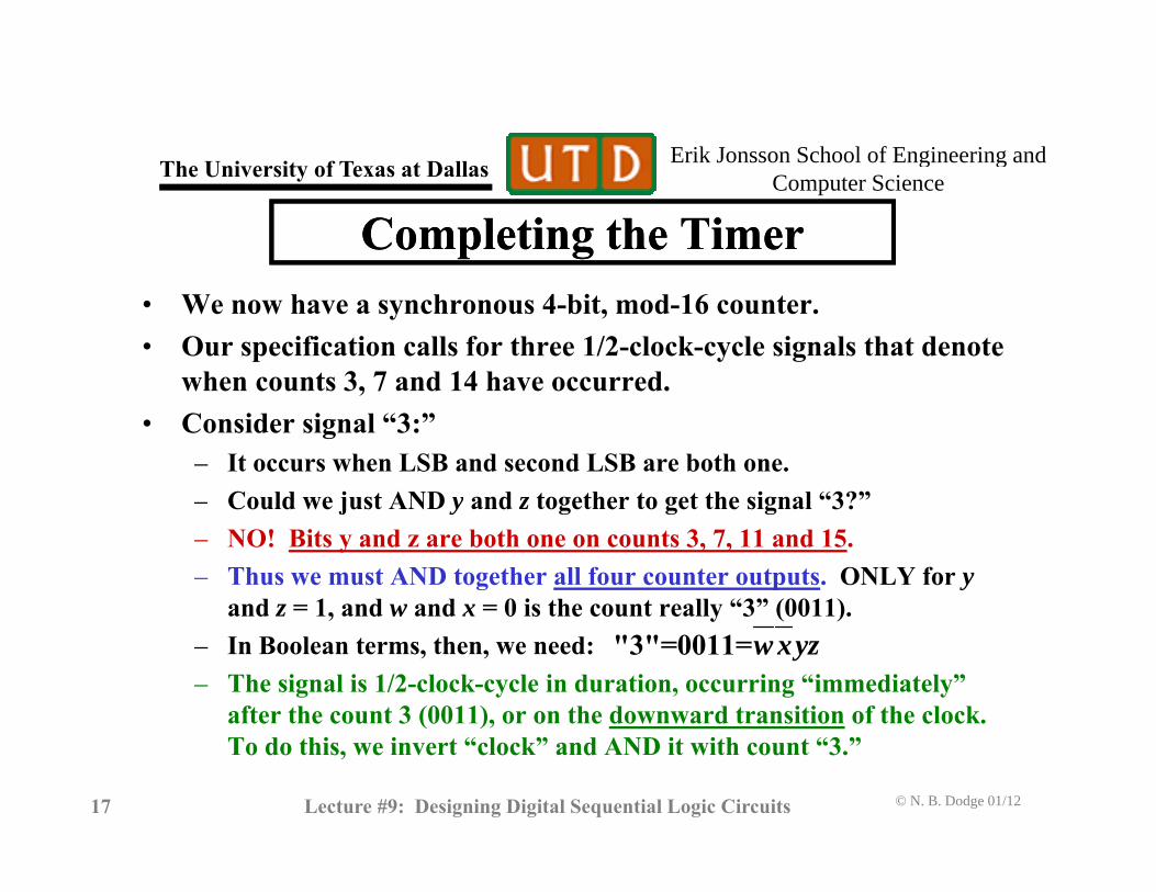
Completing the TimerCompleting the Timer• We now have a synchronous 4-bit, mod-16 counter. • Our specification calls for three 1/2-clock-cycle signals that denote
when counts 3, 7 and 14 have occurred.when counts 3, 7 and 14 have occurred. • Consider signal “3:”
– It occurs when LSB and second LSB are both one. – Could we just AND y and z together to get the signal “3?”– Could we just AND y and z together to get the signal 3?– NO! Bits y and z are both one on counts 3, 7, 11 and 15. – Thus we must AND together all four counter outputs. ONLY for y
and z = 1, and w and x = 0 is the count really “3” (0011).and z 1, and w and x 0 is the count really 3 (0011). – In Boolean terms, then, we need: – The signal is 1/2-clock-cycle in duration, occurring “immediately”
after the count 3 (0011), or on the downward transition of the clock.
"3"=0011=w xyz
© N. B. Dodge 01/12Lecture #9: Designing Digital Sequential Logic Circuits17
( ),To do this, we invert “clock” and AND it with count “3.”
Erik Jonsson School of Engineering and Th U i it f T t D ll g gComputer ScienceThe University of Texas at Dallas
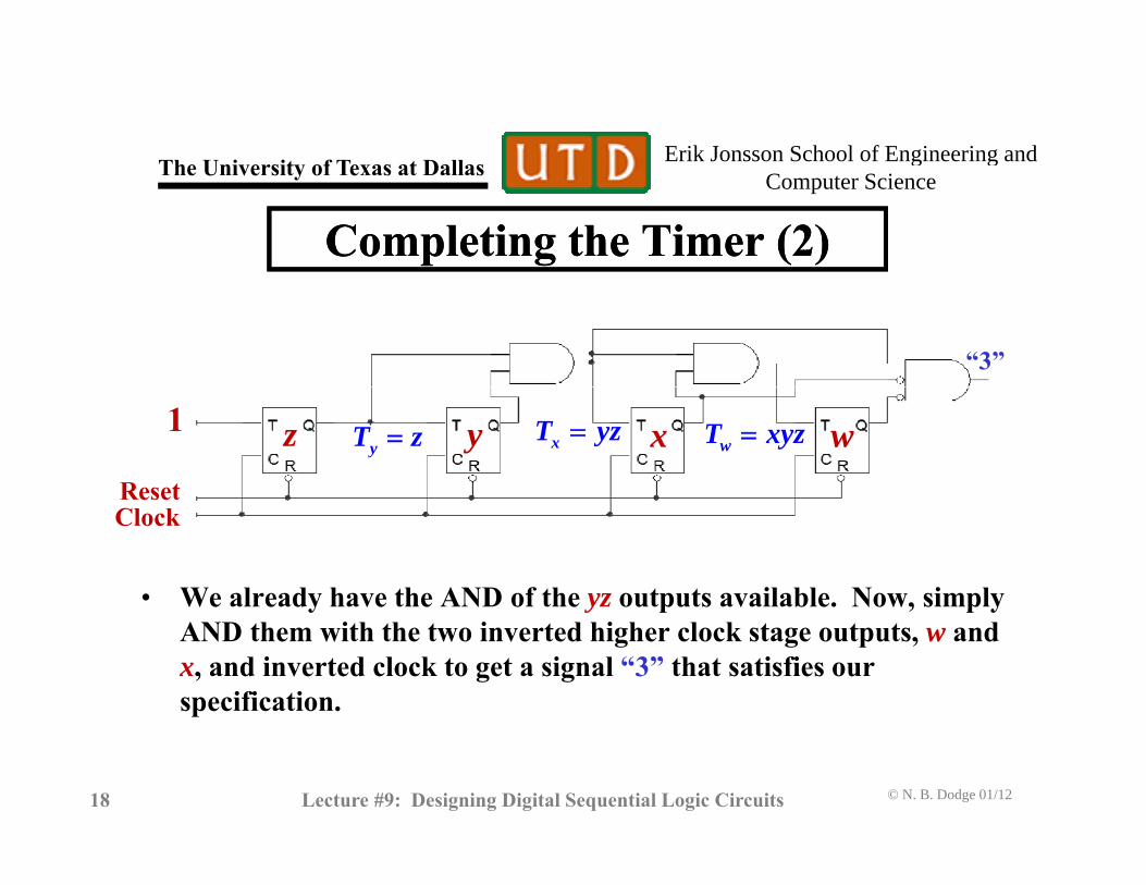
Completing the Timer (2)Completing the Timer (2)
“3”
y x w1 zReset
yT z xT yz wT xyz
• We already have the AND of the yz outputs available. Now, simply
ClockReset
y y p , p yAND them with the two inverted higher clock stage outputs, w and x, and inverted clock to get a signal “3” that satisfies our specification.
© N. B. Dodge 01/12Lecture #9: Designing Digital Sequential Logic Circuits18
Erik Jonsson School of Engineering and Th U i it f T t D ll g gComputer ScienceThe University of Texas at Dallas
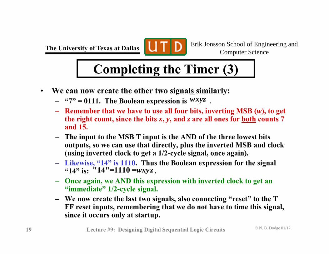
Completing the Timer (3)Completing the Timer (3)• We can now create the other two signals similarly:
– “7” = 0111. The Boolean expression is .Remember that we have to use all four bits inverting MSB (w) to get
wxyz– Remember that we have to use all four bits, inverting MSB (w), to get
the right count, since the bits x, y, and z are all ones for both counts 7 and 15.
– The input to the MSB T input is the AND of the three lowest bits t t th t di tl l th i t d MSB d l koutputs, so we can use that directly, plus the inverted MSB and clock
(using inverted clock to get a 1/2-cycle signal, once again). – Likewise, “14” is 1110. Thus the Boolean expression for the signal
“14” is: . "14"=1110 =wxyz– Once again, we AND this expression with inverted clock to get an
“immediate” 1/2-cycle signal. – We now create the last two signals, also connecting “reset” to the T
FF reset inputs remembering that we do not have to time this signal
© N. B. Dodge 01/12Lecture #9: Designing Digital Sequential Logic Circuits19
FF reset inputs, remembering that we do not have to time this signal, since it occurs only at startup.
Erik Jonsson School of Engineering and Th U i it f T t D ll g gComputer ScienceThe University of Texas at Dallas
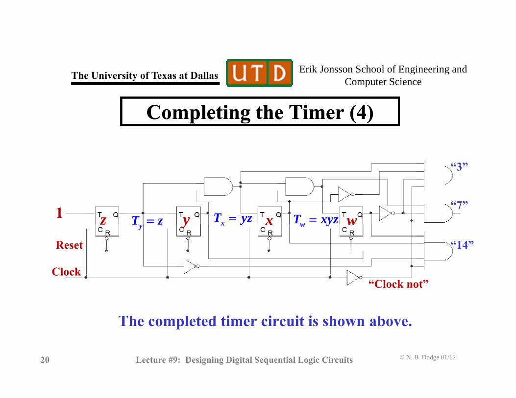
Completing the Timer (4)Completing the Timer (4)
“3”
y x w1 z T z xT yz wT xyz“7”
y x wz
Clock
Reset
yT z x y w yz
“14”
The completed timer circuit is shown above.
Clock“Clock not”
© N. B. Dodge 01/12Lecture #9: Designing Digital Sequential Logic Circuits20
The completed timer circuit is shown above.
Erik Jonsson School of Engineering and Th U i it f T t D ll g gComputer ScienceThe University of Texas at Dallas
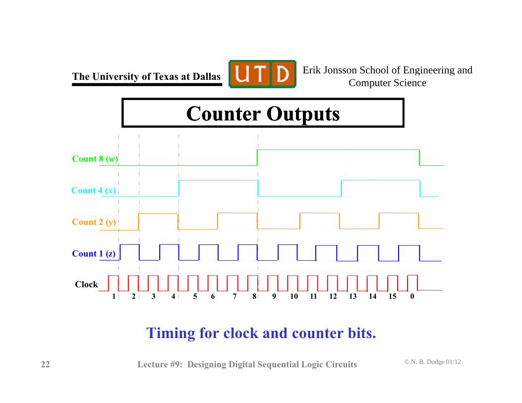
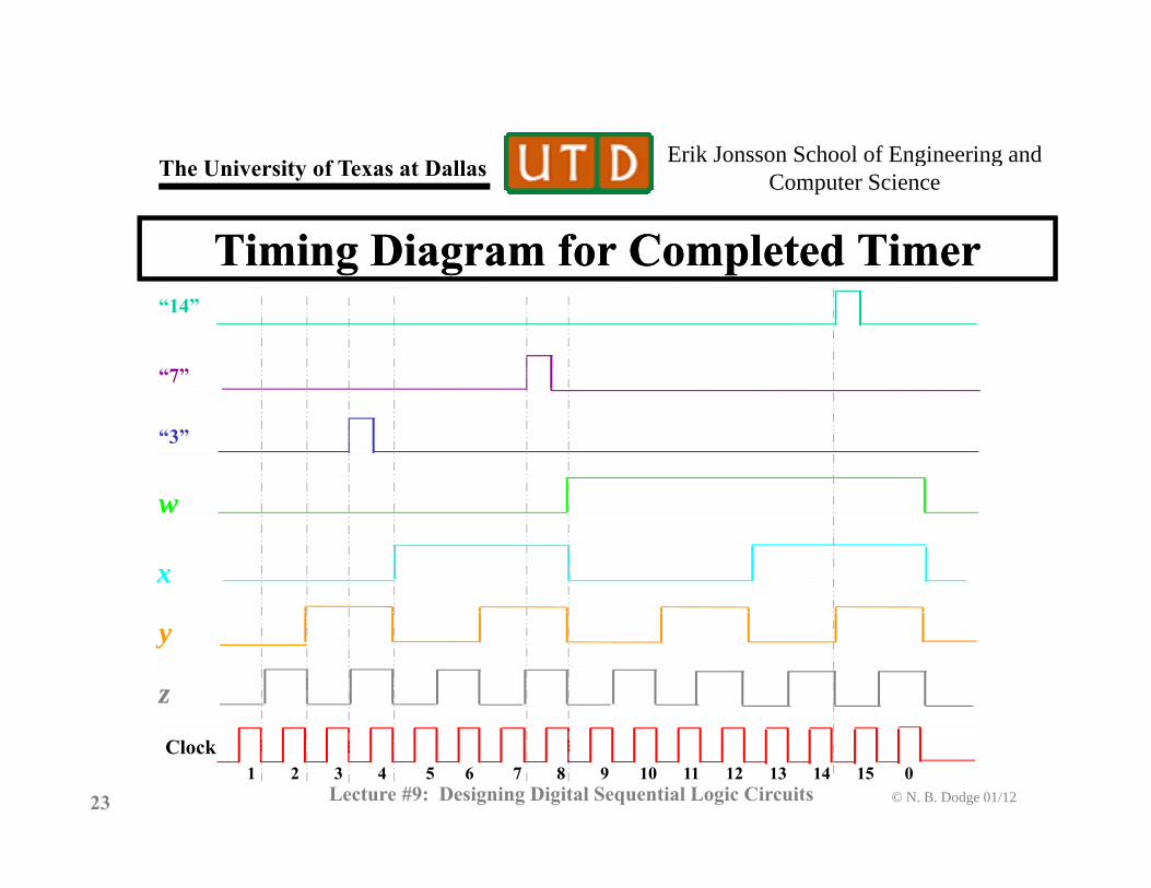
Completing the Timer (5)Completing the Timer (5)• We now want to show the timing for our counter/timer circuit, to
ensure that it meets the specification. All ti i i d ith t t th l k W fi t b ild th• All timing is done with respect to the clock. We first build the basic timing diagram for counter outputs (we do not time “Reset,” since the reset pulse occurs only at the start-up). Th ti i f l k d th f t t t i h th• The timing of clock and the four counter outputs is shown on the following slide.
• On the subsequent slide, we add the timing for the three signals th t h t d “3 ” “7 ” d “14 ”that we have created, “3,” “7,” and “14:” – “3” is true for 1/2 cycle on counter output 0011, “7” is true on count
0111, and “14” is true on count 1110 (all signals are ½ clock cycle).
© N. B. Dodge 01/12Lecture #9: Designing Digital Sequential Logic Circuits21
Erik Jonsson School of Engineering and Th U i it f T t D ll g gComputer ScienceThe University of Texas at Dallas
Counter OutputsCounter Outputs
Count 8 (w)
Count 4 (x)
Count 2 (y)
Count 1 (z)
Ti i f l k d t bit
Clock1 2 3 4 5 6 7 8 9 10 11 12 13 14 15 0
© N. B. Dodge 01/12Lecture #9: Designing Digital Sequential Logic Circuits22
Timing for clock and counter bits.
Erik Jonsson School of Engineering and Th U i it f T t D ll g gComputer ScienceThe University of Texas at Dallas
Timing Diagram for Completed TimerTiming Diagram for Completed Timer“14”
“7”
w
“3”
x
w
y
z
© N. B. Dodge 01/12Lecture #9: Designing Digital Sequential Logic Circuits23
Clock1 2 3 4 5 6 7 8 9 10 11 12 13 14 15 0
Erik Jonsson School of Engineering and Th U i it f T t D ll g gComputer ScienceThe University of Texas at Dallas
Design #2 – A “Sequential” MultiplexerDesign #2 – A “Sequential” Multiplexer• Our second “design project” is a sequential multiplexer. • A multiplexer (or MUX) is a combinational logic circuit that can
switch (or “gate”) one of several inputs onto a common output. The input which is gated to the output line depends on an address bus.
• Our sequential MUX is specified as follows:– Switches four inputs, a-d, onto a common output, each on a specific count. – A four-bit address sets the count for each input to be gated to the output.– The address consists of the outputs of a 4-bit synchronous counter.– The counter address goes from 0000 to 1111 (0x 0 to f, or modulo-16).– Input a is switched on count 3, input b on count 7, input c on count 11,
and input d is switched to the output on count 15.
© N. B. Dodge 01/12Lecture #9: Designing Digital Sequential Logic Circuits24
– Each input stays connected to the output for the duration of that count.
Erik Jonsson School of Engineering and Th U i it f T t D ll g gComputer ScienceThe University of Texas at Dallas
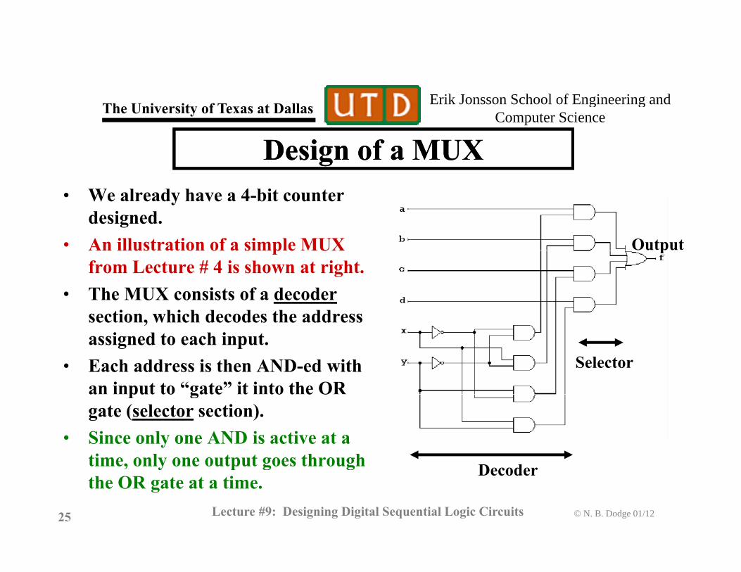
Design of a MUXDesign of a MUX• We already have a 4-bit counter
designed. • An illustration of a simple MUX OutputAn illustration of a simple MUX
from Lecture # 4 is shown at right. • The MUX consists of a decoder
section, which decodes the address
Ou pu
section, which decodes the address assigned to each input.
• Each address is then AND-ed with an input to “gate” it into the OR
Selectora put to gate t to t e Ogate (selector section).
• Since only one AND is active at a time, only one output goes through D d
© N. B. Dodge 01/12Lecture #9: Designing Digital Sequential Logic Circuits25
, y p g gthe OR gate at a time.
Decoder
Erik Jonsson School of Engineering and Th U i it f T t D ll g gComputer ScienceThe University of Texas at Dallas
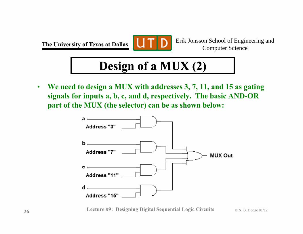
Design of a MUX (2)Design of a MUX (2)• We need to design a MUX with addresses 3, 7, 11, and 15 as gating
signals for inputs a, b, c, and d, respectively. The basic AND-OR part of the MUX (the selector) can be as shown below:
© N. B. Dodge 01/12Lecture #9: Designing Digital Sequential Logic Circuits26
Erik Jonsson School of Engineering and Th U i it f T t D ll g gComputer ScienceThe University of Texas at Dallas
Design of a MUX (3)Design of a MUX (3)
• We now need to provide our basic combinational logic MUX with the four switching addresses 3, 7, 11, and 15. This can be the decoded outputs of our already-designed 4-bit counter.
• However, we need to decode two different outputs from the ones that we put together for our first timer.
• Also, our decoded signals now need to last a full clock cycle, NOT 1/2 cycle.
• Since each of the 16 counts of the counter lasts exactly one clock S ce e c o e 6 cou s o e cou e s s e c y o e c ocperiod, we no longer need the clock input to be AND-ed with the count.
• We therefore need only to decode the clock counts 3, 7, 11, and 15.
© N. B. Dodge 01/12Lecture #9: Designing Digital Sequential Logic Circuits27
y , , ,
Erik Jonsson School of Engineering and Th U i it f T t D ll g gComputer ScienceThe University of Texas at Dallas
Exercise 3 – MUX Address DecodesExercise 3 – MUX Address Decodes• From our first exercise, we know that all four counter
bits must be used to decode each output count. • Assuming w = MSB, z = LSB, compose the Boolean
expressions for the counter states 3, 7, 11, and 15 on which the MUX outputs are madewhich the MUX outputs are made.
© N. B. Dodge 01/12Lecture #9: Designing Digital Sequential Logic Circuits28
Erik Jonsson School of Engineering and Th U i it f T t D ll g gComputer ScienceThe University of Texas at Dallas
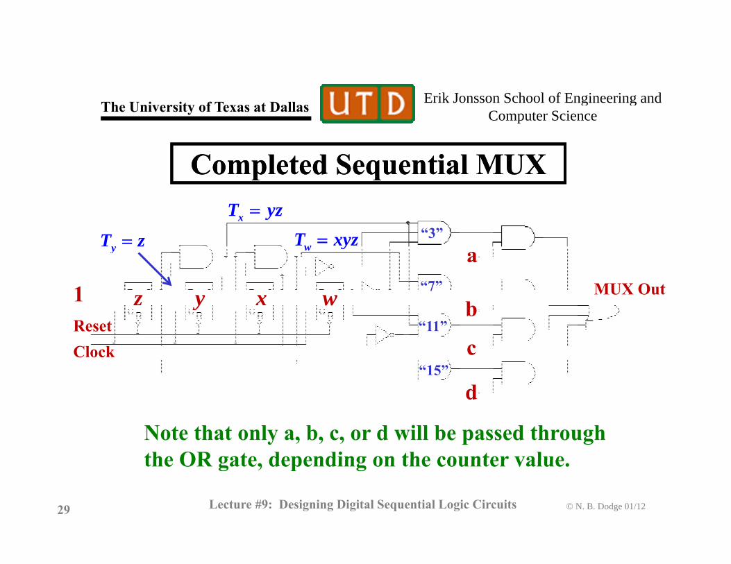
Completed Sequential MUXCompleted Sequential MUXp qp qxT yz
wT xyz “3”yT z
y x w1 z
w yz
MUX Out“7”
y za
b
ClockReset “11”
“15”c
d
Note that only a, b, c, or d will be passed through the OR gate depending on the counter value
d
© N. B. Dodge 01/12Lecture #9: Designing Digital Sequential Logic Circuits29
the OR gate, depending on the counter value.
Erik Jonsson School of Engineering and Th U i it f T t D ll g gComputer ScienceThe University of Texas at Dallas
MUX TimingMUX Timing
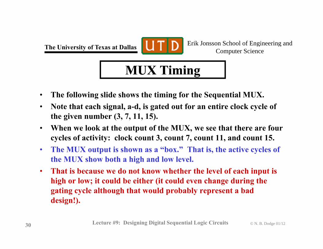
• The following slide shows the timing for the Sequential MUX.• Note that each signal, a-d, is gated out for an entire clock cycle ofNote that each signal, a d, is gated out for an entire clock cycle of
the given number (3, 7, 11, 15). • When we look at the output of the MUX, we see that there are four
cycles of activity: clock count 3, count 7, count 11, and count 15.cycles of activity: clock count 3, count 7, count 11, and count 15.• The MUX output is shown as a “box.” That is, the active cycles of
the MUX show both a high and low level.• That is because we do not know whether the level of each input is• That is because we do not know whether the level of each input is
high or low; it could be either (it could even change during the gating cycle although that would probably represent a bad design!).
© N. B. Dodge 01/12Lecture #9: Designing Digital Sequential Logic Circuits30
g )
Erik Jonsson School of Engineering and Th U i it f T t D ll g gComputer ScienceThe University of Texas at Dallas
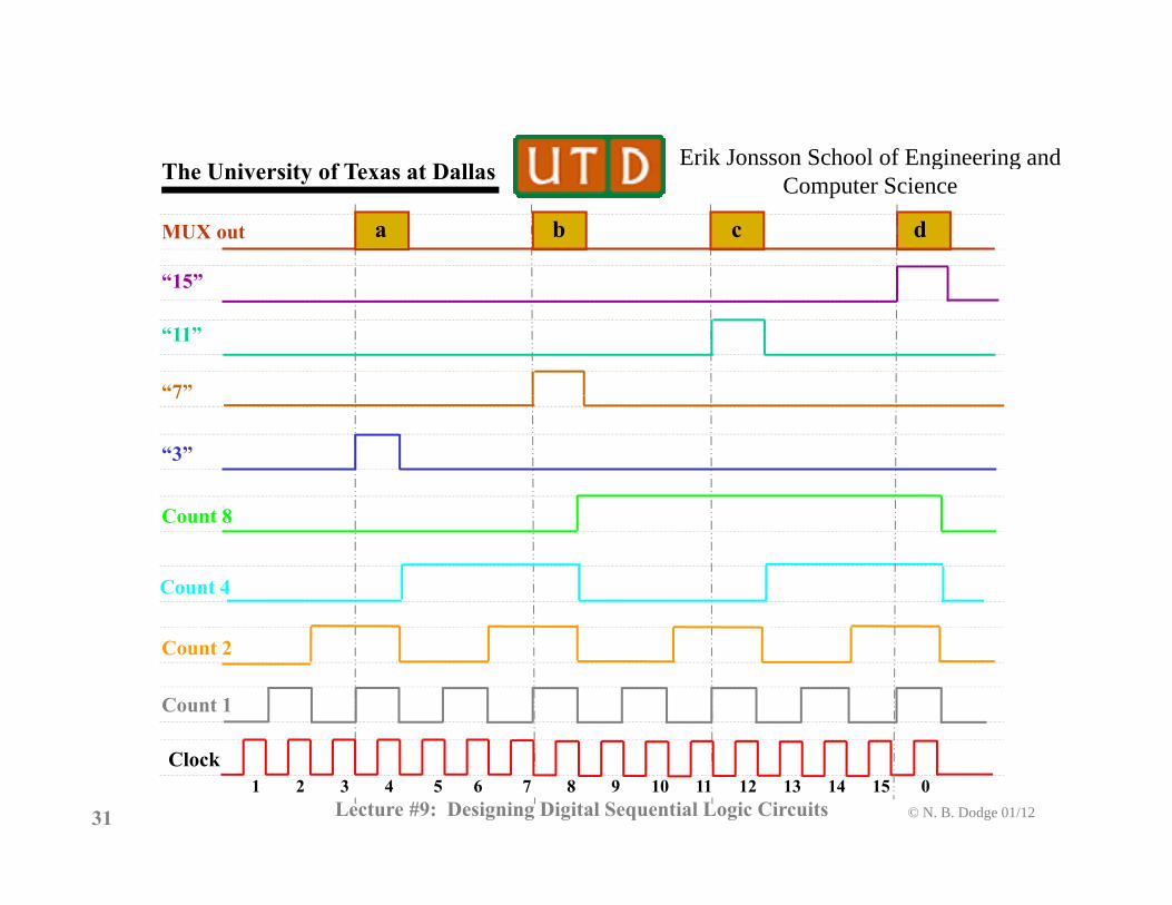
“15”
MUX out a b c d
“11”
“7”
15
C t 8
7
“3”
Count 4
Count 8
Count 2
Count 1
© N. B. Dodge 01/12Lecture #9: Designing Digital Sequential Logic Circuits31
Clock1 2 3 4 5 6 7 8 9 10 11 12 13 14 15 0
Erik Jonsson School of Engineering and Th U i it f T t D ll g gComputer ScienceThe University of Texas at Dallas
Final Design -- Decimal CounterFinal Design -- Decimal Counter• Our specification is for a decimal counter, that is, one that counts
“modulo ten.” • This is a realistic design, since in many electronic devices orThis is a realistic design, since in many electronic devices or
appliances, it is often necessary to count in tens. • We will design only a single 0-9 counter, recognizing that we can
count to 99 or 999 by simply including additional counter digits.count to 99 or 999 by simply including additional counter digits.• We already have a 4-bit counter (counting up to 9 requires 4 bits),
so all we have to do is modify it to count decimal. • The counter must:• The counter must:
– Count from zero to nine and reset on the tenth clock pulse. – Count synchronously (as usual), that is, in parallel, not ripple.
Have the four counter bits available as outputs so that they might be
© N. B. Dodge 01/12Lecture #9: Designing Digital Sequential Logic Circuits32
– Have the four counter bits available as outputs, so that they might be decoded to indicate various counts, from 0 to 9.
Erik Jonsson School of Engineering and Th U i it f T t D ll g gComputer ScienceThe University of Texas at Dallas
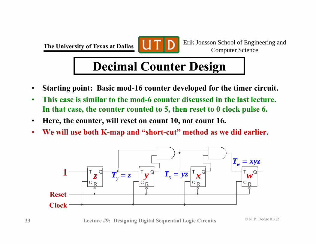
Decimal Counter DesignDecimal Counter Design• Starting point: Basic mod-16 counter developed for the timer circuit. • This case is similar to the mod-6 counter discussed in the last lecture.
I th t th t t d t 5 th t t 0 l k l 6In that case, the counter counted to 5, then reset to 0 clock pulse 6.• Here, the counter, will reset on count 10, not count 16.• We will use both K-map and “short-cut” method as we did earlier.
wT xyz
y x w1 z
Reset
yT z xT yz
© N. B. Dodge 01/12Lecture #9: Designing Digital Sequential Logic Circuits33
Clock
Erik Jonsson School of Engineering and Th U i it f T t D ll g gComputer ScienceThe University of Texas at Dallas
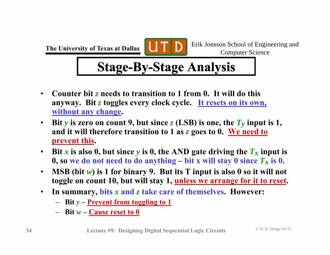
Stage-By-Stage AnalysisStage-By-Stage Analysis
• Counter bit z needs to transition to 1 from 0. It will do this anyway. Bit z toggles every clock cycle. It resets on its own, without any changewithout any change.
• Bit y is zero on count 9, but since z (LSB) is one, the Ty input is 1, and it will therefore transition to 1 as z goes to 0. We need to prevent this. p
• Bit x is also 0, but since y is 0, the AND gate driving the Tx input is 0, so we do not need to do anything – bit x will stay 0 since Tx is 0.
• MSB (bit w) is 1 for binary 9. But its T input is also 0 so it will not ( ) y ptoggle on count 10, but will stay 1, unless we arrange for it to reset.
• In summary, bits x and z take care of themselves. However:– Bit y – Prevent from toggling to 1
© N. B. Dodge 01/12Lecture #9: Designing Digital Sequential Logic Circuits34
– Bit w – Cause reset to 0
Erik Jonsson School of Engineering and Th U i it f T t D ll g gComputer ScienceThe University of Texas at Dallas
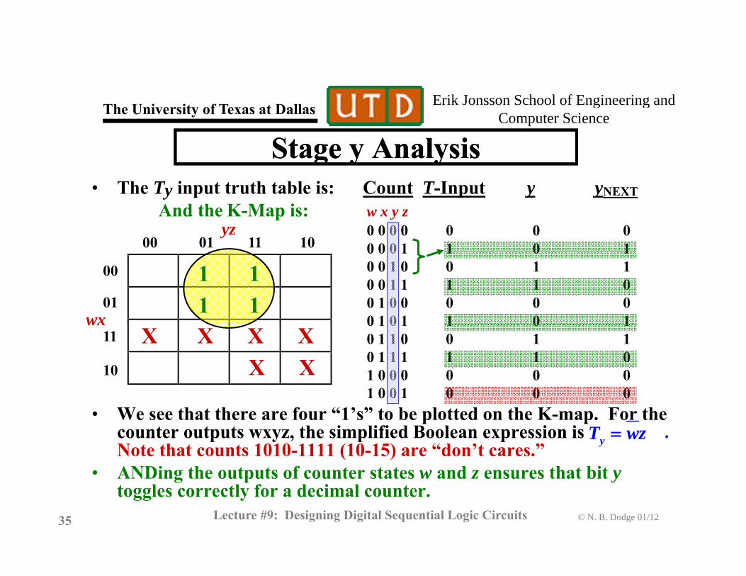
Stage y AnalysisStage y Analysis• The Ty input truth table is: Count T-Input y yNEXT
And the K-Map is: w x y z0 0 0 0 0 0 00 0 0 1 1 0 1
yz00 01 11 10 0 0 0 1 1 0 1
0 0 1 0 0 1 10 0 1 1 1 1 00 1 0 0 0 0 00 1 0 1 1 0 1
1
1
1
1
wx
00
01
1 11 1
0 1 0 1 1 0 10 1 1 0 0 1 10 1 1 1 1 1 01 0 0 0 0 0 01 0 0 1 0 0 0
wx11
10
X X X XX X
1 0 0 1 0 0 0• We see that there are four “1’s” to be plotted on the K-map. For the
counter outputs wxyz, the simplified Boolean expression is . Note that counts 1010-1111 (10-15) are “don’t cares.”ANDi th t t f t t t d th t bit
yT wz
© N. B. Dodge 01/12Lecture #9: Designing Digital Sequential Logic Circuits35
• ANDing the outputs of counter states w and z ensures that bit ytoggles correctly for a decimal counter.
Erik Jonsson School of Engineering and Th U i it f T t D ll g gComputer ScienceThe University of Texas at Dallas
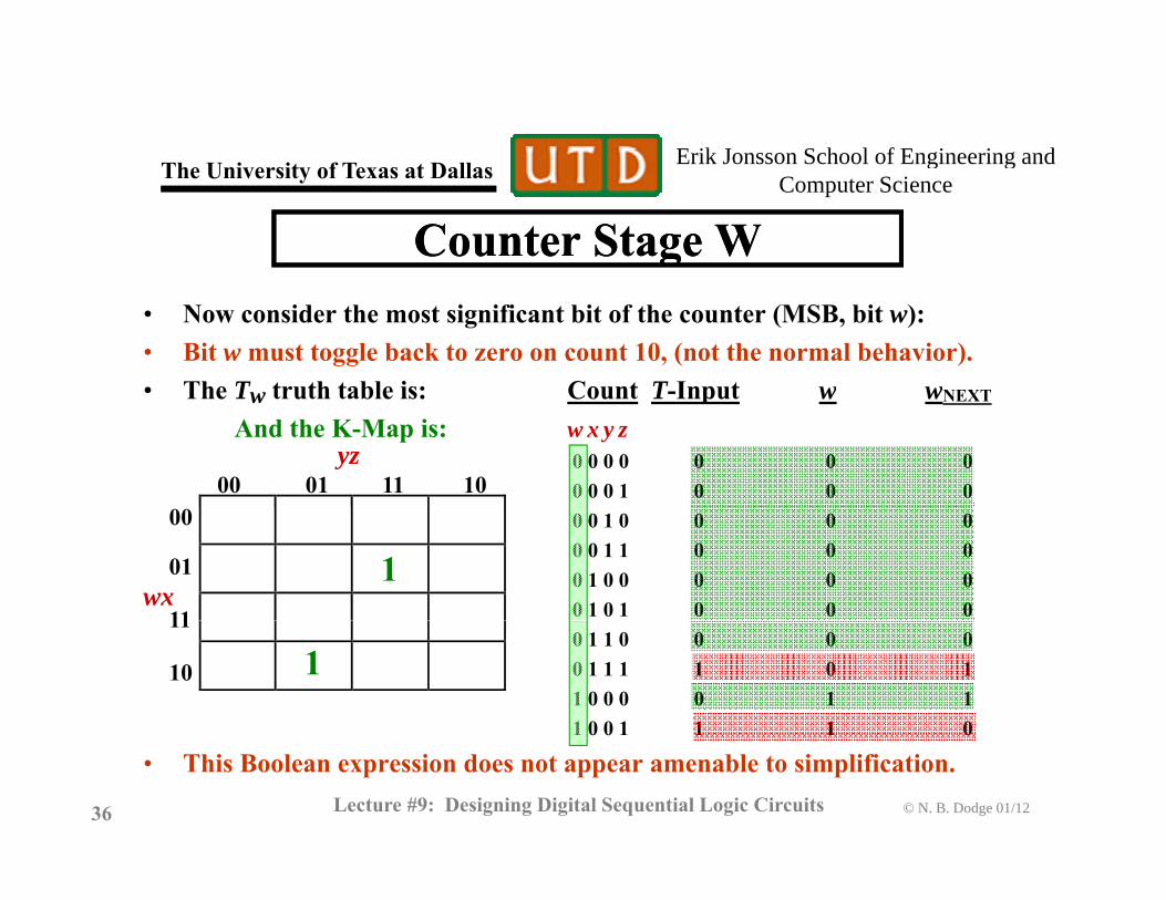
Counter Stage WCounter Stage W• Now consider the most significant bit of the counter (MSB, bit w):• Bit w must toggle back to zero on count 10, (not the normal behavior).• The Tw truth table is: Count T-Input w wNEXTThe Tw truth table is: Count T-Input w wNEXT
And the K-Map is: w x y z0 0 0 0 0 0 00 0 0 1 0 0 0
yz00 01 11 10
0 0 1 0 0 0 00 0 1 1 0 0 00 1 0 0 0 0 00 1 0 1 0 0 0
1wx
00
01
11
1
0 1 1 0 0 0 00 1 1 1 1 0 11 0 0 0 0 1 11 0 0 1 1 1 0
1
11
10 1
© N. B. Dodge 01/12Lecture #9: Designing Digital Sequential Logic Circuits36
1 0 0 1 1 1 0
• This Boolean expression does not appear amenable to simplification.
Erik Jonsson School of Engineering and Th U i it f T t D ll g gComputer ScienceThe University of Texas at Dallas
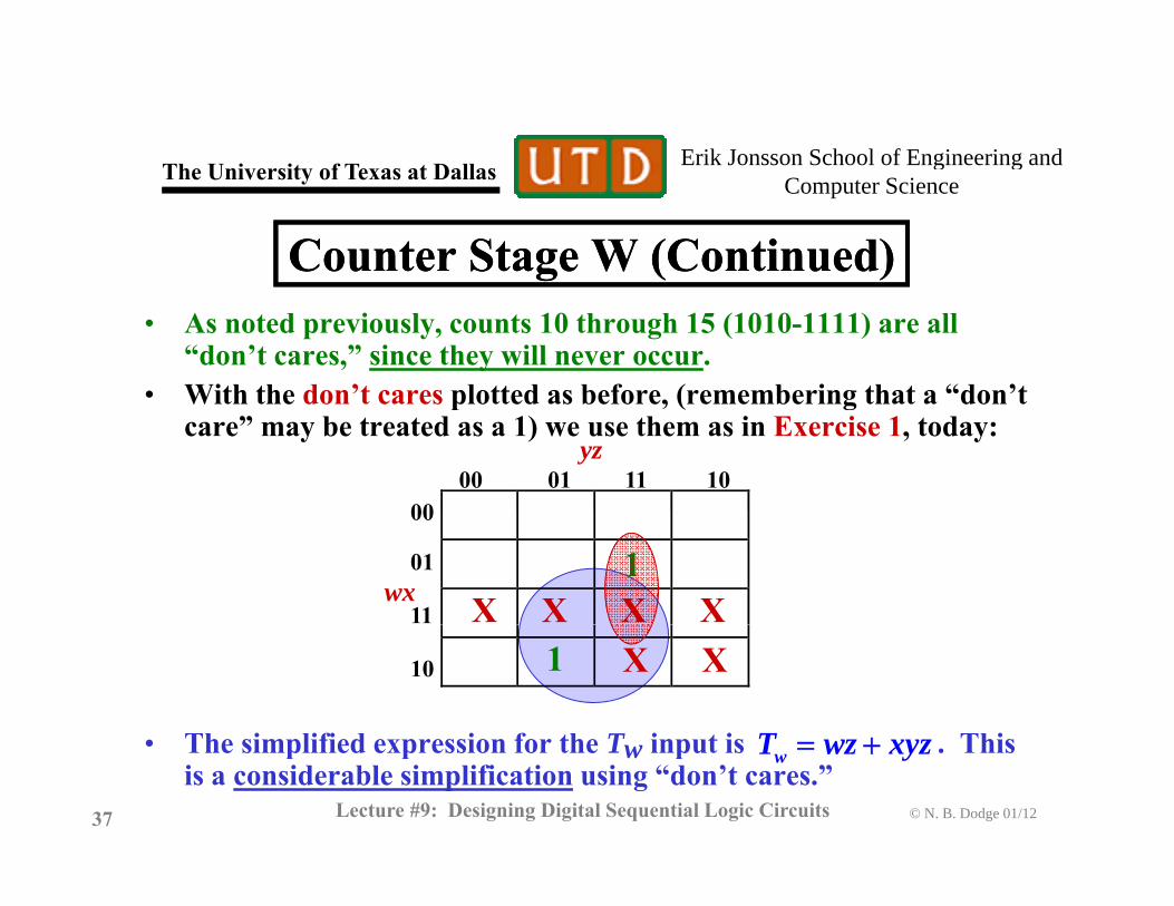
Counter Stage W (Continued)Counter Stage W (Continued)• As noted previously, counts 10 through 15 (1010-1111) are all
“don’t cares,” since they will never occur. • With the don’t cares plotted as before (remembering that a “don’t• With the don t cares plotted as before, (remembering that a don t
care” may be treated as a 1) we use them as in Exercise 1, today: yz
00 01 11 1000
1wx
00
01
11
1X X X X
The simplified e pression for the T inp t is This
110 1 X X
T
© N. B. Dodge 01/12Lecture #9: Designing Digital Sequential Logic Circuits37
• The simplified expression for the Tw input is . This is a considerable simplification using “don’t cares.”
wT wz xyz
Erik Jonsson School of Engineering and Th U i it f T t D ll g gComputer ScienceThe University of Texas at Dallas
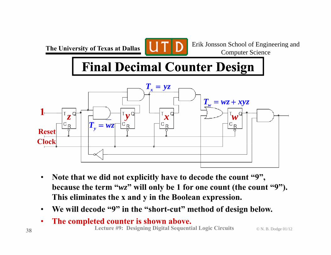
Final Decimal Counter DesignFinal Decimal Counter Design
1
xT yz
wT wz xyz
y x w1 z
ClockReset yT wz
N t th t did t li itl h t d d th t “9”
Clock
• Note that we did not explicitly have to decode the count “9”, because the term “wz” will only be 1 for one count (the count “9”). This eliminates the x and y in the Boolean expression. We will decode “9” in the “short cut” method of design below
© N. B. Dodge 01/12Lecture #9: Designing Digital Sequential Logic Circuits38
• We will decode “9” in the “short-cut” method of design below. • The completed counter is shown above.
Erik Jonsson School of Engineering and Th U i it f T t D ll g gComputer ScienceThe University of Texas at Dallas
Using the “Short-Cut” Approach (m≠2n)Using the “Short-Cut” Approach (m≠2n)• We previously learned a second “short cut” method to
design a mod-m counter, m not a power of 2. Th “ h t t” l• The “short cut” rules are: – To count any number m, m not a power of 2, determine the
smallest mod 2n counter such that 2n >m. B ild th ll l 2n t d ib d i l– Build the parallel 2n counter as described previously.
– Determine stages that will → 1 on count m, and those that stay at 1 on count m (some stages may not need any “help”). Using the outputs of the 2n counter decode (m 1)– Using the outputs of the 2n counter, decode (m-1).
– For each stage of the 2n counter that remains at 1 on count m, (has a 0 T-input on count m-1), OR the current T-input with decoded (m-1). For each stage that will → 1 on count m (T
© N. B. Dodge 01/12Lecture #9: Designing Digital Sequential Logic Circuits39
decoded (m 1). For each stage that will 1 on count m (T input of 1), AND inverted (m-1) with that current T-input.
Erik Jonsson School of Engineering and Th U i it f T t D ll g gComputer ScienceThe University of Texas at Dallas
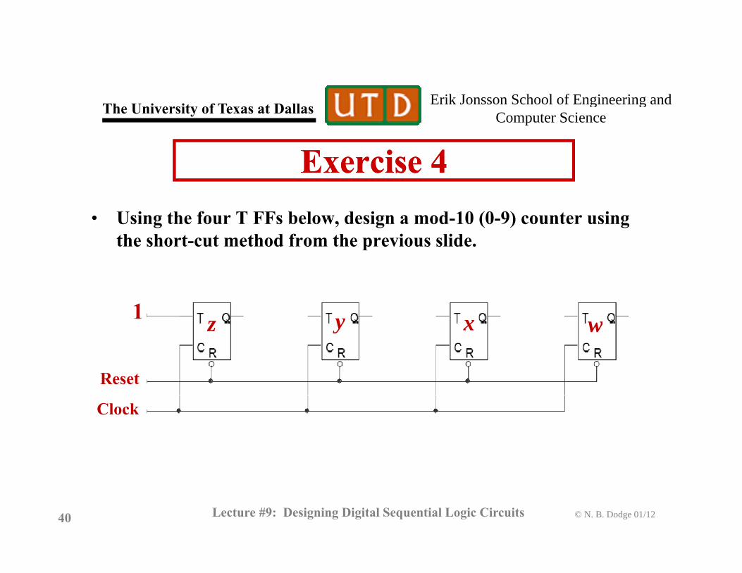
Exercise 4Exercise 4• Using the four T FFs below, design a mod-10 (0-9) counter using
the short-cut method from the previous slide.
y x w1 z y x wz
Reset
Clock
© N. B. Dodge 01/12Lecture #9: Designing Digital Sequential Logic Circuits40
Erik Jonsson School of Engineering and Th U i it f T t D ll g gComputer ScienceThe University of Texas at Dallas
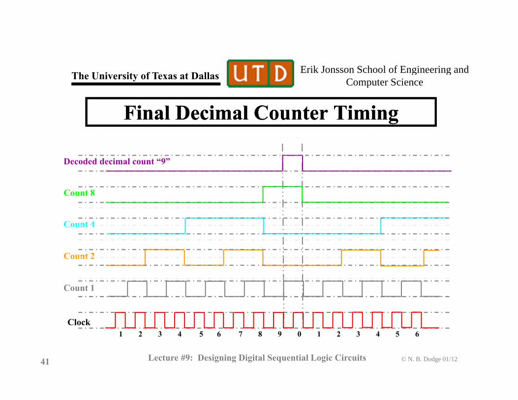
Final Decimal Counter TimingFinal Decimal Counter Timing
Decoded decimal count “9”
Count 4
Count 8
Count 4
Count 2
Clock
Count 1
© N. B. Dodge 01/12Lecture #9: Designing Digital Sequential Logic Circuits41
1 2 3 4 5 6 7 8 9 0 1 2 3 4 5 6
Erik Jonsson School of Engineering and Th U i it f T t D ll g gComputer ScienceThe University of Texas at Dallas
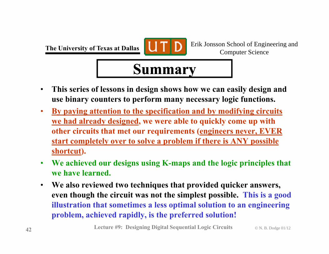
SummarySummary• This series of lessons in design shows how we can easily design and
use binary counters to perform many necessary logic functions. • By paying attention to the specification and by modifying circuits• By paying attention to the specification and by modifying circuits
we had already designed, we were able to quickly come up with other circuits that met our requirements (engineers never, EVER start completely over to solve a problem if there is ANY possiblestart completely over to solve a problem if there is ANY possible shortcut).
• We achieved our designs using K-maps and the logic principles that we have learned.we have learned.
• We also reviewed two techniques that provided quicker answers, even though the circuit was not the simplest possible. This is a good illustration that sometimes a less optimal solution to an engineering
© N. B. Dodge 01/12Lecture #9: Designing Digital Sequential Logic Circuits42
illustration that sometimes a less optimal solution to an engineering problem, achieved rapidly, is the preferred solution!
Erik Jonsson School of Engineering and Th U i it f T t D ll g gComputer ScienceThe University of Texas at Dallas
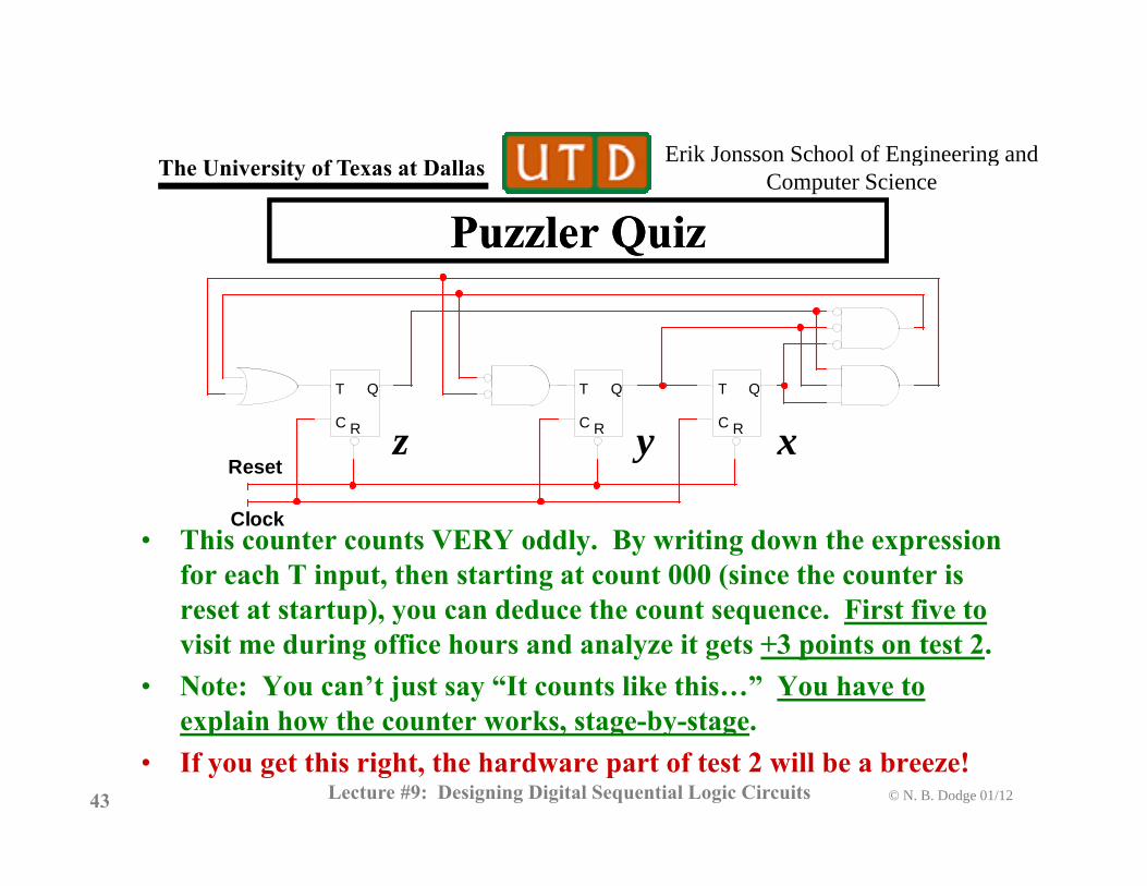
Puzzler QuizPuzzler Quiz
T Q T Q T Q
Z y X
Reset
T
C R
Q T
C R
Q T
C R
Q
z y x
• This counter counts VERY oddly. By writing down the expression for each T input, then starting at count 000 (since the counter is reset at startup) you can deduce the count sequence First five to
Clock
reset at startup), you can deduce the count sequence. First five to visit me during office hours and analyze it gets +3 points on test 2.
• Note: You can’t just say “It counts like this…” You have to explain how the counter works stage-by-stage
© N. B. Dodge 01/12Lecture #9: Designing Digital Sequential Logic Circuits43
explain how the counter works, stage-by-stage. • If you get this right, the hardware part of test 2 will be a breeze!