
Oxymoron: a posh mutt Alliteration: a posh pug parades in Piccadilly Square

ERI Design: IDEA and POSHALIGN: Analog Layout, Intelligently Generated from Netlists
IDEA and POSH Phase I Integration Meeting
Detroit, Michigan
17 July 2019– 19 July 2019
University of Minnesota (Prime)Texas A&M
Intel
Fundamental Research

Team Members at the Integration Meeting
Fundamental Research 2
Sachin Sapatnekar
Ramesh Harjani
Jiang HuSteve Burns
Wenbin Xu
TonmoyDhar
KishorKunal
Meghna Madhusudan
Arvind Sharma
ParijatMukherjee
Jitesh Poojary
Yaguang Li

Goal: No-human-in-the-loop layout generation from netlist to GDSII.
Overview
Proprietary
Proprietary
OPEN-SOURCE
Fundamental Research 3
Technical Approach

Goal: No-human-in-the-loop layout generation from netlist to GDSII.
Overview
Proprietary
Proprietary
OPEN-SOURCE
Fundamental Research 4
Technical Approach

The ALIGN Github Repo: Alpha Release
Fundamental Research 5
https://github.com/ALIGN‐analoglayout/ALIGN‐public

The ALIGN Github Repo: Alpha Release
Fundamental Research 6
https://github.com/ALIGN‐analoglayout/ALIGN‐public

Classification of Analog Circuits: Layout Compiler
Fundamental Research
Act
ive
Mat
chin
g
Pass
ive
Mat
chin
g
Noi
se
Sens
itivi
ty
Indu
ctor
s
Para
sitic
s
Low Frequency Analog
Power Delivery
Wireline
Wireless
Not critical
Critical
7
Eg. OTA, Switched Capacitor Filter
Eg. Mixer, Oscillator
Eg. Equalizer
Eg. Buck Converter
ALIGN target circuits: Low-frequency analog, wireline, wireless, power delivery

DEMO: OTA
Differential pair
Current mirror
Fundamental Research
Common centroid
DRC correct by construction
SymmetryA ABB
Axis of symmetry
Matching
Symmetric routing
Current mirror
Diff
eren
tial
pair
Telescopic OTA
8
Primitive layout generation
Netlist Annotation
Block Assembly

Switched Capacitor Filter
DEMO: Switched Capacitor Filter
Switch
Differential Pair (OTA Primitives)
Capacitor Array (common centroid)
Unit C
Fundamental Research
Telescopic OTA
Differential pair
Current mirror
9
C2
C2
CL
CLC1
C1OTA
CA
C3
C3
CA

Performance Analysis: Switched Capacitor Filter
Specification Unit Schematic Post – Layout Shift
Inband gain dB 5.53 5.48 -1 %
Fundamental Research
Switched Capacitor Filter
Telescopic OTA
Differential pair
Current mirror
10
C2
C2
CL
CLC1
C1OTA
CA
C3
C3
CA
[ASAP7nm]

Performance Analysis: OTA
Post - Layout(C only extract) Shift
39.29 0 %10.473 -2 %489.85 -1 %
0 -
Differential pair
Current mirror
Fundamental Research
Specification Unit Schematic Post – Layout(RC extract) Shift
AC Gain dB 39.295 37.25 -5 %3 dB frequency MHz 10.648 10.473 -2 %Unity Gain Frequency MHz 493.62 382.95 -22 %Input Offset mV 0 0.145 -
Telescopic OTA
11
[ASAP7nm]
Points to a 28% reduction in gm

Overall Design Flow
Electrical Constraint Generation
Block Assembly
(Placement and Routing)
Output: GDSII
ML models
Basic Cell Templates
Netlist auto-annotation
Input: Unannotated
Netlist
Primitive Cell
Generation
PDK
A
bstraction
User Defined Cell Templates
Input
Fundamental Research 12
PDK.json
PDK.json
Netlist.v Netlist.v
Block.lef + Block.json
Constraints
Data Formats
.sp
.json

Stages of the flow
Fundamental Research 13

Fundamental Research 14
Auto-annotation and the Concept of Hierarchy
Block Primitives
Switched Capacitor FilterTelescopic OTA
Differential pair
Current mirror
Sub block

Fundamental Research 15
Higher-level blocks have many variants – hard to enumerateThese are just a few types of OTAs:
Graph-based neural network: Key differentiator from prior approaches!Useful in identifying and annotating such structures with constraints (symmetry, common centroid,…)
Auto-annotation of Input Netlists

Recognizing Sub-blocks within a Switched-capacitor Filter
GCNNetlist
= OTA nodeɸ1
ɸ2
ɸ2 ɸ2
ɸ1 ɸ1
ɸ1
ɸ2
ɸ2 ɸ2
ɸ1 ɸ1
C2
C2
C3
C1
C1
C3
CA
C4
C4
CA
OTA
Fundamental Research 16
Graph
Fundamental Research 17
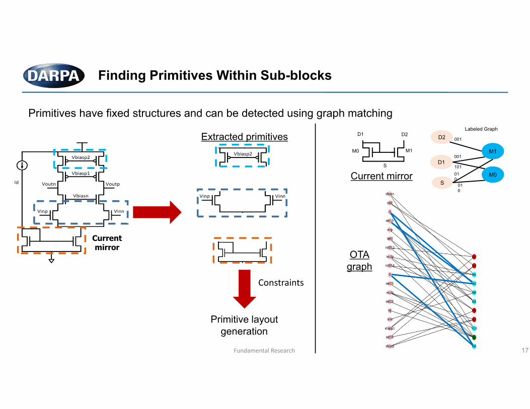
Primitives have fixed structures and can be detected using graph matching
Finding Primitives Within Sub-blocks
M0 M1
D1 D2
S
001
001
010
Labeled Graph
M0
D2
D1
S
M1
101
010
OTAgraph
Current mirror
Constraints
Current mirror
Primitive layoutgeneration
Extracted primitives

Fundamental Research 18
OTA BIAS
OTA 21 0
BIAS 1 35
GCN-based Recognition: Switched Capacitor Filter
Classification resultSwitched capacitor filter circuit
Actual Class
Pred
icte
d cl
ass

Fundamental Research 19
OTA BIAS
OTA 22 0
BIAS 0 35
GCN-based Recognition: Switched Capacitor Filter
Classification result after postprocessing
Switched capacitor filter circuit
Actual Class
Pred
icte
d cl
ass
Fundamental Research 20
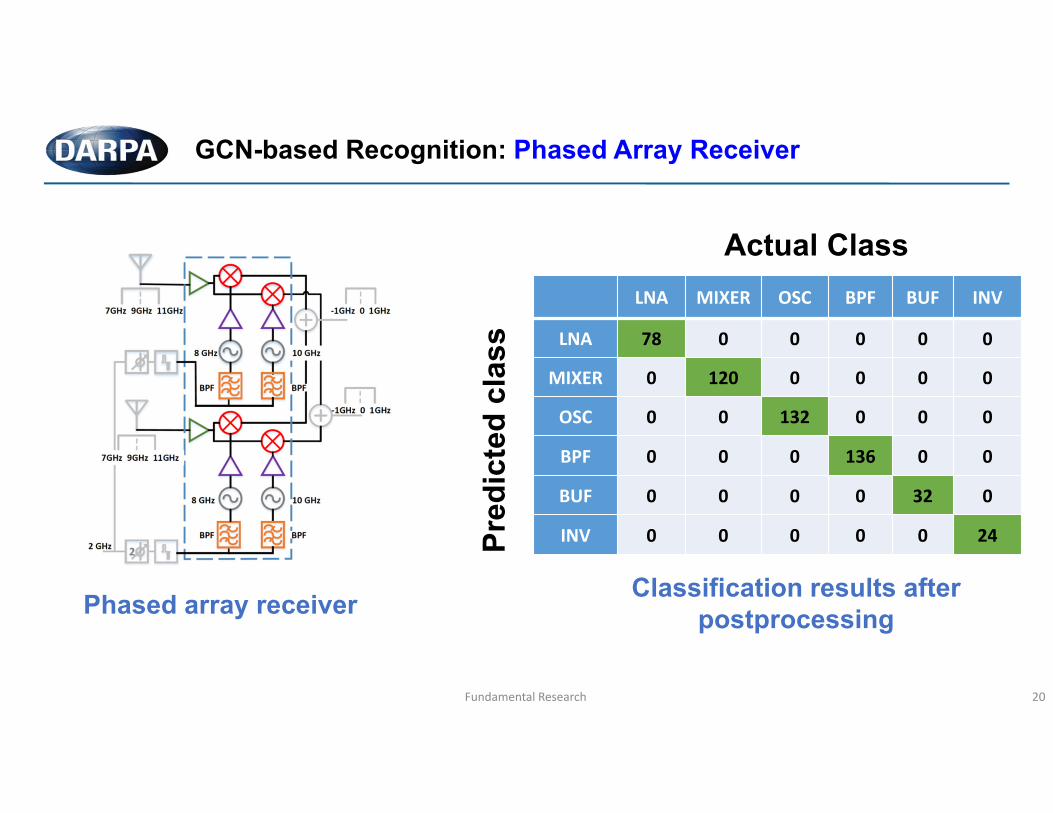
GCN-based Recognition: Phased Array Receiver
Phased array receiver Classification results after postprocessing
LNA MIXER OSC BPF BUF INV
LNA 78 0 0 0 0 0
MIXER 0 120 0 0 0 0
OSC 0 0 132 0 0 0
BPF 0 0 0 136 0 0
BUF 0 0 0 0 32 0
INV 0 0 0 0 0 24Pred
icte
d cl
ass
Actual Class

Philosophy: Simplify design by restricting layout onto gridsDistance-based design rules become enforced either:• By adherence of objects to the grid, or• By Boolean rules relating the presence/absence of objects on the grid Examples: Pitch, width and space, minimum end-to-end, via rules~8x reduction in the abstracted rules compared to PDK DRCs
PDK Abstraction: Concepts
Via-to-via rule: diagonal vias disallowed
Min End-to-End
Width
Pitch
Laye
r-spe
cific
grid
ding
[* Design rules for FinFET MockPDK available on ALIGN github]
Applied to• Commercial PDKs (FinFET: GF12/14,
Bulk: TSMC65), ASAP7, a FinFETMock PDK*
• Internally within Intel to 22, 14, 10, 7, 5, 3nm process technologies
Fundamental Research 21

Simpler regular grid generated from common code and process constants stored in JSON format
Adequate for GF12, ASAP7, TSMC65
PDK Abstraction: Creating Grids
"Layer": "M2",
"LayerNo": 8,
"Direction": "H",
"Color": ["c2", "c1"],
"Pitch": 84,
"Width": 32,
"MinL": 200,
"MaxL": null,
"EndToEnd": 48,
"Offset": 0
"Layer": "V2",
"LayerNo": 15,
"Stack": ["M2", "M3"],
"SpaceX": 76,
"SpaceY": 76,
"WidthX": 32,
"WidthY": 32,
"VencA_L": 20,
"VencA_H": 20,
"VencP_L": 0,
"VencP_H": 4,
"MinNo": 1
c = 0a = [w,m,m,n,n,n,m,m,w]for (u,v) in zip(a[:-1],a[1:]):
m0.addCenterLine( c, u)c += u//2 + s + v//2
m0.addCenterLine( c, a[-1])
Pitch
Direction = H
Offset
EndToEnd
SpaceY
SpaceX
Via
Python syntax used to denote custom gridding patterns
Needed for latest Intel processes: 14nm, 10nm, 7nm, and beyond
Fundamental Research 22

Cell generation module can generate two different patterns: Common centroid and Interdigitated
Primitive Cell Generation: Multiple Layout Patterns
Common centroid Interdigitated
GA GB
DA DB
S
2x 2x
Differential pair
Fundamental Research 23
A B B A A B A B
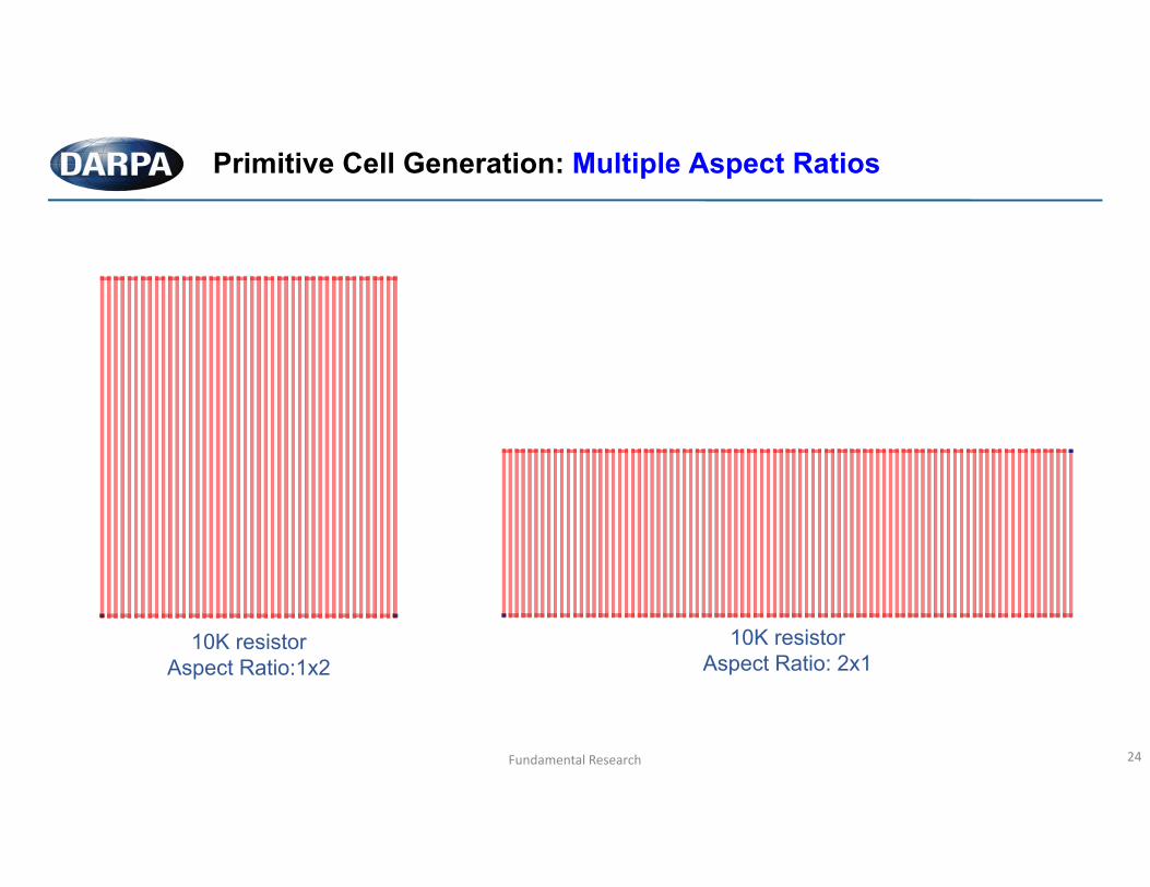
Primitive Cell Generation: Multiple Aspect Ratios
10K resistorAspect Ratio:1x2
10K resistorAspect Ratio: 2x1
Fundamental Research 24

Primitive Cell Generation: Capacitors and Arrays
Unit Capacitor: 10fF 50fF Capacitor ArrayAspect Ratio: 3x2
50fF Capacitor ArrayAspect Ratio: 2x3
Fundamental Research 25

In a bulk technology cells are parameterized by # Fingers, active width, gate length ..
Primitive Cell Generation: Bulk Technology
Lg: Lmin Lg: 4xLminCurrent mirror bank
DA DB
S
4x
DC
G
Fundamental Research 26

The user can specify new primitives by providing:(1) Primitive netlist[pin name, (transistor_name, transistor_node)]Internal pin names not required, denoted by: ‘_’
Primitive Cell Generation: User-specified Primitives
(2) Primitive layout template
[1, S3, (M3, S)], [2, G3, (M3, G)], [3, _, (M1, S), (M2, S), (M3, D)]…
Fundamental Research 27
[D1, (M1, D)][D2, (M2, D)][G1, (M1, G)][G2, (M2, G)][_, (M1, S), (M2, S), (M3, D)][G3, (M3, G)][S3, (M3, S)]
12
.
.
.
.
.3

Fundamental Research 28
Primitives >> sub-blocks >> larger sub-blocks >> system assembly
Incorporates analog constraints at every stage (including constraints “pushed up” from primitives)
Block Assembly, Placement and Routing
PlacementConstraints
…
RoutingConstraints
…Macro Placement
Full Placement
SimulatedAnnealing
Analytical Placement,
Legalization
Global Route
Detailed Route
Candidates Annotation
ILPSelection
Supply Net Routing
Top‐level power grid connected to blocklevel power stripes connected to primitives

Fundamental Research 29
Flexible block assembly for layouts in multi aspect ratiosInput primitives
• Single block schematic• Multiple sets of layouts in different aspect ratios
Output layouts• Different combinations of primitive block layouts• Multiple layouts in different aspect ratios
Block Assembly, Placement and Routing: Multiple Aspect Ratios
Block Assembly
Primitives Final layouts

We have open-sourced (BSD 3-clause license) Intel’s existing internally developed detailed router for analog circuits: https://github.com/ALIGN-analoglayout/AnalogDetailedRouter
Inputs:Grid Abstraction of Process and Design RulesTerminals (Connected Entities)Existing Physical WiresGlobal Routes
Output:Detailed routes connecting at least one terminal from each CE
Approach:Generate multiple candidate routing segments and use SAT to select a set of segments that connects the terminals (for all nets simultaneously) without creating shorts and design rule violations.
Features:Applied to multiple processes within Intel (10, 14, 22FFL, 7, …)Allows different grid templates in different regions of the blockFollows global routes (specifies most analog constraints)Expands global route into multiple detailed tracks (max current)
Intel Analog Detailed Router
Public Release 30

We have open-sourced (BSD 3-clause license) Intel’s existing internally developed detailed router for analog circuits: https://github.com/ALIGN-analoglayout/AnalogDetailedRouter
Inputs:Grid Abstraction of Process and Design RulesTerminals (Connected Entities)Existing Physical WiresGlobal Routes
Output:Detailed routes connecting at least one terminal from each CE
Approach:Generate multiple candidate routing segments and use SAT to select a set of segments that connects the terminals (for all nets simultaneously) without creating shorts and design rule violations.
Features:Applied to multiple processes within Intel (10, 14, 22FFL, 7, …)Allows different grid templates in different regions of the blockFollows global routes (specifies most analog constraints)Expands global route into multiple detailed tracks (max current)
Intel Analog Detailed Router
Public Release 31

We have open-sourced (BSD 3-clause license) Intel’s existing internally developed detailed router for analog circuits: https://github.com/ALIGN-analoglayout/AnalogDetailedRouter
Inputs:Grid Abstraction of Process and Design RulesTerminals (Connected Entities)Existing Physical WiresGlobal Routes
Output:Detailed routes connecting at least one terminal from each CE
Approach:Generate multiple candidate routing segments and use SAT to select a set of segments that connects the terminals (for all nets simultaneously) without creating shorts and design rule violations.
Features:Applied to multiple processes within Intel (10, 14, 22FFL, 7, …)Allows different grid templates in different regions of the blockFollows global routes (specifies most analog constraints)Expands global route into multiple detailed tracks (max current)
Intel Analog Detailed Router
Public Release 32

We have open-sourced (BSD 3-clause license) Intel’s existing internally developed detailed router for analog circuits: https://github.com/ALIGN-analoglayout/AnalogDetailedRouter
Inputs:Grid Abstraction of Process and Design RulesTerminals (Connected Entities)Existing Physical WiresGlobal Routes
Output:Detailed routes connecting at least one terminal from each CE
Approach:Generate multiple candidate routing segments and use SAT to select a set of segments that connects the terminals (for all nets simultaneously) without creating shorts and design rule violations.
Features:Applied to multiple processes within Intel (10, 14, 22FFL, 7, …)Allows different grid templates in different regions of the blockFollows global routes (specifies most analog constraints)Expands global route into multiple detailed tracks (max current)
Intel Analog Detailed Router
Public Release 33

9GHz Phased Array
Fundamental Research 34

Phased Array Receiver: Components
Applications:• mm-Wave communication (5G)• RADAR
Design Blocks:• Low noise amplifier (LNA)• Mixer• Oscillator• Band pass filter (BPF)
Fundamental Research
Phased array receiver block diagram Wideband receiver block diagram
35

TSMC’s 65nm GP CMOS processActive area (excluding test circuits) is 2.7mm2
Phased Array Receiver: Chip Micrograph
Fundamental Research
[ESSCIRC 2018]
36
Hand Crafted

Special PDK Cells (RF transistors, inductors, capacitors, etc.) are characterized and non-gridded.The cells are treated as black box• We make sure that the cell pins are on grids so that our PnR tool can make connections in between the blocks.
Phased Array Receiver: Cell Generation
Fundamental Research 37

Special PDK Cells (RF transistors, inductors, capacitors, etc.) are characterized and non-gridded.The cells are treated as black box• We make sure that the cell pins are on grids so that our PnR tool can make connections in between the blocks.
Phased Array Receiver: Cell Generation
Fundamental Research 38

Special PDK Cells (RF transistors, inductors, capacitors, etc.) are characterized and non-gridded.The cells are treated as black box• We make sure that the cell pins are on grids so that our PnR tool can make connections in between the blocks.
Phased Array Receiver: Cell Generation
Inductor cell from PDK treated as a black boxFundamental Research 39
Grid lines
Grid lines

Special PDK Cells (RF transistors, inductors, capacitors, etc.) are characterized and non-gridded.The cells are treated as black box• We make sure that the cell pins are on grids so that our PnR tool can make connections in between the blocks.
Phased Array Receiver: Cell Generation
Inductor cell from PDK treated as a black boxFundamental Research 40
Grid lines
Grid lines

Band pass filter (BPF)
Phased Array Receiver: Block Layouts
Fundamental Research
BPF schematicHand-Crafted layout
CSCG
41
ALIGN generated layout

ALIGN: General & Extendable
Digitally Controlled Oscillator (DCO): ISSCC 2018 …
Fundamental Research
Proprietary
Proprietary
OPEN-SOURCE
42

ALIGN: General & Extendable
Digitally Controlled Oscillator (DCO): ISSCC 2018 …
Fundamental Research
Proprietary
Proprietary
OPEN-SOURCE
43

Alpha release:
ALIGN: Push Button Layout Compiler
44
Proprietary
Proprietary
OPEN-SOURCE
https://github.com/ALIGN‐analoglayout/ALIGN‐public
Progress since the Jan integration meeting• Global routing/ Detailed routing• Performance analysis• More classes in ML based recognition• Cell generation for RF cells and bulk technologies
DEMO• OTA• Switched-capacitor filter• Wireline equalizer (offline)
Fundamental Research

Any Questions?
45
Switched capacitor filter [Mock FinFET]
Variable gain amplifier [Mock FinFET]
Linear equalizer [Mock FinFET]Switched capacitor filter [ASAP7nm]
Adder [Mock FinFET]Single to differential converter [Mock FinFET]
Bandpass Filter [Bulk 65nm]The views, opinions and/or findings expressed are those of the author and should not be interpreted as representing the official views or policies of
the Department of Defense or the U.S. Government

The views, opinions and/or findings expressed are those of the author and should not be interpreted as representing the official views or policies of the Department of Defense or the U.S. Government.
Fundamental Research 46