ERBE - numlor.fr · Service manual ERBE ICC 200 ICC 300 H-E ICC 350 09.2004
266
Service manual ERBE ICC 200 ICC 300 H-E ICC 350 09.2004
Transcript of ERBE - numlor.fr · Service manual ERBE ICC 200 ICC 300 H-E ICC 350 09.2004
Serv
ice
man
ual
ERBE
ICC 200
ICC 300 H-E
ICC 350
09.2004

ICC 200, ICC 300 H-E, ICC 350
SERVICE MANUAL
09.2004
10128-002, 10128-009, 10128-010, 10128-015, 10128-016
10128-023, 10128-025, 10128-027, 10128-028, 10128-036
10128-051, 10128-054, 10128-055, 10128-056, 10128-058
10128-061, 10128-064, 10128-065, 10128-066, 10128-070
10128-071, 10128-072, 10128-073, 10128-074, 10128-075
10128-076, 10128-077, 10128-078, 10128-080, 10128-081
10128-082, 10128-083, 10128-200, 10128-202, 10128-204
10128-205, 10128-206, 10128-213, 10128-214, 10128-300
10128-301, 10128-303, 10128-304, 10128-305, 10128-306
10128-307,10128-310, 10128-403

All rights to this service manual, particularly the right to reproduction, distribution and translation,are reserved. No part of this service manual may be reproduced in any form (including photocopying,microfilm or other means), or processed, reproduced or distributed by means of electronic systemswithout prior written permission from ERBE Elektromedizin GmbH.
The information contained in this service manual may be revised or extended without prior noticeand represents no obligation on the part of ERBE Elektromedizin GmbH.
Copyright © ERBE Elektromedizin GmbH, Tübingen 2004
Printed by: ERBE Elektromedizin GmbH, Tübingen Art. No.: 80116-201
Printed in Germany
Please contact me directly with yoursuggestions, criticism or informationregarding this manual. Your feedbackhelps me design this documentaccording to your requirements and toconstantly improve it.
This service manual was created by
Michael GrosseDipl.-Phys. (Physicist)
Tel (+49) 70 71 / 755–254Fax (+49) 70 71 / 755–5254E-Mail [email protected]
Net http://www.erbe-med.de
5 / 266
Art.
No.
: 801
16-2
0109
/ 2
004
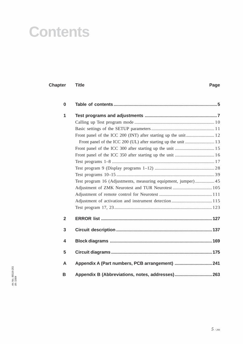
Contents
Chapter Title Page
0 Table of contents ...................................................................................5
1 Test programs and adjustments ..........................................................7Calling up Test program mode ....................................................................... 10
Basic settings of the SETUP parameters ........................................................ 11
Front panel of the ICC 200 (INT) after starting up the unit ......................... 12
Front panel of the ICC 200 (UL) after starting up the unit .......................... 13
Front panel of the ICC 300 after starting up the unit ................................... 15
Front panel of the ICC 350 after starting up the unit ................................... 16
Test programs 1–8 ........................................................................................... 17
Test program 9 (Display programs 1–12) ..................................................... 28
Test programs 10–15 ....................................................................................... 39
Test program 16 (Adjustments, measuring equipment, jumper) ................. 45
Adjustment of ZMK Neurotest and TUR Neurotest ................................... 105
Adjustment of remote control for Neurotest ............................................... 111
Adjustment of activation and instrument detection .................................... 115
Test program 17, 23 ....................................................................................... 123
2 ERROR list ......................................................................................... 127
3 Circuit description .............................................................................137
4 Block diagrams .................................................................................. 169
5 Circuit diagrams ................................................................................. 175
A Appendix A (Part numbers, PCB arrangement) .............................. 241
B Appendix B (Abbreviations, notes, addresses) .............................. 263

6 / 266

Chapter 1Test programsand
adjustments


1 TEST PROGRAMS AND ADJUSTMENTS 9 / 266
Art
. No.
: 801
16-2
0109
/ 20
04
Test programsERBOTOM ICC 350, 300, 200Version 4.0 / 3.0 / 2.0
No. Test program function V 4.0 / 3.0 / V 2.0
1 Basic front panel setting (only ICC 300 and 200) x
2 Calls up the Error list x
3 Test of all D-flipflop circuit memories x
4 Test of all front panel visual signals x
5 Test of all acoustic signals x
6 Test of all relays x
7 NESSY: Version number setting x
8 Display of software version no. and option no. x
9 Activation of display programs x
10 Time limit setup x
11Measurement and display of extra-low voltages +15 volts, –15 volts,+24 volts and the temperature
x
12 Setting the FORCED voltage (2.0: 3 x forced; 4.0: 4 x forced) x
13 not assigned
14 not assigned
15 not assigned
16 Test and setting help for all unit calibration functions x
17 Brightness setting for the seven-segment displays x
18 not assigned
19 not assigned
20 not assigned
21 not assigned
22 not assigned
23 AUTO START start delay setup x

1 TEST PROGRAMS AND ADJUSTMENTS10 / 266
Calling up theTEST PROGRAM mode
Note regarding the drawing
The front panel shown of the ICC 350 applies to the ICC 200 and ICC 300 in such a way that only theAUTO CUT and AUTO COAG control panels apply to the ICC 300, and the AUTO CUT, AUTO COAGand AUTO BIPOLAR control panels apply to the ICC 300.
Calling up
Press key 3 (Roll) when switching on the power and hold it down.
Setting the test program number
Using keys 8 (Up) or 9 (Down), set the required program number.
Starting and finishing test programs
By pressing key 3 (Roll), start or finish a test program.
Exiting the test program mode
Exit the TEST PROGRAM MODE by switching off the power or setting TEST PROGRAM no. 0 using key 9(Down).
4 1185 9 12 1573 16
�� ���� ���� ���� � � ���
1 2
14
1 TEST PROGRAMS AND ADJUSTMENTS 11 / 266
Art
. No.
: 801
16-2
0109
/ 20
04
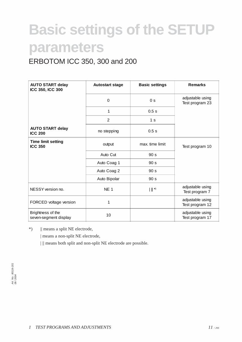
Basic settings of the SETUPparametersERBOTOM ICC 350, 300 and 200
*) || means a split NE electrode,
| means a non-split NE electrode,
| || means both split and non-split NE electrode are possible.
AUTO START delayICC 350, ICC 300
Autostart stage Basic settings Remarks
0 0 sadjustable usingTest program 23
1 0.5 s
2 1 s
AUTO START delayICC 200 no stepping 0.5 s
Time limit settingICC 350 output max. time limit Test program 10
Auto Cut 90 s
Auto Coag 1 90 s
Auto Coag 2 90 s
Auto Bipolar 90 s
NESSY version no. NE 1 | || *) adjustable usingTest program 7
FORCED voltage version 1adjustable usingTest program 12
Brightness of theseven-segment display
10adjustable usingTest program 17
1 TEST PROGRAMS AND ADJUSTMENTS12 / 266
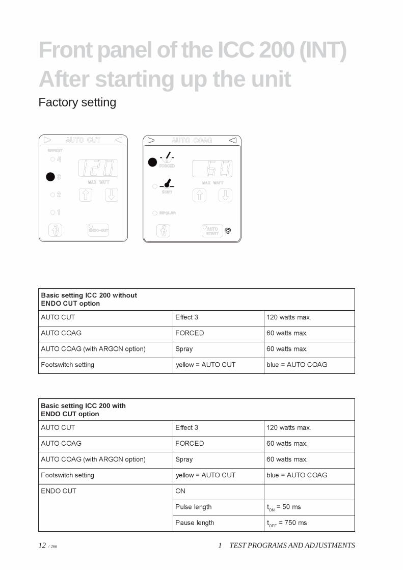
Front panel of the ICC 200 (INT)After starting up the unitFactory setting
��������������� ������������������
������� ���� � ����������
�������� ������ � ���������
������������ ���!�������� "�#�$ � ���������
%����� ��������� �������&��''" ��������&(')
htiw002CCIgnittescisaBnoitpoTUCODNE
������� ���� � ����������
�������� ������ � ���������
������������ ���!�������� "�#�$ � ���������
%����� ��������� �������&��''" ��������&(')
������� ��
�%�'�'(* � �� ���+&
�%�'�(�* � ��� ���+,&
1 TEST PROGRAMS AND ADJUSTMENTS 13 / 266
Art.
No.
: 801
16-2
0109
/ 20
04
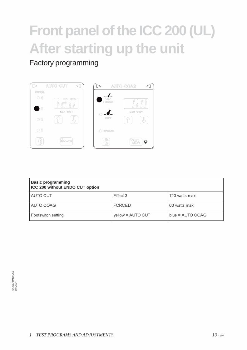
Front panel of the ICC 200 (UL)After starting up the unitFactory programming
gnimmargorpcisaBnoitpoTUCODNEtuohtiw002CCI
������� ���� � ����������
�������� ������ � ���������
%����� ��������� �������&��''" ��������&(')
1 TEST PROGRAMS AND ADJUSTMENTS14 / 266
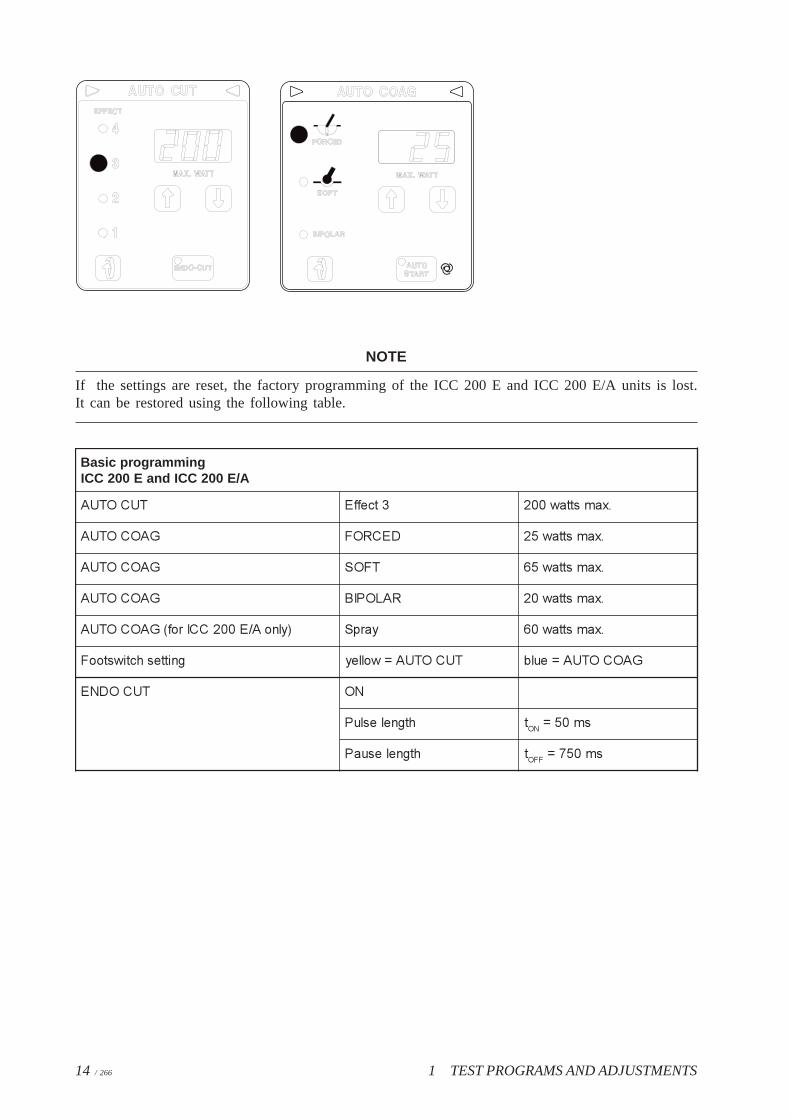
NOTE
If the settings are reset, the factory programming of the ICC 200 E and ICC 200 E/A units is lost.It can be restored using the following table.
gnimmargorpcisaBA/E002CCIdnaE002CCI
������� ���� � ����������
�������� ������ � �������+�
�������� ���$ � �������+�
�������� ��-�*./ � ���������
�"'���0������.#�!�������� "�#�$ � ���������
%����� ��������� �������&��''" ��������&(')
������� ��
�%�'�'(* � �� ���+&
�%�'�(�* � ��� ���+,&
1 TEST PROGRAMS AND ADJUSTMENTS 15 / 266
Art
. No.
: 801
16-2
0109
/ 20
04
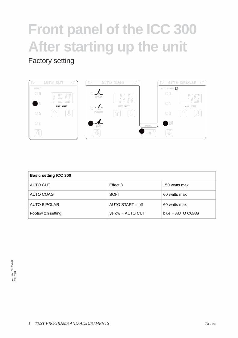
Front panel of the ICC 300After starting up the unitFactory setting
Basic setting ICC 300
AUTO CUT Effect 3 150 watts max.
AUTO COAG SOFT 60 watts max.
AUTO BIPOLAR AUTO START = off 60 watts max.
Footswitch setting yellow = AUTO CUT blue = AUTO COAG
1 TEST PROGRAMS AND ADJUSTMENTS16 / 266
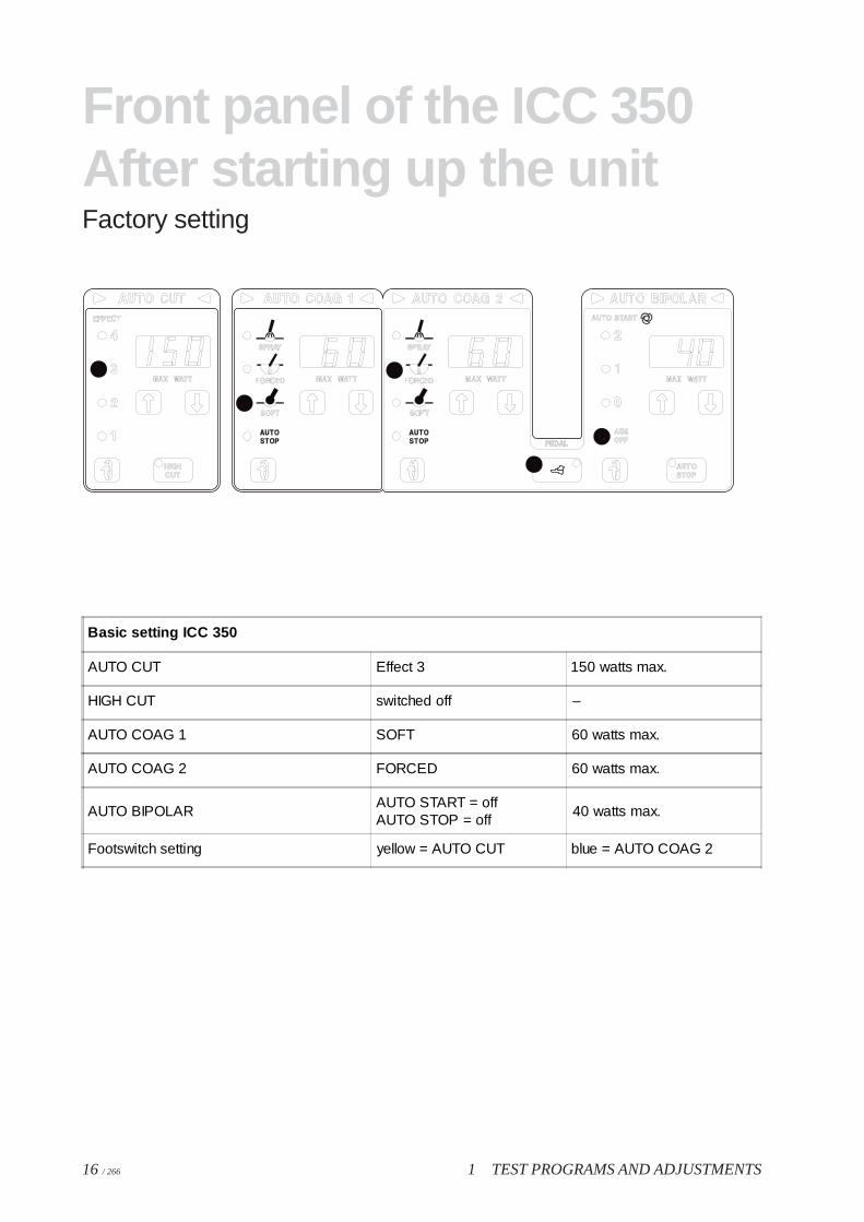
Front panel of the ICC 350After starting up the unitFactory setting
Basic setting ICC 350
AUTO CUT Effect 3 150 watts max.
HIGH CUT switched off –
AUTO COAG 1 SOFT 60 watts max.
AUTO COAG 2 FORCED 60 watts max.
AUTO BIPOLARAUTO START = offAUTO STOP = off
40 watts max.
Footswitch setting yellow = AUTO CUT blue = AUTO COAG 2

1 TEST PROGRAMS AND ADJUSTMENTS 17 / 266
Art
. No.
: 801
16-2
0109
/ 2
004
Test program no. 1ICC 200, 300 only
General description
Using this test program, any front panel setting can be made. This setting is known as the basic setting.After termination, the basic setting is stored internally. Only completely saved channels are stored. Thebasic setting display flashes. Acknowledge by pressing any key.
Termination
Using “Power off”.
Switch off a channel
Using the “Down” key (8), set the lowest intensity. Once the lowest display is set, the seven-segmentdisplay changes to “---”. This means that the channel has been switched off.
Basic setting and brief power failure
For a brief power failure of 15 seconds max., the front panel setting last set is displayed.
Activation of a channel is blocked if a channel has not been completely set or the basic setting was notacknowledged.
The basic setting set at the factory corresponds to the FIXE basic setting.
FIXE basic setting
A FIXE basic setting is stored in the program. This basic setting is accepted and displayed if:
• the stored front panel setting is invalid, e.g. through failure of the circuit memory or through batterymemory lost,
• in Test program 1, the “All off” setting has been accepted.

1 TEST PROGRAMS AND ADJUSTMENTS18 / 266
Test program no. 2Call up and display of the error memory
General description
The ICC units are equipped with a system for error detection, error indication and error memory. Every errorreceives an error number (ERROR no.). The unit stores the last 10 ERROR numbers. Test program 2 displaysthe stored ERROR numbers. The most recent error occurring chronologically is in memory location 1.
Display
AUTO CUT AUTO COAG 1 AUTO COAG 2 AUTO BIPOLAR
Err. 1 ... 10 xxx
xxx: Display of the error number
By pressing keys 8 (Up) or 9 (Down), you can call up the memory locations one after another. By pressingkey 7, you delete the error numbers at all memory locations.
Example
After starting the test program with key 3, for example, Error no. 2 appears at memory location 1 with thefollowing display:
Display
AUTO CUT AUTO COAG 1 AUTO COAG 2 AUTO BIPOLAR
Err. 1 2

1 TEST PROGRAMS AND ADJUSTMENTS 19 / 266
Art
. No.
: 801
16-2
0109
/ 20
04
Test program no. 3Test of all D-flipflop circuit memories
*) buS is the seven-segment display for the word „BUS“.
General description
Test of all D-flipflop (D-FF) circuit memories. After starting the test with key 3, you will see the following display:
Display(ICC 350, ICC 300)
AUTO CUT AUTO COAG 1 AUTO COAG 2 AUTO BIPOLAR
buS *) 0 d0 ... d7 alternating
Display(ICC 200)
buS d0 ... d7 alternating
buS*) (D-FF-Test Nr. 0) tests the external control bus for signal lines d0–d7. The signal lines d0–d7 areswitched on and off one after another. The switching statuses can be displayed on the bar graph (adapterboard 30183-102).
Using the keys 8 (Up) or 9 (Down), you can call up D-FF tests 1-11. You will see the following display:
Display(ICC 350, ICC 300)
AUTO CUT AUTO COAG 1 AUTO COAG 2 AUTO BIPOLAR
dFF 1 ... 11 d0 ... d7 alternating
Display(ICC 200)
dFF 1 ... 9 d0 ... d7 alternating
The D-FF signal lines d0-d7 are switched on and off one after another. The signals can be measured at theD-FF outputs. There is an error if
• there is more than one output status at the same time,
• there is constantly an output signal in spite of switching over,
• there is no output signal in spite of D-FF activation.

1 TEST PROGRAMS AND ADJUSTMENTS20 / 266
Overview of the D-flipflop tests
Test no. D-FF description Position Remarks
0 external control bus Motherboard
1 D-FF IC 2 Motherboard
2 D-FF IC 3 Motherboard
3 D-FF IC 9 Extra-low voltage and tone
4 D-FF IC 19 Control board
5 D-FF IC 20 Control board
6 D-FF IC 6 ST power stage
7 D-FF IC 10 Senso-board
8 D-FF IC 8 Relay board not ICC 200
9 Extension motherboard slot J9 not ICC 200
10 Extension motherboard slot J9 not ICC 200
11 Extension motherboard slot J9 not ICC 200
Test program no. 3Test of all D-flipflop circuit memories

1 TEST PROGRAMS AND ADJUSTMENTS 21 / 266
Art
. No.
: 801
16-2
0109
/ 20
04
Test program no. 4Check of the optical signals on the frontpanel
General description
Using this program, you can test the optical displays on the front panel. After starting the test program, youwill see the following display:
All optical signals on the front panel are switched on. The 7-segment displays show “8.” for all numbers.
1 TEST PROGRAMS AND ADJUSTMENTS22 / 266
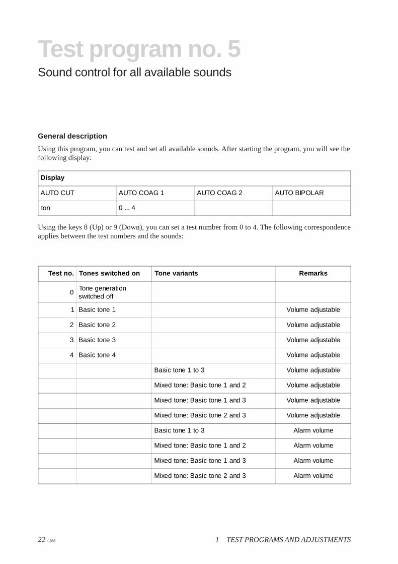
Test program no. 5Sound control for all available sounds
General description
Using this program, you can test and set all available sounds. After starting the program, you will see thefollowing display:
Display
AUTO CUT AUTO COAG 1 AUTO COAG 2 AUTO BIPOLAR
ton 0 ... 4
Using the keys 8 (Up) or 9 (Down), you can set a test number from 0 to 4. The following correspondenceapplies between the test numbers and the sounds:
Test no. Tones switched on Tone variants Remarks
0Tone generationswitched off
1 Basic tone 1 Volume adjustable
2 Basic tone 2 Volume adjustable
3 Basic tone 3 Volume adjustable
4 Basic tone 4 Volume adjustable
Basic tone 1 to 3 Volume adjustable
Mixed tone: Basic tone 1 and 2 Volume adjustable
Mixed tone: Basic tone 1 and 3 Volume adjustable
Mixed tone: Basic tone 2 and 3 Volume adjustable
Basic tone 1 to 3 Alarm volume
Mixed tone: Basic tone 1 and 2 Alarm volume
Mixed tone: Basic tone 1 and 3 Alarm volume
Mixed tone: Basic tone 2 and 3 Alarm volume

1 TEST PROGRAMS AND ADJUSTMENTS 23 / 266
Art
. No.
: 801
16-2
0109
/ 20
04
Test program no. 5Sound control for all available sounds
Frequency adjustment for warning tones
The warning tone frequency setting can be adjusted independently of other assemblies on the low-voltagepower supply (jumper J2) with Test program no. 5.
• Activate Test program no. 5. MP 4 is GND for frequency counter.
• Call »Tone 1«: Set frequency at MP 1 with TP 2 to 493 Hz (±2 Hz) with frequency counter.
• Call »Tone 2«: Set frequency at MP 2 with TP 3 to 414 Hz (±2 Hz) with frequency counter.
• Call »Tone 3«: Set frequency at MP 3 with TP 4 to 329 Hz (±2 Hz) with frequency counter.
• To check settings the various tones and mixed tones are generated one after the other by calling»Tone 4«. Here, take especial care that the operating and warning tones have different volumes.

1 TEST PROGRAMS AND ADJUSTMENTS24 / 266
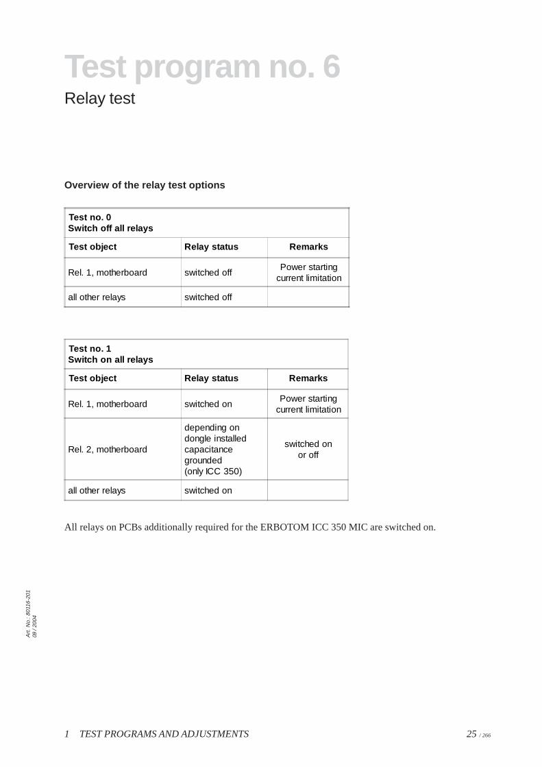
Test program no. 6Relay test
General description
Using this program, all relays can be actuated. The NESSY measurement monitor is switched off. Afterending the test program, relay no. 1 is switched on for the power starting current limitation.
Test program no. 6 is also intended for safety testing of the unit. With this test, there may be a brieffailure of the power supply due to the external intervention. If the test program is activated, the testprogram is automatically called up again after a brief power failure of up to approx. 15 seconds. However,if the power failure is longer than 15 seconds, this will not occur.
After starting the test program, you will see the following display:
Display
AUTO CUT AUTO COAG 1 AUTO COAG 2 AUTO BIPOLAR
rEL 0 ... 1
Designation of the PCBs with their assigned relays
PCB Slot Relay function Remarks
Motherboard ICC 350 – see lines 3 and 4
Motherboard ICC 200 – see lines 3 and 4
Motherboard – Rel. 1: Power starting current limitation
Motherboard – Rel. 2: Capacitance ground only for ICC 350
Power module J5 Rel. 1: Switchover ST generator: HF
ST power stage J6 Rel. 1: Output HF: UE1 to NE
ST power stage J6 Rel. 2: Output HF: Rel. 3 to AE
ST power stage J6 Rel. 3: Output HF: UE1 to AE
ST power stage J6 Rel. 19: Connection to power supply
Senso-board J7 Rel. 1: Output NE - NESSY
Senso-board J7 Rel. 2: Output AE
Senso-board J7 Rel. 3: Output NE
Relay board J8 Rel. 1: Output AE 1 only ICC 300 / 350
Relay board J8 Rel. 2: Output AE 2 only ICC 300 / 350
ICC 200: Mono outputboard
J8 Rel. 1: Output AE 1 only ICC 200
1 TEST PROGRAMS AND ADJUSTMENTS 25 / 266
Art
. No.
: 801
16-2
0109
/ 20
04
Overview of the relay test options
Test no. 0Switch off all relays
Test object Relay status Remarks
Rel. 1, motherboard switched offPower starting
current limitation
all other relays switched off
Test no. 1Switch on all relays
Test object Relay status Remarks
Rel. 1, motherboard switched onPower starting
current limitation
Rel. 2, motherboard
depending ondongle installedcapacitancegrounded(only ICC 350)
switched onor off
all other relays switched on
All relays on PCBs additionally required for the ERBOTOM ICC 350 MIC are switched on.
Test program no. 6Relay test

1 TEST PROGRAMS AND ADJUSTMENTS26 / 266
Test program no. 7Setting the NESSY version
General description
Using this program, you can set four NESSY versions. After starting the test program, you will see thefollowing displays when you activate key 3:
Display
AUTO CUT AUTO COAG 1 AUTO COAG 2 AUTO BIPOLAR
NE.1 || or |
In the AUTO COAG field:
|| means a split neutral electrode,
| means of non-split neutral electrode.
Using the keys 8 (Up) or 9 (Down), you can set four different NESSY versions:
No. AUTO CUT AUTO COAG 1 Remarks
1 NE.1 || or | for split and non-split electrodes
2 NE.2 | only for non-split electrodes
3 NE.3 ||only for split electrodes; acoustic (3 times) and
visual alarm
4 NE.4 ||only for split electrodes; acoustic (continuous
tone) and visual alarm
At the end of the test, the NESSY version number is stored. Version number 1 is the standard version setwhen the unit is delivered. In case of memory failure, version no. 1 is automatically set. When switching onthe power, version no. 2, 3 or 4 is displayed briefly if this is set. The standard version no. 1 is not displayed.

1 TEST PROGRAMS AND ADJUSTMENTS 27 / 266
Art
. No.
: 801
16-2
0109
/ 20
04
Test program no. 8Display of the software version and anyoptions
General description
Using this program, you can display the software version, while on the ICC 350 and ICC 300, you can alsosee the display of an option identification number.
After starting the program, you will see the following display:
Display
AUTO CUT AUTO COAG 1 AUTO COAG 2 AUTO BIPOLAR
Snr x.xx y
Explanation:
x.xx Software version no. (e.g. 2.0)
y Option code no. (e.g. 8).
Codeno. means
0 Unit without option
1 ICC 350: Neurotest ZMK
2 ICC 350: Neurotest TUR
4
8 ICC 350: ENDO CUT function
16
32
64
128
256
The code number is based on a binary code:
Example
Code no. 2 means ICC 350 Neurotest TUR
Code no. 9 means ICC 350 Neurotest ZMK + Endocut
1 + 8

1 TEST PROGRAMS AND ADJUSTMENTS28 / 266
Test program no. 9Activating display programs to displaymeasurement values
General description
This program activates displays in the standby mode or during activation. With key 3, Test program no. 9 isstarted.
After starting, you will see the following display:
Display
AUTO CUT AUTO COAG 1 AUTO COAG 2 AUTO BIPOLAR
nr. 0
Within Test program no. 9, 22 subprograms for displaying specific data can be called up, while subprograms16 to 22 are intended only for use by the manufacturer.
These subprograms can now be set using keys 8 (Up) or 9 (Down). Once the required display program hasbeen selected, it is reactivated using key 3. The selected display program remains activated until the poweris switched off.
Display
AUTO CUT AUTO COAG 1 AUTO COAG 2 AUTO BIPOLAR
nr. 0 ... 22

1 TEST PROGRAMS AND ADJUSTMENTS 29 / 266
Art
. No.
: 801
16-2
0109
/ 20
04
Display programs nos. 1–3
The selected display program now displays the required data during regular operation of the unit. To dothis, the appropriate operating modes must be set and the accessories activated.
The display program remains activated until the power is switched off. To return to normal operation, theunit must be switched off for a short time and switched back on again.
Display program no. 1: not assigned
Display program no. 2: not assigned
Display program no. 3:
ST generator time control with activation of SPRAY or FORCED.
Display for ICC 350 and ICC 300:
AUTO CUT AUTO COAG 1 AUTO COAG 2 AUTO BIPOLAR
ttt P 2 P 3 tst
ttt Difference between set frequency and actual frequency
P 2 Set power [W]
P 3 Set power [W]
tst Abbreviation of the test title (Time-ST stage)
Display program no. 3:
ST generator time control with activation of FORCED.
Display on ICC 200:
AUTO CUT AUTO COAG
ttt tst
ttt Difference between set frequency and actual frequency
tst Abbreviation of the test title (Time-ST stage)
1 TEST PROGRAMS AND ADJUSTMENTS30 / 266
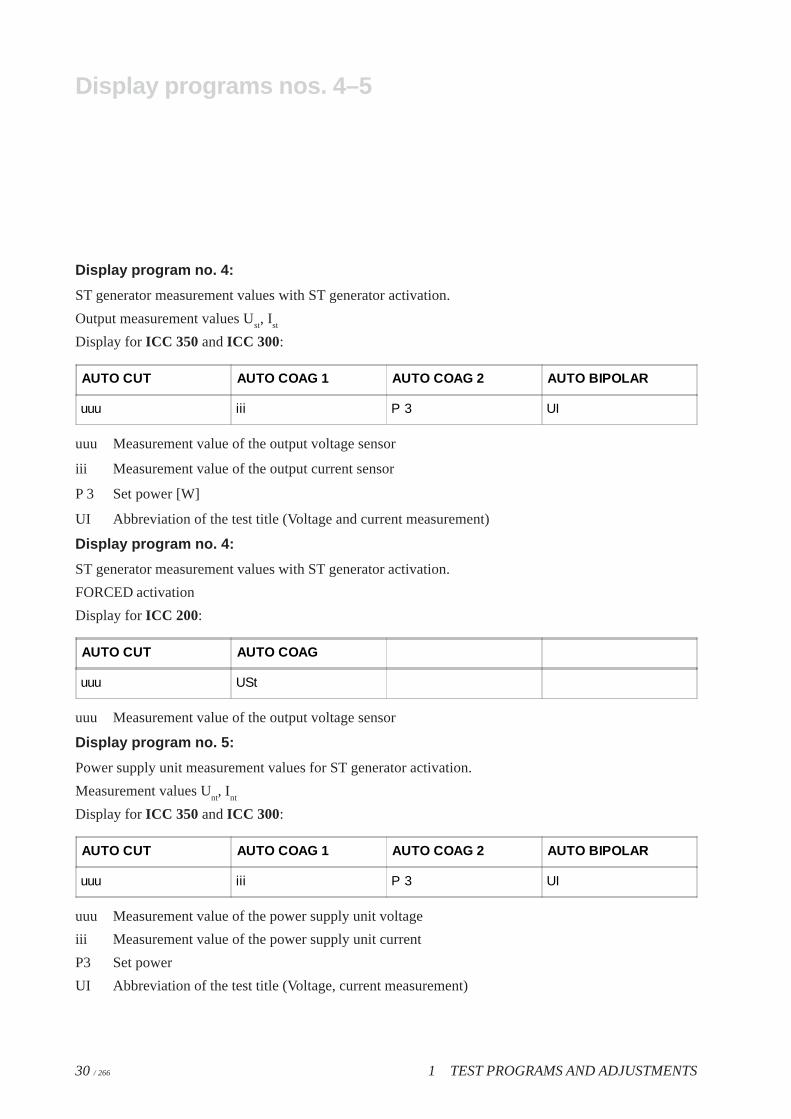
Display program no. 4:
ST generator measurement values with ST generator activation.
Output measurement values Ust, I
st
Display for ICC 350 and ICC 300:
AUTO CUT AUTO COAG 1 AUTO COAG 2 AUTO BIPOLAR
uuu iii P 3 UI
uuu Measurement value of the output voltage sensor
iii Measurement value of the output current sensor
P 3 Set power [W]
UI Abbreviation of the test title (Voltage and current measurement)
Display program no. 4:
ST generator measurement values with ST generator activation.
FORCED activation
Display for ICC 200:
AUTO CUT AUTO COAG
uuu USt
uuu Measurement value of the output voltage sensor
Display program no. 5:
Power supply unit measurement values for ST generator activation.
Measurement values Unt, I
nt
Display for ICC 350 and ICC 300:
AUTO CUT AUTO COAG 1 AUTO COAG 2 AUTO BIPOLAR
uuu iii P 3 UI
uuu Measurement value of the power supply unit voltage
iii Measurement value of the power supply unit current
P3 Set power
UI Abbreviation of the test title (Voltage, current measurement)
Display programs nos. 4–5

1 TEST PROGRAMS AND ADJUSTMENTS 31 / 266
Art
. No.
: 801
16-2
0109
/ 20
04
Display program no. 5:
Power supply measurement values with ST generator activation, FORCED activation.
Measurement values Unt, I
nt
Display for ICC 200:
AUTO CUT AUTO COAG
uuu Unt
uuu Measurement value of the power supply unit voltage
Display program no. 6:
ST generator measurement values for ST generator activation, FORCED activation.
Measurement value Ist
Display for ICC 200:
AUTO CUT AUTO COAG
iii Ist
iii Measurement value of the output current sensor
Display program no. 7:
Power supply unit measurement values for ST generator activation, FORCED activation.
Measurement value Int
Display for ICC 200:
AUTO CUT AUTO COAG
iii Int
iii Measurement value of the power supply unit current
Display program nos. 5–7
1 TEST PROGRAMS AND ADJUSTMENTS32 / 266
Display program no. 8:
Measurement values for activation of the sine-wave generator.
AUTO CUT, AUTO COAG 1 and 2 in SOFT mode, AUTO BIPOLAR
Output measurement value Uact
Display for ICC 350 and ICC 300:
AUTO CUT AUTO COAG 1 AUTO COAG 2 AUTO BIPOLAR
ppp uuu cos PU
ppp HF power output [W], present power output
uuu HF output voltage [V], present output voltage
cos cos-j-value from the table (ICC 350 only)
PU Abbreviation of the test title (Power and voltage measurement)
Display program no. 8
Display program no. 8:
Measurement values for activation of the sine-wave generator.
AUTO CUT, AUTO COAG 1 and 2 in SOFT mode, AUTO BIPOLAR
Output measurement value Uact
Display for ICC 200:
AUTO CUT AUTO COAG
ppp P
ppp HF power output [W]
P Abbreviation of the test title (Power measurement)

1 TEST PROGRAMS AND ADJUSTMENTS 33 / 266
Art
. No.
: 801
16-2
0109
/ 20
04
Display program no. 9:
Measurement values for activation of the sine-wave generator.
AUTO CUT, AUTO COAG 1 and 2 in SOFT mode, AUTO BIPOLAR
Output measurement values Ireal
, cos j (Real part of the current and cos j between voltage and current)
Display for ICC 350 and ICC 300:
AUTO CUT AUTO COAG 1 AUTO COAG 2 AUTO BIPOLAR
iii cos ppp IC
iii Real part of the measurement value from the HF output current
cos cos-j value from the table (ICC 350 only)
ppp HF power output [W] for ICC 350
IC Abbreviation of the test title (Current measurement and cos j measurement)
Display program no. 9:
Measurement values for activation of the sine-wave generator.
AUTO CUT, AUTO COAG 1 and 2 in SOFT mode, AUTO BIPOLAR
Output measurement value: Measurement value of the real part of the HF output current
Display for the ICC 200:
AUTO CUT AUTO COAG
iii I
iii Measurement value of the real part of the HF output current
I Abbreviation of the test title (Current measurement)
Display program no. 9
1 TEST PROGRAMS AND ADJUSTMENTS34 / 266
Display program no. 10:
Measurement values for activation of the sine-wave generator.
AUTO CUT, AUTO COAG 1 and 2 in SOFT mode, AUTO BIPOLAR
Output measurement value Uact
Display for the ICC 200:
AUTO CUT AUTO COAG
uuu U
uuu HF output voltage [V]
U Abbreviation of the test title (Voltage measurement)
Display program no. 11:
Measurement values for activation of the sine-wave generator.
AUTO CUT, AUTO COAG 1 and 2 in SOFT mode, AUTO BIPOLAR
Output measurement value cos j
Display for the ICC 200:
AUTO CUT AUTO COAG
cos Cos
cos cos-j value from the table
Cos Abbreviation of the test title (cos-j measurement)
Display programs nos. 10–11
1 TEST PROGRAMS AND ADJUSTMENTS 35 / 266
Art
. No.
: 801
16-2
0109
/ 20
04
Display program no. 12 (Start)
Display program no. 12:
Contact resistance at AUTO START, in standby operation.
Only valid for AUTO START 0, 1, 2 and in standby operation.
Display for ICC 350 and ICC 300:
AUTO CUT AUTO COAG 1 AUTO COAG 2 AUTO BIPOLAR
uuu P2 P3 br
uuu Measurement value of the contact monitor voltage measurement
P2 Set power for AUTO COAG 1 [W]
P3 Set power for AUTO COAG 2 [W]
br Contact monitor
Display program no. 12:
Contact resistance for AUTO START, in active condition.
Only valid for AUTO START 0, 1, 2 and in active condition.
Display for ICC 350 and ICC 300:
AUTO CUT AUTO COAG 1 AUTO COAG 2 AUTO BIPOLAR
rda P2 P3 br
rda Calculated value of the contact resistance [ohms]
P2 Set power for AUTO COAG 1 [W]
P3 Set power for AUTO COAG 2 [W]
br Contact monitor
1 TEST PROGRAMS AND ADJUSTMENTS36 / 266
Display program no. 12 (continued)
Display program no. 12:
Contact resistance for AUTO START, in standby operation.
Display for ICC 200:
AUTO CUT AUTO COAG
uuu br
uuu Measurement value of the contact monitor voltage measurement
br Contact monitor
Display program no. 12:
Contact resistance for AUTO START, in active condition.
Display for ICC 200:
AUTO CUT AUTO COAG
rda br
rda Calculated value of the contact resistance [ohms]
br Contact monitor
1 TEST PROGRAMS AND ADJUSTMENTS 37 / 266
Art
. No.
: 801
16-2
0109
/ 20
04
Display program no. 15:
NESSY transition resistance in stand-by-operation and on activation.
Display for ICC 350 and ICC 300:
AUTO CUT AUTO COAG 1 AUTO COAG 2 AUTO BIPOLAR
rtr P2 P3 br
rtr calculated NESSY transition resistance [Ohm]
P2 set power for AUTO COAG 1 [W]
P3 set power for AUTO COAG 2 [W]
br AUTO START monitor
Display program no. 15:
NESSY transition resistance in stand-by-operation and on activation.
Display for ICC 200:
AUTO CUT AUTO COAG
rtr r
rtr calculated NESSY transition resistance [Ohm]
r AUTO START monitor
Display program no. 15

1 TEST PROGRAMS AND ADJUSTMENTS38 / 266
NOTE
Display programs nos. 13 and 14 are not assigned. The program nos. 17–22 are only intended for internaluse by the manufacturer.
Display programs nos. 13–22

1 TEST PROGRAMS AND ADJUSTMENTS 39 / 266
Art
. No.
: 801
16-2
0109
/ 20
04
Test program no. 10Changing the maximum time limit
General description
Using this program, you can change the time limit for the ICC 200, 300 and 350. The setting range variesfrom 3 to 960 seconds.
Using the appropriate “Up” or “Down” keys, the time limit restriction for every current quality can be setindividually.
For the ICC 350, various time limit settings can be stored in the individual program memories for each user.This occurs after selecting the program number with program memory key 2 and then changing the respectivecurrent qualities using the appropriate “Up” or “Down” key.
After termination of Test program 10 using key 3, the settings made are stored.
In case of memory failure, as well as in the delivery condition, the max. time limit for all programs andcurrent qualities (CUT, COAG 1, COAG 2, BIPOLAR) is set at 90 seconds.
After starting Test program 10 with key 3, you will see the following display:
AUTO CUT AUTO COAG 1 AUTO COAG 2 AUTO BIPOLAR
t1 t2 t3 t4
• t1: Time limit restriction for AUTO CUT in seconds
• t2: Time limit restriction for AUTO COAG 1 in seconds
• t3: Time limit restriction for AUTO COAG 2 in seconds
• t4: Time limit restriction for AUTO BIPOPLAR in seconds.
Using the following keys, you can adjust the max. time limit (see page 1-4):
• AUTO CUT : Keys 4 and 5
• AUTO COAG 1 : Keys 8 and 9
• AUTO COAG 2 : Keys 11 and 12
• AUTO BIPOLAR: Keys 15 and 16

1 TEST PROGRAMS AND ADJUSTMENTS40 / 266
Test program no. 11Measurement value output for themeasurement channels
Using this program, you can measure the internal supply voltages and the temperature of the unit. In addition,you can display all analog direct measurement channels 1, 2, 3 and 4 as well as analog multiplex measurementchannels.
After starting the test program, you will see the following display:
Display ICC 350 / 300
AUTO CUT AUTO COAG 1 AUTO COAG 2 AUTO BIPOLAR
U 0 XX.X
U– 1 XX.X
U 2 XX.X
tPt ttt xxx
Ch 4 … 22 yyy
• XX.X Voltage value [V]
• ttt Temperature [°C]
• xxx ADC measurement value in the range 0 … 255
• yyy ADC measurement value in the range 0 … 255
Using the keys “Up” (8) or “Down” (9), call up the subprograms U, U-, tPt and Ch 4 … 22.
U0 is the low voltage controlled to +15 volts ±10%
U–1 is the low voltage controlled to –15 volts ±10%
U2 is the low voltage controlled to 24 volts ±10%
tPt is the temperature display of the output stage ±15%
Ch4 … 22 are the analog measurement channels according to the following table:
Display ICC 200
AUTO CUT AUTO COAG 1 AUTO COAG 2 AUTO BIPOLAR
U.15 XX.X
–15 XX.X
U.24 XX.X
tPt ttt
C.aa yyy
1 TEST PROGRAMS AND ADJUSTMENTS 41 / 266
Art
. No.
: 801
16-2
0109
/ 20
04
• XX.X Voltage rating [ V ]
• ttt Temperature [°C ]
• C.aa Channel number
• yyy ADC measurement value in the range 0 ... 255
Using the “Up” (8) or “Down” (9) keys, call up the subprograms U, U-, tPt und C. 4-22.
U0 is the supply voltage controlled to +15 volts
U–1 is the supply voltage controlled to –15 volts
U2 is the supply voltage controlled to +24 volts
tPt is the temperature display of the output stage
C. 4 … 22 are the analog measurement channels according to the following table.
Voltage test U 0 or U.15
Measurement and display of the supply voltage controlled to +15 volts
Display XX.X: e.g. 14.6 equals 14.6 volts
Voltage test U–1 or –15
Measurement and display of the supply voltage controlled to –15 volts
Display XX.X: e.g. 14.6 equals –14.6 volts
Voltage test U 2 or U.24
Measurement and display of the supply voltage controlled to +24 volts
Display XX.X: e.g. 23.6 equals +23.6 volts
Measurement of the output stage temperature
Display tPt 25 means that the temperature inside the unit is 25 °C.
Test of the analog measurement channels (Subtest 4 … 22)
Measurement and display of 19 analog measurement channels inside the unit.
(Intended for internal use by the manufacturer only).
Test program no. 11Measurement value output of themeasurement channels

1 TEST PROGRAMS AND ADJUSTMENTS42 / 266

1 TEST PROGRAMS AND ADJUSTMENTS 43 / 266
Art
. No.
: 801
16-2
0109
/ 20
04
Test program no. 12Setting the FORCED voltage
General description
When this program is called up, the set FORCED version is displayed. Using the “Up” (8) or “Down” (9)keys, you can set one of three (V2.0) or four (V4.0) FORCED versions.
With FORCED coagulation, the ST pulse generator produces short pulses with a high no-load voltage. Thehigh no-load voltage has both advantages and disadvantages which are described in this section with thefeatures.
Using Test program 12, the no-load voltage can be changed relative to the set power limitation.
After starting the test program, you will see the following display:
AUTO CUT AUTO COAG 1 AUTO COAG 2 AUTO BIPOLAR
For. vs nr
For. Voltage limitation for FORCED coagulation
vs nr: FORCED version nos. 1…3 (V2.0) or 1…4 (V4.0)
Call up the version number using the “Up” (8) or “Down” (9) keys.
Forced version vs nr 1
A power limitation of 1 to 30 watts increases the no-load voltage constantly up to approx. 1,300 Vp.
Above 30 watts power limitation, the no-load voltage is limited to approx. 1,300 Vp.
Characteristics of the version vs nr 1
• Minimal image interference on monitors.
• Danger of burns from contact with a terminal.
• Good coagulation via a terminal without heavy spark formation.
• No heavy spark formation even at a high power setting.
• To direct power into the tissue, the tissue must be contacted (No power transmission via spark).
FORCED version vs nr 2
A power limitation of 1 to 30 watts increases the no-load voltage constantly up to approx. 1,300 Vp. Above
30 watts power limitation, the no-load voltage continues to increase:
No-load voltage at 40 watts: approx. 1,500 Vp
No-load voltage at 50 watts: approx. 1,700 Vp
No-load voltage at 60 watts: approx. 1,900 Vp
No-load voltage from 80 to 120 watts: approx. 2,300 Vp.

1 TEST PROGRAMS AND ADJUSTMENTS44 / 266
Test program no. 12Setting the FORCED voltage
Characteristics of version vs nr 2
The characteristics are between those of the vs nr 1 and those of the vs nr 3.
FORCED voltage version vs nr 3
A power limitation of 1 to 30 watts increases the no-load voltage constantly up to approx. 2,300 Vp. Above
30 watts power limitation, the no-load voltage is limited to approx. 2,300 Vp.
Characteristics of version vs nr 3
• Image interferences on monitors possible.
• Danger of burns from contact with a terminal possible.
• Heavy spark formation with coagulation via a terminal.
• Heavy spark formation also at a 30 watts power setting.
To direct high-frequency power into the tissue, the tissue must not necessarily be contacted (current flow orpowered transmission [see vs nr 2] possible via arc).
FORCED voltage version vs nr 4
A power limitation of 1 to 30 watts increases the no-load voltage constantly up to approx. 2,600 Vp. Above
30 watts power limitation, the no-load voltage is limited to approx. 2,600 Vp.
Characteristics of version vs nr 4
• Image interference on monitors possible.
• Danger of burns from contact with a terminal possible.
• Heavy spark formation with coagulation via a terminal.
• Heavy spark formation also at a 30 watts power setting.
To direct high-frequency power into the tissue, the tissue must not necessarily be contacted (current flow orpowered transmission [see vs nr 2] possible via arc).
Important notes
• The vs no set only applies to FORCED AUTO COAG 1, FORCED AUTO COAG 2 and for programs0 to 11.
• For the MIC program, vs nr 1 is automatically set.
• In case of memory failure, vs nr 1 is automatically set.
When switching on the power supply, vs nr 2, vs nr 3 or vs nr 4 (V4.0) is briefly displayed. The standard vsnr 1 is not displayed.

1 TEST PROGRAMS AND ADJUSTMENTS 45 / 266
Art
. No.
: 801
16-2
0109
/ 20
04
Measuring equipment
To service equipment from the ICC series, various meters are necessary. The following list summarizesrecommended measuring equipment for a quick overview.
ATTENTION !
Individual parts and boards are at supply voltage potential. After removing the housing cover, there is risk ofelectrical shock due to unintentional contact with the power plug connected.
The HF power meter, the oscilloscope and the frequency counter must be operated as floating.
The unit contains a lithium battery which must only be discarded in battery collection containers in completelydischarged condition (i.e. after use). Otherwise, care must be taken to prevent shorting in accordance withthe battery regulations.
Test program no. 16Pre-information:Recommended measuring equipment
Measuring equipmentEE order no.
(230 V; 50/60 Hz)EE order no.
(120 V; 50/60 Hz)
Testbox 2 20183-040 20183-041
70 V testbox for spark monitor ICC 20100-019 20100-028
HF power meter —
Isolating transformer for APM 600 20100-013
Adapter cable for NESSY monitor 20100-003
Bipolar adapter cable 20100-004
Measurement cable for LF patient leakage current 20100-009 (standard)
Measurement cable for LF patient leakage current 20100-012 (international)
2-channel oscilloscope (> 40 MHz) —
Frequency counter —
Multimeter with µA range —
Bipolar testbox automatic starter ICC 20100-017
Extension board 30183-106

1 TEST PROGRAMS AND ADJUSTMENTS46 / 266
Test program no. 16Pre-information:Jumper on the display board
General information
On the display board, there are slots for jumper which, by plugging in so-called “jumpers”, can activatespecial software by which our HF surgical units from the ICC series can be adapted to prescribed specialconditions (such as are necessary in various countries) or by means of which specific tests can be performedby the testing department and service.
WARNING
These jumpers are already positioned during production and must never be changed randomly. For a softwareupdate, make certain that the jumpers are correctly plugged in. Back-up plugs are in the bag with the sparefuses.
Where are the slots for the jumpers?
If you look at the display board inside the open unit from the perspective of the rear panel, the followingstylized image can be seen:
Two blocks are available to receive jumpers: At the top right is a block with the slots J3–J6, at the bottomleft (ICC 300: bottom right) is the block with the slots J7–J10.
3 6
J3–J6
7 10J7–J10
Connector
to the CPULED display LED display LED display LED display
7 10J7–J10
Only at right onICC 300

1 TEST PROGRAMS AND ADJUSTMENTS 47 / 266
Art
. No.
: 801
16-2
0109
/ 20
04
Block 1
Pos. Function Jumper plugged in Jumper not plugged in
J3
Only ICC 350:Switchover of neutralelectrode to "capacitancegrounded" or "floating output".
Output circuitry withcapacitance ground.
Output circuitry is "floatingoutput".
J4Only for test purposes.Temperature display.
Maximum temperature ofgenerator is displayed
(ERROR 11).
The unit is delivered with thissetting.
J5 J5 functions together with J6. (see following explanation) (see following explanation)
J6 J6 functions together with J5. (see following explanation) (see following explanation)
The J5 and J6 slots are read by the CPU as a binary number. In this way four different functioning methods,independent from one another, are programmable by plugging in these jumpers:
J5 J6 Description of the set function
free free None of the following 3 programs is selected.
plugged free Contact monitor is blocked and AUTO START display is "off".
free pluggedDuring activation, another activation signal from some other source has switched offthe unit activation (Spanish regulation).
plugged plugged
F leakage current > 150 mA, but < 300 mA:Triple visual and acoustic alarm is triggered.HF leakage current > 300 mA:The HF generator is switched off. Visual and acoustic alarm is triggered.
Test program no. 16Pre-information:Jumper on the display board

1 TEST PROGRAMS AND ADJUSTMENTS48 / 266
Block 2 (as of Version 1.06)
Pos. Function Jumper plugged in Jumper not plugged in
J7 (not in use) (not applicable) (not applicable)
J8
Low-resistance load operation< 5 ohms triggers ERROR 30to protect accessories andgenerator.ERROR 30 can bedeactivated here whenactivating AUTO BIPOLAR.
Deactivation of ERROR 30possible for BIPOLAR COAG
(as of V 2.00):- after 4 s red LED (output error)- Output current max. 1.5 A- no ERROR indication(This specification especially
applies to the USA.)
ERROR 30 warning appearsdue to delivery status(not USA, ERROR 30
deactivated here).
Regardless of the selection, special settings are necessary for specific countries. These can be found in thefollowing matrix. Explanation:
1 Jumper must be plugged in,
o Jumper must not be plugged in,
x (according to the description for Block 1).
Country J5 J6 J7 J8
Germany o o no function per above table
European countries(excepted:
see below)o o no function per above table
Great Britain 1 o no function per above table
Spain o 1 no function per above table
Japan 1 1 no function per above table
USA x x no function 1
Test program no. 16Pre-information:Jumper on the display board

1 TEST PROGRAMS AND ADJUSTMENTS 49 / 266
Art
. No.
: 801
16-2
0109
/ 20
04
Note regarding ERROR 30
With bipolar coagulation, it may happen that, over a longer period of time, a short circuit occurs on one ofthe bipolar forceps. Particularly for thin forceps, there is a danger with a short circuit that the forceps beginto glow due to the high current and the HF generator is damaged due to a mismatch.
Since tissue resistance quickly reaches values above 50 ohms during a coagulation process with conventionalbipolar instruments, normally after starting the coagulation by desiccating the tissue, it is assumed that,with a continuously low resistance of less than 50 ohms, an error status results which is indicated byERROR 30.
In addition, there are large-area coagulation forceps for which a resistance less than 50 ohms is set, insofaras the legs are only open to a small degree. If the operating surgeon activates such an instrument with asmall leg opening, ERROR 30 is indicated after approx. 5 seconds and activation is switched off. This errormessage is felt to be a nuisance by some operating surgeons. In these particular cases, the ERROR 30 errormessage can be switched off on units above Version 2.00 by means of the jumper in position J8. In this case,at a resistance less than 50 ohms, the output current of the ICC is limited to 1.5 A.
WARNING
For a power setting greater than 20 W, there is a danger of destroying the HF generator after approx. 1minute during short-circuit operation. There is no warning if the ERROR 30 error message is switched off.
Test program no. 16Pre-information:Jumper on the display board

1 TEST PROGRAMS AND ADJUSTMENTS50 / 266
General description
All adjustment work is performed solely with the help of this test program. Here the sequence fromAdjustment 1 to Adjustment 13 must be followed.
Ending the test is only possible at the setting Adjustment 0 (as of 0 in the display).
If Test program 16 is activated, the test program is automatically called up again if there is a brief powerfailure lasting up to approx. 15 seconds. If the power failure lasts longer than 15 seconds, the test programis no longer automatically called up.
This text describes only the function of the program. The unit is adjusted according to the adjustmentinstructions. These adjustment instructions are a component of the service documents.
After starting the test program with key 3, you will see the following display:
Display ICC 350 / 300
AUTO CUT AUTO COAG 1 AUTO COAG 2 AUTO BIPOLAR
Ab xx (0 … 13)
xx Adjustment test number (beginning with 0)
Display ICC 200
AUTO CUT AUTO COAG
Ab xx
xx Adjustment test number (beginning with 0)
Adjustment 0 permits entry and exit from Test program 16.
Test program no. 16General description

1 TEST PROGRAMS AND ADJUSTMENTS 51 / 266
Art
. No.
: 801
16-2
0109
/ 20
04
Using the “Up” (8) and “Down” (9) keys, call up an adjustment test number. Start the adjustment test withkey 3.
Test program no. 16List of individual adjustments
Test program 16: List of individual adjustments
Adjustment Function of the adjustment
1 Phase relationship of the power supply unit
2 Current/voltage setting of the power supply unit
3 Setting of the actuation pulse length for the HF generator
4 Phase relationship of the HF generator
5 Current/voltage setting of the HF generator
6 Current/voltage setting of the amplified measurement values of the HF generator
7 Phase angle setting (cos Phi)
8 Adjustment of the function monitor sensor
9 NESSY adjustment: Contact resistance
10 HF leakage current monitor
11 Starting threshold of the contact monitor
12 Length of actuation pulse and frequency setting of the ST generator
13 LF leakage current measurement and setting help for CF

1 TEST PROGRAMS AND ADJUSTMENTS52 / 266

1 TEST PROGRAMS AND ADJUSTMENTS 53 / 266
Art
. No.
: 801
16-2
0109
/ 20
04
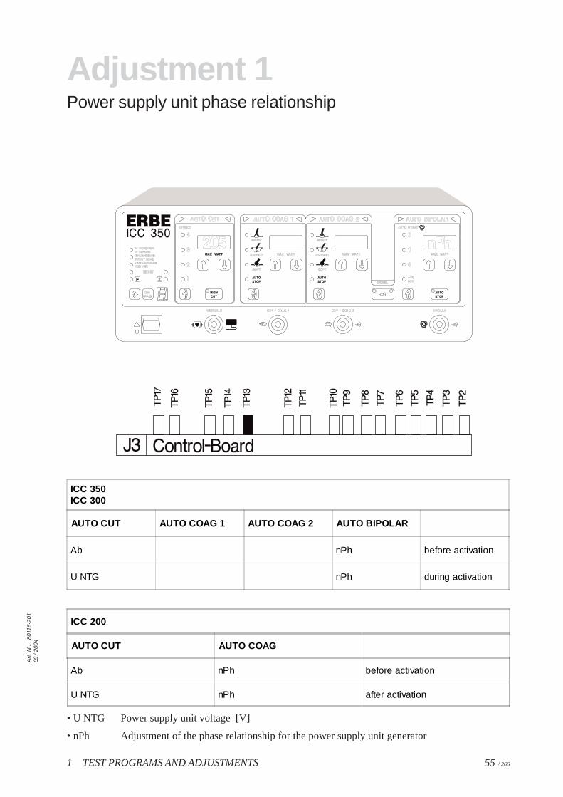
Adjustment 1

1 TEST PROGRAMS AND ADJUSTMENTS54 / 266
Adjustment 1Power supply unit phase relationship
Procedure
• Unplug power cable from the ERBOTOM ICC.
• Pull off the black lines on the bridge-connected rectifier BR 1 on the motherboard and connect anadjustable isolating transformer to BR 1 in its place, the output voltage of which is adjusted to 0 V.With well prebalanced boards, a transformer with a fixed voltage of approx. 155 V AC can also beused.
ATTENTION !
For units which are set to 120 V, you must absolutely make certain that the Erbotom ICC is operated via anisolated transformer. In addition, the connection between J15 and J20 on the motherboard must be removedfrom J15.
• Connect 200 ohms load resistance (e.g. APM 600) to MP1 = GND and MP2 on the power module(slot J5).
• Connect the oscilloscope to MP1 = GND and MP2 = probe on QC power stage end stage (slot J4).
• Plug the power cable for the Erbotom ICC back in and activate Test program 16, Adjustment 1.
• Activate using the yellow pedal on the footswitch (AUTO CUT).
• Slowly increase the output voltage on the isolating transformer. With a correct setting, the voltagecharacteristic corresponds to the graph illustrated below, whereby the small dip (approx. 20 V) nextto the square-wave edges represent a good criterion of evaluation for this.
• Set the phase angle using TP13 (control board, slot J3). For the final setting, the square-wave voltagemust be increased to approx. ±100 V. (Display in AUTO CUT approx. 205).
• After the setting is complete, disconnect the ERBOTOM ICC from the power, remove the cable fromthe isolating transformer to BR1 and connect the two black lines again to the bridge-connectedrectifier.
Fig.: Voltage characteristic of supply unit power
T
1 >
1) Ch 1: 50 Volt 500 ns
1 TEST PROGRAMS AND ADJUSTMENTS 55 / 266
Art
. No.
: 801
16-2
0109
/ 20
04
• U NTG Power supply unit voltage [V]
• nPh Adjustment of the phase relationship for the power supply unit generator
Adjustment 1Power supply unit phase relationship
ICC 350ICC 300
AUTO CUT AUTO COAG 1 AUTO COAG 2 AUTO BIPOLAR
Ab nPh before activation
U NTG nPh during activation
ICC 200
AUTO CUT AUTO COAG
Ab nPh before activation
U NTG nPh after activation

1 TEST PROGRAMS AND ADJUSTMENTS56 / 266

1 TEST PROGRAMS AND ADJUSTMENTS 57 / 266
Art
. No.
: 801
16-2
0109
/ 20
04
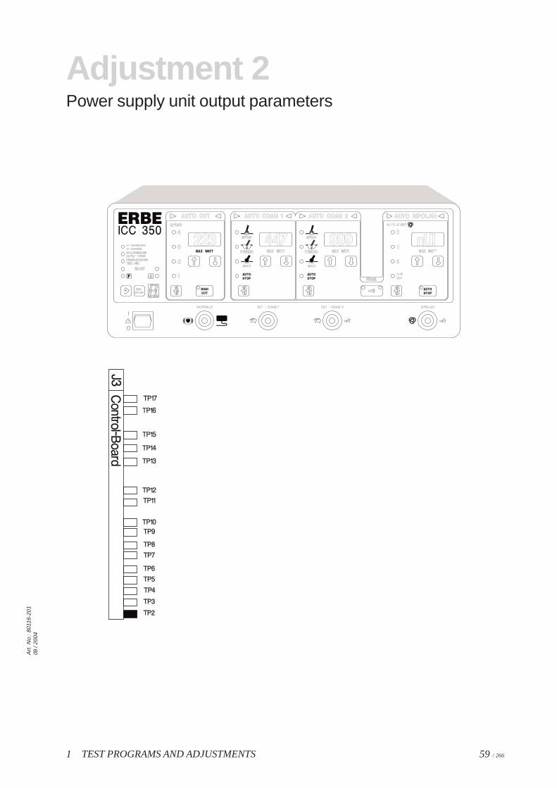
Adjustment 2

1 TEST PROGRAMS AND ADJUSTMENTS58 / 266
Adjustment 2Power supply unit output parameters
Procedure
• Connect 500 ohms load resistance (APM 600) to MP1 = GND and MP2 = +U on “Power Module”board (slot J5).
• Plug in the power cable on the ICC.
• Call up Test program 16, Adjustment 2.
• Activate ERBOTOM ICC using the yellow footswitch pedal (AUTO CUT).
• Set TP2 on the control board (slot J3) in such a way that 100 W (tolerance +0% / –7%) can bemeasured at the HF power meter and a power supply current of 447 mA (tolerance 444...455 mA) isdisplayed in the AUTO COAG 1 display. In the AUTO CUT display, a power supply voltage of 223V (tolerance 223…227 V) is displayed.
• Disconnect the ICC from the power and remove the connecting cable from MP1 and MP2.
ICC 350ICC 300
AUTO CUT AUTO COAG 1 AUTO COAG 2 AUTO BIPOLAR
Ab 2 nUI before activation
U NTG I NTG I NTG V1 nUI during activation
• U NTG Power supply voltage [V]; Set value = 223 V
• I NTG Power supply current [mA]; Set value = 447 mA
• I NTG V1 Amplified power supply current [mA]
• nUI Adjustment of the current voltage setting of the power supply generator
ICC 200
AUTO CUT AUTO COAG
nUI before activation
U NTG I NTG after activation
• U NTG Power supply voltage [V]; Set value = 223 V
• I NTG Power supply current [mA]; Set value = 447 mA
1 TEST PROGRAMS AND ADJUSTMENTS 59 / 266
Art
. No.
: 801
16-2
0109
/ 20
04
Adjustment 2Power supply unit output parameters

1 TEST PROGRAMS AND ADJUSTMENTS60 / 266

1 TEST PROGRAMS AND ADJUSTMENTS 61 / 266
Art
. No.
: 801
16-2
0109
/ 20
04
Adjustment 3

1 TEST PROGRAMS AND ADJUSTMENTS62 / 266
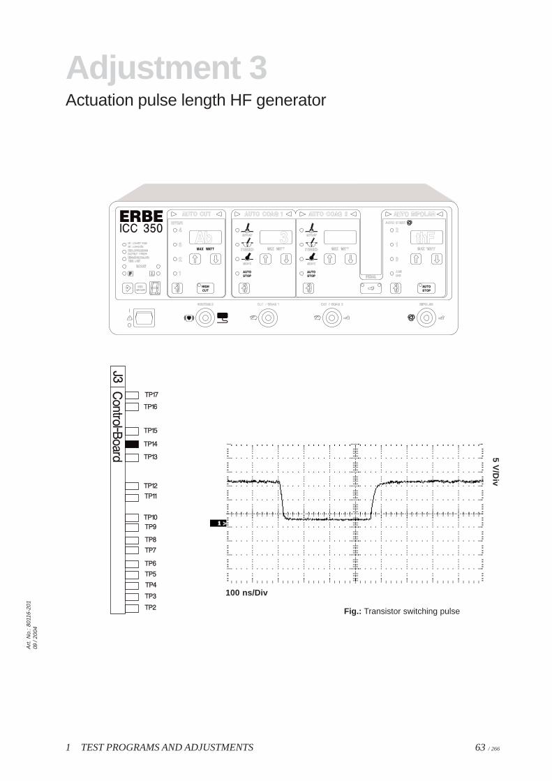
Adjustment 3Actuation pulse length HF generator
Procedure
• Measure the actuation pulse TS1 on the control board (slot J3) with an oscilloscope at measuringpoint MP6 = GND and MP2 = probe tip.
• Switch on the ICC and call up Test program 16, Adjustment 3.
• Using TP14 on the control board (slot J3), set a pulse length of 350 ns.
ATTENTION: Pulse is inverted.
• Disconnect the ICC from the power.
• Remove the probe from MP6 and MP2.
ICC 350ICC 300
AUTO CUT AUTO COAG 1 AUTO COAG 2 AUTO BIPOLAR
Ab 3 thF auto. activated
• thF Pulse length of the HF generator [ms]; Set value = 350 ns
ICC 200
AUTO CUT AUTO COAG
thF auto. activated
• thF Pulse length of the HF generator [ms]; Set value = 350 ns
1 TEST PROGRAMS AND ADJUSTMENTS 63 / 266
Art
. No.
: 801
16-2
0109
/ 20
04
Adjustment 3Actuation pulse length HF generator
Fig.: Transistor switching pulse
100 ns/Div
5 V/D
iv

1 TEST PROGRAMS AND ADJUSTMENTS64 / 266

1 TEST PROGRAMS AND ADJUSTMENTS 65 / 266
Art
. No.
: 801
16-2
0109
/ 20
04
Adjustment 4
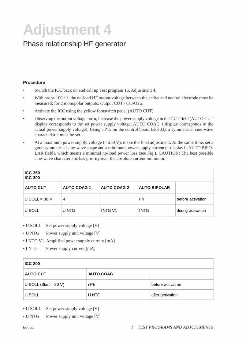
1 TEST PROGRAMS AND ADJUSTMENTS66 / 266
Procedure
• Switch the ICC back on and call up Test program 16, Adjustment 4.
• With probe 100 : 1, the no-load HF output voltage between the active and neutral electrode must bemeasured; for 2 monopolar outputs: Output CUT / COAG 2.
• Activate the ICC using the yellow footswitch pedal (AUTO CUT).
• Observing the output voltage form, increase the power supply voltage in the CUT field (AUTO CUTdisplay corresponds to the set power supply voltage; AUTO COAG 1 display corresponds to theactual power supply voltage). Using TP15 on the control board (slot J3), a symmetrical sine-wavecharacteristic must be set.
• At a maximum power supply voltage (= 250 V), make the final adjustment. At the same time, set agood symmetrical sine-wave shape and a minimum power supply current (= display in AUTO BIPO-LAR field), which means a minimal no-load power loss (see Fig.). CAUTION: The best possiblesine-wave characteristic has priority over the absolute current minimum.
ICC 350ICC 300
AUTO CUT AUTO COAG 1 AUTO COAG 2 AUTO BIPOLAR
U SOLL = 30 V 4 Ph before activation
U SOLL U NTG I NTG V1 I NTG during activation
• U SOLL Set power supply voltage [V]
• U NTG Power supply unit voltage [V]
• I NTG V1 Amplified power supply current [mA]
• I NTG Power supply current [mA]
ICC 200
AUTO CUT AUTO COAG
U SOLL (Start = 30 V) nPh before activation
U SOLL U NTG after activation
• U SOLL Set power supply voltage [V]
• U NTG Power supply unit voltage [V]
Adjustment 4Phase relationship HF generator

1 TEST PROGRAMS AND ADJUSTMENTS 67 / 266
Art
. No.
: 801
16-2
0109
/ 20
04
Adjustment 4Phase relationship HF generator
Fig.: HF no-load voltage
500 ns/Div
300 V/D
iv

1 TEST PROGRAMS AND ADJUSTMENTS68 / 266

1 TEST PROGRAMS AND ADJUSTMENTS 69 / 266
Art
. No.
: 801
16-2
0109
/ 20
04
Adjustment 5
1 TEST PROGRAMS AND ADJUSTMENTS70 / 266
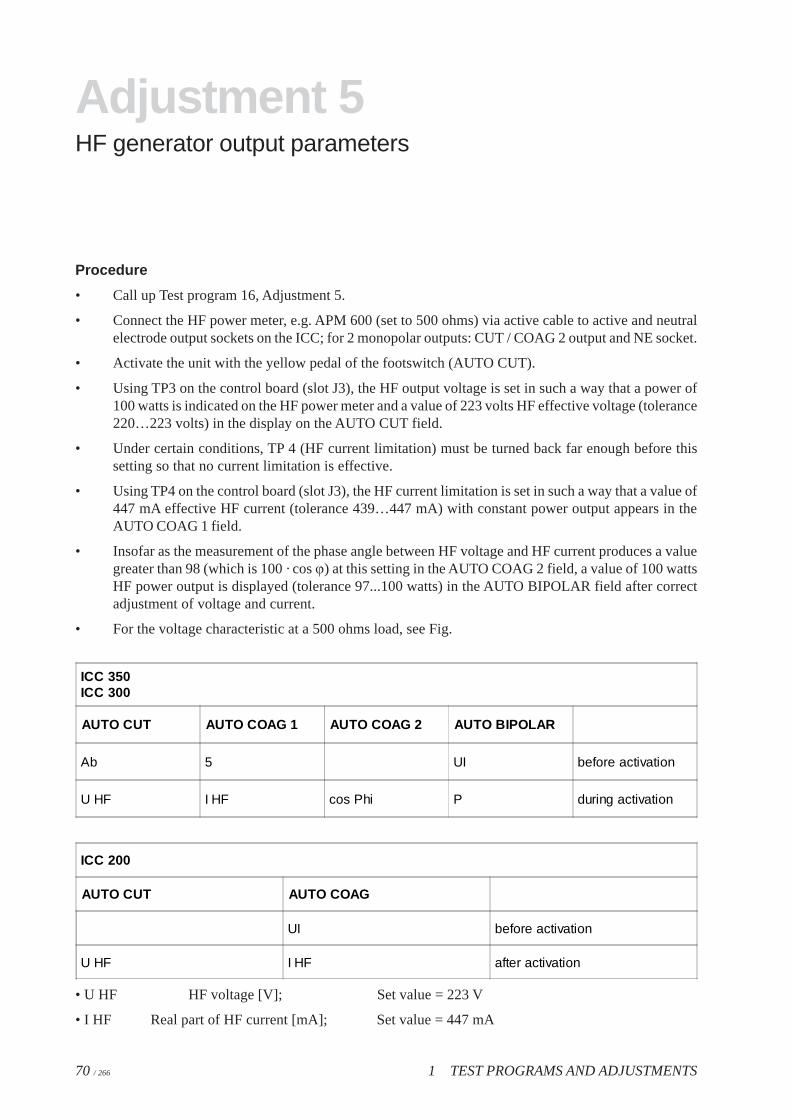
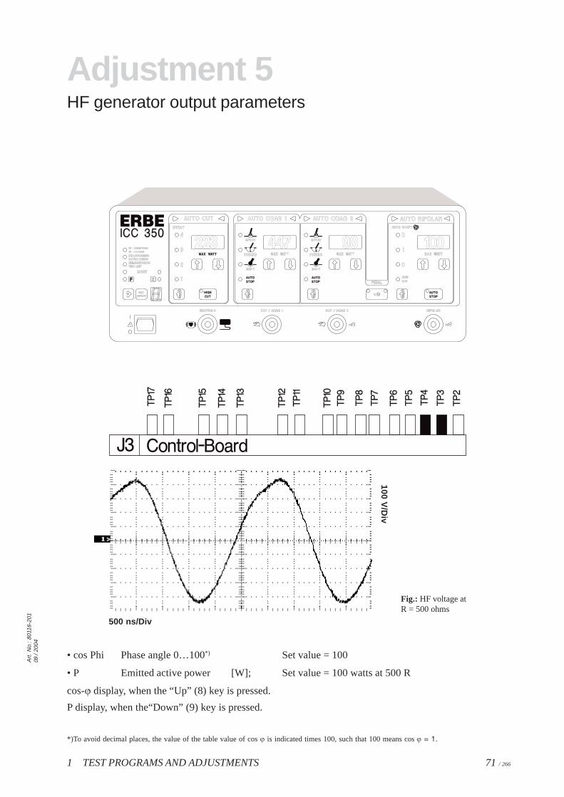
Adjustment 5HF generator output parameters
Procedure
• Call up Test program 16, Adjustment 5.
• Connect the HF power meter, e.g. APM 600 (set to 500 ohms) via active cable to active and neutralelectrode output sockets on the ICC; for 2 monopolar outputs: CUT / COAG 2 output and NE socket.
• Activate the unit with the yellow pedal of the footswitch (AUTO CUT).
• Using TP3 on the control board (slot J3), the HF output voltage is set in such a way that a power of100 watts is indicated on the HF power meter and a value of 223 volts HF effective voltage (tolerance220…223 volts) in the display on the AUTO CUT field.
• Under certain conditions, TP 4 (HF current limitation) must be turned back far enough before thissetting so that no current limitation is effective.
• Using TP4 on the control board (slot J3), the HF current limitation is set in such a way that a value of447 mA effective HF current (tolerance 439…447 mA) with constant power output appears in theAUTO COAG 1 field.
• Insofar as the measurement of the phase angle between HF voltage and HF current produces a valuegreater than 98 (which is 100 · cos j) at this setting in the AUTO COAG 2 field, a value of 100 wattsHF power output is displayed (tolerance 97...100 watts) in the AUTO BIPOLAR field after correctadjustment of voltage and current.
• For the voltage characteristic at a 500 ohms load, see Fig.
ICC 350ICC 300
AUTO CUT AUTO COAG 1 AUTO COAG 2 AUTO BIPOLAR
Ab 5 UI before activation
U HF I HF cos Phi P during activation
ICC 200
AUTO CUT AUTO COAG
UI before activation
U HF I HF after activation
• U HF HF voltage [V]; Set value = 223 V
• I HF Real part of HF current [mA]; Set value = 447 mA
1 TEST PROGRAMS AND ADJUSTMENTS 71 / 266
Art
. No.
: 801
16-2
0109
/ 20
04
• cos Phi Phase angle 0…100*) Set value = 100
• P Emitted active power [W]; Set value = 100 watts at 500 R
cos-j display, when the “Up” (8) key is pressed.
P display, when the“Down” (9) key is pressed.
*)To avoid decimal places, the value of the table value of cos j is indicated times 100, such that 100 means cos j = 1.
Adjustment 5HF generator output parameters
Fig.: HF voltage atR = 500 ohms
500 ns/Div
100 V/D
iv

1 TEST PROGRAMS AND ADJUSTMENTS72 / 266

1 TEST PROGRAMS AND ADJUSTMENTS 73 / 266
Art
. No.
: 801
16-2
0109
/ 20
04
Adjustment 6
1 TEST PROGRAMS AND ADJUSTMENTS74 / 266
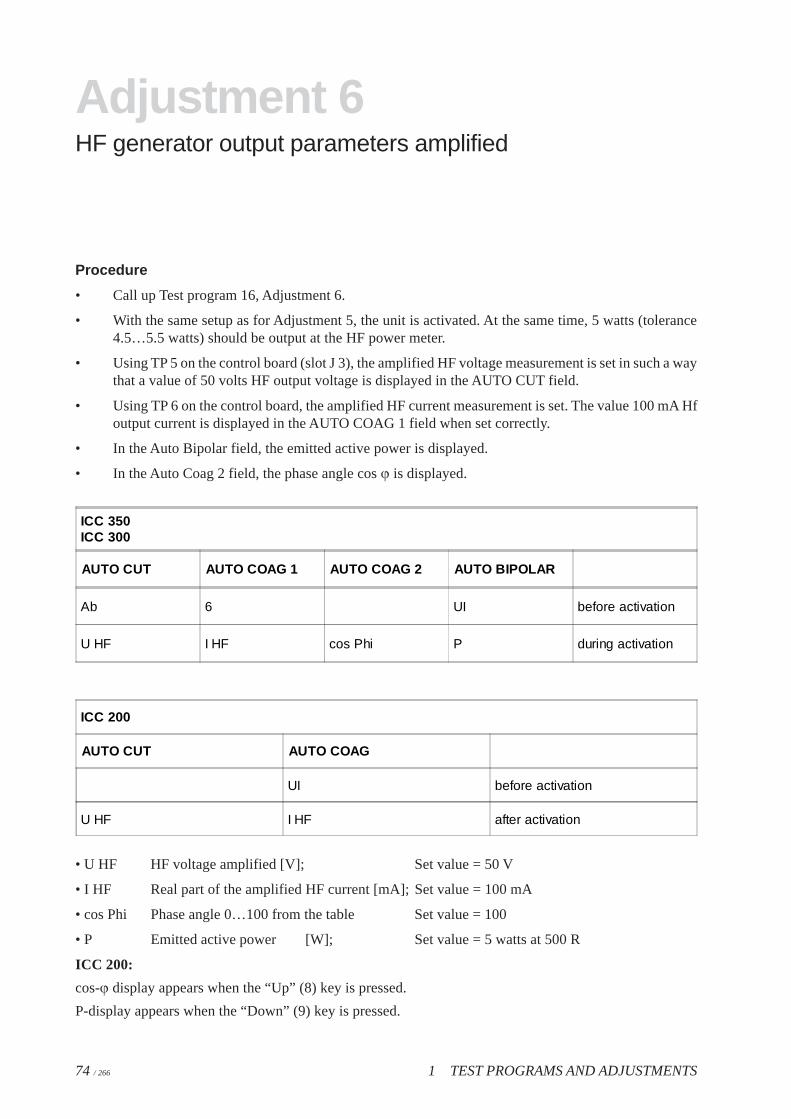
Procedure
• Call up Test program 16, Adjustment 6.
• With the same setup as for Adjustment 5, the unit is activated. At the same time, 5 watts (tolerance4.5…5.5 watts) should be output at the HF power meter.
• Using TP 5 on the control board (slot J 3), the amplified HF voltage measurement is set in such a waythat a value of 50 volts HF output voltage is displayed in the AUTO CUT field.
• Using TP 6 on the control board, the amplified HF current measurement is set. The value 100 mA Hfoutput current is displayed in the AUTO COAG 1 field when set correctly.
• In the Auto Bipolar field, the emitted active power is displayed.
• In the Auto Coag 2 field, the phase angle cos j is displayed.
ICC 350ICC 300
AUTO CUT AUTO COAG 1 AUTO COAG 2 AUTO BIPOLAR
Ab 6 UI before activation
U HF I HF cos Phi P during activation
ICC 200
AUTO CUT AUTO COAG
UI before activation
U HF I HF after activation
• U HF HF voltage amplified [V]; Set value = 50 V
• I HF Real part of the amplified HF current [mA]; Set value = 100 mA
• cos Phi Phase angle 0…100 from the table Set value = 100
• P Emitted active power [W]; Set value = 5 watts at 500 R
ICC 200:
cos-j display appears when the “Up” (8) key is pressed.
P-display appears when the “Down” (9) key is pressed.
Adjustment 6HF generator output parameters amplified
1 TEST PROGRAMS AND ADJUSTMENTS 75 / 266
Art
. No.
: 801
16-2
0109
/ 20
04
Adjustment 6HF generator output parameters amplified

1 TEST PROGRAMS AND ADJUSTMENTS76 / 266

1 TEST PROGRAMS AND ADJUSTMENTS 77 / 266
Art
. No.
: 801
16-2
0109
/ 20
04
Adjustment 7

1 TEST PROGRAMS AND ADJUSTMENTS78 / 266
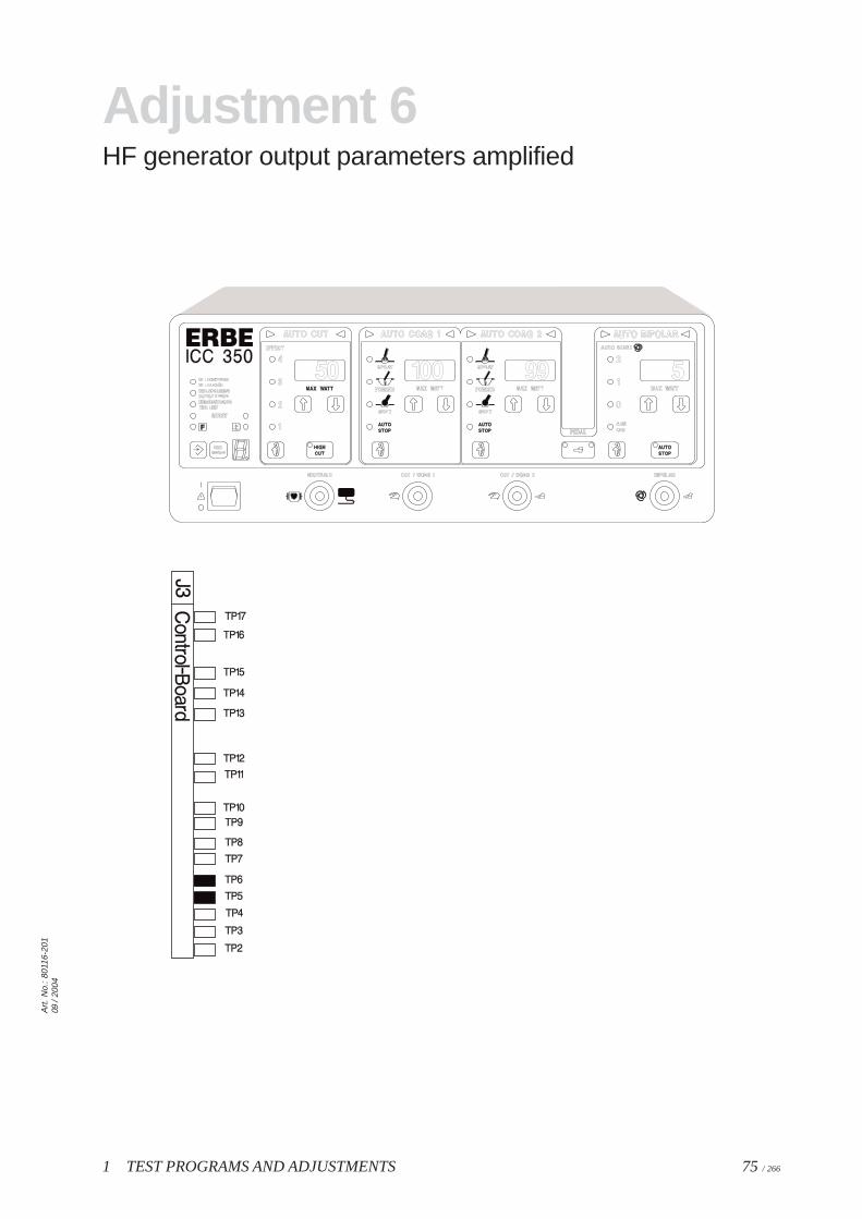
Adjustment 7Phase angle (cos j)
Procedure
• Call up Test program 16, Adjustment 7.
• Using ERBE original cable, connect the APM 600 (set at 500 ohms) to the ICC; with 2 monopolarconnections: Connect active output socket: CUT / COAG 2 (ICC 300 / 350) and NE socket.
• Connect a capacitor with 1 nF (e.g. ERBE component no. EE 51103-026) with short lines across theactive electrode and NE sockets on the HF power meter.
This produces a phase shift between voltage and current of 45° at a frequency of 340 kHz.
• Activate the cut footswitch.
• Using TP 7 on the control board (slot J3), the unit is set in such a way a value of 73 (display is100 · cos j) is displayed in the AUTO CUT field and a value of 120 (analog / digital convertermeasured value) is displayed in the AUTO COAG 1 field.
ICC 350ICC 300
AUTO CUT AUTO COAG 1 AUTO COAG 2 AUTO BIPOLAR
Ab 7 PHI before activation
COS xxx PHI during activation
ICC 200
AUTO CUT AUTO COAG
PHI before activation
COS xxx after activation
• COS cos-j values from table; Set value = 73
0 means phase shifting = 90°
100 means phase shifting = 0°
• xxx Analog cos-j measurement value; Range 0…255
• Veff
HF output voltage;
200 mA output current limitation
1 TEST PROGRAMS AND ADJUSTMENTS 79 / 266
Art
. No.
: 801
16-2
0109
/ 20
04
Adjustment 7Phase angle (cos j)

1 TEST PROGRAMS AND ADJUSTMENTS80 / 266

1 TEST PROGRAMS AND ADJUSTMENTS 81 / 266
Art
. No.
: 801
16-2
0109
/ 20
04
Adjustment 8

1 TEST PROGRAMS AND ADJUSTMENTS82 / 266
Adjustment 8Spark monitor
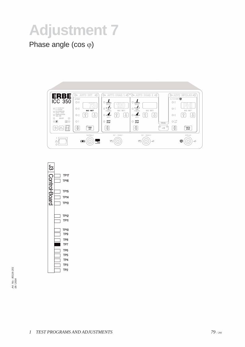
Procedure (also applies to the units without HIGH CUT or ENDO CUT)
• On the ICC 300 and ICC 200 without ENDOCUT, TP8 should be set to the upper limit (to do this,turn TP8 clockwise).
• Call up Test program 16, Adjustment 8.
• A DC voltage of 70 volts is fed into the patient circuit between the center control for the active AEsocket (with 2 monopolar outputs: Output CUT / COAG 2) and the neutral electrode NE socket (AE =+, NE = –). To do this, the ERBE TESTBOX 70 volts is recommended (ERBE Order no. 20100-019).
• Adjust TP8 on the control board (slot J3) is set in such a way that a measurement value of 77 isindicated for the A/D converter, and a value of 70 volts DC is displayed in the AUTO COAG 1 field.On the ICC 200 ENDOCUT, this value appears in the AUTO CUT field, while the A/D convertervalue is not shown.
ICC 350
AUTO CUT AUTO COAG 1 AUTO COAG 2 AUTO BIPOLAR
xxx yyy FU Standby
ICC 200 ENDO CUT
AUTO CUT AUTO COAG
yyy FU Standby
• yyy Fed-in DC voltage for the spark measurement value (70 V)
• xxx Analog spark measurement value
The input for applying the test DC voltage is the CUT / COAG 2 socket.
1 TEST PROGRAMS AND ADJUSTMENTS 83 / 266
Art
. No.
: 801
16-2
0109
/ 20
04
Adjustment 8Spark monitor

1 TEST PROGRAMS AND ADJUSTMENTS84 / 266

1 TEST PROGRAMS AND ADJUSTMENTS 85 / 266
Art
. No.
: 801
16-2
0109
/ 20
04
Adjustment 9
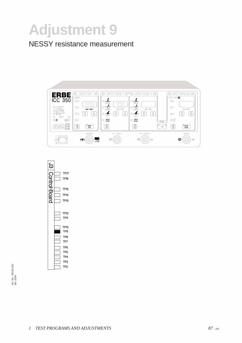
1 TEST PROGRAMS AND ADJUSTMENTS86 / 266
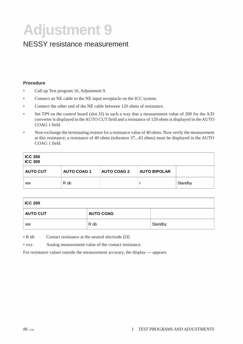
Adjustment 9NESSY resistance measurement
Procedure
• Call up Test program 16, Adjustment 9.
• Connect an NE cable to the NE input receptacle on the ICC system.
• Connect the other end of the NE cable between 120 ohms of resistance.
• Set TP9 on the control board (slot J3) in such a way that a measurement value of 200 for the A/Dconverter is displayed in the AUTO CUT field and a resistance of 120 ohms is displayed in the AUTOCOAG 1 field.
• Now exchange the terminating resistor for a resistance value of 40 ohms. Now verify the measurementat this resistance; a resistance of 40 ohms (tolerance 37...43 ohms) must be displayed in the AUTOCOAG 1 field.
ICC 350ICC 300
AUTO CUT AUTO COAG 1 AUTO COAG 2 AUTO BIPOLAR
xxx R üb r Standby
ICC 200
AUTO CUT AUTO COAG
xxx R üb Standby
• R üb Contact resistance at the neutral electrode [W]
• xxx Analog measurement value of the contact resistance.
For resistance values outside the measurement accurary, the display --- appears.
1 TEST PROGRAMS AND ADJUSTMENTS 87 / 266
Art
. No.
: 801
16-2
0109
/ 20
04
Adjustment 9NESSY resistance measurement

1 TEST PROGRAMS AND ADJUSTMENTS88 / 266

1 TEST PROGRAMS AND ADJUSTMENTS 89 / 266
Art
. No.
: 801
16-2
0109
/ 20
04
Adjustment 10

1 TEST PROGRAMS AND ADJUSTMENTS90 / 266
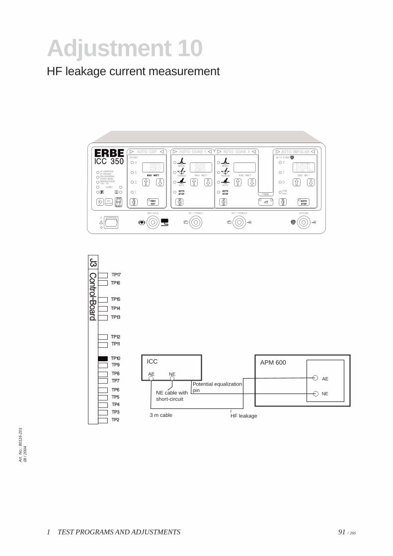
Adjustment 10HF leakage current measurement
Procedure (This adjustment only applies to the ICC 350)
• Call up Test program 16, Adjustment 10.
• Connect the HF power meter (set to 350 ohms load resistance) between the active electrode of theCUT / COAG 2 (center) socket and the potential equalization.
• Jumper J3 must be plugged into the display board for this adjustment (earthed reference).
• Short together the NE-ERBE original adapter cable. Activate the ICC 350 using the blue footswitchpedal (AUTO COAG 1).
• Using the power setting in the AUTO COAG 1 field, set the leakage current flowing to ground to avalue of 150 mA
eff (tolerance 131…169 mA) (use an HF effective current meter or set a power of 7.9
watts at a HF power meter with a load resistance of 350 ohms [tolerance 6.0…10 watts (from P = I² · Rwith P = 7.9 watts and R = 350 ohms is a current I = 150 mA)]).
• Set TP10 on the control board (slot J3) in such a way that the HF leakage alarm is thus displayedvisually (the LED in the safety field flashes in the display indicates the value 50 in the Auto Cutfield).
• Increase the leakage current by changing the power setting until an audible alarm is also emitted.This should occur at 300…350 mA (accordingly 31.5…43 watts on a HF power meter at the abovesetting).
ICC 350
AUTO CUT AUTO COAG 1 AUTO COAG 2 AUTO BIPOLAR
xxx ppp HFL Standby
• ppp Set SOFT COAG power which can be changed during activation.
• xxx Measurement value of the HF leakage current measurement.
Using the power setting in the AUTO COAG 1 field, set the HF leakage current flowing to ground atI
eff = 150 mA. This is not assigned for the ICC 200 and 300 since no HF leakage current monitor is
available there.
1 TEST PROGRAMS AND ADJUSTMENTS 91 / 266
Art
. No.
: 801
16-2
0109
/ 20
04
Adjustment 10HF leakage current measurement
AE NE
APM 600ICC
Potential equalizationpin
NE
AE
NE cable withshort-circuit
3 m cableIHF leakage

1 TEST PROGRAMS AND ADJUSTMENTS92 / 266

1 TEST PROGRAMS AND ADJUSTMENTS 93 / 266
Art
. No.
: 801
16-2
0109
/ 20
04
Adjustment 11

1 TEST PROGRAMS AND ADJUSTMENTS94 / 266
Adjustment 11Contact monitor
Procedure
• Call up Test program 16, Adjustment 11.
• At the BIPOLAR output of the ICC, the ERBE bipolar Testbox for the bipolar automatic starter (EE20100-017 ) or appropriate fixed resistors (1.2 kOhm and 2.5 kOhm with a capacity of 15 watts aswell as 18 kOhm, 1 watt) is connected via the EE bipolar original cable.
• With a resistance of 2.5 kOhm (socket 1–2), a value of 25 must be displayed in the AUTO CUT field.(Display = resistance divided by 100). The setting of the switch-on threshold with PT11 on the PCBcontrol board (slot J3) proceeds in such a way that, at a load resistance of 2.5 kOhm, the display inthe AUTO COAG 2 field changes from “OFF” to “ON”.
• Now the short-circuiting monitor is set by connecting a 6 ohm resistor (capacity = 0.5 watts) to theBIPOLAR outlet. Then, the display »rLo« appears on the AUTO COAG 1 display. Using TP12 on thePCB control board J3, the display is set to a measurement value of 100 in the AUTO CUT display.
• Testing the shutdown response: To do this, exit Test program 16 briefly by selecting Test program 0.The ICC operates in the normal mode. Switch on AUTO START 1. Set the bipolar power to 1 watt.The BIPOLAR outlet is connected to sockets 1 and 3 on the ERBE Testbox and thereby charged with1.2 kOhm. The BIPOLAR generator must automatically be activated after the delay time. Now presspushbutton 1 on the Testbox. This raises the capacity resistance to 18 kOhm. The BIPOLAR generatormust now shut down.
• This test must be repeated at the power settings 20 watts, 40 watts, 50 watts (or without AAMIstandard up to 120 watts).
ICC 350ICC 300
AUTO CUT AUTO COAG 1 AUTO COAG 2 AUTO BIPOLAR
uuu OFF br open output
rda ON br loaded output
iii rLo br loaded output
ICC 200
AUTO CUT AUTO COAG
uuu OFF open output
rda ON loaded output
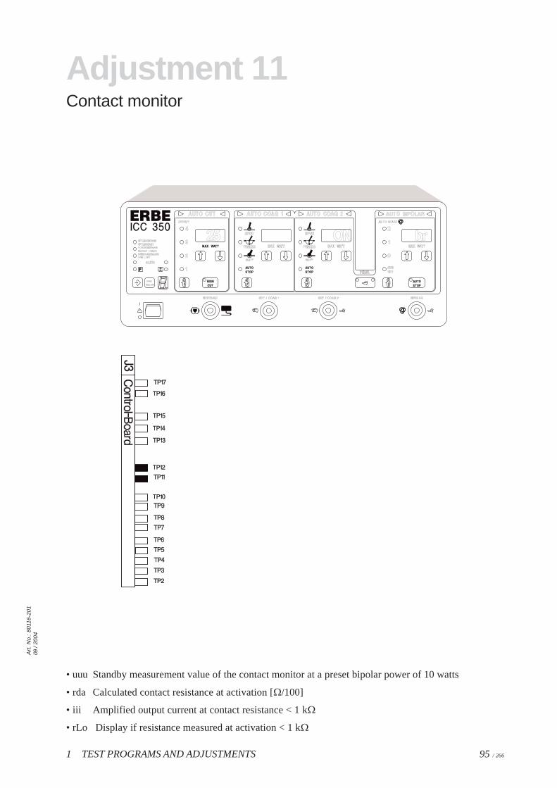
1 TEST PROGRAMS AND ADJUSTMENTS 95 / 266
Art
. No.
: 801
16-2
0109
/ 20
04
• uuu Standby measurement value of the contact monitor at a preset bipolar power of 10 watts
• rda Calculated contact resistance at activation [W/100]
• iii Amplified output current at contact resistance < 1 kW
• rLo Display if resistance measured at activation < 1 kW
Adjustment 11Contact monitor

1 TEST PROGRAMS AND ADJUSTMENTS96 / 266

1 TEST PROGRAMS AND ADJUSTMENTS 97 / 266
Art
. No.
: 801
16-2
0109
/ 20
04
Adjustment 12

1 TEST PROGRAMS AND ADJUSTMENTS98 / 266
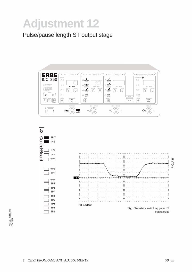
Adjustment 12Pulse/pause length ST output stage
Procedure
• Call up Test program 16, Adjustment 12.
• Measure actuation impulse TSI_STE at measuring point MP 3 on ST output stage (slot J6) with theoscilloscope (measuring point MP1 = GND).
• Using TP16, set this to a pulse length of 200 ns (±50 ns).
IMPORTANT! The pulse time is measured at average amplitude, i.e. at approx. 7.5 volts level.
ATTENTION! The pulse is inverted.
• The repetition frequency at TP17 is set in such a way that the value 0 (tolerance 0...4) is displayed inthe AUTO CUT field.
• Now exit the test program and return the ICC to normal operating condition.
• To check the performance, connect the HF output to the HF power meter, setting 500 ohms.
• Activate the ICC using the blue footswitch pedal at the SPRAY and FORCED normal settings. Thepower output in watts should correspond to the display in the AUTO COAG 2 field.
• Check whether the maximum emitted output power with SPRAY and FORCED is within the tolerancelimits (120 W ± 15 %). If necessary, conform the pulse length to the PCB control board using TP16.TP17 must no longer be changed.
ICC 350ICC 300
AUTO CUT AUTO COAG 1 AUTO COAG 2 AUTO BIPOLAR
xxx ppp tSt Standby
ICC 200
AUTO CUT AUTO COAG
xxx tSt Standby
• ppp Set AUTO COAG 2 FORCED power
• xxx Difference = Set frequency minus actual frequency
1 TEST PROGRAMS AND ADJUSTMENTS 99 / 266
Art
. No.
: 801
16-2
0109
/ 20
04
Adjustment 12Pulse/pause length ST output stage
Fig. : Transistor switching pulse SToutput stage
50 ns/Div
5 V/D
iv

1 TEST PROGRAMS AND ADJUSTMENTS100 / 266

1 TEST PROGRAMS AND ADJUSTMENTS 101 / 266
Art
. No.
: 801
16-2
0109
/ 20
04
Adjustment 13

1 TEST PROGRAMS AND ADJUSTMENTS102 / 266
Adjustment 13LF leakage current monitor (ICC 350 only)
Procedure
• Call up Test program 16, Adjustment 13.
• Set the jumper to the “capacitance grounded” operating mode (place jumper J3 on display board).
• Perform adjustment using ERBE TESTBOX 2 or another 50 Hz sine-wave current source.
• Between the neutral electrode output and the potential equalization, feed a 50 Hz sine-wave currentof 45 µA (see Figure).
• Using TP1 on the motherboard, set the leakage current monitor in such a way that the display in theAUTO CUT field changes just from 0 to 1 at 45 µA
eff.
Reset jumper to previous condition.
ICC 350
AUTO CUT AUTO COAG 1 AUTO COAG 2 AUTO BIPOLAR
x I nF Standby
• x x = 0 for LF leakage current < 50 µA
x = 1 for LF leakage current > 50 µA.
For adjustment, the test current must be fed according to the instructions.
Adjustment 13 is not assigned on the ICC 300 and ICC 200.
Measurement setup
AE NE
ERBETestbox 2 18
19
INF
ICC
Battery-poweredmeasurement unitonly!
PE
LI
N
Powersupply
110 V115 V230 V
+
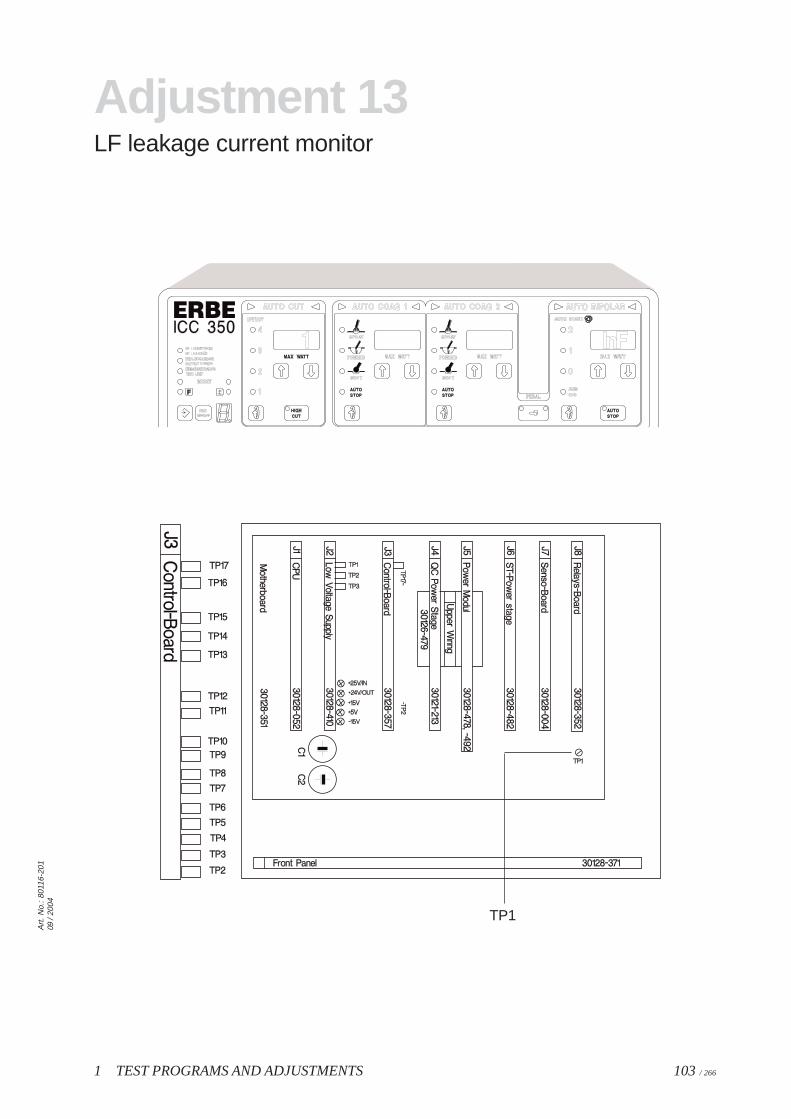
1 TEST PROGRAMS AND ADJUSTMENTS 103 / 266
Art
. No.
: 801
16-2
0109
/ 20
04
Adjustment 13LF leakage current monitor
TP1

1 TEST PROGRAMS AND ADJUSTMENTS104 / 266
1 TEST PROGRAMS AND ADJUSTMENTS 105 / 266
Art
. No.
: 801
16-2
0109
/ 20
04
Adjustment ofICC 350 ZMK Neurotest
Version V2.00ICC 350 TUR Neurotest
Version V2.00

1 TEST PROGRAMS AND ADJUSTMENTS106 / 266
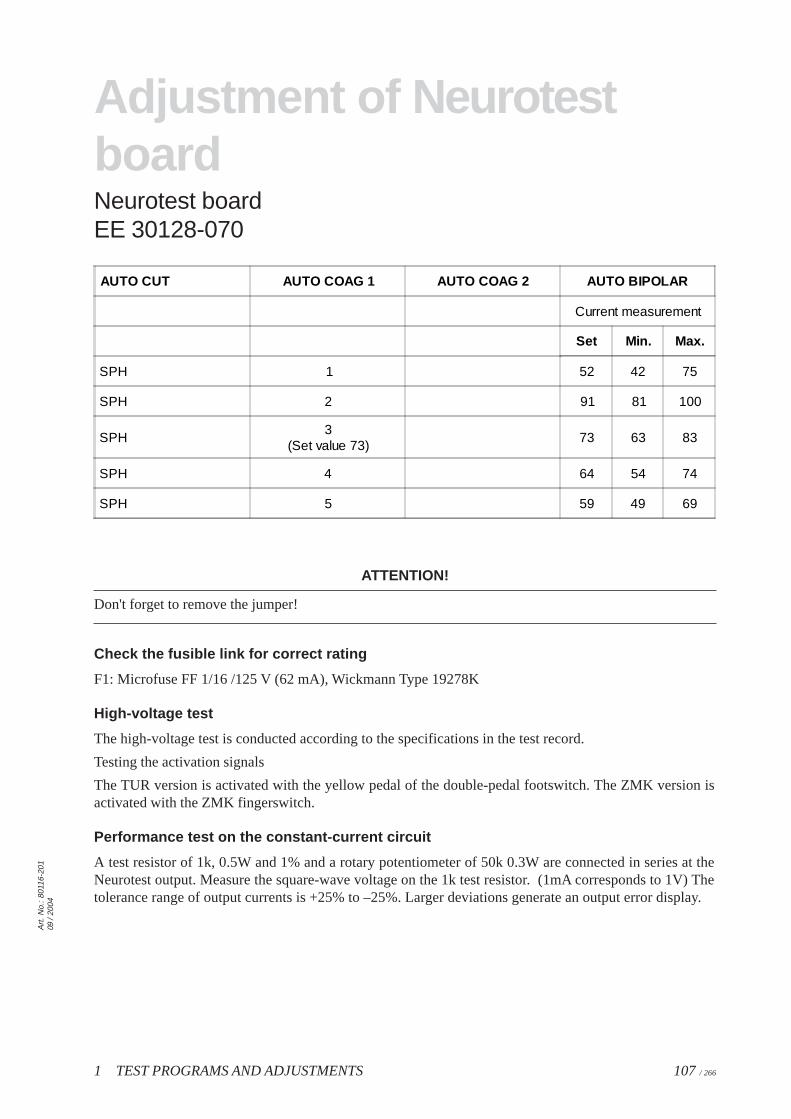
Adjustment of NeurotestboardNeurotest boardEE 30128-070
Jumper JP4 on the front panel is used to activate the display of the feedback frequency of output currentmeasurement and display of the feedback frequency of the remote control are activated.
ATTENTION
On the ZMK version, there is a display only during activation and if the Neurotest circuit is closed. On theTUR version there is a display as soon as the NT LED lights up on the remote control.
AUTO CUT AUTO COAG 1 AUTO COAG 2 AUTO BIPOLAR
SPH Intensity no. Frequency measurement Current measurement
SPH: The Neurotest program is activated.
Intensity no. Set intensity number is 1…5. It corresponds to the intensity number which has been seton the remote control.
Frequency measurement Measurement of feedback frequency of the remote control.
Current measurement Measurement of feedback frequency of the output current measurement.
Setting the feedback frequency of output current measurement
(trimming potentiometer TP 1: Setting the feedback frequency)
The Neurotest board is isolated and actuated via optocoupler. The feedback frequency of the output currentmeasurement also takes place via an optocoupler. The output current pulse is converted into a frequency.This frequency can be measured at test point MP7. Test point MP6 is reference ground. Test points MP6 andMP7 relate to the electronic circuitry of the ICC unit. Without activation, the feedback frequency is 0 Hz.After the pulse time, the feedback frequency is only available at MP7 for a brief period.
Test setup
At the Neurotest output, connect up a test resistor of 1 kOhm, 0.5 W and 1%. On the TUR version, theNeurotest output is between the neutral electrode and the CUT/COAG 2 output. The TUR version is activatedwith the yellow pedal of the dual-pedal footswitch. On the ZMK version the Neurotest output is between theneutral electrode and the Neurotest output. The ZMK version is activated with the ZMK fingerswitch.
The setting is performed at intensity 3. For this setting the set feedback frequency must be adjusted to 73. Ifthe electronic fuse trips, the display of feedback frequency is approx. 40.
1 TEST PROGRAMS AND ADJUSTMENTS 107 / 266
Art
. No.
: 801
16-2
0109
/ 20
04
Adjustment of NeurotestboardNeurotest boardEE 30128-070
AUTO CUT AUTO COAG 1 AUTO COAG 2 AUTO BIPOLAR
Current measurement
Set Min. Max.
SPH 1 52 42 75
SPH 2 91 81 100
SPH3
(Set value 73)73 63 83
SPH 4 64 54 74
SPH 5 59 49 69
ATTENTION!
Don't forget to remove the jumper!
Check the fusible link for correct rating
F1: Microfuse FF 1/16 /125 V (62 mA), Wickmann Type 19278K
High-voltage test
The high-voltage test is conducted according to the specifications in the test record.
Testing the activation signals
The TUR version is activated with the yellow pedal of the double-pedal footswitch. The ZMK version isactivated with the ZMK fingerswitch.
Performance test on the constant-current circuit
A test resistor of 1k, 0.5W and 1% and a rotary potentiometer of 50k 0.3W are connected in series at theNeurotest output. Measure the square-wave voltage on the 1k test resistor. (1mA corresponds to 1V) Thetolerance range of output currents is +25% to –25%. Larger deviations generate an output error display.

1 TEST PROGRAMS AND ADJUSTMENTS108 / 266
Adjustment of NeurotestboardNeurotest boardEE 30128-070
Square-wave output peak current Control range of constant-current source
SPH 1: 5 mA 0R…approx. 20 kOhm
SPH 2: 10 mA 0R…approx. 10 kOhm
SPH 3: 15 mA 0R…approx. 6 kOhm
SPH 4: 20 mA 0R…approx. 5 kOhm
SPH 5: 25 mA 0R…approx. 4 kOhm
Testing the constant-current source
Slowly set the rotary potentiometer higher from 0R. At a total resistance of approx. 6 kOhm, there is anoutput error display. At approx. 6 kOhm, the output current is constant.
Performance test on output error monitoring.
• At the Neurotest output connect a test resistor of 1 kOhm, 0.5 W and 1%.
• Set SPH 1.
• Activate the unit. When the circuit is interrupted there will be an output error message.
Performance test on the electronic fuse
The output current is monitored constantly. In the event of an excess dose, the electronic fuse trips and vialongitudinal transistor T3 switches off the constant-current source supply voltage. The electronic fuse ismonitored in the interval between the pulses. If the electronic fuse has tripped, this is indicated by themessage ERROR 90 or ERROR 84.
• To trip the electronic fuse: Activate the Neurotest function and briefly connect test point MP9 to MP2.The electronic fuse should respond. The microfuse must not trip.
General information about the self-check
Before activation, or when setting the intensity on the remote control, there is a check on the electronic fusein two steps.
1. Briefly switch on transistor T1 and thus trip the electronic fuse. There is a message ERROR 90 orERROR 84 if the electronic fuse has tripped.
2. Briefly switch on transistor T2 and thus reset the electronic fuse. There is a message if the electronicfuse has not been reset.

1 TEST PROGRAMS AND ADJUSTMENTS 109 / 266
Art
. No.
: 801
16-2
0109
/ 20
04
Adjustment of NeurotestboardNeurotest boardEE 30128-070
Activation test
Activation of the HF LED on the remote control takes place at intensity setting 0 using the rotary switch onPC board EE 30121-442. At an intensity setting of 1 to 5 the NT LED is actuated by the CPU and the HFLED must not light up. On the TUR version a check must be performed as to whether activation of the HFis inhibited when intensity of 1 ... 5 is set. On the ZMK version, activation of the HF is possible even ifintensity 1 ... 5 has been set.

1 TEST PROGRAMS AND ADJUSTMENTS110 / 266

1 TEST PROGRAMS AND ADJUSTMENTS 111 / 266
Art
. No.
: 801
16-2
0109
/ 20
04
Adjustment ofremote control for
Neurotest
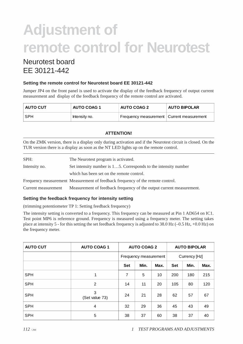
1 TEST PROGRAMS AND ADJUSTMENTS112 / 266
Adjustment ofremote control for NeurotestNeurotest boardEE 30121-442
Setting the remote control for Neurotest board EE 30121-442
Jumper JP4 on the front panel is used to activate the display of the feedback frequency of output currentmeasurement and display of the feedback frequency of the remote control are activated.
AUTO CUT AUTO COAG 1 AUTO COAG 2 AUTO BIPOLAR
SPH Intensity no. Frequency measurement Current measurement
ATTENTION!
On the ZMK version, there is a display only during activation and if the Neurotest circuit is closed. On theTUR version there is a display as soon as the NT LED lights up on the remote control.
SPH: The Neurotest program is activated.
Intensity no. Set intensity number is 1…5. Corresponds to the intensity number
which has been set on the remote control.
Frequency measurement Measurement of feedback frequency of the remote control.
Current measurement Measurement of feedback frequency of the output current measurement.
Setting the feedback frequency for intensity setting
(trimming potentiometer TP 1: Setting feedback frequency)
The intensity setting is converted to a frequency. This frequency can be measured at Pin 1 AD654 on IC1.Test point MP6 is reference ground. Frequency is measured using a frequency meter. The setting takesplace at intensity 5 - for this setting the set feedback frequency is adjusted to 38.0 Hz (–0.5 Hz, +0.0 Hz) onthe frequency meter.
AUTO CUT AUTO COAG 1 AUTO COAG 2 AUTO BIPOLAR
Frequency measurement Currency [Hz]
Set Min. Max. Set Min. Max.
SPH 1 7 5 10 200 180 215
SPH 2 14 11 20 105 80 120
SPH3
(Set value 73)24 21 28 62 57 67
SPH 4 32 29 36 45 43 49
SPH 5 38 37 60 38 37 40

1 TEST PROGRAMS AND ADJUSTMENTS 113 / 266
Art
. No.
: 801
16-2
0109
/ 20
04
Adjustment ofremote control for NeurotestNeurotest boardEE 30121-442
ATTENTION!
Don’t forget to remove the jumper.
Setting the feedback frequency for intensity adjustment can also be performed without the ICC unit bysupplying +15 V to the remote control and measuring the feedback frequency using the frequency meter.
High-voltage test
The high-voltage test is performed using the specifications in the test record.
Testing the LED display
Actuation of the HF LED is conducted at intensity setting 0 using the rotary switch PC board on EE 30121-442. At an intensity setting of 1 to 5, the NT LED is actuated by the CPU and the HF LED must not light up.The NT LED only lights up when the feedback frequency is in the valid range. Check intensity setting 1…5.

1 TEST PROGRAMS AND ADJUSTMENTS114 / 266
1 TEST PROGRAMS AND ADJUSTMENTS 115 / 266
Art
. No.
: 801
16-2
0109
/ 20
04
Adjustment ofactivation
and instrument detection
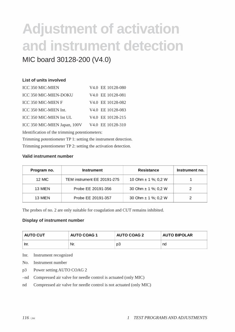
1 TEST PROGRAMS AND ADJUSTMENTS116 / 266
Adjustment of activationand instrument detectionMIC board 30128-200 (V4.0)
List of units involved
ICC 350 MIC-MIEN V4.0 EE 10128-080
ICC 350 MIC-MIEN-DOKU V4.0 EE 10128-081
ICC 350 MIC-MIEN F V4.0 EE 10128-082
ICC 350 MIC-MIEN Int. V4.0 EE 10128-083
ICC 350 MIC-MIEN Int UL V4.0 EE 10128-215
ICC 350 MIC-MIEN Japan, 100V V4.0 EE 10128-310
Identification of the trimming potentiometers:
Trimming potentiometer TP 1: setting the instrument detection.
Trimming potentiometer TP 2: setting the activation detection.
Valid instrument number
Program no. Instrument Resistance Instrument no.
12 MIC TEM instrument EE 20191-275 10 Ohm ± 1 %; 0,2 W 1
13 MIEN Probe EE 20191-356 30 Ohm ± 1 %; 0,2 W 2
13 MIEN Probe EE 20191-357 30 Ohm ± 1 %; 0,2 W 2
The probes of no. 2 are only suitable for coagulation and CUT remains inhibited.
Display of instrument number
AUTO CUT AUTO COAG 1 AUTO COAG 2 AUTO BIPOLAR
Inr. Nr. p3 nd
Inr. Instrument recognized
No. Instrument number
p3 Power setting AUTO COAG 2
–nd Compressed air valve for needle control is actuated (only MIC)
nd Compressed air valve for needle control is not actuated (only MIC)
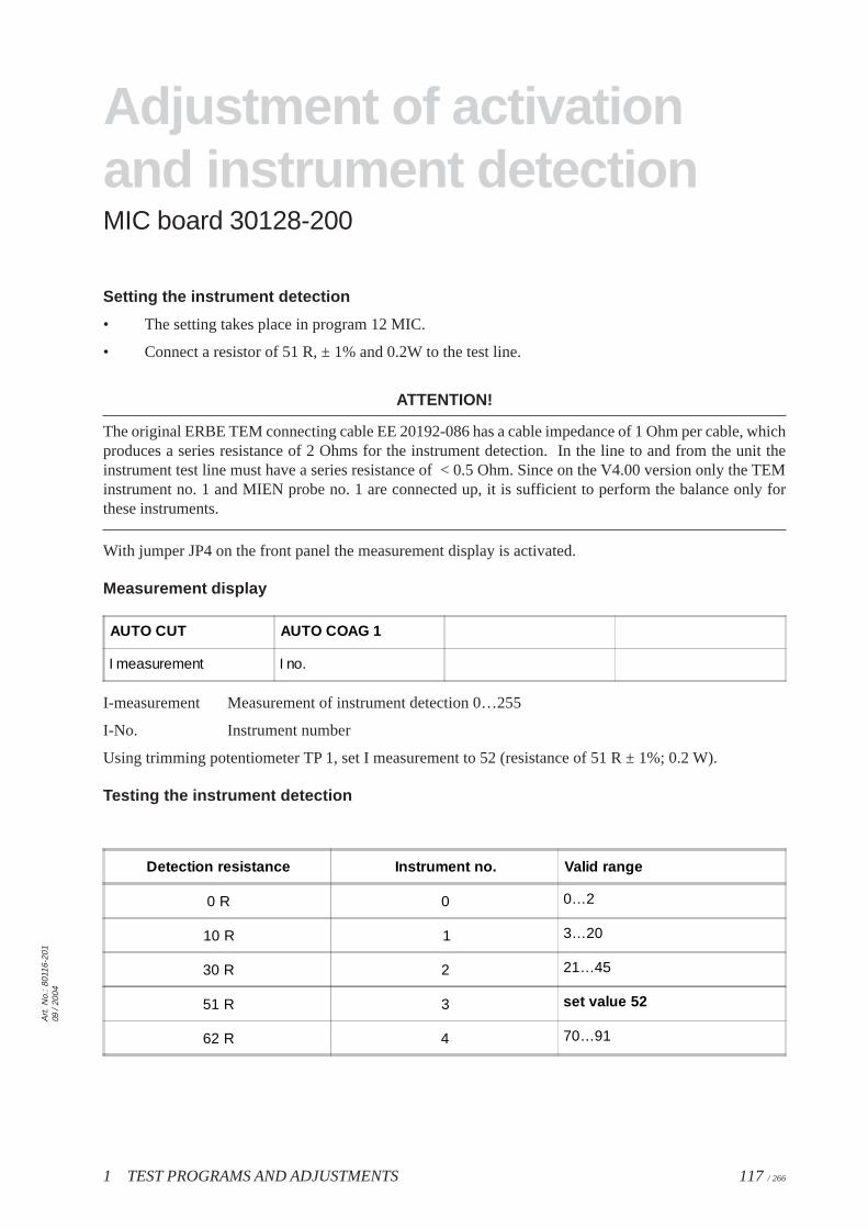
1 TEST PROGRAMS AND ADJUSTMENTS 117 / 266
Art
. No.
: 801
16-2
0109
/ 20
04
Adjustment of activationand instrument detectionMIC board 30128-200
Setting the instrument detection
• The setting takes place in program 12 MIC.
• Connect a resistor of 51 R, ± 1% and 0.2W to the test line.
ATTENTION!
The original ERBE TEM connecting cable EE 20192-086 has a cable impedance of 1 Ohm per cable, whichproduces a series resistance of 2 Ohms for the instrument detection. In the line to and from the unit theinstrument test line must have a series resistance of < 0.5 Ohm. Since on the V4.00 version only the TEMinstrument no. 1 and MIEN probe no. 1 are connected up, it is sufficient to perform the balance only forthese instruments.
With jumper JP4 on the front panel the measurement display is activated.
Measurement display
AUTO CUT AUTO COAG 1
I measurement I no.
I-measurement Measurement of instrument detection 0…255
I-No. Instrument number
Using trimming potentiometer TP 1, set I measurement to 52 (resistance of 51 R ± 1%; 0.2 W).
Testing the instrument detection
Detection resistance Instrument no. Valid range
0 R 0 0…2
10 R 1 3…20
30 R 2 21…45
51 R 3 set value 52
62 R 4 70…91
1 TEST PROGRAMS AND ADJUSTMENTS118 / 266
Adjustment of activationand instrument detectionMIC board 30128-200
Setting of activation detection
Set the trimming potentiometer TP 2 to approximately the center position.
ATTENTION!
Never forget to remove jumper JP4.
Test instructions for program 12 MIC
• Assignment of MIC output socket for the MIC program:
Pin 1: NE 1
Pin 2: NE 2 not assigned
Pin 3: CUT cutting function
Pin 4: Instrument detection between Pin 1 and Pin 4
Pin 5: Activation detection between Pin 1 and Pin 5
• Set and test instrument detection and activation detection:
Test instrument detection together with the TEM instrument EE 20191-275 and connecting cable EE20192-086 in the MIC program.
• Connect up the compressed air supply:
The MIC output socket is active in the MIC program. Connect up to the compressed air supply (max.5 bar). Connect up 10 Ohm detection resistor corresponding to TEM instrument no. 1.
• Test CUT function:
The CUT function is activated with the yellow footswitch.
MIC socket AUTO CUT APM P [Watt]
NE1CUT
Effect 340 W
500 Ohm 40 ± 15 %
ATTENTION!
The measuring system will be damaged beyond repair if the HF lines are connected up to the APM incorrectly.

1 TEST PROGRAMS AND ADJUSTMENTS 119 / 266
Art
. No.
: 801
16-2
0109
/ 20
04
Adjustment of activationand instrument detectionMIC board 30128-200
The output error display is activated at 40 W and 500 Ohm. Activation of the BIPOLAR CUT functionis also possible without the neutral electrode.
• Compressed air control
At instrument 1 the compressed air valve is opened during CUT activation. The compressed air valvecontrols the needle of the TEM instrument. After activation the needle reset time elapses. After needlereset time has elapsed the compressed air valve closes and the needle is reset. Needle reset time isindicated in test program 23. Check the compressed air valve to make sure that it operates properlyand to ensure there are no leaks.
• Check monopolar coagulation
Activation of the SOFT function and the FORCED function is performed using the blue footswitch.
MIC socket AUTO COAG 2 APM P [Watt]
NE1ICC 350 NE Electrode
SOFT 120 Watt 75 Ohm 120 ± 15 %
FORCED 60 Watt 350 Ohm 60 ± 15 %
Test instructions for program 13 MIEN
• Assignment of the MIC output socket for the MIEN program
Pin 1: NE 1 bipolar
Pin 2: CUT and COAG function bipolar. (MIEN protective circuit).
Pin 3: not assigned
Pin 4: Instrument detection between Pin 1 and Pin 4
Pin 5: Activation detection between Pin 1 and Pin 5
• Test instrument detection.
Test instrument detection together with the MIEN probe EE 20191-305/308 and handlepiece EE20191-306 in the MIEN program.
• Test bipolar CUT function
The CUT function is activated using the yellow footswitch.
ATTENTION!
The measuring system will be damaged beyond repair if the HF lines are connected up to the APM incorrectly.
1 TEST PROGRAMS AND ADJUSTMENTS120 / 266
Adjustment of activationand instrument detectionMIC board 30128-200
MIC socket AUTO COAG 2 APM P [Watt]
NE1 CUTEffect 315 Watt
500 Ohm 15 ± 3 (W)
The output error display is activated at 40 W and 500 Ohms. Activation of the bipolar CUT function is alsopossible without the neutral electrode.
• Test bipolar SOFT coagulation
The SOFT function is activated with the blue footswitch.
MIC socket AUTO COAG 2 APM P [Watt]
NE1 CUT SOFT 15 Watt500 Ohm
No-load voltage 84 ± 5 Vp
7 ± 2 (W)
• Test the protective circuit with test program 18
In the event of an error, the protective circuit in the MIEN program prevents an overdose of HFvoltage and HF current. If the output current is too high, the fusible link in the protective circuit trips.The test checks whether the correct fuse is inserted. The manufacturer of the fuse and the fuse ratingcan be found in the parts list.
• Testing the voltage limitation with no load
Activate test program 18.
In the AUTO CUT display panel the set value of HF output voltage is displayed. With the CUT “Up/Down” buttons, the HF output voltage can be adjusted in the range from 260Vp to 500 Vp (±50Vp).
Connect oscilloscope to the MIC output socket NE1 and CUT.
The highest HF peak voltage at the AUTO CUT Effect 3 (15 W) setting is 340 Vp. At this voltage the
protective circuit must not yet impose any limitation.
The protective circuit limits the output voltage from 360 Vp upward. Range in which the limitation
must be activated: 360–450 Vp.
At the setting of 499 Vp the fuse will not trip and the operability of the protective circuit remains
intact.
ATTENTION!
As soon as the voltage limitation is activated, current flows through the protective diodes and the diodes heatup. The duration of the test from the moment of voltage limitation must not exceed 5 seconds or else theprotective diodes break down and the circuit will have to be repaired.
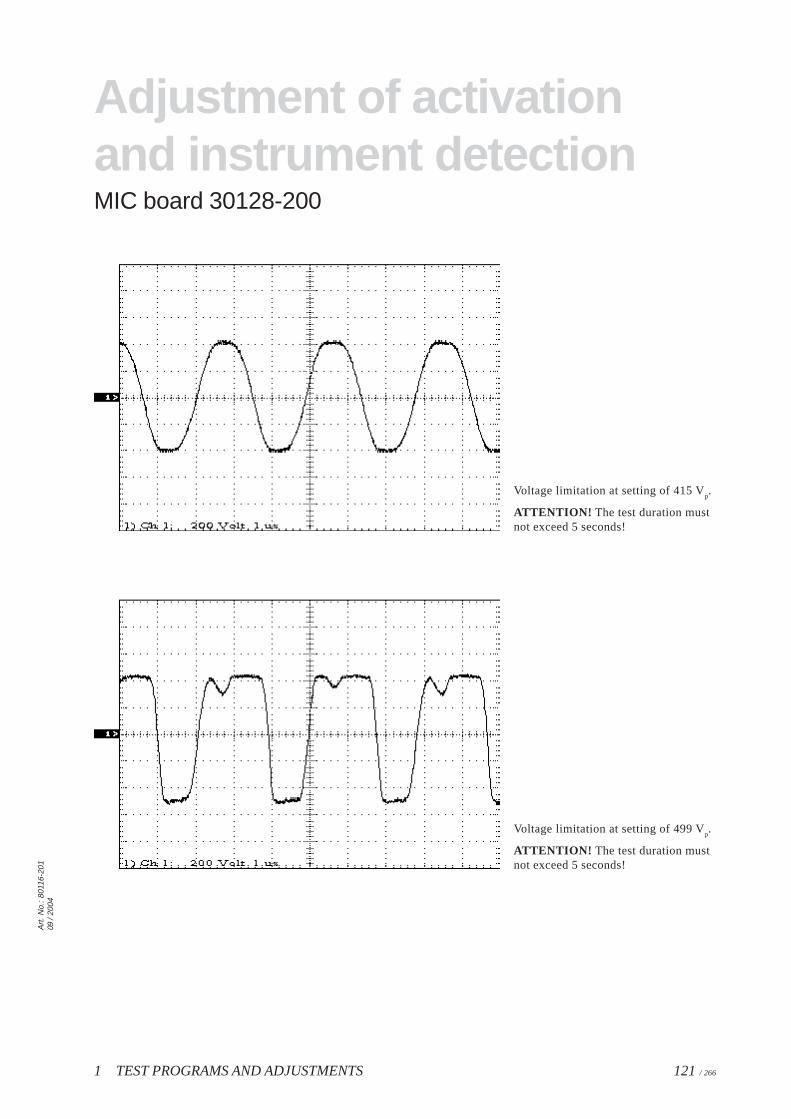
1 TEST PROGRAMS AND ADJUSTMENTS 121 / 266
Art
. No.
: 801
16-2
0109
/ 20
04
Adjustment of activationand instrument detectionMIC board 30128-200
Voltage limitation at setting of 415 Vp.
ATTENTION! The test duration mustnot exceed 5 seconds!
Voltage limitation at setting of 499 Vp.
ATTENTION! The test duration mustnot exceed 5 seconds!

1 TEST PROGRAMS AND ADJUSTMENTS122 / 266

1 TEST PROGRAMS AND ADJUSTMENTS 123 / 266
Art
. No.
: 801
16-2
0109
/ 20
04
Test program no. 17Brightness setting of the 7-segment displays
General description
Using this program, you can adapt the brightness of the 7-segment displays in 10 stages to the lightingconditions of the room.
After starting the test program, you will see the following display:
AUTO CUT AUTO COAG 1 AUTO COAG 2 AUTO BIPOLAR
Int xx
• Int Intensity (brightness) of the displays
• xx Present intensity, adjustable from 1...10.
You can make the intensity brighter using the “Up” (8) key or darker using the “Down” (9) key.
After termination of the test program, store the brightness setting with key 3.

1 TEST PROGRAMS AND ADJUSTMENTS124 / 266
Test program no. 23Changing the delay time withAUTO START
General description
Using this program, you can change the specifications for the delay time when activating AUTO START.
The delay time is the time which passes after the forceps contacted the tissue and the HF generator isactuated.
So that the operating surgeon can know whether the forceps have contacted the tissue, the AUTO BIPO-LAR activation display (blue triangle in the AUTO-BIPOLAR field) switches on at contact. Then the delaytime starts. After the delay time has passed, the HF generator and the activation tone are switched on.
In case of error in the memory medium, the following basic settings have been preset:
ICC 350 and ICC 300: AUTO START 0: 0 seconds,
AUTO START 1: 0.5 seconds,
AUTO START 2: 1 second;
ICC 200: AUTO START: 0.5 seconds.
After starting Test program 23, you will see the following display:
AUTO CUT AUTO COAG 1 AUTO COAG 2 AUTO BIPOLAR
SEt Up tt.t
Time setting
Possible from 0.1 to 10 seconds in the following time steps:
from 0.1 to 2.0 seconds in 0.1 seconds steps
from 2.0 to 10.0 seconds in 0.5 seconds steps.
Procedure for ICC 350
AUTO START Setting range
0 0 greater than/equal to t greater than/equal to 1
1 1 greater than/equal to t greater than/equal to 2
2 2 greater than/equal to t greater than/equal to 10 seconds
You can set and store the delay time for every user-specific program 0 to 9 and for every AUTO-STARTtime (0, 1 and 2).
Since the AUTO-START time 0 can be no longer than AUTO-START time 1, it is best to proceed from thelongest time for AUTO START 2 and then set the times for AUTO START 1 and AUTO START 0.

1 TEST PROGRAMS AND ADJUSTMENTS 125 / 266
Art
. No.
: 801
16-2
0109
/ 20
04
NOTE
You will find the assignment of keys with the numbers given below on pages 1-4 (Calling up of the testprogram mode) of this Service Manual.
1. Using key 2 Set program number
2. Using key 14 Set AUTO START 2
3. Using “Up” or “Down” key Set the required time
4. Using key 14 Set AUTO START 1
5. Using “Up” or “Down” key Set the required time
6. Using key 14 Set AUTO START 0
7. Using the “Up” or “Down” key Set the required time
8. Using key 1 Store the set values.
Steps 1 to 8 can be repeated individually for every required program.
Then exit the test program using key 3.
Procedure for ICC 300
AUTO START Setting range
0 0 greater than/equal to t greater than/equal to 1
1 1 greater than/equal to t greater than/equal to 2
2 2 greater than/equal to t greater than/equal to 10 seconds
For every AUTO START time (0, 1 and 2), you can set and store a delay time. Since the AUTO-START time0 cannot be any longer than the AUTO-START time 1, it is best to proceed from the longest time for AUTOSTART 2 and then set the times for AUTO START 1 and AUTO START 0.
1. Using key 14 Set AUTO START 2
2. Using the “Up” or “Down” key Set the required time
3. Using key 14 Set AUTO START 1
4. Using the “Up” or “Down” key Set the required time
5. Using key 14 Set AUTO START 0
6. Using the “Up” or “Down” key Set the required time
7. Using key 3 Exit the test program and the set valuesare stored.
Test program no. 23Changing the delay time forAUTO START

1 TEST PROGRAMS AND ADJUSTMENTS126 / 266
Procedure for ICC 200
AUTO CUT AUTO COAG 1 AUTO COAG 2 AUTO BIPOLAR
SEt Up tt.t
For the AUTO START function, you can set and store a delay time.
1. Using the “Up” or “Down” key Set the required time
2. Using key 3 The set values are stored and the test program isexited.
Test program no. 23Changing the delay time forAUTO START

Chapter 2ERROR list

2 ERROR LIST 129 / 266
Art
. No.
: 801
16-2
0109
/ 20
04
ERROR list V 4.XERBOTOM ICC 350 (V4.0, V2.0), ICC 300 (V3.0),ICC 200 (V2.0)
Automatic error detection, indication and documentation
ERBOTOM ICC series high-frequency surgical units are equipped with a device for automatic error detection,indication and documentation (ERROR monitor).
Error detection, indication, documentation
For ERBOTOM ICC series equipment as of software version 2.0 / 4.0, the ERROR monitor can, dependingon the type of equipment and its outfit, detect up to 91 currently occurring errors (ERROR) and indicate themon the display.
Error numbers (ERROR nos.) are assigned to the various errors. If an error is detected, it is immediatelyreported. The error report is both visual and audible.
The error numbers of detected errors are automatically stored chronologically. Since only 10 memory locationsare available, only the last 10 error messages are displayed. If the same error is detected several times in a row,the corresponding error number is then saved only once in consideration of the limited number of availablememory locations. The error numbers documented in memory can be displayed via Test program 2 anddeleted.
Troubleshooting for ICC family equipment
The ICC unit family is equipped with an error detection system which detects and stores the last 10 errorsdetected in an ERROR list. This error memory can be called up via Test program no. 2. The user should thusbe capable of localizing errors himself and deciding whether this is an operating error or an error in theaccessories, which he can possibly eliminate himself, or whether it is necessary to make use of the technicalservice.
If there is a complete failure of the system and no display is visible, the power supply may have beeninterrupted or the voltage supply inside the unit is defective. In such a case, first check whether the outletused is live or a fuse in the house power supply has been tripped (Does a different unit function at thisoutlet?). If the outlet used is live, check the powerline to the unit and replace if necessary. The equipmentfuses on the rear panel should also be checked and replaced if necessary.
ATTENTION!
Only use original fuses of the same specification.
If these efforts bring no results, there is probably an error within the unit. You should then contact thetechnical service.
For a malfunction with a properly functioning display but with no indication of an ERROR number in thedisplay, the error may be located in defective accessories. It is possible, for example, that there may be adefect in the fingerswitch or footswitch, or a disruption in the associated connecting cable. The cause of theerror may be determined by exchanging the accessories used.
To determine other causes of errors, an ERROR number in the unit display indicates the course of furtheraction according to the following table.
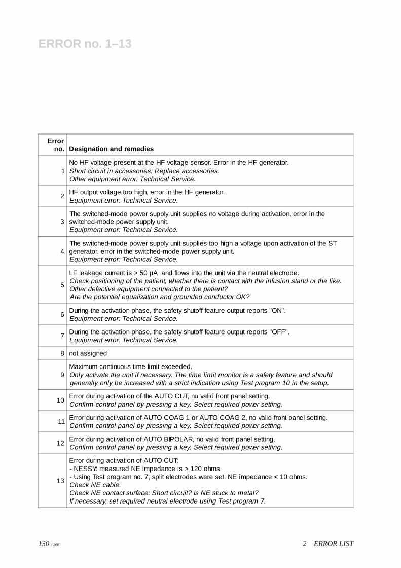
2 ERROR LIST130 / 266
ERROR no. 1–13
Errorno. Designation and remedies
1No HF voltage present at the HF voltage sensor. Error in the HF generator.Short circuit in accessories: Replace accessories.Other equipment error: Technical Service.
2HF output voltage too high, error in the HF generator.Equipment error: Technical Service.
3The switched-mode power supply unit supplies no voltage during activation, error in theswitched-mode power supply unit.Equipment error: Technical Service.
4The switched-mode power supply unit supplies too high a voltage upon activation of the STgenerator, error in the switched-mode power supply unit.Equipment error: Technical Service.
5
LF leakage current is > 50 µA and flows into the unit via the neutral electrode.Check positioning of the patient, whether there is contact with the infusion stand or the like.Other defective equipment connected to the patient?Are the potential equalization and grounded conductor OK?
6During the activation phase, the safety shutoff feature output reports "ON".Equipment error: Technical Service.
7During the activation phase, the safety shutoff feature output reports "OFF".Equipment error: Technical Service.
8 not assigned
9Maximum continuous time limit exceeded.Only activate the unit if necessary. The time limit monitor is a safety feature and shouldgenerally only be increased with a strict indication using Test program 10 in the setup.
10Error during activation of the AUTO CUT, no valid front panel setting.Confirm control panel by pressing a key. Select required power setting.
11Error during activation of AUTO COAG 1 or AUTO COAG 2, no valid front panel setting.Confirm control panel by pressing a key. Select required power setting.
12Error during activation of AUTO BIPOLAR, no valid front panel setting.Confirm control panel by pressing a key. Select required power setting.
13
Error during activation of AUTO CUT:- NESSY: measured NE impedance is > 120 ohms.- Using Test program no. 7, split electrodes were set: NE impedance < 10 ohms.Check NE cable.Check NE contact surface: Short circuit? Is NE stuck to metal?If necessary, set required neutral electrode using Test program 7.
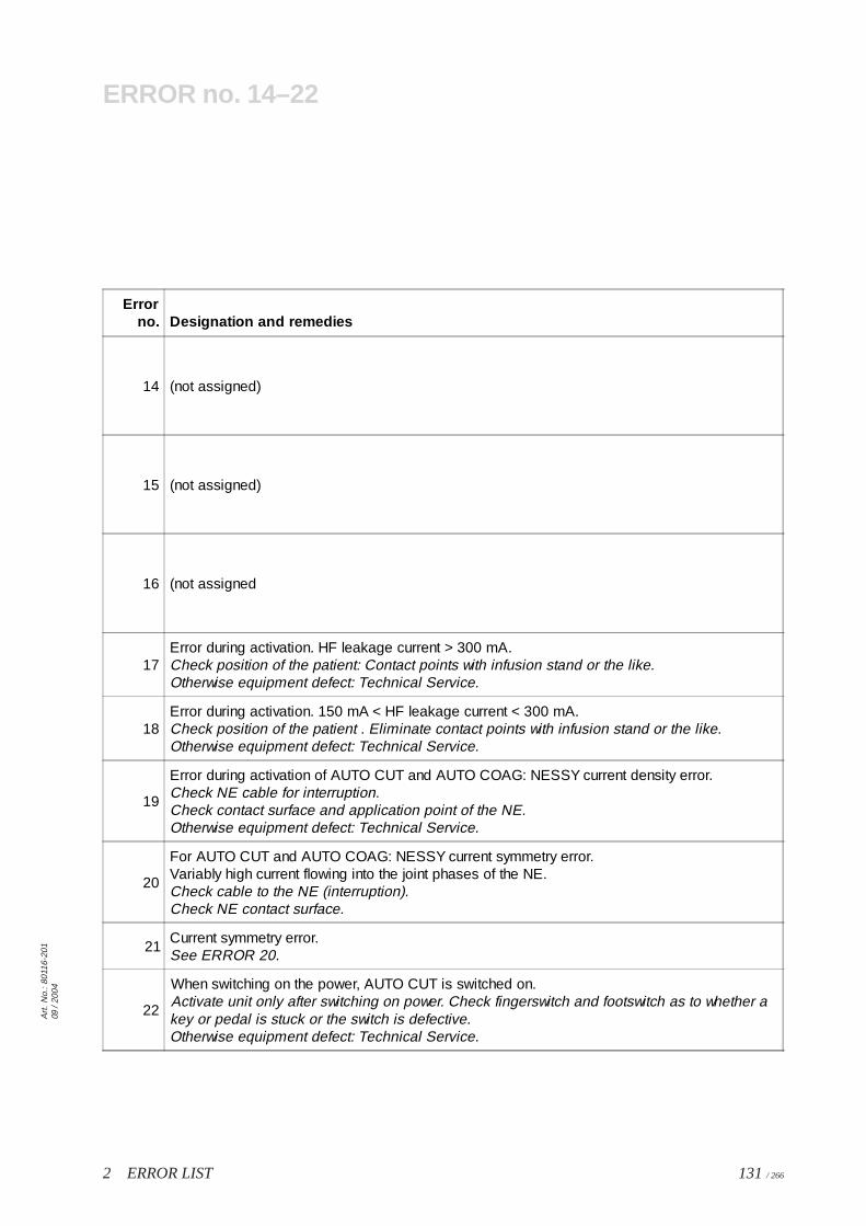
2 ERROR LIST 131 / 266
Art
. No.
: 801
16-2
0109
/ 20
04
ERROR no. 14–22
Errorno. Designation and remedies
14 (not assigned)
15 (not assigned)
16 (not assigned
17Error during activation. HF leakage current > 300 mA.Check position of the patient: Contact points with infusion stand or the like.Otherwise equipment defect: Technical Service.
18Error during activation. 150 mA < HF leakage current < 300 mA.Check position of the patient . Eliminate contact points with infusion stand or the like.Otherwise equipment defect: Technical Service.
19
Error during activation of AUTO CUT and AUTO COAG: NESSY current density error.Check NE cable for interruption.Check contact surface and application point of the NE.Otherwise equipment defect: Technical Service.
20
For AUTO CUT and AUTO COAG: NESSY current symmetry error.Variably high current flowing into the joint phases of the NE.Check cable to the NE (interruption).Check NE contact surface.
21Current symmetry error.See ERROR 20.
22
When switching on the power, AUTO CUT is switched on.Activate unit only after switching on power. Check fingerswitch and footswitch as to whether akey or pedal is stuck or the switch is defective.Otherwise equipment defect: Technical Service.
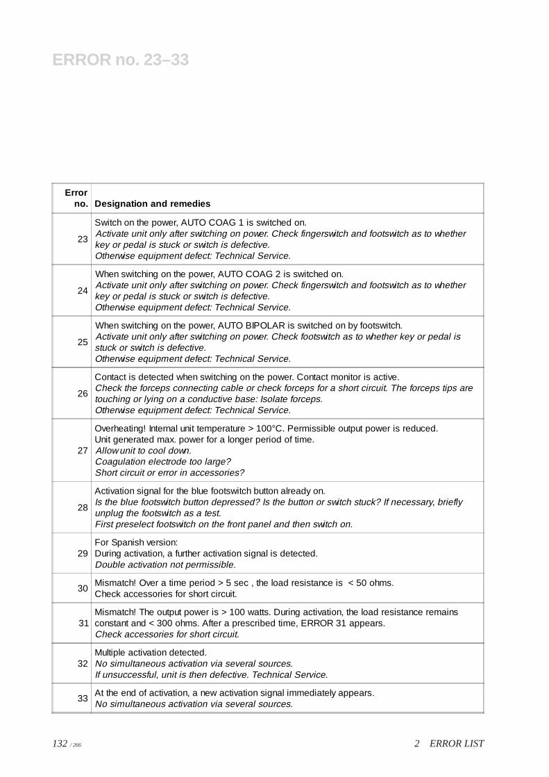
2 ERROR LIST132 / 266
ERROR no. 23–33
Errorno. Designation and remedies
23
Switch on the power, AUTO COAG 1 is switched on.Activate unit only after switching on power. Check fingerswitch and footswitch as to whetherkey or pedal is stuck or switch is defective.Otherwise equipment defect: Technical Service.
24
When switching on the power, AUTO COAG 2 is switched on.Activate unit only after switching on power. Check fingerswitch and footswitch as to whetherkey or pedal is stuck or switch is defective.Otherwise equipment defect: Technical Service.
25
When switching on the power, AUTO BIPOLAR is switched on by footswitch.Activate unit only after switching on power. Check footswitch as to whether key or pedal isstuck or switch is defective.Otherwise equipment defect: Technical Service.
26
Contact is detected when switching on the power. Contact monitor is active.Check the forceps connecting cable or check forceps for a short circuit. The forceps tips aretouching or lying on a conductive base: Isolate forceps.Otherwise equipment defect: Technical Service.
27
Overheating! Internal unit temperature > 100°C. Permissible output power is reduced.Unit generated max. power for a longer period of time.Allow unit to cool down.Coagulation electrode too large?Short circuit or error in accessories?
28
Activation signal for the blue footswitch button already on.Is the blue footswitch button depressed? Is the button or switch stuck? If necessary, brieflyunplug the footswitch as a test.First preselect footswitch on the front panel and then switch on.
29For Spanish version:During activation, a further activation signal is detected.Double activation not permissible.
30Mismatch! Over a time period > 5 sec , the load resistance is < 50 ohms.Check accessories for short circuit.
31Mismatch! The output power is > 100 watts. During activation, the load resistance remainsconstant and < 300 ohms. After a prescribed time, ERROR 31 appears.Check accessories for short circuit.
32Multiple activation detected.No simultaneous activation via several sources.If unsuccessful, unit is then defective. Technical Service.
33At the end of activation, a new activation signal immediately appears.No simultaneous activation via several sources.
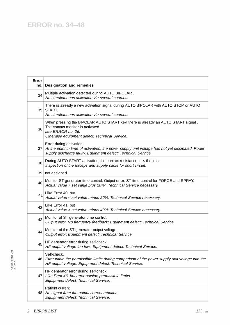
2 ERROR LIST 133 / 266
Art
. No.
: 801
16-2
0109
/ 20
04
ERROR no. 34–48
Errorno. Designation and remedies
34Multiple activation detected during AUTO BIPOLAR .No simultaneous activation via several sources.
35There is already a new activation signal during AUTO BIPOLAR with AUTO STOP or AUTOSTART.No simultaneous activation via several sources.
36
When pressing the BIPOLAR AUTO START key, there is already an AUTO START signal .The contact monitor is activated.see ERROR no. 26.Otherwise equipment defect: Technical Service.
37Error during activation.At the point in time of activation, the power supply unit voltage has not yet dissipated. Powersupply discharge faulty. Equipment defect: Technical Service.
38During AUTO START activation, the contact resistance is < 6 ohms.Inspection of the forceps and supply cable for short circuit.
39 not assigned
40Monitor ST generator time control. Output error: ST time control for FORCE and SPRAY.Actual value > set value plus 20%: Technical Service necessary.
41Like Error 40, butActual value < set value minus 20%: Technical Service necessary.
42Like Error 41, butActual value > set value minus 40%: Technical Service necessary.
43Monitor of ST generator time control.Output error. No frequency feedback: Equipment defect: Technical Service.
44Monitor of the ST generator output voltage.Output error: Equipment defect: Technical Service.
45HF generator error during self-check.HF output voltage too low : Equipment defect: Technical Service.
46Self-check.Error within the permissible limits during comparison of the power supply unit voltage with theHF output voltage. Equipment defect: Technical Service.
47HF generator error during self-check.Like Error 46, but error outside permissible limits.Equipment defect: Technical Service.
48Patient current.No signal from the output current monitor.Equipment defect: Technical Service.

2 ERROR LIST134 / 266
ERROR no. 49–82
Errorno. Designation and remedies
49 not assigned
50to 70
A key on the front panel is depressed.Operating field key is depressed or defective during the power start-up phase. If it cannot becorrected, then equipment defect: Technical Service.
71Interface error for ICC 350 DOKU: Start or stop bit error or number of bits incorrect.Equipment defect: Technical Service.
72Interface error for ICC 350 DOKU: Signal in receiving register has not been read out.Equipment defect: Technical Service.
73Interface error for ICC 350 DOKU: Parity sign placed incorrectly.Equipment defect: Technical Service.
74Interface error for ICC 350 DOKU: No connection to PC available.Equipment defect: Technical Service.
75Interface error for ICC 350 DOKU: Sign stays in transmitter buffer. SIO module not transmitting.Equipment defect: Technical Service.
76Interface error for ICC 350 DOKU: Interface storage takes too long; hard disk is too slow.Equipment defect: Technical Service.
77to 79
not assigned
80ICC 350 NEUROTEST: No valid frequency for the 5-stage intensity setting.Replace remote control.Otherwise equipment defect: Technical Service.
81ICC 350 NEUROTEST: The intensity setting was set to 0 during activation.Do not set anything during activation.Otherwise equipment defect: Technical Service.
82ICC 350 NEUROTEST: NESSY measurement: NE impedance > 120 ohms.Test the neutral electrode and supply line or position of the NE on the patient.Otherwise equipment defect: Technical Service.

2 ERROR LIST 135/ 266
Art
. No.
: 801
16-2
0109
/ 20
04
ERROR no. 83–91
Errorno. Designation and remedies
83ICC 350 NEUROTEST: Output current too high, but still within the permissible limits.Equipment defect: Technical Service.
84ICC 350 NEUROTEST: Output current too high; outside permissible limits.Equipment defect: Technical Service.
85
ICC 350 NEUROTEST: No output current. Interruption of the circuit or failure of the frequencyfeedback system.Check the neurotest cable supply lines or the handle, NE and cable and replace ifnecessary.Otherwise equipment defect: Technical Service.
86
ICC 350 NEUROTEST: Output current too low, but within the permissible limits.Check the neurotest cable supply lines, or the handle, NE and cable, and replace ifnecessary.Otherwise equipment defect: Technical Service.
87ICC 350 NEUROTEST: Output current too low; current is below the permissible limit.Check neurotest cable.Otherwise equipment defect: Technical Service.
88ICC 350 NEUROTEST: Max. time limit has run out. The time limit monitor is a safety measure.Only activate unit if necessary.
89ICC 350 NEUROTEST: When switching on the power, already a neurotest activation signal.Equipment defect: Technical Service.
90ICC 350 NEUROTEST: Electronic fuse triggered or frequency feedback system has failed.Equipment defect: Technical Service.
91
ICC 350 NEUROTEST: After switching on the neurotest function using the intensity adjuster, atest determined that the electronic fuse was not triggered or the frequency feedback systemhas failed.Equipment defect: Technical Service.

2 ERROR LIST136 / 266

Chapter 3Circuit description


139 / 2663 CIRCUIT DESCRIPTION
Art
. No.
: 801
16-2
0109
/ 20
04
Motherboard
The following functions are also found on the motherboard:
• Starting current limitation
• Supply voltage changeover and power rectification
• Power transformer for low voltage supply
• Rectifier for low voltage
• Chipselect generation and level adaptation of TTL level to 15 volt level for CMOS components.
• Generation of the external control bus and of signal lines from the data from PIO outputs
• HF leakage current measurement
• HF leakage current limitation
• Changeover between floating and capacitance-grounded output
• Input circuit for the footswitch
• Various level adaptations.
The motherboard detects the other PCBs via connectors and contacts them.
Starting current limitation
The supply voltage moves from the power supply to the motherboard via the connector J 11.
Immediately after switching on the ICC, the supply unit capacitors are charged which causes a heavypower surge by which, without protective measures, the fuses for the in-house electrical system would betriggered.
Therefore a starting current limitation has been realized on the motherboard which limits the current peakto noncritical values after switching on.
The corresponding power current first flows into the ICC via the resistor R5 and the fuse F1. The relaycontacts REL 1 are still briefly opened. Power current is therefore temporarily limited to noncritical valuesdue to resistor R5.
As soon as the 24 volt supply voltage is available, relay REL 1 can pick up, bridges resistor R5 and fuse F1with its relay contacts, and relieves both of them. This short span of time is sufficient to effectively limit thestarting power surge.
LED D2 lights red when the relay REL 1 is actuated and thus serves as a control.
Supply voltage switchover and power rectification
The unit can be changed over either to the 230 volt or 115 volt supply voltage range. The remaining voltagedeviations within the specification are offset by the controlled power supply units.
The supply voltage can be switched over by shifting the connectors J 16 to J 22.
In the 230 volt range, the bridge-connected rectifier BR1 functions as intended as a true bridge circuit. Thewire bridges must be connected as follows:

140 / 266 3 CIRCUIT DESCRIPTION
J 15 free
J 16–J 20 grey
J 17–J 21 brown
J 18–J 22 yellow
J 19 free
In the 115 volt range, the bridge-connected rectifier BR1 operates with the electrolyte capacitors C6, C7 asa voltage doubler. The wire bridges must be connected as follows:
J 15–J 20 grey
J 16 free
J 17 free
J 18–J 21 brown
J 19–J 22 yellow
For the low voltage supply, there is a transformer TR 1 with rectifier BR2 and filter capacitor C15 on themotherboard. Here an unregulated DC voltage is provided in the 24 volt range.
Since data are present on the databus for all parts of the circuit simultaneously, it is necessary to separatelydetermine for which part of the circuit the currently output data is intended. This is realized by the “Chipselectmethod” by which the chip to be addressed is selected and addressed using a special “Chipselect signal.”
This signal activates only one among a number of addressable modules. These signals are generated withinthe Multiplexer IC 4 and converted in the transistor arrays IC10 and IC11 to 15 volt CMOS level.
The PIO (Parallel Input Output module) produces data in a brief period of time for many different targetassemblies. While the data are only present briefly at the PIOs, the data for target assemblies should bepresent longer. For this an independent external control bus and independent control lines are used. Thedata for the signal lines are stored in the D-flipflops IC2 and IC3 and brought to the 15 volt CMOS level inthe transistor arrays IC8 and IC9.
For the external control bus, the PIO data only need to be brought to the 15 volt CMOS level in IC7.
Limitation of the high frequency leakage currents
High frequency leakage currents are effectively limited in the ICC. The transformer UE1 is used for limitation.
All lines which lead to a high-frequency output socket on the ICC are directed via transformer UE1. If nohigh frequency leakage currents occur, the HF current flows from the generator via the patient to the neutralelectrode and via the transformer UE1 back to the generator completely.
Therefore ideally, the current flowing away is equal to the current flowing back. The windings of thetransformer UE1 are switched in such a way that the resulting magnetic field is canceled by the currentflowing back and forth. Thus the windings of this transformer have no inductivity; the current can flowunimpeded.
However, if high-frequency leakage currents do occur within the patient circuit, the current flowing backand forth is generally not equal. The magnetic fields in the transformer UE1 do not cancel each other out;
Motherboard
141 / 2663 CIRCUIT DESCRIPTION
Art
. No.
: 801
16-2
0109
/ 20
04
an inductivity of the coils results which limits the high-frequency leakage current with this inductiveimpedance.
Monitoring the high-frequency leakage currents
As intended, the high-frequency current should only be used for cutting or coagulating tissue. To do this, itmust flow to the active electrode in a small area and with a high current density, and flow back again fromthe neutral electrode over a large area and with a low current density.
However, if the body of the patient is in contact with another electrically conductive object, the current mayalso take an undesirable path and, for example, cause a burn there. These undesirable currents are known as“leakage currents”. It is therefore important to know whether such a leakage current is flowing and howlarge it is.
Such leakage current cannot simply disappear, but must instead always flow back to the generator. Thelargest proportion of these high-frequency leakage currents flow back to the generator via the power cableand the grounded conductor.
Since all power lines and the grounded conductor are directed through the ring core of the coil L1, acorresponding high frequency voltage is induced if HF leakage current is present in the coil L1, which isrectified with diode D1, restricted with D6, D7 and smoothed in capacitor C13. For further processing, thisDC voltage is fed to the processor system via the isolation amplifier IC12.
Changeover between flowing and capacitance-grounded output
High-frequency surgical units are generally available either in “capacitance ground of the neutral electrode”or “floating neutral electrode” connection systems, whereby no components are integrated between theconnection to the neutral electrode and chassis in the latter connection system.
Both connection systems have advantages and disadvantages.
The advantage of capacitance ground is that the feed line from the neutral electrode to the patient is groundedat a high frequency via the capacitor and the risk of burns is reduced. However, it is a disadvantage thatimpermissible low-frequency leakage currents may flow through this capacitor during cardiac operations.
If the neutral electrode is operated as floating, on the other hand, the low-frequency leakage currents can bekept very easily below the limit value of 10 or 50 mA during cardiac operations, but the risk of burns isincreased in this connection system since the line from the neutral electrode is about half the high frequencyvoltage of the generator.
With the ICC high-frequency surgical units, the low-frequency leakage current to the patient is measured.At the first malfunction, this must not exceed 50 mA. Once this condition is ensured, the unit is permittedto carry the CF designation (Cardiac Floating). If the possible low-frequency leakage current is under 500mA in the first case of malfunction, the unit is therefore not suitable for operations on the heart and has thedesignation BF (Body Floating).
Initially the ICC is capacitance-grounded via capacitors C30 and C31 and the relay contact REL 2. Theadvantages of capacitance ground are fully exploited. The low-frequency leakage current is measured viathe prescribed simulation R25, C28. If for any reason a low-frequency leakage current should appear, it isthen evaluated. If it exceeds the limit of 50 mA, the relay contacts REL 2 are then opened and thus a low-frequency leakage current can no longer flow. The ICC thus fulfills the CF requirement for cardiac surgery
Motherboard

142 / 266 3 CIRCUIT DESCRIPTION
in every situation.
The voltage occurring in the simulation is proportional to the current and is compared in the operationamplifier IC14 functioning as a comparator to the maximum permissible value that is prescribed andadjustable via the resistor divider R22 and TP1. The signal for switching over the relay REL 2 is present atthe BF / CF output.
Footswitch input circuit
The footswitch is operated at a DC voltage of 15 volts via a multipole line. Since the footswitch connection,due to its length of up to several meters, can also function as a receiving antenna and absorb interferences,an RC low-pass is connected directly to the input sockets of the ICC which severely dampens high interferencefrequencies. The footswitch signals are then regenerated using the buffer IC 13.
For further processing in the processor, the output signals from IC 13 are adapted to the TTL level of theprocessor. To do this, the noninverting buffer IC5 is used.
Further signals are converted in the same manner from 15 volt CMOS level to the TTL level in the buffersIC1 and IC6.
Motherboard
143 / 2663 CIRCUIT DESCRIPTION
Art
. No.
: 801
16-2
0109
/ 20
04
CPU boardSlot J1
The following functions are located on the PCB:
• The CPU with RAM and EPROM
• The clock generator
• The voltage supply monitor
• The digital input and output via Parallel Input/Output modules (PIO)
• Analog inputs via an A/D converter
• The Chipselect generation
• The safety interlock signal for controlling the activation signals.
As the central processing unit (CPU), the CMOS microprocessor Z84 C00 (IC1) is used together with theEPROM 27 C 512 as the program memory (IC3) and the battery-buffered RAM 5864 as the main memoryand constant memory (IC2)
The clock pulse for operation of the computer is produced in the quartz clock generator IC16 and then processedin the two D-flipflops IC13 to a half-frequency, counterphase clock.
In case of a breakdown of the supply voltage, the current computer data must still be “saved” and stored in thebattery-buffered RAM. All these tasks are supported by the supervisor circuit IC10 (MAX 691).
The supply voltage is monitored via the resistor voltage divider R3, R4 and the “Powerfail” input (Pin 9,IC10). The data are buffered by a 3 volt lithium battery BT1 which is connected at Pin 1 of the IC10. Thecircuit also monitors the voltage of this buffer battery. When switching on, the circuit affects a reset of thecomputer system to a specific initial status and provides the monitoring and functional capability through anintegrated “watchdog” circuit.
In addition, the +5 volt supply voltage is also monitored in a separate circuit via resistor R9, diode D1, buffercapacitor C13 and resistor R7 via the PIO IC6, Pin 27.
The digital inputs and outputs of the computer are taken care of by the Parallel Input/Output circuits (PIOs,IC4 to IC7). The input and output ports are specified and connected by the program.
Analog dimensions, processed by the processor, move via the level adaptation (resistor network RN1, resistorsR15 to R18) and simultaneous low-pass (capacitors C16 to C19) to the 4-channel analog-digital converterIC14, from whence the data are available to the processor.
Since all system data are present together at the databus, the system must be able to address the target modulesto which the data apply. This occurs in a processor system by means of the Chipselect lines by which veryspecific modules can be addressed via the assistance of “selection signals”.
The Chipselect signals are created in the decoder IC9 from the addresses A3, A4 and A5. Depending on theaddress, only one output line each is switched to logical low.
All signals from the various fingerswitches and footswitches are summarized and verified in a safety interlocksignal as to whether any impermissible overlappings or impermissible conditions are produced. If noimpermissible overlappings are determined, the safety interlock signal generates a signal which identifies thepassed on data as save. This logic is accepted by the programmable controller IC17.
144/ 266 3 CIRCUIT DESCRIPTION
Low voltage supplySlot J2
The following assemblies are located on the PCB:
• Voltage regulator for +24 volts
• Voltage regulator for +15 volts
• Voltage regulator for +5 volts
• Voltage regulator for –15 volts
• Three sound generators for the acoustic signals
• Circuit for tone selection
• Tone output amplifier with volume control.
Voltage regulator for +24 volts
The unstabilized DC voltage, gained on the motherboard via transformer TR1 and bridge-connected rectifierBR2, moves to the input of a switched-mode power supply unit. This consists of the integrated switchingcontroller IC3, the memory choke L1 and the free-wheeling diode D1 with the necessary wiring. Theoutput voltage is adjusted via the voltage divider R22, R23.
At the output of the switching controller, a stabilized DC voltage of +24 volts is available. The presence ofthis voltage is indicated by the LED6.
This voltage is mainly used to operate the relays in the surgical unit.
Voltage regulation for +15 volts
The instable input voltage, the presence of which is indicated by LED 4, moves to the switchingcontroller IC 1. The circuit extensively corresponds to the +24 volt regulation, however the transformerUE 1 is used here as the memory choke which simultaneously taps a part of the connector voltageoccurring there for the operation of the – 15 volt regulation.
The output voltage of 15 volts prescribed by the divider ratio of the resistors R30 and R31 is used tooperate the CMOS circuits and the operation amplifier. Its proper presence is signaled by the LED 2.
Voltage regulation for – 15 volts
The negative operation voltage of – 15 volts is mainly required for the negative voltage supply of theoperation amplifier. Since the capacity of this voltage source is just minimal due to the circuit, a simpleregulating circuit could be used. The principle of analog regulation is thus sufficient, and the resultinglosses are minimal.
The switched-mode voltage tapped from the switched-mode power unit for + 15 volts at transformer UE 1is rectified through the diode D6 such that a negative DC voltage is present at the input of the analogregulator IC10. This voltage is stabilized by the fixed voltage controller IC10 to –15 volts. The properpresence of this voltage is indicated by the LED1.

145 / 2663 CIRCUIT DESCRIPTION
Art
. No.
: 801
16-2
0109
/ 20
04
Voltage regulation for +5 volts
A controlled voltage of +5 volts is mainly required to operate the CPU, the TTL logic modules and the lightdisplays on the front panel. Since the capacity of this voltage source is relatively high, a switched-modepower supply unit was used.
The circuit corresponds extensively to that of the +24 volt regulator: The instable input voltage is stabilizedto +5 volts by means of the regulator IC6. The proper presence of the output voltage is indicated by theLED3.
From Pin 3 of the integrated switching controller IC1 of the +15 volt voltage regulation, a connection leadsto the transistor T2 of the +5 volt control. In this way it is possible to block the function of the +5 volt powersupply unit as long as the +15 volt supply is not available. This measure is used to increase the functionalsecurity of the unit.
Tone generators for the signal tones
The tone generators are used to audibly signal all operating and danger conditions when operating thesurgical unit. To do this, three tone generators are available, the signals of which may be mixed with oneanother to produce pleasant and differing tones in this way.
The timer IC4 produces the tone frequency for the first tone, which can be adjusted using the trimpotentiometer TP2 at 493 Hz.
Timer IC5 produces the tone frequency for the second tone, which can be adjusted using the trimpotentiometer TP3 at 414 Hz.
Timer IC7 produces the tone frequency for the third tone, which can be adjusted using the trim potentiometerTP4 at 329 Hz.
The generated tone frequencies can now be switched on selectively using the analog switches on the IC8and mixed with one another. The combination of individual tones is prescribed by the program and isselected using the D-flipflops of the IC9 as a target memory and switched through using the analog switchesof the IC8. Via resistors R5, R7, R9, R24, R10 and R16, the tone frequencies are combined so that onesound can result from several individual frequencies.
The volume of the operating tones can be adjusted using a potentiometer which is connected in parallel toresistor R11.
The volume of the alarms must not be reduced. For this reason, the reduction of amplitudes by means of theintegrated analog switch IC8, Pin 10-11, which is also controlled by the CPU, can be passed by so that thetone signal in this case is reproduced with the maximum amplitude at the tone output amplifier IC 2.
The R37, C9, C10, C11, R39 network is used for sound shaping, so that a pleasant sound results in theloudspeaker which follows the tone amplifier.
Low voltage supplySlot J2
146 / 266 3 CIRCUIT DESCRIPTION
The following assemblies are found on the PCB:
• Measured value acquisition and adjustment
• The contact monitor
• Actuation and power setting of the ST output stage
• Actuation of the power module
• Synchronization of the QK output stage
• Hardware electronic safety circuits
• Spark control
• Actuation of the QK output stage.
Measured value acquisition and adjustment
The measurement signals, which are triggered mainly to the Senso-board as well as to other parts of theentire unit, move first to the control board where they usually must still be adjusted in order to finally moveon to the processor.
For most inputs, an input circuit consists of a variable voltage divider with which the signal voltages can be adjusted.
Various signal voltages, the values of which are needed very quickly by the processor system, proceed viathe amplifiers IC1 and IC2 directly to the processor. (See diagram page 2/3).
Other signals which are not required for fast processing can be fed to the processor system in multiplexoperation. (Circuit diagram page 3/3). These signals are fed to the 16-channel multiplex IC 3, scanned inchronological order, then amplified in the operation amplifier IC1 and only then fed one after another to theprocessor system (output ANALOG 4).
The individual operating voltages, for example, are determined in this way:
The +15 volt operating voltage is fed via the resistor divider R39, R40 to the multiplexer.
The +24 volt operating voltage is fed via the resistor divider R41, R42 to the multiplexer.
The –15 volt operating voltage is first fed via R31 to the operation amplifier IC2 by inverting it. Now thevoltage can also be processed as a positive parameter via the multiplexer which only switches throughpositive signals.
The multiplexer IC3 receives its address actuation A0 to A3 from the control bus via the target memory (D-flipflop) IC19.
The contact monitor
In the bipolar operating mode, it is necessary that the generator be switched on via the forceps whenbiological tissue is found between the forceps tips. This is the purpose of the contact monitor. It shouldswitch on the generator at a tissue impedance of 2.5 kOhm.
In principle, two starting points can be specified and adjusted. The appropriate valid area is prescribed bythe control bus, stored in target memory IC20 and switched through there according to the activated output(BER_1 or BER_2).
Control boardSlot J3
147 / 2663 CIRCUIT DESCRIPTION
Art
. No.
: 801
16-2
0109
/ 20
04
For example, if area 1 is activated, the emitter from transistor T2 is set high and gives its output voltage viathe trim potentiometer TP 11, resistor R45 and diode D2 to the measurement line U_NETZT, which alsoleads at the power module to the sensor line of the switched-mode power supply's output voltage, but at thesame time also to the measurement system of the processor (trim potentiometer TP1 on the control board).
Transistor T2 can therefore be regarded as an extra-low voltage power supply, the output voltage of whichthe HF generator of the power module uses to produce a minimal HF voltage and emit this as a test voltageto the bipolar socket.
The internal impedance of this mini power supply unit is adjusted via the trim potentiometer TP11.
If the generator is now loaded with the tissue in the forceps (or with a 2.5 kOhm impedance), the supplyvoltage at the internal impedance of the mini power supply unit collapses by a specific amount.
This voltage collapse is measured by the processor system and compared with the prescribed set values. Ifthey agree, the main power supply unit is switched on and the HF generator supplies the preset power.
The mini power supply unit cannot be fed in reverse due to the diode D2 (protective diode).
Since the internal impedance can be changed via the trim potentiometer TP11, the starting point of thecontact monitor can be adjusted here relative to the loaded impedance of the generator (tissue impendance).
Actuation and power setting of the ST output stage
The instruction to actuate the ST output stage arrives as a digital word from the control bus. From this, inthe digital-analog converter IC8, a DC voltage results which is transformed into a specific frequency in thevoltage frequency converter IC15, which can be adjusted using the trim potentiometer TP17.
The clock pulse generated in this way is the repetition frequency of the ST output stage actuation.
The pulse length of each individual actuation pulse is taken from the repetition frequency. Using the EXORof the IC12, a monoflop is realized with which the pulse length of the actuation pulse can be adjusted usingthe trim potentiometer TP16. After a steepening of the edge, the actuation pulse TSI_STE is available atoutput 11 of the EXOR IC12.
The generator power can be adjusted via the repetition frequency.
Actuation of the power module
The power generator of the power module is a feedback generator in principle which receives its actuationpulse from the control board. The generator, however, does not begin to oscillate itself, but must instead bestarted by a pulse.
The circuit receives the start-up signal and thus the necessary starting pulse from the processor via its PIOon the CPU board and the transistor array IC8 on the motherboard.
The HF_EIN signal is directed to the comparator IC14 on the control board, the output of which remains atlogical HIGH during activation.
When starting up, the ascending signal is differentiated via the RC element R19, C73 and moves to the gateof the transistor T4 which then briefly connects through and triggers the monoflop IC16. This is the startingpulse at which the generator begins to operate. Using the trim potentiometer TP15, the pulse length of thefirst monoflop in the IC16 can be set and resulting in a symmetrical sine-wave characteristic for the generatorsignal (adaptation to the parallel oscillating circuit).
Control boardSlot J3
148 / 266 3 CIRCUIT DESCRIPTION
The resetting of the first monoflop IC16 triggers a secondary pulse in the second monoflop IC16 whichrepresents the true actuation pulse for the output stage driver. The length of this actuation pulse is adjustableusing the trim potentiometer TP14.
The power module generator is therefore always only initiated at the start of a half oscillation through theactuation pulse. Due to the oscillating circuit as load resistance, the oscillation is extended into a completesine wave.
For all further oscillations during an activation phase, the generator is fed back via the resulting sinussignal. A part of the output voltage U_PRIM of the parallel circuit is directed to the comparator IC14, theoutput pulses of which now trigger the monoflops IC16.
The power module generator therefore continues to oscillate as a feedback generator until the activationsignal HF_EIN is reaccepted by the processor.
In this way, it is ensured that the generator always oscillates exactly at the resonance frequency of theoscillating circuit and the operating frequency need not be manually adapted to the production-relatedtolerances of the oscillating circuit elements.
Synchronization of the QK output stage
The quasi-complementary output stage operates at a serial oscillating circuit (on the power module) toproduce the required sine-wave current. This serial circuit affects the current in the QK output stage like aflywheel and forces the temporal characteristic of the current to a certain extent.
Due to the improved efficiency and to protect the QK output stage, the transistors should always be switchedover at the same time that the current in the serial circuit has just made a zero crossing. This then reducesthe losses in the transistors.
This requirement can best be met according to the principle of feedback. Such a circuit principle hasalready been realized in the actuation of the power module. There too, the advantages of digital controlsignals with their low electrical power consumption and its versatility could be combined with the feedbackfor a generator of high efficiency.
The generator cannot start by itself; it needs a starting circuit. The digital oscillator IC18 is a free-wheelingoscillator, the frequency of which should be as close as possible to the frequency of the serial circuit. Itsoutput signal is directed to the priority encoder IC11. As long as no current flows in the QK output stage,the measurement signal of the current U_IHP is zero (measurement point MP1). The comparator IC9detects no current at input 9, therefore its output signal is low and the monoflop IC13 produces no pulses.Its output is then continuously low and thus also the selector S1 of the priority encoder IC11. As a result,the inputs IA2 and IA3 are switched through to the output. In this way, the signal for the starting circui IC18or actuating the QK output stage is switched at the start.
Once the QK output stage has “started up”, a current is produced there which, at sufficient level, exceedsthe threshold of the comparator IC9, Pin 10. Since the current in the QK output stage is half-wave-shaped,a pulse results at the output of the comparator with the frequency of the QK output stage. This pulsetriggers the monoflop IC13 at input 4. The ON time has been selected somewhat longer than the periodlength of the HF signal of the QK output stage, so that the monoflop does not drop out as long as pulsesfrom the generated HF retrigger this monoflop (principle of the watchdog circuit). The monoflop increasesthe selector input of the priority encoder IC11 to high-level. In this way, the signal from the start generator
Control boardSlot J3
149 / 2663 CIRCUIT DESCRIPTION
Art
. No.
: 801
16-2
0109
/ 20
04
is no longer switched through for actuation of the QK output stage, but instead the output signal of thecomparator IC9, PIN 12.
This comparator detects the zero crossings of the high frequency current of the QK output stage and providesa pulse at the rate of the HF at the priority encoder which switches this rate through to the actuation withsufficient current flow of the output stage. In this way, the actuation has now been switched over from free-wheeling by means of the start generator in a no-load case to feedback current control in a load case.
Hardware electronic safety circuits
The current from the QK output stage is measured one more time:
First the measurement voltage is divided by means of the divider R57, R61, then rectified using diode D10and an average is generated using the time constants from the resistor R50 and the capacitor C10. As aresult, the comparison voltage from the divider is present at the input of the comparator IC4, on the onehand, and on the other, the average of a voltage which corresponds to the average current of the outputstage. If the average output stage current exceeds the set threshold, the comparator tilts. Its output signalblocks actuation of the output stage via the AND gate IC7, Pin 4, and the QK output stage is blocked for aspecific minimum time prescribed by the monoflop IC10, part 2. In this way, the circuit is provided with arecovery time and a pump effect is avoided.
This is therefore an electronic fuse for the QK output stage.
In a similar manner, further measurement dimensions are monitored not only through software, but alsothrough hardware:
Voltage and current of the patient circuit are directed via their parameters UP_HF and IP_HF from theSenso-board on the comparator IC6. This also applies to the voltage from the power supply unit U_NETZTand its current U_INT from the power module.
The integrated module IC6 is a comparator, the threshold voltage of which can be preset as a digital wordvia the control bus. In this way, the threshold voltage can be adapted to current requirements prescribed bythe processor. The comparator compares the analog instantaneous values with those limit values set by theprocessor and passes its Yes/No decisions on to the NOR circuit IC5. There the signals are summarized anddirected to gate IC7. If one single parameter has exceeded its limit value, the QK output stage actuation isblocked by the AND circuit IC7. At the same time, the monoflop IC10, Part 1, is triggered, maintaining theblockade for a specific minimum time, so that a pump effect caused by switching off and back on again tooquickly is avoided.
Via the second part of the AND circuit IC7, further important enable signals are controlled for the QKoutput stage:
• Is there an enable signal from the processor?
• Is the safety interlock signal giving its enable?
• Is there currently no reset of the processor?
If any of these questions can be answered with NO, the QK output stage is blocked.
The spark control
Several ICC units offer both a control of the HF output voltage as well as optionally a control of the
Control boardSlot J3

150 / 266 3 CIRCUIT DESCRIPTION
sparking which occurs during the cutting and coagulation process at the active electrode. Both controlprinciples have concrete applications.
The control of spark intensity can be activated via the “HIGH CUT” key.
On the Senso-board, the DC voltage U_FUNKE occurring during a spark is gathered via an isolationamplifier (description there) and directed to the control-board.
The required set value of the spark intensity is transmitted via the control bus to the digital analog converterIC8. Its analog output signal is combined and compared at the comparator IC4 with the actual value of thespark U_FUNKE. If the actual value is greater than the set value, output 12 tilts to frame potential andilluminates the red LED D1. In addition, the output signal moves to the input Pin 2 of the NOR circuit IC5.The gate IC7 with the monoflop IC10 switches off the QK output stage for a minimum period of time. Inthis way, the supply voltage for the HF generator is reduced and therefore also the intensity of the spark.
Actuation of the QK output stage
The MOS field effect transistors of the quasi-complementary output stage require brief start or stop pulsesfor their actuation during the zero crossing of the sinusoidal output current.
As is known from the section “Synchronization of the QK output stage”, there is a pulse at the output of thepriority encoder IC11 which is already synchronous to the zero crossings of the output current. This pulsemust now be prepared in such a way that a start or stop pulse is produced for each of the two output stagetransistors at the right point in time respectively.
If one assumes that neither of the two QK transistors are switched conductively after a pause, Transistor Afirst requires a start pulse. The transistor then switches on and produces a sinusoidal half-wave within theoscillating circuit of the QK output. At the end of this half-wave, this Transistor A must be switched backoff using a brief pulse. Then Transistor B should take over the second half-wave and be conductive. ThereforeTransistor B requires its short start pulse after Transistor A has switched off. It remains conductive until thezero crossing of the second half-wave and must be shut off again at its end using a pulse.
In this way, a complete sine-wave oscillation has resulted and the process repeats itself constantly until theQK output stage is switched off.
The output of the circuit IC11 produces a pulse with every zero crossing on the sinus current. However, theactuation requires, as described, two pulses during a half-wave, specifically a start and a stop pulse. It istherefore necessary to double the frequency of the available pulse. This occurs in the EXOR gate IC12together with the RC low-pass R67, C15. Using this low pass, the signal at input 1 of gate IC12 is slightlydelayed compared to input 2, which leads to an output pulse with the length of the delay time for everychange in the input signal. The input frequency is thus doubled. The resulting pulses are extremely short.
By means of small, though non-negligible running times in the circuit, the signal received in the meantimeis no longer completely synchronous to the current zero crossings of the output signal. Using the monoflopIC13, the correct phase relationship of the actuation pulses to the output current can be re-established byspecifically extending the pulses. The necessary delay time can be adjusted using the trim potentiometerTP13.
By halving the previously double frequency in D-flipflop IC21, Part 2, the original operating frequency ofthe QK output stage is recreated with a pulse duty factor of 1:1. Output pin 13 has a HIGH level, whileTransistor A is addressed. The inverted output 12 has a HIGH level, while Transistor B of the QK output
Control boardSlot J3
151 / 2663 CIRCUIT DESCRIPTION
Art
. No.
: 801
16-2
0109
/ 20
04
stage is addressed. The output signals A and B thus serve in the selection of currently active transistors.
From the previously doubled frequency, the short start and stop pulses are produced for the respectivelyactive transistor.
The first part of the monoflop IC17 produces the start pulse, the second part the stop pulse.
The first part of the D-flipflop IC21 is additionally actuated by an ON_OFF signal for the safety circuits. Inthis way, all start pulses can be suppressed on the one hand, while on the other, it is ensured that thetransistors can still be shut off in any case.
The arrangement of selection pulses for the individual transistors with the on/off pulses is made in theNAND gate IC1 on the QK output stage.
Control boardSlot J3

152 / 266 3 CIRCUIT DESCRIPTION
QC power stageSlot J4
The QC output stage (30128- 528)
The following functions are located on the PCB:
• Decoding of the switch signals
• Power-on time-delay circuit
• Preamplifier, driver and electrical isolation of actuation
• Clamping circuit
• Push-pull output stage.
The output stage acts as a power amplifier for high-frequency signals, as is required, for example, in switched-mode power supply units and high-frequency surgical units. This output stage is designed for push-pulloperation on account of the greater efficiency and larger possible output power. As there are frequentlyproblems in procuring and storing identical P and N channel transistors - which are required for a push-pulloutput stage - it is advantageous to be able to use two transistors of the same type. This circuit is then calleda quasi complementary output stage, or QC output stage for short.
The aim of the development was to produce an output stage with the highest possible efficiency and asinusoidal output signal with the smallest possible proportion of harmonic frequencies. Actuation shouldrequire as low a power as possible and preferably be possible in digital mode so that the transistors can beused in switching operation with low power loss.
All the stated requirements led to the present circuit.
Circuit principle
The complementary output stage consists of two N channel MOS-FET transistors, T1 and T2, which areoperated alternately as switches. The amplified digital output signal is present at the source of transistor T1and simultaneously at the drain of transistor T2, since these connections are conductively connected to eachother. However, since a sinusoidal output signal is a required condition, the output of the output stage isswitched to an oscillating circuit (which is located on the next PCB).
The QC output stage is actuated between the gate and source of the respective transistor, which alwaysleads to electric potential problems with this circuit logic, since the actuation signal has to be superimposedon the output signal.
This problem can be solved by actuating the relevant transistor via a transformer. If this method is used forboth output stage transistors, it has the advantage that the actuation circuit can be completely isolated fromthe output circuit and the high output voltages occurring in the event of a defect cannot damage the actuationcircuit.
The disadvantage, however, is that the transformer cannot transmit any DC signals.
This is where the gate-source capacitance of the MOS-FETs proves useful. Since this capacitance is of highquality, the gate-source capacitance can maintain an applied charge for a sufficient length of time. Theclamping circuit consisting of diodes D8, D9, D10 and D5, D6, D7 has the effect that the gate-sourcecapacitance can be charged with a short positive pulse. This positive pulse is fed via diode D8 to the gate oftransistor T1 and charges the GS capacitance sufficiently for the transistor to be switched to a conductingstate.
153 / 2663 CIRCUIT DESCRIPTION
Art
. No.
: 801
16-2
0109
/ 20
04
QC power stageSlot J4
This charge cannot then flow back into the actuation circuit after the actuation pulse has ended, since diodeD8 acts as a block and diode D9 also permits no reverse current due to its Z-diode characteristic. The resultis that the transistor remains in a conducting state as long as its GS capacitance has sufficient charge.
If, on the other hand, a sufficiently large negative pulse comes from the actuation circuit, the Z-diodevoltage at diode D9 is exceeded and the GS capacitance can be discharged again. Transistor T1 thereby actsas a block.
It can thus be seen that a MOS-FET transistor can be operated in switching mode via such a clampingcircuit by means of a pulse transformer with short start and stop pulses.
Capacitors C4 and C5 are connected in parallel to the GS capacitance and support the effect described.Since their capacitance is significantly higher than the corresponding gate-source capacitances, the circuitbecomes largely independent of parameter scatter of the gate-source capacitances of different productionbatches.
It is the task of actuation to time the actuation process in such a way that each of the two power transistorsreceives a short start pulse and, after a defined pause, a stop pulse at the right time. It must be ensured thatthe two transistors are never switched to a conducting state simultaneously, since a short circuit of thesupply voltage would result!
Circuit description
The actuation signals are generated on the control board (30128-357). These signals are short pulses forstarting and stopping the output stage transistors and two additional pulses, one for selecting the upperoutput stage transistor and the other for selecting the lower output stage transistor.
These pulses come via connector J1 to the NAND gates ½ IC1 and IC4 on the QC board. There the "Start"and "Transistor A" pulses, for example, are brought together (as are "Stop" and "Transistor A"). The followingpulse sequences are thus present at the outputs of IC 1:
• Start transistor A
• Stop transistor A
• Start transistor B
• Stop transistor B.
These pulses are each preamplified in the triply parallel gates of the NOR circuits IC 2 and IC3. The outputsof IC2 and IC3 actuate the driver stages, each consisting of two parallel transistors T3 to T10. The outputsignal of the four parallel drivers is then amplified to such a level that the pulse transformers UE1 and UE2can be operated with sufficient energy.
In the case of a complementary output stage, it must be strictly ensured that the two output stage transistorsare not simultaneously in the activated state, as this would cause a short circuit across the two transistorsand damage the output stage beyond repair.
Therefore, the stop pulses generally have the highest priority. They ensure a safe state of the output stageduring undefined operation. The start pulses are separated in the actuation logic to ensure that only oneoutput stage transistor is actuated at any one time.
An undefined state could, however, occur in rare cases if the +15 V operating voltage is too low at any point
154 / 266 3 CIRCUIT DESCRIPTION
in time. For this possibility, in which the logic might operate undefined, a "Power-on time-delay circuit"avoids undefined starting of the output stage transistor.
With transistor T11, the supply voltage VDD = + 15 V is monitored. If this voltage is missing, capacitor C10is quickly discharged via diode D12. This logical LO signal is sent to the two NAND gates ½ IC 1 andblocks the starting pulses. If the supply voltage is present, capacitor C10 is charged to 15 V via transistorT11 and resistor R8 in a predefined delay time. This HI signal reaches the two NAND gates again (seeabove) and enables the start pulses for the output stage.
On the secondary side of the driver transformers, short, steep spikes occur, initially a positive pulse forstarting, then a negative pulse for stopping the corresponding output stage transistor.
These spikes reach the gates of the MOS-FET transistors via the clamping circuit described above, andswitch the gates.
The amplified output signal is tapped at the two mutual connection points of the transistors.
QC power stageSlot J4
155 / 2663 CIRCUIT DESCRIPTION
Art
. No.
: 801
16-2
0109
/ 20
04
Power moduleSlot J5
Power module ULSlot J5
The following assemblies are found on the PCB:
• Serial oscillating circuit for the QC power stage
• Generation of the operating voltage for the HF generator
• Driver and output stage of the HF generator
• Output circuit of the HF generator
• Measurement of various operating parameters
Serial oscillating circuit for the QC power stage
The QC power stage has the task of generating a sine-wave current as free of distortion as possible. The QCpower stage is not used in the ICC to generate high-frequency power for cutting or coagulating, but insteadfunctions here as a switched-mode power supply unit with a high switching frequency and efficiency. TheQC transistors are always switched over in the zero crossing of the current. The current is forced at thesame time through the serial circuit from coil L2 and capacitor C17 into a sinusoidal shape.
Generation of the operating voltage of the HF generator
The high-frequency power is tapped via the transformer UE2 and rectified by means of the diodes D3, D4.The capacitors C4, C10 are filter capacitors. With 22 µF, they can be measured relatively minimally and theripple of the output voltage is nevertheless small due to the high operating frequency. In this way, thisswitched-mode power supply unit can also be stabilized very quickly.
The output DC voltage of the power supply unit is available at the cathode of diode D3 and is
a) directed via the U–NT–STE connection to supply the ST output stage,
b) used to operate the HF output stage via relay REL1.
The negative pole of the capacitor C10 leads to the chassis via the resistor R5. R5 is used as a shunt tomeasure the output current taken from this power supply unit. The voltage alloted to R5 if used formeasurement by U–INT.
In the activation pauses, the power supply unit can be discharged via NTE (power supply enable). To dothis, the transistor T3 is switched conductively and discharges the stored power supply voltage via theresistor R12.
The power supply output voltage is divided into smaller values via the resistor divider R7, R8 and lead tothe measuring device (U-NETZT).
Via the relay REL1, the transformer UE2 can be switched over. With an activated relay, a higher outputvoltage can be taken from the transformer. This is required to operate the ST output stage to generateespecially high voltage peaks. This high voltage is switched off to protect the HF output stage by means ofthe second contact from relay REL1.
156 / 266 3 CIRCUIT DESCRIPTION
Driver and output stage of the HF generator
The actuation signal for the HF output stage is generated on the control board (IC16) and fed to the powermodule driver IC1 via the motherboard.
Due to the high-gate source capacitance of the output stage transistors T1 and T2, the driver must be able toemit and accept high reactive currents when transferring this capacitance. That is why two drivers areswitched in parallel. The output current of the driver is restricted by the resistors R1 and R19 to protect thedriver.
The output stage transistors T1 and T2 are switched in parallel due to the necessary high current andoperate on output transformer UE1.
Output circuit of the HF generator
The output circuit of the output stage consists of the transformer UE1 on the primary side and the twocapacitors C5 and C7 switched in parallel. This parallel circuit is designed for the operating frequency ofthe HF generator and forms a sine-wave voltage in a no-load case.
At the secondary side, there is a serial circuit made up of coil L1 and the capacitor C1. This serial circuit isalso designed for the operating frequency of the HF generator and produces a sine-wave current in theoutput circuit.
In this way, in every load state of the generator, both the voltage and the current are sinusoidal.
Measurement of various operating parameters
The output current in the QC power stage flows via the transformer UE3 which is secondarily loaded withthe resistors R13, R14 and R15 and is used as a current transformer.
The voltage at these resistors corresponds to the output voltage of the QC power stage (half-cycle current)and is routed as U-IHP to the control board.
The current in the power supply unit is measured at shunt R5 and routed as U-INT (voltage as a function ofthe power supply current) to the control board.
The output voltage of the power supply unit is divided via the resistors R7, R8 and routed as U-NETZT tothe control board (IC14).
The HF primary voltage of the output stage is picked up at the oscillating circuit capacitor C5 and routed asU-PRIM to the control board (IC14).
The output stage temperature is recorded by the thermistor NTC1 and routed as voltage from the dividerR2, NTC1 with the designation TEMP to the control board (IC2).
Power moduleSlot J5
Power module ULSlot J5
157 / 2663 CIRCUIT DESCRIPTION
Art
. No.
: 801
16-2
0109
/ 20
04
The following assemblies are located on the PCB:
• Output stage with driver for high HF voltage pulses
• Relay with relay control
• Feedback of actuation frequency for the CPU
ST power stage
The ST power stage is used to generate high pulses for coagulation without a cutting effect, particularly forquick superficial coagulation.
The designation “ST” output stage is derived from the abbreviation of spray generator for TUR.
The power control and the generation of actuation pulses are found on the control board.
The actuation pulses (TSI-STE) move to the driver IC4 and then to the ST output stage transistor T1. Thisoperates on the output transformer UE1, the secondary side of which emits the high frequency via thecapacitors C1 and C2 as well as the relays REL1, REL2 and REL3 at the connections AE and NE. Theemitted high frequency is fed to the outputs via the Senso-board.
The capacitors C1 and C2 serve as a high-pass for suppression of faradic effects and are also an additionalprotection in isolating the patient circuit from the equipment circuit. Due to the necessary high electricstrength, two relay contacts each are switched in series.
The output relay is actuated via the relay driver IC7 which receives its actuation signals via the bus and thetarget memory IC6 (D-flipflop).
The ST power stage is supplied with voltage that is switched with relay REL19 from the power module viathe connectors J2 and J3.
The integrated counter IC1 subdivides the frequency of the actuation signal of the ST output stage to a lowfrequency, so that the frequency in the CPU can be determined by means of a counting loop.
Since the processor prescribes the actuation frequency, it receives feedback in this way as to whether the setand actual values agree. This is important since the output power of the ST power stage is controlled via therepetition frequency of the individual pulses.
ST power stageSlot J6

158 / 266 3 CIRCUIT DESCRIPTION
The following assemblies are located on the PCB:
• Current monitor for the patient circuit
• Voltage monitor for the patient circuit
• Phase monitor for the patient circuit
• Spark monitor for monitoring the sparking at the electrodes
• Safety system for the neutral electrode (NESSY)
• Relay control
Current monitor for the patient circuit
The high-frequency current moves from the generator to the Senso-board via the connectors J1 and J2. Onthe way to the electrodes, the current is directed by the transformer UE1, the load resistors R11 and R12 ofwhich are transformed at a ratio of 2500:1 to the primary side and thus serve as a shunt for currentmeasurement.
The output voltage of the secondary winding is also proportionate to the high-frequency output current.
This voltage now moves to one of the operation amplifiers IC7 and IC8, which represent an »ideal rectifier«together with the diodes D27, the capacitor C30 feedback resistor R30.
The rectified voltage IP_PAT is lead via the control board to the processor and, after further amplificationin the operation amplifier IC8, is also lead as voltage IP_PAT A for adjustment at the trim potentiometerTP6 also to the processor.
The output voltage of the transformer UE1, on the other hand, moves after a restriction through the diodesD16, D17 to the comparator IC3, the open collector of which operates at the resistor R23. There the zerocrossings of the HF current are detected, together with the second part of the comparator IC3, at the outputof which a signal according to the zero crossing of the HF voltage is present. Using the common loadresistor R23, this circuit represents a “WIRED OR”. There is a digital signal at the output the pulse lengthof which corresponds to the phase relationship between voltage and current of the HF signal.
The voltage monitor for the patient circuit
Parallel to the lines which lead to the active electrode AE and the neutral electrode NE, the high-frequencyvoltage is picked up and led via the capacitor C1 to the transformer UE2, which transforms the voltage bya factor of 12.5 weakened to the secondary winding.
After a further halving of the measurement voltage in the resistor divider R15, R16, it moves, similar to thesituation in a current monitor, to an active, ideal rectifier, consisting of the operation amplifiers IC4, IC8 aswell as the diode D23, the capacitor C33 and the negative feedback resistor R52. The parameter for thehigh-frequency patient voltage UP_HF is then led to the processor via the control board, as is also theamplified signal UP_HF A.
At the same time, the output voltage of the transformer UE2 is directed to the comparator IC3 which emitsa digital signal to the “WIRED OR” during its positive phase. (See above for description).
Senso-boardSlot J7

159 / 2663 CIRCUIT DESCRIPTION
Art
. No.
: 801
16-2
0109
/ 20
04
Phase monitor for the patient circuit
The phase monitor determines the phase angle between the voltage and current in a high-frequency patientcircuit. In this way not only the apparent power, but also the active power emitted to the patient can becalculated.
As already described in the current monitor and voltage monitor sections, the zero crossings of the voltageand current characteristics are evaluated in the comparators of the open collector operation amplifier IC3and summarized as “WIRED OR” in the load resistor R23. There is therefore a digital signal at the output7 of the IC3, the pulse length of which corresponds to the phase relationship between the current andvoltage.
This signal is smoothed using the diodes D20 and D21, the resistor R40 and the capacitor C13 (averaging),then amplified and decoupled via the operation amplifier IC9.
The voltage U_PHASE corresponding to the phase between the HF current and HF voltage is directed tothe control board and can be adjusted there using the trim potentiometer TP 7. The result is fed to theprocessor.
The spark monitor for monitoring the spark cycle at the electrodes
During the cutting process, for example, there is sparking at the active electrode. To maintain a consistantquality for the cut, the spark must be recorded and controlled in its intensity.
Our generators produce sine-wave output voltages with a very low distortion factor. If a spark occurs in apatient circuit, harmonic frequencies of the output signal are thus produced by the nonlinear characteristicof the spark channel. Harmonics can be either harmonics or DC voltage. This is why one can also say“rectifier effect of the spark”.
The DC voltage resulting in this way moves from the patient circuit to the spark monitor of the ICC. Itmoves via the resistors R1, R2, R4 and R5 to the Z-diodes D1 and D2, switched antiserially, which limit thesignal to 15 volts. Then follows the operation amplifier IC2, switched as an isolation amplifier, whichmakes the DC voltage signal durable.
The DC voltage proportional to the spark intensity in the patient circuit must now be evaluated by the unitand fed isolated to the unit circuit. The remainder of the circuit is in principle an isolation amplifier: DCvoltage signal is chopped, fed isolated via a transformer to the unit circuit and then rectified again.
The oscillator module IC1 produces a square-wave signal with a pulse duty factor of 1:1, present at outputs10 and 11 of the IC1. This is the chopper frequency which actuates the transistor T1 and T2 in push-pulloperation. This push-pull amplifier functions on the output transformer UE5, which is operated via theisolation amplifier IC1 using the spark voltage as the operating voltage.
In this way, the spark voltage is chopped from the transistors T1,T2 and fed via the transformer UE5 as anisolation at the secondary side to the unit circuit as AC voltage.
Diode D15 then follows on the secondary side, which again rectifies the alternating signal thus resultingand smoothes this by means of the capacitor C22.
Senso-boardSlot J7

160 / 266 3 CIRCUIT DESCRIPTION
In this way there is another DC voltage, proportional to the spark intensity, which is reduced via the resistordivider R32, R33 and then fed to the isolation amplifier IC9. The output signal U_FUNKE moves fromthere via the control board to control the processor.
The electronic components of this isolation amplifier within the patient circuit require an isolated voltagesupply to function. For this, a DC/DC converter is used which consists of a Colpitts oscillator (circuitaround Transistor T6), the alternating signal of which is transferred from the transformer UE6 to the secondaryside and rectified by diodes D4 and D6. The DC voltages thus resulting are limited to 9.1 volts by the Z-diodes D3 and D5 respectively.
In this way, voltages of +9.1 volts and –9,1 volts are available to the electronic circuit within the patientcircuit which is identified with I+9 and I–9.
Safety system for the neutral electrode (NESSY)
Problem description: The line for the neutral electrode must be monitored for wire break according to thestandard since there is risk of topical burns for the patient with an incorrect supply line.
In the ICC, correct application of the neutral electrode on the patient is also checked, as well as the uniformdistribution of the HF current to the two electrode surfaces (symmetry).
To monitor the connecting line, the cable is designed as a two-wire connection, the loop resistance of whichis measured. If the resistance value determined in this way is below a specific limit value, one can assumethat the neutral electrode line has no wire break. With conventional single-surface neutral electrodes,monitoring is performed in this way.
However, such monitoring cannot determine whether the neutral electrode is actually applied to the patientor whether it is lying around somewhere else.
To also check the correct application to the patient, the contacts of the neutral electrode must be divided,whereby a control current must flow over the electrode halves and the patient. This control current permitsresistance measurement of the tissue impedance of the patient and thus information as to whether
• the electrode is not connected or has a wire break (impedance > 120 ohms),
• is lying directly on the operating table (impedance < 5 ohms),
• or, most probably, is correctly applied to the patient (impedance between 5 and 120 ohms).
If the high-frequency current is not flowing regularly over both surfaces of a divided neutral electrode, thiscan lead to burns due to current concentration under the electrode. It is therefore also necessary to check thesymmetrical current distribution on both halves of the electrode.
The NESSY system, a neutral electrode safety system patented by ERBE, takes care of all the tasksmentioned.
Principle of the NESSY measurement system
The electric resistance of the neutral electrode is measured via an oscillator, the amplitude of which isdampened by the resistance from the patient and measured by the system. With a correct circuit design, asufficiently precise resistance measurement is possible in this way.
Senso-boardSlot J7

161 / 2663 CIRCUIT DESCRIPTION
Art
. No.
: 801
16-2
0109
/ 20
04
The symmetry of HF current on the halves of the neutral electrode is measured by a symmetrical transformer,the output voltage of which is a function of current symmetry.
Implementation: The circuitry is found on the Senso-board. The oscillator is designed as a frequency-selective feedback amplifier: The amplifier IC6 actuates the push-pull stage, consisting of the transistors T4and T5, and passes the amplified output signal to the frequency-selective serial circuit made of capacitorC20, coil L1 and the inductivity from the primary side of transformer UE4.
One part of the output signal at the transformer UE4 is picked up via the resistor R18 and fed to the activebandpass from the operation amplifier IC5 and its wiring. The center frequency is equal to the resonancefrequency of the previously mentioned serial circuit.
One part of the output signal from the active bandpass is fed again in proper phase to the amplifier IC6,such that the entire arrangement fulfills the oscillation condition and oscillates at the resonance frequencyas an oscillator.
The oscillator can be switched off via the transistors T7 and T8 by means of the disable signal OSZI_DISfrom the processor.
The resistance of the neutral electrode is determined by loading this oscillator with the resistance to bemeasured. The voltage collapses on the internal impedance of the oscillator according to the load. Thusevery oscillator voltage can be assigned an appropriate resistance value.
The oscillator voltage is present at the input of the active bandpass and can be picked up at the output of theoperation amplifier IC6.
After peak rectification by diode D30 and capacitor C34, the measurement voltage U_NESSY can bepicked up at the isolation amplifier IC9 and moves via the adjustment on the control board (trim potentiometerTP9 ) to the processor to determine the resistance of the neutral electrode.
The high-frequency output voltage for the neutral electrode is balanced by the capacitors C2 and C3 onboth lines to the neutral electrode, i.e. divided equally.
Whether the current on both lines to the neutral electrode is now of equal size, depends on whether the twoelectrode halves of the split neutral electrode are applied with the same surfaces to the patient. By measuringthe symmetry of the current and the resistance, it is therefore possible to receive information as to whetherthe electrode is applied well to the patient with this entire surface.
The high-frequency current flows via the two primary windings 1 and 2 of the transformer UE3 in such amanner that the resulting magnetic flow is cancelled out by equally strong currents. Thus in this case, novoltage is induced at winding 3 of the transformer UE3. The reverse is true: The more unsymmetrical thecurrent flow is, the greater the voltage induced in winding 3.
The high-frequency output voltage, which is a measure for the unsymmetry of the current flow, is rectifiedusing diode D9 and filtered with capacitor C57, then amplified using the operation amplifier IC9, so that asignal U_SYM is available which moves via the control board to the processor for evaluation.
The current density is calculated mathematically from the following dimensions, now known:
• High-frequency current,
• Symmetry of the high-frequency current at the neutral electrode,
• Contact resistance of the neutral electrode to the body of the patient.
Senso-boardSlot J7

162 / 266 3 CIRCUIT DESCRIPTION
Senso-boardSlot J7
The relay control
The relays REL1, REL2 and REL3 are used to switch on the required output sockets. The relays are controlledby the control bus via the target memory D-flipflops IC10 and the transistors T9, T10 and T11.

163 / 2663 CIRCUIT DESCRIPTION
Art
. No.
: 801
16-2
0109
/ 20
04
The following assemblies are located on the PCB:
• Fingerswitch monitor 1
• Fingerswitch monitor 2
• Relays and their actuation for optional, separate connection of high-frequency to the required outputsockets.
The fingerswitch monitors are used to activate the surgical unit from the surgeon's handle. The monitor candetect which output sockets carry high frequency and which current quality (cutting or coagulating) shouldbe switched on.
Since the handles are within the patient current circuit electrically, the monitor circuits must be designedisolated from the unit circuit and from the chassis.
The monitor circuits must therefore be supplied with current from a floating voltage source. These voltagesources must however also be well isolated at high frequencies, such as are used in high-frequency surgery.This means that monitors with their voltage sources must be designed as low capacity compared to the restof the unit.
The voltage supply for the monitors is realized by two push-pull converters.
The voltage converter for monitor 1 essentially consists of the transistors T1, T2 and the transformer UE 1.
The voltage converter for monitor 2 essentially consists of the transistors T5, T6 and the transformer UE 2.
The transistors of this converter are monitored via the oscillator IC 6, which supplies a symmetrical, square-wave signal, that is shortened in the monoflop IC5, in such a way that it is ensured that the two transistorsof a converter are not switched on at the same time.
The NAND circuits of the IC 4 create an appropriate push-pull signal that is directly suitable for actuationof the converter transistors.
Since both fingerswitch monitors have identical circuits, the circuitry of only one of the two monitors isexplained in the following:
On the secondary side of the converter transformer UE 1, a needle-shaped output signal forms in the mid-frequency range which is directed both to the diode bridge D1 to D5 with the transmitter diode from IC 1 aswell as via the RC low-pass C3, R2, C1, R1 on the handle's selection keys.
Due to the bridge circuit for diodes D1 to D5, the transmitter diode for optocoupler IC 1 may be illuminatedduring both half-waves and connect through the receiving transistor for the optocoupler IC 1 by pulses.
If, on the other hand, a key on the handle is pressed, a voltage needle for the converter voltage is dampenedby the Si diode integrated into the handle, so that the transmitter diode for the coupler IC1 can no longer beilluminated for the affected voltage needle and the appropriate transistor is no longer connected through atexactly this voltage needle.
The output signal from the receiving transistor is directed to the two data inputs for the D-flipflops of theIC3. These two D-flipflops additionally receive the actuation signals for the converter transistors, so that adefinite assignment is possible here between the dampened voltage needle and the actuation signal. Thetwo D-flipflops therefore function as a scanning circuit in proper phase, the output signal of which can beassigned to the switched key in the handle.
Relay boardSlot J8 (for ICC 300, 350)

164 / 266 3 CIRCUIT DESCRIPTION
Since a diode is switched in series for each of the two pushbuttons on the handle, although both diodes havea definite and opposite polarity, this circuitry can be detected exactly via the dampened half-wave afterpressing a pushbutton, as to whether and which button was activated. Outputs 2 or 12 on the IC3 thereforeprovide reliable information as to whether the “cutting ” or “coagulating” key was pressed. The informationthat no key was pressed is just as possible as the information that both keys were pressed simultaneously.
Isolation of the fingerswitch monitor is complete via the transformer UE1 and via the optocoupler IC1.
The function of the second fingerswitch monitor is equivalent.
The two relays REL 1 and REL 2 are also found on the same PCB which safely separate the two outputsockets for the active electrodes from the generator circuit when the unit is not activated, while connectingonly the activated output socket to the generator when the unit is activated.
Due to the higher electrical strength that can be achieved, two relay contacts are switched in series.
The two relays are activated from the CPU via the target memory D-flipflops IC8 and the transistors T3,T4.
Relay boardSlot J8 (for ICC 300, 350)

165 / 2663 CIRCUIT DESCRIPTION
Art
. No.
: 801
16-2
0109
/ 20
04
The following assemblies are found on the PCB:
• 7-segment displays and their actuation
• Keyboard and LED matrix for light fields
• Operating board bus and keyboard treatment
• Target memory and driver for rows and columns of the display matrix
• Jumpers for activation of special software
7-segment displays and their actuation
All settings on the ICC are, insofar as this concerns numerical values, shown on the display board with 7-segment displays.
The data to be displayed come from the operating board bus system B1BUS via the target memory (8-foldD-flipflops) IC5 and IC7 on the segment driver IC6. This results in the bus for the segment actuationidentified as S1BUS.
The segment bus S1BUS controls the series resistors necessary for current limitation in the LEDs thesegments A to F and decimal point DP for the displays LED1 and LED2.
The columns are selected by the target memory IC5 via column driver transistors, which are depicted in thecircuit diagram each directly over the 7-segment displays.
In this way, every individual segment within the matrix is addressable via the column selection and thesegment control.
Keyboard and LED matrix for light fields
All keys for entering operating parameters are designed as membrane buttons and switched electrically inthe form of a matrix with columns and rows.
In addition, all visual displays with the exception of numerical displays are designed in the form of LEDdisplays or LED fields which are electrically switched as a matrix.
Operating board bus and keyboard treatment
To control the operating and display board, an independent bus system is required that is derived from theaddress bus (A0 to A7). To do this, the addresses A0 to A7 are inverted in the transistor array IC12 andthrough the transistor T21 and forming the operating board bus B1BUS, which now addresses the targetmemory of the display board in conjunction with the corresponding independent chipselect signal from theinverter IC8 and the required assemblies.
The rows of the keyboard are multiplexed via the target memory IC1; this produces the row actuationpulses TZ1 to TZ4 (keyboard row).
If a specific key is now activated, this sends its answer during its activation time via the row actuation pulseas an output signal via a line for the keyboard columns TS2 to TS3 to the keyboard encoder IC11, whichforms a 4 bit binary number from this and directs it via its output to the CPU for evaluation.
Display board

166 / 266 3 CIRCUIT DESCRIPTION
Target memory and drivers for rows and columns of the display matrix
The LED matrix is actuated by the already described internal bus system B1BUS of the display board.
The 8-fold D-flipflops IC2, IC3 and IC12 are used as target memories for columns (IC2) and rows (IC3).
The columns of the lamp matrix LS1 to LS6 are activated via the driver transistors T2, T20, T11, T10, T4and T9 switched as emitter followers in a multiplex method and each switched for a brief time to +5 volts.
The current is then led via the appropriate LED and directed via the necessary current limitation resistors aswell as the transistor array IC4 to chassis.
The blue LEDs D36 and D37 for display of the coagulation channels are an exception, the anodes of whichare permanently at +5 volts via the current limitation resistors and are switched on via the transistor arrayIC13.
Jumpers for activation of special software
Jumpers J3 to J10 are intended for software specialities available for tests and for switching on specialfeatures in certain countries. The corresponding jumpers are already placed during production and must notbe changed arbitrarily.
Display board

167 / 2663 CIRCUIT DESCRIPTION
Art
. No.
: 801
16-2
0109
/ 20
04
Upper wiring module
The “upper wiring module” PCB directs the rectified supply voltage from the motherboard via the plug J14as a supply voltage to the QC power stage. In addition, this PCB is used as a connection between the QCpower stage and the power module, since currents of this dimension cannot be directed via the motherboard.
The lines between the QC power stage and the motherboard are directed through a ferrite core to reduceinterferences from the QC power stage into the network.
CAUTION
This PCB is at supply voltage potential


Chapter 4Block diagrams

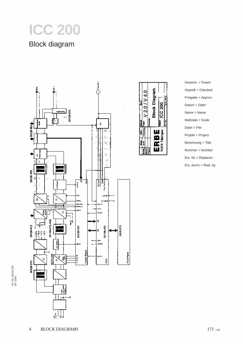
171 / 2664 BLOCK DIAGRAMS
Art
. No.
801
16-2
0109
/ 20
04
ICC 200Block diagram
V 2
.0 /
V 4
.0
Gezeich. = Drawn
Geprüft = Checked
Freigabe = Approv.
Datum = Date*
Name = Name
Maßstab = Scale
Datei = File
Projekt = Project
Benennung = Title
Nummer = Number
Ers. für = Replaces
Ers. durch = Repl. by
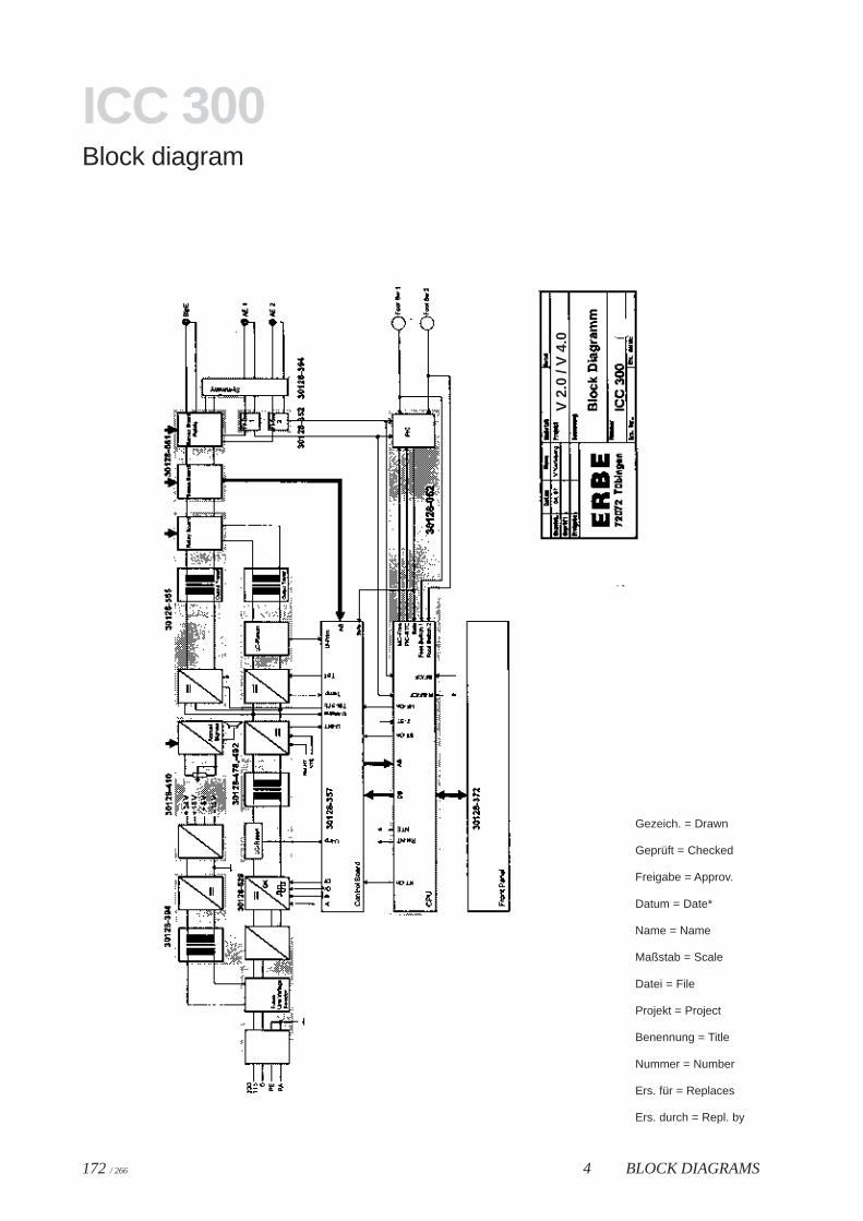
172 / 266 4 BLOCK DIAGRAMS
ICC 300Block diagram
V 2
.0 /
V 4
.0
Gezeich. = Drawn
Geprüft = Checked
Freigabe = Approv.
Datum = Date*
Name = Name
Maßstab = Scale
Datei = File
Projekt = Project
Benennung = Title
Nummer = Number
Ers. für = Replaces
Ers. durch = Repl. by
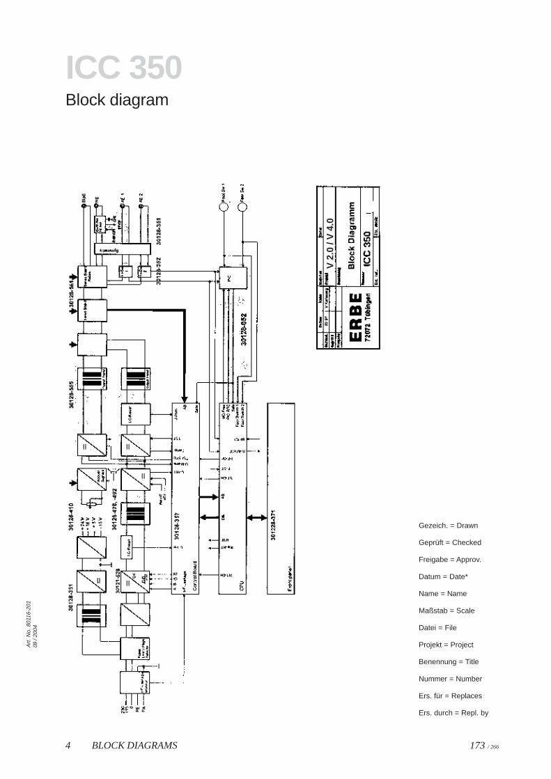
173 / 2664 BLOCK DIAGRAMS
Art
. No.
801
16-2
0109
/ 20
04
ICC 350Block diagram
V 2
.0 /
V 4
.0
Gezeich. = Drawn
Geprüft = Checked
Freigabe = Approv.
Datum = Date*
Name = Name
Maßstab = Scale
Datei = File
Projekt = Project
Benennung = Title
Nummer = Number
Ers. für = Replaces
Ers. durch = Repl. by

Chapter 5Circuit diagrams


PCBs forICC 200, 300, 350
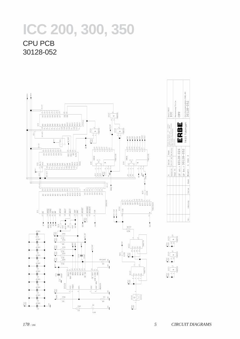
178 / 266 5 CIRCUIT DIAGRAMS
ICC 200, 300, 350CPU PCB30128-052
1
Die
se Z
eic
hn
un
gis
t u
rhe
be
r-
oh
ne
un
sere
Ge
ne
hm
igu
ng
Be
ne
nn
un
g/T
itle
Ze
ich
nu
ng
snu
mm
er/
DW
G.N
O
Ge
rt/U
NIT
We
iterg
ab
e u
nd
Ve
rvie
lfltig
un
gre
chtli
ch g
esc
htz
t,d
ah
er
un
zuls
sig
Da
tum
Na
me
Ge
zeic
h.
Ge
pr
ft
LP
un
.:
LP
bs.
:
Bla
ttvo
nD
atu
mN
am
en
de
run
gN
r.
M.F
ritz
ICC
CP
U
3
30
12
8-0
52
30
12
8-0
52
40
12
8-0
26
29
.07
.92
B
+
BT1
3V
C1
68nF
C10
68nF
C1
1
68
nF
C1
5
10
nF
C2
68nF
C3
68nF
C4
68nF
C5
68nF
C6
68nF
C7
68nF
C8
68nF
C9
68nF
D2
1N4148
30
31
32
33
34
35
36
37
38
39
40 1 2 3 4 5 14
15
12 8 7 9 10
13
A1
0
A1
1
A1
2
A1
3
A1
4
A1
5
A9
A8
A7
A6
A5
A4
A3
A2
A1
A0 D
0
D1
D2
D3
D4
D5
D6
D7
M1
MR
EQ
IOR
Q
RD
WR
RF
SH
HA
LT
WA
IT
INT
NM
I
RE
SE
T
BU
SR
EQ
BU
SA
CK
CL
K
Z8
4C
00
IC1
BA
T O
N
RE
S
PF
D
WD
0
OS
C S
EL
OS
C
VB
AT
VC
C
IC1
0
PF
1
LO
W L
INE
CE
OU
T
CE
IN
WD
1
RE
S
GN
D
MA
X6
91
VN
OT
Q1
Q4
Q5
Q6
Q7
Q8
Q9
Q1
0
Q1
1
Q1
2
Q1
3
Q1
4R
CL
K
IC1
2
74
HC
40
20
GIC
16
SG
53
1P
EN
OU
T
&
74
HC
00
IC1
5&
74
HC
00
IC1
5
N.C
.
VC
C
A1
1
A1
2
A1
0
A9
A8
A7
A6
A5
A4
A3
A2
A1
A0
R/WO
E
CE
1
CE
2
D5
D4
D7
D6
D3
D2
D1
D0
11
12
13
15
16
17
18
19
10
9 8 7 6 5 4 3 25
24
21
IC2
23
2
58
64
&
74
HC
00
IC1
5
&
74
HC
00
IC1
5
&
74
HC
00
IC1
1
&
74
HC
00
IC1
1
74
HC
74
S RIC1
3
C D
74
HC
74
S RIC1
3
C D
CE
OE
D7
D6
D5
D4
D3
D2
D1
D0
19
18
16
17
15
13
12
11
A0
A1
A3
A2
A4
A5
A6
A7
A8
A9
A1
0
A1
1
A1
2
A1
3
10
9 8 7 6 5 4 3 25
24
21
23
2 26
A1
4
A1
5
27
1
27
C5
12
IC3
0 2
G70D
MU
X
74
HC
13
8
0 1 2 3 4 5 6 7
&
IC8
0 2
G70D
MU
X
74
HC
13
8
0 1 2 3 4 5 6 7
&
IC9
JP1
R1
2k2
R10
5k6
R2
1
22
0R
R20
220R
R1
9
22
0R
R11
5k6
R12
5k6
R13
5k6
R1
4
5k6
R3
8k2
R4
1k
R5
5k6
R6
5k6
CE
_IN
CE
_IN
CE
_O
UT
CE
_O
UT
CS
10
CS
11
CS
4
CS
5
CS
6
CS
7
CS
8
CS
9
INT
IOR
Q
IOR
Q
M1
M1
MR
EQ
MR
EQ
RD
RE
S
RE
S
WA
ITWR
WR
AB
US
CL
K
CL
K
DB
US
GN
D
GN
D
GN
DG
ND
GN
DG
ND
GN
D
GN
D
GN
D
J2/7
C
PIC
-CL
K
+2
4V
RE
S
RE
S
SIO
-CL
K
Vcc
+5
VV
cc+
5V
Vcc
+5
V
Vcc
+5
VV
cc+
5V
Vcc
+5
V
Vcc
+5
V
Vcc
+5
VV
cc+
5V
Vcc
+5
V
Vcc
+5
V
Vcc
+5
VV
cc+
5V
Vcc
+5
V
Vcc
+5
V
Vcc
+5
V
VN
OT
VN
OT
VN
OT
WD
I
A1
4
A5
A4
A3
A1
5
A1
4
A1
3
A1
3
16
17
18
19
20
21
22
23
24
25
26
27
28
6
A0
-A1
5
D0
-D7
13
12
15
5 46
7 891
0
16
13
2 14
11
10
9 14
15
1 2 37 5 4 6 13
12
11
15
1 23
4 56
20
22
A0
-A1
5
26
D0
-D7
1
27
28
9 10
81
2
13
11
1 23
4 56
14
6
3 2
5
13
10
8
11
12
9
A0
-A1
5
20
D0
-D7
22
4 51 2 3 6
15
14
13
12
11
10
9 7
4 51 2 3 6
15
14
13
12
11
10
9 7
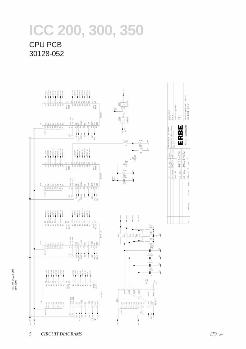
5 CIRCUIT DIAGRAMS 179 / 266
Art
. No.
801
16-2
0109
/ 20
04
ICC 200, 300, 350CPU PCB30128-052
2
Die
se Z
eic
hn
un
gis
t u
rhe
be
r-
oh
ne
un
sere
Ge
ne
hm
igu
ng
Be
ne
nn
un
g/T
itle
Ze
ich
nu
ng
snu
mm
er/
DW
G.N
O
Ge
rt/U
NIT
We
iterg
ab
e u
nd
Ve
rvie
lfltig
un
gre
chtli
ch g
esc
htz
t,d
ah
er
un
zuls
sig
Da
tum
Na
me
Ge
zeic
h.
Ge
pr
ft
LP
un
.:
LP
bs.
:
Bla
ttvo
nD
atu
mN
am
en
de
run
gN
r.
M.F
ritz
ICC
CP
U
3
30
12
8-0
52
30
12
8-0
52
40
12
8-0
26
29
.07
.92
B
C13
+
15uF
C14
+
15uF
C16
180nFC17
180nFC18
180nFC19
1nF
C20
68nF
D1
1N
41
48
D7
D6
D5
D4
D3
D2
D1
D0
A0
A1
RD
RD
Y
CS
AIN
1
AIN
2
AIN
3
AIN
4
VR
EF
+
VR
EF
-
AD
6 7 8 9 17
18
19
20
IC1
4
AD
78
24
&
74
HC
00
IC1
1
&
74
HC
00
IC1
1
20
19
40
39
38
D0
D1
D2
D3
D4
D5
D6
D7
B/A
SE
L
C/D
SE
L
CE
M1
IOR
Q
INT
IEI
IEO
A0
A1
A2
A3
A4
A5
A6
A7
AR
DY
AS
TB B0
B1
B2
B3
B4
B5
B6
B7
BR
DY
BS
TB
1 3 2
RD
CL
K
Z8
0P
IO
IC4
20
19
40
39
38
D0
D1
D2
D3
D4
D5
D6
D7
B/A
SE
L
C/D
SE
L
CE
M1
IOR
Q
INT
IEI
IEO
A0
A1
A2
A3
A4
A5
A6
A7
AR
DY
AS
TB B0
B1
B2
B3
B4
B5
B6
B7
BR
DY
BS
TB
1 3 2
RD
CL
K
Z8
0P
IO
IC5
20
19
40
39
38
D0
D1
D2
D3
D4
D5
D6
D7
B/A
SE
L
C/D
SE
L
CE
M1
IOR
Q
INT
IEI
IEO
A0
A1
A2
A3
A4
A5
A6
A7
AR
DY
AS
TB B0
B1
B2
B3
B4
B5
B6
B7
BR
DY
BS
TB
1 3 2
RD
CL
K
Z8
0P
IO
IC6
20
19
40
39
38
D0
D1
D2
D3
D4
D5
D6
D7
B/A
SE
L
C/D
SE
L
CE
M1
IOR
Q
INT
IEI
IEO
A0
A1
A2
A3
A4
A5
A6
A7
AR
DY
AS
TB B0
B1
B2
B3
B4
B5
B6
B7
BR
DY
BS
TB
1 3 2
RD
CL
K
Z8
0P
IO
IC7
R1
5
1kR
16
1kR
17
1kR
18
1k
R7
680k
R8
5M6
R9
22k
RN1
8*1k
CS
4C
S5
CS
6C
S7
CS
8
INT
INT
INT
INT
IOR
QIO
RQ
IOR
QIO
RQ
M1
RD
RD
RD
RD
RD
RE
S
SIC
HE
R
WA
IT
AB
US
AB
US
CL
KC
LK
CL
KC
LK
DB
US
DB
US
FIS
CH
-A1
FIS
CH
-A2
FIS
CH
-A3
FIS
CH
-B1
FIS
CH
-B2
FIS
CH
-B3
FU
SS
-A1
FU
SS
-A2
FU
SS
-B1
FU
SS
-B2
GN
D
GN
D
GN
DG
ND
GN
D
GN
DG
ND
GN
DG
ND
GN
DG
ND
GN
DG
ND
IEI_
5
IEI_
5IE
I_6
IEI_
6
IEI_
7
IEI_
7
J1/1
0
J1/1
1
J1/1
2
J1/1
3
J1/1
4
J1/1
5
J1/1
6
J1/1
7
J1/1
8
J1/1
9
J1/2
1
J1/2
2
J1/2
4
J1/2
5
J1/2
6
J1/2
7
J1/2
8
J1/2
9
J1/3
0
J1/3
1
J1/3
2
J1/3
3
J1/3
4
J1/3
5
J1/8
J1/9
J2/1
3C
J2/1
8C
J2/1
9C
J2/2
0C
J2/2
3A
J2/2
4A
J2/2
4C
J2/2
5A
J2/2
5C
J2/2
6A
J2/2
6C
J2/2
7A
J2/2
7C
J2/2
8A
J2/2
8C
J2/2
9A
J2/2
9C
J2/3
0A
J2/3
0C
J2/3
1C
J2/6
A
J2/6
C
J2/7
A
J2/7
C
J2/8
A
J2/8
C
J2/9
A
M1
_P
IO
M1
_P
IO
M1
_P
IOM
1_
PIO
M1
_P
IO
MC
-FR
EI
PIC
-RT
CC
Vcc
+5
V
Vcc+5V
Vcc
+5
V
Vcc
+5
V
WD
I
A1
A0
A0
A1
A1
A0
A1
A0
A0
A1
16
10
22
21
4 3 2 1
D0
-D7
15
14
13
9 10
81
2
13
11
10
12
13
14
15
16 17
18 21
22
23
24
25
27
28
29
30
31
32
33
34
35
36
37
456
789
D0
-D7
10
12
13
14
15
16 17
18 21
22
23
24
25
27
28
29
30
31
32
33
34
35
36
37
456
789
D0
-D7
10
12
13
14
15
16 17
18 21
22
23
24
25
27
28
29
30
31
32
33
34
35
36
37
456
789
D0
-D7
10
12
13
14
15
16 17
18 21
22
23
24
25
27
28
29
30
31
32
33
34
35
36
37
456
789
D0
-D7
1
5
4
3
2
9
8
7
6
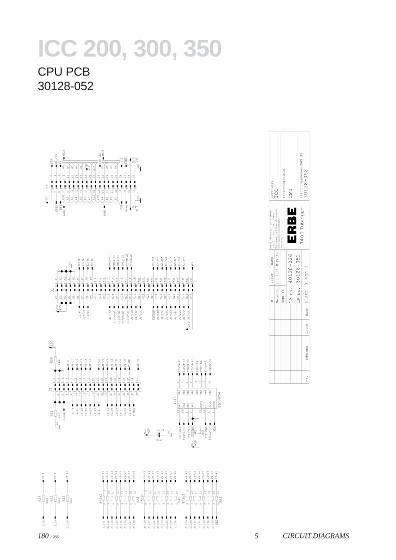
180 / 266 5 CIRCUIT DIAGRAMS
ICC 200, 300, 350CPU PCB30128-052
3
Die
se Z
eic
hn
un
gis
t u
rhe
be
r-
oh
ne
un
sere
Ge
ne
hm
igu
ng
Be
ne
nn
un
g/T
itle
Ze
ich
nu
ng
snu
mm
er/
DW
G.N
O
Ge
rt/U
NIT
We
iterg
ab
e u
nd
Ve
rvie
lfltig
un
gre
chtli
ch g
esc
htz
t,d
ah
er
un
zuls
sig
Da
tum
Na
me
Ge
zeic
h.
Ge
pr
ft
LP
un
.:
LP
bs.
:
Bla
ttvo
nD
atu
mN
am
en
de
run
gN
r.
M.F
ritz
ICC
CP
U
3
30
12
8-0
52
30
12
8-0
52
40
12
8-0
26
29
.07
.92
B
C12
68nF
RA
0
RA
1
RA
2
RA
3
MC
LR
RT
CC
OS
C1
OS
C2
RB
0
RB
1
RB
2
RB
3
RB
4
RB
5
RB
6
RB
7
PIC
16
C5
4
IC1
7
J1J2
J3
R2
6
2k2
R2
5
2k2
R2
4
2k2 R
23
2k2 R
22
2k2
R2
2k2
RA
1
8*2
k2
RA
2
8*2
k2
RA
3
8*2
k2
CS
10
CS
11
CS
9
INT
IOR
QM
RE
Q
RD
RE
S
RE
SR
ES
SIC
HE
R
SIC
HE
R
WR
AB
US
AB
US
DB
US
DB
US
F-G
ND
F-G
ND
F-G
ND
FIS
CH
-A1
FIS
CH
-A1
FIS
CH
-A2
FIS
CH
-A2
FIS
CH
-A3
FIS
CH
-A3
FIS
CH
-B1
FIS
CH
-B1
FIS
CH
-B2
FIS
CH
-B2
FIS
CH
-B3
FIS
CH
-B3
FU
SS
-A1
FU
SS
-A1
FU
SS
-A2
FU
SS
-A2
FU
SS
-B1
FU
SS
-B1
FU
SS
-B2
FU
SS
-B2
GN
D
GN
D
GN
D
GN
DG
ND
J1-1
0
J1-1
0
J1-1
1
J1-1
1
J1-1
2
J1-1
2
J1-1
3
J1-1
3
J1-1
4
J1-1
4
J1-1
5
J1-1
5
J1-1
6
J1-1
6
J1-1
7
J1-1
7
J1-1
8
J1-1
8
J1-1
9
J1-1
9
J1-2
1
J1-2
1
J1-2
2
J1-2
2
J1-2
4
J1-2
4
J1-2
5
J1-2
5
J1-2
6
J1-2
6
J1-2
7
J1-2
7
J1-2
8
J1-2
8
J1-2
9
J1-2
9
J1-3
0
J1-3
0
J1-3
1
J1-3
1
J1-3
2
J1-3
2
J1-3
3
J1-3
3
J1-3
4
J1-3
4
J1-3
5
J1-3
5
J1-4
0
J1-4
0
J1-8
J1-8
J1-9
J1-9
J1/1
0
J1/1
1
J1/1
2
J1/1
3
J1/1
4
J1/1
5
J1/1
6
J1/1
7
J1/1
8
J1/1
9
J1/2
1
J1/2
2
J1/2
4
J1/2
5
J1/2
6
J1/2
7
J1/2
8
J1/2
9
J1/3
0
J1/3
1
J1/3
2
J1/3
3
J1/3
4
J1/3
5
J1/8
J1/9
J2/1
3C
J2/1
8C
J2/1
9C
J2/2
0C
J2/2
3A
J2/2
4A
J2/2
4C
J2/2
5A
J2/2
5C
J2/2
6A
J2/2
6C
J2/2
7A
J2/2
7C
J2/2
8A
J2/2
8C
J2/2
9A
J2/2
9C
J2/3
0A
J2/3
0C
J2/3
1C
J2/6
AJ2
/6C
J2/7
AJ2
/7C
J2/8
AJ2
/8C
J2/9
A
M1
_P
IO
MC
-FR
EI
PIC
-CL
K
PIC
-RT
CC
+2
4V
RE
S
SIO
-CL
K
Vcc
+5
V
Vcc
+5
V
Vcc
+5
V
Vcc
+5
V
Vcc+5V
Vcc+5V
VN
OT
D0
D2
D5
D4
A1
5
A1
3
A1
1
A0
A2
A4
A6
A8
A1
0
D1
D7
D6
D3
A1
4
A1
2
A1
A3
A5
A7
A9
416
15
17
18
1 2
6 7 8 9 10
11
12
13
3
1
10
11
12
13
14
15
16
17
18
19
2
20
21
22
23
24
25
26
27
28
29
3
30
31
32
33
34
35
36
37
38
39
4
40
56
78
9
A1
A1
0
A1
1
A1
2
A1
3
A1
4
A1
5
A1
6
A1
7
A1
8
A1
9
A2
A2
0
A2
1
A2
2
A2
3
A2
4
A2
5
A2
6
A2
7
A2
8
A2
9
A3
A3
0
A3
1
A3
2
A4
A5
A6
A7
A8
A9
C1
C1
0
C1
1
C1
2
C1
3
C1
4
C1
5
C1
6
C1
7
C1
8
C1
9
C2
C2
0
C2
1
C2
2
C2
3
C2
4
C2
5
C2
6
C2
7
C2
8
C2
9
C3
C3
0
C3
1
C3
2
C4
C5
C6
C7
C8
C9
1
10
11
12
13
14
15
16
17
18
19
2
20
21
22
23
24
25
26
27
28
29
3
30
31
32
33
34
35
36
37
38
39
4
40
56
78
9
1
10
11
12
13
14
15
16
23456789
1
10
11
12
13
14
15
16
23456789
1
10
11
12
13
14
15
16
23456789
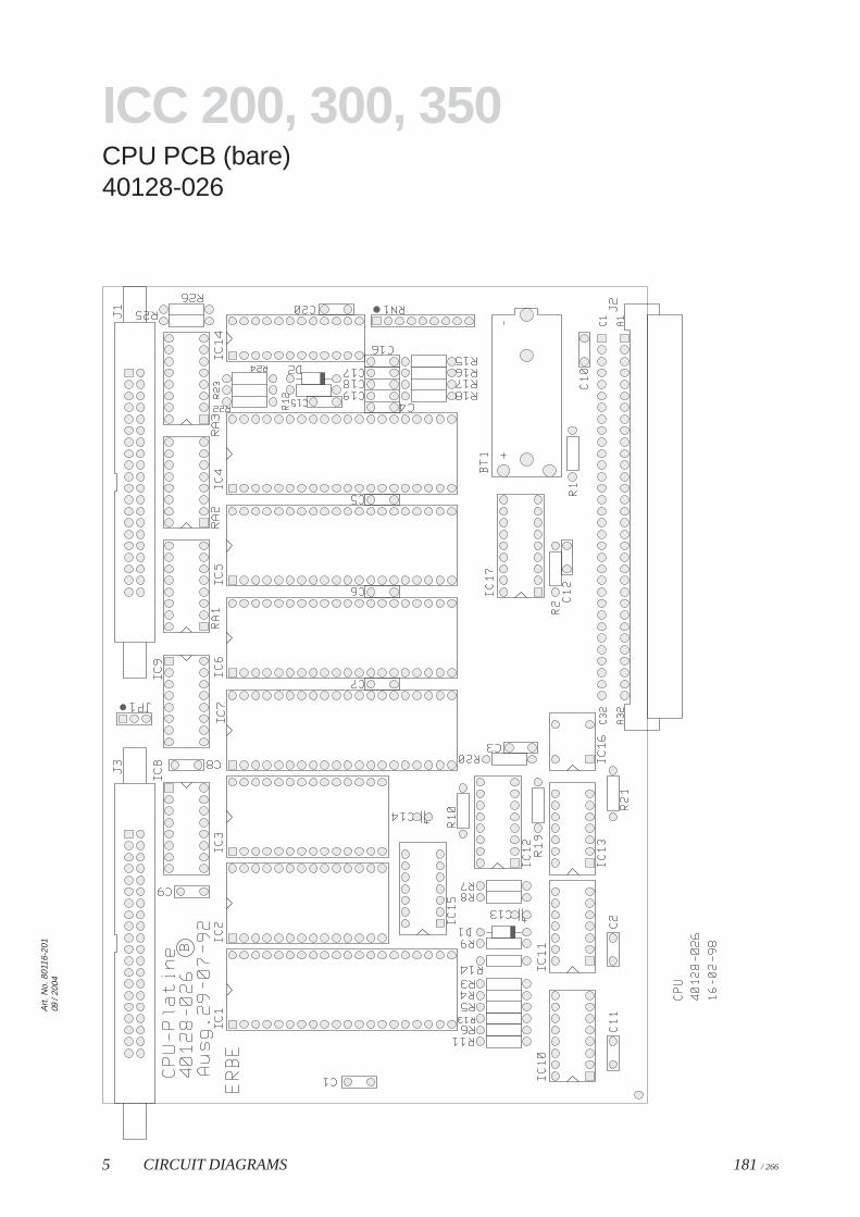
5 CIRCUIT DIAGRAMS 181 / 266
Art
. No.
801
16-2
0109
/ 20
04
ICC 200, 300, 350CPU PCB (bare)40128-026
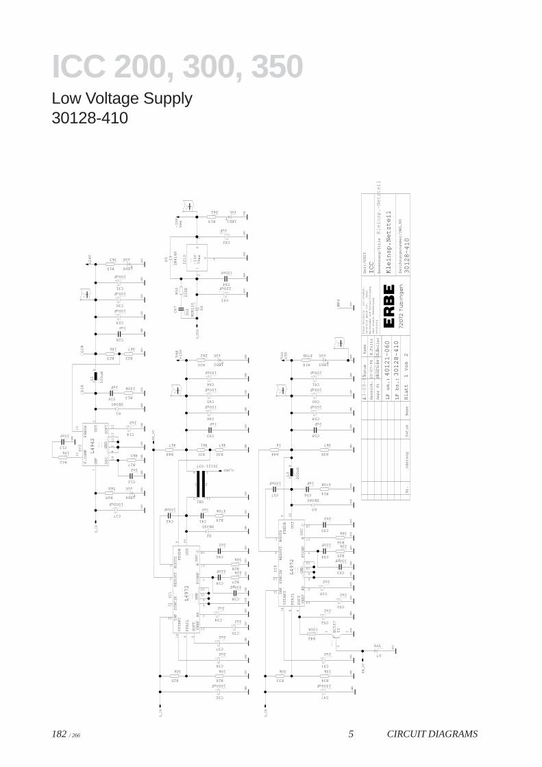
182 / 266 5 CIRCUIT DIAGRAMS
ICC 200, 300, 350Low Voltage Supply30128-410
1
Die
se Z
eic
hn
un
gis
t u
rhe
be
r-
oh
ne
un
sere
Ge
ne
hm
igu
ng
Be
ne
nn
un
g/T
itle
Ze
ich
nu
ng
snu
mm
er/
DW
G.N
O
Ge
rt/U
NIT
We
iterg
ab
e u
nd
Ve
rvie
lfltig
un
gre
chtli
ch g
esc
htz
t,d
ah
er
un
zuls
sig
Da
tum
Na
me
Ge
zeic
h.
Ge
pr
ft
LP
un
.:
LP
bs.
:
Bla
ttvo
nD
atu
mN
am
en
de
run
gN
r.
ICC
Kle
insp
.Ne
tzte
il4
01
21
-06
0
M.F
ritz
23
01
28
-41
0
30
12
8-4
10
A
20
-07
-94
20
-07
-94
J.B
elle
r1.0
0.7
0.7
0.7
0.7
C12
2n2
C13
22nF C14
+
2u2
C26
1nF
C28
1uF
C29
+
100uF
C30
+
100uF
C31
+
100uF
C17
+
1000uF
C56
1nF
C58
1uF
C59
+
100uF
C60
+
100uF
C61
+
100uF
C55
2n2
C54
22nF
C53
330pF
C57
100nF
C49
+
2u2
C50
+
2u2
C52
+
2u2
C51
+
2u2
C41
1nF
C43
1uF
C46
+
100uF
C45
+
100uF
C44
+
100uF
C40
2n2
C39
22nF
C38
330pF
C42
100nF
C34
+
2u2
C35
+
2u2
C37
+
2u2
C36
+
2u2
C6
7
2n
2
C64
100nF
C63
+
220uF
C62
+
1uF
C47
+
1000uF
C32
+
1000uF
D1
SB340
D5
1N
41
48
LED6
rot
D3
SB340
LED3
rot
D2
SB340
LED2
rot
D6
MU
R1
20
LED1
rot
D7
5V6
LED4
rot
INP
OU
T
IC3
L4
96
2
GN
DS
OF
TO
SC
F.C
OM
PF
EE
DB
GN
D
IC6
L4
97
2RE
SO
UT
SY
NC
ININ
PB
OO
TS
FE
ED
B
OU
TP
FA
IL
VS
TA
RT
VR
EF
SO
FT
RD
FC
OM
PR
CO
SC
GN
D
IC1
L4
97
2RE
SO
UT
SY
NC
ININ
PB
OO
TS
FE
ED
B
OU
TP
FA
IL
VS
TA
RT
VR
EF
SO
FT
RD
FC
OM
PR
CO
SC
IO
G
IC1
0
79
xx-1
5V
L3
20
0u
H
L1
10
0u
H
L1
B
MP
4
L1
A
R17
4k3
R12
15k
R13
100R
R23
18k
R22
4k7
R15
3k3
R14
470R
R38
4k7
R18
470R
R36
36k
R35
22k
R42
100R
R44
1k
R33
30k
R34
10k
R29
470R
R31
9k1
R30
4k7
R20
2k2
R28
36k
R27
22k
R48
4k7
R25
30k
R26
10k
R5
0
22
0R
R19
2k2
R49
5k6
T2
BC
55
7
UE1
30121-037
1 2
EN
_5
V
EN
_5
V
GN
D
GN
DG
ND
GN
D
GN
DG
ND
GN
DG
ND
GN
DG
ND
GN
DG
ND
GN
D
GN
D
GN
DG
ND
GN
D
GN
D
GN
D
GN
DG
ND
GN
DG
ND
GN
DG
ND
GN
DG
ND
GN
DG
ND
GN
DG
ND
GN
DG
ND
GN
DG
ND
GN
DG
ND
GN
D
GN
DG
ND
GN
DG
ND
GN
DG
ND
GN
DG
ND
GN
DG
ND
GN
DG
ND
GN
DG
ND
GN
DG
ND
GN
DG
ND
GN
DG
ND
GN
DG
ND
GN
DG
ND
+2
4V
U_
IN
U_
IN
U_
IN
U_NEG
U_
NE
G
Vcc
+5
V
+1
5V
Vd
dV
ee
-15
V
11
10
45
12
13
7
14
2
15
1
18
9
7
5
6
15
16
11
20
4
17
2
3
8
10
13
14
1
18
9
7
5
6
15
16
11
20
4
17
2
3
8
10
13
14
1
23
58
58
2
31
5
8
11
2
Kle
insp
.-N
etz
teil
40
12
1-0
60
13
-09
-95
$plname
$plname
ec50r25
$plname
c100
ec130r50
ec130r50
ec130r50
ec380_17
$plname
c100
ec130r50
ec130r50
ec130r50
$plname
$plname
$plname
$plname
ec50r25
ec50r25
ec50r25
ec50r25
$plname
c100
ec130r50
ec130r50
ec130r50
$plname
$plname
$plname
$plname
ec50r25
ec50r25
ec50r25
ec50r25
$p
lna
me
$plname
ec130r50
$plname
ec380_17ec380_17
$plname
$p
lna
me$plname
$plname
$plname
$plname
$plname
$p
lna
me
$plname
$plname
$plname
$rp
na
me
$p
lna
me
$rp
na
me
$p
lna
me
$rp
na
me
$p
lna
me
to2
20
l
$p
lna
me
$p
lna
me
$plname
$plname
$plname
$plname $plname
$plname
$plname
$plname
$plname
$plname
$plname
$plname
$plname
$plname $plname
$plname
$plname $plname
$plname
$plname
$plname
$plname
$plname $plname
$p
lna
me
$plname
$plname
$p
lna
me
$plname
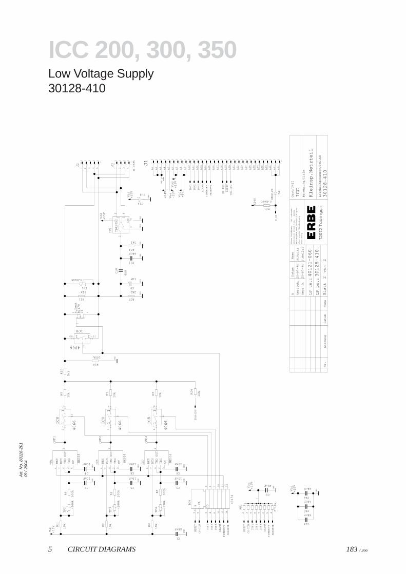
5 CIRCUIT DIAGRAMS 183 / 266
Art
. No.
801
16-2
0109
/ 20
04
ICC 200, 300, 350Low Voltage Supply30128-410
n.b
est
n.b
est
2
Die
se Z
eic
hn
un
gis
t u
rhe
be
r-
oh
ne
un
sere
Ge
ne
hm
igu
ng
Be
ne
nn
un
g/T
itle
Ze
ich
nu
ng
snu
mm
er/
DW
G.N
O
Ge
rt/U
NIT
We
iterg
ab
e u
nd
Ve
rvie
lfltig
un
gre
chtli
ch g
esc
htz
t,d
ah
er
un
zuls
sig
Da
tum
Na
me
Ge
zeic
h.
Ge
pr
ft
LP
un
.:
LP
bs.
:
Bla
ttvo
nD
atu
mN
am
en
de
run
gN
r.
ICC
Kle
insp
.Ne
tzte
il4
01
21
-06
0
M.F
ritz
23
01
28
-41
0
30
12
8-4
10
A
20
-07
-94
20
-07
-94
J.B
elle
r
C1
68nF
C1
0
6n
8
C11
68nF
C16
+
3u3
C18
68nF
C2
68nFC3
10nF
C4
10nF
C5
10nF
C6
10nF
C65
68nF
C66
68nFC7
10nF
C8
10nF
C9
+
1uF
D4
MU
R1
20
IC8
1
40
66
1
IC8
1
40
66
1
IC8
1
40
66
1
IC2
TD
A7
05
2
GN
D
+
IC8
1
4066
1
CV
TR
G
TH
D
DC
H
RE
S
IC4
OU
T
NE
55
5
CV
TR
G
TH
D
DC
H
RE
S
IC5
OU
T
NE
55
5
CV
TR
G
TH
D
DC
H
RE
S
IC7
OU
T
NE
55
5
1DR C
1 40
17
4
IC9
J1J2 J3
MP
1
MP
2
MP
3
R1
10
kR
10
5k1
R11
51k
R16
100k
R2
10
k
R21
n.best
R2
4
10
k
R3
10
k
R37
2k2
R39
5k1
R4
10
0k
R5
10
k
R6
10
0k
R7
10
k
R8
10
0k
R9
10
k
RN
1
8*1
0k
T1
BS
17
0
TP1
n.best
TP
2 20
0k
TP
3 20
0k
TP
4 20
0k
RE
SE
T
RE
SE
T
RE
SE
T
AL
AR
M
AL
AR
M
AL
AR
M
CS
-TO
N
CS
-TO
N
CS
-TO
N
GN
D
GN
D
GN
D
GN
DG
ND
GN
DG
ND
GN
DG
ND
GN
D
GN
DG
ND
GN
DG
ND
GN
D
GN
D
GN
D
GN
D
+2
4V
+2
4V
RE
SE
RV
E
RE
SE
RV
E
RE
SE
RV
E
TIM
ER
OF
F
TIM
ER
OF
F
TIM
ER
OF
F
TO
N-C
PU
TO
N-C
PU
TO
N1
TO
N1
TO
N1
TO
N2
TO
N2
TO
N2
TO
N3
TO
N3
TO
N3
U_
IN
Vcc
+5
V
+1
5V
Vd
d
+1
5V
Vd
d
+1
5V
Vd
d
+1
5V
Vd
d
+1
5V
Vd
d
+1
5V
Vd
d
Ve
e-1
5V
21
13
34
5
98
6
6
2
5 8
3
1
10 11
12
57
3
4 6 2 57
3
4 6 2 57
3
4 6 2
1 32
45
67
11
10
13
12
14
15
9
A1
A1
0
A1
1
A1
2
A1
3
A1
4
A1
5
A1
6
A1
7
A1
8
A1
9
A2
A2
0
A2
1
A2
2
A2
3
A2
4
A2
5
A2
6
A2
7
A2
8
A2
9
A3
A3
0
A3
1
A3
2
A4
A5
A6
A7
A8
A91 2 3 4 5 1 2 3 4
1
2 3 9 8 7 6 5 4
3
2
1
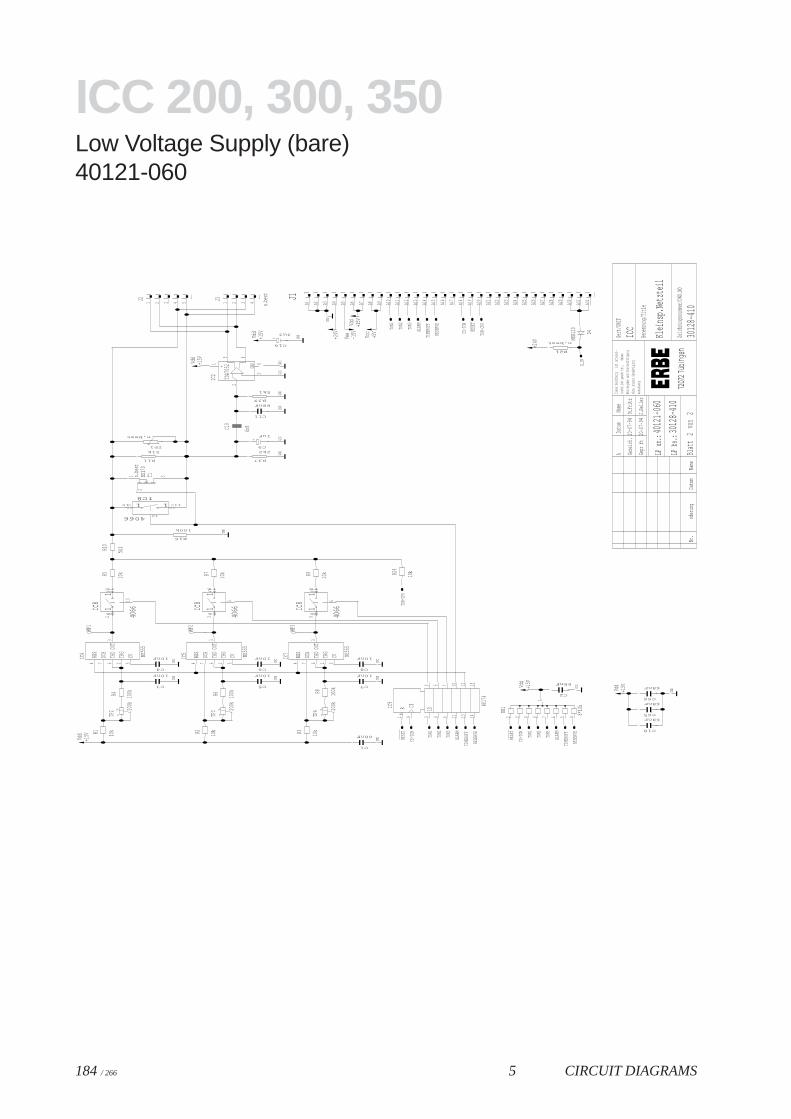
184 / 266 5 CIRCUIT DIAGRAMS
ICC 200, 300, 350Low Voltage Supply (bare)40121-060
n.bes
t
n.bes
t
2
Diese
Zeich
nung
ist ur
hebe
r-
ohne
unse
re Ge
nehm
igung
Bene
nnun
g/Title
Zeich
nung
snum
mer/D
WG.N
O
Gert/U
NIT
Weite
rgabe
und V
erviel
fltigu
ngrec
htlich
gesc
htzt
,da
her
unzu
lssig
Datum
Name
Geze
ich.
Gepr
ft
LP un
.:
LP bs
.:
Blatt
von
Datum
Name
nderu
ngNr
.
ICC
Kleins
p.Netz
teil
4012
1-060M.Fri
tz
230
128-4
10
3012
8-410
A
20-07
-94
20-07
-94J.B
eller
C1
68nF
C10
6n8
C11
68nF
C16
+
3u3
C18
68nF
C2
68nFC3
10nF
C4
10nF
C5
10nF
C6
10nF
C65
68nF
C66
68nFC7
10nF
C8
10nF
C9
+
1uF
D4
MUR1
20
IC8
1
4066
1
IC8
1
4066
1
IC8
1
4066
1
IC2 TD
A705
2 GND
+
IC8
1
4066
1
CVTRG
THD
DCH
RES
IC4
OUT
NE55
5
CVTRG
THD
DCH
RES
IC5
OUT
NE55
5
CVTRG
THD
DCH
RES
IC7
OUT
NE55
5
1DR C1 4017
4
IC9
J1J2 J3
MP1
MP2
MP3
R1 10k
R10
5k1
R11
51k
R16
100k
R2 10k
R21
n.best
R24
10k
R3 10k
R37
2k2
R39
5k1
R4 100k
R5 10k
R6 100k
R7 10k
R8 100k
R9 10k
RN1
8*10k
T1BS17
0
TP1
n.best
TP2 20
0k
TP3 20
0k
TP4 20
0k
RESE
T
RESE
T
RESE
T
ALAR
M
ALAR
M
ALAR
M
CS-TO
N
CS-TO
N
CS-TO
N
GND
GND
GND
GND
GND
GND
GND
GND
GND
GND
GND
GND
GND
GND
GND
GND
GND
GND
+24V
+24V
RESE
RVE
RESE
RVE
RESE
RVE
TIMER
OFF
TIMER
OFF
TIMER
OFF
TON-
CPU
TON-
CPU
TON1
TON1
TON1
TON2
TON2
TON2
TON3
TON3
TON3
U_IN
Vcc
+5V
+15VVdd
+15VVdd
+15VVdd
+15VVdd
+15VVdd
+15VVdd
Vee
-15V
21
13
34
5
98
6
6
2
5 8
3
1
10 11
12
57
3
4 6 2 57
3
4 6 2 57
3
4 6 2
1 32
45
67
1110
1312
1415
9
A1 A10
A11
A12
A13
A14
A15
A16
A17
A18
A19
A2 A20
A21
A22
A23
A24
A25
A26
A27
A28
A29
A3 A30
A31
A32
A4 A5 A6 A7 A8 A91 2 3 4 5 1 2 3 4
1
2 3 9 8 7 6 5 4
3
2
1
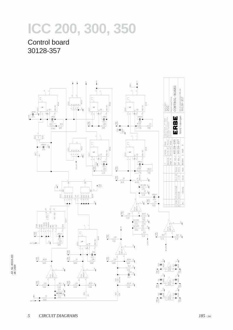
5 CIRCUIT DIAGRAMS 185 / 266
Art
. No.
801
16-2
0109
/ 20
04
ICC 200, 300, 350Control board30128-357
1
Die
se Z
eic
hn
un
gis
t u
rhe
be
r-
oh
ne
un
sere
Ge
ne
hm
igu
ng
Be
ne
nn
un
g/T
itle
Ze
ich
nu
ng
snu
mm
er/
DW
G.N
O
Ge
rt/U
NIT
We
iterg
ab
e u
nd
Ve
rvie
lfltig
un
gre
chtli
ch g
esc
htz
t,d
ah
er
un
zuls
sig
Da
tum
Na
me
Ge
zeic
h.
Ge
pr
ft
LP
un
.:
LP
bs.
:
Bla
ttvo
nD
atu
mN
am
en
de
run
g3
CO
NT
RO
L-B
OA
RD
ICC
15
.02
.94
Fritz
40
12
8-0
95
30
12
8-3
57
Ha
gg
28
-11
-94
33
71
Nr.
Fritz
11
-94
B
30
12
8-3
57
C
C
R1
2=
10
R
Fritz
35
84
C3
7,C
38
=3
30
pF
30
-1-9
6
C9
68
nF
C8
68
nF
C28
100pF
C16
2n2
C15
100pF
C21
33pF
C31
33pF
C32
33pFC20
68nF
C10
2n2
C1
2
68
nF
C1
1
68
nF
C22
100pF
C29
100pF
C19
220pF
C3
0
68
nF
C1
8
68
nF
C1
7
68
nF
D11
1N4148
D12
1N4148
D1
0
1N
41
48
D17
1N4148
D16
1N4148
D15
1N4148
D13
3V6
D14
3V6
40
47
RC
X
CX
Q Q
IC1
8
AS
T
-TR
IG
+T
RIG
RT
RIG
MR
RX
AS
T
OS
C O
UT
G
IA3
IA2
IA1
IA0 S1
S0
IB3
IB2
IB1
IB0
EB
EA
OA
OB
IC1
1
45
39
IC1
3
CX
R
&
RX
/CX 4
52
8
IC9
+- LM
31
9G
ND
IC9
+- LM
31
9G
ND
-+
IC4
LM
31
9
IC1
2
40
30
=1
IC1
3
CX
R
&
RX
/CX 4
52
8
S RIC2
1
40
13
C D
S RIC2
1
40
13
C D
IC1
7
CX
R
&
RX
/CX 4
52
8
IC1
7
CX
R
&
RX
/CX 4
52
8
IC4
+- LM
31
9G
ND
-+
IC9
LM
31
9
IC1
4
+- LM
31
9G
ND
IC1
6
CX
R
&
RX
/CX 4
52
8
IC1
6
CX
R
&
RX
/CX 4
52
8
IC1
4
+- LM
31
9G
ND
-+
IC1
4L
M3
19
MP
1
MP
2
R52
1k
R51
7k5
R53
10R
R58
560R
R5
6
1k
R59
4k7
R60
180R
R69
1k
R88
8k2
R68
9k1
R65
43k
R77
5k6
R86
5k6
R5
7
10
k
R61
820R
R50
10k
R48
560R
R49
2k2
R54
4k7
R80
1k
R81
470R
R73
1k
R78
1k
R72
33k
R70
4k7
R71
100R
R76
1k
R74
10k
R75
10k
R6
7
1k
BS
17
0
T4
TP13
20k
TP15
5k
TP14
5k
HF
_E
IN
A AN
AU
S
BE
IN_
AU
S GN
D
GN
D
GN
DG
ND
GN
D
GN
D
GN
DG
ND
GN
D
GN
D
GN
DG
ND
GN
D
GN
DG
ND
GN
DG
ND
GN
DG
ND
GN
DG
ND
GN
DG
ND
GN
D
GN
DG
ND
GN
D
GN
D
GN
D
GN
DG
ND
GN
DG
ND
GN
D
GN
D
IPB
NT_EIN
TS
I
U_INP
U_
PR
IM
+1
5V
Vd
d
+1
5V
+1
5V
Vd
d+
15
VV
dd
+1
5V
Vd
d+
15
VV
dd
+1
5V
Vd
d
+1
5V
Vd
d
+1
5V
Vd
d+
15
VV
dd
+1
5V
Vd
d
+1
5V
Vd
d
+1
5V
Vd
d
+1
5V
Vd
d+
15
VV
dd
+15VVdd
+1
5V
Vd
d
+1
5V
Vd
d
+1
5V
Vd
d+
15
VV
dd
+1
5V
Vd
d
Ve
e-1
5V
Ve
e-1
5V
Ve
e-1
5V
864
11
5 19
13
10
312
2
1 15
6 5 4 3 10
11
12
13
7 9
14
2
3
7
5 4 1
6
2
5
34
12
10
89
7
611
1 23
13
9
11
12
15
10
14
2
3 4561
12
11
10
981
3
3
7
5 4 1
6
2
13
9
11
12
15
10
14
10
89
7
611
5
34
12
3
7
5 4 1
6
2
13
9
11
12
15
10
14
10
89
7
611
3
2
1
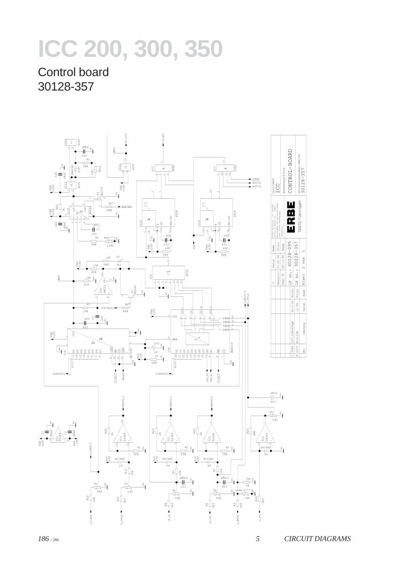
186 / 266 5 CIRCUIT DIAGRAMS
ICC 200, 300, 350Control board30128-357
2
Die
se Z
eic
hn
un
gis
t u
rhe
be
r-
oh
ne
un
sere
Ge
ne
hm
igu
ng
Be
ne
nn
un
g/T
itle
Ze
ich
nu
ng
snu
mm
er/
DW
G.N
O
Ge
rt/U
NIT
We
iterg
ab
e u
nd
Ve
rvie
lfltig
un
gre
chtli
ch g
esc
htz
t,d
ah
er
un
zuls
sig
Da
tum
Na
me
Ge
zeic
h.
Ge
pr
ft
LP
un
.:
LP
bs.
:
Bla
ttvo
nD
atu
mN
am
en
de
run
g3
CO
NT
RO
L-B
OA
RD
ICC
15
.02
.94
Fritz
40
12
8-0
95
30
12
8-3
57
Ha
gg
28
-11
-94
33
71
Nr.
Fritz
11
-94
B
30
12
8-3
57
C
C
R1
2=
10
R
Fritz
35
84
C3
7,C
38
=3
30
pF
30
-1-9
6
C6
+
3u3
C7
2n
2
C13
2n2
C14
2n2
C2
6
68
nF
C23
33pF
C27
1nF
C24
1nF
C2
5
68
nF
C3
68
nF
C1
68
nF
C36
+
15uF
C38
330pF
C37
330pF
rot
D1
D9
1N4148
D1
8
1N
41
48
D5
1N4148
D6
1N4148
D7
1N4148
D7
D6
D5
D4
D3
D2
D1
D0
A0
A1
WR
C0
C1
C2
C3
DA
ANA3
ANA2
ANA1
ANA0
REFC
S
VCC
MA
X5
16
IC6
18
17
16
15
14
13
12
11
1
IC5 4
07
8
IC1
0
CX
R
&
RX
/CX 4
52
84
08
2
&
IC7
40
82
&
IC7
D7
D6
D5
D4
D3
D2
D1
D0
WR
IC8
13
12
11
10 9 8 7 6
VO
UT
AD
72
24
RE
S
CS
LD
AC
D
AIC
4
+- LM
31
9G
ND
IC1
0
CX
R
&
RX
/CX 4
52
8
IC1
+- TL
08
4
IC1
+- TL
08
4
IC1
+- TL
08
4
IC2
+- LM
32
4
DG
ND
Fo
ut
RT
CT
CT
Vin
U F
+ -
IC1
5
AD
65
4
IC1
2
40
30
=1
IC1
2
40
30
=1
IC1
2
40
30
=1
-+
IC1
TL
08
4M
P5
MP
3
R55
1k
R47
1k
R38
4k7 R43
4k7R62
4k7
R66
3k9
R2
3
2k R
22
2k
R24
2k
R21
2k
R5
10
k R7
10
k
R4
3k3 R
6
3k3 R
3
5k6
R2
6
3k3R
12
10
R
R3
6
2k
R35
2k
R1
0
10
k
R1
1
3k3
R44
10k
R2
5
68
k
R8
3
1k R85
10k
R84
2k
R82
1k
R79
4k7
R1
5k1
T1
BC
54
7
BS
17
0
T5
TP4
5k
TP1
n.best
TP2
5k
TP3
5kTP8
5k
TP7
5k
TP17
20k
TP
16
10
k
CS
_D
AC
1
CS
_D
AC
2
RE
SE
T
RESET
STE_EIN
AN
AL
OG
_1
AN
AL
OG
_2
AN
AL
OG
_3
DA
C_
A0
DA
C_
A1
EIN
_A
US
FUNKE_AUS
GN
D
GN
D
GN
D
GN
D
GN
DG
ND
GN
D
GN
DG
ND
GN
D
GN
DG
ND
GN
D
GN
D
GN
D
GN
D
GN
D
GN
D
GN
D
GN
D
GN
D
GN
D
GN
D
GN
D
GN
D
GN
D
GN
D
GN
D
GN
D
GN
D
GN
D
GN
D
GN
D
GN
D
GN
D
IP_
PA
T
IPB
NT_EIN
SICHER
STEUERBUS STEUERBUS
TS
I_S
TE
U_
FU
NK
EU
_F
UN
KE
/2
U_
INT
U_
INT
_A
U_
NE
TZ
T
U_
NE
TZ
T/2
U_
PH
AS
E
UP
_H
F
Vcc
+5
V
Vcc
+5
V
Vcc
+5
V
Vcc
+5
V
+1
5V
Vd
d
+1
5V
Vd
d
+1
5V
Vd
d
+1
5V
Vd
d
+1
5V
Vd
d
+1
5V
Vd
d
+1
5V
Vd
d
+1
5V
Vd
d
+1
5V
Vd
d
Ve
e-1
5V
7810
9
D0
-D7
54
21
20
2 1 24
23
31
9
2 3 4 5 9 10
11
12
13
3
7
5 4 1
6
2
2 3 4 5
1
9 10
11
12
13
14
16
17
15
4
D0
-D7
51
8
2
31
5
34
12
13
9
11
12
15
10
14
6 5
7
2 3
1
13
12
14
2 3
1
7 621
58
34
6 54
8 9
13
12
11
114
2
3 1
3
2
1
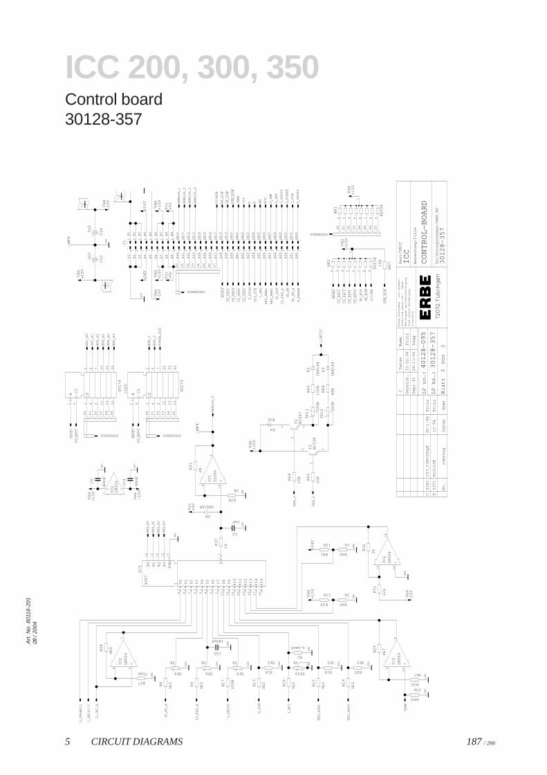
5 CIRCUIT DIAGRAMS 187 / 266
Art
. No.
801
16-2
0109
/ 20
04
ICC 200, 300, 350Control board30128-357
3
Die
se Z
eic
hn
un
gis
t u
rhe
be
r-
oh
ne
un
sere
Ge
ne
hm
igu
ng
Be
ne
nn
un
g/T
itle
Ze
ich
nu
ng
snu
mm
er/
DW
G.N
O
Ge
rt/U
NIT
We
iterg
ab
e u
nd
Ve
rvie
lfltig
un
gre
chtli
ch g
esc
htz
t,d
ah
er
un
zuls
sig
Da
tum
Na
me
Ge
zeic
h.
Ge
pr
ft
LP
un
.:
LP
bs.
:
Bla
ttvo
nD
atu
mN
am
en
de
run
g3
CO
NT
RO
L-B
OA
RD
ICC
15
.02
.94
Fritz
40
12
8-0
95
30
12
8-3
57
Ha
gg
28
-11
-94
33
71
Nr.
Fritz
11
-94
B
30
12
8-3
57
C
C
R1
2=
10
R
Fritz
35
84
C3
7,C
38
=3
30
pF
30
-1-9
6
0.6
0.6
0.8
C2
1nF
C3
3
+
3u
3
C3
4
+
3u
3C
5
68
nF
C4
68
nF
C35
180nF
D2
1N
41
48
D3
1N
41
48
D4
8V2
D8
1N4148
Z
Y1
0
Y1
1
Y1
2
Y1
3
Y1
4
Y1
5
Y9
Y8
Y7
Y6
Y5
Y4
Y3
Y2
Y1
Y0
A1
A2
A3
INH
IC3 A
04
06
7
IC2
+- LM
32
4
IC2
+- LM
32
4
IC1
+- TL
08
4
1DR C
1 40
17
4IC
2
+- LM
32
4
1DR C
1 40
17
4
IC2
0-+
IC2
LM
32
4
J1
MP
4
MP
6
R8
3k3 R
9
3k3 R
17
10
0R
R1
3
3k3
R14
5k1
R1
8
3k3
R2
n.best
R1
5
3k3
R16
3k3
R1
9
3k3
R20
3k3
R2
9
4k7
R30
4k7
R39
10k
R40
2k
R41
10k
R42
2k
R3
1
12
k
R3
2
2k
R3
7
1k
R3
3
2k
R34
2k
R2
8
6k8
R27
750R
R8
7
10
k
R6
4
10
k
R4
6
68
RR4
5
10
0R
R6
3
10
k
R89
10k
RN
1
8x1
0k
RN
2
8x1
0k
T3
BC
33
8
T2
BC
54
7
TP5
5k
TP6
5k
TP9
5k
TP10
5k
TP
11 50
0R
TP
12 50
0R
CS
_D
AC
1
CS
_D
AC
1
CS
_D
AC
2
CS
_D
AC
2
CS
_D
FF
1
CS
_D
FF
1
CS
_D
FF
1
CS
_D
FF
2
CS
_D
FF
2
CS
_D
FF
2
HF
_E
IN
HF
_E
IN
RE
SE
T
RE
SE
T
RE
SE
T
RE
SE
T
ST
E_
EIN
ST
E_
EIN
A AN
AN
AL
OG
_1
AN
AL
OG
_2
AN
AL
OG
_3
AN
AL
OG
_4
AN
AL
OG
_4
AU
S
B
BE
R_
1
BE
R_
1
BE
R_
2
BE
R_
2
DA
C_
A0
DA
C_
A1
FU
NK
E_
AU
S
GN
D
GN
D
GN
D
GN
D
GN
D
GN
D
GN
D
GN
DG
ND
GN
D
GN
D
GN
D
GN
D
GN
DG
ND
GN
D
GN
D
GN
DG
ND
GN
D
GN
D
GN
D
I_H
FL
I_H
FL
IP_
PA
T
IP_
PA
T_
A
IP_
PA
T_
A
MU
X_
A0
MU
X_
A0
MU
X_
A1
MU
X_
A1
MU
X_
A2
MU
X_
A2
MU
X_
A3
MU
X_
A3
NT
_E
IN
NT
_E
IN
+2
4V
+2
4V
+2
4V
RE
S_
AN
A1
RE
S_
AN
A1
RE
S_
AN
A2
RE
S_
AN
A2
SIC
HE
R
SIC
HE
RSTEUERBUS
STEUERBUS
STEUERBUSSTEUERBUS
TE
MP
TE
MP
TS
I
TS
I_S
TE
U_
FU
NK
E
U_
FU
NK
E/2
U_
INP
U_
INT
U_
INT
_A
U_
NE
SS
Y
U_
NE
SS
Y
U_
NE
TZ
T
U_
NE
TZ
T
U_
NE
TZ
T/2
U_
PH
AS
E
U_
PR
IM
U_
SY
M
U_
SY
M
UP
_H
F
UP
_H
F_
A
UP
_H
F_
AV
cc+
5V
Vcc
+5
V
Vcc
+5
V
+1
5V
Vd
d
+1
5V
Vd
d
+1
5V
Vd
d
+1
5V
Vd
d
+1
5V
Vd
d
+1
5V
Vd
d
+1
5V
Vd
d
+1
5V
Vd
dV
ee
-15
V
Ve
e-1
5V
Ve
e-1
5V
Ve
e-1
5V
D7
D5
D4
D6
D3
D2
D1
D0
D5
D4
D3
D2
D1
D0
D5
D4
D3
D2
D1
D0
D7
D6
D5
D4
D3
D2
D1
D0
9 8 21
20
19
18
17
167 6 5 4 3 2 23
22
10
11
14 113
15
9
10
8
13
12
14
9
10
8
1 32
45
67
11
10
13
12
14
15
9
6 5
7
1 32
45
67
11
10
13
12
14
15
9
11
4
A1
A1
0
A1
1
A1
2
A1
3
A1
4
A1
5
A1
6
A1
7
A1
8
A1
9
A2
A2
0
A2
1
A2
2
A2
3
A2
4
A2
5
A2
6
A2
7
A2
8
A2
9
A3
A3
0
A3
1
A3
2
A4
A5
A6
A7
A8
A9
B1
B1
0
B1
1
B1
2
B1
3
B1
4
B1
5
B1
6
B1
7
B1
8
B1
9
B2
B2
0
B2
1
B2
2
B2
3
B2
4
B2
5
B2
6
B2
7
B2
8
B2
9
B3
B3
0
B3
1
B3
2
B4
B5
B6
B7
B8
B9
1
2 3 4 5 6 7 8 9
1
2 3 4 5 6 7 8 9
2
3 1
2
3 1
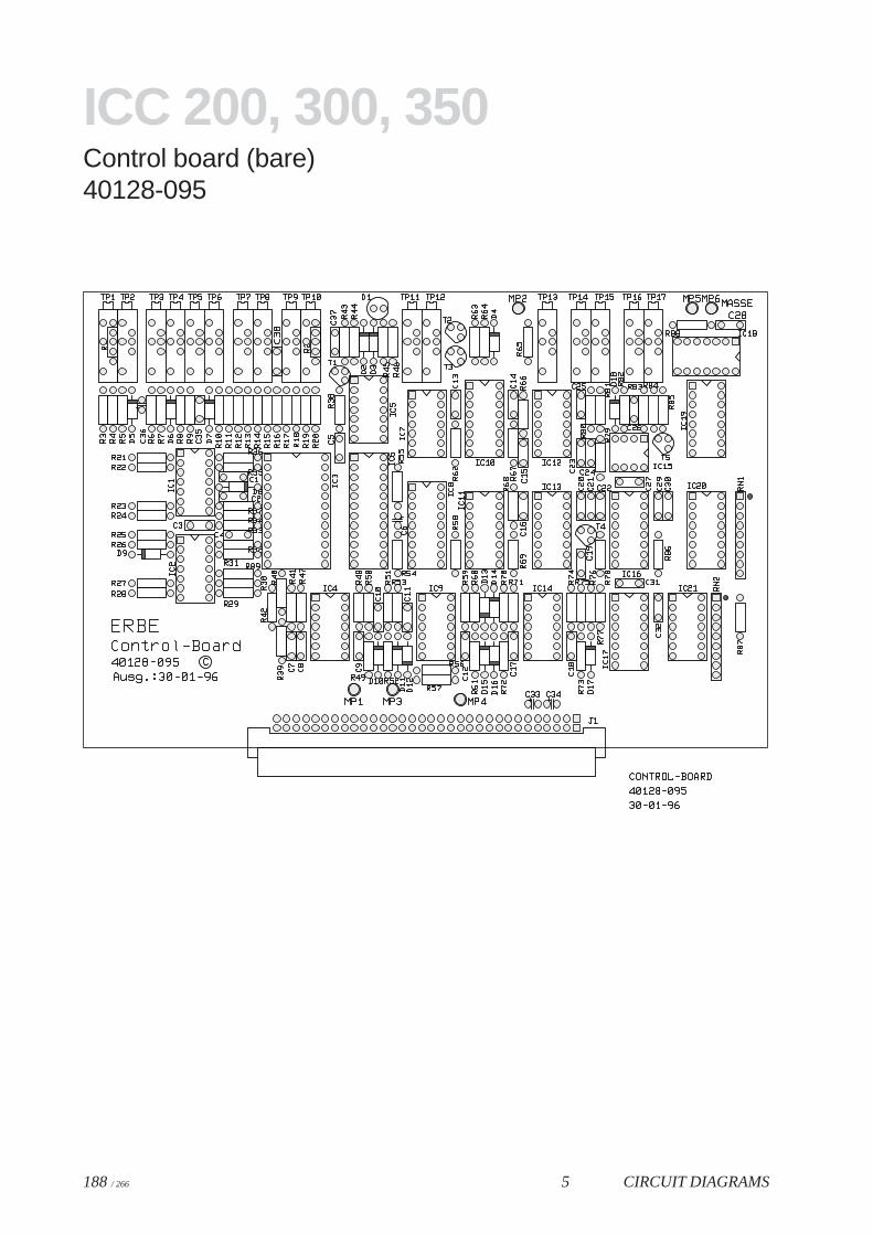
188 / 266 5 CIRCUIT DIAGRAMS
ICC 200, 300, 350Control board (bare)40128-095
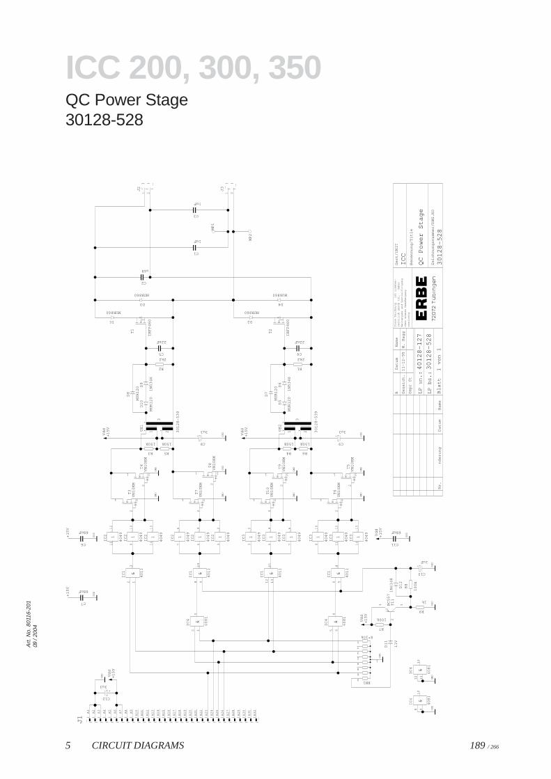
5 CIRCUIT DIAGRAMS 189 / 266
Art
. No.
801
16-2
0109
/ 20
04
ICC 200, 300, 350QC Power Stage30128-528
11
Die
se Z
eic
hn
un
gis
t u
rhe
be
r-
oh
ne
un
sere
Ge
ne
hm
igu
ng
Be
ne
nn
un
g/T
itle
Ze
ich
nu
ng
snu
mm
er/
DW
G.N
O
Ge
rt/U
NIT
We
iterg
ab
e u
nd
Ve
rvie
lfltig
un
gre
chtli
ch g
esc
htz
t,d
ah
er
un
zuls
sig
Da
tum
Na
me
Ge
zeic
h.
Ge
pr
ft
LP
un
.:
LP
bs.
:
Bla
ttvo
nD
atu
mN
am
en
de
run
g
QC
Po
we
r S
tag
e
M. H
ag
g
Nr.
40
12
8-1
27
30
12
8-5
28
30
12
8-5
28
ICC
11
-12
-95
B
C8
+
3u3
C9
+
3u3
C12
+
3u3
C5
22nF
C4
22nF
C2
u68
C1
1uF
C3
1uF
C7
68nF
C6
68nF
C11
68nF
C10
+
1uF
D8
MU
R1
20 D
9
1N
53
46
D6
1N
53
46
D1
2
1N
41
48
D1
0
MU
R1
20 D
7
MU
R1
20
D5
MU
R1
20
D1
MUR860
D3
MUR860
D2
MUR860
D4
MUR860
D1
1
11
V
&
IC1
40
11
&
IC1
40
11
&
IC1
40
11
&
IC1
40
11
IC2 1
40
49
IC2 1
40
49
IC2 1
40
49
IC2 1
40
49
IC2 1
40
49
IC2 1
40
49
IC3 1
40
49
IC3 1
40
49
IC3 1
40
49
IC3 1
40
49
IC3 1
40
49
IC3 1
40
49
&
IC4
40
81
&
IC4
40
81
&
IC4
40
81
&
IC4
40
81
J1
J2 J3
MP
1
MP
2
R2
2k2
R1
2k2
R3
150R
R5
150R
R4
150R
R6
150R
R7
100k
R9
1k
R8
10
0k
RN1
8*10k
T3
VN
10
KM
T7
VN
10
KM
T1
0V
N1
0K
M
T6
VN
10
KM
T1
IRF
P4
60
T2
IRF
P4
60
T4
VN
10
KM
T8
VN
10
KM
T9
VN
10
KM
T5
VN
10
KM
T1
1B
C5
57
UE
1
30
12
8-5
39
1 2
3
UE
2
30
12
8-5
39
1 2
3
GN
D
GN
D
GN
D
GN
D
GN
D
GN
D
GN
D
GN
D
GN
D
GN
D
GN
D
GN
D
GN
D
GN
D
GN
DG
ND
GN
DG
ND
GN
D
+1
5V
+1
5V
Vd
d
+1
5V
+1
5V
Vd
d
+1
5V
Vd
d
+1
5V
Vd
d
+1
5V
Vd
d
2 13
8 91
0
12
13
11
6 54
11
12
91
0
14
15
76
54
32
32
54
76
91
0
11
12
14
15
5 64
2 13
8 91
01
2
13
11
A1
A1
0
A1
1
A1
2
A1
3
A1
4
A1
5
A1
6
A1
7
A1
8
A1
9
A2
A2
0
A2
1
A2
2
A2
3
A2
4
A2
5
A2
6
A2
7
A2
8
A2
9
A3
A3
0
A3
1
A3
2
A4
A5
A6
A7
A8
A9
1 2 1 2
1
9
6
8
4
2
3
7
5
1
2
3 1
2
3 1
2
3 1
2
3
1
2
3 1
2
3 1
2
3 1
2
3
2
31
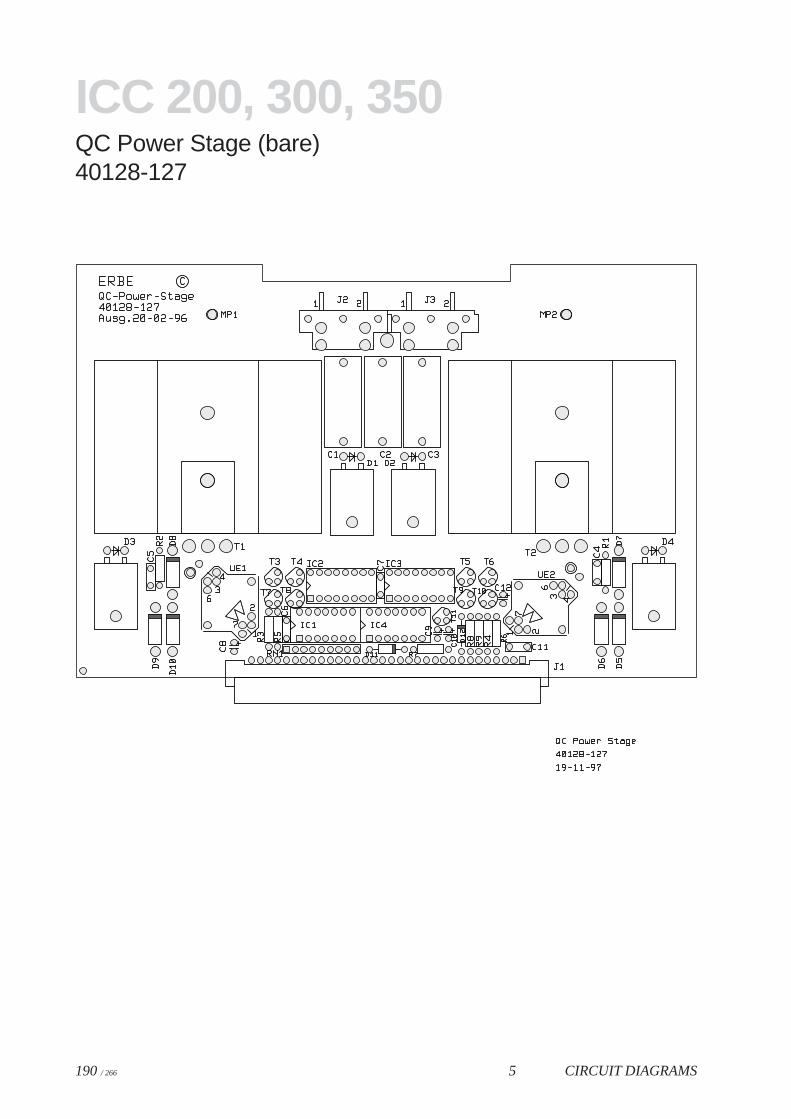
190 / 266 5 CIRCUIT DIAGRAMS
ICC 200, 300, 350QC Power Stage (bare)40128-127
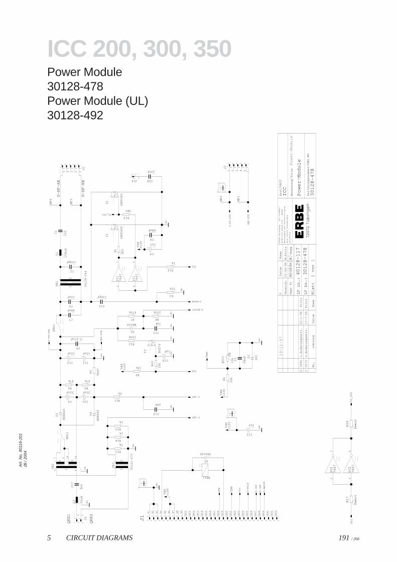
5 CIRCUIT DIAGRAMS 191 / 266
Art
. No.
801
16-2
0109
/ 20
04
ICC 200, 300, 350Power Module30128-478Power Module (UL)30128-492
QK
E1
QK
E2
U-H
F-A
E
U-H
F-N
E
Die
se Z
eic
hn
un
gis
t u
rhe
be
r-
oh
ne
un
sere
Ge
ne
hm
igu
ng
Be
ne
nn
un
g/T
itle
Ze
ich
nu
ng
snu
mm
er/
DW
G.N
O
Ge
rt/U
NIT
We
iterg
ab
e u
nd
Ve
rvie
lfltig
un
gre
chtli
ch g
esc
htz
t,d
ah
er
un
zuls
sig
Da
tum
Na
me
Ge
zeic
h.
Ge
pr
ft
LP
un
.:
LP
bs.
:
Bla
ttvo
nD
atu
mN
am
en
de
run
g
ICC
11
Po
we
r-M
od
ule
40
12
8-1
17
30
12
8-4
78
30
12
8-4
78
M.
Ha
gg
M.F
ritz
Fritz
17
-7-9
5s.
An
de
run
gsm
itt.
35
70
C
Nr.
31
-05
-95
31
-05
-95
s.A
nd
eru
ng
smitt
.F
ritz
D3
69
6
D
22
-1-9
6
2.0
0.8
1.0
C1
7
9n
5
C4
+
22uF
C10
+
22uF
C14
+
10uF
C11
+
10uF
C6
0.47uF
C7
68nF
C5
10nF
C1
1n
5
C2
150pF
C16
u68
C13
1nF
C9
+
3u3
C8
68nF
C15
+
3u3
C3
68
nF
C12
150pF
C28
22nF
C18
+
1uF
D3
MU
R8
60
D4
MU
R8
60
D2
BA159
D5
1N4148
D1
9V
1
76
67
IC1
76
67
IC1
J1
J2 J3
J4
J14
L2
52
uH
L1
15
8u
H
MP
1
MP
4
MP
3 MP
2N
TC
1
10
k
R4
47k
R6
47k
R5
0R
47
R13
1k
R14
1k
R15
1k
R11
2k
R9
10k R1
0
10
k
R12
330R
R7
470k
R8
200k
R1
3R
3
R2
30
k
R3
51k
R19
3R3
R16
1k
RE
L1
RE
L1
REL1
T1
IRF
P4
50
T2
IRF
P4
50
T3
BU
Z7
4
UE
2
1
2 3
UE
1
12
30
12
8-0
44
30
12
1-0
73
UE
3
12
GN
D
GN
D
GN
D
GN
DG
ND
GN
D
GN
D
GN
D
GN
D
GN
D
GN
DG
ND
GN
DG
ND
GN
D-S
TE
GN
D-S
TE
NTE
NT
E
T2_TSI
TE
MP
TE
MP
TS
I
TSI
U-I
NP
U-INP
U-INT
U-I
NT
U-N
ET
ZT
U-NETZT
U-N
T-S
TE
U-N
T-S
TE
U-P
RIM
U-PRIM
+1
5V
Vd
d
+1
5V
Vd
d
+1
5V
Vd
d
+1
5V
Vd
d+
15
VV
dd
72
54
A1
A1
0
A1
1
A1
2
A1
3
A1
4
A1
5
A1
6
A1
7
A1
8
A1
9
A2
A2
0
A2
1
A2
2
A2
3
A2
4
A2
5
A2
6
A2
7
A2
8
A2
9
A3
A3
0
A3
1
A3
2
A4
A5
A6
A7
A8
A9
12345 1 2 3 4 5
12
1
3 4
7 9 10
12
Po
we
r-M
od
ule
40
12
8-1
17
19
-11
-97
c43
0
ec150r ec150r
ec130r ec130r
c225_11
c380
c225_11
c22
5_
6
c100
c150
$plname
$plname
$plname
$plname
$p
lna
me
c100
c150
$plname
d5
0b
10
skk
d5
0b
10
skk
$plname
$plname
$p
lna
me
$p
lna
me
$rp
na
me
$p
lna
me
$rp
na
me
$p
lna
me
$p
lna
me
$p
lna
me
m3schraub
$p
lna
me
$p
lna
me
12
06
$plname $plname
r20
0
r150
r150
r150
$plname
$plname
$p
lna
me
r150
$plname $plname
$p
lna
me
$p
lna
me
$plname
$plname
$plname
$p
lna
me
$rp
na
me
$p
lna
me
$rp
na
me
$plname
$rpname
$p
lna
me
$p
lna
me
$p
lna
me
$p
lna
me
$p
lna
me
$p
lna
me
76
67
IC2
76
67
IC2
R1
7
$w
ert
R1
8
$w
ert
T2
_T
SI
TS
I
72
54
$p
lna
me
$rp
na
me
$p
lna
me
$rp
na
me
$p
lna
me
$p
lna
me
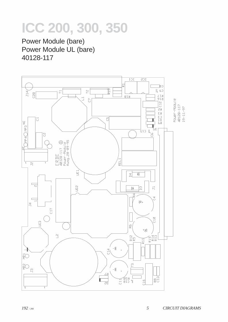
192 / 266 5 CIRCUIT DIAGRAMS
ICC 200, 300, 350Power Module (bare)Power Module UL (bare)40128-117
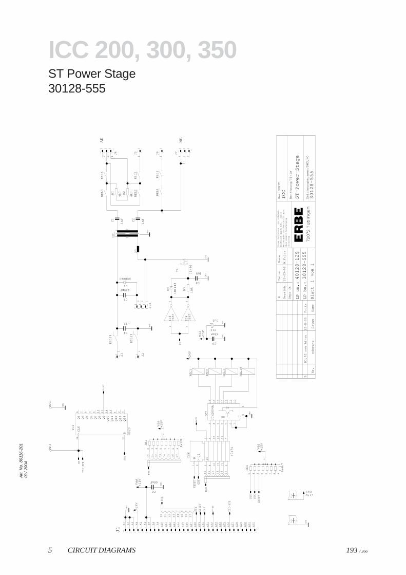
5 CIRCUIT DIAGRAMS 193 / 266
Art
. No.
801
16-2
0109
/ 20
04
ICC 200, 300, 350ST Power Stage30128-555
1
AE
NE
Die
se Z
eic
hn
un
gis
t u
rhe
be
r-
oh
ne
un
sere
Ge
ne
hm
igu
ng
Be
ne
nn
un
g/T
itle
Ze
ich
nu
ng
snu
mm
er/
DW
G.N
O
Ge
rt/U
NIT
We
iterg
ab
e u
nd
Ve
rvie
lfltig
un
gre
chtli
ch g
esc
htz
t,d
ah
er
un
zuls
sig
Da
tum
Na
me
Ge
zeic
h.
Ge
pr
ft
LP
un
.:
LP
bs.
:
Bla
ttvo
nD
atu
mN
am
en
de
run
g
M.F
ritz
1
ICC
Nr.
15
-03
-96
40
12
8-1
29
30
12
8-5
55
30
12
8-5
55
ST
-Po
we
r-S
tag
e
B
B1
2-8
-96
Fritz
R1
,R2
ne
u h
inzu
0.8
0.6
C4
u33
C3
150pF
C9
68nF
C1
1n
F C2
1n
F
C10
+
3u3
C6
68nF
C5
6n8
D4
1N
41
48D1
MUR860
1DR C
1 40
17
4
IC6
Q1
Q4
Q5
Q6
Q7
Q8
Q9
Q1
0
Q1
1
Q1
2
Q1
3
Q1
4R
CL
K
IC1
40
20
IC7
UL
N2
00
4A
76
67
IC4
76
67
IC4
J1J3 J2
J14
J4 J5 J6 J7
L1
MP
3M
P1
R1
4k7 R
2
4k7
R3
10
RR
EL
1
RE
L2
RE
L3
RE
L3
RE
L3
RE
L2
RE
L2
RE
L1
RE
L1
RE
L1
9
RE
L1
9
RE
L1
9
RN
2
8x1
0k
RN
1
8x4
k7
T1
11
N8
0
UE
1
12
CS
3
CS
3
CS
5
CS
5
CS
5
RE
SE
T
RE
SE
T
RE
SE
T
AU
S
AU
S
BU
S
BU
S
BU
S
F-S
T
F-S
T
GN
D
GN
D
GN
DG
ND
GN
D GN
DG
ND
GN
D
GN
D
GN
D
GN
D
+2
4V
+2
4V
SG
SG
TS
I-S
TE
TS
I-S
TE
+1
5V
Vd
d
+1
5V
Vd
d
+1
5V
Vd
d
+1
5V
Vd
d
+15VVdd
D7
D6
D5
D4
D3
D2
D1
D0
D5
D4
D3
D2
D1
D0
D7
D6
D5
D4
D3
D2
D1
D0
1 32
45
14
15
13
12
11
10
67
9
10
9 14
15
1 2 37 5 4 6 13
12
11
3 4 1 2 5 6 7
14
13
16
15
12
11
10
89
72
54
A1
A1
0
A1
1
A1
2
A1
3
A1
4
A1
5
A1
6
A1
7
A1
8
A1
9
A2
A2
0
A2
1
A2
2
A2
3
A2
4
A2
5
A2
6
A2
7
A2
8
A2
9
A3
A3
0
A3
1
A3
2
A4
A5
A6
A7
A8
A9
1 1
123
123 1 1 1 2 3
1
2 3 4 5 6 7 8 9
1
2 4 3 5 6 7 8 9
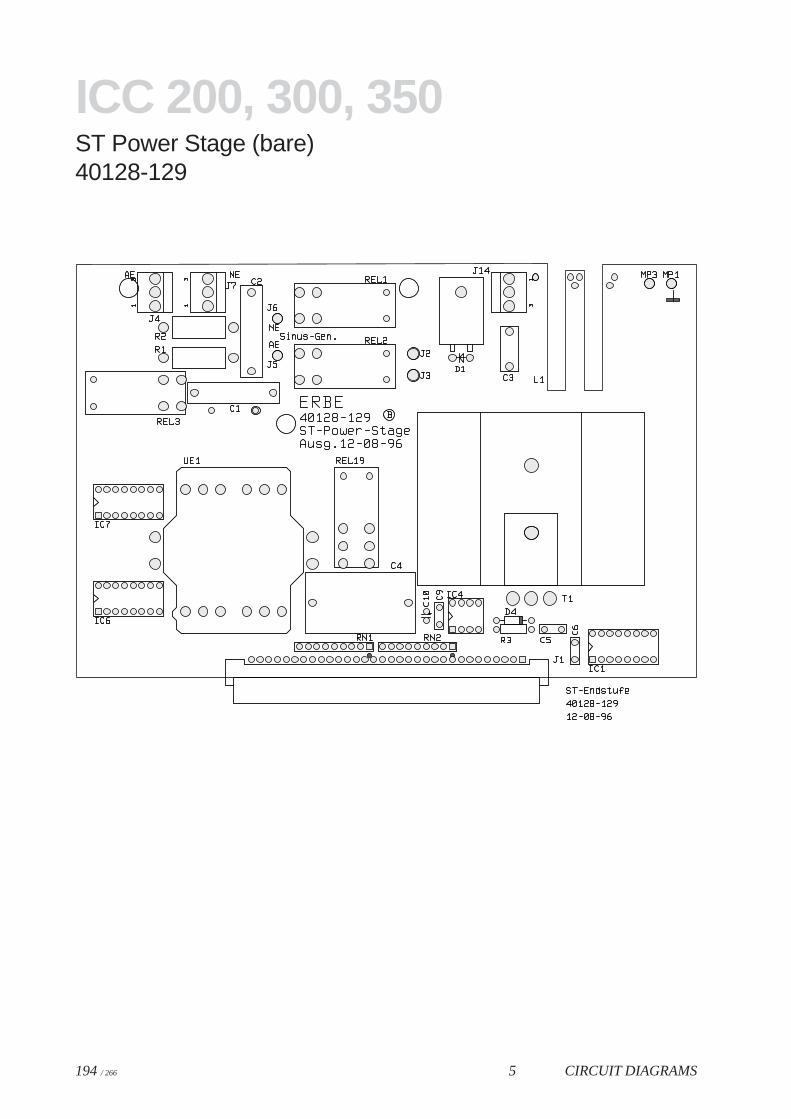
194 / 266 5 CIRCUIT DIAGRAMS
ICC 200, 300, 350ST Power Stage (bare)40128-129
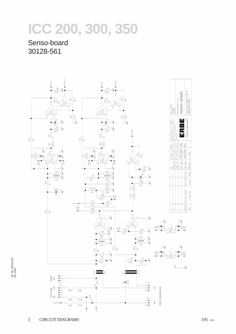
5 CIRCUIT DIAGRAMS 195 / 266
Art
. No.
801
16-2
0109
/ 20
04
ICC 200, 300, 350Senso-board30128-561
AE
NE
AE
BIP
OL
AR
MO
NO
FR
OM
GE
NE
RA
TO
R
AE
NE
1
Die
se Z
eic
hn
un
gis
t u
rhe
be
r-
oh
ne
un
sere
Ge
ne
hm
igu
ng
Be
ne
nn
un
g/T
itle
Ze
ich
nu
ng
snu
mm
er/
DW
G.N
O
Ge
rt/U
NIT
We
iterg
ab
e u
nd
Ve
rvie
lfltig
un
gre
chtli
ch g
esc
htz
t,d
ah
er
un
zuls
sig
Da
tum
Na
me
Ge
zeic
h.
Ge
pr
ft
LP
un
.:
LP
bs.
:
Bla
ttvo
nD
atu
mN
am
en
de
run
g3
SE
NS
O-B
OA
RD
ICC
12
.08
.96
12
.08
.96
FritzFritz
Nr.
30
12
8-5
61
30
12
8-5
61
40
12
8-1
30
B
B4
34
3C
39
ne
u h
inzu
12
-1-9
8F
ritz
C1
1
68
nF
C1
2
68
nF
C13
u22C
32
68
nF
C3
1
68
nF
C1
15
0p
F
C2
8
68
nF
C2
9
68
nF
C30
1nF
C1
4
68
nF
C1
5
68
nF
C33
1nF
C27
220pF
D18
1N4148
D19
1N4148
D17
1N4148
D16
1N4148
D2
0
1N
41
48
D2
1
1N
41
48
D2
6
1N
41
48
D2
7
1N
41
48
D1
0
1N
41
48
D2
3
1N
41
48
D28
1N4148
D29
1N4148
D31
1N4148
D32
1N4148
D22
1N4148
D33
15VIC
3
+- LM
31
9G
ND
-+
IC3
LM
31
9
IC3
+- LM
31
9G
ND
IC8
+ -TL
08
4
IC8
+- TL
08
4
IC8
+- TL
08
4
-+
IC8
TL
08
4
IC4
+-+
- AD
84
4T
ZO
FF
IC7
+-+
- AD
84
4T
ZO
FF
IC8
+ -TL
08
4
IC9
+ -TL
08
4
J2
J1J3
J5
J8
J10
J9
J7
MP
1
R5
0
10
k
R61
4k7
R5
1
10
k
R64
4k7
R65
4k7
R74
3M3
R11
1k
R16
2k
R2
2
10
k
R15
2k
R23
560R
R2
0
18
k
R40
1k3
R13
10R
R14
10k
R5
5
4k7
R4
7
2k
R4
8
1k
R49
1M
R3
6
7k5
R25
2k
R5
4
1k
R53
1M
R5
2
7k5
R1
7
7k5
R24
2k
R12
1k
R2
1
7k5
R38
470R
R67
10k
R6
2
75
0R
R6
3
6k8 R
39
6k8
R3
7
75
0R
REL1REL1
REL3REL3
REL2REL2
BS
17
0
T3
1:5
0
UE
1
12
UE
2
10
0:8
12
AE
GN
D
GN
D
GN
D
GN
D
GN
D
GN
DG
ND
GN
D
GN
DG
ND
GN
DG
ND
GN
D
GN
DG
ND
GN
DG
ND
GN
D
GN
DG
ND
GN
DG
ND
GN
DG
ND
GN
D
GN
DG
ND
GN
DG
ND
GN
DG
ND
GN
DG
ND
GN
D
GN
D
GN
D
GN
D
GN
DG
ND
GN
D
IP_
PA
T
IP_
PA
T_
A
NE
NE_NESSY
TEILERU
_P
HA
SE
UP
_H
F
UP
_H
F_
A
+1
5V
Vd
d
+1
5V
Vd
d
+1
5V
Vd
d
+1
5V
Vd
d
+1
5V
Vd
d+
15
VV
dd
Ve
e-1
5V
Ve
e-1
5V
Ve
e-1
5V
Ve
e-1
5V
Ve
e-1
5V
Ve
e-1
5V
10
89
7
611
5
34
12
9
10
8
6 5
7
13
12
14
11
4
2 3
4
6
18
7
5
2 3
4
6
18
7
5
23
1
23
1
1
2
3
1
2
3
1
2
3
1
2
3
4
5
3
2
1
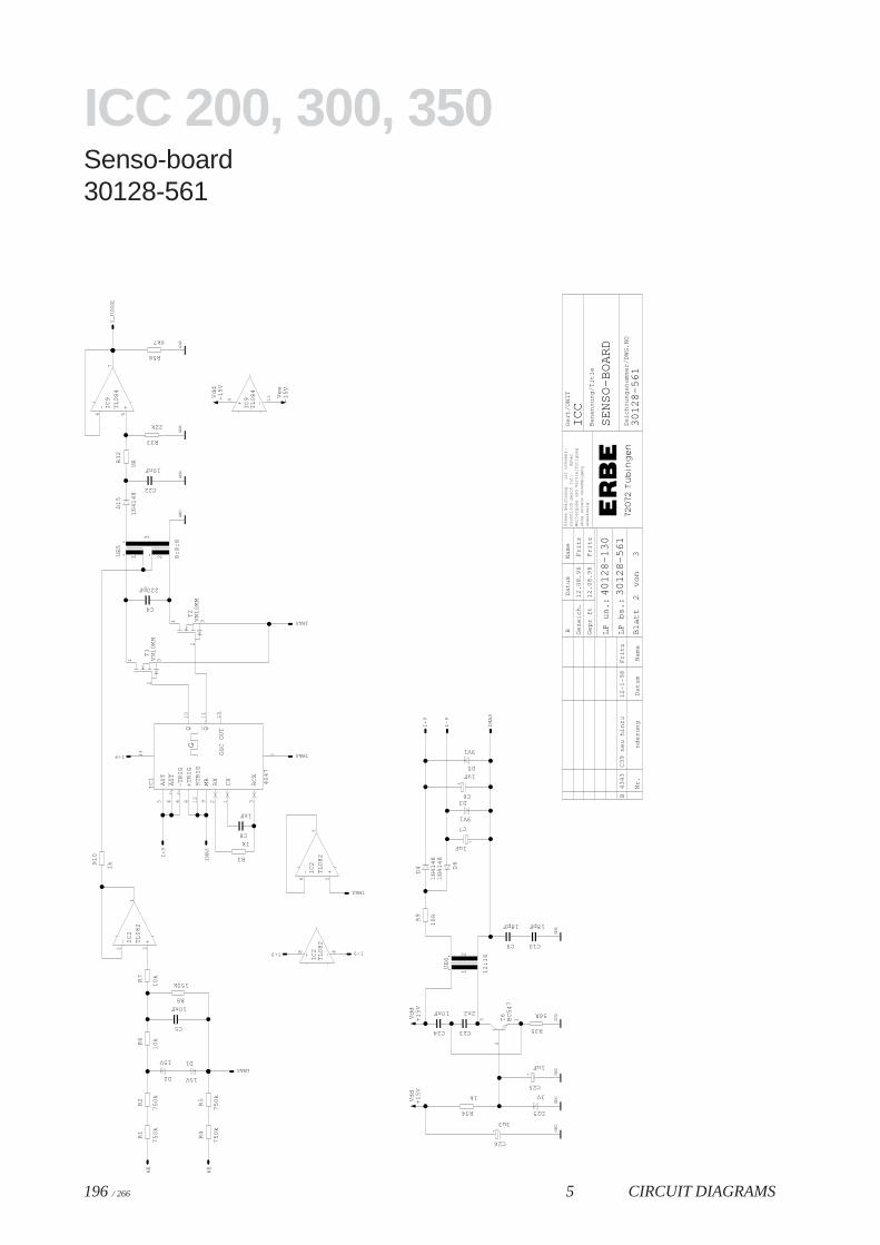
196 / 266 5 CIRCUIT DIAGRAMS
ICC 200, 300, 350Senso-board30128-561
2
Die
se Z
eic
hn
un
gis
t u
rhe
be
r-
oh
ne
un
sere
Ge
ne
hm
igu
ng
Be
ne
nn
un
g/T
itle
Ze
ich
nu
ng
snu
mm
er/
DW
G.N
O
Ge
rt/U
NIT
We
iterg
ab
e u
nd
Ve
rvie
lfltig
un
gre
chtli
ch g
esc
htz
t,d
ah
er
un
zuls
sig
Da
tum
Na
me
Ge
zeic
h.
Ge
pr
ft
LP
un
.:
LP
bs.
:
Bla
ttvo
nD
atu
mN
am
en
de
run
g3
SE
NS
O-B
OA
RD
ICC
12
.08
.96
12
.08
.96
FritzFritz
Nr.
30
12
8-5
61
30
12
8-5
61
40
12
8-1
30
B
B4
34
3C
39
ne
u h
inzu
12
-1-9
8F
ritz
C4
220pF
C22
10nF
C26
+
3u3
C25
+
1uF
C23
2n2
C24
10nF
C7
+
1uF
C6
+
1uF
C10
18pF
C9
18pF
C5
10nF
C8
1nF
D1
15VD2
15V
D1
5
1N
41
48
D25
3V
D4
1N
41
48
D6
1N
41
48
D3
9V1
D5
9V1
IC2
+- TL
08
2
-+
IC2
TL
08
2
RC
X
CX
Q Q
IC1 AS
T
-TR
IG
+T
RIG
RT
RIG
MR
RX
AS
T
OS
C O
UT
G
40
47
IC2
+- TL
08
2
IC9
+- TL
08
4
-+
IC9
TL
08
4
R1
75
0k
R2
75
0k
R4
75
0k
R5
75
0k
R6
10
k
R8
150kR7
10
k
R1
0
1k
R3
1k
R3
2
0R
R33
22k
R34
1k
R35
56R
R9
10
R
R58
4k7
T2
VN
10
KM
T1
VN
10
KM
T6
BC
54
7
12
:16
UE
6
12
UE
5
8:8
:8
1 2
3A
E
GN
DG
ND
GN
D
GN
D
GN
DG
ND
GN
DG
ND
GN
D
I+9
I+9
I+9
I+9
I-9
I-9
IMAS
IMAS
IMA
S
IMAS
IMA
S
IMAS
NE
U_
FU
NK
E
+1
5V
Vd
d+
15
VV
dd
+1
5V
Vd
d
Ve
e-1
5V
2 3
1
48
864
11
5 1
14
7
9
13
10
312
2
6 5
7
6 5
7
11
4
1
2
3
1
2
3
2
3 1
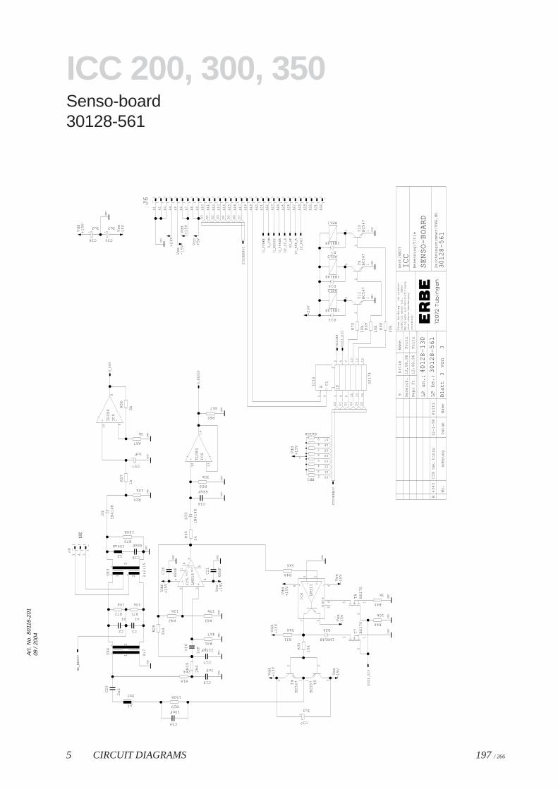
5 CIRCUIT DIAGRAMS 197 / 266
Art
. No.
801
16-2
0109
/ 20
04
ICC 200, 300, 350Senso-board30128-561
3
NE
Die
se Z
eic
hn
un
gis
t u
rhe
be
r-
oh
ne
un
sere
Ge
ne
hm
igu
ng
Be
ne
nn
un
g/T
itle
Ze
ich
nu
ng
snu
mm
er/
DW
G.N
O
Ge
rt/U
NIT
We
iterg
ab
e u
nd
Ve
rvie
lfltig
un
gre
chtli
ch g
esc
htz
t,d
ah
er
un
zuls
sig
Da
tum
Na
me
Ge
zeic
h.
Ge
pr
ft
LP
un
.:
LP
bs.
:
Bla
ttvo
nD
atu
mN
am
en
de
run
g3
SE
NS
O-B
OA
RD
ICC
12
.08
.96
12
.08
.96
FritzFritz
Nr.
30
12
8-5
61
30
12
8-5
61
40
12
8-1
30
B
B4
34
3C
39
ne
u h
inzu
12
-1-9
8F
ritz
C2
u1
C3
u1
C57
+
1uF
C2
0
2n
2
C19
1nF
C1
6
1n
F
C1
8
68
nF
C2
1
68
nF
C37
+
3u3
C34
68nF
C36
+
3u3
C35
+
3u3
C17
220pF
C38
68nF
C39
10nF
D9
1N
41
48
D24
1N4148
D3
0
1N
41
48
D13
1N4148
D14
1N4148
D7
1N4148
IC9
+ -TL
08
4
IC5
+-+
- LM
31
8B
/C3C2
B/C
1
+ -
IC6
+-L
M3
11
BB
/S
IC9
+ -TL
08
4
1DR C
1 40
17
4
IC1
0
J6
J4
L1
3m3
L2
100uH
R42
12k
R43
10k
R57
3k
R66
4k7
R72
10k
R71
10k
R73
100R
R26
10k
R2
7
1k
R5
6
3k
R18
2k4
R29
150R
R1
9
2k4
R6
0
1k
R3
0
10
k
R31
5k6
R44
5k6
R45
1k
R46
10k
R59
30k
R6
8
10
kR6
9
10
kR7
0
10
k
R41
4k7R2
8
2k4
REL1
REL3
REL2
RN1
8x10k
T4
BC
54
7
BC
55
7 T5
BS
17
0
T7
BS
17
0
T8
T9
BC
54
7T
10
BC
54
7T
11
BC
54
7
UE
3
2:2
:15
1 2
3
UE
4
9:7
12
GN
D
GN
DG
ND
GN
DG
ND
GN
DG
ND
GN
DG
ND
GN
D
GN
DG
ND
GN
D
GN
D
GN
DG
ND
GN
D
GN
DG
ND
GN
D
GN
D
GN
D
GN
D
IP_
PA
T
IP_
PA
T_
A
NE
_N
ES
SY
OS
ZI_
DIS
OS
ZI_
DIS
+2
4V
+2
4V
ST
EU
ER
BU
S
ST
EU
ER
BU
ST
EIL
ER
U_
FU
NK
E
U_
NE
SS
Y
U_
NE
SS
Y
U_
PH
AS
E
U_
SY
M
U_
SY
M
UP
_H
F
UP
_H
F_
A
Vcc
+5
V
+1
5V
Vd
d
+1
5V
Vd
d
+1
5V
Vd
d
+1
5V
Vd
d
+1
5V
Vd
d
+1
5V
Vd
d
+1
5V
Vd
d
Ve
e-1
5V
Ve
e-1
5V
Ve
e-1
5V
Ve
e-1
5V
Ve
e-1
5V
Ve
e-1
5V
D7
D6
D5
D4
D3
D2
D1
D0
D7
D6
D5
D4
D3
D2
D1
D0
D5
D4
D3
D2
D1
D0
9
10
8
21
8
53
4
6
7
3
56
7 12
48
13
12
14
1 32
45
67
11
10
13
12
14
15
9
A1
A1
0
A1
1
A1
2
A1
3
A1
4
A1
5
A1
6
A1
7
A1
8
A1
9
A2
A2
0
A2
1
A2
2
A2
3
A2
4
A2
5
A2
6
A2
7
A2
8
A2
9
A3
A3
0
A3
1
A3
2
A4
A5
A6
A7
A8
A9
1 2 3
1
2
3
4
5
6
7
8
9
2
3 1
2
31
3
2
1
3
2
1
2
3 1
2
3 1
2
3 1
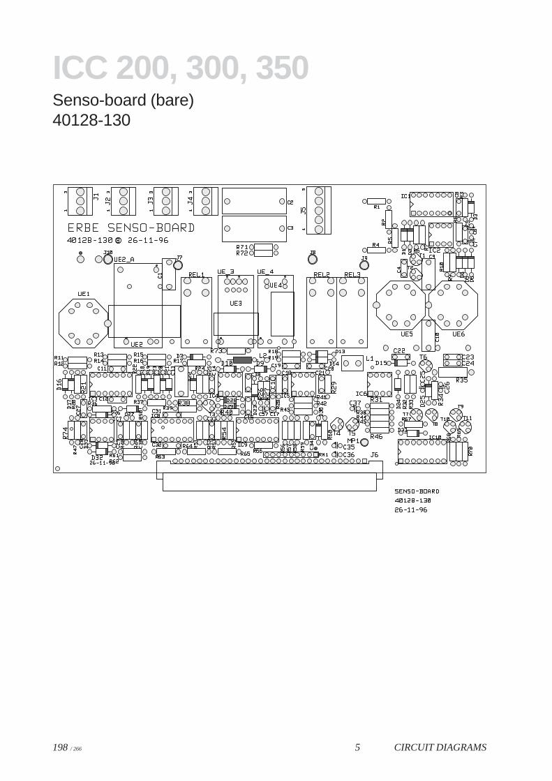
198 / 266 5 CIRCUIT DIAGRAMS
ICC 200, 300, 350Senso-board (bare)40128-130
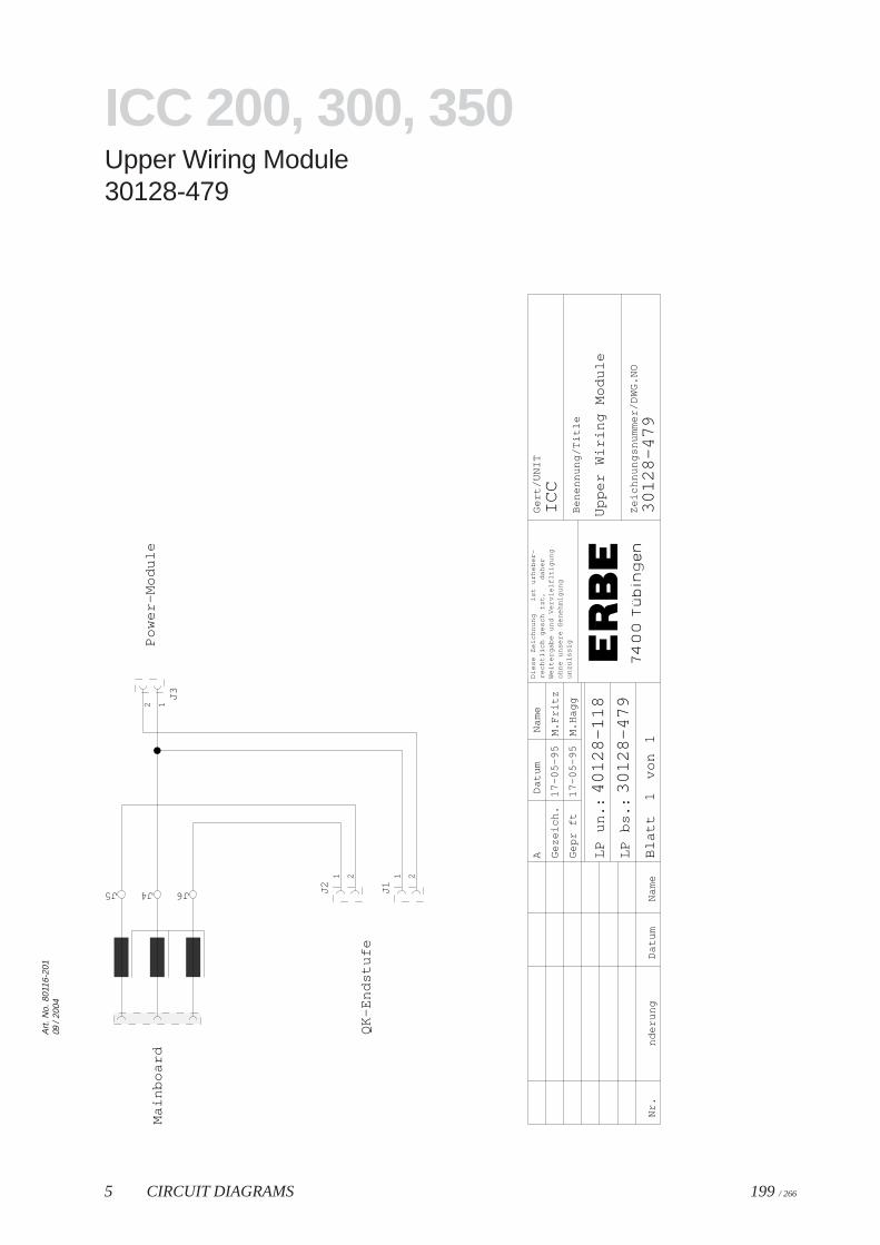
5 CIRCUIT DIAGRAMS 199 / 266
Art
. No.
801
16-2
0109
/ 20
04
ICC 200, 300, 350Upper Wiring Module30128-479
M.F
ritz
11
QK
-En
dst
ufe
Ma
inb
oa
rdP
ow
er-
Mo
du
le
40
12
8-1
18
30
12
8-4
79
30
12
8-4
79
ICC
Up
pe
r W
irin
g M
od
ule
17
-05
-95
17
-05
-95
M.H
ag
g
Die
se Z
eic
hn
un
gis
t u
rhe
be
r-
oh
ne
un
sere
Ge
ne
hm
igu
ng
Be
ne
nn
un
g/T
itle
Ze
ich
nu
ng
snu
mm
er/
DW
G.N
O
Ge
rt/U
NIT
We
iterg
ab
e u
nd
Ve
rvie
lfltig
un
gre
chtli
ch g
esc
htz
t,d
ah
er
un
zuls
sig
Da
tum
Na
me
Ge
zeic
h.
Ge
pr
ft
LP
un
.:
LP
bs.
:
Bla
ttvo
nD
atu
mN
am
en
de
run
gN
r.
A
J1J2
J3
J4J5 J6
1 21 2
12
200 / 266 5 CIRCUIT DIAGRAMS
ICC 200, 300, 350Upper Wiring Module (bare)40128-118

PCBsonly for ICC 200

202 / 266 5 CIRCUIT DIAGRAMS
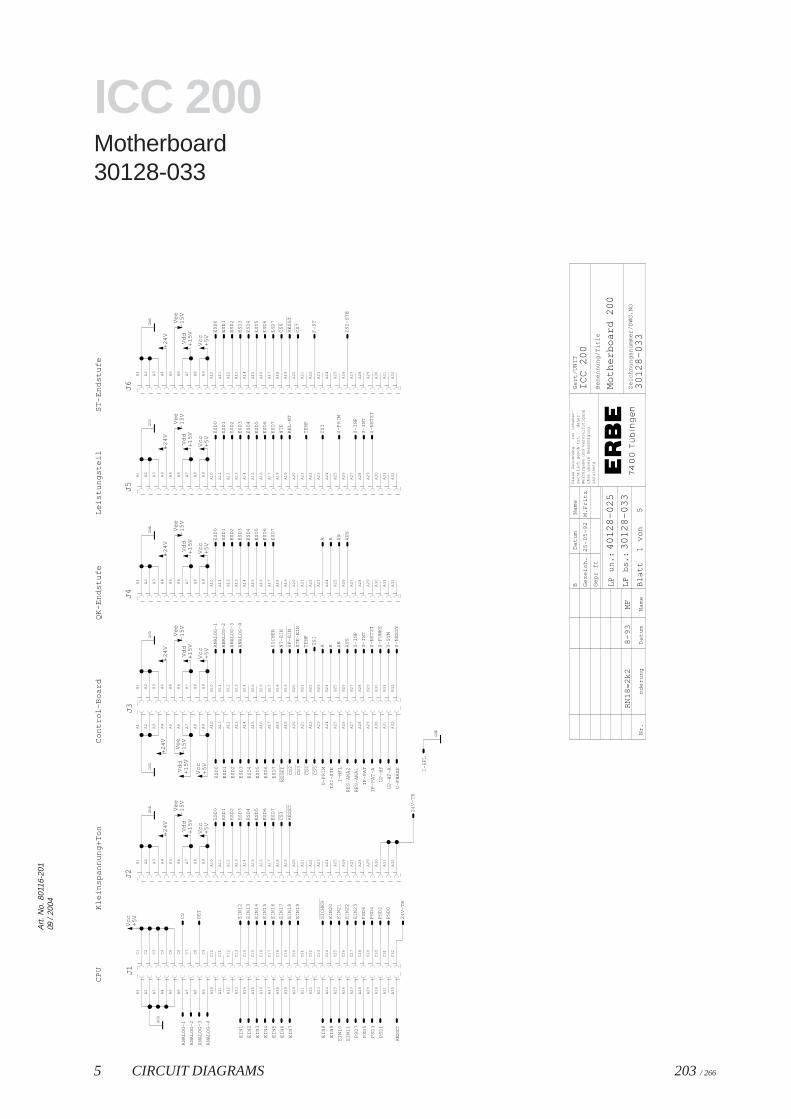
5 CIRCUIT DIAGRAMS 203 / 266
Art
. No.
801
16-2
0109
/ 20
04
ICC 200Motherboard30128-033
1
CP
UK
lein
spa
nn
un
g+
To
nS
T-E
nd
stu
feL
eis
tun
gst
eil
QK
-En
dst
ufe
Co
ntr
ol-B
oa
rd
Die
se Z
eic
hn
un
gis
t u
rhe
be
r-
oh
ne
un
sere
Ge
ne
hm
igu
ng
Be
ne
nn
un
g/T
itle
Ze
ich
nu
ng
snu
mm
er/
DW
G.N
O
Ge
rt/U
NIT
We
iterg
ab
e u
nd
Ve
rvie
lfltig
un
gre
chtli
ch g
esc
htz
t,d
ah
er
un
zuls
sig
Da
tum
Na
me
Ge
zeic
h.
Ge
pr
ft
LP
un
.:
LP
bs.
:
Bla
ttvo
nD
atu
mN
am
en
de
run
gN
r.5
ICC
20
0
40
12
8-0
25
30
12
8-0
33
30
12
8-0
33
Mo
the
rbo
ard
20
0
M.F
ritz
25
-05
-92
B
RN
18
=2
k28
-93
MF
J1J2
J3J4
J5J6
CS
1
CS
2
CS
3
CS
4
CS
5
CS
6
CS
7
HF
-EIN
RE
SE
T
RE
SE
T
RE
SE
T
SIC
HE
R
ST
E-E
IN
24
V-T
R
24
V-T
R
AA
AN
AN
AN
AL
OG
-1
AN
AL
OG
-1
AN
AL
OG
-2
AN
AL
OG
-2
AN
AL
OG
-3
AN
AL
OG
-3
AN
AL
OG
-4
AN
AL
OG
-4
AU
SA
US
BB
CS
EIN
1
EIN
10
EIN
11
EIN
12
EIN
13
EIN
14
EIN
15
EIN
16
EIN
17
EIN
18
EIN
19
EIN
2
EIN
20
EIN
21
EIN
22
EIN
23
EIN
3
EIN
4
EIN
5
EIN
6
EIN
7
EIN
8
EIN
9
ES
D0
ES
D0
ES
D0
ES
D0
ES
D0
ES
D1
ES
D1
ES
D1
ES
D1
ES
D1
ES
D2
ES
D2
ES
D2
ES
D2
ES
D2
ES
D3
ES
D3
ES
D3
ES
D3
ES
D3
ES
D4
ES
D4
ES
D4
ES
D4
ES
D4
ES
D5
ES
D5
ES
D5
ES
D5
ES
D5
ES
D6
ES
D6
ES
D6
ES
D6
ES
D6
ES
D7
ES
D7
ES
D7
ES
D7
ES
D7
F-S
T
GN
D
GN
D
GN
DG
ND
GN
DG
ND
GN
DG
ND
I-H
FL I-
HF
L
IP-P
AT
IP-P
AT
-A
NT
-EIN
NT
E
+2
4V
+2
4V
+2
4V
+2
4V
+2
4V
+2
4V
PS
D0
PS
D1
PS
D2
PS
D3
PS
D4
PS
D5
PS
D6
PS
D7
RE
L-N
T
RE
S-A
NA
1
RE
S-A
NA
2
RE
SE
T
SE
T
SIC
HE
R
TE
MP
TE
MP
TS
I
TS
I
TS
I-S
TE
TS
I-S
TE
U-F
UN
KE
U-I
NP
U-I
NP
U-I
NT
U-I
NT
U-N
ES
SY
U-N
ET
ZT
U-N
ET
ZT
U-P
HA
SE
U-P
RIM
U-P
RIM
U-S
YM
UP
-HF
UP
-HF
-A
Vcc
+5
V
Vcc
+5
VV
cc+
5V
Vcc
+5
VV
cc+
5V
Vcc
+5
VV
cc+
5V
+1
5V
Vd
d+
15
VV
dd
+1
5V
Vd
d+
15
VV
dd
+1
5V
Vd
d+
15
VV
dd
Ve
e-1
5V
Ve
e-1
5V
Ve
e-1
5V
Ve
e-1
5V
Ve
e-1
5V
Ve
e-1
5V
A1
A1
0
A1
1
A1
2
A1
3
A1
4
A1
5
A1
6
A1
7
A1
8
A1
9
A2
A2
0
A2
1
A2
2
A2
3
A2
4
A2
5
A2
6
A2
7
A2
8
A2
9
A3
A3
0
A3
1
A3
2
A4
A5
A6
A7
A8
A9
C1
C1
0
C1
1
C1
2
C1
3
C1
4
C1
5
C1
6
C1
7
C1
8
C1
9
C2
C2
0
C2
1
C2
2
C2
3
C2
4
C2
5
C2
6
C2
7
C2
8
C2
9
C3
C3
0
C3
1
C3
2
C4
C5
C6
C7
C8
C9
A1
A1
0
A1
1
A1
2
A1
3
A1
4
A1
5
A1
6
A1
7
A1
8
A1
9
A2
A2
0
A2
1
A2
2
A2
3
A2
4
A2
5
A2
6
A2
7
A2
8
A2
9
A3
A3
0
A3
1
A3
2
A4
A5
A6
A7
A8
A9
A1
A1
0
A1
1
A1
2
A1
3
A1
4
A1
5
A1
6
A1
7
A1
8
A1
9
A2
A2
0
A2
1
A2
2
A2
3
A2
4
A2
5
A2
6
A2
7
A2
8
A2
9
A3
A3
0
A3
1
A3
2
A4
A5
A6
A7
A8
A9
B1
B1
0
B1
1
B1
2
B1
3
B1
4
B1
5
B1
6
B1
7
B1
8
B1
9
B2
B2
0
B2
1
B2
2
B2
3
B2
4
B2
5
B2
6
B2
7
B2
8
B2
9
B3
B3
0
B3
1
B3
2
B4
B5
B6
B7
B8
B9
A1
A1
0
A1
1
A1
2
A1
3
A1
4
A1
5
A1
6
A1
7
A1
8
A1
9
A2
A2
0
A2
1
A2
2
A2
3
A2
4
A2
5
A2
6
A2
7
A2
8
A2
9
A3
A3
0
A3
1
A3
2
A4
A5
A6
A7
A8
A9
A1
A1
0
A1
1
A1
2
A1
3
A1
4
A1
5
A1
6
A1
7
A1
8
A1
9
A2
A2
0
A2
1
A2
2
A2
3
A2
4
A2
5
A2
6
A2
7
A2
8
A2
9
A3
A3
0
A3
1
A3
2
A4
A5
A6
A7
A8
A9
A1
A1
0
A1
1
A1
2
A1
3
A1
4
A1
5
A1
6
A1
7
A1
8
A1
9
A2
A2
0
A2
1
A2
2
A2
3
A2
4
A2
5
A2
6
A2
7
A2
8
A2
9
A3
A3
0
A3
1
A3
2
A4
A5
A6
A7
A8
A9
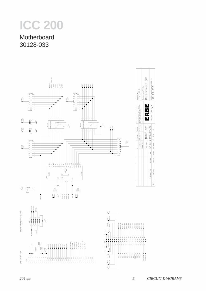
204 / 266 5 CIRCUIT DIAGRAMS
ICC 200Motherboard30128-033
2
To
n J
2
Se
nso
-Bo
ard
Mo
no
-Ou
tpu
t-B
oa
rd
Die
se Z
eic
hn
un
gis
t u
rhe
be
r-
oh
ne
un
sere
Ge
ne
hm
igu
ng
Be
ne
nn
un
g/T
itle
Ze
ich
nu
ng
snu
mm
er/
DW
G.N
O
Ge
rt/U
NIT
We
iterg
ab
e u
nd
Ve
rvie
lfltig
un
gre
chtli
ch g
esc
htz
t,d
ah
er
un
zuls
sig
Da
tum
Na
me
Ge
zeic
h.
Ge
pr
ft
LP
un
.:
LP
bs.
:
Bla
ttvo
nD
atu
mN
am
en
de
run
gN
r.5
ICC
20
0
40
12
8-0
25
30
12
8-0
33
30
12
8-0
33
Mo
the
rbo
ard
20
0
M.F
ritz
25
-05
-92
B
RN
18
=2
k28
-93
MF
C3
68nF
C4
68nF
C24
68nF
0 1 2 3
DM
UX
4 65 7 8 9
10
11
12
13
14
15
20
D0 3
G1
50
C2
0
ENIC
4
45
14
IC1
0
UL
N2
00
4A
IC1
1
UL
N2
00
4A
J9
J7J8
R1
10
k R2
10
k
RN8
8*10k
RN9
8*10k
RN15
8*10k
RN16
8*10k
CS
1
CS
10
CS
11
CS
11
CS
12
CS
12
CS
2
CS
3
CS
4
CS
5
CS
6
CS
7
CS
8
CS
8
CS
9
RE
SE
T
RE
SE
T
RE
SE
T
CS
CS
13
CS
14
ES
D0
ES
D0
ES
D1
ES
D1
ES
D2
ES
D2
ES
D3
ES
D3
ES
D4
ES
D4
ES
D5
ES
D5
ES
D6
ES
D6
ES
D7
ES
D7
FIN
G-A
1
FIN
G-A
3
FIN
G-B
1
FIN
G-B
3
GN
D
GN
D
GN
DG
ND
GN
D
GN
DG
ND
GN
D
GN
D
IP-P
AT
IP-P
AT
-A
+2
4V
+2
4V +2
4V
+2
4V
PS
D0
PS
D1
PS
D2
PS
D3
RE
LA
IS
RE
S-A
NA
1
RE
S-A
NA
2
RE
S-B
1
RE
S-B
2
RE
S-B
3
RE
S-B
4
RE
S-B
5
RE
S-B
6
RE
S-F
1
RE
S-F
2
RE
S-F
3
RE
S-F
4
RE
S-F
5
RE
SE
T
SE
T
U-F
UN
KE
U-N
ES
SY
U-P
HA
SE
U-S
YM
UP
-HF
UP
-HF
-A
Vcc
+5
V
Vcc
+5
VV
cc+
5V
Vcc
+5
V
Vcc
+5
V
Vcc
+5
VV
cc+
5V
Vcc
+5
V
Vcc
+5
V
+1
5V
Vd
d
+1
5V
Vd
d
+1
5V
Vd
d+
15
VV
dd
+1
5V
Vd
d
+1
5V
Vd
d+
15
VV
dd
Ve
e-1
5V
Ve
e-1
5V
Ve
e-1
5V
23
2 3 21
22
1
11
9 20
19
14
13
16
15
10
8 7 6 5 4 18
17
1 2 3 4 5 6 7
16
15
14
13
12
11
10
89
1 2 3 4 5 6 7
16
15
14
13
12
11
10
89
1
10
11
12
13
14
15
16
17
18
19
2
20
21
22
23
24
25
26
27
28
29
3
30
31
32
33
34
35
36
37
38
39
4
40
56
78
9
A1
A1
0
A1
1
A1
2
A1
3
A1
4
A1
5
A1
6
A1
7
A1
8
A1
9
A2
A2
0
A2
1
A2
2
A2
3
A2
4
A2
5
A2
6
A2
7
A2
8
A2
9
A3
A3
0
A3
1
A3
2
A4
A5
A6
A7
A8
A9
1
102
34
56
78
9
1
2
3
4
5
6
7
8
9
1
8
9
7
6
5
4
3
2
1
2
3
4
5
6
7
8
9
1
2
3
4
5
6
7
8
9
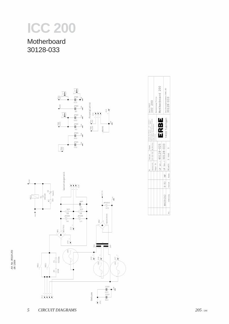
5 CIRCUIT DIAGRAMS 205 / 266
Art
. No.
801
16-2
0109
/ 20
04
ICC 200Motherboard30128-033
3
Ge
hu
se
Le
istu
ng
ste
il
Fro
ntp
latte
Die
se Z
eic
hn
un
gis
t u
rhe
be
r-
oh
ne
un
sere
Ge
ne
hm
igu
ng
Be
ne
nn
un
g/T
itle
Ze
ich
nu
ng
snu
mm
er/
DW
G.N
O
Ge
rt/U
NIT
We
iterg
ab
e u
nd
Ve
rvie
lfltig
un
gre
chtli
ch g
esc
htz
t,d
ah
er
un
zuls
sig
Da
tum
Na
me
Ge
zeic
h.
Ge
pr
ft
LP
un
.:
LP
bs.
:
Bla
ttvo
nD
atu
mN
am
en
de
run
gN
r.5
ICC
20
0
40
12
8-0
25
30
12
8-0
33
30
12
8-0
33
Mo
the
rbo
ard
20
0
M.F
ritz
25
-05
-92
B
RN
18
=2
k28
-93
MF
0.5
0.5
0.5
+-
~ ~
BR
1
BH
37
93
3
+-
~ ~B
R2
B2
50
C5
00
0
C6
+
680uF
C7
+
680uF
C15
+
1000uF
C5
u68
C11
68nF
C22
68nF
C9
68nF
C23
68nF
C8
68nF
C10
68nF
C32
u022
C33
u022
D1
1N
41
48
$w
ertD
2
F1
T2
00
mA
J12
J10
J11
J14
J15
J16
J19
J18
J17
J20
J22
J21
J13
MA
SS
E
R5
10
0R
R6
22k
R9
22k
R3
3k6
RE
L1
RE
L1
RE
L1
TR
1
24
V
Prim.1 Prim.2
Sek.
24
V-T
R
GN
D
GN
DG
ND
GN
DG
ND
GN
DG
ND
GN
D
GN
D
+2
4V
+2
4V
RL
V
Vcc
+5
V
Vcc
+5
V
+1
5V
Vd
d
+1
5V
Vd
d
Ve
e-1
5V
1
1 2 3
1 2 5 6
2361
1
1 1 1
1
1 1
1
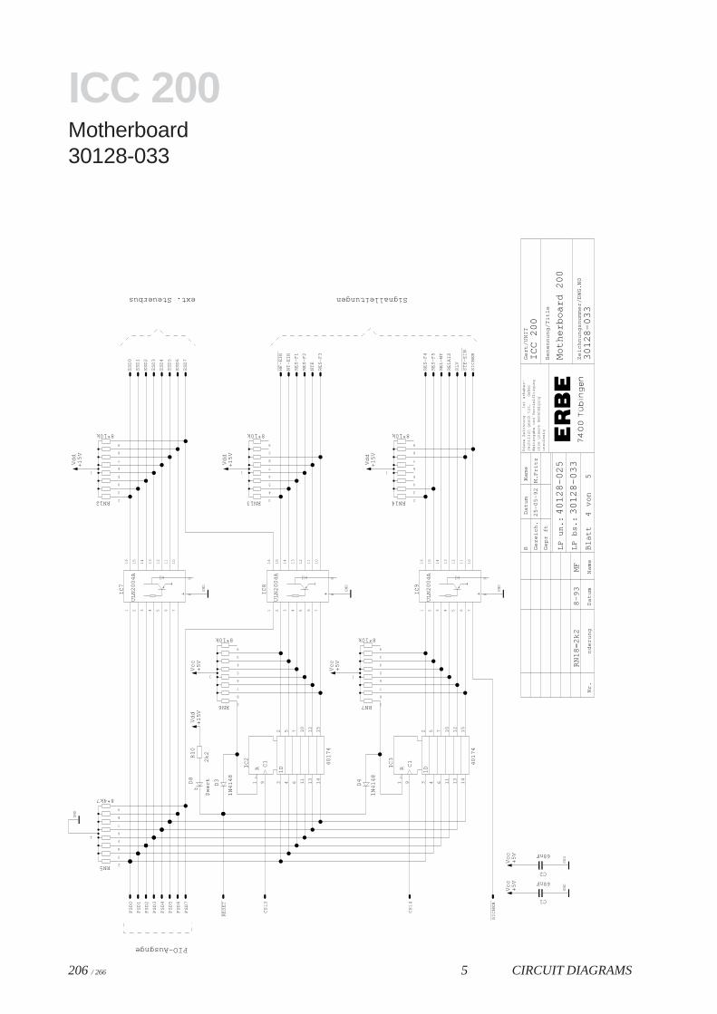
206 / 266 5 CIRCUIT DIAGRAMS
ICC 200Motherboard30128-033
PIO-Ausgnge
Signalleitungenext. Steuerbus
4
Die
se Z
eic
hn
un
gis
t u
rhe
be
r-
oh
ne
un
sere
Ge
ne
hm
igu
ng
Be
ne
nn
un
g/T
itle
Ze
ich
nu
ng
snu
mm
er/
DW
G.N
O
Ge
rt/U
NIT
We
iterg
ab
e u
nd
Ve
rvie
lfltig
un
gre
chtli
ch g
esc
htz
t,d
ah
er
un
zuls
sig
Da
tum
Na
me
Ge
zeic
h.
Ge
pr
ft
LP
un
.:
LP
bs.
:
Bla
ttvo
nD
atu
mN
am
en
de
run
gN
r.5
ICC
20
0
40
12
8-0
25
30
12
8-0
33
30
12
8-0
33
Mo
the
rbo
ard
20
0
M.F
ritz
25
-05
-92
B
RN
18
=2
k28
-93
MF
C1
68nF
C2
68nF
D3
1N
41
48
D4
1N
41
48
$w
ertD
8
1DR C
1 40
17
4
IC2
1DR C
1 40
17
4
IC3
IC7
UL
N2
00
4A
IC8
UL
N2
00
4A
IC9
UL
N2
00
4A
R1
0
2k2
RN5
8*4k7
RN6
8*10k
RN7
8*10k
RN12
8*10k
RN13
8*10k
RN14
8*10k
HF
-EIN
RE
SE
T
SIC
HE
R
ST
E-E
IN
CS
13
CS
14
ES
D0
ES
D1
ES
D2
ES
D3
ES
D4
ES
D5
ES
D6
ES
D7
GN
D
GN
DG
ND
GN
D
GN
D
GN
D
NT
-EIN
NT
E
PS
D0
PS
D1
PS
D2
PS
D3
PS
D4
PS
D5
PS
D6
PS
D7
RE
L-N
T
RE
LA
IS
RE
S-F
1
RE
S-F
2
RE
S-F
3
RE
S-F
4
RE
S-F
5
RL
V
SIC
HE
R
Vcc
+5
V
Vcc
+5
VV
cc+
5V
Vcc
+5
V
+1
5V
Vd
d
+1
5V
Vd
d
+1
5V
Vd
d
+1
5V
Vd
d
1 32
45
67
11
10
13
12
14
15
9 1 32
45
67
11
10
13
12
14
15
9
1 2 3 4 5 6 7
16
15
14
13
12
11
10
89
1 2 3 4 5 6 7
16
15
14
13
12
11
10
89
1 2 3 4 5 6 7
16
15
14
13
12
11
10
89
1
2
3
4
5
6
7
8
9
1
2
8
7
6
5
4
3
9
1
2
8
7
6
5
4
3
9
1
2
3
4
5
6
7
8
9
1
3
4
5
6
7
8
2
9
1
2
3
4
5
6
7
8
9
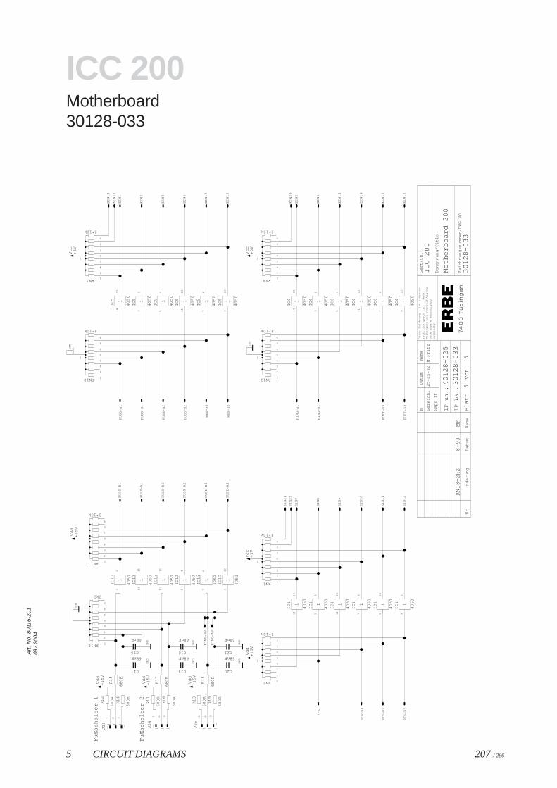
5 CIRCUIT DIAGRAMS 207 / 266
Art
. No.
801
16-2
0109
/ 20
04
ICC 200Motherboard30128-033
5
Fu
Æsc
ha
lter
1
Fu
Æsc
ha
lter
2
Die
se Z
eic
hn
un
gis
t u
rhe
be
r-
oh
ne
un
sere
Ge
ne
hm
igu
ng
Be
ne
nn
un
g/T
itle
Ze
ich
nu
ng
snu
mm
er/
DW
G.N
O
Ge
rt/U
NIT
We
iterg
ab
e u
nd
Ve
rvie
lfltig
un
gre
chtli
ch g
esc
htz
t,d
ah
er
un
zuls
sig
Da
tum
Na
me
Ge
zeic
h.
Ge
pr
ft
LP
un
.:
LP
bs.
:
Bla
ttvo
nD
atu
mN
am
en
de
run
gN
r.5
ICC
20
0
40
12
8-0
25
30
12
8-0
33
30
12
8-0
33
Mo
the
rbo
ard
20
0
M.F
ritz
25
-05
-92
B
RN
18
=2
k28
-93
MF
C19
68nF
C18
68nF
C17
68nF
C16
68nF
C20
68nF
C21
68nF
IC5 1
40
50
IC5 1
40
50
IC5 1
40
50
IC5 1
40
50
IC5 1
40
50
IC5 1
40
50
IC1
3
40
50
1
IC1
3
40
50
1
IC1
3
40
50
1
IC1
3
40
50
1
IC1
3
40
50
1
IC1
3
40
50
1
IC6 1
40
50
IC6 1
40
50
IC6 1
40
50
IC6 1
40
50
IC6 1
40
50
IC6 1
40
50
IC1 1
40
50
IC1 1
40
50
IC1 1
40
50
IC1 1
40
50
IC1 1
40
50
IC1 1
40
50
J24
J23
J25
R1
1
68
0R
R1
7
68
0R
R1
6
68
0R
R1
2
68
0R
R1
5
68
0R
R1
4
68
0R
R1
3
68
0R
R1
8
68
0R
R1
9
68
0R
RN10
8*10k
RN3
8*10k
RN18
2k2
RN17
8*10k
RN11
8*10k
RN4
8*10k
RN2
8*10k
RN1
8*10k
EIN
1
EIN
10
EIN
11
EIN
12
EIN
13
EIN
14
EIN
15
EIN
16
EIN
17
EIN
18
EIN
19
EIN
2
EIN
20
EIN
21
EIN
22
EIN
23
EIN
3
EIN
4
EIN
5
EIN
6
EIN
7
EIN
8
EIN
9
F-S
T
FIN
G-A
1
FIN
G-A
3
FIN
G-B
1
FIN
G-B
3
FU
FI-
A3
FU
FI-
A3
FU
FI-
B3
FU
FI-
B3
FU
SS
-A1
FU
SS
-A1
FU
SS
-A2
FU
SS
-A2
FU
SS
-B1
FU
SS
-B1
FU
SS
-B2
FU
SS
-B2
GN
D
GN
D
GN
DG
ND
GN
DG
ND
GN
DG
ND
GN
D
RE
S-B
1
RE
S-B
2
RE
S-B
3
RE
S-B
5
RE
S-B
6
Vcc
+5
V
Vcc
+5
VV
cc+
5V
+1
5V
Vd
d
+1
5V
Vd
d
+1
5V
Vd
d
+1
5V
Vd
d
+1
5V
Vd
d
14
15
32
54
11
12
76
91
0
32
14
15
11
12
54
76
91
0
14
15
32
54
11
12
76
91
0
14
15
54
11
12
76
91
0
32
1 2 31 2 3 1 2 3
1
2
3
4
5
6
7
8
9
1
2
3
4
5
6
7
8
9
1
5
3
7
6
8
9
4
2
1
2
3
5
4
6
7
8
9
1
2
3
4
5
6
7
8
9
1
2
3
4
5
6
7
8
9
1
9
7
3
5
8
6
2
4
1
3
4
5
7
9
2
8
6
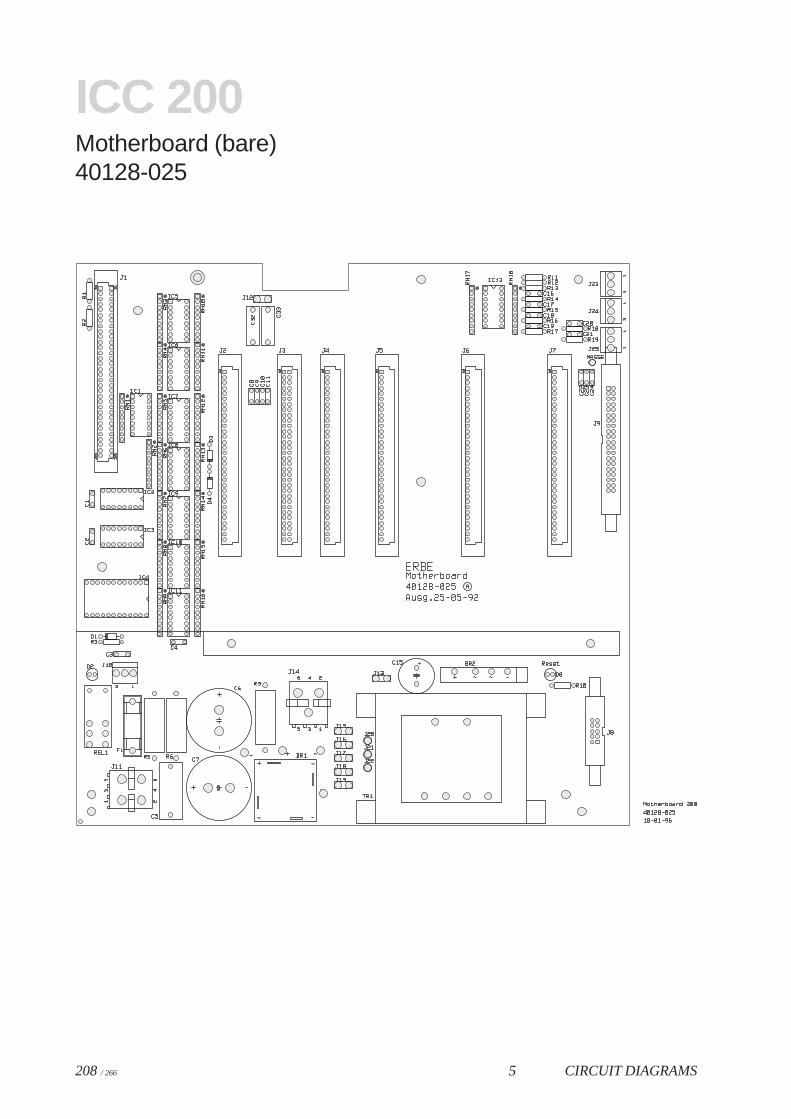
208 / 266 5 CIRCUIT DIAGRAMS
ICC 200Motherboard (bare)40128-025
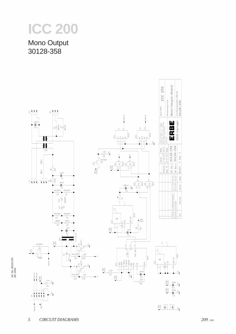
5 CIRCUIT DIAGRAMS 209 / 266
Art
. No.
801
16-2
0109
/ 20
04
ICC 200Mono Output30128-358
Fritz
17
-02
-94
30
12
8-3
58
40
12
8-0
96
30
12
8-3
58
Mo
no
-Ou
tpu
t-B
oa
rd
114
-07
-94
Ha
gg
1
Die
se Z
eic
hn
un
gis
t u
rhe
be
r-
oh
ne
un
sere
Ge
ne
hm
igu
ng
Be
ne
nn
un
g/T
itle
Ze
ich
nu
ng
snu
mm
er/
DW
G.N
O
Ge
rt/U
NIT
We
iterg
ab
e u
nd
Ve
rvie
lfltig
un
gre
chtli
ch g
esc
htz
t,d
ah
er
un
zuls
sig
Da
tum
Na
me
Ge
zeic
h.
Ge
pr
ft
LP
un
.:
LP
bs.
:
Bla
ttvo
nD
atu
mN
am
en
de
run
g
ICC
20
0
31
92
22
.6.9
4F
ritz
B
Nr.
Fritz
C1
1=
10
nF
C3
25
2s.
Ae
nd
eru
ng
smit.
14
.7.9
4
C
0.9
0.6
C11
10nF
C8
+
3u3
C3
1nF
C2
10nF
C1
10nF
C6
68nF
C7
6n8
C5
68nF
C10
68nF
C4
+
3u
3
C9
100pF
D2
BA
15
9
D8
1N4148
D3
1N4148
D4
1N4148
D6
1N4148
D7
1N4148
D9
SD101A
D10
SD101AD
1
BA
15
9D
5
11
V
SFH350
IC1
IC1
SF
H4
50
40
47
RC
X
CX
Q Q
IC2 AS
T
-TR
IG
+T
RIG
RT
RIG
MR
RX
AS
T
OS
C O
UT
G
IC3 CX
R
&
RX
/CX 4
52
8
IC3 CX
R
&
RX
/CX 4
52
8
&
IC5
40
11
&
IC5
40
11
&
IC5
40
11
&
IC5
40
11
S RIC4
D 40
13
C S RIC4
D 40
13
C
J3J1 J2
J5
J4
R11
4k7
R10
4k7
R3
510R
R4
680R
R2
15
0R
R1
56
R
R9
5k1
R5
10k
R6
5k1
R7
4k7
R8
1k
RE
L1
RE
L1
REL1
T2
BC
51
7
T1
BC
51
7UE
2
10
:10
:32
1 2
3
UE1
1
2
3
4
FIN
G_
A1
FIN
G_
A1
FIN
G_
B1
FIN
G_
B1
GN
D
GN
D
GN
D
GN
DG
ND
GN
D
GN
D
GN
D
GN
D
GN
D
GN
DG
ND
GN
D
+2
4V
+2
4V
RE
LA
IS
RE
LA
IS
T1
T1
T2
T2
+1
5V
Vd
d
+1
5V
Vd
d
+1
5V
Vd
d
+1
5V
Vd
d+
15
VV
dd
+1
5V
Vd
d
+1
5V
Vd
d
+1
5V
Vd
d
+15VVdd
+1
5V
Vd
d+
15
VV
dd
B
C
E
864
11
5 19
13
10
312
2
37
5 4 1
6
2
13
9
11
12
15
10
14
8 91
0
12
13
11
6 54
1 23
2
3 4561 1
2
11
10
981
3
1 2 3
1 2 3 123
1
102
34
56
78
9
1 2 3
2
3 1
2
3 1
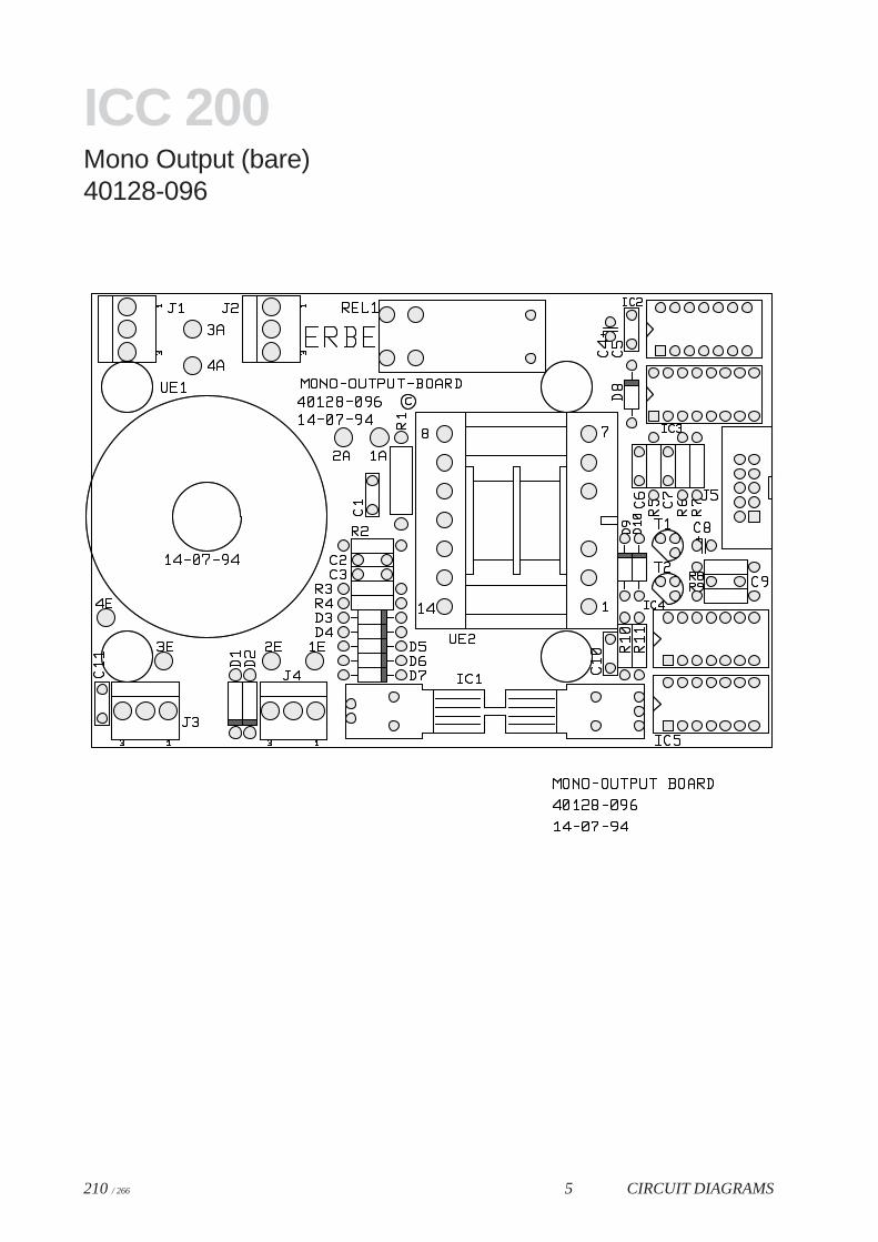
210 / 266 5 CIRCUIT DIAGRAMS
ICC 200Mono Output (bare)40128-096

PCBsonly for ICC 300

212 / 266 5 CIRCUIT DIAGRAMS
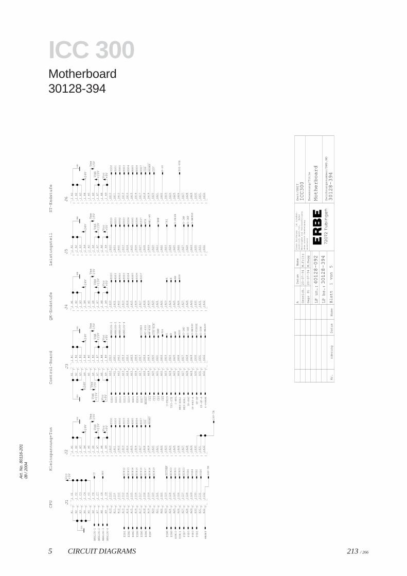
5 CIRCUIT DIAGRAMS 213 / 266
Art
. No.
801
16-2
0109
/ 20
04
ICC 300Motherboard30128-394
1
CP
UK
lein
spa
nn
un
g+
To
nS
T-E
nd
stu
feL
eis
tun
gst
eil
QK
-En
dst
ufe
Co
ntr
ol-B
oa
rd
Die
se Z
eic
hn
un
gis
t u
rhe
be
r-
oh
ne
un
sere
Ge
ne
hm
igu
ng
Be
ne
nn
un
g/T
itle
Ze
ich
nu
ng
snu
mm
er/
DW
G.N
O
Ge
rt/U
NIT
We
iterg
ab
e u
nd
Ve
rvie
lfltig
un
gre
chtli
ch g
esc
htz
t,d
ah
er
un
zuls
sig
Da
tum
Na
me
Ge
zeic
h.
Ge
pr
ft
LP
un
.:
LP
bs.
:
Bla
ttvo
nD
atu
mN
am
en
de
run
gN
r.
M.F
ritz
Mo
the
rbo
ard
A
40
12
8-0
92
20
-07
-94
5
20
-07
-94
M.H
ag
g
30
12
8-3
94
30
12
8-3
94
ICC
30
0
J1J2
J3J4
J5J6
CS
1
CS
2
CS
3
CS
4
CS
5
CS
6
CS
7
HF
-EIN
RE
SE
T
RE
SE
T
RE
SE
T
SIC
HE
R
ST
E-E
IN
24
V-T
R
24
V-T
R
AA
AN
AN
AN
AL
OG
-1
AN
AL
OG
-1
AN
AL
OG
-2
AN
AL
OG
-2
AN
AL
OG
-3
AN
AL
OG
-3
AN
AL
OG
-4
AN
AL
OG
-4
AU
SA
US
BB
CS
EIN
1
EIN
10
EIN
11
EIN
12
EIN
13
EIN
14
EIN
15
EIN
16
EIN
17
EIN
18
EIN
19
EIN
2
EIN
20
EIN
21
EIN
22
EIN
23
EIN
3
EIN
4
EIN
5
EIN
6
EIN
7
EIN
8
EIN
9
ES
D0
ES
D0
ES
D0
ES
D0
ES
D0
ES
D1
ES
D1
ES
D1
ES
D1
ES
D1
ES
D2
ES
D2
ES
D2
ES
D2
ES
D2
ES
D3
ES
D3
ES
D3
ES
D3
ES
D3
ES
D4
ES
D4
ES
D4
ES
D4
ES
D4
ES
D5
ES
D5
ES
D5
ES
D5
ES
D5
ES
D6
ES
D6
ES
D6
ES
D6
ES
D6
ES
D7
ES
D7
ES
D7
ES
D7
ES
D7
F-S
T
GN
D
GN
DG
ND
GN
DG
ND
GN
DG
ND
I-H
FL
IP-P
AT
IP-P
AT
-A
NT
-EIN
NT
E
+2
4V
+2
4V
+2
4V
+2
4V
+2
4V
+2
4V
PS
D0
PS
D1
PS
D2
PS
D3
PS
D4
PS
D5
PS
D6
PS
D7
RE
L-N
T
RE
S-A
NA
1
RE
S-A
NA
2
RE
SE
T
SE
T
SIC
HE
R
TE
MP
TE
MP
TS
I
TS
I
TS
I-S
TE
TS
I-S
TE
U-F
UN
KE
U-I
NP
U-I
NP
U-I
NT
U-I
NT
U-N
ES
SY
U-N
ET
ZT
U-N
ET
ZT
U-P
HA
SE
U-P
RIM
U-P
RIM
U-S
YM
UP
-HF
UP
-HF
-A
Vcc
+5
V
Vcc
+5
VV
cc+
5V
Vcc
+5
VV
cc+
5V
Vcc
+5
VV
cc+
5V
+1
5V
Vd
d+
15
VV
dd
+1
5V
Vd
d+
15
VV
dd
+1
5V
Vd
d+
15
VV
dd
Ve
e-1
5V
Ve
e-1
5V
Ve
e-1
5V
Ve
e-1
5V
Ve
e-1
5V
Ve
e-1
5V
A1
A1
0
A1
1
A1
2
A1
3
A1
4
A1
5
A1
6
A1
7
A1
8
A1
9
A2
A2
0
A2
1
A2
2
A2
3
A2
4
A2
5
A2
6
A2
7
A2
8
A2
9
A3
A3
0
A3
1
A3
2
A4
A5
A6
A7
A8
A9
C1
C1
0
C1
1
C1
2
C1
3
C1
4
C1
5
C1
6
C1
7
C1
8
C1
9
C2
C2
0
C2
1
C2
2
C2
3
C2
4
C2
5
C2
6
C2
7
C2
8
C2
9
C3
C3
0
C3
1
C3
2
C4
C5
C6
C7
C8
C9
A1
A1
0
A1
1
A1
2
A1
3
A1
4
A1
5
A1
6
A1
7
A1
8
A1
9
A2
A2
0
A2
1
A2
2
A2
3
A2
4
A2
5
A2
6
A2
7
A2
8
A2
9
A3
A3
0
A3
1
A3
2
A4
A5
A6
A7
A8
A9
A1
A1
0
A1
1
A1
2
A1
3
A1
4
A1
5
A1
6
A1
7
A1
8
A1
9
A2
A2
0
A2
1
A2
2
A2
3
A2
4
A2
5
A2
6
A2
7
A2
8
A2
9
A3
A3
0
A3
1
A3
2
A4
A5
A6
A7
A8
A9
B1
B1
0
B1
1
B1
2
B1
3
B1
4
B1
5
B1
6
B1
7
B1
8
B1
9
B2
B2
0
B2
1
B2
2
B2
3
B2
4
B2
5
B2
6
B2
7
B2
8
B2
9
B3
B3
0
B3
1
B3
2
B4
B5
B6
B7
B8
B9
A1
A1
0
A1
1
A1
2
A1
3
A1
4
A1
5
A1
6
A1
7
A1
8
A1
9
A2
A2
0
A2
1
A2
2
A2
3
A2
4
A2
5
A2
6
A2
7
A2
8
A2
9
A3
A3
0
A3
1
A3
2
A4
A5
A6
A7
A8
A9
A1
A1
0
A1
1
A1
2
A1
3
A1
4
A1
5
A1
6
A1
7
A1
8
A1
9
A2
A2
0
A2
1
A2
2
A2
3
A2
4
A2
5
A2
6
A2
7
A2
8
A2
9
A3
A3
0
A3
1
A3
2
A4
A5
A6
A7
A8
A9
A1
A1
0
A1
1
A1
2
A1
3
A1
4
A1
5
A1
6
A1
7
A1
8
A1
9
A2
A2
0
A2
1
A2
2
A2
3
A2
4
A2
5
A2
6
A2
7
A2
8
A2
9
A3
A3
0
A3
1
A3
2
A4
A5
A6
A7
A8
A9
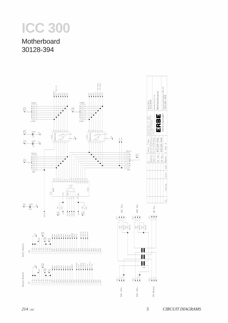
214 / 266 5 CIRCUIT DIAGRAMS
ICC 300Motherboard30128-394
2
To
n J
2
J10
Re
s.
J10
Re
s.
Se
nso
-Bo
ard
Re
fi-B
oa
rd
NE
Bu
.N
E N
ess
y
AE
1 B
u.
AE
2 B
u.
AE
1 G
en
.
AE
2 G
en
.
Die
se Z
eic
hn
un
gis
t u
rhe
be
r-
oh
ne
un
sere
Ge
ne
hm
igu
ng
Be
ne
nn
un
g/T
itle
Ze
ich
nu
ng
snu
mm
er/
DW
G.N
O
Ge
rt/U
NIT
We
iterg
ab
e u
nd
Ve
rvie
lfltig
un
gre
chtli
ch g
esc
htz
t,d
ah
er
un
zuls
sig
Da
tum
Na
me
Ge
zeic
h.
Ge
pr
ft
LP
un
.:
LP
bs.
:
Bla
ttvo
nD
atu
mN
am
en
de
run
gN
r.
M.F
ritz
Mo
the
rbo
ard
A
40
12
8-0
92
20
-07
-94
5
20
-07
-94
M.H
ag
g
30
12
8-3
94
30
12
8-3
94
ICC
30
0
C3
68nF
C4
68nF
C24
68nFD
24
BA
15
9
D2
5
BA
15
9
D2
6
BA
15
9
D2
7
BA
15
9
0 1 2 3
DM
UX
4 65 7 8 9
10
11
12
13
14
15
20
D0 3
G1
50
C2
0
ENIC
4
45
14
IC1
0
UL
N2
00
4A
IC1
1
UL
N2
00
4A
J26
J27
J28
J29
J57
J58
J7J8
R1
10
k R2
10
k
RN8
8*10k
RN9
8*10k
RN15
8*10k
RN16
$wert
UE1
1
2
3
4
5
6
CS
1
CS
10
CS
10
CS
11
CS
11
CS
12
CS
13
CS
2
CS
3
CS
4
CS
5
CS
6
CS
7
CS
8
CS
8
CS
9
CS
9
RE
SE
T
RE
SE
T
RE
SE
T
CS
CS
13
CS
14
ES
D0
ES
D0
ES
D1
ES
D1
ES
D2
ES
D2
ES
D3
ES
D3
ES
D4
ES
D4
ES
D5
ES
D5
ES
D6
ES
D6
ES
D7
ES
D7
FIN
G-A
1
FIN
G-A
2
FIN
G-B
1
FIN
G-B
2
GN
D
GN
D
GN
DG
ND
GN
D
GN
D
GN
D
IP-P
AT
IP-P
AT
-A
+2
4V
+2
4V
PS
D0
PS
D1
PS
D2
PS
D3
RE
SE
T
SE
T
U-F
UN
KE
U-N
ES
SY
U-P
HA
SE
U-S
YM
UP
-HF
UP
-HF
-A
Vcc
+5
V
Vcc
+5
V
Vcc
+5
V
Vcc
+5
VV
cc+
5V
Vcc
+5
V
Vcc
+5
V
Vcc
+5
V
+1
5V
Vd
d
+1
5V
Vd
d
+1
5V
Vd
d+
15
VV
dd
+1
5V
Vd
d
Ve
e-1
5V
Ve
e-1
5V
23
2 3 21
22
1
11
9 20
19
14
13
16
15
10
8 7 6 5 4 18
17
1 2 3 4 5 6 7
16
15
14
13
12
11
10
89
1 2 3 4 5 6 7
16
15
14
13
12
11
10
89
1 2 3
1 2 3
1 2 3 1 2 3
1 2 3 1 2 3
A1
A1
0
A1
1
A1
2
A1
3
A1
4
A1
5
A1
6
A1
7
A1
8
A1
9
A2
A2
0
A2
1
A2
2
A2
3
A2
4
A2
5
A2
6
A2
7
A2
8
A2
9
A3
A3
0
A3
1
A3
2
A4
A5
A6
A7
A8
A9
A1
A1
0
A1
1
A1
2
A1
3
A1
4
A1
5
A1
6
A1
7
A1
8
A1
9
A2
A2
0
A2
1
A2
2
A2
3
A2
4
A2
5
A2
6
A2
7
A2
8
A2
9
A3
A3
0
A3
1
A3
2
A4
A5
A6
A7
A8
A9
1
2
3
4
5
6
7
8
9
1
8
9
7
6
5
4
3
2
1
2
3
4
5
6
7
8
9
1
2
3
4
5
6
7
8
9

5 CIRCUIT DIAGRAMS 215 / 266
Art
. No.
801
16-2
0109
/ 20
04
ICC 300Motherboard30128-394
3
Ge
hu
se
Le
istu
ng
ste
il
Fro
ntp
latte
Die
se Z
eic
hn
un
gis
t u
rhe
be
r-
oh
ne
un
sere
Ge
ne
hm
igu
ng
Be
ne
nn
un
g/T
itle
Ze
ich
nu
ng
snu
mm
er/
DW
G.N
O
Ge
rt/U
NIT
We
iterg
ab
e u
nd
Ve
rvie
lfltig
un
gre
chtli
ch g
esc
htz
t,d
ah
er
un
zuls
sig
Da
tum
Na
me
Ge
zeic
h.
Ge
pr
ft
LP
un
.:
LP
bs.
:
Bla
ttvo
nD
atu
mN
am
en
de
run
gN
r.
M.F
ritz
Mo
the
rbo
ard
A
40
12
8-0
92
20
-07
-94
5
20
-07
-94
M.H
ag
g
30
12
8-3
94
30
12
8-3
94
ICC
30
0
0.5
0.5
0.5
+-
~ ~
BR
1
BH
37
93
3
+-
~ ~
BR
2
B2
50
C5
00
0C6
+
680uF
C7
+
680uF
C15
+
1000uF
C5
u68
C11
68nF
C22
68nF
C9
68nF
C23
68nF
C8
68nF
C10
68nF
C32
u022
C33
u022D
1
1N
41
48
rotD2
F1
T2
00
mA
J12
J10
J11
J14
J15
J16
J19
J18
J17
J20
J22
J21
J13
MA
SS
E
R5
10
0R
R6
22k
R9
22k
R3
3k6
RE
L1
RE
L1
RE
L1
TR
1
24
V
Prim.1 Prim.2
Sek.
24
V-T
R
GN
D
GN
DG
ND
GN
DG
ND
GN
DG
ND
GN
D
GN
D
+2
4V
+2
4V
RL
V
Vcc
+5
V
Vcc
+5
V
+1
5V
Vd
d
+1
5V
Vd
d
Ve
e-1
5V
1
1 2 3
1 2 5 6
2361
1
1 1 1
1
1 1
1
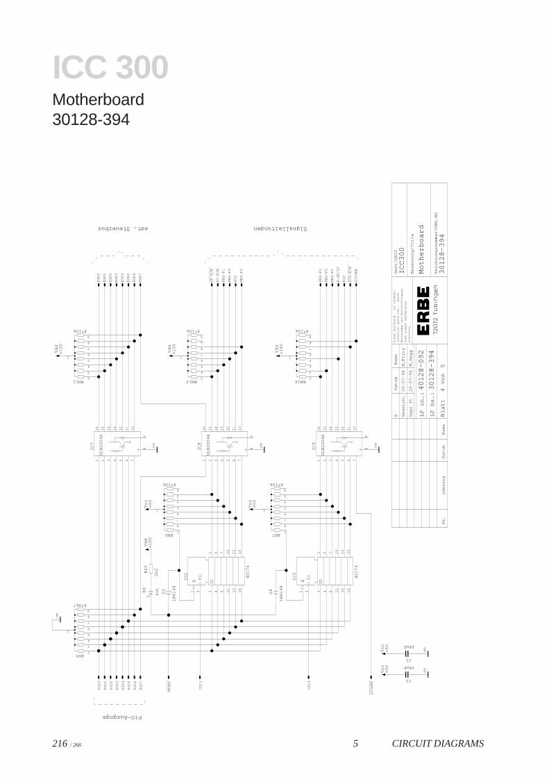
216 / 266 5 CIRCUIT DIAGRAMS
ICC 300Motherboard30128-394
PIO-Ausgnge
Signalleitungenext. Steuerbus
4
Die
se Z
eic
hn
un
gis
t u
rhe
be
r-
oh
ne
un
sere
Ge
ne
hm
igu
ng
Be
ne
nn
un
g/T
itle
Ze
ich
nu
ng
snu
mm
er/
DW
G.N
O
Ge
rt/U
NIT
We
iterg
ab
e u
nd
Ve
rvie
lfltig
un
gre
chtli
ch g
esc
htz
t,d
ah
er
un
zuls
sig
Da
tum
Na
me
Ge
zeic
h.
Ge
pr
ft
LP
un
.:
LP
bs.
:
Bla
ttvo
nD
atu
mN
am
en
de
run
gN
r.
M.F
ritz
Mo
the
rbo
ard
A
40
12
8-0
92
20
-07
-94
5
20
-07
-94
M.H
ag
g
30
12
8-3
94
30
12
8-3
94
ICC
30
0
C1
68nF
C2
68nF
D3
1N
41
48
D4
1N
41
48
rotD8
1DR C
1 40
17
4
IC2
1DR C
1 40
17
4
IC3
IC7
UL
N2
00
4A
IC8
UL
N2
00
4A
IC9
UL
N2
00
4A
R1
0
2k2
RN5
8*4k7
RN6
8*10k
RN7
8*10k
RN12
8*10k
RN13
8*10k
RN14
8*10k
HF
-EIN
RE
SE
T
SIC
HE
R
ST
E-E
IN
CS
13
CS
14
ES
D0
ES
D1
ES
D2
ES
D3
ES
D4
ES
D5
ES
D6
ES
D7
GN
D
GN
DG
ND
GN
D
GN
D
GN
D
NT
-EIN
NT
E
PS
D0
PS
D1
PS
D2
PS
D3
PS
D4
PS
D5
PS
D6
PS
D7
R-B
F/C
F
RE
L-N
T
RE
S-F
1
RE
S-F
2
RE
S-F
3
RE
S-F
4
RE
S-F
5
RL
V
SIC
HE
R
Vcc
+5
V
Vcc
+5
VV
cc+
5V
Vcc
+5
V
+1
5V
Vd
d
+1
5V
Vd
d
+1
5V
Vd
d
+1
5V
Vd
d
1 32
45
67
11
10
13
12
14
15
9 1 32
45
67
11
10
13
12
14
15
9
1 2 3 4 5 6 7
16
15
14
13
12
11
10
89
1 2 3 4 5 6 7
16
15
14
13
12
11
10
89
1 2 3 4 5 6 7
16
15
14
13
12
11
10
89
1
2
3
4
5
6
7
8
9
1
2
8
7
6
5
4
3
9
1
2
8
7
6
5
4
3
9
1
2
3
4
5
6
7
8
9
1
3
4
5
6
7
8
2
9
1
2
3
4
5
6
7
8
9
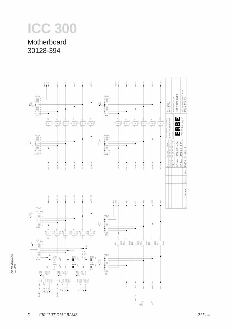
5 CIRCUIT DIAGRAMS 217 / 266
Art
. No.
801
16-2
0109
/ 20
04
ICC 300Motherboard30128-394
5
Fu
Æsc
ha
lter
1
Fu
Æsc
ha
lter
2
Die
se Z
eic
hn
un
gis
t u
rhe
be
r-
oh
ne
un
sere
Ge
ne
hm
igu
ng
Be
ne
nn
un
g/T
itle
Ze
ich
nu
ng
snu
mm
er/
DW
G.N
O
Ge
rt/U
NIT
We
iterg
ab
e u
nd
Ve
rvie
lfltig
un
gre
chtli
ch g
esc
htz
t,d
ah
er
un
zuls
sig
Da
tum
Na
me
Ge
zeic
h.
Ge
pr
ft
LP
un
.:
LP
bs.
:
Bla
ttvo
nD
atu
mN
am
en
de
run
gN
r.
M.F
ritz
Mo
the
rbo
ard
A
40
12
8-0
92
20
-07
-94
5
20
-07
-94
M.H
ag
g
30
12
8-3
94
30
12
8-3
94
ICC
30
0
C19
68nF
C18
68nF
C17
68nF
C16
68nF
C20
68nF
C21
68nF
IC5 1
40
50
IC5 1
40
50
IC5 1
40
50
IC5 1
40
50
IC5 1
40
50
IC5 1
40
50
IC1
3
40
50
1
IC1
3
40
50
1
IC1
3
40
50
1
IC1
3
40
50
1
IC1
3
40
50
1
IC1
3
40
50
1
IC6 1
40
50
IC6 1
40
50
IC6 1
40
50
IC6 1
40
50
IC6 1
40
50
IC6 1
40
50
IC1 1
40
50
IC1 1
40
50
IC1 1
40
50
IC1 1
40
50
IC1 1
40
50
IC1 1
40
50
J24
J23
J25
R1
1
68
0R
R1
7
68
0R
R1
6
68
0R
R1
2
68
0R
R1
5
68
0R
R1
4
68
0R
R1
3
68
0R
R1
8
68
0R
R1
9
68
0R
R20
0R
RN10
8*10k
RN3
8*10k
RN18
8*2k2
RN17
8*10k
RN11
8*10k
RN4
8*10k
RN2
8*10k
RN1
8*10k
BF
/CF
BF
/CF
EIN
1
EIN
10
EIN
11
EIN
12
EIN
13
EIN
14
EIN
15
EIN
16
EIN
17
EIN
18
EIN
19
EIN
2
EIN
20
EIN
21
EIN
22
EIN
23
EIN
3
EIN
4
EIN
5
EIN
6
EIN
7
EIN
8
EIN
9
F-S
T
FIN
G-A
1
FIN
G-A
2
FIN
G-A
3
FIN
G-B
1
FIN
G-B
2
FIN
G-B
3
FU
FI-
A3
FU
FI-
A3
FU
FI-
B3
FU
FI-
B3
FU
SS
-A1
FU
SS
-A1
FU
SS
-A2
FU
SS
-A2
FU
SS
-B1
FU
SS
-B1
FU
SS
-B2
FU
SS
-B2
GN
D
GN
D
GN
D
GN
DG
ND
GN
DG
ND
GN
DG
ND
GN
D
RE
S-B
1
RE
S-B
2
RE
S-B
3
RE
S-B
5
RE
S-B
6
Vcc
+5
V
Vcc
+5
VV
cc+
5V
+1
5V
Vd
d
+1
5V
Vd
d
+1
5V
Vd
d
+1
5V
Vd
d
+1
5V
Vd
d
14
15
32
54
11
12
76
91
0
32
14
15
11
12
54
76
91
0
14
15
32
54
11
12
76
91
0
14
15
54
11
12
76
91
0
32
1 2 31 2 3 1 2 3
1
2
3
4
5
6
7
8
9
1
2
3
4
5
6
7
8
9
1
5
3
7
6
8
9
4
2
1
2
3
5
4
6
7
8
9
1
2
3
4
5
6
7
8
9
1
2
3
4
5
6
7
8
9
1
9
7
3
5
8
6
2
4
1
3
4
5
7
9
2
8
6
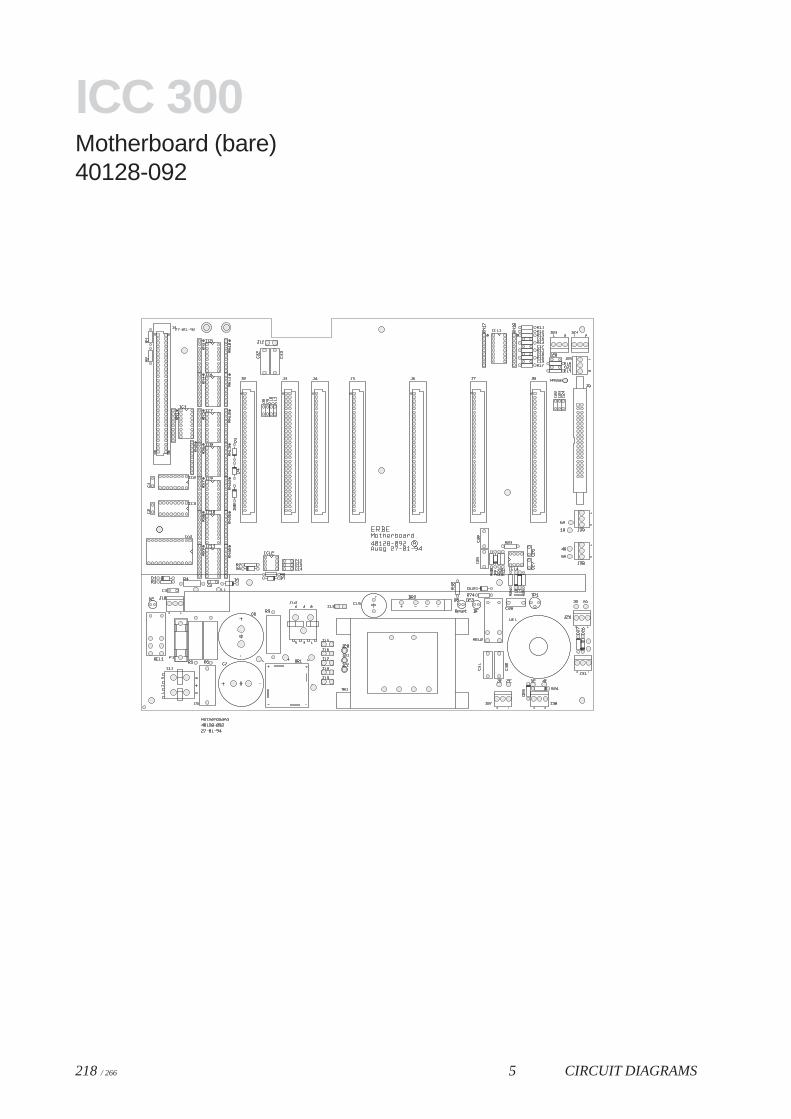
218 / 266 5 CIRCUIT DIAGRAMS
ICC 300Motherboard (bare)40128-092
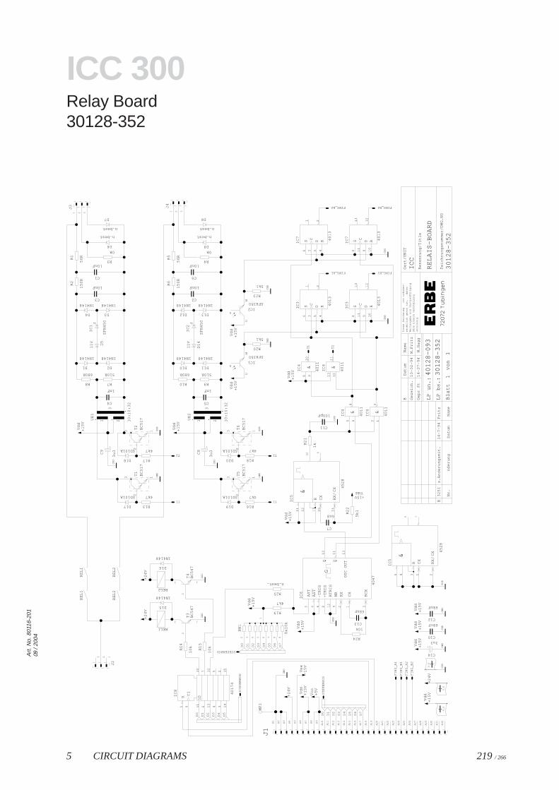
5 CIRCUIT DIAGRAMS 219 / 266
Art
. No.
801
16-2
0109
/ 20
04
ICC 300Relay Board30128-352
Die
se Z
eic
hn
un
gis
t u
rhe
be
r-
oh
ne
un
sere
Ge
ne
hm
igu
ng
Be
ne
nn
un
g/T
itle
Ze
ich
nu
ng
snu
mm
er/
DW
G.N
O
Ge
rt/U
NIT
We
iterg
ab
e u
nd
Ve
rvie
lfltig
un
gre
chtli
ch g
esc
htz
t,d
ah
er
un
zuls
sig
Da
tum
Na
me
Ge
zeic
h.
Ge
pr
ft
LP
un
.:
LP
bs.
:
Bla
ttvo
nD
atu
mN
am
en
de
run
g
40
12
8-0
93
30
12
8-3
52
30
12
8-3
52
ICC
RE
LA
IS-B
OA
RD
11
10
-02
-94
B
32
51
Nr.
Fritz
14
-7-9
4s.
An
de
run
gsm
it.B
M.H
ag
g
M.F
ritz
14
-07
-94
0.6
0.6
0.8
C14
+
3u3
C4
1nF
C3
10nF
C1
10nF
C5
1nF
C2
10nF
C6
10nF
C13
68nF
C7
6n8
C10
68nF
C12
68nF
C9
+
3u
3 C8
+
3u
3
C11
100pF
D6
n.best
D15
1N4148
D16
1N4148
D1
1N4148
D2
1N4148
D4
1N4148
D3
1N4148
D18
SD101A
D17
SD101A
D10
1N4148
D11
1N4148
D7
n.best
D12
1N4148
D13
1N4148
D20
SD101A
D19
SD101A
D5
11
V
D9
n.best
D8
n.best
D1
4
11
V
1DR C
1 40
17
4
IC8
SFH350
IC1
IC1
SF
H4
50
IC2
SF
H4
50
SFH350
IC2
40
47
RC
X
CX
Q Q
IC6 AS
T
-TR
IG
+T
RIG
RT
RIG
MR
RX
AS
T
OS
C O
UT
G
IC5 CX
R
&
RX
/CX 4
52
8
IC5 CX
R
&
RX
/CX 4
52
8
&
IC4
40
11
&
IC4
40
11
&
IC4
40
11
&
IC4
40
11
S RIC3
D 40
13
C S RIC3
D 40
13
C
S RIC7
D 40
13
C S RIC7
D 40
13
C
J2
J3 J4
J1M
P1
R1
5
10
kR1
4
10
k
R13
4k7
R17
4k7
R7
510R
R8
680R
R2
15
0R
R1
56
R
R3
0R
R20
5k1
R16
4k7
R18
4k7
R9
510R
R10
680R
R6
15
0R
R5
56
R
R4
0R
R23
5k1
R24
10k
R2
2
5k1
R19
4k7
R25
n.best.
R2
1
1k
RE
L1
RE
L1
RE
L2
RE
L2
REL1
REL2
RN
1
8x1
0k
T3
BC
54
7T
4B
C5
47
T1
BC
51
7
T2
BC
51
7
T5
BC
51
7
T6
BC
51
7UE
1
10
:10
:32
1 2
3
UE
2
10
:10
:32
1 2
3
FIN
G_
A1
FING_A1
FIN
G_
A2
FING_A2
FIN
G_
B1
FING_B1
FIN
G_
B2
FING_B2
GN
D
GN
D
GN
D
GN
D
GN
DG
ND
GN
D
GN
DG
ND
GN
D
GN
D
GN
DG
ND
GN
D
GN
DG
ND
GN
DG
ND
GN
DG
ND
+2
4V
+2
4V
+2
4V
+2
4V
ST
EU
ER
BU
S
ST
EU
ER
BU
S
STEUERBUS
T1T1
T1
T2 T2T
2
Vcc
+5
V
+1
5V
Vd
d
+1
5V
Vd
d+
15
VV
dd
+1
5V
Vd
d
+1
5V
Vd
d
+1
5V
Vd
d
+1
5V
Vd
d
+1
5V
Vd
d
+1
5V
Vd
d
+1
5V
Vd
d
+1
5V
Vd
d
+1
5V
Vd
d+
15
VV
dd
+15VVdd
Ve
e-1
5V
D5
D4
D3
D2
D1
D0 D7
D6
D5
D4
D3
D2
D1
D0
D7
D6
D5
D4
D3
D2
D1
D0
1 11
10
67
13
12
45
32
14
15
9
B
C
E
B
C
E
864
11
5 19
13
10
312
2
13
9
11
12
15
10
14
37
5 4 1
6
2
5 64
2 13
8 91
0
13
12
11
2
3 4561 1
2
11
10
981
3
2
3 4561 1
2
11
10
981
3
123
1 2 3 1 2 3
A1
A1
0
A1
1
A1
2
A1
3
A1
4
A1
5
A1
6
A1
7
A1
8
A1
9
A2
A2
0
A2
1
A2
2
A2
3
A2
4
A2
5
A2
6
A2
7
A2
8
A2
9
A3
A3
0
A3
1
A3
2
A4
A5
A6
A7
A8
A9
1
2 3 4 5 6 7 8 9
2
3 1
2
3 1
2
3 1
2
3 1
2
3 1
2
3 1
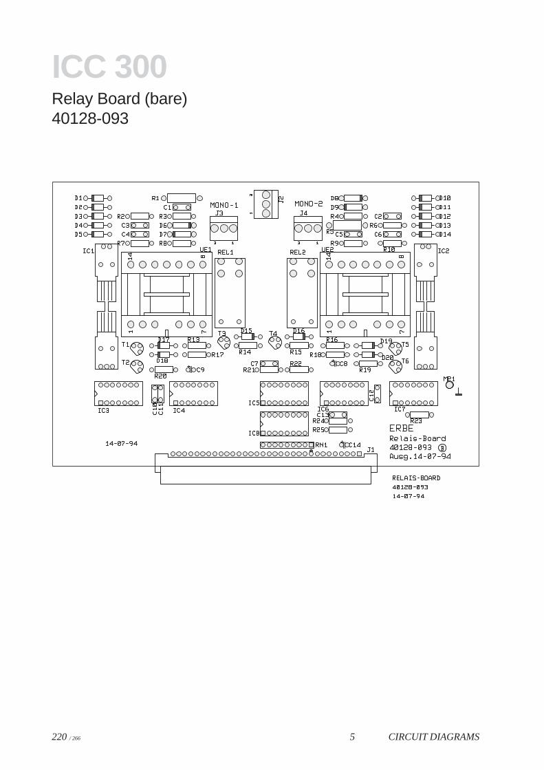
220 / 266 5 CIRCUIT DIAGRAMS
ICC 300Relay Board (bare)40128-093

PCBsonly for ICC 350

222 / 266 5 CIRCUIT DIAGRAMS
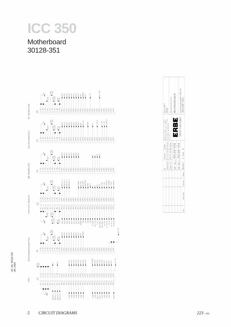
5 CIRCUIT DIAGRAMS 223 / 266
Art
. No.
801
16-2
0109
/ 20
04
ICC 350Motherboard30128-351
1
CP
UK
lein
spa
nn
un
g+
To
nS
T-E
nd
stu
feL
eis
tun
gst
eil
QK
-En
dst
ufe
Co
ntr
ol-B
oa
rd
Die
se Z
eic
hn
un
gis
t u
rhe
be
r-
oh
ne
un
sere
Ge
ne
hm
igu
ng
Be
ne
nn
un
g/T
itle
Ze
ich
nu
ng
snu
mm
er/
DW
G.N
O
Ge
rt/U
NIT
We
iterg
ab
e u
nd
Ve
rvie
lfltig
un
gre
chtli
ch g
esc
htz
t,d
ah
er
un
zuls
sig
Da
tum
Na
me
Ge
zeic
h.
Ge
pr
ft
LP
un
.:
LP
bs.
:
Bla
ttvo
nD
atu
mN
am
en
de
run
gN
r.
M.F
ritz
ICC
6
Mo
the
rbo
ard
A
27
.01
.94
40
12
8-0
92
30
12
8-3
51
30
12
8-3
51
20
-07
-94
M.H
ag
g
J1J2
J3J4
J5J6
CS
1
CS
2
CS
3
CS
4
CS
5
CS
6
CS
7
HF
-EIN
RE
SE
T
RE
SE
T
RE
SE
T
SIC
HE
R
ST
E-E
IN
24
V-T
R
24
V-T
R
AA
AN
AN
AN
AL
OG
-1
AN
AL
OG
-1
AN
AL
OG
-2
AN
AL
OG
-2
AN
AL
OG
-3
AN
AL
OG
-3
AN
AL
OG
-4
AN
AL
OG
-4
AU
SA
US
BB
CS
EIN
1
EIN
10
EIN
11
EIN
12
EIN
13
EIN
14
EIN
15
EIN
16
EIN
17
EIN
18
EIN
19
EIN
2
EIN
20
EIN
21
EIN
22
EIN
23
EIN
3
EIN
4
EIN
5
EIN
6
EIN
7
EIN
8
EIN
9
ES
D0
ES
D0
ES
D0
ES
D0
ES
D0
ES
D1
ES
D1
ES
D1
ES
D1
ES
D1
ES
D2
ES
D2
ES
D2
ES
D2
ES
D2
ES
D3
ES
D3
ES
D3
ES
D3
ES
D3
ES
D4
ES
D4
ES
D4
ES
D4
ES
D4
ES
D5
ES
D5
ES
D5
ES
D5
ES
D5
ES
D6
ES
D6
ES
D6
ES
D6
ES
D6
ES
D7
ES
D7
ES
D7
ES
D7
ES
D7
F-S
T
GN
D
GN
DG
ND
GN
DG
ND
GN
DG
ND
I-H
FL
IP-P
AT
IP-P
AT
-A
NT
-EIN
NT
E
+2
4V
+2
4V
+2
4V
+2
4V
+2
4V
+2
4V
PS
D0
PS
D1
PS
D2
PS
D3
PS
D4
PS
D5
PS
D6
PS
D7
RE
L-N
T
RE
S-A
NA
1
RE
S-A
NA
2
RE
SE
T
SE
T
SIC
HE
R
TE
MP
TE
MP
TS
I
TS
I
TS
I-S
TE
TS
I-S
TE
U-F
UN
KE
U-I
NP
U-I
NP
U-I
NT
U-I
NT
U-N
ES
SY
U-N
ET
ZT
U-N
ET
ZT
U-P
HA
SE
U-P
RIM
U-P
RIM
U-S
YM
UP
-HF
UP
-HF
-A
Vcc
+5
V
Vcc
+5
VV
cc+
5V
Vcc
+5
VV
cc+
5V
Vcc
+5
VV
cc+
5V
+1
5V
Vd
d+
15
VV
dd
+1
5V
Vd
d+
15
VV
dd
+1
5V
Vd
d+
15
VV
dd
Ve
e-1
5V
Ve
e-1
5V
Ve
e-1
5V
Ve
e-1
5V
Ve
e-1
5V
Ve
e-1
5V
A1
A1
0
A1
1
A1
2
A1
3
A1
4
A1
5
A1
6
A1
7
A1
8
A1
9
A2
A2
0
A2
1
A2
2
A2
3
A2
4
A2
5
A2
6
A2
7
A2
8
A2
9
A3
A3
0
A3
1
A3
2
A4
A5
A6
A7
A8
A9
C1
C1
0
C1
1
C1
2
C1
3
C1
4
C1
5
C1
6
C1
7
C1
8
C1
9
C2
C2
0
C2
1
C2
2
C2
3
C2
4
C2
5
C2
6
C2
7
C2
8
C2
9
C3
C3
0
C3
1
C3
2
C4
C5
C6
C7
C8
C9
A1
A1
0
A1
1
A1
2
A1
3
A1
4
A1
5
A1
6
A1
7
A1
8
A1
9
A2
A2
0
A2
1
A2
2
A2
3
A2
4
A2
5
A2
6
A2
7
A2
8
A2
9
A3
A3
0
A3
1
A3
2
A4
A5
A6
A7
A8
A9
A1
A1
0
A1
1
A1
2
A1
3
A1
4
A1
5
A1
6
A1
7
A1
8
A1
9
A2
A2
0
A2
1
A2
2
A2
3
A2
4
A2
5
A2
6
A2
7
A2
8
A2
9
A3
A3
0
A3
1
A3
2
A4
A5
A6
A7
A8
A9
B1
B1
0
B1
1
B1
2
B1
3
B1
4
B1
5
B1
6
B1
7
B1
8
B1
9
B2
B2
0
B2
1
B2
2
B2
3
B2
4
B2
5
B2
6
B2
7
B2
8
B2
9
B3
B3
0
B3
1
B3
2
B4
B5
B6
B7
B8
B9
A1
A1
0
A1
1
A1
2
A1
3
A1
4
A1
5
A1
6
A1
7
A1
8
A1
9
A2
A2
0
A2
1
A2
2
A2
3
A2
4
A2
5
A2
6
A2
7
A2
8
A2
9
A3
A3
0
A3
1
A3
2
A4
A5
A6
A7
A8
A9
A1
A1
0
A1
1
A1
2
A1
3
A1
4
A1
5
A1
6
A1
7
A1
8
A1
9
A2
A2
0
A2
1
A2
2
A2
3
A2
4
A2
5
A2
6
A2
7
A2
8
A2
9
A3
A3
0
A3
1
A3
2
A4
A5
A6
A7
A8
A9
A1
A1
0
A1
1
A1
2
A1
3
A1
4
A1
5
A1
6
A1
7
A1
8
A1
9
A2
A2
0
A2
1
A2
2
A2
3
A2
4
A2
5
A2
6
A2
7
A2
8
A2
9
A3
A3
0
A3
1
A3
2
A4
A5
A6
A7
A8
A9
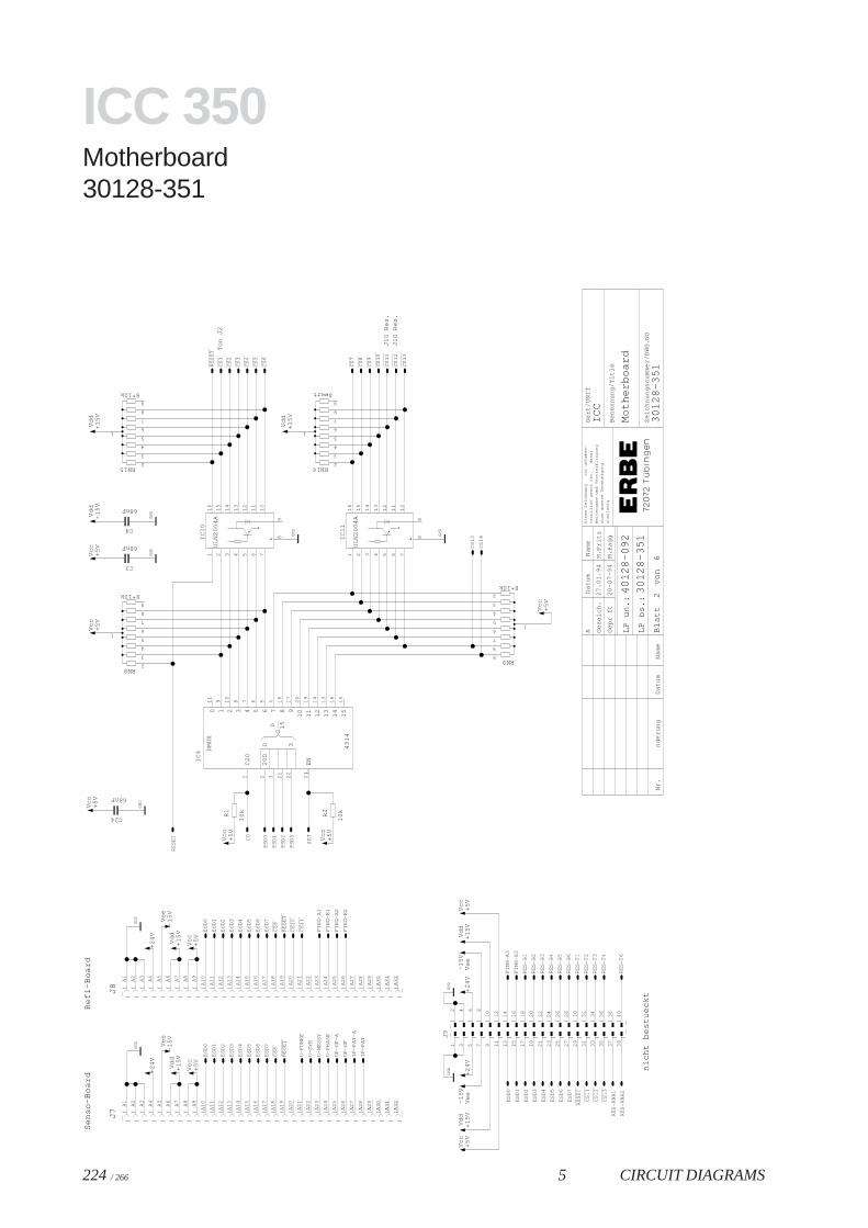
224 / 266 5 CIRCUIT DIAGRAMS
ICC 350Motherboard30128-351
2
To
n J
2
J10
Re
s.
J10
Re
s.
Se
nso
-Bo
ard
Re
fi-B
oa
rd
nic
ht b
est
ue
ckt
Die
se Z
eic
hn
un
gis
t u
rhe
be
r-
oh
ne
un
sere
Ge
ne
hm
igu
ng
Be
ne
nn
un
g/T
itle
Ze
ich
nu
ng
snu
mm
er/
DW
G.N
O
Ge
rt/U
NIT
We
iterg
ab
e u
nd
Ve
rvie
lfltig
un
gre
chtli
ch g
esc
htz
t,d
ah
er
un
zuls
sig
Da
tum
Na
me
Ge
zeic
h.
Ge
pr
ft
LP
un
.:
LP
bs.
:
Bla
ttvo
nD
atu
mN
am
en
de
run
gN
r.
M.F
ritz
ICC
6
Mo
the
rbo
ard
A
27
.01
.94
40
12
8-0
92
30
12
8-3
51
30
12
8-3
51
20
-07
-94
M.H
ag
g
C3
68nF
C4
68nF
C24
68nF
0 1 2 3
DM
UX
4 65 7 8 9
10
11
12
13
14
15
20
D0 3
G1
50
C2
0
ENIC
4
45
14
IC1
0
UL
N2
00
4A
IC1
1
UL
N2
00
4A
J9
J7J8
R1
10
k R2
10
k
RN8
8*10k
RN9
8*10k
RN15
8*10k
RN16
$wert
CS
1
CS
10
CS
10
CS
11
CS
11
CS
11
CS
12
CS
12
CS
13
CS
13
CS
2
CS
3
CS
4
CS
5
CS
6
CS
7
CS
8
CS
8
CS
9
CS
9
RE
SE
T
RE
SE
T
RE
SE
T
RE
SE
T
CS
CS
13
CS
14
ES
D0
ES
D0
ES
D0
ES
D1
ES
D1
ES
D1
ES
D2
ES
D2
ES
D2
ES
D3
ES
D3
ES
D3
ES
D4
ES
D4
ES
D4
ES
D5
ES
D5
ES
D5
ES
D6
ES
D6
ES
D6
ES
D7
ES
D7
ES
D7
FIN
G-A
1
FIN
G-A
2
FIN
G-A
3
FIN
G-B
1
FIN
G-B
2
FIN
G-B
3
GN
D
GN
DG
ND
GN
D
GN
DG
ND
GN
D
GN
D
GN
D
IP-P
AT
IP-P
AT
-A
+2
4V
+2
4V
+2
4V
+2
4V
PS
D0
PS
D1
PS
D2
PS
D3
RE
S-A
NA
1
RE
S-A
NA
2
RE
S-B
1
RE
S-B
2
RE
S-B
3
RE
S-B
4
RE
S-B
5
RE
S-B
6
RE
S-F
1
RE
S-F
2
RE
S-F
3
RE
S-F
4
RE
S-F
6
RE
SE
T
SE
T
U-F
UN
KE
U-N
ES
SY
U-P
HA
SE
U-S
YM
UP
-HF
UP
-HF
-A
Vcc
+5
V
Vcc
+5
VV
cc+
5V
Vcc
+5
V
Vcc
+5
V
Vcc
+5
VV
cc+
5V
Vcc
+5
V
Vcc
+5
V
Vcc
+5
V
+1
5V
Vd
d
+1
5V
Vd
d+
15
VV
dd
+1
5V
Vd
d
+1
5V
Vd
d+
15
VV
dd
+1
5V
Vd
d
Ve
e-1
5V
Ve
e-1
5V
Ve
e-1
5V
Ve
e-1
5V
23
2 3 21
22
1
11
9 20
19
14
13
16
15
10
8 7 6 5 4 18
17
1 2 3 4 5 6 7
16
15
14
13
12
11
10
89
1 2 3 4 5 6 7
16
15
14
13
12
11
10
89
1
10
11
12
13
14
15
16
17
18
19
2
20
21
22
23
24
25
26
27
28
29
3
30
31
32
33
34
35
36
37
38
39
4
40
56
78
9
A1
A1
0
A1
1
A1
2
A1
3
A1
4
A1
5
A1
6
A1
7
A1
8
A1
9
A2
A2
0
A2
1
A2
2
A2
3
A2
4
A2
5
A2
6
A2
7
A2
8
A2
9
A3
A3
0
A3
1
A3
2
A4
A5
A6
A7
A8
A9
A1
A1
0
A1
1
A1
2
A1
3
A1
4
A1
5
A1
6
A1
7
A1
8
A1
9
A2
A2
0
A2
1
A2
2
A2
3
A2
4
A2
5
A2
6
A2
7
A2
8
A2
9
A3
A3
0
A3
1
A3
2
A4
A5
A6
A7
A8
A9
1
2
3
4
5
6
7
8
9
1
8
9
7
6
5
4
3
2
1
2
3
4
5
6
7
8
9
1
2
3
4
5
6
7
8
9

5 CIRCUIT DIAGRAMS 225 / 266
Art
. No.
801
16-2
0109
/ 20
04
ICC 350Motherboard30128-351
3
Ge
hu
se
Le
istu
ng
ste
il
Fro
ntp
latte
Die
se Z
eic
hn
un
gis
t u
rhe
be
r-
oh
ne
un
sere
Ge
ne
hm
igu
ng
Be
ne
nn
un
g/T
itle
Ze
ich
nu
ng
snu
mm
er/
DW
G.N
O
Ge
rt/U
NIT
We
iterg
ab
e u
nd
Ve
rvie
lfltig
un
gre
chtli
ch g
esc
htz
t,d
ah
er
un
zuls
sig
Da
tum
Na
me
Ge
zeic
h.
Ge
pr
ft
LP
un
.:
LP
bs.
:
Bla
ttvo
nD
atu
mN
am
en
de
run
gN
r.
M.F
ritz
ICC
6
Mo
the
rbo
ard
A
27
.01
.94
40
12
8-0
92
30
12
8-3
51
30
12
8-3
51
20
-07
-94
M.H
ag
g
0.5
0.5
0.5
+-
~ ~
BR
1
BH
37
93
3
+-
~ ~B
R2
B2
50
C5
00
0
C6
+
680uF
C7
+
680uF
C15
+
1000uF
C5
u68
C11
68nF
C22
68nF
C9
68nF
C23
68nF
C8
68nF
C10
68nF
C32
u022
C33
u022
D1
1N
41
48
rotD2
F1
T2
00
mA
J12
J10
J11
J14
J15
J16
J19
J18
J17
J20
J22
J21
J13
MA
SS
E
R5
10
0R
R6
22k
R9
22k
R3
3k6
RE
L1
RE
L1
RE
L1
TR
1
24
V
Prim.1 Prim.2
Sek.
24
V-T
R
GN
D
GN
DG
ND
GN
DG
ND
GN
DG
ND
GN
D
GN
D
+2
4V
+2
4V
RL
V
Vcc
+5
V
Vcc
+5
V
+1
5V
Vd
d
+1
5V
Vd
d
Ve
e-1
5V
1
1 2 3
1 2 5 6
2361
1
1 1 1
1
1 1
1
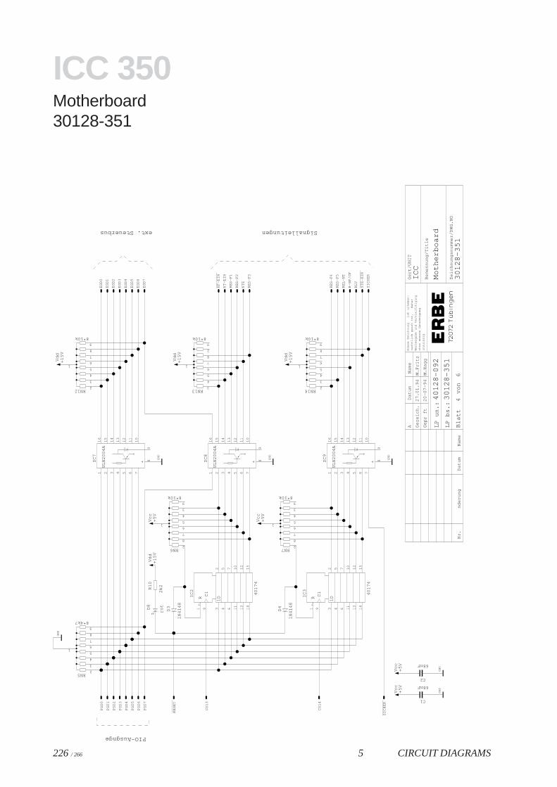
226 / 266 5 CIRCUIT DIAGRAMS
ICC 350Motherboard30128-351
PIO-Ausgnge
Signalleitungenext. Steuerbus
4
Die
se Z
eic
hn
un
gis
t u
rhe
be
r-
oh
ne
un
sere
Ge
ne
hm
igu
ng
Be
ne
nn
un
g/T
itle
Ze
ich
nu
ng
snu
mm
er/
DW
G.N
O
Ge
rt/U
NIT
We
iterg
ab
e u
nd
Ve
rvie
lfltig
un
gre
chtli
ch g
esc
htz
t,d
ah
er
un
zuls
sig
Da
tum
Na
me
Ge
zeic
h.
Ge
pr
ft
LP
un
.:
LP
bs.
:
Bla
ttvo
nD
atu
mN
am
en
de
run
gN
r.
M.F
ritz
ICC
6
Mo
the
rbo
ard
A
27
.01
.94
40
12
8-0
92
30
12
8-3
51
30
12
8-3
51
20
-07
-94
M.H
ag
g
C1
68nF
C2
68nF
D3
1N
41
48
D4
1N
41
48
rotD8
1DR C
1 40
17
4
IC2
1DR C
1 40
17
4
IC3
IC7
UL
N2
00
4A
IC8
UL
N2
00
4A
IC9
UL
N2
00
4A
R1
0
2k2
RN5
8*4k7
RN6
8*10k
RN7
8*10k
RN12
8*10k
RN13
8*10k
RN14
8*10k
HF
-EIN
RE
SE
T
SIC
HE
R
ST
E-E
IN
CS
13
CS
14
ES
D0
ES
D1
ES
D2
ES
D3
ES
D4
ES
D5
ES
D6
ES
D7
GN
D
GN
DG
ND
GN
D
GN
D
GN
D
NT
-EIN
NT
E
PS
D0
PS
D1
PS
D2
PS
D3
PS
D4
PS
D5
PS
D6
PS
D7
R-B
F/C
F
RE
L-N
T
RE
S-F
1
RE
S-F
2
RE
S-F
3
RE
S-F
4
RE
S-F
5
RL
V
SIC
HE
R
Vcc
+5
V
Vcc
+5
VV
cc+
5V
Vcc
+5
V
+1
5V
Vd
d
+1
5V
Vd
d
+1
5V
Vd
d
+1
5V
Vd
d
1 32
45
67
11
10
13
12
14
15
9 1 32
45
67
11
10
13
12
14
15
9
1 2 3 4 5 6 7
16
15
14
13
12
11
10
89
1 2 3 4 5 6 7
16
15
14
13
12
11
10
89
1 2 3 4 5 6 7
16
15
14
13
12
11
10
89
1
2
3
4
5
6
7
8
9
1
2
8
7
6
5
4
3
9
1
2
8
7
6
5
4
3
9
1
2
3
4
5
6
7
8
9
1
3
4
5
6
7
8
2
9
1
2
3
4
5
6
7
8
9
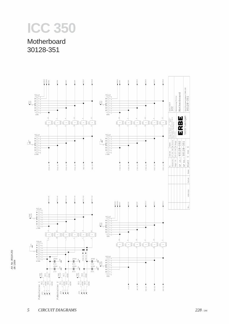
5 CIRCUIT DIAGRAMS 228 / 266
Art
. No.
801
16-2
0109
/ 20
04
ICC 350Motherboard30128-351
5
Fu
Æsc
ha
lter
1
Fu
Æsc
ha
lter
2
Die
se Z
eic
hn
un
gis
t u
rhe
be
r-
oh
ne
un
sere
Ge
ne
hm
igu
ng
Be
ne
nn
un
g/T
itle
Ze
ich
nu
ng
snu
mm
er/
DW
G.N
O
Ge
rt/U
NIT
We
iterg
ab
e u
nd
Ve
rvie
lfltig
un
gre
chtli
ch g
esc
htz
t,d
ah
er
un
zuls
sig
Da
tum
Na
me
Ge
zeic
h.
Ge
pr
ft
LP
un
.:
LP
bs.
:
Bla
ttvo
nD
atu
mN
am
en
de
run
gN
r.
M.F
ritz
ICC
6
Mo
the
rbo
ard
A
27
.01
.94
40
12
8-0
92
30
12
8-3
51
30
12
8-3
51
20
-07
-94
M.H
ag
g
C19
68nF
C18
68nF
C17
68nF
C16
68nF
C20
68nF
C21
68nF
IC5 1
40
50
IC5 1
40
50
IC5 1
40
50
IC5 1
40
50
IC5 1
40
50
IC5 1
40
50
IC1
3
40
50
1
IC1
3
40
50
1
IC1
3
40
50
1
IC1
3
40
50
1
IC1
3
40
50
1
IC1
3
40
50
1
IC6 1
40
50
IC6 1
40
50
IC6 1
40
50
IC6 1
40
50
IC6 1
40
50
IC6 1
40
50
IC1 1
40
50
IC1 1
40
50
IC1 1
40
50
IC1 1
40
50
IC1 1
40
50
IC1 1
40
50
J24
J23
J25
R1
1
68
0R
R1
7
68
0R
R1
6
68
0R
R1
2
68
0R
R1
5
68
0R
R1
4
68
0R
R1
3
68
0R
R1
8
68
0R
R1
9
68
0R
RN10
8*10k
RN3
8*10k
RN18
8*2k2
RN17
8*10k
RN11
8*10k
RN4
8*10k
RN2
8*10k
RN1
8*10k
BF
/CF
EIN
1
EIN
10
EIN
11
EIN
12
EIN
13
EIN
14
EIN
15
EIN
16
EIN
17
EIN
18
EIN
19
EIN
2
EIN
20
EIN
21
EIN
22
EIN
23
EIN
3
EIN
4
EIN
5
EIN
6
EIN
7
EIN
8
EIN
9
F-S
T
FIN
G-A
1
FIN
G-A
2
FIN
G-A
3
FIN
G-B
1
FIN
G-B
2
FIN
G-B
3
FU
FI-
A3
FU
FI-
A3
FU
FI-
B3
FU
FI-
B3
FU
SS
-A1
FU
SS
-A1
FU
SS
-A2
FU
SS
-A2
FU
SS
-B1
FU
SS
-B1
FU
SS
-B2
FU
SS
-B2
GN
D
GN
D
GN
DG
ND
GN
DG
ND
GN
DG
ND
GN
D
RE
S-B
1
RE
S-B
2
RE
S-B
3
RE
S-B
5
RE
S-B
6
Vcc
+5
V
Vcc
+5
VV
cc+
5V
+1
5V
Vd
d
+1
5V
Vd
d
+1
5V
Vd
d
+1
5V
Vd
d
+1
5V
Vd
d
14
15
32
54
11
12
76
91
0
32
14
15
11
12
54
76
91
0
14
15
32
54
11
12
76
91
0
14
15
54
11
12
76
91
0
32
1 2 31 2 3 1 2 3
1
2
3
4
5
6
7
8
9
1
2
3
4
5
6
7
8
9
1
5
3
7
6
8
9
4
2
1
2
3
5
4
6
7
8
9
1
2
3
4
5
6
7
8
9
1
2
3
4
5
6
7
8
9
1
9
7
3
5
8
6
2
4
1
3
4
5
7
9
2
8
6
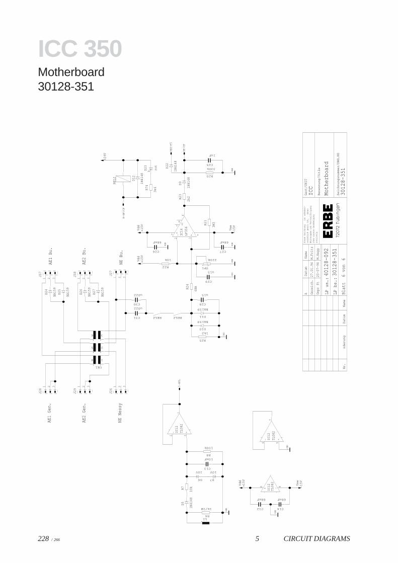
228 / 266 5 CIRCUIT DIAGRAMS
ICC 350Motherboard30128-351
6
NE B
u.NE
Nes
sy
AE1
Bu.
AE2
Bu.
AE1
Gen.
AE2
Gen.
Diese Zeichnung
ist urheber-
ohne unsere Genehmigung
Benennung/Title
Zeichnungsnummer/DWG.NO
Gert/UNIT
Weitergabe und Vervielfltigung
rechtlich geschtzt,
daher
unzulssig
Datum
Name
Gezeich.
Gepr
ft
LP u
n.:
LP b
s.:
Blat
tvo
nDatum
Name
nderung
Nr.
M.Fritz
ICC
6
Motherboard
A
27.01.94
40128-092
30128-351
30128-351
20-07-94
M.Hagg
C13
10nF
C12
68nF
C14
68nF
C28
u15
C31
u022
C30
u022
C29
u15
C26
68nF
C27
68nF
C25
1uF
D5
1N4148
D6
10V
D7
10V
D10
BA159
D11
BA159
D12
1N4148
D9
1N4148
D22
1N4148
rot
D23
D24
BA159
D25
BA159
D26
BA159
D27
BA159
IC12
+- TL082
IC12
+- TL082
-+
IC12
TL082
IC14
+-+
-OF
F
LF356
J26
J27
J28
J29
J57
J58
L1R4
1k/1W
R7
10k
R8
100k
R25
1k2
R24
68R
R22
10k
R21
3M3
R23
2k2
R20
330k
R74
3k6
REL2 REL2
REL2
TP1
220R
UE1
1
2
3
4
5
6
BF/C
F
GND
GND
GND
GND
GND
GND
GND
GND
GND
I-HF
L
+24V
R-BF
/CF
RES-
F5
+15V
Vdd
+15V
Vdd
+15V
Vdd
Vee
-15V
Vee
-15V
2 3
1
6 5
7
48
2
1
5
3
4
6
7
1 2 3
1 2 3
1 2 3 1 2 3
1 2 3 1 2 3
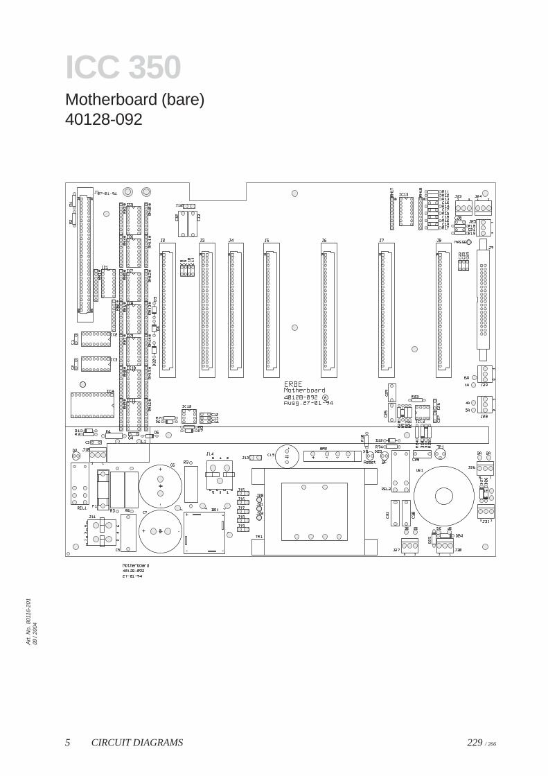
5 CIRCUIT DIAGRAMS 229 / 266
Art
. No.
801
16-2
0109
/ 20
04
ICC 350Motherboard (bare)40128-092
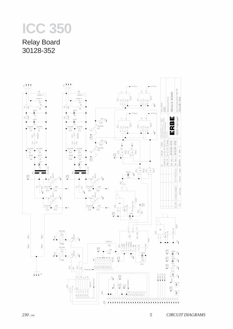
230 / 266 5 CIRCUIT DIAGRAMS
ICC 350Relay Board30128-352
Die
se Z
eic
hn
un
gis
t u
rhe
be
r-
oh
ne
un
sere
Ge
ne
hm
igu
ng
Be
ne
nn
un
g/T
itle
Ze
ich
nu
ng
snu
mm
er/
DW
G.N
O
Ge
rt/U
NIT
We
iterg
ab
e u
nd
Ve
rvie
lfltig
un
gre
chtli
ch g
esc
htz
t,d
ah
er
un
zuls
sig
Da
tum
Na
me
Ge
zeic
h.
Ge
pr
ft
LP
un
.:
LP
bs.
:
Bla
ttvo
nD
atu
mN
am
en
de
run
g
40
12
8-0
93
30
12
8-3
52
30
12
8-3
52
ICC
RE
LA
IS-B
OA
RD
11
10
-02
-94
B
32
51
Nr.
Fritz
14
-7-9
4s.
An
de
run
gsm
it.B
M.H
ag
g
M.F
ritz
14
-07
-94
0.6
0.6
0.8
C14
+
3u3
C4
1nF
C3
10nF
C1
10nF
C5
1nF
C2
10nF
C6
10nF
C13
68nF
C7
6n8
C10
68nF
C12
68nF
C9
+
3u
3 C8
+
3u
3
C11
100pF
D6
n.best
D15
1N4148
D16
1N4148
D1
1N4148
D2
1N4148
D4
1N4148
D3
1N4148
D18
SD101A
D17
SD101A
D10
1N4148
D11
1N4148
D7
n.best
D12
1N4148
D13
1N4148
D20
SD101A
D19
SD101A
D5
11
V
D9
n.best
D8
n.best
D1
4
11
V
1DR C
1 40
17
4
IC8
SFH350
IC1
IC1
SF
H4
50
IC2
SF
H4
50
SFH350
IC2
40
47
RC
X
CX
Q Q
IC6 AS
T
-TR
IG
+T
RIG
RT
RIG
MR
RX
AS
T
OS
C O
UT
G
IC5 CX
R
&
RX
/CX 4
52
8
IC5 CX
R
&
RX
/CX 4
52
8
&
IC4
40
11
&
IC4
40
11
&
IC4
40
11
&
IC4
40
11
S RIC3
D 40
13
C S RIC3
D 40
13
C
S RIC7
D 40
13
C S RIC7
D 40
13
C
J2
J3 J4
J1M
P1
R1
5
10
kR1
4
10
k
R13
4k7
R17
4k7
R7
510R
R8
680R
R2
15
0R
R1
56
R
R3
0R
R20
5k1
R16
4k7
R18
4k7
R9
510R
R10
680R
R6
15
0R
R5
56
R
R4
0R
R23
5k1
R24
10k
R2
2
5k1
R19
4k7
R25
n.best.
R2
1
1k
RE
L1
RE
L1
RE
L2
RE
L2
REL1
REL2
RN
1
8x1
0k
T3
BC
54
7T
4B
C5
47
T1
BC
51
7
T2
BC
51
7
T5
BC
51
7
T6
BC
51
7UE
1
10
:10
:32
1 2
3
UE
2
10
:10
:32
1 2
3
FIN
G_
A1
FING_A1
FIN
G_
A2
FING_A2
FIN
G_
B1
FING_B1
FIN
G_
B2
FING_B2
GN
D
GN
D
GN
D
GN
D
GN
DG
ND
GN
D
GN
DG
ND
GN
D
GN
D
GN
DG
ND
GN
D
GN
DG
ND
GN
DG
ND
GN
DG
ND
+2
4V
+2
4V
+2
4V
+2
4V
ST
EU
ER
BU
S
ST
EU
ER
BU
S
STEUERBUS
T1T1T
1
T2 T2
T2
Vcc
+5
V
+1
5V
Vd
d
+1
5V
Vd
d+
15
VV
dd
+1
5V
Vd
d
+1
5V
Vd
d
+1
5V
Vd
d
+1
5V
Vd
d
+1
5V
Vd
d
+1
5V
Vd
d
+1
5V
Vd
d
+1
5V
Vd
d
+1
5V
Vd
d+
15
VV
dd
+15VVdd
Ve
e-1
5V
D5
D4
D3
D2
D1
D0 D7
D6
D5
D4
D3
D2
D1
D0
D7
D6
D5
D4
D3
D2
D1
D0
1 11
10
67
13
12
45
32
14
15
9
B
C
E
B
C
E
864
11
5 19
13
10
312
2
13
9
11
12
15
10
14
37
5 4 1
6
2
5 64
2 13
8 91
0
13
12
11
2
3 4561 1
2
11
10
981
3
2
3 4561 1
2
11
10
981
3
123
1 2 3 1 2 3
A1
A1
0
A1
1
A1
2
A1
3
A1
4
A1
5
A1
6
A1
7
A1
8
A1
9
A2
A2
0
A2
1
A2
2
A2
3
A2
4
A2
5
A2
6
A2
7
A2
8
A2
9
A3
A3
0
A3
1
A3
2
A4
A5
A6
A7
A8
A9
1
2 3 4 5 6 7 8 9
2
3 1
2
3 1
2
3 1
2
3 1
2
3 1
2
3 1
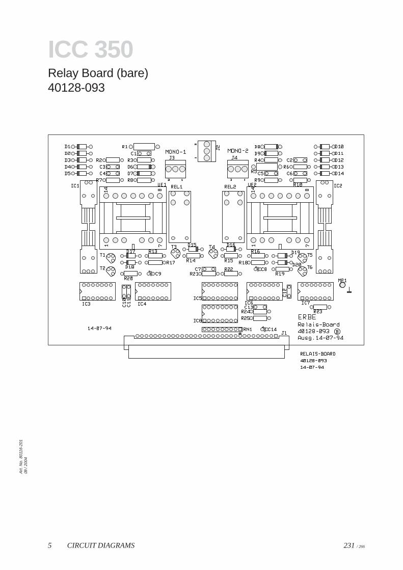
5 CIRCUIT DIAGRAMS 231 / 266
Art
. No.
801
16-2
0109
/ 20
04
ICC 350Relay Board (bare)40128-093
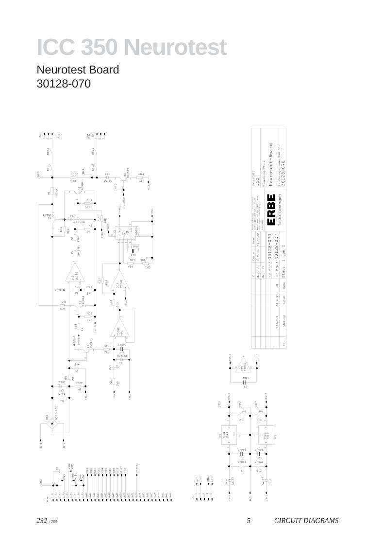
232 / 266 5 CIRCUIT DIAGRAMS
ICC 350 NeurotestNeurotest Board30128-070
AE
NE
1
Die
se Z
eic
hn
un
gis
t u
rhe
be
r-
oh
ne
un
sere
Ge
ne
hm
igu
ng
Be
ne
nn
un
g/T
itle
Ze
ich
nu
ng
snu
mm
er/
DW
G.N
O
Ge
rt/U
NIT
We
iterg
ab
e u
nd
Ve
rvie
lfltig
un
gre
chtli
ch g
esc
htz
t,d
ah
er
un
zuls
sig
Da
tum
Na
me
Ge
zeic
h.
Ge
pr
ft
LP
un
.:
LP
bs.
:
Bla
ttvo
nD
atu
mN
am
en
de
run
gN
r.
Ne
uro
test
-Bo
ard
ICC
30
12
8-0
70
30
12
8-0
70
40
12
8-0
27
M.F
ritz
214
-06
-93
C
14
.6.9
3M
FR
36
=3
k3
+-
~ ~
BR
1
B2
50
C8
00
C8
+
10uF
C9
+
100uF
C10
+
100uF
C12
+
1uF
C11
+
1uF
C1
100nF
C2
100nF
C3
68nF
C13
0u047
C14
0u33
D2
9V1 D6
1N4148
D1
1
BA
15
9
D1
1N
41
48
D1
2
BA
15
9
D7
9V
1
D13
BA159
F1
62
mA
I
G
O
78
xx7
81
5
IC1
IO
G
IC2
79
xx7
91
5
DG
ND
Fo
ut
RT
CT
CT
Vin
U F
+ -
IC4
AD
65
4
IC3
+- TL
08
2IC3
+- TL
08
2
-+
IC3
TL
08
2
IC6
+ -TL
08
2
J1
J2
J4 J5
MP
5
MP
3
MP
2
MP
6
MP
4
MP
1
MP
9
R1
820k
R4
220R
R9
10
k
R12
390R
R2
3
10
k
R1
3
10
k
R22
220k
R15
10k
R3
1k
R5
47
0R
R3
8
8k2
R2
1
1k5
R1
4
10
k
R7
390R
R39
1k5
R8
27k
R6
27k
R2
10k
R24
10k
R1
9
1k
RE
L1
RE
L1
RE
L2
RE
L2
BC
55
7T
5
T4
BU
X8
4
T3BUX84
T2
BU
X8
4T
1B
UX
84
TP1
10k
TY1
X0303
CS
12
CS
13
RE
SE
T
CL
R
ES
D0
ES
D1
ES
D2
ES
D3
ES
D4
ES
D5
ES
D6
ES
D7
FR
ES
FT
ES
T
GN
D
I-F
RE
Q
I-N
EU
RO
J2-1
J2-1
J2-2
J2-2
J2-5
J2-5
J2-5
NEG15
NE
G1
5
NE
G1
5
NE
G1
5
NU
LL
NU
LL
NU
LL
NU
LL
NU
LL
NU
LL
NU
LL
NU
LL
+2
4V
PO
S1
5
PO
S1
5
PO
S1
5
U-S
TE
UE
R
Vcc
+5
V
+1
5V
Vd
d
Ve
e-1
5V
2
13
1
23
7 621
58
34
2 3
1
6 5
7
48
65
7
A1
A1
0
A1
1
A1
2
A1
3
A1
4
A1
5
A1
6
A1
7
A1
8
A1
9
A2
A2
0
A2
1
A2
2
A2
3
A2
4
A2
5
A2
6
A2
7
A2
8
A2
9
A3
A3
0
A3
1
A3
2
A4
A5
A6
A7
A8
A9 1 2 3 4 5
1 2 3 1 2 3
2
3 1
1
2 3
1
23
1
2 3
1
2 3
3
2
1

5 CIRCUIT DIAGRAMS 233 / 266
Art
. No.
801
16-2
0109
/ 20
04
ICC 350 NeurotestNeurotest Board30128-070
2
Die
se Z
eic
hn
un
gis
t u
rhe
be
r-
oh
ne
un
sere
Ge
ne
hm
igu
ng
Be
ne
nn
un
g/T
itle
Ze
ich
nu
ng
snu
mm
er/
DW
G.N
O
Ge
rt/U
NIT
We
iterg
ab
e u
nd
Ve
rvie
lfltig
un
gre
chtli
ch g
esc
htz
t,d
ah
er
un
zuls
sig
Da
tum
Na
me
Ge
zeic
h.
Ge
pr
ft
LP
un
.:
LP
bs.
:
Bla
ttvo
nD
atu
mN
am
en
de
run
gN
r.
Ne
uro
test
-Bo
ard
ICC
30
12
8-0
70
30
12
8-0
70
40
12
8-0
27
M.F
ritz
214
-06
-93
C
14
.6.9
3M
FR
36
=3
k3
C6
68nF
C4
68nF
C7
68nF
C5
68nF
D5
1N
41
48
D8
1N
41
48
D9
1N
41
48
D1
0
1N
41
48
D4
1N
41
48
D3
1N
41
48
D1
5
1N
41
48
D1
6
1N
41
48
rot
D1
4
1DR C
1 40
17
4
IC1
4
IC1
3
UL
N2
00
4A
IC8
CN
Y6
6
IC9
CN
Y6
6
IC1
0
CN
Y6
6
IC1
1
CN
Y6
6
IC1
2
CN
Y6
6
IC7
CN
Y6
6
IC6
+- TL
08
2
-+
IC6
TL
08
2
0 1 2 3 4 5 6 7 8 9
1 2 4 8IC5
-+B
CD
/DE
C
40
28
MP
7
R3
1
1k3 R
32
1k3 R
33
1k3 R
34
1k3 R
35
2k2
R37
1k5
R2
5
30
k R2
6
13
k R2
7
7k5 R
28
4k3 R
17
2k4
R30
8k2
R11
220k
R29
1k3
R36
3k3
R10
3k3R20
3k3R18
3k3R16
3k3
RE
L1
RE
L2
CS
12
RE
SE
T
CL
R
ES
D0
ES
D1
ES
D2
ES
D3
ES
D4
ES
D5
FR
ES
FT
ES
T
GN
D
GN
D
GN
D
I-F
RE
Q
I-N
EU
RO
NE
G1
5
NE
G1
5
NU
LL
NU
LL
NU
LL
NU
LL
+2
4V
PO
S1
5
PO
S1
5
PO
S1
5
PO
S1
5
U-S
TE
UE
R
+1
5V
Vd
d
+1
5V
Vd
d
+1
5V
Vd
d
+1
5V
Vd
d
+1
5V
Vd
d
+1
5V
Vd
d
+1
5V
Vd
d
1 11
10
67
13
12
45
32
14
15
9
1 2 3 4 5 7 6
16
15
14
13
12
10
11
89
16
9 81 1
69 8
1 16
9 81 1
69 8
1 16
9 81
16
9 81
2 3
1
48
10
13
12
11
16 8
3 14
2 15
1 6 7 4 9 5

234 / 266 5 CIRCUIT DIAGRAMS
ICC 350 NeurotestNeurotest Board40128-027
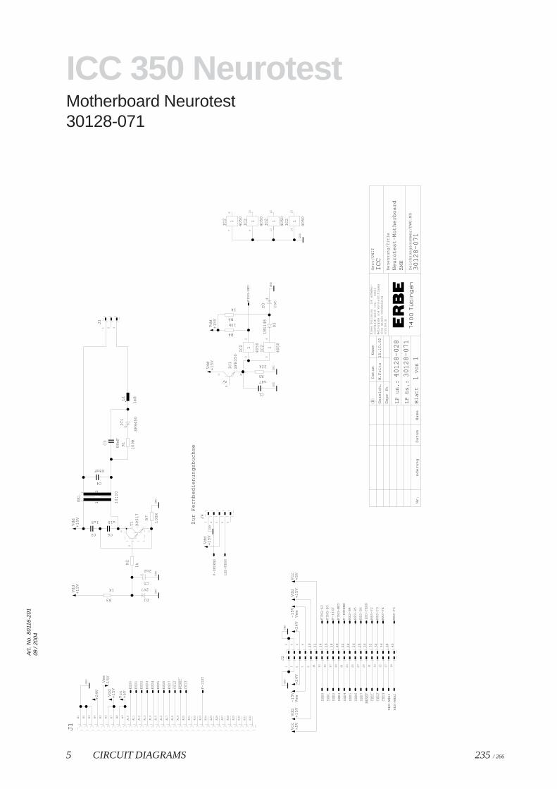
5 CIRCUIT DIAGRAMS 235 / 266
Art
. No.
801
16-2
0109
/ 20
04
ICC 350 NeurotestMotherboard Neurotest30128-071
Zu
r F
ern
be
die
nu
ng
sbu
chse
Die
se Z
eic
hn
un
gis
t u
rhe
be
r-
oh
ne
un
sere
Ge
ne
hm
igu
ng
Be
ne
nn
un
g/T
itle
Ze
ich
nu
ng
snu
mm
er/
DW
G.N
O
Ge
rt/U
NIT
We
iterg
ab
e u
nd
Ve
rvie
lfltig
un
gre
chtli
ch g
esc
htz
t,d
ah
er
un
zuls
sig
Da
tum
Na
me
Ge
zeic
h.
Ge
pr
ft
LP
un
.:
LP
bs.
:
Bla
ttvo
nD
atu
mN
am
en
de
run
gN
r.
M.F
ritz
ICC
30
12
8-0
71
30
12
8-0
71
40
12
8-0
28
11
B
15
.10
.92
Ne
uro
test
-Mo
the
rbo
ard
ZM
K
C3
68
nF
C4
68nF
C6
u15
C2
1u5
C5
+
2u2
C1
u47
D2
1N
41
48
D1
2V7
rot
D3
IC1
SF
H4
50
SF
H3
50
IC1
IC2
40
50
1
IC2
40
50
1
IC2
40
50
1
IC2
40
50
1
IC2
40
50
1
IC2
40
50
1
J1
J3
J4
J2
L1
1m
8
R1
10
0R
R7
10
0R
R2
1k
R3
1k
R5
22k
R4
10k
R6
1k
T1
BC
51
7
UE
1
10
:10
12
CS
11
CS
12
CS
12
CS
13
CS
13
RE
SE
T
RE
SE
T
ES
D0
ES
D0
ES
D1
ES
D1
ES
D2
ES
D2
ES
D3
ES
D3
ES
D4
ES
D4
ES
D5
ES
D5
ES
D6
ES
D6
ES
D7
ES
D7
F-I
IST
F-I
IST
F-I
NT
EN
S
F-I
NT
EN
S
FIN
G-A
3
FIN
G-B
3
FIN
G-N
EU
FIN
G-N
EU
GN
D
GN
D
GN
D
GN
DG
ND
GN
D
GN
DG
ND
GN
D
GN
D
GN
D
LE
D-F
ER
N
LE
D-F
ER
N
+2
4V
+2
4V
+2
4V
RE
S-A
NA
1
RE
S-A
NA
2
RE
S-B
4
RE
S-B
5
RE
S-B
6
RE
S-F
2
RE
S-F
3
RE
S-F
4
RE
S-F
6
Vcc
+5
V
Vcc
+5
V
Vcc
+5
V+
15
VV
dd
+1
5V
Vd
d
+1
5V
Vd
d
+1
5V
Vd
d+
15
VV
dd
+1
5V
Vd
d
+1
5V
Vd
d
+1
5V
Vd
dV
ee
-15
V
Ve
e-1
5V
Ve
e-1
5V
B
C E
32
54
76
91
0
11
12
14
15
A1
A1
0
A1
1
A1
2
A1
3
A1
4
A1
5
A1
6
A1
7
A1
8
A1
9
A2
A2
0
A2
1
A2
2
A2
3
A2
4
A2
5
A2
6
A2
7
A2
8
A2
9
A3
A3
0
A3
1
A3
2
A4
A5
A6
A7
A8
A9
1 2 3
1 2 3 4 5
1
10
11
12
13
14
15
16
17
18
19
2
20
21
22
23
24
25
26
27
28
29
3
30
31
32
33
34
35
36
37
38
39
4
40
56
78
9
2
3 1
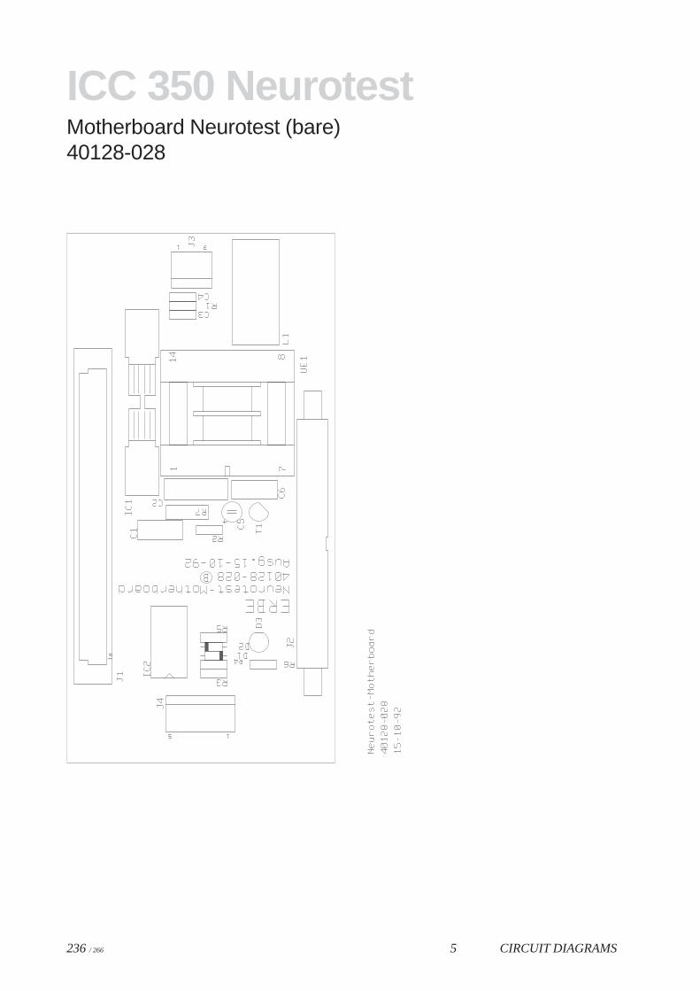
236 / 266 5 CIRCUIT DIAGRAMS
ICC 350 NeurotestMotherboard Neurotest (bare)40128-028
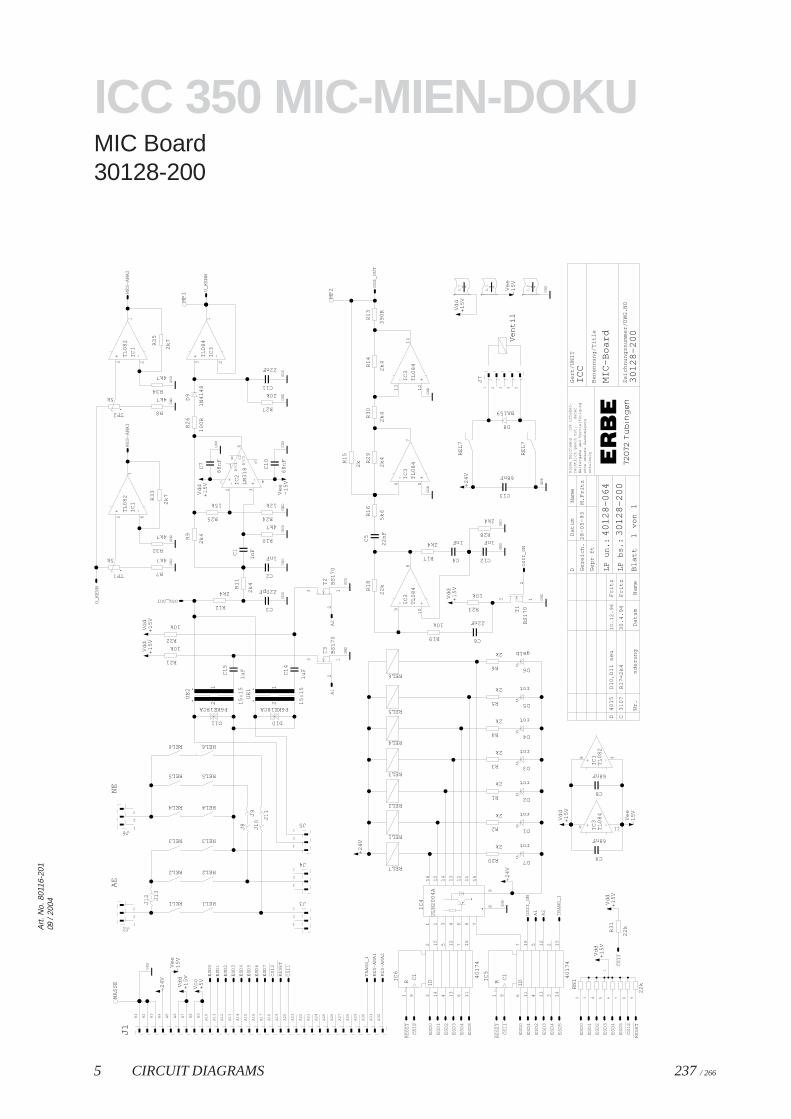
5 CIRCUIT DIAGRAMS 237 / 266
Art
. No.
801
16-2
0109
/ 20
04
ICC 350 MIC-MIEN-DOKUMIC Board30128-200
1
AE
NE
Ve
ntil
30
.4.9
4F
ritzFritz
R1
7=
2k4
31
07
D C
40
15
D1
0,D
11
ne
u1
0.1
2.9
6
Die
se Z
eic
hn
un
gis
t u
rhe
be
r-
oh
ne
un
sere
Ge
ne
hm
igu
ng
Be
ne
nn
un
g/T
itle
Ze
ich
nu
ng
snu
mm
er/
DW
G.N
O
Ge
rt/U
NIT
We
iterg
ab
e u
nd
Ve
rvie
lfltig
un
gre
chtli
ch g
esc
htz
t,d
ah
er
un
zuls
sig
Da
tum
Na
me
Ge
zeic
h.
Ge
pr
ft
LP
un
.:
LP
bs.
:
Bla
ttvo
nD
atu
mN
am
en
de
run
g
M.F
ritz
ICC
MIC
-Bo
ard
30
12
8-2
00
30
12
8-2
00
40
12
8-0
64
1
28
-05
-93
D
Nr.
0.7
0.7
1.0
C13
68nF
C1
5
1u
F C1
4
1u
F
C9
68nF
C4
1nF
C12
1nFC5
22
nF
C6
22nF
C8
68nF
C3
220pF
C1
1n
F
C7
68
nF
C1
0
68
nF
C11
22nF
C2
1nF
D10
P6KE18CA
D11
P6KE18CA
rot
D7
rot
D1
gelb
D6
rot
D2
D8
BA159
rot
D3
rot
D4
rot
D5
D9
1N
41
48
1DR C
1 40
17
4
IC6
1DR C
1 40
17
4
IC5
IC4
UL
N2
00
4A
IC2
+-+
- LM
31
8B
/C3C2
B/C
1
IC3
+ -TL
08
4
IC3
+- TL
08
4
IC3
+- TL
08
4
IC3
+- TL
08
4
-+
IC3
TL
08
4
IC1
+ -TL
08
2
IC1
+ -TL
08
2
-+
IC1
TL
08
2
J1
J4
J2
J6
J7
J5
J12 J1
3
J8
J9J1
0
J11
J3
MA
SS
E
MP
1
MP
2
R20
2k
R2
2k
R6
2k
R1
2k
R3
2k
R4
2k
R5
2k
R25
15k
R24
12k
R12
2k4
R1
1
2k4
R2
6
10
0R
R27
20k
R10
4k7
R9
2k4
R22
10k
R21
10k
R19
10k
R1
8
22
k
R1
6
5k6
R2
9
2k4
R3
0
2k4
R1
4
2k4
R1
5
2k
R1
3
39
0R
R17
2k4
R28
2k4
R23
10k
R3
1
22
k
R7
4k7
R8
4k7
R32
4k7
R3
3
2k7
R34
4k7
R3
5
2k7
REL1 REL1
REL6 REL6
REL1
REL6
RE
L7
RE
L7
REL7REL2REL2
REL2
REL3 REL3
REL4 REL4
REL5 REL5 REL3
REL4
REL5
RN
1
22
k
BS
17
0
T3
BS
17
0
T2
BS
17
0T1
TP1
5k
TP2
5k
UE
2
15
:15
12
UE
1
15
:15
12
CS
11 C
S1
1
CS
11
CS
12
CS
12
CS
12
RE
SE
T
RE
SE
T
RE
SE
T
RE
SE
T
A1
A1
A2
A2
ES
D0
ES
D0
ES
D0
ES
D0
ES
D1
ES
D1
ES
D1
ES
D1
ES
D2
ES
D2
ES
D2
ES
D2
ES
D3
ES
D3
ES
D3
ES
D3
ES
D4
ES
D4
ES
D4
ES
D4
ES
D5
ES
D5
ES
D5
ES
D5
ES
D6
ES
D7
GN
D
GN
D
GN
DG
ND
GN
DG
ND
GN
DG
ND
GN
DG
ND
GN
D
GN
DG
ND
GN
D
GN
DG
ND
GN
DG
ND
GN
DG
ND
GN
D
GN
D
GN
D
OSZ_OUT
OS
Z_
OU
T
OS
ZI_
ON
OS
ZI_
ON
+2
4V
+2
4V
+2
4V
+2
4V
RE
S-A
NA
1
RE
S-A
NA
1
RE
S-A
NA
2
RE
S-A
NA
2
TR
AN
S_
1
TR
AN
S_
1
U_
KE
NN
U_
KE
NN
Vcc
+5
V+
15
VV
dd
+1
5V
Vd
d
+1
5V
Vd
d
+1
5V
Vd
d+
15
VV
dd
+1
5V
Vd
d
+1
5V
Vd
d+
15
VV
dd
+1
5V
Vd
d
Ve
e-1
5V
Ve
e-1
5V
Ve
e-1
5V
Ve
e-1
5V
1 32
14
15
45
13
12
67
11
10
9 1 67
11
10
45
13
12
32
14
15
9
1 2 3 4 5 6 7
16
15
14
13
12
11
10
89
2
1
85
3
4
6
7
23
1
9
10
8
6 5
7
13
12
14
114
65
7
23
1
48
A1
A1
0
A1
1
A1
2
A1
3
A1
4
A1
5
A1
6
A1
7
A1
8
A1
9
A2
A2
0
A2
1
A2
2
A2
3
A2
4
A2
5
A2
6
A2
7
A2
8
A2
9
A3
A3
0
A3
1
A3
2
A4
A5
A6
A7
A8
A9
1
2
3
1
2
3
1
2
3
1 2 3 4 5
1
2
3
1
2
3
1
2 3 4 5 6 7 8 9
3
2
1
3
2
1
3
2
1
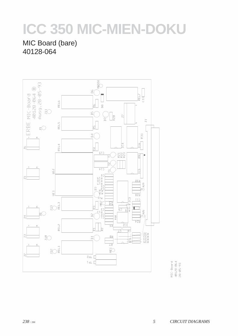
238 / 266 5 CIRCUIT DIAGRAMS
ICC 350 MIC-MIEN-DOKUMIC Board (bare)40128-064
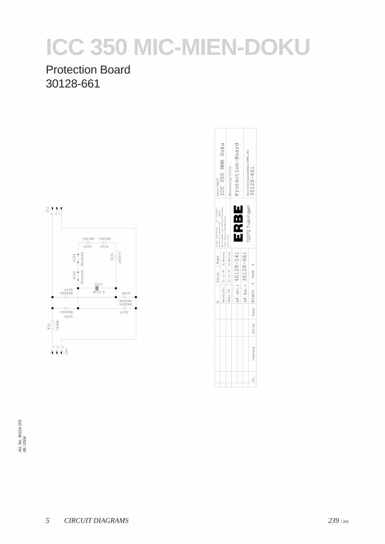
5 CIRCUIT DIAGRAMS 239 / 266
Art
. No.
801
16-2
0109
/ 20
04
ICC 350 MIC-MIEN-DOKUProtection Board30128-661
1
E.W
ern
er
01
-12
-97
E.W
ern
er
01
-12
-97
Die
se Z
eic
hn
un
gis
t u
rhe
be
r-
oh
ne
un
sere
Ge
ne
hm
igu
ng
Be
ne
nn
un
g/T
itle
Ze
ich
nu
ng
snu
mm
er/
DW
G.N
O
Ge
rt/U
NIT
We
iterg
ab
e u
nd
Ve
rvie
lfltig
un
gre
chtli
ch g
esc
htz
t,d
ah
er
un
zuls
sig
Da
tum
Na
me
Ge
zeic
h.
Ge
pr
ft
LP
un
.:
LP
bs.
:
Bla
ttvo
nD
atu
mN
am
en
de
run
g
A
Nr.
ICC
35
0 M
MH
Do
ku
1
Pro
tect
ion
-Bo
ard
30
12
8-6
61
40
12
8-1
41
30
12
8-6
61
C100
0.01uF
D1
01
1N
53
73
D102
1N5383
D103
1N5383
D1
04
Bru
eck
e
D1
05
Bru
eck
e
D106
NS2004 D107
NS2004
D108
NS2004
D109NS2004
F1
0
25
0m
A
J10
J11
1231 2 3
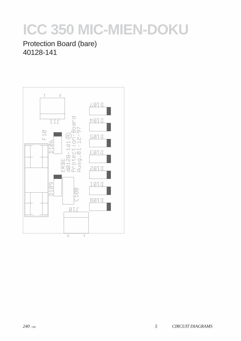
240 / 266 5 CIRCUIT DIAGRAMS
ICC 350 MIC-MIEN-DOKUProtection Board (bare)40128-141

Appendix APart Numbers

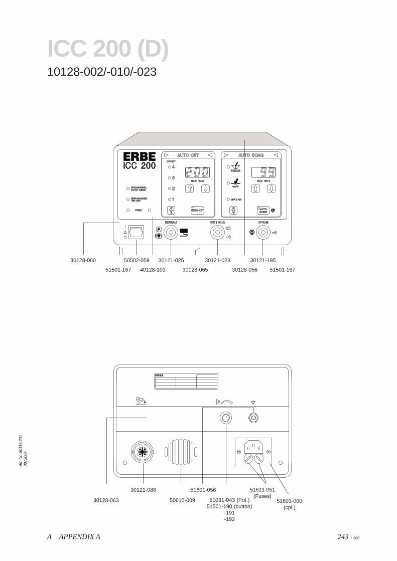
A APPENDIX A 243 / 266
Art.
-No.
801
16-2
0109
/ 20
04
ICC 200 (D)10128-002/-010/-023
30128-060
40128-103
50502-059 30121-195
51501-167
30121-025
30128-065
30121-023
30128-056 51501-167
30121-086 51611-051(Fuses)
51603-000(cpl.)
51601-056
50610-009 51031-043 (Pot.)51501-190 (button)
-191-192
30128-063
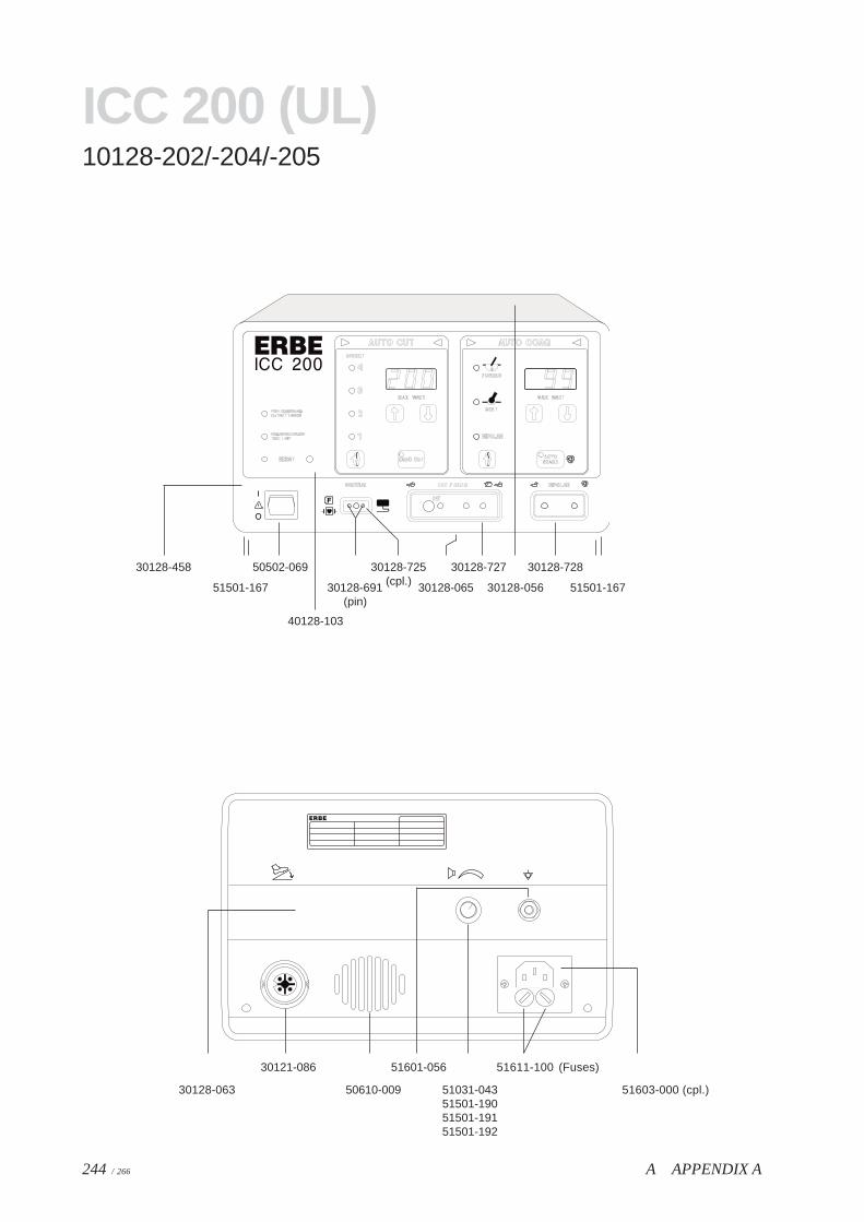
A APPENDIX A244 / 266
ICC 200 (UL)10128-202/-204/-205
30128-458
40128-103
50502-069 30128-728
51501-167 30128-065
30128-727
30128-056 51501-167
30121-086
51603-000 (cpl.)
51601-056
50610-009 51031-04351501-19051501-19151501-192
30128-063
30128-691(pin)
30128-725(cpl.)
51611-100 (Fuses)
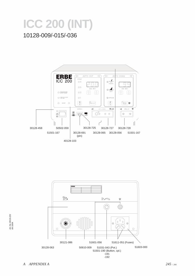
A APPENDIX A 245 / 266
Art.
-No.
801
16-2
0109
/ 20
04
ICC 200 (INT)10128-009/-015/-036
30128-458
40128-103
50502-059 30128-728
51501-167 30128-065
30128-727
30128-056 51501-167
30121-086 51611-051 (Fuses)
51603-000
51601-056
50610-009 51031-043 (Pot.)51501-190 (Button, cpl.)
-191-192
30128-063
30128-691(pin)
30128-725
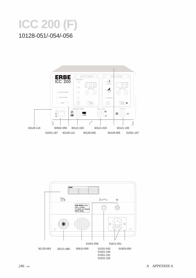
A APPENDIX A246 / 266
ICC 200 (F)10128-051/-054/-056
30128-116
40128-112
50502-059 30121-195
51501-167
30121-025
30128-065
30121-023
30128-056 51501-167
30121-086
51611-051
51603-000
51601-056
50610-009 51031-04351501-19051501-19151501-192
30128-063
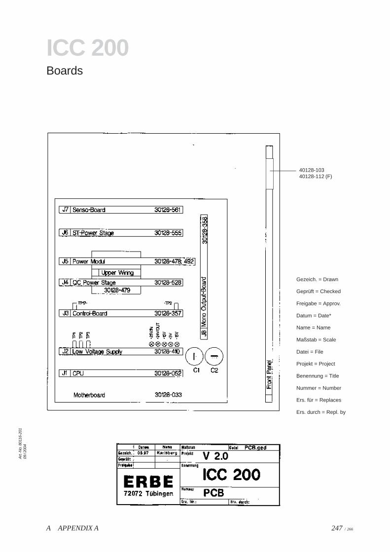
A APPENDIX A 247 / 266
Art.
-No.
801
16-2
0109
/ 20
04
ICC 200Boards
40128-10340128-112 (F)
Gezeich. = Drawn
Geprüft = Checked
Freigabe = Approv.
Datum = Date*
Name = Name
Maßstab = Scale
Datei = File
Projekt = Project
Benennung = Title
Nummer = Number
Ers. für = Replaces
Ers. durch = Repl. by
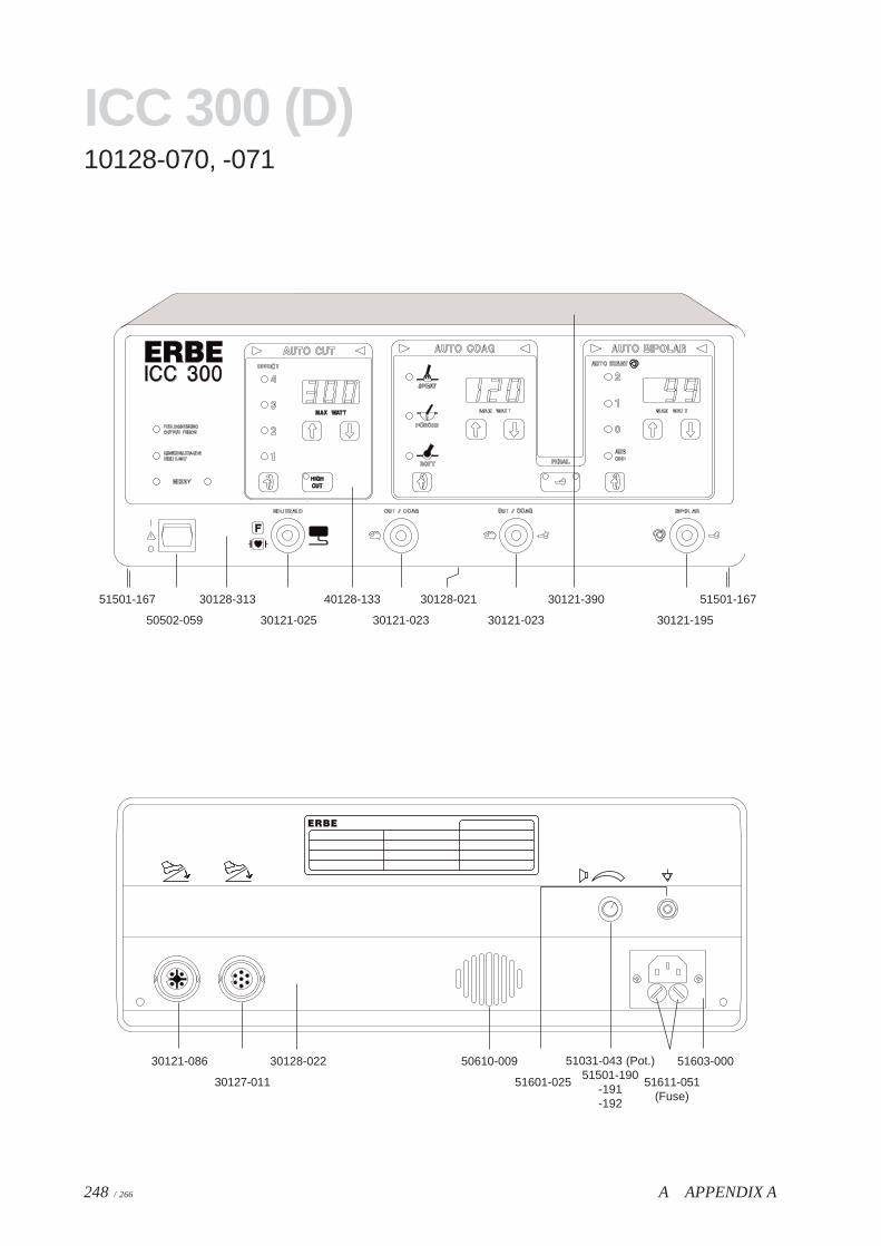
A APPENDIX A248 / 266
ICC 300 (D)10128-070, -071
30121-086
30127-011
30128-022 50610-009
51601-025 51611-051(Fuse)
51603-00051031-043 (Pot.)51501-190
-191-192
51501-167
50502-059 30121-025
40128-133
30121-023 30121-023
30121-390
30121-195
51501-16730128-02130128-313
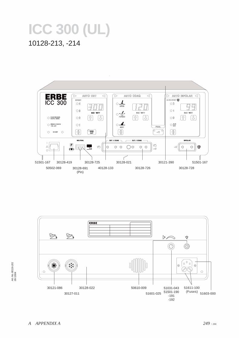
A APPENDIX A 249 / 266
Art.
-No.
801
16-2
0109
/ 20
04
ICC 300 (UL)10128-213, -214
30121-086
30127-011
30128-022 50610-009
51601-025
51611-100(Fuses)
51031-04351501-190
-191-192
50502-069 40128-133 30128-726
30121-390
30128-728
51501-16730128-02130128-41951501-167
30128-691(Pin)
30128-725
51603-000
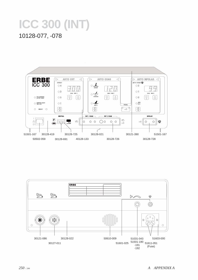
A APPENDIX A250 / 266
ICC 300 (INT)10128-077, -078
30121-086
30127-011
30128-022 50610-009
51601-025 51611-051(Fuse)
51603-00051031-04351501-190
-191-192
50502-059 30128-691 40128-133 30128-726
30121-390
30128-728
51501-16730128-02130128-41951501-167 30128-725
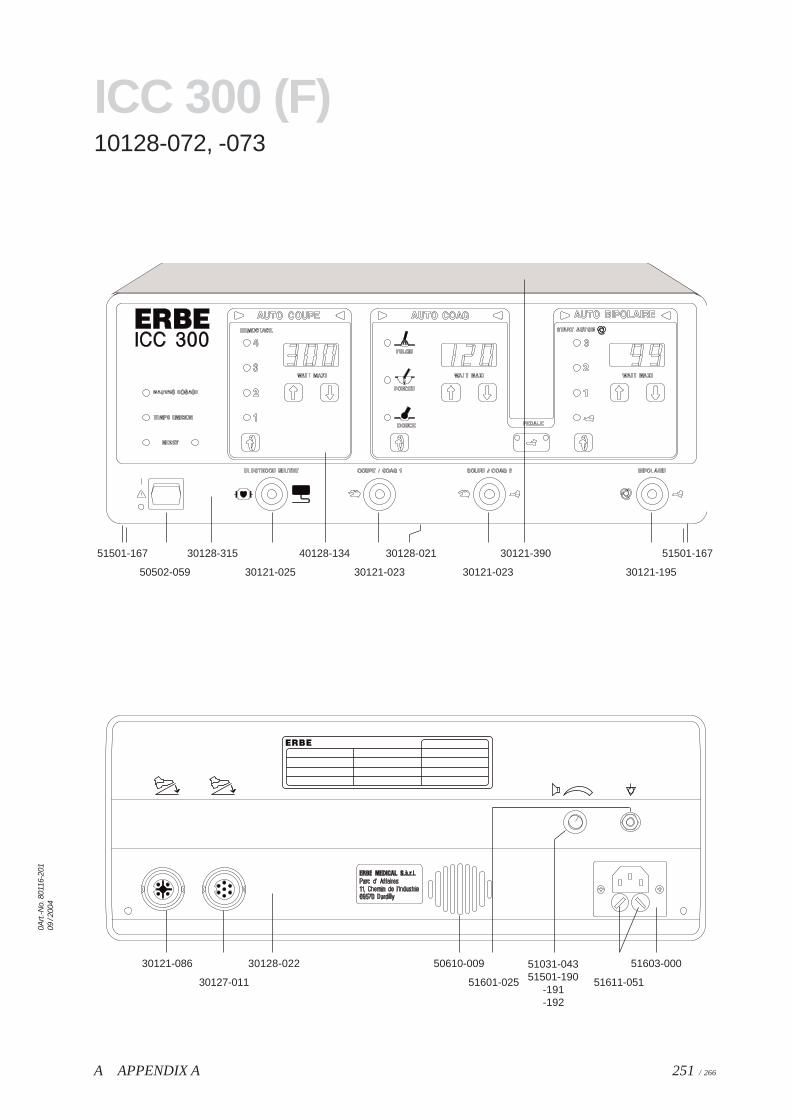
A APPENDIX A 251 / 266
0Art.
-No.
801
16-2
0109
/ 20
04
ICC 300 (F)10128-072, -073
51501-167
50502-059 30121-025
40128-134
30121-023 30121-023
30121-390
30121-195
51501-16730128-02130128-315
30121-086
30127-011
30128-022 50610-009
51601-025 51611-051
51603-00051031-04351501-190
-191-192
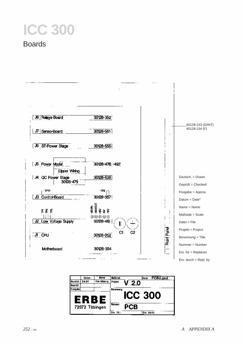
A APPENDIX A252 / 266
ICC 300Boards
40128-133 (D/INT)40128-134 (F)
Gezeich. = Drawn
Geprüft = Checked
Freigabe = Approv.
Datum = Date*
Name = Name
Maßstab = Scale
Datei = File
Projekt = Project
Benennung = Title
Nummer = Number
Ers. für = Replaces
Ers. durch = Repl. by
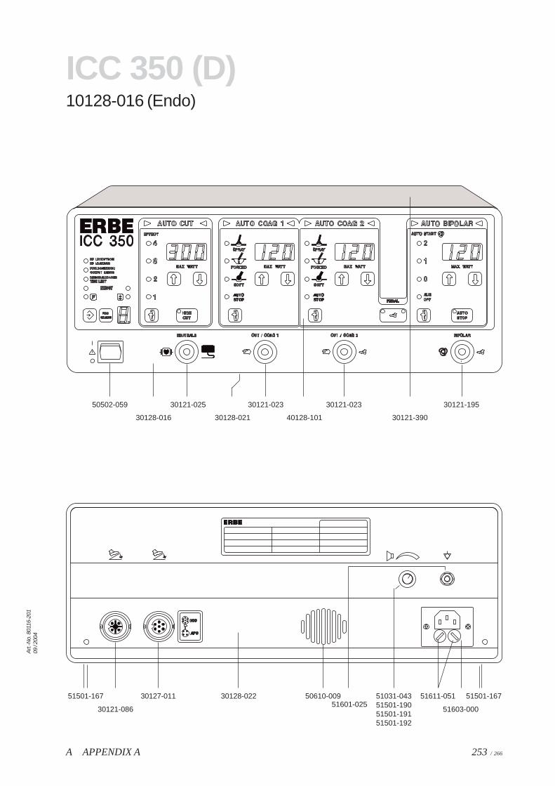
A APPENDIX A 253 / 266
Art.
-No.
801
16-2
0109
/ 20
04
ICC 350 (D)10128-016 (Endo)
50502-059
40128-10130128-016 30121-390
30121-025 30121-023 30121-023 30121-195
30128-021
51601-02551501-16751501-167
30121-086
30127-011
51603-000
30128-022 50610-009 51031-04351501-19051501-19151501-192
51611-051
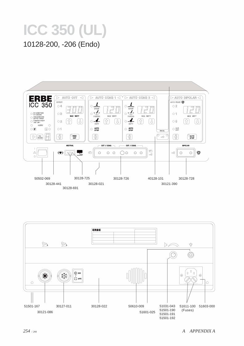
A APPENDIX A254 / 266
ICC 350 (UL)10128-200, -206 (Endo)
51603-00051501-167
30121-086
30127-011 30128-022 50610-009 51031-04351501-19051501-19151501-192
51611-100(Fuses)
50502-069 40128-101
30128-441 30121-390
30128-726 30128-728
30128-02130128-691
30128-725
51601-025
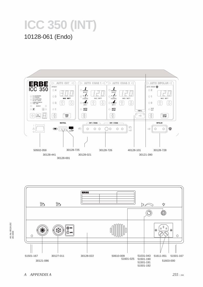
A APPENDIX A 255 / 266
Art.
-No.
801
16-2
0109
/ 20
04
ICC 350 (INT)10128-061 (Endo)
50502-059 40128-101
30128-441 30121-390
30128-726 30128-728
30128-02130128-691
30128-725
51601-02551501-16751501-167
30121-086
30127-011
51603-000
30128-022 50610-009 51031-04351501-19051501-19151501-192
51611-051
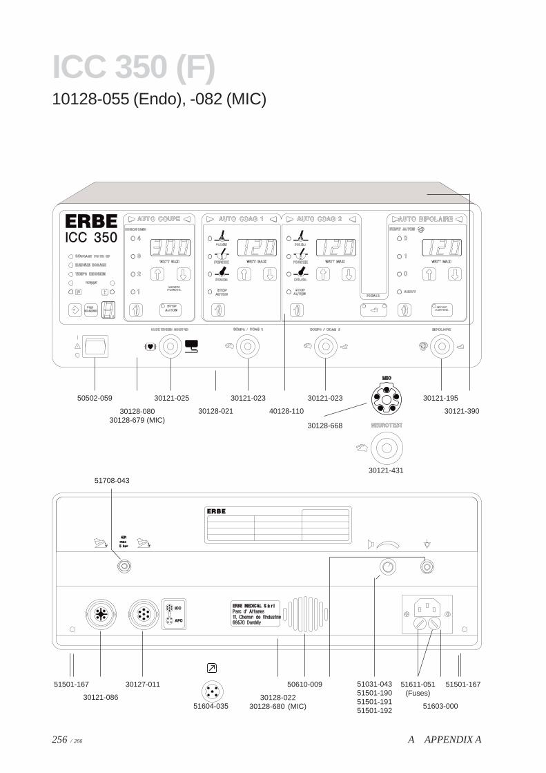
A APPENDIX A256 / 266
ICC 350 (F)10128-055 (Endo), -082 (MIC)
50502-059
40128-11030128-08030128-679 (MIC)
30121-390
30121-025 30121-023 30121-023 30121-195
30128-021
30128-668
51501-16751501-167
30121-086
30127-011
51603-00030128-022
30128-680 (MIC)
50610-009 51031-04351501-19051501-19151501-192
51611-051(Fuses)
51604-035
51708-04330121-431
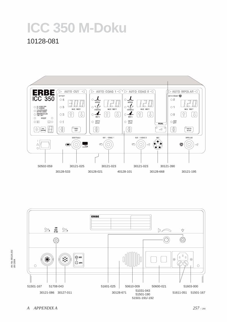
A APPENDIX A 257 / 266
Art.
-No.
801
16-2
0109
/ 20
04
ICC 350 M-Doku10128-081
50502-059
40128-10130128-533
30121-39030121-025 30121-023 30121-023
30121-19530128-021 30128-668
50600-02151501-167
30121-086
51708-043
30127-011
51601-025 50610-009
51611-051
51603-000
51501-16751031-04351501-190
51501-191/-192
30128-671
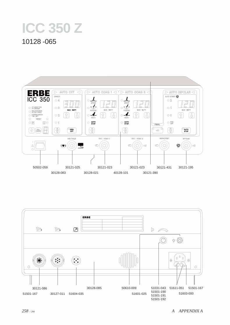
A APPENDIX A258 / 266
ICC 350 Z10128 -065
50502-059
40128-10130128-083 30121-390
30121-025 30121-023 30121-023 30121-195
30128-021
51501-167
51501-167
30121-086
30127-011 51603-000
30128-085 50610-009 51031-04351501-19051501-19151501-192
51611-051
51601-02551604-035
30121-431
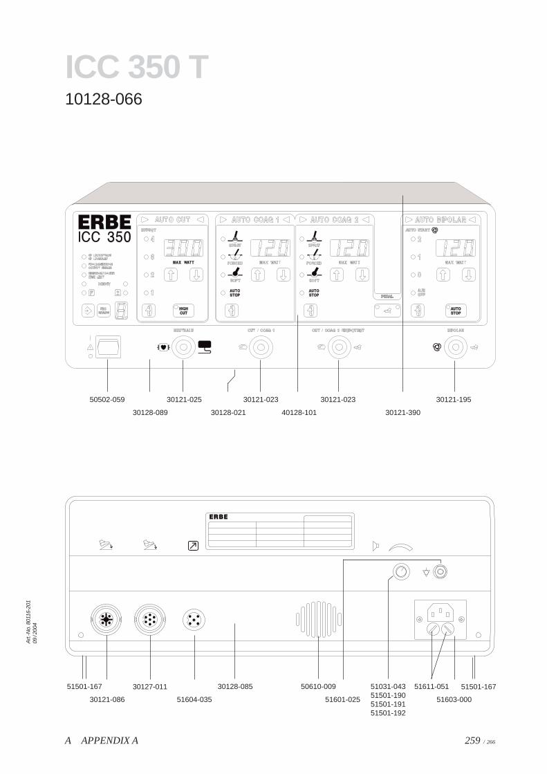
A APPENDIX A 259 / 266
Art.
-No.
801
16-2
0109
/ 20
04
ICC 350 T10128-066
50502-059
40128-10130128-089 30121-390
30121-025 30121-023 30121-023 30121-195
30128-021
51501-167
30121-086
30127-011
51604-035 51603-000
30128-085 50610-009 51031-04351501-19051501-19151501-192
51611-051 51501-167
51601-025
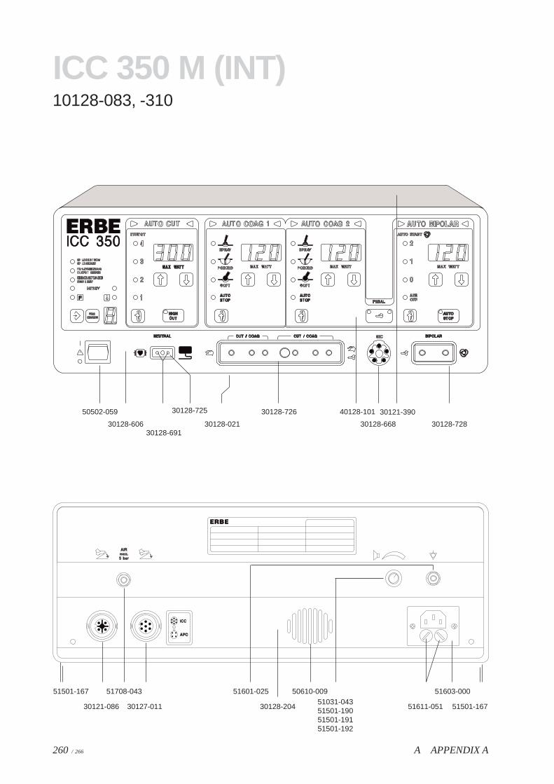
A APPENDIX A260 / 266
ICC 350 M (INT)10128-083, -310
50502-059 40128-101
30128-606
30121-39030128-726
30128-72830128-021 30128-668
51501-167
30121-086
51708-043
30127-011
51601-025 50610-009
51611-051
51603-000
51501-16751031-04351501-19051501-19151501-192
30128-204
30128-691
30128-725

A APPENDIX A 261 / 266
Art.
-No.
801
16-2
0109
/ 20
04
ICC 350 M10128-080
50502-059
40128-10130128-533
30121-39030121-025 30121-023 30121-023
30121-19530128-021 30128-668
51501-167
30121-086
51708-043
30127-011
51601-025 50610-009
51611-051
51603-000
51501-16751031-04351501-190
51501-191/-192
30128-671
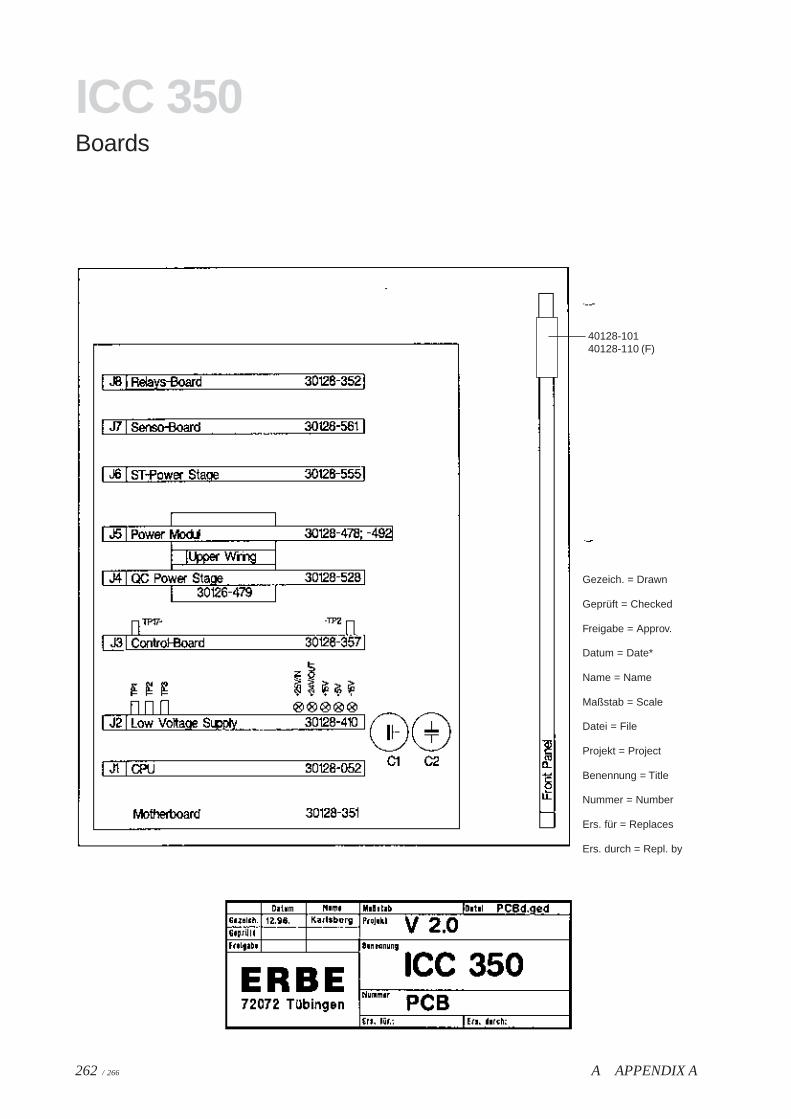
A APPENDIX A262 / 266
ICC 350Boards
40128-10140128-110 (F)
Gezeich. = Drawn
Geprüft = Checked
Freigabe = Approv.
Datum = Date*
Name = Name
Maßstab = Scale
Datei = File
Projekt = Project
Benennung = Title
Nummer = Number
Ers. für = Replaces
Ers. durch = Repl. by

AppendixB
Abbreviations, Notes,Addresses

264 / 266 B APPENDIX B

265/ 266B APPENDIX B
Art
. No.
: 801
16-2
0109
/ 20
04
AppendixAbbreviationsNotesAddresses
Abbreviations
The following list summarizes all those abbreviations and symbols which are used in this service manual.
Abbreviation means Abbreviation means
NE neutral electrode ö phase angle
| non-split NE V(p) volts (peak value)
|| split NE A(eff) amperes (r.m.s. value)
Parts lists
This service manual includes no parts lists. However, if you should need to refer to part numbers, please seeAppendix A.
Measuring equipment
For a list of recommended measuring equipment for servicing the units ICC 200, ICC 300 and ICC 350,please refer to this service manual (Chapter 1, Test program 16).
Diagrams of electrical dimensions
The diagrams of the electrical dimensions are not shown in this service manual. However, you will findthese printed in the instruction manuals for the respective unit.
Any questions?
This service manual has been put together carefully and was subjected to a continuous improvement processduring its creation by the Service Department and/or the Development Department at ERBE Elektromedizin.Nevertheless, you may still have questions; additionally, this manual cannot assume to be perfect andcompletely without error. In such cases, please contact:
Contents, formulation, structure, technicalinformation
Dipl.-Phys. Michael Grosse (Development Dept.)
Tel.: (+49) 70 71 / 755–254
E-mail: [email protected]
Technical questions regarding service and theunits
Service Manager Roland Bauer (Service Dept.)
Tel.: (+49) 70 71 / 755–454
E-mail: [email protected]

Your notes