Enhanced spatial near-infrared modulation of graphene...
11
Enhanced spatial near-infrared modulation of graphene-loaded perfect absorbers using plasmonic nanoslits Yijun Cai, 1 Jinfeng Zhu, 1,* Qing Huo Liu, 2 Timothy Lin, 3 Jianyang Zhou, 1 Longfang Ye, 1 and Zhiping Cai 4 1 Institute of Electromagnetics and Acoustics, Xiamen University, Xiamen 361005, China 2 Department of Electrical and Computer Engineering, Duke University, Durham, NC 27708, USA 3 Aegis Technology Inc., 12630 G Westminster Ave., Santa Ana, CA 92706, USA 4 Department of Electronic Engineering, Xiamen University, Xiamen 361005, China * [email protected] Abstract: Modulating spatial near-infrared light for ultra-compact electro- optic devices is a critical issue in optical communication and imaging applications. To date, spatial near-infrared modulators based on graphene have been reported, but they showed limited modulation effects due to the relatively weak light-graphene interaction. In combination with graphene and metallic nanoslits, we design a kind of ultrathin near-infrared perfect absorber with enhanced spatial modulation effects and independence on a wide range of incident angles. The modulated spectral shift of central wavelength is up to 258.2 nm in the near-infrared range, which is more promising in applications than state-of-the-art devices. The modulation enhancement is attributed to the plasmonic nanoslit mode, in which the optical electric field is highly concentrated in the deep subwavelength scale and the light-graphene interaction is significantly strengthened. The physical insight is deeply revealed by a combination of equivalent circuit and electromagnetic field analysis. The design principles are not only crucial for spatial near-infrared modulators, but also provide a key guide for developing active near-infrared patch nanoantennas based on graphene. ©2015 Optical Society of America OCIS codes: (240.6380) Spectroscopy, modulation; (310.6805) Theory and design; (230.4110) Modulators; (230.6120) Spatial light modulators; (240.6680) Surface plasmons. References and links 1. N. Liu, M. Mesch, T. Weiss, M. Hentschel, and H. Giessen, “Infrared perfect absorber and its application as plasmonic sensor,” Nano Lett. 10(7), 2342–2348 (2010). 2. T. Maier and H. Brückl, “Wavelength-tunable microbolometers with metamaterial absorbers,” Opt. Lett. 34(19), 3012–3014 (2009). 3. C. F. Guo, T. Sun, F. Cao, Q. Liu, and Z. Ren, “Metallic nanostructures for light trapping in energy-harvesting devices,” Light Sci. Appl. 3(4), e161 (2014). 4. S. A. Mann and E. C. Garnett, “Resonant nanophotonic spectrum splitting for ultrathin multijunction solar cells,” ACS Photonics 2(7), 816–821 (2015). 5. C. Wu, B. Neuner III, J. John, A. Milder, B. Zollars, S. Savoy, and G. Shvets, “Metamaterial-based integrated plasmonic absorber/emitter for solar thermo-photovoltaic systems,” J. Opt. 14(2), 024005 (2012). 6. J. Hao, L. Zhou, and M. Qiu, “Nearly total absorption of light and heat generation by plasmonic metamaterials,” Phys. Rev. B 83(16), 165107 (2011). 7. C. M. Watts, D. Shrekenhamer, J. Montoya, G. Lipworth, J. Hunt, T. Sleasman, S. Krishna, D. R. Smith, and W. J. Padilla, “Terahertz compressive imaging with metamaterial spatial light modulators,” Nat. Photonics 8(8), 605–609 (2014). 8. G. T. Reed, G. Mashanovich, F. Y. Gardes, and D. J. Thomson, “Silicon optical modulators,” Nat. Photonics 4(8), 518–526 (2010). 9. M. Liu, X. Yin, E. Ulin-Avila, B. Geng, T. Zentgraf, L. Ju, F. Wang, and X. Zhang, “A graphene-based broadband optical modulator,” Nature 474(7349), 64–67 (2011). 10. Y. Bao, S. Zhu, Y. Zhang, and Z. Fang, “Active control of graphene-based unidirectional surface plasmon launcher,” ACS Photonics 2(8), 1135–1140 (2015). 11. F. J. García de Abajo, “Graphene nanophotonics,” Science 339(6122), 917–918 (2013). #251935 Received 15 Oct 2015; revised 1 Dec 2015; accepted 1 Dec 2015; published 8 Dec 2015 © 2015 OSA 14 Dec 2015 | Vol. 23, No. 25 | DOI:10.1364/OE.23.032318 | OPTICS EXPRESS 32318
Transcript of Enhanced spatial near-infrared modulation of graphene...

Enhanced spatial near-infrared modulation of graphene-loaded perfect absorbers using
plasmonic nanoslits Yijun Cai,1 Jinfeng Zhu,1,* Qing Huo Liu,2 Timothy Lin,3 Jianyang Zhou,1 Longfang
Ye,1 and Zhiping Cai4 1Institute of Electromagnetics and Acoustics, Xiamen University, Xiamen 361005, China
2Department of Electrical and Computer Engineering, Duke University, Durham, NC 27708, USA 3Aegis Technology Inc., 12630 G Westminster Ave., Santa Ana, CA 92706, USA
4Department of Electronic Engineering, Xiamen University, Xiamen 361005, China *[email protected]
Abstract: Modulating spatial near-infrared light for ultra-compact electro-optic devices is a critical issue in optical communication and imaging applications. To date, spatial near-infrared modulators based on graphene have been reported, but they showed limited modulation effects due to the relatively weak light-graphene interaction. In combination with graphene and metallic nanoslits, we design a kind of ultrathin near-infrared perfect absorber with enhanced spatial modulation effects and independence on a wide range of incident angles. The modulated spectral shift of central wavelength is up to 258.2 nm in the near-infrared range, which is more promising in applications than state-of-the-art devices. The modulation enhancement is attributed to the plasmonic nanoslit mode, in which the optical electric field is highly concentrated in the deep subwavelength scale and the light-graphene interaction is significantly strengthened. The physical insight is deeply revealed by a combination of equivalent circuit and electromagnetic field analysis. The design principles are not only crucial for spatial near-infrared modulators, but also provide a key guide for developing active near-infrared patch nanoantennas based on graphene.
©2015 Optical Society of America
OCIS codes: (240.6380) Spectroscopy, modulation; (310.6805) Theory and design; (230.4110) Modulators; (230.6120) Spatial light modulators; (240.6680) Surface plasmons.
References and links
1. N. Liu, M. Mesch, T. Weiss, M. Hentschel, and H. Giessen, “Infrared perfect absorber and its application as plasmonic sensor,” Nano Lett. 10(7), 2342–2348 (2010).
2. T. Maier and H. Brückl, “Wavelength-tunable microbolometers with metamaterial absorbers,” Opt. Lett. 34(19), 3012–3014 (2009).
3. C. F. Guo, T. Sun, F. Cao, Q. Liu, and Z. Ren, “Metallic nanostructures for light trapping in energy-harvesting devices,” Light Sci. Appl. 3(4), e161 (2014).
4. S. A. Mann and E. C. Garnett, “Resonant nanophotonic spectrum splitting for ultrathin multijunction solar cells,” ACS Photonics 2(7), 816–821 (2015).
5. C. Wu, B. Neuner III, J. John, A. Milder, B. Zollars, S. Savoy, and G. Shvets, “Metamaterial-based integrated plasmonic absorber/emitter for solar thermo-photovoltaic systems,” J. Opt. 14(2), 024005 (2012).
6. J. Hao, L. Zhou, and M. Qiu, “Nearly total absorption of light and heat generation by plasmonic metamaterials,” Phys. Rev. B 83(16), 165107 (2011).
7. C. M. Watts, D. Shrekenhamer, J. Montoya, G. Lipworth, J. Hunt, T. Sleasman, S. Krishna, D. R. Smith, and W. J. Padilla, “Terahertz compressive imaging with metamaterial spatial light modulators,” Nat. Photonics 8(8), 605–609 (2014).
8. G. T. Reed, G. Mashanovich, F. Y. Gardes, and D. J. Thomson, “Silicon optical modulators,” Nat. Photonics 4(8), 518–526 (2010).
9. M. Liu, X. Yin, E. Ulin-Avila, B. Geng, T. Zentgraf, L. Ju, F. Wang, and X. Zhang, “A graphene-based broadband optical modulator,” Nature 474(7349), 64–67 (2011).
10. Y. Bao, S. Zhu, Y. Zhang, and Z. Fang, “Active control of graphene-based unidirectional surface plasmon launcher,” ACS Photonics 2(8), 1135–1140 (2015).
11. F. J. García de Abajo, “Graphene nanophotonics,” Science 339(6122), 917–918 (2013).
#251935 Received 15 Oct 2015; revised 1 Dec 2015; accepted 1 Dec 2015; published 8 Dec 2015 © 2015 OSA 14 Dec 2015 | Vol. 23, No. 25 | DOI:10.1364/OE.23.032318 | OPTICS EXPRESS 32318

12. A. Vakil and N. Engheta, “Transformation optics using graphene,” Science 332(6035), 1291–1294 (2011). 13. F. Bonaccorso, Z. Sun, T. Hasan, and A. C. Ferrari, “Graphene photonics and optoelectronics,” Nat. Photonics
4(9), 611–622 (2010). 14. Y. Yao, R. Shankar, M. A. Kats, Y. Song, J. Kong, M. Loncar, and F. Capasso, “Electrically tunable metasurface
perfect absorbers for ultrathin mid-infrared optical modulators,” Nano Lett. 14(11), 6526–6532 (2014). 15. L. Shao, X. Wang, H. Xu, J. Wang, J.-B. Xu, L.-M. Peng, and H.-Q. Lin, “Nanoantenna-sandwiched graphene
with giant spectral tuning in the visible-to-near-infrared region,” Adv. Opt. Mater. 2(2), 162–170 (2014). 16. E. Simsek, “Improving tuning range and sensitivity of localized SPR sensors with graphene,” IEEE Photonics
Technol. Lett. 25(9), 867–870 (2013). 17. X. Li, W. C. H. Choy, X. Ren, D. Zhang, and H. Lu, “Highly intensified surface enhanced Raman scattering by
using monolayer graphene as the nanospacer of metal film–metal nanoparticle coupling system,” Adv. Funct. Mater. 24(21), 3114–3122 (2014).
18. C. T. Phare, Y.-H. D. Lee, J. Cardenas, and M. Lipson, “Graphene electro-optic modulator with 30 GHz bandwidth,” Nat. Photonics 9(8), 511–514 (2015).
19. J. Zhu, Q. H. Liu, and T. Lin, “Manipulating light absorption of graphene using plasmonic nanoparticles,” Nanoscale 5(17), 7785–7789 (2013).
20. A. Alù and N. Engheta, “Theory, modeling and features of optical nanoantennas,” IEEE Trans. Antenn. Propag. 61(4), 1508–1517 (2013).
21. E. D. Palik, Handbook of Optical Constants of Solids (Academic, 1998). 22. T. Ishii and T. Sato, “Growth of single crystals of hexagonal boron nitride,” J. Cryst. Growth 61(3), 689–690
(1983). 23. Y. Liu, A. Chadha, D. Zhao, J. R. Piper, Y. Jia, Y. Shuai, L. Menon, H. Yang, Z. Ma, S. Fan, F. Xia, and W.
Zhou, “Approaching total absorption at near infrared in a large area monolayer graphene by critical coupling,” Appl. Phys. Lett. 105(18), 181105 (2014).
24. Y. Zhao, X. Li, Y. Du, G. Chen, Y. Qu, J. Jiang, and Y. Zhu, “Strong light-matter interactions in sub-nanometer gaps defined by monolayer graphene: toward highly sensitive SERS substrates,” Nanoscale 6(19), 11112–11120 (2014).
25. G. W. Hanson, “Dyadic Green’s functions and guided surface waves for a surface conductivity model of graphene,” J. Appl. Phys. 103(6), 064302 (2008).
26. N. M. R. Peres, F. Guinea, and A. H. Castro Neto, “Electronic properties of disordered two-dimensional carbon,” Phys. Rev. B 73(12), 125411 (2006).
27. Q. Zhang, X. Li, M. M. Hossain, Y. Xue, J. Zhang, J. Song, J. Liu, M. D. Turner, S. Fan, Q. Bao, and M. Gu, “Graphene surface plasmons at the near-infrared optical regime,” Sci. Rep. 4, 6559 (2014).
28. D. A. Kuzmin, I. V. Bychkov, and V. G. Shavrov, “Influence of graphene coating on speckle-pattern rotation of light in gyrotropic optical fiber,” Opt. Lett. 40(6), 890–893 (2015).
29. N. K. Emani, T.-F. Chung, A. V. Kildishev, V. M. Shalaev, Y. P. Chen, and A. Boltasseva, “Electrical modulation of fano resonance in plasmonic nanostructures using graphene,” Nano Lett. 14(1), 78–82 (2014).
30. B. D. Thackray, P. A. Thomas, G. H. Auton, F. J. Rodriguez, O. P. Marshall, V. G. Kravets, and A. N. Grigorenko, “Super-narrow, extremely high quality collective plasmon resonances at telecom wavelengths and their application in a hybrid graphene-plasmonic modulator,” Nano Lett. 15(5), 3519–3523 (2015).
31. N. I. Landy, C. M. Bingham, T. Tyler, N. Jokerst, D. R. Smith, and W. J. Padilla, “Design, theory, and measurement of a polarization-insensitive absorber for terahertz imaging,” Phys. Rev. B 79(12), 125104 (2009).
32. A. Moreau, C. Ciracì, J. J. Mock, R. T. Hill, Q. Wang, B. J. Wiley, A. Chilkoti, and D. R. Smith, “Controlled-reflectance surfaces with film-coupled colloidal nanoantennas,” Nature 492(7427), 86–89 (2012).
33. Y. Cai, J. Zhu, and Q. H. Liu, “Tunable enhanced optical absorption of graphene using plasmonic perfect absorbers,” Appl. Phys. Lett. 106(4), 043105 (2015).
34. R. Zia, M. D. Selker, P. B. Catrysse, and M. L. Brongersma, “Geometries and materials for subwavelength surface plasmon modes,” J. Opt. Soc. Am. A 21(12), 2442–2446 (2004).
35. J. S. White, G. Veronis, Z. Yu, E. S. Barnard, A. Chandran, S. Fan, and M. L. Brongersma, “Extraordinary optical absorption through subwavelength slits,” Opt. Lett. 34(5), 686–688 (2009).
1. Introduction
Recently, plasmonic perfect absorbers (PPAs) have attracted a surge of research interest due to their extensive applications from ultraviolet to terahertz frequencies, including sensors [1], thermal imaging [2], light trapping [3], and photovoltaics [4,5]. A typical metal-dielectric-metal (MDM) configuration with periodic patterns provides a precise approach to design and fabricate ultrathin PPAs for high absorptivity of incident optical energy [6]. Conventional plasmon-supporting metals, such as gold and silver, are widely used for the design of PPAs due to their high carrier concentrations (~1022 cm−3), but their optical response are passive without the capability of electrical tuning, which further limits applications of PPAs on spatial light modulation [7]. Doped semiconductors with lower carrier concentrations (~1020 cm−3) might be used for active PPAs with electrically reconfigurable optical response, but they suffer from large structural footprint for weak electro-optic properties, integration
#251935 Received 15 Oct 2015; revised 1 Dec 2015; accepted 1 Dec 2015; published 8 Dec 2015 © 2015 OSA 14 Dec 2015 | Vol. 23, No. 25 | DOI:10.1364/OE.23.032318 | OPTICS EXPRESS 32319
inconvenience, high drive voltage, long switching time and narrow optical operation bandwidth [8]. Therefore, a compact structural design with strong and fast modulation effects is quite in demand for developing active perfect absorbers with high performance.
Over the past few years, research on graphene has demonstrated exceptional electrical and optical properties for electrical modulation of its optical response based on voltage control [9–12]. In the mid-infrared and far-infrared range, graphene exhibits highly tunable optical properties due to the effects of surface plasmons [13], and electrically tunable PPAs with strong light modulation effects across this spectral range have also been reported [14]. However, strong electrical tunability of electromagnetic response in PPAs using graphene has so far not been reported at the range of near-infrared light, which is dramatically significant for many technological applications, including detection, biosensing, and telecommunication [15–18]. This is because in the near-infrared range intrinsic graphene generally acts as a lossy dielectric material with frequency-independent absorption and exhibits relatively weak light-matter interaction without the support of surface plasmon polaritons (SPPs) [19].
2. Methods
In order to significantly enhance the capacity of electrical tuning for PPAs in the near-infrared range, we propose loading graphene in the dielectric layer of an MDM plasmonic absorber in combination with a guided gap-plasmon mode and a plasmonic nanoslit mode. In this paper, we focus our research on the design of an ultrathin MDM nanostructure using graphene with strong light modulation effects and reveal theoretical principles for reconfigurable mechanisms through systematic electromagnetic simulations.
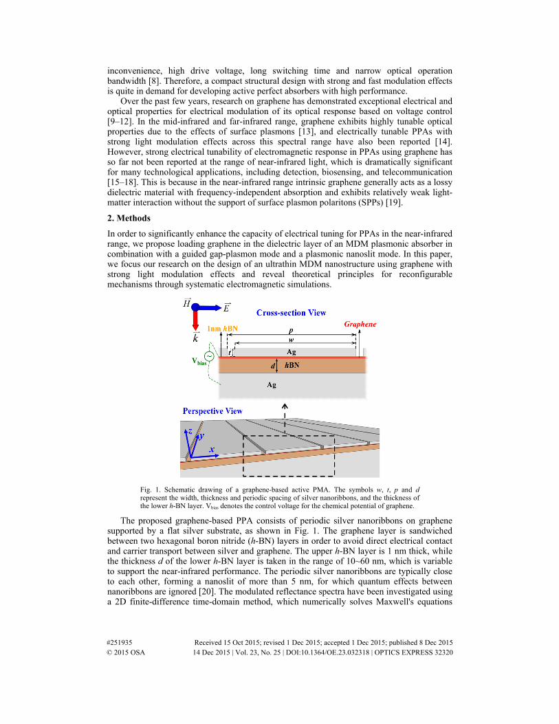
Fig. 1. Schematic drawing of a graphene-based active PMA. The symbols w, t, p and d represent the width, thickness and periodic spacing of silver nanoribbons, and the thickness of the lower h-BN layer. Vbias denotes the control voltage for the chemical potential of graphene.
The proposed graphene-based PPA consists of periodic silver nanoribbons on graphene supported by a flat silver substrate, as shown in Fig. 1. The graphene layer is sandwiched between two hexagonal boron nitride (h-BN) layers in order to avoid direct electrical contact and carrier transport between silver and graphene. The upper h-BN layer is 1 nm thick, while the thickness d of the lower h-BN layer is taken in the range of 10~60 nm, which is variable to support the near-infrared performance. The periodic silver nanoribbons are typically close to each other, forming a nanoslit of more than 5 nm, for which quantum effects between nanoribbons are ignored [20]. The modulated reflectance spectra have been investigated using a 2D finite-difference time-domain method, which numerically solves Maxwell's equations
#251935 Received 15 Oct 2015; revised 1 Dec 2015; accepted 1 Dec 2015; published 8 Dec 2015 © 2015 OSA 14 Dec 2015 | Vol. 23, No. 25 | DOI:10.1364/OE.23.032318 | OPTICS EXPRESS 32320
under Floquet boundary conditions and open boundary conditions (perfect matched layers). The optical constants of silver and lossless h-BN are taken from literature [21, 22], and the non-uniform discrete mesh is applied for all simulations. In view of the structural polarization characteristics, TM wave illumination is used for the study. This work is based on simplified 2D electromagnetic simulations for metallic nanoribbons with an infinite length, but the research achievements can be also extended to applications of PPAs using metallic nanoparticles.
Since the interaction between light and graphene originates from carrier transport on the atomic thin film, we assume that graphene is an anisotropic dispersive dielectric material with an effective relative permittivity tensor E as
( ) 0 0
0 ( ) 0
0 0
xx
yy
zz
E
ε ωε ω
ε
=
(1)
where ω is the angular frequency of light, εzz is assumed as an out-of-plane component of graphene with a constant value of 9.0 [23], εxx(ω) and εyy(ω) are in-plane components of permittivity, which can be represented by the surface conductivity of graphene σ as
0( ) ( ) ( )in xx yy iσε ω ε ω ε ω εω
= = = +Δ
(2)
where ε0 is the permittivity of vacuum, and the thickness of graphene ∆ is assumed as 0.5 nm [24]. The surface conductivity of graphene σ can be calculated by the Kubo formula as below [25,26],
intra inter( , , ,T)c Гσ ω μ σ σ+= (3)
2
intra 2 0
,T( , ) ( , )
( 2
T
)
,d c d cf fjed
j Г
ξ μ ξ μσ ξ ξξ ξπ ω
∞ ∂ ∂ − = − ∂ ∂−
(4)
2
inter 2 2 20
( , ) ( , )( 2 )
( 2 )
T
)
T
4
,
( /
,d c d cf fje j Гd
j Г
ξ μ ξ μωσ ξπ ω ξ
∞ − −−= −− −
(5)
( ) ( )/ 1, , ( 1)c Bkd
Tcf T e ξ μξ μ − −= + (6)
where σintra and σinter are originated from the intraband and interband transition, respectively, fd(ξ, μc, T) is the Fermi-Dirac distribution function, ħ is the reduced Planck constant, e is the electron charge, μc is the chemical potential, T is Kelvin temperature, Г is the scattering rate, kB is the Boltzmann constant, and ξ is the energy of electrons. For the physical model of graphene, we assume the effects of optical saturation and non-linear response are ignored. Based on the experimental work from Zhang et al. [27], Г is taken as 16.67 ps−1, and room temperature T = 300 K is assumed for all simulations. Therefore, the value of σ mainly depends on μc and ω, and the value of μc ranging from 0.1 eV to1.0 eV in the near-infrared regime is investigated in this study [28].
#251935 Received 15 Oct 2015; revised 1 Dec 2015; accepted 1 Dec 2015; published 8 Dec 2015 © 2015 OSA 14 Dec 2015 | Vol. 23, No. 25 | DOI:10.1364/OE.23.032318 | OPTICS EXPRESS 32321
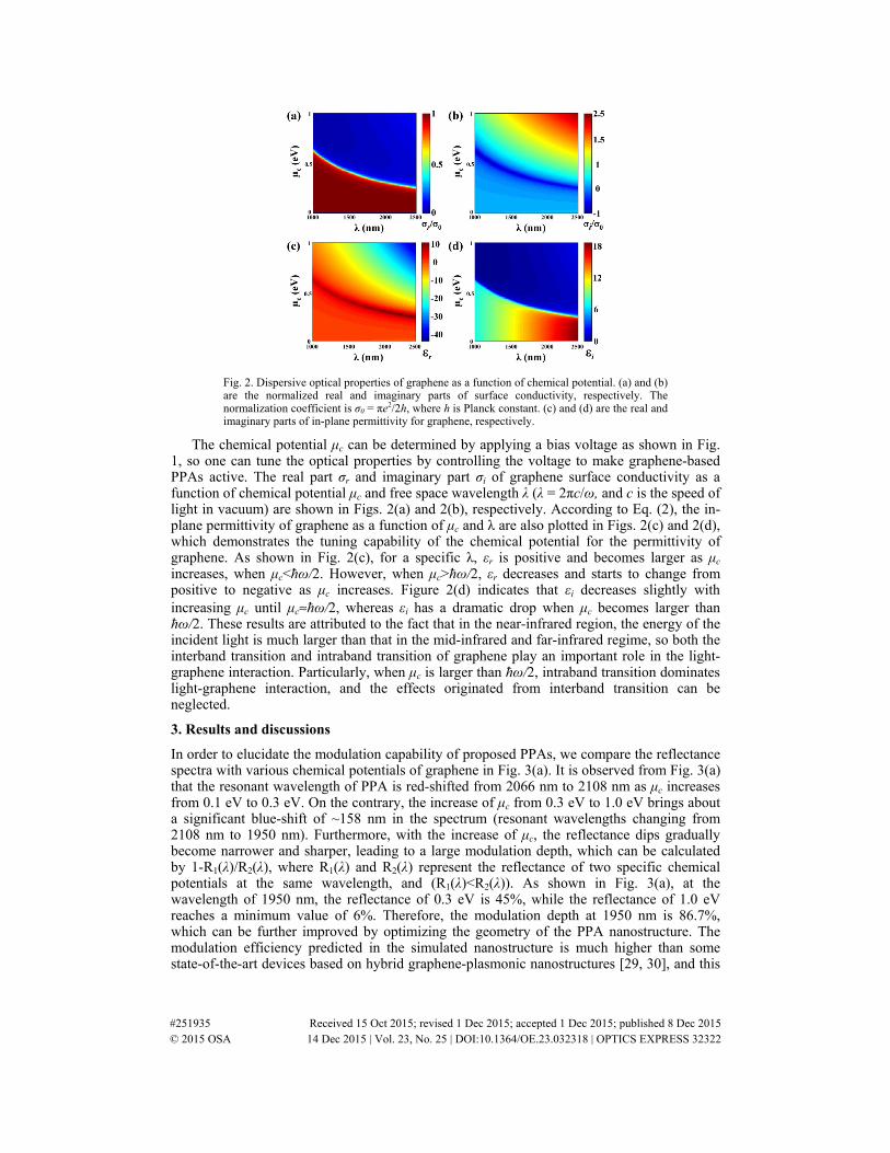
Fig. 2. Dispersive optical properties of graphene as a function of chemical potential. (a) and (b) are the normalized real and imaginary parts of surface conductivity, respectively. The normalization coefficient is σ0 = πe2/2h, where h is Planck constant. (c) and (d) are the real and imaginary parts of in-plane permittivity for graphene, respectively.
The chemical potential μc can be determined by applying a bias voltage as shown in Fig. 1, so one can tune the optical properties by controlling the voltage to make graphene-based PPAs active. The real part σr and imaginary part σi of graphene surface conductivity as a function of chemical potential μc and free space wavelength λ (λ = 2πc/ω, and c is the speed of light in vacuum) are shown in Figs. 2(a) and 2(b), respectively. According to Eq. (2), the in-plane permittivity of graphene as a function of μc and λ are also plotted in Figs. 2(c) and 2(d), which demonstrates the tuning capability of the chemical potential for the permittivity of graphene. As shown in Fig. 2(c), for a specific λ, εr is positive and becomes larger as μc increases, when μc<ħω/2. However, when μc>ħω/2, εr decreases and starts to change from positive to negative as μc increases. Figure 2(d) indicates that εi decreases slightly with increasing μc until μc≈ħω/2, whereas εi has a dramatic drop when μc becomes larger than ħω/2. These results are attributed to the fact that in the near-infrared region, the energy of the incident light is much larger than that in the mid-infrared and far-infrared regime, so both the interband transition and intraband transition of graphene play an important role in the light-graphene interaction. Particularly, when μc is larger than ħω/2, intraband transition dominates light-graphene interaction, and the effects originated from interband transition can be neglected.
3. Results and discussions
In order to elucidate the modulation capability of proposed PPAs, we compare the reflectance spectra with various chemical potentials of graphene in Fig. 3(a). It is observed from Fig. 3(a) that the resonant wavelength of PPA is red-shifted from 2066 nm to 2108 nm as μc increases from 0.1 eV to 0.3 eV. On the contrary, the increase of μc from 0.3 eV to 1.0 eV brings about a significant blue-shift of ~158 nm in the spectrum (resonant wavelengths changing from 2108 nm to 1950 nm). Furthermore, with the increase of μc, the reflectance dips gradually become narrower and sharper, leading to a large modulation depth, which can be calculated by 1-R1(λ)/R2(λ), where R1(λ) and R2(λ) represent the reflectance of two specific chemical potentials at the same wavelength, and (R1(λ)<R2(λ)). As shown in Fig. 3(a), at the wavelength of 1950 nm, the reflectance of 0.3 eV is 45%, while the reflectance of 1.0 eV reaches a minimum value of 6%. Therefore, the modulation depth at 1950 nm is 86.7%, which can be further improved by optimizing the geometry of the PPA nanostructure. The modulation efficiency predicted in the simulated nanostructure is much higher than some state-of-the-art devices based on hybrid graphene-plasmonic nanostructures [29, 30], and this
#251935 Received 15 Oct 2015; revised 1 Dec 2015; accepted 1 Dec 2015; published 8 Dec 2015 © 2015 OSA 14 Dec 2015 | Vol. 23, No. 25 | DOI:10.1364/OE.23.032318 | OPTICS EXPRESS 32322
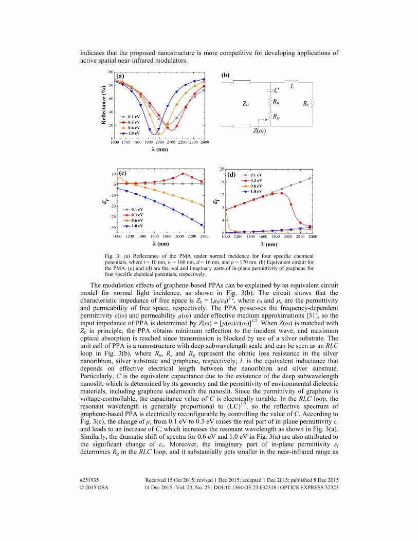
indicates that the proposed nanostructure is more competitive for developing applications of active spatial near-infrared modulators.
Fig. 3. (a) Reflectance of the PMA under normal incidence for four specific chemical potentials, where t = 10 nm, w = 160 nm, d = 16 nm, and p = 170 nm. (b) Equivalent circuit for the PMA. (c) and (d) are the real and imaginary parts of in-plane permittivity of graphene for four specific chemical potentials, respectively.
The modulation effects of graphene-based PPAs can be explained by an equivalent circuit model for normal light incidence, as shown in Fig. 3(b). The circuit shows that the characteristic impedance of free space is Z0 = (µ0/ε0)
1/2, where ε0 and µ0 are the permittivity and permeability of free space, respectively. The PPA possesses the frequency-dependent permittivity ε(ω) and permeability µ(ω) under effective medium approximations [31], so the input impedance of PPA is determined by Z(ω) = [µ(ω)/ε(ω)]1/2. When Z(ω) is matched with Z0 in principle, the PPA obtains minimum reflection to the incident wave, and maximum optical absorption is reached since transmission is blocked by use of a silver substrate. The unit cell of PPA is a nanostructure with deep subwavelength scale and can be seen as an RLC loop in Fig. 3(b), where Rn, Rs and Rg represent the ohmic loss resistance in the silver nanoribbon, silver substrate and graphene, respectively; L is the equivalent inductance that depends on effective electrical length between the nanoribbon and silver substrate. Particularly, C is the equivalent capacitance due to the existence of the deep subwavelength nanoslit, which is determined by its geometry and the permittivity of environmental dielectric materials, including graphene underneath the nanoslit. Since the permittivity of graphene is voltage-controllable, the capacitance value of C is electrically tunable. In the RLC loop, the resonant wavelength is generally proportional to (LC)1/2, so the reflective spectrum of graphene-based PPA is electrically reconfigurable by controlling the value of C. According to Fig. 3(c), the change of μc from 0.1 eV to 0.3 eV raises the real part of in-plane permittivity εr and leads to an increase of C, which increases the resonant wavelength as shown in Fig. 3(a). Similarly, the dramatic shift of spectra for 0.6 eV and 1.0 eV in Fig. 3(a) are also attributed to the significant change of εr. Moreover, the imaginary part of in-plane permittivity εi determines Rg in the RLC loop, and it substantially gets smaller in the near-infrared range as
#251935 Received 15 Oct 2015; revised 1 Dec 2015; accepted 1 Dec 2015; published 8 Dec 2015 © 2015 OSA 14 Dec 2015 | Vol. 23, No. 25 | DOI:10.1364/OE.23.032318 | OPTICS EXPRESS 32323

μc increases from 0.1 eV to 1.0 eV as shown in Fig. 3(d), which promotes the quality factor of reflectance spectra and makes the spectral dips tend to be narrower and sharper as shown in Fig. 3(a).
Fig. 4. Electromagnetic field distributions under normal incident light for specific μc and λ, where t = 10 nm, w = 160 nm, d = 16 nm and p = 170 nm, and the white lines sketch the profile of different materials. (a), (b) and (c) denote electric field intensity. (d), (e) and (f) are magnetic field intensity.
To obtain further insight into the physical origin of reflectance modulation, we discuss the electromagnetic field distributions of two specific μc, as shown in Fig. 4. Analogous to other PPAs based on MDM structures [32], the suppressed reflectance is attributed to matching of the wave impedance between vacuum and the artificial structure, which is further derived from the superposition of inverse optical fields that are induced by electric dipole (Figs. 4(a)-4(c)) and magnetic dipole (Figs. 4(d)-4(f)) excited by the incident wave. The incident fields are trapped between the silver nanoribbon and the silver substrate as the guided gap-plasmon mode and further induce the effects of resonant absorption, which has been systematically demonstrated in our previous work [33]. Next, we focus on investigating electromagnetic effects of the nanoslit based on field analysis. In the proposed nanostructure, neighboring silver nanoribbons are extremely close (~10 nm) to each other, the evanescent field scattered by one nanoribbon is considerably strong in the vicinity of the other nanoribbon compared to the exciting field, and this leads to the intense coupling of scattered field from each nanoribbon, so that the electric field is dramatically enhanced and concentrated surrounding the edges of the nanoribbons and inside the nanoslit, as shown in Figs. 4(a)-4(c).
The high confinement of electric field energy density in the deep subwavelength scale can be further attributed to the plasmonic nanoslit mode, in which there is a resonant excitation of the fundamental field-symmetric SPP mode supported by the truncated metal-slit-metal plasmonic waveguide [34, 35]. Graphene is closely located underneath the nanoslit, so changing the optical properties of graphene by chemical potential μc can significantly tune the coupling effects between neighboring silver nanoribbons, which influences the resonant wavelength of PPAs, as shown in Figs. 4(a)-4(c). When μc = 0.3 eV, graphene acts as a lossy dielectric material and exhibits relatively weak light-graphene interaction as shown in Fig. 4(a). At λ = 1950 nm, when μc is switched to 1.0 eV from 0.3 eV, εr of graphene changes from positive to negative, and εi of graphene becomes much smaller, which provides conditions that satisfy the generation of SPPs and enhance light-graphene interaction as shown in Fig. 4(c). The interaction enhancement mainly strengthens the in-plane electric field coupling and significantly influences the resonant wavelength, and the effects of SPPs on graphene influence the direction of magnetic field (as shown in Fig. 4(f)) much more slightly, compared with the electric field in Fig. 4(c). This is because non-magnetic graphene has an
#251935 Received 15 Oct 2015; revised 1 Dec 2015; accepted 1 Dec 2015; published 8 Dec 2015 © 2015 OSA 14 Dec 2015 | Vol. 23, No. 25 | DOI:10.1364/OE.23.032318 | OPTICS EXPRESS 32324
ultrathin volume in the dielectric layer and its out-of-plane permeability is always constant. The electromagnetic simulation results imply that the strong reconfigurable effects of PPA mainly depends on the electrical tuning on the part of graphene underneath the nanoslit; nevertheless, only tuning μc for the part of graphene right under the silver nanoribbon influence the optical properties of PPAs very slightly. Therefore, the design for the nanoslit plays a critical role in enhancing the modulation effects of graphene-based PPAs.
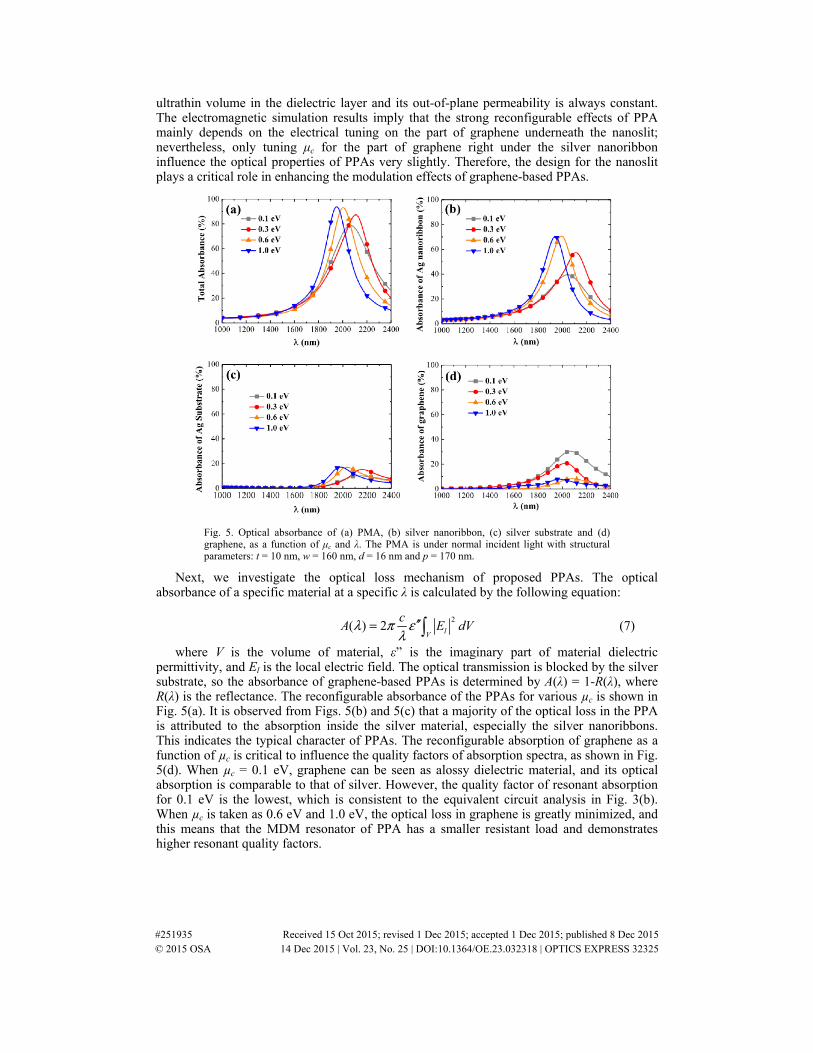
Fig. 5. Optical absorbance of (a) PMA, (b) silver nanoribbon, (c) silver substrate and (d) graphene, as a function of μc and λ. The PMA is under normal incident light with structural parameters: t = 10 nm, w = 160 nm, d = 16 nm and p = 170 nm.
Next, we investigate the optical loss mechanism of proposed PPAs. The optical absorbance of a specific material at a specific λ is calculated by the following equation:
2
( ) 2 lV
cA E dVλ π ε
λ′′= (7)
where V is the volume of material, ε” is the imaginary part of material dielectric permittivity, and El is the local electric field. The optical transmission is blocked by the silver substrate, so the absorbance of graphene-based PPAs is determined by A(λ) = 1-R(λ), where R(λ) is the reflectance. The reconfigurable absorbance of the PPAs for various µc is shown in Fig. 5(a). It is observed from Figs. 5(b) and 5(c) that a majority of the optical loss in the PPA is attributed to the absorption inside the silver material, especially the silver nanoribbons. This indicates the typical character of PPAs. The reconfigurable absorption of graphene as a function of µc is critical to influence the quality factors of absorption spectra, as shown in Fig. 5(d). When µc = 0.1 eV, graphene can be seen as alossy dielectric material, and its optical absorption is comparable to that of silver. However, the quality factor of resonant absorption for 0.1 eV is the lowest, which is consistent to the equivalent circuit analysis in Fig. 3(b). When µc is taken as 0.6 eV and 1.0 eV, the optical loss in graphene is greatly minimized, and this means that the MDM resonator of PPA has a smaller resistant load and demonstrates higher resonant quality factors.
#251935 Received 15 Oct 2015; revised 1 Dec 2015; accepted 1 Dec 2015; published 8 Dec 2015 © 2015 OSA 14 Dec 2015 | Vol. 23, No. 25 | DOI:10.1364/OE.23.032318 | OPTICS EXPRESS 32325
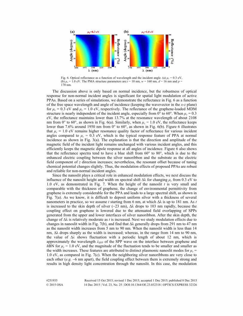
Fig. 6. Optical reflectance as a function of wavelength and the incident angle. (a) μc = 0.3 eV, (b) μc = 1.0 eV. The PMA structure parameters are:t = 10 nm, w = 160 nm, d = 16 nm and p = 170 nm.
The discussion above is only based on normal incidence, but the robustness of optical response for non-normal incident angles is significant for spatial light modulation of active PPAs. Based on a series of simulations, we demonstrate the reflectance in Fig. 6 as a function of the free space wavelength and angle of incidence (keeping the wavevector in the x-z plane) for μc = 0.3 eV and μc = 1.0 eV, respectively. The reflectance of the graphene-loaded MDM structure is nearly independent of the incident angle, especially from 0° to 60°. When μc = 0.3 eV, the reflectance maintains lower than 13.7% at the resonance wavelength of about 2108 nm from 0° to 60°, as shown in Fig. 6(a). Similarly, when μc = 1.0 eV, the reflectance keeps lower than 7.6% around 1950 nm from 0° to 60°, as shown in Fig. 6(b). Figure 6 illustrates that μc = 1.0 eV remains higher resonance quality factor of reflectance for various incident angles compared to μc = 0.3 eV, which is the typical response feature of PPA at normal incidence as shown in Fig. 3(a). The explanation is that the direction and amplitude of the magnetic field of the incident light remains unchanged with various incident angles, and this efficiently keeps the magnetic dipole response at all angles of incidence. Figure 6 also shows that the reflectance spectra tend to have a blue shift from 60° to 80°, which is due to the enhanced electric coupling between the silver nanoribbon and the substrate as the electric field component of z direction increases; nevertheless, the resonant offset because of tuning chemical potential changes slightly. Thus, the modulation effects of proposed PPAs are robust and reliable for non-normal incident angles.
Since the nanoslit plays a critical role in enhanced modulation effects, we next discuss the influence of the nanoslit height and width on spectral shift ∆λ for changing μc from 0.3 eV to 1.0 eV, as demonstrated in Fig. 7. When the height of the nanoslit t is very small and comparable with the thickness of graphene, the change of environmental permittivity from graphene is extremely considerable for the PPA and leads to a large spectral shift, as shown in Fig. 7(a). As we know, it is difficult to deposit uniform silver with a thickness of several nanometers in practice, so we assume t starting from 6 nm, at which ∆λ is up to 181 nm. As t is increased to the skin depth of silver (~23 nm), ∆λ drops to 103 nm rapidly, because the coupling effect on graphene is lowered due to the attenuated field overlapping of SPPs generated from the upper and lower interfaces of silver nanoribbon. After the skin depth, the change of ∆λ is relatively moderate as t is increased. Next we study modulation effects due to changes in nanoslit width in Fig. 7(b), and find that ∆λ generally drops from 291 nm to 47 nm as the nanoslit width increases from 5 nm to 90 nm. When the nanoslit width is less than 14 nm, ∆λ drops sharply as the width is increased; whereas, in the range from 14 nm to 90 nm, the value of ∆λ shows fluctuation with a periodic length of about 12 nm, which is approximately the wavelength λSPP of the SPP wave on the interface between graphene and hBN for μc = 1.0 eV, and the magnitude of the fluctuation tends to be smaller and smaller as the width increases. These features are attributed to distinct plasmonic nanoslit modes for μc = 1.0 eV, as compared in Fig. 7(c). When the neighboring silver nanoribbons are very close to each other (e.g. ~6 nm apart), the field coupling effect between them is extremely strong and results in high density light concentration through the nanoslit. In this case, the modulation
#251935 Received 15 Oct 2015; revised 1 Dec 2015; accepted 1 Dec 2015; published 8 Dec 2015 © 2015 OSA 14 Dec 2015 | Vol. 23, No. 25 | DOI:10.1364/OE.23.032318 | OPTICS EXPRESS 32326
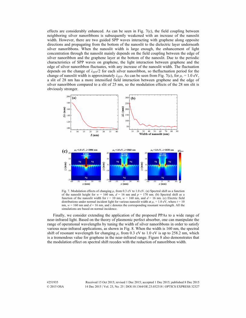
effects are considerably enhanced. As can be seen in Fig. 7(c), the field coupling between neighboring silver nanoribbons is subsequently weakened with an increase of the nanoslit width. However, there are two guided SPP waves interacting with graphene along opposite directions and propagating from the bottom of the nanoslit to the dielectric layer underneath silver nanoribbons. When the nanoslit width is large enough, the enhancement of light concentration through the nanoslit mainly depends on the field coupling between the edge of silver nanoribbon and the graphene layer at the bottom of the nanoslit. Due to the periodic characteristics of SPP waves on graphene, the light interaction between graphene and the edge of silver nanoribbon fluctuates, with any increase of the nanoslit width. The fluctuation depends on the change of λSPP/2 for each silver nanoribbon, so thefluctuation period for the change of nanoslit width is approximately λSPP. As can be seen from Fig. 7(c), for μc = 1.0 eV, a slit of 28 nm has a more intensified field interaction between graphene and the edge of silver nanoribbon compared to a slit of 25 nm, so the modulation effects of the 28 nm slit is obviously stronger.
Fig. 7. Modulation effects of changing μc from 0.3 eV to 1.0 eV. (a) Spectral shift as a function of the nanoslit height for w = 160 nm, d = 16 nm and p = 170 nm. (b) Spectral shift as a function of the nanoslit width for t = 10 nm, w = 160 nm, and d = 16 nm. (c) Electric field distributions under normal incident light for various nanoslit width at μc = 1.0 eV, where t = 10 nm, w = 160 nm and d = 16 nm, and λ denotes the corresponding resonant wavelength. All the simulations are based on normal incidence.
Finally, we consider extending the application of the proposed PPAs to a wide range of near-infrared light. Based on the theory of plasmonic perfect absorber, one can manipulate the range of operational wavelengths by tuning the width of silver nanoribbons in order to satisfy various near-infrared applications, as shown in Fig. 8. When the width is 160 nm, the spectral shift of resonant wavelength for changing μc from 0.3 eV to 1.0 eV is up to 258.2 nm, which is a tremendous value for graphene in the near-infrared range. Figure 8 also demonstrates that the modulation effect on spectral shift recedes with the reduction of nanoribbon width.
#251935 Received 15 Oct 2015; revised 1 Dec 2015; accepted 1 Dec 2015; published 8 Dec 2015 © 2015 OSA 14 Dec 2015 | Vol. 23, No. 25 | DOI:10.1364/OE.23.032318 | OPTICS EXPRESS 32327
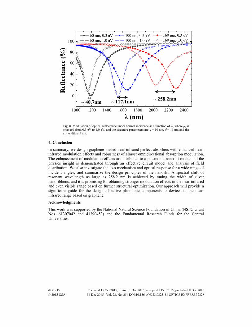
Fig. 8. Modulation of optical reflectance under normal incidence as a function of w, where μc is changed from 0.3 eV to 1.0 eV, and the structure parameters are: t = 10 nm, d = 16 nm and the slit width is 5 nm.
4. Conclusion
In summary, we design graphene-loaded near-infrared perfect absorbers with enhanced near-infrared modulation effects and robustness of almost omnidirectional absorption modulation. The enhancement of modulation effects are attributed to a plasmonic nanoslit mode, and the physics insight is demonstrated through an effective circuit model and analysis of field distribution. We also investigate the loss mechanism and optical response for a wide range of incident angles, and summarize the design principles of the nanoslit. A spectral shift of resonant wavelength as large as 258.2 nm is achieved by tuning the width of silver nanoribbons, and it is promising for obtaining stronger modulation effects in the near-infrared and even visible range based on further structural optimization. Our approach will provide a significant guide for the design of active plasmonic components or devices in the near-infrared range based on graphene.
Acknowledgments
This work was supported by the National Natural Science Foundation of China (NSFC Grant Nos. 61307042 and 41390453) and the Fundamental Research Funds for the Central Universities.
#251935 Received 15 Oct 2015; revised 1 Dec 2015; accepted 1 Dec 2015; published 8 Dec 2015 © 2015 OSA 14 Dec 2015 | Vol. 23, No. 25 | DOI:10.1364/OE.23.032318 | OPTICS EXPRESS 32328