Engineering Responsive, Tunable, and Multifunctional Composites
117
Engineering Responsive, Tunable, and Multifunctional Composites by Terry C. Shyu A dissertation submitted in partial fulfillment of the requirements for the degree of Doctor of Philosophy (Materials Science and Engineering) in The University of Michigan 2016 Doctoral Committee: Professor Nicholas A. Kotov, Chair Professor Sharon C. Glotzer Associate Professor Peicheng Ku Associate Professor Max Shtein
Transcript of Engineering Responsive, Tunable, and Multifunctional Composites

Engineering Responsive, Tunable, andMultifunctional Composites
by
Terry C. Shyu
A dissertation submitted in partial fulfillmentof the requirements for the degree of
Doctor of Philosophy(Materials Science and Engineering)
in The University of Michigan2016
Doctoral Committee:
Professor Nicholas A. Kotov, ChairProfessor Sharon C. GlotzerAssociate Professor Peicheng KuAssociate Professor Max Shtein

c⃝ Terry C. Shyu 2016
All Rights Reserved

To my grandfather
ii

ACKNOWLEDGEMENTS
The first time I spoke to Prof. Nicholas Kotov, he asked me my reasons for
pursuing a doctoral degree, and what I wanted out of my experience here. I am
not sure whether either of us remembers what my answer was, but the one thing
I am certain of is that under his guidance I have gained much more than what I
imagined that day. I am very fortunate and grateful for his support, encouragement,
and mentorship throughout these years. Likewise, I would like to thank my Ph.D.
committee, Prof. Sharon Glotzer, Prof. P. C. Ku, and Prof. Max Shtein, for their
valuable contribution, wholehearted support, and the vision that set our project in
motion. I would also like to thank especially Prof. Max Shtein, for challenging me to
think about our responsibility to contribute to science in however small ways.
I thank all the Folders as collaborators and friends. I hope each of them
had enjoyed our work as much as I did. These include Pablo Damasceno, Paul Dodd,
Matt Shlian, Aaron Lamoureux, Chi-Wei Chien, and many others who have moved on
since we started the Folders group. This work would not have been possible without
the support of the National Science Foundation, the I-Corps Program, Rackham
Graduate School, the Electron and Microbeam Analysis Laboratory (EMAL) and
the Lurie Nanofabrication Facility (LNF).
I am indebted to Prof. James Barber, Prof. John Foster, Dr. Huanan Zhang,
iii

Dr. Bongjun Yeom, Dr. Kyounggun Lee, Dr. Christine Andres, Dr. Jian Zhu, Siu-
On Tung, and Joong Hwan Bahng, for their scientific discussions that influenced this
work; Dr. Ralph Yang, Dr. Robert Hower, Dr. Pilar Herrera-Fierro, Dr. Nadine
Wang, and Dr. Katherine Beach for the mentorship and technical support; Harald,
a true engineer in every sense of the word, for his enthusiasm that permeates every-
thing he touches; Yichun, Harish, Steven, Jennifer, Carlos, and Julie, for lending me
perspective and food to nourish the body; and Albert, for encouraging me to build
substance. Lastly, I am thankful for my family for allowing me the freedom to pursue
anything that strikes my fancy and conversations on the meaning of everything.
iv

TABLE OF CONTENTS
DEDICATION . . . . . . . . . . . . . . . . . . . . . . . . . . . . . . . . . . ii
ACKNOWLEDGEMENTS . . . . . . . . . . . . . . . . . . . . . . . . . . iii
LIST OF FIGURES . . . . . . . . . . . . . . . . . . . . . . . . . . . . . . . ix
ABSTRACT . . . . . . . . . . . . . . . . . . . . . . . . . . . . . . . . . . . xiii
CHAPTER
I. Introduction . . . . . . . . . . . . . . . . . . . . . . . . . . . . . . 1
1.1 A Brief History of Engineering Origami . . . . . . . . . . . . 1
1.1.1 Deployability and Foldability . . . . . . . . . . . . . 4
1.1.2 Toward 3 Dimensionality . . . . . . . . . . . . . . . 6
1.1.3 Self-Assembled Molecular Origami . . . . . . . . . . 11
v
1.1.4 Novel 2D Materials . . . . . . . . . . . . . . . . . . 13
1.2 Responsive and Reconfigurable Nanocomposites . . . . . . . . 15
1.3 Focus of the Thesis . . . . . . . . . . . . . . . . . . . . . . . 16
1.4 Organization of the Thesis . . . . . . . . . . . . . . . . . . . 17
II. Methods and Techniques . . . . . . . . . . . . . . . . . . . . . . . 19
2.1 Introduction . . . . . . . . . . . . . . . . . . . . . . . . . . . 19
2.2 Microscopy and Imaging . . . . . . . . . . . . . . . . . . . . . 19
2.3 Mechanics . . . . . . . . . . . . . . . . . . . . . . . . . . . . . 21
2.3.1 Stress-Strain Behavior . . . . . . . . . . . . . . . . . 21
2.3.2 Finite Element Modeling . . . . . . . . . . . . . . . 23
2.4 Fabrication Techniques . . . . . . . . . . . . . . . . . . . . . 25
2.4.1 Thin Films . . . . . . . . . . . . . . . . . . . . . . . 25
2.4.2 Photolithography . . . . . . . . . . . . . . . . . . . 28
2.4.3 Etching . . . . . . . . . . . . . . . . . . . . . . . . . 30
2.4.4 Inkjet Printing and Additive Manufacturing . . . . 31
III. Responsive Inkjet Printed Layer-by-Layer Assembled Films 33
vi

3.1 Inkjet Patterning of Nanocomposites . . . . . . . . . . . . . . 34
3.2 Contact Angle and Wettability . . . . . . . . . . . . . . . . . 38
3.2.1 Nanopillar arrays . . . . . . . . . . . . . . . . . . . 41
3.2.2 Local Contact Angle Modification Using Inkjet LBL 45
3.3 Overt and Covert Images . . . . . . . . . . . . . . . . . . . . 47
3.4 Conclusion . . . . . . . . . . . . . . . . . . . . . . . . . . . . 48
IV. Engineering Properties with Kirigami Nanocomposite . . . . 50
4.1 Background . . . . . . . . . . . . . . . . . . . . . . . . . . . . 51
4.2 The Kirigami Approach . . . . . . . . . . . . . . . . . . . . . 52
4.3 Mechanical Behavior . . . . . . . . . . . . . . . . . . . . . . . 54
4.4 Unit Cell and Buckling . . . . . . . . . . . . . . . . . . . . . 56
4.5 Control of Deformation . . . . . . . . . . . . . . . . . . . . . 59
4.6 Strain-Conductivity Relationship . . . . . . . . . . . . . . . . 63
4.7 Conclusion . . . . . . . . . . . . . . . . . . . . . . . . . . . . 69
V. Tunable Kirigami . . . . . . . . . . . . . . . . . . . . . . . . . . . 71
5.1 Background . . . . . . . . . . . . . . . . . . . . . . . . . . . . 72
vii

5.2 Experimental Method . . . . . . . . . . . . . . . . . . . . . . 73
5.3 Strain-Tunable Plasma Parameters . . . . . . . . . . . . . . . 74
5.4 Conclusion . . . . . . . . . . . . . . . . . . . . . . . . . . . . 77
VI. Summary and Future Directions . . . . . . . . . . . . . . . . . . 79
6.1 Time Scale . . . . . . . . . . . . . . . . . . . . . . . . . . . . 80
6.2 Length Scale . . . . . . . . . . . . . . . . . . . . . . . . . . . 81
6.3 Design of Deformation . . . . . . . . . . . . . . . . . . . . . . 83
BIBLIOGRAPHY . . . . . . . . . . . . . . . . . . . . . . . . . . . . . . . . 86
viii
LIST OF FIGURES
Figure
1.1 The art of paper folding, origami, started from the first description ofa paper crane and since then evolved into more complicated structures. 2
1.2 The first demonstration of a folding pattern used in the context ofengineering, where the folding pattern mimics the natural bucklingshape of a cylindrical shell. . . . . . . . . . . . . . . . . . . . . . . . 3
1.3 The mechanics of the Miura-ori is determined by a small set of foldingangles. . . . . . . . . . . . . . . . . . . . . . . . . . . . . . . . . . . 4
1.4 Research effort in engineering origami focuses on using 2D patterningtechnique to generate 3D structures on small length scales. . . . . . 11
1.5 DNA origami as a bottom-up nanofabrication technique. . . . . . . 12
2.1 Typical LBL assembly process. . . . . . . . . . . . . . . . . . . . . . 27
2.2 Typical lithographic steps. . . . . . . . . . . . . . . . . . . . . . . . 29
ix

3.1 The molecular structures of cationic poly(diallyldimethylammoniumchloride) (PDDA) and anionic poly(sodium 4-styrenesulfonate) (PSS). 37
3.2 Schematic of a an inkjet printing assisted LBL process. . . . . . . . 37
3.3 Schematic of a droplet residing on a solid surface and energy balance,depicting the interface tensions and the contact angle θ. . . . . . . . 39
3.4 Schematic steps to create the nanopillar mold and the subsequentnanomolding. . . . . . . . . . . . . . . . . . . . . . . . . . . . . . . 42
3.5 SEM images of the nanopillars after rubbing cycles. . . . . . . . . . 43
3.6 Contact angle dependence on surface modification and mechanicalabrasion with corresponding SEM images. . . . . . . . . . . . . . . 44
3.7 Overt and covert images printed on nanopillar arrays using inkjetLBL deposition. . . . . . . . . . . . . . . . . . . . . . . . . . . . . 47
4.1 Microscale kirigami patterns. . . . . . . . . . . . . . . . . . . . . . . 53
4.2 Typical stress-strain response for kirigami patterned sheets. . . . . 55
4.3 Schematics showing force analysis approximating kirigami struts asbeams. . . . . . . . . . . . . . . . . . . . . . . . . . . . . . . . . . . 56
x

4.4 Photographs of paper samples, showing that as the sample extendsunder uniaxial tension, the system chooses the favorable configurationby bending out of plane. . . . . . . . . . . . . . . . . . . . . . . . . 59
4.5 SEM showing the morphology of the sheets. . . . . . . . . . . . . . 61
4.6 Experimental and FEM-calculated stress-strain curves for macroscalekirigami sheets with variable unit-cell parameters. . . . . . . . . . . 62
4.7 Stress concentration visualization in FEM. . . . . . . . . . . . . . . 63
4.8 Blunting the cut edge in the form of a circle at the edge of the cutscan further distribute the stress at each cut edge. . . . . . . . . . . 64
4.9 SEM images showing the microstructure of CNT nanocomposite on(a) paper, fabricated by vacuum infiltration, and (b) on parylene,fabricated by LBL. . . . . . . . . . . . . . . . . . . . . . . . . . . . 65
4.10 Schematics of the custom-made plasma chamber. . . . . . . . . . . . 67
4.11 Strain-invariant conductance on CNT nanocomposites as an elec-trode. . . . . . . . . . . . . . . . . . . . . . . . . . . . . . . . . . . 68
4.12 Cyclic loading data for the nanocomposite paper and polyimide,showing elastic energy recovery. . . . . . . . . . . . . . . . . . . . . 70
5.1 Qualitative data showing stress-tunable plasma properties. . . . . . 75
xi

5.2 Quantitative data showing stress-tunable plasma properties. . . . . 76
5.3 Rotating kirigami structures with out-of-plane twists. . . . . . . . . 78
xii

ABSTRACT
Engineering Responsive, Tunable, and Multifunctional Composites
by
Terry Shyu
Chair: Prof. Nicholas A. Kotov
In recent years, engineering origami, inspired by paper art, is gaining traction in the
study of reconfigurability because of its robustness as a mechanical system. These
mechanical systems enable functional properties and can be extended to multiple
length scales for a range of applications, including biomedicine, sensing, and smart
materials. Here we explore two key strategies to enable new materials designs for
responsiveness and tunable properties. The first deals with how we can combine
desirable properties onto a single material, and the second deals with how the material
is arranged spatially.
In this work, we focus on a layer-by-layer (LBL) assembled composite tech-
nique, which provides nanoscale control and mechanically robust composites suitable
for reversible responsive systems. In the first part of the work inkjet printing is used
produce these composites rapidly and to dictate spatial arrangement. We demon-
strate combining LBL with inkjet printing to introduce mechanical motion in a solid
xiii

nanocomposite system. Next we show using the same materials system and technique
to modulate surface properties by inkjet LBL on nanopillar arrays, and propose its
application in breath-activated authentication. The final part of the study focuses on
an extension of the origami approach to engineer stretchability in conductive compos-
ites. Kirigami, the art of paper cutting, controls the deformation within a composite,
which in turn gives us control over the strain-property relationship. The reconfigura-
bility enabled by kirigami can also be used for tunable applications. We show that the
combination of bottom-up and top-down patterning of composite materials demon-
strates new opportunities in materials engineering, and suggest future directions in
the field of engineering origami and kirigami.
xiv

CHAPTER I
Introduction
Materials science is the study of how we can expand the currently available
material properties in relation to its structure and processing. As part of my PhD
work, my projects involved cutting papers and printing Andy Warhol’s rendition of
Marilyn Monroe, which, at first glance, may seem more like a work in the arts than in
materials science. To really explain why these projects were relevant in the context of
creating new functional materials, we must first start by describing the idea of paper
art as a way to create mechanical systems, its application in various engineering fields,
and the intersection between materials and mechanics.
1.1 A Brief History of Engineering Origami
The manipulation of planar sheets into 3D objects dates back to the 1600s.
Since the invention of paper around 100 BC in ancient China, [1] which spread to
east Asia and to the west via the Silk Road, different cultures have used paper folding
for packaging and creative endeavors. The term “origami” (ori, fold; kami, paper) is
typically used to describe the art of paper folding because of the rich history associated
1

Figure 1.1: The art of paper folding, origami, started from the first description of apaper crane (left, made by the author) and since then evolved into morecomplicated structures (right, designed by Fumiaki Kawahata, fabricatedby Philip West.)
with the popular paper crane, first appearing in a book in 1797 [2] in Japan. The
art of origami has since become more and more sophisticated (Figure. 1.1), and
mathematical studies have been conceived to describe folding geometry. Origami in
its pure form does not allow cutting, whereas its variant “kirigami” involves cutting
of the sheet.
Using origami as a technique in science and engineering did not start until the
1970’s for its application in deployable structures. In a study in 1969, [3] Miura first
proposed a “pseudo-cylindrical concave polyhedral shell” that has a periodic folded
pattern. This pattern, as Miura described, was accidentally discovered by mimick-
ing the post-buckling configuration of a cylindrical shell structure, which makes the
structure collapsible. The folding pattern is later called the Miura-ori (Fig. 1.2), and
has since been used for deployable structures and engineer in-plane stiffness. [4] From
its beginning, it can already be seen that origami engineering can be used to couple
mechanical behavior and functionality. As a relatively new area of science, origami
has seen rapid development in science, engineering, and mathematics in the past few
2

Figure 1.2: The first demonstration of a folding pattern used in the context of engi-neering, where the folding pattern mimics the natural buckling shape ofa cylindrical shell. [3]
decades. The growing interest in origami engineering started in one aspect of engi-
neering as a way to create compact and deployable structures for easy deployment
for applications ranging from actuators to space exploration [5, 6]. Another fruitful
area of origami engineering is related to the growing interest in creating complex
geometries in three dimensions on smaller and smaller length scales. As micro- and
nanofabrication become more sophisticated, they are still inherently 2D techniques,
and origami provides a way to bring structures into the third dimension. [7, 8, 9]
Other emerging aspects of engineering origami also include the underlying physical
and mathematical rules for these foldable systems [10, 11, 12] and the nascent 2D
starting materials for reconfigurable applications. [13, 14, 15] These emerging areas
in origami engineering are discussed in the following sections.
3

Figure 1.3: The mechanics of the Miura-ori is determined by a small set of foldingangles. [16]
1.1.1 Deployability and Foldability
In the context of deployability, the Miura-ori pattern has been studied widely
for its intriguing mechanical properties, which are related to the geometry of the fold-
ing pattern. The folding pattern consists of two crease lengths that form a repeating
parallelogram pattern, a dihedral angle, an acute angle, and an angle that forms once
the pattern is folded, which is dependent on the degree of folding. In a 2009 study,
[16] Tachi laid out the flat-foldability condition for the Miura-ori pattern. In the
simplest form, this condition is dependent on 4 sector angles and 4 folding angles,
where one folding angle has to be negative, corresponding to a mountain fold and
the remaining three positive, corresponding to valley folds (Fig. 1.3). The crease
pattern that satisfies the flat-foldability condition has only one degree of freedom.
This property gives rise to Miura-ori’s deployability and negative Poisson’s ratio.
The kinematics of the Miura-ori pattern dictates that the Poissons ratio is
always negative in these patterns across the entire range of actuation as a function
of folding angle, or effectively, strain. Treating origami folded structures as rigid
panels connected to foldable and frictionless hinges, Demaine, [17] Schenk, [18] Lang,
4

[19, 20] and others have since studied the foldability for a given structure. The inverse
problem can also be solved: based on the desired final origami structure, it is possible
to derive the folding pattern. Based on just the kinematics of these folded patterns
and ignoring bending of the facets and fatigue at the creases, the deployability depends
only on the geometry and is length scale independent. The length scale independence
makes a convenient case for metamaterials, where the description of deformation can
be translated to any length scale. Silverberg et al [21] have exploited the properties
of Miura-ori and studied these systems as mechanical metamaterials, focusing on how
defects affect the mechanical behavior and guide elastic waves much like in a crystal.
As one can expect, however, it was also shown [22] that origami deployability is not
controlled by just the kinematics; in real systems thin sheets are also capable of
bending deformation, which also leads to mechanical bistability.
The idea of foldability is also relevant in the context of constructing 3 di-
mensional polyhedra from 2 dimensional nets. Theoretical work by Pendey et al [23]
points to an algorithmic approach to describe geometric rules that search for an easily
foldable path for a given polyhedron. For simple cases like the tetrahedron and the
cube, optimal nets are not hard to describe, but the number of possible nets grow very
quickly as the the number of faces increases. As it turns out, perhaps unsurprising to
origami artists, compactness and short folding pathways are essential considerations
in producing high yield polyhedra. This seemingly simple finding is important for
experimental demonstrations of self-folding polyhedra that followed.
5

1.1.2 Toward 3 Dimensionality
As mentioned previously, origami is of interest in creating complex geometries
in small dimensions. In the context of creating small structures, since Feynman’s
“plenty of room at the bottom” challenge in 1959, [24] miniaturization in electronics
has come a long way toward their physical limits. The first batch processed micro-
electromechanical systems (MEMS) device was produced shortly after. [25] Since
then, more complicated mechanical devices such as pressure sensors, actuators, and
micromotors have been made, adopting the batch fabrication processes used in silicon
integrated circuits. Formation of features relies on specialized etching techniques. [26]
These include bulk micromachining, surface micromachining, and the LIGA process
(German acronym for lithographie - lithography, galvanoformung - electroplating, and
abformung - molding). [27, 28] Most features, however, still lie within the wafer plane.
Microfabrication of electronics is inherently a 2D technology: photolithogra-
phy is employed, where patterns are optically transferred from a stencil mask to a
photosensitive material on a flat silicon wafer. The development of 2D patterning
techniques to enable integrated circuit miniaturization has also propelled its expan-
sion into shrinking three-dimensional mechanical structures. However, complex out-
of-plane geometries and those that allow for reversible 2D to 3D transformation are
hard to achieve using traditional 3D microfabrication techniques such as micromold-
ing, two-photon, and interference lithography. To overcome this limitation, engineer-
ing origami is particularly attractive as a technique to bring structures into the third
dimension. As microfabrication becomes a mature technology, researchers have be-
gun exploring foldable and miniaturized 3D structures to take advantage of existing
knowledge in 2D processes while achieving 3-dimensionality. Later in the 1990 and
2000s, the increased research efforts in origami engineering is intertwined with the
6

rapid development in microfabrication, an intrinsically 2D technology, as a way to
create 3D structures using 2D fabrication techniques.
In one early study describing thin film bending, Smela and coworkers [29]
showed reversible folding of micrometer scale structures using electrically controlled
bilayer actuators. The bilayers made of a conducting polymer polypyrrole and gold
undergo reversible bending because of the volumetric change during cation insertion
and extraction. Macroscopic bending, folding, and rolling [30] of thin bilayer films
have since been used for thin film actuators. It has been suggested that the bilayer
conjugated polymer can be used in cell biology because of their suitability in physio-
logical conditions. [31]
Later in 2000, Gracias and coworkers [7] proposed using a lithographically
patterned features to form self-assembled electrical networks in 3 dimensions. In this
work, only the interconnects were made by photolithography and later glued onto
the faces of machine-cut aluminum polyhedra. Here, nothing is actually folding, but
it demonstrates an important aspect of origami engineering, where one creates 3D
objects out of 2D patterning techniques. It is also around this time, researchers
started describing these microfabricated foldable structures as “micro-origami”. [8,
32, 33, 34, 35, 36]
Since the 2000’s, a flurry of reports have similarly suggested 3D manufactur-
ing by folding [37, 33, 32, 38, 39, 40, 41]. Much like creating a pop-up card, the
general strategy is first patterning in-plane, then bring out-of-plane by folding. The
key to engineering self-folded structure is through generating a bending moment in a
thin film. Hence, miniaturized foldable objects take advantage of 2D patterning tech-
niques while enabling three dimensionality. Some of these strategies include magnetic
7
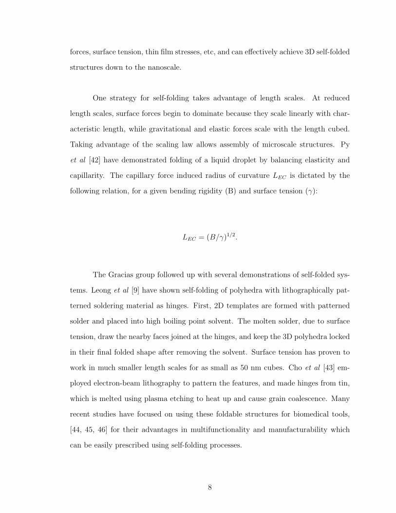
forces, surface tension, thin film stresses, etc, and can effectively achieve 3D self-folded
structures down to the nanoscale.
One strategy for self-folding takes advantage of length scales. At reduced
length scales, surface forces begin to dominate because they scale linearly with char-
acteristic length, while gravitational and elastic forces scale with the length cubed.
Taking advantage of the scaling law allows assembly of microscale structures. Py
et al [42] have demonstrated folding of a liquid droplet by balancing elasticity and
capillarity. The capillary force induced radius of curvature LEC is dictated by the
following relation, for a given bending rigidity (B) and surface tension (γ):
LEC = (B/γ)1/2.
The Gracias group followed up with several demonstrations of self-folded sys-
tems. Leong et al [9] have shown self-folding of polyhedra with lithographically pat-
terned soldering material as hinges. First, 2D templates are formed with patterned
solder and placed into high boiling point solvent. The molten solder, due to surface
tension, draw the nearby faces joined at the hinges, and keep the 3D polyhedra locked
in their final folded shape after removing the solvent. Surface tension has proven to
work in much smaller length scales for as small as 50 nm cubes. Cho et al [43] em-
ployed electron-beam lithography to pattern the features, and made hinges from tin,
which is melted using plasma etching to heat up and cause grain coalescence. Many
recent studies have focused on using these foldable structures for biomedical tools,
[44, 45, 46] for their advantages in multifunctionality and manufacturability which
can be easily prescribed using self-folding processes.
8

Folding by thin film stresses has been widely studied, because of its applica-
bility in sub-millimeter scales down to the nanoscale. The key to achieve self-folding
utilizing thin film stresses is based on the control of mechanical equilibria. For exam-
ple, in the case of a bilayer system with the top layer deposited under compression, the
system will relax in such a way as to generate opposite internal stresses constrained
to each other, and thus creating a bending moment. Stoney [47] and Timoshenko [48]
studied stress induced bending in thin metal films to describe the phenomena. The
film relaxation is governed by the following relation characterized by the deflection
angle θ, which is the length L over the radius of curvature (ρ):
θ =L
ρ= L
6ε(1 +m)2
(tf + ts)[3(1 +m)2 + (1 +mn)(m2 + 1mn
)]
Here, E is the elastic constant, ε is the strain, t the thickness, subscripts f and
s indicate film and substrate, respectively, m is tstf, and n is Es
Ef.
From the relation above, one can see that the curvature, and thus the deflection
angle, is a function of film thicknesses (tf and ts) and the control of strain (ε), which
are primarily determined by the deposition process. This relation can also be applied
to systems with strains arising from a variety of sources. Thus as thin film processes
and deposition techniques play increasingly important roles in multilayer devices,
studies in residual stresses during deposition have been critical to avoid delamination
and cracking. Later extended to other boundary conditions, carefully constructed
bilayers can be used for self-folding applications. Mismatch in lattice spacing, [32]
thermal expansion coefficient, [49, 50] and swelling ratios [51, 52] have been used to
create stresses in thin films to achieve different degrees of folding, reconfigurability,
and in different material systems. Other forms of thin film stress relaxation that
9

create pattern formation from bending, [53] rolling, [54, 55] and buckling [56] have
also opened up possibilities in making periodic or arbitrary micro- and nanostructures.
Shape memory alloys is also a convenient choice to engineer reversibility on
millimeter to centimeter scales. [57, 58] The folded and the unfolded states can be
achieved by repeatedly annealing and reshaping. Embedding these shape-memory
actuators with circuitry to heat up sequentially into a sheet allows one to “program”
the final folded shapes. Beyond alloys, Felton et al [59] have similarly used resistive
joule heating to achieve localized folding with polymer composites that contract above
their glass transition temperature.
These folded structures find many applications in biomedicine. Miniaturiza-
tion of biomedical devices, such as neural probes, [60, 61] is a prime example where
going into the third dimension can achieve wide-reaching impact. Besides accuracy,
reproducibility, and biocompatibility, biomedical devices must be made small enough
to minimize interference with the human body and in batches for medical use. To
fabricate high aspect ratio and functional probes, researchers have turned to folded
probes. Takeuchi et al [62] and Yao et al [63] created 3D arrays of microelectrodes
from 2D patterning techniques to increase the number of recording sites over a smaller
area at around millimeter scales using a magnet and custom jig, respectively.
10

Figure 1.4: Research effort in engineering origami focuses on using 2D patterningtechnique to generate 3D structures on small length scales. (A) An ex-ample of a 3-dimensional circuit; [7] (B) 3D neural probe [62] (C) Foldingcube using thin film stresses. [32]
Thus, origami provides a way to access three-dimensional forms from two-
dimensional starting materials, where the mechanics can be predictable due to the
geometry dependence. In the context of materials science, origami provides a way
to design deformation occurring on different length scales. This is fundamental to
materials science, where the manipulation of matter on a range of length scales dictate
the desired functional properties. By applying engineering origami, we can address
the need to engineer responsiveness into materials and dictate functionality.
1.1.3 Self-Assembled Molecular Origami
For many, the first image for the word “origami” in the engineering context
is DNA origami. In fact, a great deal of engineering origami in the literature deals
with folding of molecular chains. Manipulation of biological matters such as DNA
11

Figure 1.5: DNA origami as a bottom-up nanofabrication technique. (A) Arbitraryshapes formed by DNA self assembly [65] (B, C) Long strand of DNA(blue) folded into concentric circles using short staple strands. [69]
has also gained research attention in the past two decades to create arbitrary shapes
in the nanoscale using a bottom-up self-assembling technique, DNA origami. In the
molecular world, DNA is an intriguing building block for generating 3 dimensional
nanoassemblies.
The double helical structure of DNA and the combinatorially large set of base
pairs can be harnessed to design molecular interactions (Fig. 1.5). In 1980s, See-
man conceived the concept of DNA nanotechnology, inspired by the Escher woodcut
artwork to create 3D lattice out of linear strands of DNA. [64] By pre-programming
the resulting structure, DNA scaffolds are folded into 3D shapes by short staple
oligonucleotides. In 2006, Rothemund [65] created arbitrary shapes such as stars,
triangles, and lattice patterns with can be created with relatively good yield, using
staple strands to hold the long DNA chain in place. The success of this study has thus
further spurred the development of DNA origami to create nanocontainers and as a
template to arrange nanowires, nanotubes, and nanoparticles in space. [66] Later, it
has been shown that gold clusters can be coated with positively charged functional
groups and bind to negatively charged DNA. [67, 68] These strategies can be used to
manipulate nanomaterials and form arrays and hierarchical assemblies.
12

Variations of the DNA origami technique have also been proposed to create
complex and curved 3D structures. For example, Shih and coworkers [70] have re-
ported using insertion and deletion of base pairs to create twists and curves in DNA
origami nanostructures. By controlling the crossovers between neighboring helices,
it is also possible to design out-of-plane curvature in DNA origami, [71, 69] further
enabling the range of structures that can be made.
1.1.4 Novel 2D Materials
Outside of the context of molecular manipulation, origami by definition implies
that the starting materials are typically sheets. Besides deployability and new strate-
gies to manipulate thin sheets, engineering origami and kirigami have also sparked
interest in thin, 2D starting materials. Recent attention in novel 2 dimensional ma-
terials such as graphene has also been translated to the study of foldable systems.
Back in 1995, Ebbesen and Hiura [13] observed using the atomic force mi-
croscope that thin strips of graphite naturally fold in certain angles because of the
molecular structure. In particular, the rigid graphite sheet with sp2 hybridization can
form sp3 character when bending out-of-plane. It had been since proposed manipu-
lating graphitic sheets into desirable shapes using photolithography. With the rise of
graphene, the single atomic layer thick allotrope of carbon has been proposed to form
3D structures, much like fullerene and carbon nanotubes, which are considered folded
and rolled graphene sheets. Recently Blees et al [72] have reported kirigami pattern-
ing of graphene. It is expected that a single atomic layer of material should have a low
Foppl-von-Karman number, γ, which measures the ratio between in-plane stiffness
and bending stiffness. It is shown that the ripples that form in the graphene sheets
13

due to thermal fluctuation effectively increases γ by 3 orders of magnitude, close to
that of a sheet of paper. The implication is that instead of wrinkling, graphene can
be structured, patterned, and manipulated just like in paper art.
These one atomic thin materials such as graphene and molybdenum disulfide
become natural candidates to be shaped for applications in engineering origami and
kirigami. Using molecular dynamics, Zhu and Li [73] show that hydrogenation of
graphene can be used to fold nanocages. Similar to the observation in the graphitic
origami, hydrogenation of a carbon atom in graphene induces a structural change
from the sp3 carbon-hydrogen bond. Selective hydrogenation thus creates robust 3
dimensional shapes out of single graphene sheets. This folding scheme is suggested
for molecular mass storage and release. As an alternative to graphene, molybdenum
disulfide can also be used to for patterning to enhance the ductility and fracture
strains. [74] Molecular dynamics calculations show that the more complicated tri-
layer structure of MoS2 is similarly suitable for kirigami patterning.
Despite graphene’s remarkable thermal, electrical, optical, and mechanical
properties, there remain several challenges in translating the theoretical properties
into practical use. Large area graphene sheets are typically grown on metals us-
ing chemical vapor deposition and transferred later to the desired substrate. It is
well known that the quality is highly inconsistent under nominally identical condi-
tions. Defects such as grain boundaries strongly influence the functional properties
of graphene. [75] At the one-atom-thick regime, graphene is strongly influenced by
van der Waals forces, and therefore graphene is extremely sticky. [72, 76] The strong
adhesion property thus requires the graphene to be suspended or manipulated in so-
lution, and often a workable sample is left to chance. For the many proposed practical
applications, reliable methods that yield consistent properties in graphene is much
14
needed.
On the other hand, graphene-based nanocomposite materials many offer dis-
tinct advantages over graphene, considering its relative ease of preparation and tun-
able properties. Graphene oxide and platelets functionalized by epoxy, hydroxyl, and
carbonyl groups allow for stable dispersion in water, making them suitable for pro-
cessable nanocomposites. [77, 78] Combined with polymer, graphene-based nanocom-
posite can retain the electrical property above the percolation threshold. The control
over thickness and ease of handling also give advantages on using these nanocompos-
ites in practice as the bending stiffness scales with thickness cubed. The load-transfer
in polymer and graphene-based nanocomposites can also obviate the brittle fracture
observed in monolayer graphene. [79, 80]
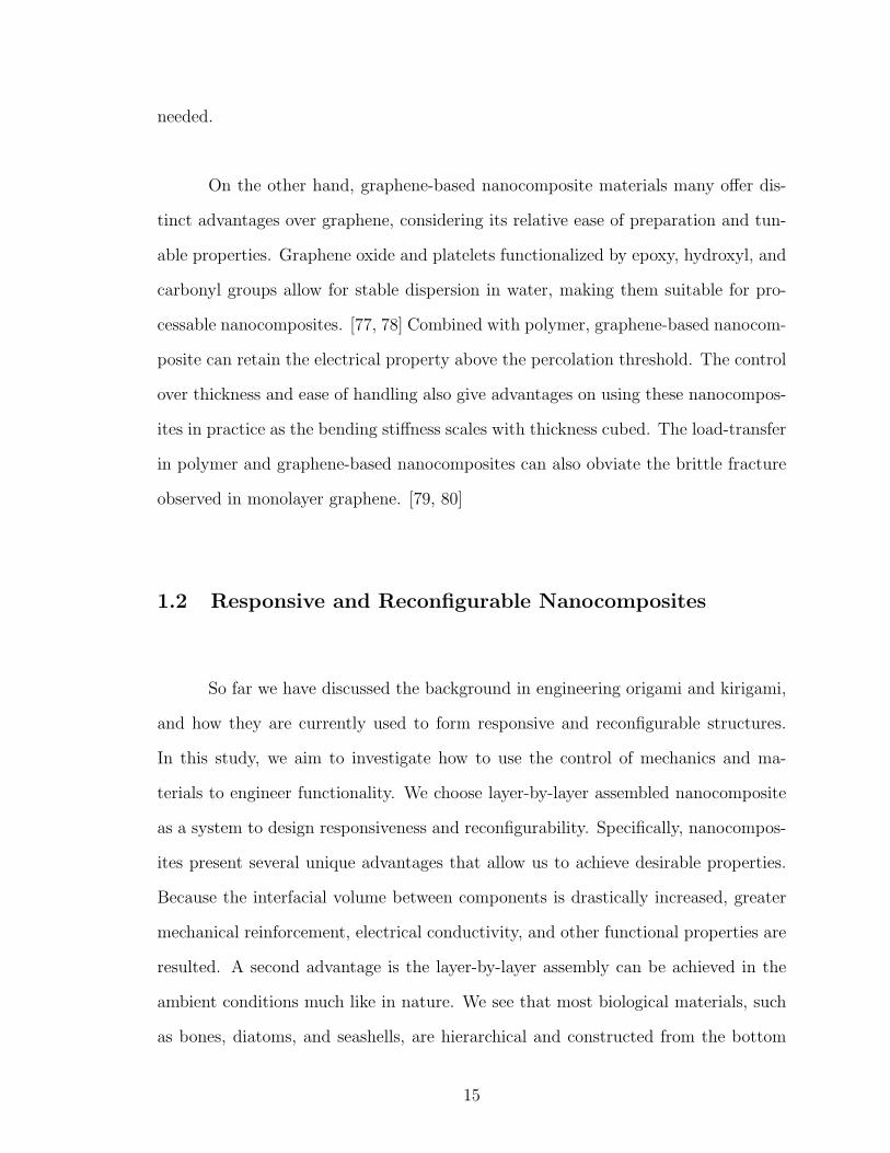
1.2 Responsive and Reconfigurable Nanocomposites
So far we have discussed the background in engineering origami and kirigami,
and how they are currently used to form responsive and reconfigurable structures.
In this study, we aim to investigate how to use the control of mechanics and ma-
terials to engineer functionality. We choose layer-by-layer assembled nanocomposite
as a system to design responsiveness and reconfigurability. Specifically, nanocompos-
ites present several unique advantages that allow us to achieve desirable properties.
Because the interfacial volume between components is drastically increased, greater
mechanical reinforcement, electrical conductivity, and other functional properties are
resulted. A second advantage is the layer-by-layer assembly can be achieved in the
ambient conditions much like in nature. We see that most biological materials, such
as bones, diatoms, and seashells, are hierarchical and constructed from the bottom
15

up, exhibiting a mix of the hybrid and architectured characteristics. [81, 82] As a
natural nanocomposite, bones comprise inorganic minerals and organic collagen and
demonstrate nanoscale to macroscale hierarchical structure. Their flaw-tolerance and
the range of properties achievable with relatively small number of building blocks are
often attributed to the sophisticated structural hierarchy. Drawing inspiration from
structural hierarchy from the bottom up, it is now possible to design hybrid materials
with nanoscale control. Further, the incorporation of zero-dimensional nanoparticles,
one-dimensional nanotubes or rods, and two-dimensional nanosheets provide tremen-
dous opportunity for modern materials scientists. The aim of this study is to use these
composites for tunable and multifunctional applications by incorporating design of
mechanics via origami and kirigami.
1.3 Focus of the Thesis
As we have seen in the previous section, responsive systems are widely studied
for metal and polymer systems, and manipulation of folded structures have also been
extended to the molecular scale and one-atom-thin materials. Using existing top-
down and bottom-up manufacturing methods, we experimentally demonstrate using
nanocomposites to engineer tunable, responsive, and multifunctional materials. We
also discuss the design of materials and on prescribing functionality. With engineering
origami and kirigami, the mechanical behavior of materials is directly tied with the
deformation mechanics. Applying these principles, we can control the components
and the spatial arrangement of the material, and design responsive materials based
on the control of deformation.
16

1.4 Organization of the Thesis
This thesis is organized as follows:
Introduction and Background. In this chapter, we have discussed the back-
ground of engineering origami, how these are relevant in applications across a range
of length scales, in optics, MEMS, biomedical engineering, and self-assembly, and the
scope of the thesis.
Methods and Techniques. In this chapter, the methods and techniques used
in this work are described, including characterization, mechanical analysis, and a
discussion on top-down and bottom-up fabrication and patterning techniques.
Responsive Inkjet Printed Layer-by-Layer Assembled Films. In this chapter, we
describe a system of layer-by-layer assembled film, which is used to engineer respon-
siveness. Because of a pseudonegative thermal expansion coefficient that is dependent
on the humidity of the surrounding, responsiveness can be used to create motion and
used as a visual indicator.
Engineering Properties with Kirigami Nanocomposite. Based on the under-
standing of strain-dependent conductivity in stretchable conducting nanocomposites,
we use a kirigami approach to control materials deformation. With this approach,
we can engineer strain-independent conductance over a range of strain, and suggest
possible applications.
Tunable Kirigami. Here we experimentally explore using strain-tunable kirigami
for modulating plasma properties other potential applications with tunable kirigami.
17

Summary and Future Directions. In this chapter, we summarize the findings
in this thesis, and how they inform future designs of responsive and tunable materials
systems. We discuss considerations in time scale, length scale, and the design of
deformation.
18
CHAPTER II
Methods and Techniques
2.1 Introduction
In this chapter, we describe the characterization techniques, and experimental
methods relevant to this thesis, including imaging techniques, mechanical analysis,
and fabrication techniques. The descriptions of the techniques provided here are not
intended to be exhaustive, but should instead serve as a guide for the chapters to
follow.
2.2 Microscopy and Imaging
Various microscopy tools are central to the materials characterization in this
work, which allows us to gain understanding of a material’s structure on a range of
length scales. In particular, scanning electron microscopy (SEM) is a commonly used
technique for imaging micro- and nanoscale features, with a resolution of down to 1
nm. Analogous to the idea of an optical microscope, a source of illumination in the
19

form of a high-energy electron beam is focused with a series of lenses onto the sample.
The equivalent of a lens for electron beams uses an electric field to deflect magnetic
field to focus. Electrons, like a light beam, can be reflected, or backscattered, from the
sample. Or, the electron can inelastically interact with electrons in the sample. The
ejected electrons are called secondary electrons. Backscatter electrons and secondary
electrons are the two primary modes of imaging. The electron beam is scanned line-
by-line across the sample under electrostatic and magnetic fields. From the interaction
between the electron beam and the sample, the emission of electrons or photons is
collected with a detector, allowing us to see the specimen. [83]
Conventional optical microscopy acquires sharp images only at the focal plane.
At high magnifications, samples with high level of corrugation, topological features,
or non-flat surface result in images that are primarily out-of-focus. Similar to conven-
tional optical microscopy, SEM also does not give 3D details or quantitative analysis.
To capture 3D information on a surface, laser confocal microscopy is currently widely
used as an optical and non-destructive technique. In 1961, Minsky invented the first
confocal microscope, [84] but at the time a sufficient light source did not exist for it to
gain much traction. Significant progress in optoelectronics and computer science later
on in 1970’s through 1990’s enabled commercial development of the instrumentation
and technology, where it is now widely used in biological specimens.
In laser confocal microscopy, a coherent laser beam is reflected by a dichromatic
mirror and scanned over the sample, and the reflected or scattered beam is delivered
through a pinhole aperture and into a photomultiplier. [85, 86] The light signal is
then reconstructed into an image on a computer. The out-of-focus signals are filtered
through a pinhole, and changing the focal plane location results in sequential slices of
images that allow for 3D reconstruction of an image that is in focus everywhere. The
20

advantages of the laser confocal microscopy include minimal to no sample preparation,
its non-contact and non-destructive nature, and the possibility to generate 3D slices
and quantitative data of sample surface. Furthermore, current technology can use a
white light source for true-color imaging, and an LED as a secondary light source to
enhance resolution.
2.3 Mechanics
2.3.1 Stress-Strain Behavior
The mechanical property of a material is determined by its stress-strain behav-
ior; one can measure the deformation of the material (strain) by applying a force over
an area (stress). For most stiff materials undergoing relatively low tensile stress, the
stress-strain relationship is linear through Hooke’s law, first stated in 1660, describing
the linear relation between force and extension. Thus, stress (σ) is related to strain
(ϵ):
σ = Eϵ
This proportionality constant E is the Young’s modulus, which is essentially a mate-
rial’s ability to resist elastic deformation.
Whereas the Hookean behavior describing linear elasticity is easy to charac-
terize and understand, the nonlinear elasticity common in biological, polymeric, and
hierarchical materials requires further understanding in the molecular and hierar-
21

chical structures contributing to the nonlinear response and complex deformation
modes. [87, 88, 89] Since the 1940’s, studies began to point the elasticity of rubber
toward the configurational entropy of stretched polymer chains. The elastic response
is dominated by the configurational entropy of the system, where a single elastic chain
has many curled-up configurations and only one straight configuration. [90] Hence,
stretching a single chain reduces its configurational entropy, and the restoring force
comes from increasing this configurational entropy. The strain-hardening, then, is
attributed to the fact that the molecular strands cannot be deformed indefinitely.
The deformation of elastic proteins have been widely studied for their wide
range of material properties relevant for their functional roles. [91, 92] Many elastic
biological materials exhibit a combination of the rubber-like entropic elasticity and
strain-hardening effect, where proteins are allowed to unfold during stretching. The
energy dissipation that between stretching and re-stretching cycles contributes to the
ability for many species to survive in mechanically harsh conditions.
In contrast to biological and polymeric materials, nonlinear elasticity observed
in man-made hierarchical materials is due to the different deformation modes or ge-
ometric effects. Cellular solids are a particularly interesting class of engineering ma-
terial that offer desirable strength-to-weight ratio, [93, 94, 95] where the deformation
is controlled by linear elasticity, buckling, and collapse. Because of the nonlinearity,
the elastic constant of the cellular material here is therefore not well-defined, even
though that of the bulk material is well-defined. The condition for buckling is such
that the load exceeds the critical buckling load (Pcritical),
Pcritical =n2π2EI
h2
22

where n is the rotational stiffness of the node where cell walls meet, which is
governed by the loading condition, I is the second moment of inertia (I = bt3
12for a
wall of uniform thickness t and width b), and h the wall height. [96]
Given the variety of different stress-strain behavior and the information from
which one can derive, it is useful to characterize the deformation response by measur-
ing the stress-strain behavior. This is often done with uniaxial tensile or compressive
testing, which yields various material properties by applying a uniaxial force on a
specimen until failure. Mechanical properties such as maximum elongation, yield
strength, Young’s modulus, and more can be obtained.
The tensile test is performed under quasi-static conditions, meaning that the
acceleration effect is insignificant on the load measuring devices, and the stress wave
propagation is insignificant within the sample. The quasi-static conditions thus differ
from sample to sample. Usually a slow enough rate at 0.01 s−1 is considered quasi-
static; however, to obtain strain rate invariant responses, one can decrease the strain
rates by an order of magnitude until further decreases does not change the stress-
strain behavior. [97]
2.3.2 Finite Element Modeling
Computer simulation techniques have established their increased practical im-
portance in many complex engineering and physical science problems. It is now pos-
sible to simulate interactions of matter from the most fundamental molecular motions
and intermolecular interactions, on the scale of molecular dynamics, to interactions
much greater than interatomic distances, such as continuum mechanics.
23

For purpose of our study, we focus on the continuum case. The continuum
hypothesis assumes that the characteristic length scale of interest falls within the
range where the local density per unit volume is insensitive at the length scale of
interest for arbitrary volume V . Here, the continuum description of the system is a
coarse-grained, smoothed distribution of continuous densities for mass, momentum,
and energy, for systems comprised of a large number of particles, N . [98] This is a
good description of the collective behavior of the system, but we should recognize
that the assumption breaks down when N is small compared to the length scale of
interest.
For mechanical structures with complex deformation and loading scheme, it
is useful to analyze deformation using continuum computational techniques, lending
us insights to stress concentration, and predict a large number of geometries and pa-
rameters. For example, the post-buckling behavior of cellular solids is often analyzed
by finite element modeling. [99, 100, 101]
Mechanical structures, regardless of their size and shape, can be broken down
into several structural forms, which are composed of smaller units of structural el-
ements. Solving differential equations in a continuum requires discretization and
approximation that, in the limit of appropriate discrete elements approach the true
continuum solution. Geometry, surfaces, tensile or compressive forces, and three-
dimensional materials properties all contribute to the analysis, which is often com-
plicated to solve by hand. This process is automated by numerical methods that
approximate the solution. In finite element modeling (FEM), the structure is dis-
cretized, or meshed, by dividing the structure into elements and nodes. A set of
linear equations are formulated with unknowns at each node, and the linear equa-
tions are solved to output stresses, strains, and displacements. Because the inputs
24

and boundary conditions are the same, the results of a given simulation is the same
for an FEM sample every time. The mesh size is decreased until the results do not
change with decreasing mesh size.
A number of commercial software packages are available for solving partial
differential equations in finite element models. In our study, we used Abaqus-C3D15,
a three-dimensional continuum elements code.
2.4 Fabrication Techniques
2.4.1 Thin Films
Thin films are relevant in everyday life in various applications, including optical
coatings, semiconductor devices, surface finishes, etc. There are many deposition
techniques to form thin films, including various types of physical vapor deposition
(PVD) and chemical vapor deposition (CVD) that produce thin metal, polymer, and
dielectric layers. These vacuum processes have highly controlled particle density and
stoichiometry, with the advantage of high uniformity, smooth coverage, and purity.
In contrast with these vacuum processes are ambient deposition techniques that also
enable fine control over nanoscale architecture, but have vastly different assembly
scheme. Here we focus on the discussion of layer-by-layer assembly (LbL).
LbL has been employed to fabricate a wide variety of nanocomposites that
combine seemingly incongruous properties, incorporating aspects of mechanical, elec-
trical, biological, thermal, and optical properties of the constituents. [60, 102, 103,
25

104, 105, 106, 107] Polyelectrolyte monolayers alternately adsorb, attracted to each
other by a number of intermolecular interactions, including: electrostatic, hydropho-
bic, hydrogen bonding, biological recognition, among others. The adsorption process
is repeated with nanometer control over layer structure, thickness, and composition.
LbL offers simplicity and versatility compared to other techniques with nanometer
control. LbL thin films are also considerably more stable in physiological conditions
due to the cooperative effects of multiple interactions among the film components.
In a typical LBL assembly process, glass or silicon substrates are cleaned with
piranha solution (3:1 sulfuric acid and 30% hydrogen peroxide). The clean slides are
dipped alternatively in oppositely charged polyelectrolyte solutions. These solutions
can take the form of polyanion, polycation polymer solutions, or various particle dis-
persions, allowing for ambient condition assembly and controlled architecture (Figure
2.1). To construct large numbers of bilayers with prescribed dipping time (5 min)
followed by rinsing and drying, a NanoStrata robot [108] is used. Other methods to
speed up and automate the LBL construction include spin-assisted and spray-assisted
LBL. [109, 110]
Vacuum-assisted flocculation (VAF) is an alternative construction method
[111, 78, 103] to assemble nanoscale components into nanocomposites, where mea-
sured amounts of polymer solution are combined with dispersed nanomaterial, and
filtered through with a vacuum filter. Similar to LbL, VAF also produces a layered
structure. Different from LbL, however, VAF is a much faster process while sacrificing
the level of precise nanoscale control. For example, stretchable nanocomposites have
been shown to have superior conductivity when made by LbL compared to VAF. [111]
26

Figure 2.1: Typical LBL assembly process. (A) Clean slides are dipped alternativelyin oppositely charged polyelectrolyte solutions, with rinsing and dryingsteps in between. (B) The clean substrates are positively charged. Mono-layer adsorption takes place during each dipping step, here polyanion,polycation, and nanoparticles are incorporated in a layer-by-layer fash-ion. Adopted from [107]
27
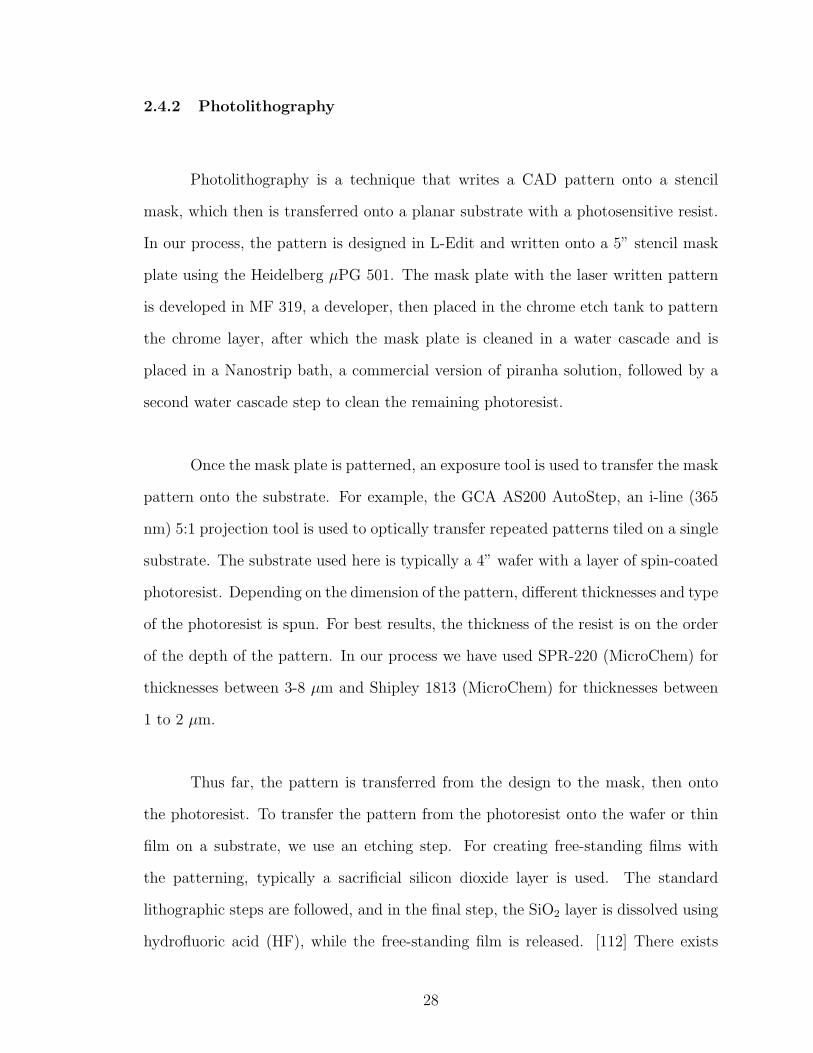
2.4.2 Photolithography
Photolithography is a technique that writes a CAD pattern onto a stencil
mask, which then is transferred onto a planar substrate with a photosensitive resist.
In our process, the pattern is designed in L-Edit and written onto a 5” stencil mask
plate using the Heidelberg µPG 501. The mask plate with the laser written pattern
is developed in MF 319, a developer, then placed in the chrome etch tank to pattern
the chrome layer, after which the mask plate is cleaned in a water cascade and is
placed in a Nanostrip bath, a commercial version of piranha solution, followed by a
second water cascade step to clean the remaining photoresist.
Once the mask plate is patterned, an exposure tool is used to transfer the mask
pattern onto the substrate. For example, the GCA AS200 AutoStep, an i-line (365
nm) 5:1 projection tool is used to optically transfer repeated patterns tiled on a single
substrate. The substrate used here is typically a 4” wafer with a layer of spin-coated
photoresist. Depending on the dimension of the pattern, different thicknesses and type
of the photoresist is spun. For best results, the thickness of the resist is on the order
of the depth of the pattern. In our process we have used SPR-220 (MicroChem) for
thicknesses between 3-8 µm and Shipley 1813 (MicroChem) for thicknesses between
1 to 2 µm.
Thus far, the pattern is transferred from the design to the mask, then onto
the photoresist. To transfer the pattern from the photoresist onto the wafer or thin
film on a substrate, we use an etching step. For creating free-standing films with
the patterning, typically a sacrificial silicon dioxide layer is used. The standard
lithographic steps are followed, and in the final step, the SiO2 layer is dissolved using
hydrofluoric acid (HF), while the free-standing film is released. [112] There exists
28

Figure 2.2: Typical lithographic steps. (A) A film is deposited on silicon dioxide glassslide or sacrificial layer. (B) Photoresist is spin-coated. (C) Using a stencilmask, the pattern is transferred onto the photoresist. (D) Photoresist isdeveloped. The film is patterned using plasma etching, and cleaned withacetone. (E) Dilute hydrofluoric acid is used to detach the patterned filmto create (F) a free-standing film.
many ways to fabricate SiO2 layers, each with different deposition characteristics and
etch rates. Generally, thermally grown oxides are formed by oxidizing bulk silicon,
and chemical vapor deposited oxides are formed by chemical reactions between silicon
and vapor and gaseous species. Because HF etches only SiO2 and not react with bulk
silicon, etching sacrificial SiO2 is commonly used to create mechanical parts in MEMS.
And in our process, this gives us an easy route to release patterned thin films.
Dilute or buffered hydrofluoric acid is typically used for removal of silicon
dioxide. Alternatively, photolithography process can also be performed on glass slides,
and HF can be used to lift off thin films deposited on glass slides. The schematics of
the process is shown in Figure 2.2.
29

2.4.3 Etching
Wet etching is a technique where an etchant in the liquid phase is used to
remove material from the wafer. To etch bulk silicon, proper masking is crucial to
ensure selective removal of the material in corrosive environments. Wet etching is
a chemical process, and in most materials this is isotropic; the exception is single
crystal materials where the different crystal orientations have different etch rates due
to the difference in surface energy. Chemical etching consists of three steps: first, the
reactive species are adsorbed onto the surface, followed by the chemical reaction, and
finally the desorption of reaction products. Each step contributes to the etch rate, in
addition to temperature and concentration, which affect the overall kinetics.
In a typical process of silicon wet etching, silicon nitride is used as a mask, and
80◦C 35% potassium hydroxide (KOH) as an etchant, with an etch rate of around 1
micron per min in the <100> direction. Isopropanol is added to minimize roughness.
In wet etching, the selectivity of {100} and {111} planes are about 400:1. Thus wet
etching is commonly used for creating anisotropic features, where the {111} plane
acts as a natural etch stop. The selectivity have been widely used to create polygonal
silicon templates.[113, 114]
In contrast with wet etching, dry etching [115] involves a gas phase etchant
in a plasma, containing reactive ions, free electrons, and free radicals. Typically a
chamber is evacuated to low pressure, reactive gases introduced, and an electric field
is supplied to create and mobilize ion species in a plasma. Etching occurs when
the ionized species react with material surface, forming a volatile compound that
is carried away by the gas flow. This process removes the material of choice at a
rate controlled by the pressure, flow rate, and RF power, and dimensional resolution
30

controlled by the flux and the masking resist.
2.4.4 Inkjet Printing and Additive Manufacturing
Inkjet printing technology is a versatile deposition technique for the printing
industry, and more recently in thin-film electronics and medical applications. Several
reviews [116, 117, 118] describe in detail the historical background and future outlook
for inkjet printing technologies. Inkjet printing is attractive for a variety of reasons
in manufacturing, because it does not require templates and masks to create intricate
shapes and can minimize materials waste. The first inkjet printing device was invented
by Lord Kelvin in 1858 for recording of telegraph messages using electrostatic forces.
The mechanism of droplet formation from a stream jet was then described by Lord
Rayleigh. [119] Several studies related to the fluid dynamics of jet breakup followed,
relating theoretical understanding in surface tension, electromagnetic forces, and the
piezoelectric effect. It was not until 1951 (US Patent 2566,433) that the first inkjet
printer was patented using the Rayleigh description of inkjet breakup. Since then,
many types of inkjet printing technologies were developed to manipulate droplet
deposition. These techniques can either be continuous or drop-on-demand (DOD).
The continuous mode is operated by applying a pressure wave pattern to break
up a continuous stream, typically used for high speed printing. DOD inkjet print-
ing [118] is used widely for its precise drop size and spatial control, in addition to
other advantages afforded by the inkjet printing technique, including high level of
customization and waste minimization. The ink droplets are formed by a voltage ap-
plied to a piezoelectric crystal, which generates a pressure pulse that propels picoliter
droplets in a reservoir from the nozzle, allowing for precise patterning.
31

In this work, we use a commercial inkjet printing system (FUJIFILM Dimatix
Materials Printer DMP-2831), and piezo-based 16-nozzle jet cartridge, which can be
filled with the desirable ink formulation. Some of the important characteristics for
the ink formulation include the viscosity, surface tension, evaporation rate, and pH.
[120] The viscosity should be maintained between 10-12 cPs, and the printhead can
be heated to lower the viscosity of the printing fluid. The surface tension should
be between 28-33 dynes/cm, and surfactants and additives can be used to achieve
the desirable surface tension range. The evaporation rate is controlled such that the
ink does not dry at the nozzle. Solvents can be added to control the evaporation
rate. Lastly, the pH is maintained between 4-9 to ensure no corrosion occurs at the
printhead.
Besides the rheological properties, the inks should be filtered using a 0.2 µm
filter to ensure fluid flow through the nozzle. The rule of thumb is that any particles
in the fluid must be 100 times smaller than the diameter of the nozzle. For the com-
mercial 10 picoliter nozzle, this diameter is 21 µm. Hence, most non-agglomerating
and well-dispersed nanoparticles are compatible with the inkjet printing technique.
Based on the control of the ink composition, print parameters, and rheological
properties, the control of intricate printed structures can be realized, and incorpora-
tion of metallic and ceramic components is possible. Recent development in direct-ink
writing, [121, 122] for example, demonstrates the potential in emerging area of ad-
ditive manufacturing. These techniques are convenient tools to dictate the structure
and spatial arrangement of material, with tailored mechanical, thermal, and electrical
properties.
32

CHAPTER III
Responsive Inkjet Printed Layer-by-Layer
Assembled Films
In this chapter, we use inkjet printing as a patterning technique to create
stimuli-responsive LBL nanocomposites. In particular, LBL has important techno-
logical significance in creating nanostructures with controlled thickness, morphology,
and functionality, and is suitable for modifying surfaces in the context of contact an-
gles. Initially developed for oppositely charged polyelectrolytes, LBL has been shown
suitable for a diverse range of nanoscale building blocks, including proteins, nanopar-
ticles, colloids, and dendrimers. In conjunction with inkjet printing, LBL has also
been shown a versatile technique to create selectively patterned nanocomposites with
customizable architecture that can be used to modify surfaces. [123, 124]
In the first part of the chapter, we discuss a strategy to fabricate a layer-by-
layer assembled, solid stimuli-responsive nanocomposite based on relative humidity
changes in the environment. Origami, the Japanese art of paper folding, has inspired
a body of studies on self-folding and reconfigurable systems, where 2D patterns com-
patible with traditional 2D patterning techniques are transformed into functional 3D
33

objects. These self-reconfiguring systems can create structural materials that auto-
matically assume different configurations based on environmental cues. Successful
development and implementation of reconfigurable structures with fast throughput,
high customization, and precise spatial control will enable applications in dynamic
buildings, aerodynamic skin, microfluidics, sensing, and more. On a larger scale,
these self-reconfigurable systems may significantly improve efficiency and reduce en-
ergy consumption.
Next, we describe a novel approach to use this humidity responsiveness in
layer-by-layer assembled films by creating inkjet printed patterns on a substrate with
controlled wettability. The difference in wettability as measured by contact angle be-
tween the LBL modified, hygroscopic inkjet patterned area and the superhydrophobic,
nanopillar decorated areas gives rise the appearance of hidden images when the sur-
face is fogged by human breath. Potentially usable for anti-counterfeit labels and
decorative purposes. The humidity responsive materials point to a unique outlook on
how we can think about stimuli-responsive systems and their role in technology.
3.1 Inkjet Patterning of Nanocomposites
As previously discussed in the first chapter, foldable structures and stimuli re-
sponsiveness are particularly attractive for mechanical motion in sub-millimeter scales
and smaller, because manual manipulation of foldable parts becomes less practical
and precise folding emphasizes this challenge. Therefore, it is desirable to devise
a new paradigm of manufacturing in which the structures self-fold into their func-
tional forms. To create folded 3D structures, several methods have been developed.
These include top-down methods such as focused ion beam, molding, [125, 126] and
34

stereolithography, and bottom-up approaches such as additive manufacturing and
self-assembly. [127, 128, 129, 65] Whether it is to make large or small structures fold
on their own from an external stimulus, generating a bending moment is crucial to
fold out of the plane. Many strategies have been explored and roughly categorized
into a few types to create this bending moment: surface tension, [42, 9, 130] shape
memory materials, prestressed or swellable polymers, [131, 132, 53, 133, 134] and
thin film stresses. [135, 136, 137] However, significant challenges remain to create
curved and angled structures, and those that allow large range of motion. Another
challenge is that these self-folding structures often require swellable polymers, hy-
drogels, or molten metals, which inherently do not allow for reversibility. The idea
of using nanocomposites has not been widely explored. To generate completely re-
versible self-folding structures, a different approach must be used. We will discuss how
we can use LBL nanocomposites to generate out-of-plane motion using the inherent
pseudonegative thermal expansion property found in these LBL systems.
Here we focus on a particular material system of LBL assembled nanocom-
posites and inkjet patterning. LBL processes are typically water based, and thus
compatible with inkjet printing technology without extensive modification. [138, 124]
Combined with the LBL process, inkjet printing enables fast assembly of a variety of
nanocomposites including proteins, nanoparticles, colloids, and biomaterials. Inkjet
printing assisted LBL also presents to advantage of eliminating the intermediate, often
time-consuming, rinsing step. Important to note, however, is that this intermediate
step in a typical LBL assembly process is important to prevent the formation of ag-
gregates and essential in thermodynamic stability within the multilayers. [123, 139]
Thus, in inkjet-assisted LBL, precise amounts and concentrations of material must
be delivered, and the viscosity and droplet spreading on the substrate are important
parameters to control the resulting multilayers. For this study we specifically focus on
35

a system based on LBL assembled cationic poly(diallyldimethylammonium chloride)
(PDDA) and anionic poly(sodium 4-styrenesulfonate) (PSS) for its thermal response
(Fig. 3.1).
Andres et al [140] demonstrated the utility of inkjet printing technique to
directly pattern responsive hinges required for reconfigurable nanocomposite origami.
P3 single-walled carbon nanotube (CNT, 0.25 mg/mL dispersed in water) and cationic
polyurethane (PU, Hepce Chem Co., South Korea, Mw 92,000) were used for the LBL
assembled nanocomposite, and (PU/CNT)200 was constructed using a typical LBL
process.
On top of this (PU/CNT)200, cationic poly(diallyldimethylammonium chlo-
ride) (PDDA) and anionic poly(sodium 4-styrenesulfonate) (PSS, Mw 70 000) were
chosen for the as complementary pairs for the inkjet printed layer-by-layer assembly
(Fig. 3.2). The inkjet printed polyelectrolytes assemble into complexes and give rise
to electrostatically-held swellable multilayer structures that are strongly influenced
by the ambient relative humidity. [141, 142, 143] Reversible water absorption and
desorption result in reversible volume changes in the polyelectrolyte complexes. [144]
LBL films assembled in this manner produce much more mechanically robust struc-
tures compared to swellable hydrogel. In addition, these films are often porous in
nature, which allows for rapid water transport suitable for fast response time (t in
the seconds range for solid thin films).
The thermal properties as characterized by the coefficient of thermal expansion
were determined using a thermal mechanical analyzer (TMA, Perkin Elmer) over a
temperature range. Between 35 and 75◦C, the CTE of (PDDA/PSS)250 was deter-
mined to be -368 ± 9 ppm/◦C, compared to -6.5 ± 9 ppm/◦C for (PU/CNT)200.
36

Figure 3.1: The molecular structures of cationic poly(diallyldimethylammonium chlo-ride) (PDDA) and anionic poly(sodium 4-styrenesulfonate) (PSS).
Figure 3.2: Schematic of a an inkjet printing assisted LBL process. (a) Cationicdroplets are expelled from the inkjet nozzle, followed by (b) anionicdroplets. (c) Sequential alternating complementary cationic and anionicdroplets reverse the charges on the surface during each inkjet depositionlayer and finally forming an (d) LBL composite.
37

It was found that the dependence of temperature with the CTE was related to the
relative humidity, where the CTE becomes more negative, from -5.3 to -368 ppm/◦C
as the relative humidity is increased from 0.37% to an ambient humidity of 25%.
We call this humidity-dependent coefficient of thermal expansion (CTE) pseudoneg-
ative (PNTE), because of the dependence on water sorption. [145] The PNTE be-
havior in these LBL assembled films suggests their suitable application in humid-
ity/heat stimuli-responsive systems. As illustrated with the inkjet printed responsive
(PDDA/PSS) layers on thin (PU/CNT) strips, heating using an IR lamp is enough
to drive humidity out of the system with response time on the order of minutes. The
actuated response in deflection angle corresponds well with the earlier Timoshenko
equation, given in deflection angle θ:
θ =L
ρ= L
6(a2 − a1)(1 +m)2∆T
(tf + ts)[3(1 +m)2 + (1 +mn)(m2 + 1mn
)]
The predicted deflection angle matches well with the experimentally observed
values, suggesting that the PNTE contributes to the self-folding of a nanocomposite
patterned by inkjet printing.
3.2 Contact Angle and Wettability
Inkjet assisted LBL assembly can also be used as a tool to alter the wettability
of a surface. In this section, we describe how we can apply this technique to make a
breath-activated stimuli responsive surface.
38

Figure 3.3: Schematic of a droplet residing on a solid surface and energy balance,depicting the interface tensions and the contact angle θ.
Engineered surfaces with different degrees of wettability find important ap-
plications such as coatings, aero- and hydrodynamics, and self-cleaning fabrics. At
equilibrium, the forces per unit length acting on the line of contact is zero (Fig. 3.3).
The angle that the droplet makes at the solid, liquid, and air interfaces is the contact
angle, given by the Young’s relation:
γSL − γSG + γLGcosθ = 0
or commonly expressed as
γSG = γSL + γLGcosθ
Thus, wettability is commonly characterized by the contact angle (CA), rang-
ing from 0◦ - which indicates complete wetting, where liquid spreads on the surface
and the surface is known as superhydrophilic - to 180◦ - which indicates complete
non-wetting, where the liquid beads up, and the surface is superhydrophobic.
39

In practice, textured and hierarchical structures yield good superhydrophobic
surfaces. Whereas a fully wetted state called the Wenzel state causes a droplet to cling
to a surface, the Cassie-Baxter state yields a composite liquid-air interface on top of
the textured surface, in which a droplet tends to roll off easily. [146, 147] This effect
can be understood in terms of the apparent contact angle (θ∗), which depends on the
contact area between the solid-liquid interface, supported on a composite liquid-air
interface due to the surface texture. [148] We can define a dimensionless measure
as a design parameter, D∗. Here, D∗ = [(R + D)/R]2, where R is the radius of the
texture, and D is half the inter-feature spacing, assuming regular surface features. In
terms of D∗, the Cassie-Baxter relationship is represented as
cosθ∗ = −1 +1
D∗ [π
2√3(1 + cosθ)]2
This relationship tells us that at increasing D∗, the actual contact area be-
tween the liquid and the solid is decreased, and the apparent contact angle tends
toward 180◦, which is superhydrophobic. This also implies that to maintain the su-
perhydrophobic property, the surface texture needs to be maintained.
Indeed, because of the dependence of contact angle on surface texture, a critical
challenge in engineering surface properties lies in how one can maintain the hierar-
chical surface features. [149, 150] As we create more hierarchical surface features in
decreasing length scales, these small features can be easily damaged during mechan-
ical abrasion, which renders these superhydrophic surfaces impractical. We also note
that there are effects of dynamic hydrophobicity, where the contact angle hysteresis
and sliding angle are important measures for hydrophobicity in a dynamic case. [151]
For the purpose of this study, we will focus on the static case. In the following sec-
40

tions, we discuss the newly developed PUNO nanopillars as a mechanically robust
platform to create a range of hydrophobicity and on top of which to selectively pattern
regions of different wetting behavior.
3.2.1 Nanopillar arrays
3D nanoscale surface features can strongly influence adhesion, interfacial inter-
actions, fluid flow, heat transfer, and other phenomena in the macroscale. [152, 153,
154] Numerous examples of 3D nanoscale features that profoundly influence surface
properties are found in nature. The lotus effect famously exemplifies the combination
of these 3D nanoscale surface features and chemical properties on the leaf surface
that contributes to the superhydrophobic and self-cleaning properties. Another ex-
ample where the sum of all individual nanoscale features contributes to macroscopic
effect can be seen in geckos. Gecko’s foot hairs, ranging between 200-500 nm, are
at the length scale where capillary and van der Waals forces are about comparable.
It is thus postulated that while each individual hair contributes only about 10−7N ,
millions of these hairs give geckos their famed ability to support their own weight on
walls of different hydrophilicities. [155] To artificially create these high aspect ratio
features, typically one of several approaches is used, including hydrothermal seed-
mediated growth, [156, 157] templated growth, [158, 159] and for periodic patterns,
lithography. [160]
In order to increase throughput for large scale fabrication of nanopillars, we
have focused on a molding process that uses a master mold created with silicon
fabrication technology with deep reactive ion etching. Subsequent polymeric replicas
can be made to produce sheets of patterned pillar and hole arrays and compatible
41

Figure 3.4: Schematic steps to create the nanopillar mold. (1) Thermal oxidation ofsilicon wafer; (2) dry etching to create desired aspect ratio; (3) once themaster mold is obtained, the polymer blend is poured on top to create anegative; (4) alternating positive and negative replications can be createdusing this process. Bottom depicts the nanohole arrays and nanopillararrays created by the molding process. [152]
with large scale roll-to-roll processes.
As seen in Fig. 3.4, to create the master molds, silicon wafers are thermally
oxidized to have a layer of 500 nm of SiO2 surface. The surface is patterned by
photolithography using a KrF scanner and etched using a mixture of Cl2, HBr, and
O2 to form the initial master nanopillars. The dimensions and aspect ratios are
finetuned by the oxidation time and etching conditions. [152]
42

Figure 3.5: SEM images of the nanopillars after 1000 rubbing cycles, showing defor-mation of pillars but no damage.
To create these nanopillar arrays, the nanomolding process, in practice, re-
quires an optimal balance between the adhesive force and the mechanical strength
to create durable nanopillar structures. That is, the adhesive force needs to be high
enough to ensure high fidelity of the replicated shape, while soft enough to be de-
formed and removed from the template, and at the same time mechanically strong
enough to remain their shape once the template is removed. This optimal adhesion
versus mechanical strength is found in a special blend of polyurethane acrylate (PU)
and an adhesive NOA63, denoted as PUNO. This PUNO polymer blend, while under-
going UV curing, shrinks about 1.3%, which allows for detachment from the template
(Fig. 3.5). With additional chemical modification, the polymeric high aspect ratio
nanopillar surface creates a convenient platform that can support a spectrum of sur-
face wettabilities, ranging from superhydrophobic to superhydrophilic, which is also
dependent on the aspect ratio, as controlled by the silicon dioxide doping thickness
(Fig. 3.6.a). This level of control will enable responsive smart materials based on the
difference in wetting properties.
43
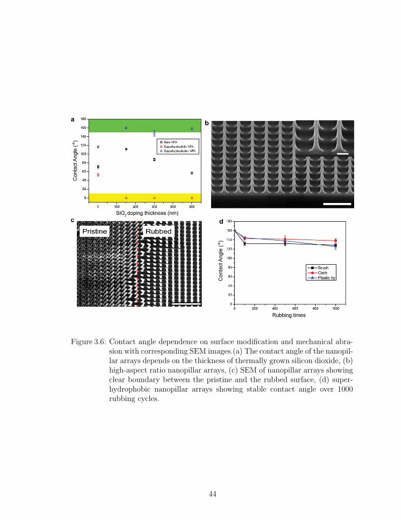
Figure 3.6: Contact angle dependence on surface modification and mechanical abra-sion with corresponding SEM images.(a) The contact angle of the nanopil-lar arrays depends on the thickness of thermally grown silicon dioxide, (b)high-aspect ratio nanopillar arrays, (c) SEM of nanopillar arrays showingclear boundary between the pristine and the rubbed surface, (d) super-hydrophobic nanopillar arrays showing stable contact angle over 1000rubbing cycles.
44

In nanostructured materials such as the nanopillars used here, the mechanical
integrity is crucial to maintain the surface properties during use. It can be seen that
nanopillar arrays maintain mechanical integrity after rubbing by bending deformation
rather than structural damage. Clear boundaries between rubbed and pristine surface
can be seen, but the nanopillars remain on the surface after 1000 rubbing times (Fig.
3.6).
3.2.2 Local Contact Angle Modification Using Inkjet LBL
Contact angle is a common way to determine how well a droplet wets a surface,
where low contact angle indicates good adhesion (hydrophilic), and high contact angle
indicates poor adhesion (hydrophobic), based on the Young’s equation. Site-selective
patterning of the contact angles has shown uses for ambient condensation harvest-
ing, microchannels and reactors, heat transfer, and templated thin film growth. [46]
Kobaku et al [161] have shown using mask or photoresist to pattern sub-millimeter
superomniphobic or superomniphilic domains on a highly porous electro-spun surface.
Because liquid condensation nucleation rate is strongly dependent on the hydrophilic-
ity, it is possible to tune the nucleation rates using the characteristic contact angle.
The condensation property on a given surface can thus be tuned based on the local
wetting property. We thus postulate that the ability to direct write a spectrum of
hydrophilicities will give us a handle to dynamically control the visual appearance of
a surface with patterned hydrophilicities as the relative humidity changes.
The inkjet deposition technique gives the leverage and versatility to create
complex shapes with nanometer control over the thickness on microscopic lateral
dimensions. Combined with LBL, because the droplets are precisely deposited as
45

opposed to dip-coated in the conventional LBL assembly, the rinsing step is eliminated
and allows for rapid assembly time. Ultimately, we would be able to manufacture high-
throughput, ordered nanopillared surface with microscale control over the surface
property. Using inkjet LBL, we can selectively alter local contact angle to pattern
hydrophilic regions on a hydrophobic surface.
Here, we used a process similar to previously described,[140] using cationic
poly(diallyl-dimethylammonium chloride) (PDDA) and anionic poly(sodium 4-styrene-
sulfonate) (PSS, Mw 70 000) as complementary pairs for the layer-by-layer assembly.
High molecular weight PDDA and PSS were diluted to 0.0025 wt% in deionized water
as the positive and negative polyelectrolytes, respectively, and filtered through 0.22
µm filters. The patterns were printed using Fujifilm-Dimatix inkjet printer and alter-
nating cartridges (10 pL drop volume) containing the solutions of PDDA and PSS.
Jetting conditions were optimized by adjusting the drive voltage-time waveform for
the piezoelectric print-head to produce stable drops. Four bilayers of ink were printed
and dried at 35◦C in between prints for 2 min on the printer plate, followed by drying
on a hotplate for 1 h after the printing steps.
46

Figure 3.7: Overt and covert images printed on nanopillar arrays using inkjet LBLdeposition. Photographs of the nanopillars with hidden images (a) beforeand (b,c) after exposed to breathing. (d) an overt image printed onnanopillar arrays. (e,f) SEM images showing differences between areasmodified by LBL and pristine nanopillars.
3.3 Overt and Covert Images
After inkjet modification of the surface, it is possible to create overt and covert
images by the dynamic control of the visual appearance of the nanopillar surface (Fig.
3.7). Depending on the number of layers deposited, either overt or cover images can
be created. At less than 3 deposited PDDA and PSS bilayers, the nanoscale coating
on the nanopillars does not alter the visual appearance of the film significantly. But
because of the changes in wettability between the patterned and non-patterned areas,
the few bilayers of the hygroscopic pattern is enough to tune the local contact angle,
such that when the printed invisible pattern is exposed to relative humidity change,
the images become visible.
With increasing number of bilayers, on the other hand, the spacing between
nanopillars becomes filled, creating contrast between the printed pattern and the
47

pristine nanopillar region. At 5 bilayer and above, the printed pattern becomes
visible to the naked eye without having to fog the surface.
Thus, we have demonstrated using transparent LBL coating to modify a nanos-
tructured, superhydrophobic surface, which can be used for anti-counterfeit labeling
and authentication. Future studies on the formation of patterns on nanopillar surfaces
will pave way toward manipulation of nanoscale surface effects.
3.4 Conclusion
In this chapter, we first surveyed the strategies to create stimuli-responsive
systems, focusing on shape-morphing systems inspired by the art of origami. The LBL
inkjet printing technique is employed to create hydrated polyelectrolyte multilayers
capable of shape transformation on top of a solid nanocomposite, in response to
temperature and humidity changes. The reversibility indicates negligible structural
changes within the nanocomposite during the shape transformation and robustness
of the inkjet printed LBL technique. Possible future direction includes incorporation
of plasmonic nanomaterials that have spectral selectivity to responsiveness. The
patternability and responsiveness pave way to a range of smart material design.
With the same humidity responsive hydrated polyelectrolyte multilayers, we
have also demonstrated a novel application for the stimuli-responsiveness. Based on
the idea of selectively modifying surface wetting property, inkjet patterned polyelec-
trolyte multilayers combined with nanostructural features such as nanopillar arrays
can be used to pattern hidden images that are revealed using human breath. Using
the inkjet patterning technique, we are able to dictate the spatial arrangement of
48

materials on a selectively. With control of the nanoscale components and features,
we can engineer materials that respond to environmental cues.
Future studies in these materials systems may involve investigating the adhe-
sion between the inkjet deposition and the substrate material. Further, the interac-
tion between the molecular chains of PDDA and PSS and the water can be further
fine-tuned for the level of responsiveness. It is also worth considering the structural
changes within the LBL multilayers during water sorption and desorption.
49

CHAPTER IV
Engineering Properties with Kirigami
Nanocomposite
By designing the deformation of materials, simple mechanical movements and
bistability can be used to couple the deformation mechanics to the functional prop-
erties of materials. [82, 153, 134] This coupling effect can give rise to possibility in
metamaterials on every length scale. [21, 22] In this chapter, we explore how we can
design the deformation of materials by using simple cutting patterns, borrowing the
concept from the art of paper cutting known in different cultures as jianzhi, kirigami,
monkiri, or silhouette. We use the term kirigami because of the greater emphasis of
this Japanese technique on repetitive patterns and their effects on three-dimensional
deformations of paper sheets. We highlight in this work, that the design of deforma-
tion based on the kirigami patterning technique can have wide-reaching impact. Here
we show the control of strain-conductivity relationship, eliminating the unpredictable
strain effects in nanocomposites by controlling the deformation. We will also explore
some potential applications related to the reconfigurability in the following chapter.
50

4.1 Background
Strain engineering has become increasingly important for the next generation
of nanocomposites, enabling the combination of mechanical and electrical proper-
ties typically unattainable in traditional metals, ceramic, and polymers. [111, 162]
There is a great need to further expand the range of accessible strain states and
develop new ways to deterministically control strain-property relationships in these
systems. [163, 164, 165] The development of multifunctional elastic nanocomposites
requires the control of deformation and failure mechanisms in order to retain func-
tional properties under high strains. It is known that stress failure of stiff and brittle
materials strongly depends on stochastically-distributed nanoscale and microscale de-
fects, which serve as stress concentrators that promote propagation of microcracks,
leading to failure. Many natural and man-made nanocomposites, combining hard
and soft components can arrest the propagation of microcracks but their ultimate
strains do not exceed 5% at high loading of the stiff components. [166, 167] On the
other hand, the stress concentration can be avoided in highly elastic nanocomposites
and one can reach strains as high as 470% but some of the functional properties, e.g.
conductivity, has to be sacrificed. [111, 162] Interfacial stiffening of polymers chains
at the interface with nanoscale components severely limits macroscale elasticity of
composites and their ability to relax local strain singularities. Accounting for strain-
induced restructuring in several interdependent components adds to the complexity
of the multiscale deformations in nanocomposites, and makes predictive modeling of
their tensile behavior an arduous task.
In this work we investigate a possibility to increase strain capabilities of highly
conductive but stiff materials, borrowing the concept from kirigami. The kirigami
technique has recently been used to engineer reversibly deformable two-dimensional
51

(2D) and three-dimensional (3D) structures, in which patterns of periodic cuts give
rise to emergent mechanical behavior. [72, 11, 21] We show that even simple kirigami
patterns can offer unprecedented control over stretchability, with only negligible im-
pact on conductance. From this framework, we demonstrate the possibility of mak-
ing a smart material from the combination of stretchability and conductivity using
kirigami nanocomposites.
4.2 The Kirigami Approach
In this work we show that in traditional kirigami, highly periodic cut patterns
are introduced into paper sheets to attain desirable topology upon folding. Using
standard top-down technique such as photolithography (Fig. 4.1 a), we can extend
the technique to micro- or potentially nano-scale. This fabrication process offers
scalability and accuracy, providing us the possibility to produce similar patterns across
multiple length scales. Here the homogeneity of material must be commensurate
with the length scale of the kirigami cuts, which is true for many nanocomposites
exemplified by grapheme oxide multilayers made by vacuum assisted filtration (VAF)
or layer-by-layer assembly (LBL) techniques (Fig. 4.1 b). [78] By measuring the
stress-strain response and comparing it to finite element calculations, we show that
mechanical deformation introduced by kirigami patterning may be used to engineer
elasticity and multi-functionality.
52

Figure 4.1: Microscale kirigami patterns. (a) Schematic of the kirigami microfabri-cation process. (1) A nanocomposite is deposited on a solid substrate forpatterning; (2) Photoresist is deposited and developed; (3) An oxygenplasma etch through the nanocomposites creates kirigami patterns; (4)Nanocomposite sheet is detached from the substrate. (b) Scanning elec-tron microscopy of the cross-section of a GO-PVA nanocomposites; (c, d)Two examples of microscale kirigami patterns in GO-PVA nanocompos-ites after photolithography. The insets show the corresponding kirigamiunit cells.
53

4.3 Mechanical Behavior
A simple kirigami pattern consisting of straight lines in a centered rectangu-
lar arrangement (Fig. 4.2 inset) made of tracing paper (Youngs modulus, E = 1.2
GPa) provides an experimentally convenient model for this study. It has allowed us
to develop a comprehensive description of deformation patterns taking place in such
material. The original material without patterning shows a strain of 4% before fail-
ure; its deformation primarily involves stretching of the individual nano- micro-, and
macroscale cellulose fibers (Fig.4.2 gray curve). With a single cut in the middle of
the sample, the stress-strain curve shows a slight decrease of ultimate strength but
otherwise behaves quite similarly to the pristine paper (dashed blue). In contrast, a
sheet of the same paper with the tessellated kirigami cuts (green) shows markedly
different tensile behavior, that resembles the deformation of a cellular or hierarchi-
cal material. [93, 94] The initial linear elasticity at <5% strain (Fig. 4.2 I) arises
from stretching the material. As the applied tensile force exceeds a critical buckling
force, the initially planar sheet starts to deform, as the thin struts formed by the
cuts open up. Within this plateau of nonlinear elastic regime (Fig.4.2 II), buckling
occurs at struts as they rotate to align with the applied load and deformation occurs
out of the plane of the sample. During the deformation process, kirigami patterned
sheets exhibit out-of-plane deflection due to mechanical bistability. This out-of-plane
deflection can be used to impart additional functionality, as we demonstrate in the
later part of the present study. Finally, the alignment of the struts causes the overall
structure to densify perpendicular to the pulling direction (Fig. 4.2 III). Failure then
begins when the ends of the cuts tear and crease due to high stress at these regions.
54

Figure 4.2: Typical stress-strain response for kirigami patterned sheets. A kirigamipatterned sample (green) sustains tensile deformation to four times itsoriginal length, compared to the pristine sample (gray curve), and withjust one cut in the middle (dashed blue). (I) Represents the initial elasticregion; (II) Represents the nonlinear elastic region; and (III) Representswhere pattern collapses. (a-d) Gradual opening of kirigami pattern. Inset:Cut pattern unit cell marked in yellow. Cuts are indicated by the blackhorizontal lines.
55
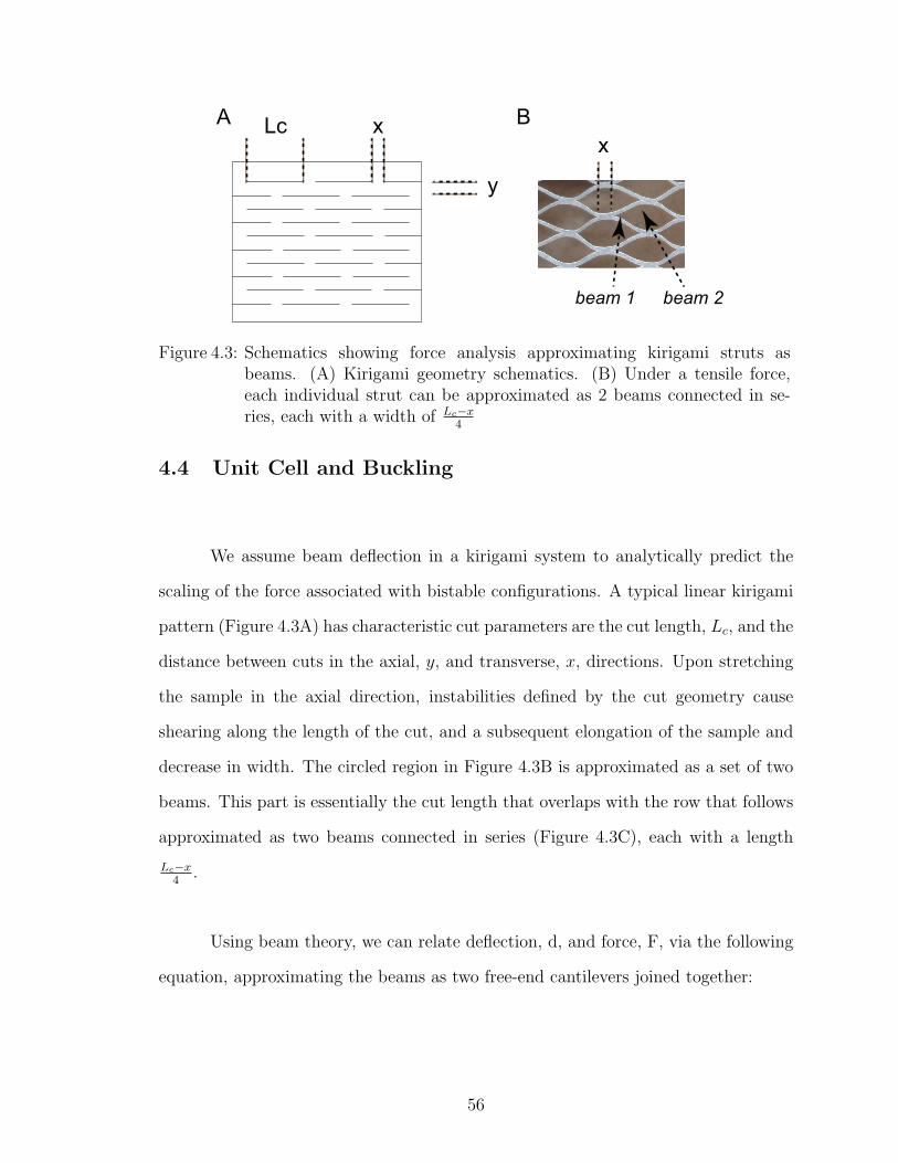
LcA x
y
B
x
beam 1 beam 2
Figure 4.3: Schematics showing force analysis approximating kirigami struts asbeams. (A) Kirigami geometry schematics. (B) Under a tensile force,each individual strut can be approximated as 2 beams connected in se-ries, each with a width of Lc−x
4
4.4 Unit Cell and Buckling
We assume beam deflection in a kirigami system to analytically predict the
scaling of the force associated with bistable configurations. A typical linear kirigami
pattern (Figure 4.3A) has characteristic cut parameters are the cut length, Lc, and the
distance between cuts in the axial, y, and transverse, x, directions. Upon stretching
the sample in the axial direction, instabilities defined by the cut geometry cause
shearing along the length of the cut, and a subsequent elongation of the sample and
decrease in width. The circled region in Figure 4.3B is approximated as a set of two
beams. This part is essentially the cut length that overlaps with the row that follows
approximated as two beams connected in series (Figure 4.3C), each with a length
Lc−x4
.
Using beam theory, we can relate deflection, d, and force, F, via the following
equation, approximating the beams as two free-end cantilevers joined together:
56

d =FL3
3EI
where L is the beam length, E the Youngs modulus of the material, and I the moment
of inertia, where
I =wt3
12
Here w is the width of the beam, and t the thickness in the direction of
deflection. It follows that
d =4FL3
Ewt3
Since the two beams are connected in series, the deflection is additive such
that
dtotal = dbeam1 + dbeam2 = 2dbeam1 =8FL3
Ewt3
Solving for force as a function of deflection, and substituting the kirigami unit
cell parameters,
Fbeam =Eyt3
4(Lc−x4
)3=
8Edyt3
(Lc − x)3
57

The total force acting on the kirigami structure is thus a sum of all the beams
in the transverse direction (i.e. along the width of sample) and axial direction (i.e.
along the length of sample). The beams in a given row are connected in parallel such
that the forces acting on the structure for that row are additive, thus the total force,
Ftotal, can be expressed in terms of force on a row Frow, number of row Nrow, and the
previously defined terms:
Ftotal =Frow
Nrow
=NBFbeam
Nrow
=8dNBEyt3
Nrow(Lc − x)3
The maximum extension, or attainable strain (in % strain) is the ratio between
the change of length at maximum extension to the original length:
%strain =∆L
Li
=Lc − x
2y
Once this maximum is reached, the final yielding will vary based on how the
cuts grow.
The effect of the kirigami pattern on the overall mechanical response can be
evaluated using the same beam assumption, and we find that the critical force scales
with Eyt3
(Lc−x)3. This buckling analysis gives us an intuition on how the experimental
parameters relate to the critical buckling force. It is, however, not trivial to predict
the force-displacement relationships, or the elastic response due to the complex de-
formation that also involve twisting and bending. Here, FEM is useful to predict the
post-buckling behavior.
58
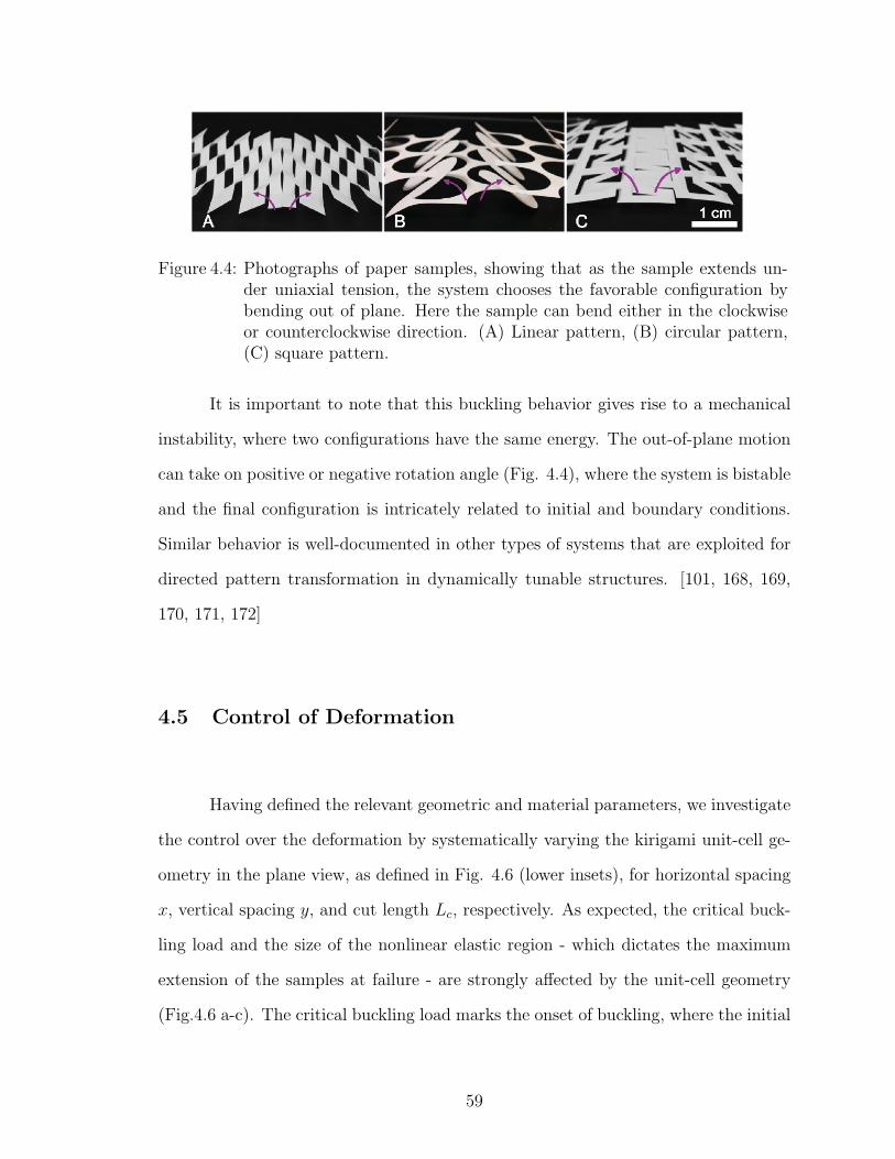
Figure 4.4: Photographs of paper samples, showing that as the sample extends un-der uniaxial tension, the system chooses the favorable configuration bybending out of plane. Here the sample can bend either in the clockwiseor counterclockwise direction. (A) Linear pattern, (B) circular pattern,(C) square pattern.
It is important to note that this buckling behavior gives rise to a mechanical
instability, where two configurations have the same energy. The out-of-plane motion
can take on positive or negative rotation angle (Fig. 4.4), where the system is bistable
and the final configuration is intricately related to initial and boundary conditions.
Similar behavior is well-documented in other types of systems that are exploited for
directed pattern transformation in dynamically tunable structures. [101, 168, 169,
170, 171, 172]
4.5 Control of Deformation
Having defined the relevant geometric and material parameters, we investigate
the control over the deformation by systematically varying the kirigami unit-cell ge-
ometry in the plane view, as defined in Fig. 4.6 (lower insets), for horizontal spacing
x, vertical spacing y, and cut length Lc, respectively. As expected, the critical buck-
ling load and the size of the nonlinear elastic region - which dictates the maximum
extension of the samples at failure - are strongly affected by the unit-cell geometry
(Fig.4.6 a-c). The critical buckling load marks the onset of buckling, where the initial
59

elastic linear regime transitions to the nonlinear regime. Our experimental results
show that an increase in x-spacing shifts the stressstrain curve up, corresponding to
higher critical buckling loads. An increase in y-spacing decreases the maximum exten-
sion and increases the critical buckling load, as expected from the beam analysis. An
increased Lc softens the material, resulting in a lower critical buckling load and higher
extensibility. Generally, an increased spacing between the cuts makes the sheet more
rigid and imparts a higher critical buckling load, whereas increasing the cut length
weakens the material, lowers its critical buckling load, and increases its extensibility.
In contrast to the usual trade-off between strength and extensibility, an increased
x-spacing does not exhibit this trade-off. This is because each cut is able to grow,
or tear, along the cut length until neighboring (in the strain-transverse direction)
cuts begin to coalesce, without the overall structure failing. In the process of tearing
and final coalescence along the cuts, fracture energy is dissipated while allowing the
sheet to extend even further. Hence, the increase of toughness here is related to the
distance between the structural features, demonstrating a toughening strategy on a
higher length scale. This suggests that the relationship between pattern spacing and
mechanical response may be extended to other length scales and materials where high
strains are desirable. The uniformity of the material is the only structural limitation
for such scaling behavior that we foresee at present. The cuts need only to be larger
than the typical variations in materials composition and properties of the sheet.
The key trends observed in our experiments are replicated by FEM analysis
(Fig. 4.6ac insets), revealing geometric parameters that are in agreement with our
intuitive understanding and the beam deflection analysis. We note that FEM accu-
rately reproduces the general stressstrain response and the experimentally observed
effects of geometrical parameters. Conversely, FEM predictions underestimate the
buckling load. These deviations are associated with microscale deformations of the
60

Figure 4.5: SEM images showing the morphology of (A) the paper sample and (B)the polyimide sample.
material. For example, the finite-element model does not describe the fibrous mor-
phology observed in typical paper samples (Fig. 4.5A). However, it is possible to
use a uniform polyimide sample that does not have the fibrous morphology, which
reflect quantitative agreement with between FEM and experimental data (Fig. 4.5B).
Confirming the source of the deviations, we achieved quantitative agreement with our
experiments by using a uniform crystalline polyimide film, laser-cut to render clean,
even widths. These samples were also tested for fatigue life up to 1,000 cycles running
to 70% strain, with an 18% strain energy fade. [173, 174] This result shows remarkable
damage tolerance and suggests potential reversible and reconfigurable applications for
the kirigami patterns.
The FEM results show that the applied load is distributed uniformly through-
out the kirigami sheets, rather than concentrating on singularities with random initi-
ation sites (Fig.4.7).Thus, highs train is accommodated to improve damage tolerance
despite multiple defect sites. This deformation scheme contrasts with the deformation
of typical stiff materials, where the presence of any defect acts as a stress concentra-
tor from which cracks propagate and lead to fracture. Considering the deformation
in terms of stress fields, we find that kirigami patterns can be used to dictate stress
concentrations and effectively control deformation. To further reduce the loads at the
61

Strain (%)
(a) (b) (c) S
tre
ss
(P
a)
increase x increase y increase Lc
FEM FEM FEM
Figure 4.6: Experimental and FEM-calculated stress-strain curves for macroscalekirigami sheets with variable unit-cell parameters. (a) Horizontal sep-aration x bewteen the cuts. (b) Vertical separation y between the cuts.(c) Cut length Lc. Figures show the experimental results and insets showresults from FEM.
cuts, we employ a technique widely used in fracture mechanics - blunting the crack tip
using a stress distributing geometry, such as circles (Fig.4.8). These circular features
effectively delay the onset of tearing and lead to a larger operating window for the
nonlinear elastic region.
62
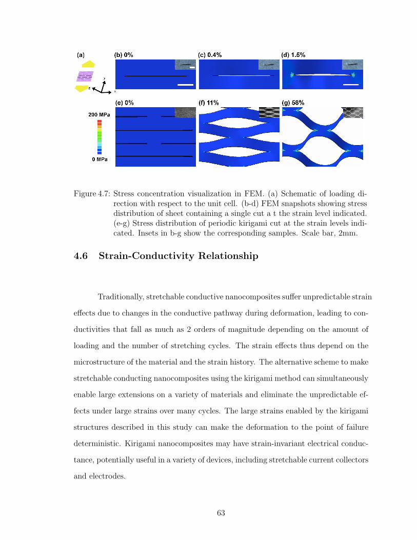
Figure 4.7: Stress concentration visualization in FEM. (a) Schematic of loading di-rection with respect to the unit cell. (b-d) FEM snapshots showing stressdistribution of sheet containing a single cut a t the strain level indicated.(e-g) Stress distribution of periodic kirigami cut at the strain levels indi-cated. Insets in b-g show the corresponding samples. Scale bar, 2mm.
4.6 Strain-Conductivity Relationship
Traditionally, stretchable conductive nanocomposites suffer unpredictable strain
effects due to changes in the conductive pathway during deformation, leading to con-
ductivities that fall as much as 2 orders of magnitude depending on the amount of
loading and the number of stretching cycles. The strain effects thus depend on the
microstructure of the material and the strain history. The alternative scheme to make
stretchable conducting nanocomposites using the kirigami method can simultaneously
enable large extensions on a variety of materials and eliminate the unpredictable ef-
fects under large strains over many cycles. The large strains enabled by the kirigami
structures described in this study can make the deformation to the point of failure
deterministic. Kirigami nanocomposites may have strain-invariant electrical conduc-
tance, potentially useful in a variety of devices, including stretchable current collectors
and electrodes.
63

Strain (%)
Str
es
s (
Pa
) FEM
0 MPa
200 MPa
Figure 4.8: Blunting the cut edge in the form of a circle at the edge of the cuts canfurther distribute the stress at each cut edge. The plot shows the samplewith (red) and without (black) the stress distributing geometry. Theeffective stress at the crack tip decreases, as seen in the FEM insets.
64

a
500 nm 500 nm
b
Figure 4.9: SEM images showing the microstructure of CNT nanocomposite on (a)paper, fabricated by vacuum infiltration, and (b) on parylene, fabricatedby LBL.
The large strains enabled by the kirigami structures described in this study
may have strain-invariant electrical conductance, potentially useful in a variety of
devices, including stretchable current collectors and electrodes. To do so, we infil-
trate tracing paper with well-dispersed single-walled carbon nanotubes. Kirigami
patterning is similarly introduced on the CNT infiltrated paper. For comparison, an
LBL-assembled (CNT/PVA)30 was fabricated on a 5-m parylene. (Fig. 4.9)With the
kirigami patterns, the yield strain increases from around 5% to 290% and 200% for
the paper and LBL nanocomposite, respectively. The conductance does not change
significantly during stretching for both the paper and LBL nanocomposites (Fig.
4.11b), indicating that the presence of the patterned notches accommodates strain
while maintaining a conductive network provided by the CNT. In both cases the
strain obtained is 20-30 times greater than for similar composites without the notch
patterns. [175]
The unique combination of high strain and high conductivity observed for 3D
kirigami nanocomposites allows us to use them as electrodes for tunable plasma dis-
charge inside an argon-filled glass tube. We use a custom glass plasma chamber (Fig.
65

4.10). The top is fitted with a hollow glass tube to allow for in situ strain tuning
capabilities while the voltage is applied onto the kirigami electrode. The ground is
attached on one side of the glass chamber for observation of changes in plasma dis-
charge under different strain levels. At constant voltage and pressure, the electric
field concentrates at the sharp apices that arise from the strain-induced out-of-plane
deformation (Fig. 4.11c). At constant voltage and pressure, the electric field concen-
trates at the sharp apices that arise from the strain-induced out-of-plane deformation.
Effectively, the increased strain increases the roughness of the electrode, which lowers
the corona onset voltage. [176] Hence, as the strain level is increased, we visually ob-
serve a higher degree of local ionization and plasma intensity resulting from increased
recombination of ionized species. The development of tunable electrodes opens up the
possibility of many useful new applications in plasma materials treatment, processing,
deposition, plasma induced airflow, and more.
66

Figure 4.10: Schematics of the custom-made plasma chamber, with in-situ tunablestrain, argon inlet, vacuum outlet, and an RF transformer to apply thevoltage.
67

Figure 4.11: Strain-invariant conductance on CNT nanocomposites as an electrode.(a) Scanning electron micrograph of CNT nanocomposite sheet made byvacuum infiltration. (b) Kirigami pattern introduced on a CNT infil-trated paper. (c) Conductance versus strain data for kirigami on paper(infiltrated CNT) and LBL on parylene, and (d) Plasma patterns gener-ated on a krigami electrode at strain levels of 5, 10, 15, 20, and 25% (leftto right); upper and lower insets show front and side views, respectively.(b, d) Scale bars, 1 cm.
And finally, we tested the kirigami samples by cyclically loading nanocomposite
paper to 200% strain over 4 cycles, and a polyimide sample to 60% strain over 1000
cycles (Fig. 4.12). In the nanocomposite paper, we see elastic energy recovery of
75% on the first run, and around 90% on the subsequent runs. It appears that the
in the first run, some elastic energy is not recoverable due to permanent deformation
occurring on the microstructural level. The polyimide sample experiences a fall in
recoverable energy (the area under the stress-strain curve) in the first 100 cycles. As
the number of cycle increases, the recoverable strain energy appears to flatten out.
For use in a practical device, some of the critical design parameters for a cyclically
loaded kirigami device will include the total deforming area, which will have to do
with the fraction of the overall area undergoing deformation, and the thickness of the
68

film, which will determine the recoverable bending radius. More mechanical fatigue
data will further elucidate how the kirigami patterning influences fatigue life. Other
designs of kirigami that allow multi-directional loading and the cut edge blunting
strategy mentioned previously can also be an effective ways to widen the applicability
of kirigami patterning.
4.7 Conclusion
In this chapter we have presented a framework to directly design deformation
within a nanocomposite and delocalize stress distribution using the kirigami pattern-
ing technique and thus eliminating the unpredictable strain effects in nanocomposites.
We also demonstrate the combination of the control of component in nanocomposite
and its architecture via kirigami. This strategy allows us to have strain-invariant con-
ductance within the material over a range of strain up to several times the ultimate
strain of the material, depending on the cut geometry.
In contrast to molecular or nanoscale manipulation of strain, we show that it is
possible to control deformation in materials with top-down kirigami patterning, which
can be extended tom ultiple length scales. The new insights obtained here may bridge
the gap between nanoscale and macroscale strain engineering, as well as enable novel
engineering applications in which out-of-plane deflection can be controlled to create
multiscale, reconfigurable structures. Kirigami nanocomposites may find potential
use in radio-frequency plasma applications, including surface treatment, materials
processing, displays, radar phase arrays, ozone production and corona-induced air-
flow. Deformable electrodes that can withstand a wide range of strains can also be
extended to a variety of flexible-electronic technologies beyond plasma processes.
69

Figure 4.12: Cyclic loading data for the nanocomposite paper and polyimide, showingelastic energy recovery. (A) Nanocomposite paper tested over 4 cycles,and (B) polyimide sample tested over 1000 cycles, plotting the recoveredstrain energy versus cycle number. Inset, the stress-strain data from thefirst to 1000th cycle.
70

CHAPTER V
Tunable Kirigami
In the previous chapter we have described kirigami patterned structures and
proposed using kirigami as a way to engineer elasticity and deformation. In this
chapter we focus on how to use these kirigami patterned structures for dynamic
applications. Recent development in kirigami has fueled research interest in using
these mechanical structures for dynamic purposes, including solar tracking [174] and
optical transmission window. [177]
We propose applying the kirigami approach to explore the dynamic tuning of
radio frequency (RF) plasma because of two primary reasons. The first is that the
phenomenon is visible, making the observation convenient - within a plasma, inelastic
collisions occur to emit radiation of light. The second is that dynamic applications
can have profound technological significance when applied to plasma processes, and
demonstration of dynamic tuning will have significant impact in a myriad of materials
processing methods currently employed in industry. With the recent development on
plasma actuators to control airflow around aerodynamic surfaces, it is anticipated
that kirigami electrodes may find critical applications there. We conclude with a few
remarks on some foreseeable future directions in tunable kirigami.
71

5.1 Background
A plasma is a quasi-neutral ionized gas system containing equal number den-
sities of electrically charged constituents, which are electrons and ions. The term
plasma was first introduced by Langmuir [178] in 1927 to describe the gaseous fluid
carrying electrons and ions, for its similarity to how plasma in blood carries the
various blood cells. During excitation, a plasma is sustained by electron-neutral dis-
sociative ionization. Within a plasma, the electrons move much faster compared to
the ions and collide with one another as they move around in space. During this
process, either elastic or inelastic collision can occur. Elastic collisions lead to energy
transfer and dissipation but the total kinetic energy remains the same:
Ar0 + e− → Ar0 + e−.
In contrast, inelastic scattering is responsible for excitation
e+ Ar → Ar∗ + e
or electronic transitions
Ar+ + e− → Ar∗ + e → Ar + e+ hν
corresponding to
3p6 → 3p54s1.
Here, positive argon ion can interact with an electron and undergo an electronic
transition in the outer shell, which emits a photon with the characteristic purple
light.
72

Plasma processes have found important roles in industrial applications, partic-
ularly in electronics and materials processing, [179] as briefly alluded to in Chapter
II. Depending on the interactions between the reactive ions and the material, a
few plasma-material processes can occur, including ablation, etching, deposition, or
chemical and physical modification due to particles and radiation from the plasma.
These effects have sustained the production high powered integrated circuits, further
underscoring the importance of these controlled processes.
Hence, by investigating the effects of strain tuning of a kirigami electrode in
a plasma system, we can visualize the effects easily and there is a number of indus-
trial applications associated with tunable plasma electrodes. Further, the plasma
parameters can be quantified using a Langmuir probe, which measures the current at
various voltages. From the current-voltage (I − V ) characteristics, the electron and
ion currents, densities, and electron temperature can be extracted.
5.2 Experimental Method
As a first demonstration, we use a 25 µm Kapton polyimide film with e-beam
evaporated 5 nm Cr and 50 nm Au for electrical conductivity and contact between
the film and the chuck in a radio frequency (RF) plasma generator. The kirigami
pattern is introduced using a laser cutting tool (WKLaser LC1280) at 40 W, the cut
spacings at 2 mm and Lc at 1 cm.
At a frequency of 13.56 MHz, using argon gas at 500 mTorr and 50 W, we are
able to sustain a plasma. The strain level on the kirigami sample is varied from 0%
strain to 20% strain. The I − V curves are obtained at each strain level, averaged
73

over 5 times. The bulk plasma parameters are automatically extracted.
5.3 Strain-Tunable Plasma Parameters
The extracted plasma parameters show increase of number and current density
for both the ions and the electrons within the plasma with increasing strain. At higher
strain levels, the localization of electric field on the sharp edges in the kirigami sample
tends to cause severe arcing, which can damage the sample. At higher strains, the
plasma tends to be also unstable. However, it can be seen qualitatively (Fig. 5.1)
and quantitatively (Fig. 5.2) that the tuning of electric field due to the change in
topology can induce changes in bulk plasma properties.
Typically to tune these properties, one can change the RF power and gas
pressure. It is conceivable that fine tuning the geometry, length scale, and operating
power, one can use mechanical strain as a knob to tune bulk plasma properties.
Additionally, the local electric field is inversely related to the radius of curvature.
The radius of curvature decreases as the strain is increased. Therefore, the strain-
tuning of kirigami can effectively alter the local electric field due to the out-of-plane
deformation, and in turn modulate the power density of the plasma, and concentrate
the electric field at the sharp electrode edges.
74

Figure 5.1: Qualitative data showing stress-tunable plasma properties at strain levelsof 0, 5, 10, and 16%.
75
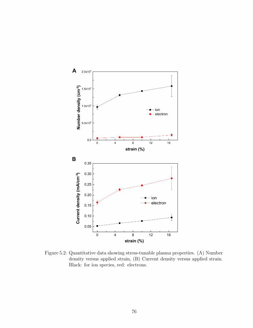
Figure 5.2: Quantitative data showing stress-tunable plasma properties. (A) Numberdensity versus applied strain, (B) Current density versus applied strain.Black: for ion species, red: electrons.
76

5.4 Conclusion
We have shown that it is possible to tune bulk plasma properties by altering
the local electric field. Besides the number density and current density of the charged
species, the spatial and temporal structure of the plasma will can be further explored
for the emerging application in, for example, aerodynamic plasma actuator. Recent
interest in dielectric barrier discharge plasma has been focused on aerodynamic ap-
plications. The plasma discharge strongly influences the surrounding airflow, and
can be used to control aerodynamic surfaces without the use of mechanical parts.
[180, 181, 182]
Beyond plasma parameters, it is also possible to use the kirigami technique to
design chiral materials. The subject is outside the scope of this thesis, however, it
is worth briefly noting the literature on kagome [183] and auxetic lattices. [184, 171]
Certain cellular lattices and the kagome lattice - a tiling pattern in woven basketry
and certain crystal structures - are capable of chiral transitions from rotation. An
example of the chiral kirigami design is illustrated (Fig. 5.3). More on the design and
mechanics of these rotating structures will need to be investigated for application of
kirigami chiral materials.
77

Figure 5.3: Rotating kirigami structures with out-of-plane twists.
78
CHAPTER VI
Summary and Future Directions
The field of engineering origami and kirigami has a relatively short history, and
is a rapidly developing area. Balanced by geometry, the potential for reconfigurability
sits in the intersection between materials and mechanics. Since the early studies on
deployable structures for aerospace applications by Miura [3, 4] and others, [16] re-
search in engineering foldable and morphing structures have translated into diverging
and fruitful areas, including 3D microfabrication, bio-mimicry, and metamaterials.
In this work, we have focused on composite systems and described coupling
materials and mechanics to engineer functionalities. In Chapter III, we described
an approach to create a layer-by-layer assembled humidity-responsive mechanical ac-
tuator. Electrostatically held water can reversibly go in and out of the system. A
bilayer scheme is employed, where the differential response between the two layers
with changes in ambient humidity effectively helps us create gentle mechanical motion
on the order of seconds in response time. Additionally, inkjet patterning allows us to
place the active material precisely in space. In Chapters IV and V, we described an
approach to control strain-property relationship by controlling the deformation via
kirigami patterning. In materials engineering, one typically tunes properties of mate-
79

rials by atomic and microstructural manipulation; here we show that the deformation
of the material is controlled by the geometry to enable functionality.
Besides the mechanistic design rules and the materials involved, smart materi-
als of the future using these strategies would also require considerations of scale, both
in time and in space. The response time, τ , for example, will influence how materials
are being used, beyond the start and end states. The response time may also be a
function of the length scale in question. Future studies can be guided by thinking
about the time scale and length scale of responsiveness. These will determine what
kinds of applications are possible. In the following sections, we discuss future work in
the context of time scale and length scale. Finally, we will conclude with a discussion
on the design of deformation.
6.1 Time Scale
In nature, the origami folding scheme based on hydration is also seen in
pinecones, wheat awn, and many seed dispersal systems. [185, 186, 187] Bilayers of
materials with different swelling properties controls the hydroscopic actuators, much
like in a thin bimetallic metal strip. [48] These systems are entirely driven by the am-
bient humidity and do not require electrical control, making them suitable for passive
design elements driven by environmental changes.
The gentle movement due to multilayer hydration is in contrast to the fast
movement observed in the Venus fly trap. The response time on the order of 102
milliseconds is possible because of a buckling bistability, where the structure has
two mechanically stable configurations. Holmes and Crosby [169] investigated the
80

response time by mimicking the Venus fly trap with PDMS, an elastomeric material.
Much like many systems described in this work and in the referenced literature,
the mechanical instability is a balance between materials properties and geometry.
Similar to bilayer bending, buckling is also dependent on the material thickness (t)
and Youngs modulus (E), and thus the system can be scaled up to larger systems
(meter scale) and down (micro- to nanometer scale). Here, τ is given by:
τ ≈ µt2
kE
where µ is the viscosity of the swelling fluid in the system, and k is the hy-
draulic permeability, for a buckling shell encapsulating a fluid-filled cell. This example
demonstrate using mechanical instability to control the response time in a responsive
system.
Important to note, however, for bilayer bending schemes described in these
studies, the processes are controlled by diffusion (of ions, [31] water, [140] or heat
[132]). In this case, microscale actuators works well, but for larger scale systems, the
transport pathway will have to be engineered. Hence the length scale must be given
consideration for successful design.
6.2 Length Scale
In contrast to the length scale dependency in transport phenomena, in ge-
ometric systems the length scale independence of the governing physical laws can
81

make them suitable for the development of mechanical metamaterials. In creating
stimuli responsive materials, the consideration of length scale is also related to how
the structure is actuated and the resulting application. In the integrated circuits
world, reducing in length scale relate to profit. In contrast, in the world of responsive
systems, length scale tells us which functional properties can be controlled. For ex-
ample, in the macroscale, kirigami has recently been demonstrated for solar tracking
application. [174] In the sub-millimeter scale, the kirigami technique combined with
strained polymer has been used to organize microarrays. [177] These are relatively
new studies. In Chapter IV, we have discussed controlling microscale deformation to
maintain conductance throughout the entire range of strain. This is one example of
how the control of deformation at a specific length scale can help control functional
properties. Ongoing work in this area can extended to sub-micron scales and smaller,
with application in the control of optical properties, including chiral materials and
diffraction gratings.
Mechanical instability is intricately related to geometry. Over the years, the
Bertoldi group has studied a range of architectured shell structures with negative
Poisson’s ratio in the form of sheets and buckling three-dimensional structures termed
“Buckliballs”. [101, 188, 189] Similar to the Miura-ori, the mechanical properties arise
primarily from the geometry. Experimental demonstrations are typically silicone-
based elastomers and hydrogels because of the ease of fabrication - usually by a
molding process - and reversibility. Future work in incorporating nanomaterials can
potentially couple the well-described mechanics with other functional properties in
various length scales and time scales, and is expected to have important implications
in smart material systems. [190]
82

6.3 Design of Deformation
Further, designing deformation via kirigami as we have discussed in Chapter
IV has potential applications in engineering mechanical properties and extending the
fatigue life of stretchable devices. For example, we have described in Chapter I that
microfabricated biomedical devices have seen tremendous growth in recent years. One
critical materials challenge in this area is on matching the mechanical property of de-
vice with that of tissues, while maintaining functionality. This is especially important
for implants in the brain - a neural probe may be inserted within the brain, but mis-
matched mechanical properties between the probe and the tissue would cause chronic
inflammation despite otherwise minimal biological response. Typically, tissues have
Young’s modulus (E) on the order of kPa, while microfabricated silicon electrodes are
on the order of GPa. Currently, to overcome this problem, several studies have looked
into creating thin structures supported on flexible substrates. [50] These structures
are typically buckled, [163] serpentine, [191, 192] or hierarchical, [165] and it is also
possible to directly evaporate thin metal films onto flexible substrates. By using the
kirigami approach, one can anticipate engineering the desired mechanical response
directly into the material. Because of the structural deformation, it is possible to
accommodate strains and minimize strain effects typically observed in stretchable
conducting nanocomposites. Using computational modeling, it is expected that a
range of geometries and desired mechanical response can be quickly explored.
Focusing on the design of deformation, the kirigami approach described in this
work can be thought of as a two dimensional case to design deformation pathway,
enabled by buckling out of plane. Extrapolating this design strategy to a three-
dimensional case, architectured materials such as microlattices [193, 194, 195, 196,
197] also demonstrate a pathway to design the mode of deformation under a compres-
83

sive mechanical load. Typically, metallic and ceramic microlattices are fabricated by
uniformly coating a template constructed using two-photon lithography direct laser
writing. The template is later removed, leaving the hollow microlattices. Because
of the structural hierarchy from the centimeter to nanometer scale, metal microlat-
tices are capable of complete recovery of compressive load. More recently, ceramic
microlattices have also been made by atomic layer deposition (ALD) or sintering of
nanoparticle-loaded resins. [194] Whereas ceramic materials typically suffer catas-
trophic brittle failure, the microlattice architecture effectively control the deforma-
tion mode, resulting in materials that can withstand recoverable 50% compressive
load. Studies on cellular solids highlight using the lattice structures such as octet-
truss to control the deformation mechanism, which result in their high strength. The
lightweight, high strength, and elastic recovery afforded by the AM microlattices are
desirable for material designs that go through cyclic loads.
In both the 2D kirigami and the 3D microlattice examples, the periodic struc-
tures give rise to the control of the deformation, such that stresses concentrate at
designated spatial positions, as opposed to stochastically distributed defects and
voids. Periodic and architectured structures offer an approach to engineer the de-
formation mechanism, such that two goals can be realized. The first is that these
structures have desirable strength-to-weight ratio. The second is that the hierar-
chical structuring can enable control of deformation mechanism and recovery in the
brittle materials. Anticipated relevant parameters include thickness-to-width ratio of
the deforming members, scales of hierarchy, and geometry. Also expected is that the
control of deformation established by computation and confirmed by experiment can
provide rational design of novel architectured materials that operate within the range
of the engineered deformation.
84

Finally, in conjunction with the design of deformation, kirigami and origami en-
gineering have been of research interest because the possibility to create out-of-plane
deformation, or the “pop-up” effect. Driven by the minimization of strain energy,
buckling deformation seen in kirigami, wrinkling observed in hard skin on flexible
substrate, and self-positioning of bilayers are all examples of deformation in the third
dimension. Engineering of the pop-up effect on multiple length scales is expected to
have applications in aerodynamic skin, pattern transformation, and surface engineer-
ing. Continued growth in engineering origami and kirigami can be anticipated. The
time and length scale will need to be taken in consideration along with the mechanics
of deformation. Designing deformation will yield an effective engineering approach
toward next generation of tunable and multifunctional materials.
85

BIBLIOGRAPHY
86

BIBLIOGRAPHY
[1] Thomas Francis Carter. The invention of printing in China and its spreadwestward. The Ronald Press Company, New York, 2nd edition, 1955.
[2] Unknown. Hiden senbazuru orikata. Japan, 1797.
[3] K Miura. Proposition of Pseudo-Cylindrical Concave Polyhedral Shells. Insti-tute of Space and Aeronautical Science Report, pages 141–163, 1969.
[4] K Miura. PCCP Shell. In H.R. Drew and S. Pellegrino, editors, New Approachesto Structural Mechanics, Shells, and Biological Structures. Springer Science,2002.
[5] Yutaka Nishiyama. Miura folding: applying origami to space exploration. In-ternational Journal of Pure and Applied Mathematics, 79(2):269–279, 2012.
[6] Ramses V. Martinez, Carina R. Fish, Xin Chen, and George M. Whitesides.Elastomeric Origami: Programmable Paper-Elastomer Composites as Pneu-matic Actuators. Advanced Functional Materials, 22(7):1376–1384, apr 2012.
[7] D. H. Gracias, J Tien, T. L. Breen, C Hsu, and George M. Whitesides. FormingElectrical Networks in Three Dimensions by Self-Assembly. Science, 289:1170–1172, 2000.
[8] Jose M. Zanardi Ocampo, Pablo O Vaccaro, Thomas Fleischmann, Te-shengWang, Kazuyoshi Kubota, Tahito Aida, Toshiaki Ohnishi, Akira Sugimura,Ryo Izumoto, Makoto Hosoda, and Shigeki Nashima. Optical actuation of mi-cromirrors fabricated by the micro-origami technique. Applied Physics Letters,83(18):3647, 2003.
[9] Timothy G Leong, Paul A Lester, Travis L Koh, Emma K Call, and David HGracias. Surface tension-driven self-folding polyhedra. Langmuir, 23(17):8747–8751, 2007.
[10] Z. Y. Wei, Z. V. Guo, L. Dudte, H. Y. Liang, and L. Mahadevan. Geometric Me-chanics of Periodic Pleated Origami. Physical Review Letters, 110(21):215501,may 2013.
[11] Toen Castle, Yigil Cho, Xingting Gong, Euiyeon Jung, Daniel M. Sussman,Shu Yang, and Randall D. Kamien. Making the Cut: Lattice Kirigami Rules.Physical Review Letters, 113(24):245502, dec 2014.
87

[12] Kazuya Saito, Akira Tsukahara, and Yoji Okabe. New Deployable Struc-tures Based on an Elastic Origami Model. Journal of Mechanical Design,137(2):021402, feb 2015.
[13] By Thomas W Ebbesen and Hidefumi Hiura. Graphene in 3-Dimensions :Towards Graphite Origami. Advanced Materials, 7(6):582–586, 1995.
[14] Steven Cranford, Dipanjan Sen, and Markus J Buehler. Meso-origami: Foldingmultilayer graphene sheets. Applied Physics Letters, 95(12):123121, 2009.
[15] Melina Blees, Peter Rose, Arthur Barnard, Samantha Roberts, and Paul L.McEuen. Graphene Kirigami, 2014.
[16] Tomohiro Tachi. Generalization of Rigid Foldable Quadrilateral Mesh Origami.Proceedings of the International Association for Shell and Spatial Structures(IASS) Symposium, (October):2287–2294, 2009.
[17] Erik D Demaine. Folding and Unfolding Linkages, Paper, and Polyhedra. Re-vised Papers from the Japan Conference on Discrete and Computational Geom-etry2, 2098:113–124, 2000.
[18] Mark Schenk and Simon D Guest. Geometry of Miura-folded metamaterials.Proceedings of the National Academy of Sciences of the United States of Amer-ica, 110(9):3276–81, feb 2013.
[19] Robert J. Lang. A computational algorithm for origami design. Proceedingsof the twelfth annual symposium on Computational geometry - SCG ’96, pages98–105, 1996.
[20] Robert Lang and Thomas Hull. Origami design secrets: mathematical methodsfor an ancient art. Springer, 27:92–95, 2002.
[21] J. L. Silverberg, A.A. Evans, L. McLeod, R. C. Hayward, T. Hull, C. D. San-tangelo, and I. Cohen. Using origami design principles to fold reprogrammablemechanical metamaterials. Science, 345(6197):647–650, aug 2014.
[22] Jesse L Silverberg, Jun-hee Na, Arthur a Evans, Bin Liu, Thomas C Hull,Christian D Santangelo, Robert J Lang, Ryan C Hayward, and Itai Cohen.Origami structures with a critical transition to bistability arising from hiddendegrees of freedom. Nature Materials, (March):1–5, 2015.
[23] Shivendra Pandey, Margaret Ewing, Andrew Kunas, Nghi Nguyen, David HGracias, and Govind Menon. Algorithmic design of self-folding polyhedra. Pro-ceedings of the National Academy of Sciences of the United States of America,108(50):19885–90, dec 2011.
[24] R. P. Feynman. There’s plenty of room at the bottom. Engineering and Science,23(5):22–36, 1960.
88

[25] H.C. Nathanson, W.E. Newell, R.A. Wickstrom, and Jr. Davis, J.R. The res-onant gate transistor. IEEE Transactions on Electron Devices, 14(3):117–133,1967.
[26] K.P. Rajurkar, G. Levy, a. Malshe, M.M. Sundaram, J. McGeough, X. Hu,R. Resnick, and a. DeSilva. Micro and Nano Machining by Electro-Physicaland Chemical Processes. CIRP Annals - Manufacturing Technology, 55(2):643–666, 2006.
[27] S.M. Sze. Semiconductor devices: physics and technology. John Wiley & Sons,2001.
[28] Vikas Choudhary and Krzysztof Iniewski. MEMS: Fundamental Technology andApplications. CRC Press, 2013.
[29] E Smela, O Inganas, and I Lundstrom. Controlled folding of micrometer-sizestructures. Science (New York, N.Y.), 268(5218):1735–8, jun 1995.
[30] Silas Alben, Bavani Balakrisnan, and Elisabeth Smela. Edge effects determinethe direction of bilayer bending. Nano letters, 11(6):2280–5, jun 2011.
[31] E W Jager, E Smela, and O Inganas. Microfabricating conjugated polymeractuators. Science (New York, N.Y.), 290(5496):1540–5, nov 2000.
[32] Alexander Vorob’ev, Pablo Vaccaro, Kazuyoshi Kubota, Shanmugam Sara-vanan, and Tahito Aida. Array of Micromachined Components Fabricated UsingMicro-Origami Method. Japanese Journal of Applied Physics, 42(Part 1, No.6B):4024–4026, jun 2003.
[33] Scott T. Brittain, Olivier J. A. Schueller, Hongkai Wu, Sue Whitesides, andGeorge M. Whitesides. Microorigami: Fabrication of Small, Three-Dimensional,Metallic Structures. The Journal of Physical Chemistry B, 105(2):347–350, jan2001.
[34] Yingkai Liu, Lance Oh, S. Fanning, B. Shapiro, and E. Smela. Fabricationof folding microstructures actuated by polypyrrole/gold bilayer. In TRANS-DUCERS ’03. 12th International Conference on Solid-State Sensors, Actuatorsand Microsystems. Digest of Technical Papers (Cat. No.03TH8664), volume 1,pages 786–789. IEEE, 2003.
[35] Kazuyoshi Kubota, Thomas Fleischmann, Shanmugam Saravanan, Pablo O.Vaccaro, and Tahito Aida. Self-Assembly of Microstage Using Micro-OrigamiTechnique on GaAs. Japanese Journal of Applied Physics, 42(Part 1, No.6B):4079–4083, jun 2003.
[36] Pablo O Vaccaro, K Kubota, T Fleischmann, S Saravanan, and T Aida. Valley-fold and mountain-fold in the micro-origami technique. Microelectronics Jour-nal, 34(5-8):447–449, 2003.
89
[37] E.E. Hui, R.T. Howe, and M.S. Rodgers. Single-step assembly of complex 3-Dmicrostructures. Proceedings IEEE Thirteenth Annual International Conferenceon Micro Electro Mechanical Systems (Cat. No.00CH36308), m:602–607, 2000.
[38] Paul Stellman, Tilman Buchner, William J. Arora, and George Barbastathis.Dynamics of Nanostructured Origami. Journal of Microelectromechanical Sys-tems, 16(4):932–949, 2007.
[39] Fabio Fachin, Stefan a. Nikles, and Brian L. Wardle. Mechanics of out-of-plane MEMS via Postbuckling: Model-experiment demonstration using CMOS.Journal of Microelectromechanical Systems, 21(3):621–634, 2012.
[40] Rohan Fernandes and David H Gracias. Self-folding polymeric containers for en-capsulation and delivery of drugs. Advanced drug delivery reviews, 64(14):1579–89, nov 2012.
[41] Leonid Ionov. Bioinspired Microorigami by SelfFolding Polymer Films. Macro-molecular Chemistry and Physics, pages 1178–1183, 2013.
[42] Charlotte Py, Paul Reverdy, Lionel Doppler, Jose Bico, Benoıt Roman, andCharles N. Baroud. Capillary Origami: Spontaneous Wrapping of a Dropletwith an Elastic Sheet. Physical Review Letters, 98(15):156103, apr 2007.
[43] Jeong-Hyun Cho, Teena James, and David H Gracias. Curving nanostructuresusing extrinsic stress. Advanced materials (Deerfield Beach, Fla.), 22(21):2320–4, jun 2010.
[44] Evin Gultepe, Jatinder S. Randhawa, Sachin Kadam, Sumitaka Yamanaka,Florin M. Selaru, Eun J. Shin, Anthony N. Kalloo, and David H. Gracias.Biopsy with Thermally-Responsive Untethered Microtools. Advanced Materials,25(4):514–519, jan 2013.
[45] Kate Malachowski, Mustapha Jamal, Qianru Jin, Beril Polat, Christopher JMorris, and David H Gracias. Self-Folding Single Cell Grippers. Nano Letters,14(7):4164–4170, jul 2014.
[46] Jaehyun Park, Yevgeniy V. Kalinin, Sachin Kadam, Christina L. Randall, andDavid H. Gracias. Design for a Lithographically Patterned Bioartificial En-docrine Pancreas. Artificial Organs, 37(12):1059–1067, dec 2013.
[47] GG Stoney. The tension of metallic films deposited by electrolysis. Proceedingsof the Royal Society of London. Series A, . . . , 1909.
[48] S Timoshenko. Analysis of bi-metal thermostats. J. Opt. Soc. Am, 1925.
[49] J Y Ou, E Plum, L Jiang, and N I Zheludev. Reconfigurable photonic meta-materials. Nano letters, 11(5):2142–4, may 2011.
90

[50] John A Rogers, Takao Someya, and Yonggang Huang. Materials and mechanicsfor stretchable electronics. Science (New York, N.Y.), 327(5973):1603–7, mar2010.
[51] Georgi Stoychev, Svetlana Zakharchenko, Sebastien Turcaud, John W C Dun-lop, and Leonid Ionov. Shape-programmed folding of stimuli-responsive polymerbilayers. ACS nano, 6(5):3925–34, may 2012.
[52] Srikanth Singamaneni, Michael E McConney, and Vladimir V Tsukruk.Swelling-induced folding in confined nanoscale responsive polymer gels. ACSnano, 4(4):2327–37, apr 2010.
[53] Georgi Stoychev, Nikolay Puretskiy, and Leonid Ionov. Self-folding all-polymerthermoresponsive microcapsules. Soft Matter, 7(7):3277, 2011.
[54] M. Huang, C. Boone, M. Roberts, D. E. Savage, M. G. Lagally, N. Shaji,H. Qin, R. Blick, J. a. Nairn, and F. Liu. Nanomechanical Architecture ofStrained Bilayer Thin Films: From Design Principles to Experimental Fabrica-tion. Advanced Materials, 17(23):2860–2864, dec 2005.
[55] Mustapha Jamal, Aasiyeh M Zarafshar, and David H Gracias. Differentiallyphoto-crosslinked polymers enable self-assembling microfluidics. Nature com-munications, 2:527, jan 2011.
[56] Troy R Hendricks and Iisoon Lee. Wrinkle-free nanomechanical film: Controland prevention of polymer film buckling. Nano Letters, 7(2):372–379, 2007.
[57] E Hawkes, B An, N M Benbernou, H Tanaka, S Kim, E D Demaine, D Rus,and R J Wood. Programmable matter by folding. Proceedings of the NationalAcademy of Sciences of the United States of America, 107(28):12441–5, jul 2010.
[58] Jamie K Paik, Elliot Hawkes, and Robert J Wood. A novel low-profile shapememory alloy torsional actuator. Smart Materials and Structures, 19:125014,2010.
[59] Samuel M. Felton, Michael T. Tolley, ByungHyun Shin, Cagdas D. Onal, Erik D.Demaine, Daniela Rus, and Robert J. Wood. Self-folding with shape memorycomposites. Soft Matter, 9(32):7688, 2013.
[60] Z. Tang, Y. Wang, P. Podsiadlo, and N.a. Kotov. Biomedical Applications ofLayer-by-Layer Assembly: From Biomimetics to Tissue Engineering. AdvancedMaterials, 18(24):3203–3224, dec 2006.
[61] Xiaobo Zhang, Cary L Pint, Min Hyung Lee, Bryan Edward Schubert, ArashJamshidi, Kuniharu Takei, Hyunhyub Ko, Andrew Gillies, Rizia Bardhan,Jeffrey J Urban, Ming Wu, Ronald Fearing, and Ali Javey. Optically-and thermally-responsive programmable materials based on carbon nanotube-hydrogel polymer composites. Nano letters, 11(8):3239–44, aug 2011.
91

[62] Shoji Takeuchi, Takafumi Suzuki, Kunihiko Mabuchi, and Hiroyuki Fujita. 3Dflexible multichannel neural probe array. Journal of Micromechanics and Mi-croengineering, 14:104–107, 2004.
[63] Ying Yao, Mayurachat Ning Gulari, James a. Wiler, and Kensall D. Wise. Amicroassembled low-profile three-dimensional microelectrode array for neuralprosthesis applications. Journal of Microelectromechanical Systems, 16(4):977–988, 2007.
[64] Nadrian C. Seeman. Nucleic acid junctions and lattices. Journal of TheoreticalBiology, 99(2):237–247, nov 1982.
[65] Paul W K Rothemund. Folding DNA to create nanoscale shapes and patterns.Nature, 440(7082):297–302, mar 2006.
[66] Akinori Kuzuya and Makoto Komiyama. Design and construction of a box-shaped 3D-DNA origami. Chemical Communications, (28):4182, 2009.
[67] Robert Schreiber, Susanne Kempter, Stefan Holler, Verena Schuller, DanielSchiffels, Stephanie S Simmel, Philipp C Nickels, and Tim Liedl. DNAOrigami-Templated Growth of Arbitrarily Shaped Metal Nanoparticles. Small,7(13):1795–1799, jul 2011.
[68] Robert Schreiber, Jaekwon Do, Eva-maria Roller, Tao Zhang, Verena J Schuller,Philipp C Nickels, Jochen Feldmann, and Tim Liedl. Hierarchical assemblyof metal nanoparticles, quantum dots and organic dyes using DNA origamiscaffolds. Nature Nanotechnology, 9(1):74–78, dec 2013.
[69] D Han, S Pal, J Nangreave, Z Deng, Y Liu, and H Yan. DNA Origami withComplex Curvatures in Three-Dimensional Space. Science, 332:342–347, 2011.
[70] William M Shih and Chenxiang Lin. Knitting complex weaves with DNAorigami. Current Opinion in Structural Biology, 20(3):276–282, 2010.
[71] Dongran Han, Suchetan Pal, Yan Liu, and Hao Yan. Folding and cuttingDNA into reconfigurable topological nanostructures. Nature nanotechnology,5(10):712–7, oct 2010.
[72] Melina K. Blees, Arthur W. Barnard, Peter A. Rose, Samantha P. Roberts,Kathryn L. McGill, Pinshane Y. Huang, Alexander R. Ruyack, Joshua W.Kevek, Bryce Kobrin, David a. Muller, and Paul L. McEuen. Graphene kirigami.Nature, 2015.
[73] Shuze Zhu and Teng Li. Hydrogenation-Assisted Graphene Origami and ItsApplication in Programmable Molecular Mass Uptake, Storage, and Release.ACS Nano, 8(3):2864–2872, mar 2014.
[74] Paul Zakharia Fajar Hanakata, Zenan Qi, David Campbell, and Harold Park.Highly Stretchable MoS2 Kirigami. Nanoscale, V, 2015.
92

[75] Oleg V. Yazyev and Yong P. Chen. Polycrystalline graphene and other two-dimensional materials. Nature Nanotechnology, 9(10):755–767, 2014.
[76] Steven P. Koenig, Narasimha G. Boddeti, Martin L. Dunn, and J. ScottBunch. Ultrastrong adhesion of graphene membranes. Nature Nanotechnol-ogy, 6(9):543–546, 2011.
[77] Raquel Verdejo, M. Mar Bernal, Laura J. Romasanta, and Miguel a. Lopez-Manchado. Graphene filled polymer nanocomposites. Journal of MaterialsChemistry, 21:3301, 2011.
[78] Jian Zhu, Huanan Zhang, and Nicholas A. Kotov. Thermodynamic and struc-tural insights into nanocomposites engineering by comparing two materials as-sembly techniques for graphene. ACS Nano, 7(6):4818–4829, 2013.
[79] Peng Zhang, Lulu Ma, Feifei Fan, Zhi Zeng, Cheng Peng, Phillip E. Loya, ZhengLiu, Yongji Gong, Jiangnan Zhang, Xingxiang Zhang, Pulickel M. Ajayan, TingZhu, and Jun Lou. Fracture toughness of graphene. Nature Communications,5:1–7, 2014.
[80] Zenan Qi, Harold S. Park, and David K. Campbell. Highly DeformableGraphene Kirigami. page 5, jul 2014.
[81] Peter Fratzl and Richard Weinkamer. Natures hierarchical materials. Progressin Materials Science, 52(8):1263–1334, nov 2007.
[82] MA Meyers, J McKittrick, and PY Chen. Structural biological materials: crit-ical mechanics-materials connections. Science, (February):773–779, 2013.
[83] Ray F Egerton. Physical principles of electron microscopy. Springer Science,2005.
[84] M Minsky. Microscopy Apparatus. US Patent 3013467, 3013467:5, 1961.
[85] Nathan S Claxton, Thomas J Fellers, and Michael W Davidson. Laser ScanningConfocal Microscopy. Encyclopedia of Medical Devices and Instrumentation,1979(21):1–37, 2006.
[86] Wojciech Kaplonek and Krzysztof Nadolny. Advanced 3D laser microscopyfor measurements and analysis of vitrified bonded abrasive tools. Journal ofEngineering Science and Technology, 7(6):661–678, 2012.
[87] L.R.G. Treloar. Physics of Rubber Elasticity. Oxford University Press, UK,2005.
[88] C Storm, J. J. Pastore, F. C. MacKintosh, T. C. Lubensky, and P. A. Janmey.Nonlinear elasticity in biological gels. Nature, 435(May):0–3, 2005.
93
[89] Prashant K Purohit, Rustem I Litvinov, Andre E X Brown, Dennis E Discher,and John W Weisel. Protein unfolding accounts for the unusual mechanicalbehavior of fibrin networks. Acta biomaterialia, 7(6):2374–83, jun 2011.
[90] Mary C. Boyce and Ellen M. Arruda. Constitutive Models of Rubber Elasticity:A Review. Rubber Chemistry and Technology, 73(3):504–523, jul 2000.
[91] John Gosline, Margo Lillie, Emily Carrington, Paul Guerette, Christine Or-tlepp, and Ken Savage. Elastic proteins: biological roles and mechanical prop-erties. Philosophical transactions of the Royal Society of London. Series B,Biological sciences, 357(1418):121–32, feb 2002.
[92] Steven W Cranford, Anna Tarakanova, Nicola M Pugno, and Markus JBuehler. Nonlinear material behaviour of spider silk yields robust webs. Nature,482(7383):72–6, feb 2012.
[93] MF Ashby and RFM Medalist. The mechanical properties of cellular solids.Metallurgical Transactions A, 14(September):1755–1769, 1983.
[94] J. Bauer, S. Hengsbach, I. Tesari, R. Schwaiger, and O. Kraft. High-strengthcellular ceramic composites with 3D microarchitecture. Proceedings of the Na-tional Academy of Sciences, pages 1–6, feb 2014.
[95] Douglas T. Queheillalt and Haydn N.G. Wadley. Cellular metal lattices withhollow trusses. Acta Materialia, 53(2):303–313, jan 2005.
[96] Lorna J. Gibson and Michael F. Ashby. Cellular solids: structure and properties.Cambridge University Press, Cambridge, U.K., 2nd edition, 1999.
[97] W Johnson. Impact Strength of Materials. Edward Arnold, 1972.
[98] Oliver Buhler. A Brief Introduction to Classical, Statistical, and QuantumMechanics. American Mathematical Society and the Courant Institue of Math-matical Sciences at New York University., New York, 2006.
[99] S.D. Papka and S. Kyriakides. In-plane biaxial crushing of honeycombsPart IIAnalysis, 1999.
[100] N. Ohno, D. Okumura, and T. Niikawa. Long-wave buckling of elastic squarehoneycombs subject to in-plane biaxial compression. International Journal ofMechanical Sciences, 46:1697–1713, 2004.
[101] T. Mullin, S. Deschanel, K. Bertoldi, and M. Boyce. Pattern TransformationTriggered by Deformation. Physical Review Letters, 99(8):1–4, aug 2007.
[102] Zhiyong Tang, Nicholas A. Kotov, Sergei Magonov, and Birol Ozturk. Nanos-tructured artificial nacre. Nature Materials, 2(6):413–8, jun 2003.
94

[103] Ming Yang, Ying Hou, and Nicholas a. Kotov. Graphene-based multilayers:Critical evaluation of materials assembly techniques. Nano Today, 7:430–447,2012.
[104] Nobuyuki Sakai, Takayoshi Sasaki, Kazuki Matsubara, and Tetsu Tatsuma.Layer-by-layer assembly of gold nanoparticles with titania nanosheets: controlof plasmon resonance and photovoltaic properties. Journal of Materials Chem-istry, 20(21):4371, 2010.
[105] Praveen Sher, Catarina a Custodio, and Joao F Mano. Layer-by-layer techniquefor producing porous nanostructured 3D constructs using moldable freeform as-sembly of spherical templates. Small (Weinheim an der Bergstrasse, Germany),6(23):2644–8, dec 2010.
[106] Paul Podsiadlo, Stephen Paternel, Jean-Marie Rouillard, Zhengfei Zhang, Jae-beom Lee, Jung-Woo Lee, Erdogan Gulari, and Nicholas a Kotov. Layer-by-layer assembly of nacre-like nanostructured composites with antimicrobial prop-erties. Langmuir : the ACS journal of surfaces and colloids, 21(25):11915–21,dec 2005.
[107] Sudhanshu Srivastava and Nicholas a Kotov. Composite Layer-by-Layer (LBL)assembly with inorganic nanoparticles and nanowires. Accounts of chemicalresearch, 41(12):1831–41, dec 2008.
[108] NanoStrata Inc. nanoStrata Inc.
[109] C. Jiang and V.V. Tsukruk. Freestanding Nanostructures via Layer-by-LayerAssembly. Advanced Materials, 18(7):829–840, apr 2006.
[110] Y.-H. Lin, C. Jiang, J. Xu, Z. Lin, and V. V. Tsukruk. Sculptured Layer-by-Layer Films. Advanced Materials, 19(22):3827–3832, nov 2007.
[111] Yoonseob Kim, Jian Zhu, Bongjun Yeom, Matthew Di Prima, Xianli Su,Jin-Gyu Kim, Seung Jo Yoo, Ctirad Uher, and Nicholas A Kotov. Stretch-able nanoparticle conductors with self-organized conductive pathways. Nature,500(7460):59–63, aug 2013.
[112] J Buhler, F-P Steiner, and H Baltes. Silicon dioxide sacrificial layer etchingin surface micromachining. Journal of Micromechanics and Microengineering,7:R1–R13, 1999.
[113] E Bassous and E.F. Baran. The Fabrication of High Precision Nozzles by theAnisotropic Etching of (100) Silicon. Journal of The Electrochemical Society,125(8):1321, 1978.
[114] Kevin M McPeak, Christian D van Engers, Mark Blome, Jong Hyuk Park, SvenBurger, Miguel a Gosalvez, Ava Faridi, Yasmina R Ries, Ayaskanta Sahu, andDavid J Norris. Complex chiral colloids and surfaces via high-index off-cutsilicon. Nano letters, 14(5):2934–40, may 2014.
95
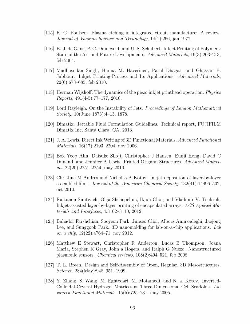
[115] R. G. Poulsen. Plasma etching in integrated circuit manufacture: A review.Journal of Vacuum Science and Technology, 14(1):266, jan 1977.
[116] B.-J. de Gans, P. C. Duineveld, and U. S. Schubert. Inkjet Printing of Polymers:State of the Art and Future Developments. Advanced Materials, 16(3):203–213,feb 2004.
[117] Madhusudan Singh, Hanna M. Haverinen, Parul Dhagat, and Ghassan E.Jabbour. Inkjet Printing-Process and Its Applications. Advanced Materials,22(6):673–685, feb 2010.
[118] HermanWijshoff. The dynamics of the piezo inkjet printhead operation. PhysicsReports, 491(4-5):77–177, 2010.
[119] Lord Rayleigh. On the Instability of Jets. Proceedings of London MathematicalSociety, 10(June 1873):4–13, 1878.
[120] Dimatix. Jettable Fluid Formulation Guidelines. Technical report, FUJIFILMDimatix Inc, Santa Clara, CA, 2013.
[121] J. A. Lewis. Direct InkWriting of 3D Functional Materials. Advanced FunctionalMaterials, 16(17):2193–2204, nov 2006.
[122] Bok Yeop Ahn, Daisuke Shoji, Christopher J Hansen, Eunji Hong, David CDunand, and Jennifer A Lewis. Printed Origami Structures. Advanced Materi-als, 22(20):2251–2254, may 2010.
[123] Christine M Andres and Nicholas A Kotov. Inkjet deposition of layer-by-layerassembled films. Journal of the American Chemical Society, 132(41):14496–502,oct 2010.
[124] Rattanon Suntivich, Olga Shchepelina, Ikjun Choi, and Vladimir V. Tsukruk.Inkjet-assisted layer-by-layer printing of encapsulated arrays. ACS Applied Ma-terials and Interfaces, 4:3102–3110, 2012.
[125] Bahador Farshchian, Sooyeon Park, Junseo Choi, Alborz Amirsadeghi, JaejongLee, and Sunggook Park. 3D nanomolding for lab-on-a-chip applications. Labon a chip, 12(22):4764–71, nov 2012.
[126] Matthew E Stewart, Christopher R Anderton, Lucas B Thompson, JoanaMaria, Stephen K Gray, John a Rogers, and Ralph G Nuzzo. Nanostructuredplasmonic sensors. Chemical reviews, 108(2):494–521, feb 2008.
[127] T. L. Breen. Design and Self-Assembly of Open, Regular, 3D Mesostructures.Science, 284(May):948–951, 1999.
[128] Y. Zhang, S. Wang, M. Eghtedari, M. Motamedi, and N. a. Kotov. Inverted-Colloidal-Crystal Hydrogel Matrices as Three-Dimensional Cell Scaffolds. Ad-vanced Functional Materials, 15(5):725–731, may 2005.
96

[129] C B Murray, C R Kagan, and M G Bawendi. Self-Organization of CdseNanocrystallites into 3-Dimensional Quantum-Dot Superlattices. Science,270(5240):1335–1338, 1995.
[130] J. W. van Honschoten, J. W. Berenschot, T. Ondarcuhu, R. G. P. Sanders,J. Sundaram, M. Elwenspoek, and N. R. Tas. Elastocapillary fabrication ofthree-dimensional microstructures. Applied Physics Letters, 97(1):014103, 2010.
[131] Jun-Hee Na, Arthur A Evans, Jinhye Bae, Maria C Chiappelli, Christian DSantangelo, Robert J Lang, Thomas C Hull, and Ryan C Hayward. Program-ming Reversibly Self-Folding Origami with Micropatterned Photo-CrosslinkablePolymer Trilayers. Advanced materials (Deerfield Beach, Fla.), pages 79–85, oct2014.
[132] Jennie Ryu, Matteo DAmato, Xiaodong Cui, Kevin N. Long, H. Jerry Qi,and Martin L. Dunn. Photo-origamiBending and folding polymers with light.Applied Physics Letters, 100(16):161908, 2012.
[133] Ying Liu, Julie K. Boyles, Jan Genzer, and Michael D. Dickey. Self-folding ofpolymer sheets using local light absorption. Soft Matter, 8(6):1764, 2012.
[134] Ren Geryak and Vladimir V Tsukruk. Reconfigurable and actuating structuresfrom soft materials. Soft matter, 10(9):1246–63, 2014.
[135] William J. Arora, Anthony J. Nichol, Henry I. Smith, and George Barbastathis.Membrane folding to achieve three-dimensional nanostructures: Nanopatternedsilicon nitride folded with stressed chromium hinges. Applied Physics Letters,88(5):053108, 2006.
[136] Noy Bassik, George M Stern, and David H Gracias. Microassembly basedon hands free origami with bidirectional curvature. Applied physics letters,95(9):91901, aug 2009.
[137] Jeong-Hyun Cho, Michael D Keung, Niels Verellen, Liesbet Lagae, Victor VMoshchalkov, Pol Van Dorpe, and David H Gracias. Nanoscale origami for 3Doptics. Small (Weinheim an der Bergstrasse, Germany), 7(14):1943–8, jul 2011.
[138] Sung Yun Yang and Michael F Rubner. Micropatterning of polymer thin filmswith pH-sensitive and cross-linkable hydrogen-bonded polyelectrolyte multilay-ers. Journal of the American Chemical Society, 124(10):2100–2101, 2002.
[139] Nicholas A. Kotov. Ordered Layered Assemblies of Nanoparticles. MRS Bul-letin, 26(12):992–997, dec 2001.
[140] Christine M Andres, Jian Zhu, Terry Shyu, Connor Flynn, and Nicholas AKotov. Shape-morphing nanocomposite origami. Langmuir : the ACS journalof surfaces and colloids, 30(19):5378–85, may 2014.
97

[141] Shaoqin Liu, Dirk G Kurth, and Dirk Volkmer. Polyoxometalates as pH-sensitive probes in self-assembled multilayers. Chemical communications (Cam-bridge, England), 10(9):976–7, may 2002.
[142] Ralf Kohler, Ingo Donch, Patrick Ott, Andre Laschewsky, Andreas Fery, andRumen Krastev. Neutron reflectometry study of swelling of polyelectrolyte mul-tilayers in water vapors: influence of charge density of the polycation. Langmuir: the ACS journal of surfaces and colloids, 25(19):11576–85, oct 2009.
[143] C Gao, E Donath, S Moya, V. Dudnik, and H. Mohwald. Elasticity of hollowpolyelectrolyte capsules prepared by the layer-by-layer technique. EuropeanPhysical Journal E, 5(1):21–27, 2001.
[144] Paul Podsiadlo, Marc Michel, Kevin Critchley, Sudhanshu Srivastava, MingQin, Jung Woo Lee, Eric Verploegen, A. John Hart, Ying Qi, and Nicholas A.Kotov. Diffusional Self-Organization in Exponential Layer-By-Layer Films withMicro- and Nanoscale Periodicity. Angewandte Chemie International Edition,48(38):7073–7077, 2009.
[145] Jian Zhu, Christine M Andres, Jiadi Xu, Ayyalusamy Ramamoorthy, ThomasTsotsis, and Nicholas a Kotov. Pseudonegative thermal expansion and the stateof water in graphene oxide layered assemblies. ACS Nano, 6(9):8357–65, oct2012.
[146] Aurelie Lafuma and David Quere. Superhydrophobic states. Nature Materials,2(7):457–60, jul 2003.
[147] Jau-ye Shiu, Chun-wen Kuo, Peilin Chen, and Chung-Yuan Mou. Fabricationof Tunable Superhydrophobic Surfaces by Nanosphere Lithography. Chemistryof Materials, 16(4):561–564, feb 2004.
[148] David Quere. Wetting and Roughness. Annual Review of Materials Research,38(1):71–99, aug 2008.
[149] Eero Huovinen, Laura Takkunen, Tarmo Korpela, Mika Suvanto, Tuula T.Pakkanen, and Tapani a. Pakkanen. Mechanically robust superhydrophobicpolymer surfaces based on protective micropillars. Langmuir, 30(5):1435–1443,2014.
[150] Lie Shen, Wenlian Qiu, Bin Liu, and Qipeng Guo. Stable superhydrophobicsurface based on silicone combustion product. RSC Adv., 4(99):56259–56262,2014.
[151] D. Oner and T. J. McCarthy. Ultra-Hydrophobic Surfaces:Effects of TopographyLength Scales on Wettability. Langmuir, 16(2):7777–7782, 2000.
[152] Kyoung G Lee, Bong Gill Choi, Byeong Il Kim, Terry Shyu, Myung Seok Oh,Sung Gap Im, Sung-Jin Chang, Tae Jae Lee, Nicholas A. Kotov, and Seok Jae
98

Lee. Scalable nanopillar arrays with layer-by-layer patterned overt and covertimages. Advanced materials (Deerfield Beach, Fla.), 26(35):6119–24, sep 2014.
[153] Alexandra Schweikart and Andreas Fery. Controlled wrinkling as a novelmethod for the fabrication of patterned surfaces. Microchimica Acta, 165(3-4):249–263, apr 2009.
[154] Sung H. Kang, Boaz Pokroy, L. Mahadevan, and Joanna Aizenberg. Controlof shape and size of nanopillar assembly by adhesion-mediated elastocapillaryinteraction. ACS Nano, 4(11):6323–6331, 2010.
[155] AK Geim, S V Dubonos, I V Grigorieva, K S Novoselov, a a Zhukov, andS Yu Shapoval. Microfabricated adhesive mimicking gecko foot-hair. Naturematerials, 2:461–463, 2003.
[156] Ren Zhu, Wengui Zhang, Chao Li, and Rusen Yang. Uniform zinc oxidenanowire arrays grown on nonepitaxial surface with general orientation con-trol. Nano letters, 13(11):5171–6, nov 2013.
[157] Y N Xia, P D Yang, Y G Sun, Y Y Wu, B Mayers, B Gates, Y D Yin, F Kim,and Y Q Yan. One-dimensional nanostructures: Synthesis, characterization,and applications. Advanced Materials, 15(5):353–389, 2003.
[158] Bernhard Wolfrum, Yulia Mourzina, Dirk Mayer, Daniel Schwaab, and AndreasOffenhausser. Fabrication of large-scale patterned gold-nanopillar arrays on asilicon substrate using imprinted porous alumina templates. Small, 2(11):1256–1260, 2006.
[159] C F Huang, Y Lin, Y K Shen, and Y M Fan. Optimal processing for hydropho-bic nanopillar polymer surfaces using nanoporous alumina template. AppliedSurface Science, 305(0):419–426, 2014.
[160] Anish Tuteja, Wonjae Choi, Minglin Ma, Joseph M Mabry, Sarah a Mazzella,Gregory C Rutledge, Gareth H McKinley, and Robert E Cohen. Designingsuperoleophobic surfaces. Science (New York, N.Y.), 318(5856):1618–22, dec2007.
[161] Sai P R Kobaku, Arun K. Kota, Duck Hyun Lee, Joseph M. Mabry, and An-ish Tuteja. Patterned superomniphobic-superomniphilic surfaces: Templatesfor site-selective self-assembly. Angewandte Chemie - International Edition,51(2):10109–10113, 2012.
[162] Tsuyoshi Sekitani, Yoshiaki Noguchi, Kenji Hata, Takanori Fukushima, TakuzoAida, and Takao Someya. A rubberlike stretchable active matrix using elasticconductors. Science (New York, N.Y.), 321(5895):1468–72, sep 2008.
[163] J Song, H Jiang, Z Liu, D Khang, Y Huang, J Rogers, C Lu, and C Koh.Buckling of a stiff thin film on a compliant substrate in large deformation.International Journal of Solids and Structures, 45(10):3107–3121, may 2008.
99

[164] Dahl-Young Khang, Jianliang Xiao, Coskun Kocabas, Scott MacLaren, TonyBanks, Hanqing Jiang, Yonggang Y Huang, and John A Rogers. Molecularscale buckling mechanics in individual aligned single-wall carbon nanotubes onelastomeric substrates. Nano letters, 8(1):124–30, jan 2008.
[165] Jonathan A Fan, Woon-Hong Yeo, Yewang Su, Yoshiaki Hattori, Woosik Lee,Sung-Young Jung, Yihui Zhang, Zhuangjian Liu, Huanyu Cheng, Leo Falgout,Mike Bajema, Todd Coleman, Dan Gregoire, Ryan J Larsen, Yonggang Huang,and John A Rogers. Fractal design concepts for stretchable electronics. Naturecommunications, 5:3266, jan 2014.
[166] M. Mirkhalaf, A. Khayer Dastjerdi, and F. Barthelat. Overcoming the brittle-ness of glass through bio-inspiration and micro-architecture. Nature communi-cations, 5:3166, jan 2014.
[167] Ahmad Khayer Dastjerdi, Reza Rabiei, and Francois Barthelat. The weakinterfaces within tough natural composites: experiments on three types of nacre.Journal of the mechanical behavior of biomedical materials, 19:50–60, mar 2013.
[168] Ying Zhang, Elisabetta a Matsumoto, Anna Peter, Pei-Chun Lin, Randall DKamien, and Shu Yang. One-Step Nanoscale Assembly of Complex Structuresvia Harnessing of an Elastic Instability. Nano letters, 8(4):1192–6, apr 2008.
[169] D. P. Holmes and A. J. Crosby. Snapping Surfaces. Advanced Materials,19(21):3589–3593, nov 2007.
[170] Srikanth Singamaneni, Katia Bertoldi, Sehoon Chang, Ji-Hyun Jang, Edwin LThomas, Mary C Boyce, and Vladimir V Tsukruk. Instabilities and patterntransformation in periodic, porous elastoplastic solid coatings. ACS appliedmaterials & interfaces, 1(1):42–7, jan 2009.
[171] Sung Hoon Kang, Sicong Shan, Wim L Noorduin, Mughees Khan, JoannaAizenberg, and Katia Bertoldi. Buckling-Induced Reversible Symmetry Break-ing and Amplification of Chirality Using Supported Cellular Structures. Ad-vanced materials (Deerfield Beach, Fla.), pages 3380–3385, may 2013.
[172] Chuan Fei Guo, Tianyi Sun, Qihan Liu, Zhigang Suo, and Zhifeng Ren. Highlystretchable and transparent nanomesh electrodes made by grain boundarylithography. Nature communications, 5:3121, 2014.
[173] Terry C. Shyu, Pablo F. Damasceno, Paul M. Dodd, Aaron Lamoureux, LizhiXu, Matthew Shlian, Max Shtein, Sharon C. Glotzer, and Nicholas A. Kotov.A kirigami approach to engineering elasticity in nanocomposites through pat-terned defects. Nature Materials, 14(August):785–790, 2015.
[174] Aaron Lamoureux, Kyusang Lee, Matthew Shlian, Stephen R. Forrest, andMax Shtein. Dynamic kirigami structures for integrated solar tracking. NatureCommunications, 6:8092, 2015.
100
[175] Bong Sup Shim, Jian Zhu, Edward Jan, Kevin Critchley, Szushen Ho, PaulPodsiadlo, Kai Sun, and Nicholas a Kotov. Multiparameter Structural Opti-mization of Single-Walled Carbon Nanotube Stiffness , and Toughness. ACSNano, 3(7):1711–1722, 2009.
[176] F.W. Peek. Dielectric Phenomena in High-Voltage Engineering. McGraw-Hill,New York, 3 edition, 1929.
[177] Yihui Zhang, Zheng Yan, Kewang Nan, Dongqing Xiao, Yuhao Liu, HaiwenLuan, Haoran Fu, XizhuWang, Qinglin Yang, JiechenWang, Wen Ren, HongzhiSi, Fei Liu, Lihen Yang, Hejun Li, Juntong Wang, Xuelin Guo, Hongying Luo,Liang Wang, Yonggang Huang, and John A. Rogers. A mechanically drivenform of Kirigami as a route to 3D mesostructures in micro/nanomembranes.Proceedings of the National Academy of Sciences, 112(38):201515602, 2015.
[178] Lewi Tonks and Irving Langmuir. Oscillations in ionized gases. Physical Review,33(2):195–210, 1929.
[179] Riccardo D’Agostino, Pietro Favia, Christian Oehr, and Michael R. Wertheimer.Low-Temperature Plasma Processing of Materials: Past, Present, and Future.Plasma Processes and Polymers, 2(1):7–15, 2005.
[180] James W Gregory, C Lon Enloe, Gabriel I Font, and Thomas E McLaughlin.Force Production Mechanism of a Dielectric-Barrier Discharge Plasma Actua-tor. Aiaa 2007-185, (January):1–13, 2007.
[181] Kunwar Pal Singh and Subrata Roy. Physics of plasma actuator operating inatmospheric air. Applied Physics Letters, 92(2008):11–13, 2008.
[182] Rasool Erfani, Hossein Zare-Behtash, Craig Hale, and Konstantinos Kontis.Development of DBD plasma actuators: The double encapsulated electrode.Acta Astronautica, 109:132–143, 2015.
[183] U. Schlickum, R. Decker, F. Klappenberger, G. Zoppellaro, S. Klyatskaya,W. Auwarter, S. Neppl, K. Kern, H. Brune, M. Ruben, and J. V. Barth. Chiralkagome lattice from simple ditopic molecular bricks. Journal of the AmericanChemical Society, 130(35):11778–11782, 2008.
[184] J. N. Grima and K. E. Evans. Auxetic behavior from rotating squares. Journalof Materials Science Letters, 19(17):1563–1565, 2000.
[185] Rivka Elbaum, Liron Zaltzman, Ingo Burgert, and Peter Fratzl. The roleof wheat awns in the seed dispersal unit. Science (New York, N.Y.),316(5826):884–6, may 2007.
[186] Matthew J Harrington, Khashayar Razghandi, Friedrich Ditsch, LorenzoGuiducci, Markus Rueggeberg, John W C Dunlop, Peter Fratzl, ChristophNeinhuis, and Ingo Burgert. Origami-like unfolding of hydro-actuated ice plantseed capsules. Nature communications, 2(May):337, jan 2011.
101

[187] John W C Dunlop, Richard Weinkamer, and Peter Fratzl. Artful interfaceswithin biological materials. Materials Today, 14(3):70–78, 2011.
[188] Srikanth Singamaneni, Katia Bertoldi, Sehoon Chang, Ji-Hyun Jang, Seth L.Young, Edwin L. Thomas, Mary C. Boyce, and Vladimir V. Tsukruk. BifurcatedMechanical Behavior of Deformed Periodic Porous Solids. Advanced FunctionalMaterials, 19(9):1426–1436, may 2009.
[189] Jongmin Shim, Claude Perdigou, Elizabeth Chen, Katia Bertoldi, and Pedro MReis. Buckling-induced encapsulation of structured elastic shells under pres-sure. Proceedings of the National Academy of Sciences of the United States ofAmerica, 109(16):5978–5983, 2012.
[190] Jatinder S. Randhawa, Kate E. Laflin, Natasha Seelam, and David H. Gracias.Microchemomechanical Systems. Advanced Functional Materials, 21(13):2395–2410, jul 2011.
[191] Yihui Zhang, Sheng Xu, Haoran Fu, Juhwan Lee, Jessica Su, Keh-Chih Hwang,John A. Rogers, and Yonggang Huang. Buckling in serpentine microstructuresand applications in elastomer-supported ultra-stretchable electronics with highareal coverage. Soft Matter, 9(33):8062, 2013.
[192] Bavani Balakrisnan, Aleksandar Nacev, Jeffrey M Burke, Abhijit Dasgupta, andElisabeth Smela. Design of compliant meanders for applications in MEMS, ac-tuators, and flexible electronics. Smart Materials and Structures, 21(7):075033,jul 2012.
[193] T. A. Schaedler, A. J. Jacobsen, A. Torrents, A. E. Sorensen, J. Lian, J. R.Greer, L. Valdevit, and W. B. Carter. Ultralight Metallic Microlattices. Science,334(6058):962–965, 2011.
[194] Xiaoyu Zheng, Howon Lee, Todd H Weisgraber, Maxim Shusteff, JoshuaDeOtte, Eric B Duoss, Joshua D Kuntz, Monika M Biener, Qi Ge, Julie aJackson, Sergei O Kucheyev, Nicholas X Fang, and Christopher M Spadac-cini. Ultralight, ultrastiff mechanical metamaterials. Science (New York, N.Y.),344(6190):1373–7, jun 2014.
[195] Lucas R Meza, Satyajit Das, and Julia R Greer. Strong, lightweight, andrecoverable three-dimensional ceramic nanolattices. Science, 345(6202):1322–1326, sep 2014.
[196] Lauren C. Montemayor, Lucas R. Meza, and Julia R. Greer. Design and fabri-cation of hollow rigid nanolattices via two-photon lithography. Advanced Engi-neering Materials, 16(2):184–189, 2014.
[197] Dongchan Jang, Lucas R Meza, Frank Greer, and Julia R Greer. Fabricationand deformation of three-dimensional hollow ceramic nanostructures. Naturematerials, 12(10):893–898, sep 2013.
102