Engineering Materials - Springer978-3-319-19758-6/1.pdf · materials and devices in accordance ......
37
Engineering Materials
Transcript of Engineering Materials - Springer978-3-319-19758-6/1.pdf · materials and devices in accordance ......

Engineering Materials

More information about this series at http://www.springer.com/series/4288

K.M. Gupta • Nishu Gupta
Advanced SemiconductingMaterials and Devices
123
K.M. GuptaDepartment of Applied MechanicsMotilal Nehru National Instituteof Technology
Allahabad, Uttar PradeshIndia
Nishu GuptaDepartment of Electronics andCommunication Engineering
Motilal Nehru National Instituteof Technology
Allahabad, Uttar PradeshIndia
ISSN 1612-1317 ISSN 1868-1212 (electronic)Engineering MaterialsISBN 978-3-319-19757-9 ISBN 978-3-319-19758-6 (eBook)DOI 10.1007/978-3-319-19758-6
Library of Congress Control Number: 2015944749
Springer Cham Heidelberg New York Dordrecht London© Springer International Publishing Switzerland 2016This work is subject to copyright. All rights are reserved by the Publisher, whether the whole or partof the material is concerned, specifically the rights of translation, reprinting, reuse of illustrations,recitation, broadcasting, reproduction on microfilms or in any other physical way, and transmissionor information storage and retrieval, electronic adaptation, computer software, or by similar or dissimilarmethodology now known or hereafter developed.The use of general descriptive names, registered names, trademarks, service marks, etc. in thispublication does not imply, even in the absence of a specific statement, that such names are exempt fromthe relevant protective laws and regulations and therefore free for general use.The publisher, the authors and the editors are safe to assume that the advice and information in thisbook are believed to be true and accurate at the date of publication. Neither the publisher nor theauthors or the editors give a warranty, express or implied, with respect to the material contained herein orfor any errors or omissions that may have been made.
Printed on acid-free paper
Springer International Publishing AG Switzerland is part of Springer Science+Business Media(www.springer.com)

Preface
This book is intended to cover the vast and fast growing field of semiconductingmaterials and devices in accordance with the modern trends. The level of the bookcovers the syllabi being taught at the undergraduate standard of engineeringinstitutes in India and abroad for students of Electronics and Telecommunication,Electrical Engineering, Materials Science, and Applied Physics. It also covers thesyllabi of various competitive and other national level examinations across theglobe. The contents of the book will be fully useful to the electronics students ofpostgraduate studies. The book may be used as a reference book by scientists,engineers, and research scholars for basic, advanced and up-to-date information.
This book is organized into six parts, containing 16 chapters. In Part I, the firsttwo Chaps. 1 and 2 provide an elementary viewpoint on properties and applicationsof semiconductor materials; some recent advances like spintronic materials, ferro-magnetic semiconductors, left-handed materials, DMS, photocatalytic semicon-ductors, etc.; materials science of crystal structures and imperfections, atomicmodels and bonding in them. Basic information on semiconductor devices, narrowand wide bandgap semiconductors are given in brief. These chapters are essentiallyneeded to develop the understanding of the subject. Chapters 3 and 4 describe thecarrier transport and excess carriers in semiconductors, respectively. These chaptersprovide detailed mathematical information about the phenomena related to varioussemiconductor behaviour.
Part II consisting of Chaps. 5 and 6, deals with junctions and interfaces. Chapter5 describes p–n junctions, diodes and their breakdown mechanism; while Chap. 6explains a large variety of specific diodes. The Part III comprises Chaps. 7–9.Chapter 7 deals with majority carrier diodes, their operation and response underdifferent biasing conditions. Chapter 8 provides information on construction,characteristics, performance and application of microwave diodes, varacter diode,photodiodes; IMPATT, TRAPATT, BARITT and Gunn diodes, etc. In Chap. 9, theoptoelectronic devices describe the solar cells, photodetectors, LEDs and semi-conductor lasers, etc.
Part IV, comprising Chaps. 10–12, deals with BJT, FETs and power semicon-ductor devices. In Chap. 10, various aspects of bipolar junction transistors are dealt
vii
in, Chap. 11 provides a thorough discussion on MESFETs, MOSFETs, IGFETs,etc. Chapter 12 focuses on p-n-p-n diode, thyristors, silicon-controlled rectifiers,bilateral devices, etc.
Part V, comprises Chaps. 13 which deals with the brief details of various aspectsof semiconductor fabrication. It elaborates the method of production of silicon,semiconductor crystal growth, zone refining, construction of microelectronic cir-cuit. It also deals with manufacturing of wafers, lithography, molecular beamepitaxy, masking, fabrication technique of p-n junction and transistor manufactur-ing processes.
The last Part VI, comprises of Chaps. 14–16. Chapter 14 incorporates special-ized semiconductors in vivid fields like solar cells, thermoelectrics, photocatalytic,plasmonics, photonic, photovoltaic semiconductors, etc. Chapters 15 and 16 pre-sents a comprehensive detail of modern trends in the research and development ofsemiconductor materials and devices. In Chap. 15, nanostructured semiconductingmaterials and devices are described; while in Chap. 16, the recent advances andemerging trends in semiconducting materials and devices are given. Both thesechapters present up-to-date information about the subject.
Basic and prerequisite information has also been included for easy transition tonewer topics. Latest developments in the fields of semiconducting materials, theirsciences, processes and applications have been accommodated. Latest topics inoptoelectronic devices, metal-semiconductor junctions, heterojunctions, MISFET,LEDs, semiconductor lasers, photodiodes, switching diodes, tunnel diodes, Gunndiode, solar cells, varactor diode, IMPATT diode, advanced semiconductors, etc.,have been included.
Topics like electron theories, high-field effects, Hall effect, transit-time effects,drift and diffusion, breakdown mechanisms, equilibrium and transient conditions,switching, biasing have been explained. A variety of semiconducting materials anddevices, microelectronics, memory devices, advance and futuristic materials aredescribed. Information on ideal diode, real diode, backward diode, etc., are pro-vided to include the contents on more advanced semiconductor devices.
Review and objective type questions based on concepts, design, construction,applications and practical orientations, are included. Wherever required, themathematical equations have been incorporated to understand the contents easilyand in-full, however, they have been kept to a minimum, throughout the text.A large number of numerical and theoretical examples have been worked-out foreaiser understanding to the readers. Numerical exercises for practice andself-valuation are also given with their answers, in order to develop confidence tousers. SI units, in general, have been incorporated throughout the text but forfamiliarity, the MKS units have also been used. Review, objective and numericalproblems are enriched with questions of different examinations of many universitiesand national level institutes. The book is substantiated by a large number of dia-grams, tables, equations and glossary of terms.
We gratefully acknowledge the authors and publishers of the books quoted inreferences which have provided guidelines in preparing this book. We also thank allthe authors and publishers of research papers published in different journals whose
viii Preface

work has been included. Every effort has been made to seek permission from thecopyright holders to reproduce the matter in this book. However, the authors of thisbook desire excuse from those contributors who could not be contacted, or fromthose whose acknowledgement is missed undeliberately.
I (K.M.Gupta, and Nishu Gupta with appropriate relations) acknowledge theinspiration and blessings of my respected mother Smt. Bela Devi, brother-in-lawSri Jawahar Lal, sister Smt. Savitri Lal, brothers Sri Gopal Das Gupta, Brij Mohan,Hari Mohan, Madan Mohan, and other family members. I am full of gratitude to mywife Rita, daughter Nidhi, son-in-law Ritesh, son Nishu, daughter-in-law Anamika,grandson Akarsh (Ram) and Ayaansh (Aditya), and granddaughter Anshika (Gauri)for the patience shown and encouragement given to complete this venture. I alsopay homage to my loving nephew Jayant (Babul) who left us for his heavenlyabode at an early age.
At this time Nishu Gupta recalls his mentor, Professor Rajeev Tripathi, andDr. Arun Prakash, Assistant Professor and Ph.D. guide for patronage and usefulguidance. I (K.M. Gupta) recall with deep sense of respect and honour my dis-tinguished early age friends (Late) Mohd. Naseem, Sri Fazlur Rahman Khan, andSri Tarak Nath Batabyal, who have always been very positive thinking humanbeings to me and to the society by their ever helping attitude. Our heartfelt thanksare due to my friends Er. K.R.D. Tewari, Chartered Civil Engineer and Consultant,Allahabad; Er. Ranjeet Singh Virmani, AGM (retd.) Punjab National Bank;my nephew Hemant Jawahar Lal (IRS), Commissioner, Income Tax, Mumbai; toSri S.C. Sant and Mr. Anurag Sant, the publishers of Umesh Publications for theircontinued support, guidance and cooperation in preparing this book. We thankMr. Vishal Kumar Gupta ‘Bishu’ for his untiring efforts in typing the variousversions of the manuscript.
The authors have attempted to contact the copyright holders of all materialreproduced in this publication and apologize to copyright holders if permission topublish in this form has not been obtained. If any copyright material has not beenacknowledged, please write and let us know so that we may rectify in future reprint.Enormous effort has been made to avoid errors and mistakes, however, theirpresence cannot be ruled out. Any suggestion to improve the standard of this book,indication towards errors, omissions and mistakes will be highly appreciated.
Allahabad, India K.M. GuptaJuly 2015 Nishu Gupta
Preface ix
Acknowledgements
The authors of this book acknowledge with heartfelt gratitude to Mr. S.C. Sant andMr. Anurag Sant, the publishers of Umesh Publications (4230/1 Ansari Road,Daryaganj, Delhi-110002) India, for being kind enough to provide substantialliterature support and valuable information that proved very useful in preparing thisbook. Authors (Dr. K.M. Gupta and Nishu Gupta) thank especially to Mr. AnuragSant for his courteous gesture.
K.M. GuptaNishu Gupta
xi
Contents
Part I Review of Fundamentals of Semiconductors
1 Semiconductor Materials: Their Properties, Applications,and Recent Advances . . . . . . . . . . . . . . . . . . . . . . . . . . . . . . . . . 31.1 Importance of Electronic and Semiconducting Materials . . . . . 31.2 Classification of Electrical and Electronic Materials,
and Status of Semiconducting Materials . . . . . . . . . . . . . . . . 41.2.1 Conductors . . . . . . . . . . . . . . . . . . . . . . . . . . . . . 51.2.2 Semiconductors . . . . . . . . . . . . . . . . . . . . . . . . . . 61.2.3 Dielectrics . . . . . . . . . . . . . . . . . . . . . . . . . . . . . 61.2.4 Superconductors . . . . . . . . . . . . . . . . . . . . . . . . . 7
1.3 Scope of Application of Semiconducting Materials . . . . . . . . 71.4 Electrons and Their Role in Semiconductivity. . . . . . . . . . . . 9
1.4.1 Valence Electrons . . . . . . . . . . . . . . . . . . . . . . . . 91.5 Classification of Materials on the Basis of Energy Gap
(or Band) . . . . . . . . . . . . . . . . . . . . . . . . . . . . . . . . . . . . 101.5.1 Valence and Conduction Band,
and Energy Gap . . . . . . . . . . . . . . . . . . . . . . . . 111.5.2 Comparison among Conductors, Semiconductors
and Insulators . . . . . . . . . . . . . . . . . . . . . . . . . . 121.6 Introduction to Semiconducting Materials. . . . . . . . . . . . . . 13
1.6.1 Different Types of Semiconducting Materials . . . . 141.6.2 Merits of Semiconducting Materials . . . . . . . . . . . 151.6.3 Characteristics of Semiconducting Materials . . . . . 151.6.4 Semiconducting Devices and Their Working
Principles . . . . . . . . . . . . . . . . . . . . . . . . . . . . . 161.7 Element Form Semiconducting Materials . . . . . . . . . . . . . . 16
1.7.1 Silicon (Si) . . . . . . . . . . . . . . . . . . . . . . . . . . . . 161.7.2 Germanium (Ge) . . . . . . . . . . . . . . . . . . . . . . . . 171.7.3 Selenium (Se) . . . . . . . . . . . . . . . . . . . . . . . . . . 171.7.4 Antimony (Sb) . . . . . . . . . . . . . . . . . . . . . . . . . 19
xiii
1.7.5 Other Elements . . . . . . . . . . . . . . . . . . . . . . . . . 191.7.6 Comparison Between Silicon and Germanium. . . . 19
1.8 Formulated (Compound and Alloyed) SemiconductorMaterials . . . . . . . . . . . . . . . . . . . . . . . . . . . . . . . . . . . . 201.8.1 Gallium Arsenide (GaAs) . . . . . . . . . . . . . . . . . . 201.8.2 Indium Antimonite (InSb). . . . . . . . . . . . . . . . . . 211.8.3 Oxides, Sulphides, Hallides, Tellurides
and Sellurides . . . . . . . . . . . . . . . . . . . . . . . . . . 221.8.4 Cadmium Sulphide (CdS) . . . . . . . . . . . . . . . . . . 221.8.5 Silicon Carbide (SiC). . . . . . . . . . . . . . . . . . . . . 231.8.6 Lead Sulphide (PbS) . . . . . . . . . . . . . . . . . . . . . 231.8.7 Indium Arsenide (InAs) . . . . . . . . . . . . . . . . . . . 23
1.9 Choicest Materials for Different Semiconductor Devices . . . 241.10 Spintronics and Spintronic Materials . . . . . . . . . . . . . . . . . 26
1.10.1 Major Fields of Spintronic Research . . . . . . . . . . 261.10.2 Operational Mechanisms of Spintronic Devices . . . 261.10.3 Working Principle of Spintronic Devices . . . . . . . 271.10.4 Emerging and Futuristic Spintronic Materials . . . . 27
1.11 Ferromagnetic Semiconductor . . . . . . . . . . . . . . . . . . . . . . 271.12 Emerging Wide Bandgap Semiconductors . . . . . . . . . . . . . 281.13 Left Handed (LH) Materials . . . . . . . . . . . . . . . . . . . . . . . 28
1.13.1 Single Negative Left-Handed Materials . . . . . . . . 291.13.2 Double Negative Left-Handed Materials . . . . . . . . 301.13.3 Negative Index Metamaterials . . . . . . . . . . . . . . . 301.13.4 Double Positive Medium . . . . . . . . . . . . . . . . . . 30
1.14 Manganese Semiconductor . . . . . . . . . . . . . . . . . . . . . . . . 311.15 Diluted Magnetic Semiconductor. . . . . . . . . . . . . . . . . . . . 311.16 Silicon: The Semiconductor Used as Raw Material
in Making ICs . . . . . . . . . . . . . . . . . . . . . . . . . . . . . . . . 321.16.1 Gallium Arsenide (GaAs) for Making
Integrated Circuit. . . . . . . . . . . . . . . . . . . . . . . . 331.17 Semiconducting Photocatalytic Materials in the Services
of Pollution Free Environment . . . . . . . . . . . . . . . . . . . . . 341.18 LED Stumps: The Advent of Semiconductors in Cricket . . . 341.19 Glimpse of Some Salient Semiconductors. . . . . . . . . . . . . . 351.20 Solved Examples . . . . . . . . . . . . . . . . . . . . . . . . . . . . . . 36Review Questions . . . . . . . . . . . . . . . . . . . . . . . . . . . . . . . . . . . . 37Objective Questions . . . . . . . . . . . . . . . . . . . . . . . . . . . . . . . . . . 38Answers . . . . . . . . . . . . . . . . . . . . . . . . . . . . . . . . . . . . . . . . . . 39References. . . . . . . . . . . . . . . . . . . . . . . . . . . . . . . . . . . . . . . . . 40
xiv Contents
2 Overview of Crystals, Bonding, Imperfections, AtomicModels, Narrow and Wide Bandgap Semiconductorsand, Semiconductor Devices . . . . . . . . . . . . . . . . . . . . . . . . . . . 412.1 Crystal Structure . . . . . . . . . . . . . . . . . . . . . . . . . . . . . . . 412.2 Bravais Crystal System . . . . . . . . . . . . . . . . . . . . . . . . . . 422.3 Miller Indices: The Crystallographic Notation
of Atomic Planes . . . . . . . . . . . . . . . . . . . . . . . . . . . . . . 432.3.1 Determining the Miller Indices
of a Given Plane . . . . . . . . . . . . . . . . . . . . . . . . 452.3.2 Family of Planes . . . . . . . . . . . . . . . . . . . . . . . . 472.3.3 Miller Indices: Crystallographic Notation
of Atomic Crystal Directions . . . . . . . . . . . . . . . 482.3.4 Family of Directions . . . . . . . . . . . . . . . . . . . . . 49
2.4 Chemical (or Atomic) Bonding . . . . . . . . . . . . . . . . . . . . . 492.4.1 Type of Bond in Semiconductors . . . . . . . . . . . . 492.4.2 Nature of Bond in Semiconductors . . . . . . . . . . . 50
2.5 Bonding Forces. . . . . . . . . . . . . . . . . . . . . . . . . . . . . . . . 502.5.1 Bonding Length and Bond Forces . . . . . . . . . . . . 51
2.6 Covalent Bond and Semiconductors. . . . . . . . . . . . . . . . . . 522.6.1 Type of Covalent Bond in Semiconductors . . . . . . 522.6.2 Bond Angle in Semiconductors . . . . . . . . . . . . . . 522.6.3 Mixed Bond in Compound Semiconductors . . . . . 53
2.7 Diamond Cubic (DC) Structure of Siliconand Germanium . . . . . . . . . . . . . . . . . . . . . . . . . . . . . . . 54
2.8 Lattice Structures of Some Compound Semiconductors . . . . 552.9 Lattice Structure of Zinc Sulphide . . . . . . . . . . . . . . . . . . . 562.10 Crystal Imperfections. . . . . . . . . . . . . . . . . . . . . . . . . . . . 56
2.10.1 Types of Imperfections. . . . . . . . . . . . . . . . . . . . 572.10.2 Point Imperfections . . . . . . . . . . . . . . . . . . . . . . 57
2.11 Bohr’s Quantum Atomic Model . . . . . . . . . . . . . . . . . . . . 582.11.1 Radii of Orbits, Velocity and Frequency
of Electrons . . . . . . . . . . . . . . . . . . . . . . . . . . . 592.11.2 Normal, Excited and Ionized Atoms . . . . . . . . . . 592.11.3 Electron Energy . . . . . . . . . . . . . . . . . . . . . . . . 602.11.4 Frequency of Radiation and Spectral Series
of Hydrogen . . . . . . . . . . . . . . . . . . . . . . . . . . . 612.12 Sommerfeld’s Relativistic Atomic Model . . . . . . . . . . . . . . 632.13 Modern Concept of Atomic Model . . . . . . . . . . . . . . . . . . 652.14 Quantum States. . . . . . . . . . . . . . . . . . . . . . . . . . . . . . . . 67
2.14.1 Pauli’s Exclusion Principle . . . . . . . . . . . . . . . . . 672.15 Important Applications of Semiconductor Devices . . . . . . . . 68
2.15.1 Brief Description of Some SemiconductorDevices . . . . . . . . . . . . . . . . . . . . . . . . . . . . . . 69
Contents xv
2.16 Narrow Bandgap Semiconductor Materials . . . . . . . . . . . . . 702.16.1 HgCdTe as Narrow Bandgap Semiconductor. . . . . 712.16.2 Applications as Infrared Detectors . . . . . . . . . . . . 722.16.3 Ternary Stannide Phase Narrow Bandgap
Semiconductors: Na2MgSn . . . . . . . . . . . . . . . . . 722.17 Wide Bandgap Semiconductor . . . . . . . . . . . . . . . . . . . . . 74
2.17.1 Advances in Wide Bandgap Materialsfor Semiconductor Spintronics. . . . . . . . . . . . . . . 74
2.17.2 Future Aspect of Wide Bandgap MaterialsPower Generating Window . . . . . . . . . . . . . . . . . 75
2.17.3 Recent Advances in Wide Bandgap Materials . . . . 762.18 Rectifiers . . . . . . . . . . . . . . . . . . . . . . . . . . . . . . . . . . . . 76
2.18.1 Selenium Rectifier . . . . . . . . . . . . . . . . . . . . . . . 762.19 Solved Examples . . . . . . . . . . . . . . . . . . . . . . . . . . . . . . 77Review Questions . . . . . . . . . . . . . . . . . . . . . . . . . . . . . . . . . . . . 79Numerical Problems . . . . . . . . . . . . . . . . . . . . . . . . . . . . . . . . . . 81Objective Questions . . . . . . . . . . . . . . . . . . . . . . . . . . . . . . . . . . 83Answers . . . . . . . . . . . . . . . . . . . . . . . . . . . . . . . . . . . . . . . . . . 85References. . . . . . . . . . . . . . . . . . . . . . . . . . . . . . . . . . . . . . . . . 85
3 Carrier Transport in Semiconductors . . . . . . . . . . . . . . . . . . . . 873.1 Electrons and Their Role in Conductivity . . . . . . . . . . . . . . 87
3.1.1 Valence Electrons . . . . . . . . . . . . . . . . . . . . . . . 883.1.2 Free Electrons . . . . . . . . . . . . . . . . . . . . . . . . . . 88
3.2 Electron Theories of Solids . . . . . . . . . . . . . . . . . . . . . . . 883.2.1 Free Electron Theory . . . . . . . . . . . . . . . . . . . . . 893.2.2 Mechanism of Conduction by Free Electrons . . . . 90
3.3 Energy Band Theory . . . . . . . . . . . . . . . . . . . . . . . . . . . . 913.4 Brillouin Zone Theory . . . . . . . . . . . . . . . . . . . . . . . . . . . 93
3.4.1 Meaning of Brillouin Zones . . . . . . . . . . . . . . . . 943.4.2 First and Second Brillouin Zones . . . . . . . . . . . . 953.4.3 Brillouin Zones for Simple Cubic Lattice . . . . . . . 963.4.4 Brillouin Zones for BCC, FCC
and HCP Lattices . . . . . . . . . . . . . . . . . . . . . . . 973.5 Direct and Indirect Energy Band Semiconductors . . . . . . . . 98
3.5.1 Differences Between Direct and IndirectSemiconductors . . . . . . . . . . . . . . . . . . . . . . . . . 99
3.5.2 Variation of Eg with Alloy Composition. . . . . . . . 1003.5.3 Effect of Alloying on GaAs1–xPx . . . . . . . . . . . . . 1003.5.4 Charge Carriers in Semiconductors . . . . . . . . . . . 1023.5.5 Fermi Energy Level . . . . . . . . . . . . . . . . . . . . . . 1023.5.6 Fermi-Dirac Probability Distribution . . . . . . . . . . 103
3.6 Intrinsic Semiconductors . . . . . . . . . . . . . . . . . . . . . . . . . 1043.6.1 Energy Diagram . . . . . . . . . . . . . . . . . . . . . . . . 1053.6.2 Holes, Mobility and Conductivity . . . . . . . . . . . . 106
xvi Contents

3.7 Extrinsic Semiconductors . . . . . . . . . . . . . . . . . . . . . . . . . 1083.7.1 n-Type Semiconductors and Their
Energy Diagram . . . . . . . . . . . . . . . . . . . . . . . . 1083.7.2 p-Type Semiconductors and Their
Energy Diagram . . . . . . . . . . . . . . . . . . . . . . . . 1093.8 Effective Mass . . . . . . . . . . . . . . . . . . . . . . . . . . . . . . . . 1123.9 Carrier Concentrations . . . . . . . . . . . . . . . . . . . . . . . . . . . 112
3.9.1 Density of State, and Electron and HoleConcentration at Equilibrium . . . . . . . . . . . . . . . 113
3.10 Temperature Dependency of Carrier Concentrations. . . . . . . 1163.10.1 Temperature Dependency of ni . . . . . . . . . . . . . . 117
3.11 Drift of Carriers in Electric and Magnetic Fields . . . . . . . . . 1183.11.1 Drift Velocity and Collision Time . . . . . . . . . . . . 1183.11.2 Mean Free Path (or Mean Free Length)
and Conductivity . . . . . . . . . . . . . . . . . . . . . . . . 1213.12 Effects of Temperature on Mobility of Carriers . . . . . . . . . . 121
3.12.1 Effects of Doping on Mobility . . . . . . . . . . . . . . 1223.13 Degenerate Semiconductors . . . . . . . . . . . . . . . . . . . . . . . 123
3.13.1 Effect of Heavy Doping . . . . . . . . . . . . . . . . . . . 1233.13.2 Degenerate Types . . . . . . . . . . . . . . . . . . . . . . . 1243.13.3 Filled and Empty Energy States in Conventional
and Degenerate Semiconductors . . . . . . . . . . . . . 1243.14 High-Field Effects . . . . . . . . . . . . . . . . . . . . . . . . . . . . . . 1263.15 The Hall Effect . . . . . . . . . . . . . . . . . . . . . . . . . . . . . . . . 126
3.15.1 Significance of Hall Effect . . . . . . . . . . . . . . . . . 1273.16 Relation Between Density of States and Fermi Energy. . . . . 131
3.16.1 Quantization of Energyi.e. 3-dimensionalization . . . . . . . . . . . . . . . . . . . 132
3.16.2 Momentum Space . . . . . . . . . . . . . . . . . . . . . . . 1323.16.3 Fermi Sphere . . . . . . . . . . . . . . . . . . . . . . . . . . 1323.16.4 Derivation of Different Fermi Parameters . . . . . . . 1333.16.5 Relation Among Density of Fermi States
(EF), EF and N . . . . . . . . . . . . . . . . . . . . . . . . . 1343.17 Solved Examples . . . . . . . . . . . . . . . . . . . . . . . . . . . . . . 137Review Questions . . . . . . . . . . . . . . . . . . . . . . . . . . . . . . . . . . . . 140Numerical Problems . . . . . . . . . . . . . . . . . . . . . . . . . . . . . . . . . . 141Objective Type Questions . . . . . . . . . . . . . . . . . . . . . . . . . . . . . . 142Answers . . . . . . . . . . . . . . . . . . . . . . . . . . . . . . . . . . . . . . . . . . 143Reference . . . . . . . . . . . . . . . . . . . . . . . . . . . . . . . . . . . . . . . . . 144
4 Excess Carriers in Semiconductors . . . . . . . . . . . . . . . . . . . . . . 1454.1 Introduction . . . . . . . . . . . . . . . . . . . . . . . . . . . . . . . . . . 1454.2 Optical Absorption . . . . . . . . . . . . . . . . . . . . . . . . . . . . . 146
4.2.1 Mechanism . . . . . . . . . . . . . . . . . . . . . . . . . . . . 1474.2.2 Absorption Coefficient . . . . . . . . . . . . . . . . . . . . 147
Contents xvii
4.2.3 Factors Affecting the Absorption Coefficient. . . . . 1494.2.4 Capability of a Material to Absorb Light . . . . . . . 152
4.3 Luminescence . . . . . . . . . . . . . . . . . . . . . . . . . . . . . . . . . 1524.3.1 Photo-Luminescence . . . . . . . . . . . . . . . . . . . . . 153
4.4 Phosphorescence . . . . . . . . . . . . . . . . . . . . . . . . . . . . . . . 1534.4.1 Phosphorescence Materials . . . . . . . . . . . . . . . . . 1544.4.2 Mechanism of Excitation and Recombination
in Photo-Luminescence . . . . . . . . . . . . . . . . . . . 1544.5 Electro-Luminescence . . . . . . . . . . . . . . . . . . . . . . . . . . . 155
4.5.1 Examples of Electroluminescent Materials . . . . . . 1564.5.2 Practical Implementations . . . . . . . . . . . . . . . . . . 1564.5.3 Advantageous Features. . . . . . . . . . . . . . . . . . . . 157
4.6 Carrier Lifetime . . . . . . . . . . . . . . . . . . . . . . . . . . . . . . . 1584.7 Derivation of Carrier Lifetime in Direct Recombination
Mechanism. . . . . . . . . . . . . . . . . . . . . . . . . . . . . . . . . . . 1584.7.1 Assumptions and Simplifications . . . . . . . . . . . . . 1594.7.2 Solution of Equation to Determine Lifetime . . . . . 1604.7.3 Generalization of Expression. . . . . . . . . . . . . . . . 160
4.8 Indirect Recombination (i.e. Capture or TrappingProcess) . . . . . . . . . . . . . . . . . . . . . . . . . . . . . . . . . . . . . 161
4.9 Steady State Carrier Generation . . . . . . . . . . . . . . . . . . . . 1624.9.1 Quasi-Fermi Levels . . . . . . . . . . . . . . . . . . . . . . 163
4.10 Photoconductivity . . . . . . . . . . . . . . . . . . . . . . . . . . . . . . 1644.10.1 Applications of Photoconductive Devices . . . . . . . 1644.10.2 Photoconductive Materials and Factors Affecting
Their Selection . . . . . . . . . . . . . . . . . . . . . . . . . 1654.10.3 Factors Affecting the Selection
of Semiconductor . . . . . . . . . . . . . . . . . . . . . . . 1664.11 Photoconductive Cell . . . . . . . . . . . . . . . . . . . . . . . . . . . . 167
4.11.1 Photo-Multiplier Tube . . . . . . . . . . . . . . . . . . . . 1674.12 Diffusion of Carriers . . . . . . . . . . . . . . . . . . . . . . . . . . . . 168
4.12.1 Determining the Rate of Electronand Hole Diffusion . . . . . . . . . . . . . . . . . . . . . . 169
4.12.2 Analysis of Drift and Diffusion Carriers . . . . . . . . 1714.13 Einstein Relation. . . . . . . . . . . . . . . . . . . . . . . . . . . . . . . 1724.14 Continuity Equation (i.e. Diffusion and Recombination). . . . 173
4.14.1 Diffusion Equation and Diffusion Length . . . . . . . 1744.15 Transport of Charges and Impurity Distribution Profile
During Diffusion. . . . . . . . . . . . . . . . . . . . . . . . . . . . . . . 1754.15.1 Solution by Error Function Method . . . . . . . . . . . 1754.15.2 Complementary Error Function and Gaussian
Distribution . . . . . . . . . . . . . . . . . . . . . . . . . . . 176
xviii Contents

4.16 Long Diode and Short Diode . . . . . . . . . . . . . . . . . . . . . . 1794.16.1 Voltage-Variable Capacitance . . . . . . . . . . . . . . . 1804.16.2 Effect of Dielectric Constant on Width of the
Transition Region and Voltage Capacitance . . . . . 1804.17 Solved Examples . . . . . . . . . . . . . . . . . . . . . . . . . . . . . . 181Review Questions . . . . . . . . . . . . . . . . . . . . . . . . . . . . . . . . . . . . 186Numerical Problems . . . . . . . . . . . . . . . . . . . . . . . . . . . . . . . . . . 187Objective Questions . . . . . . . . . . . . . . . . . . . . . . . . . . . . . . . . . . 188Answers . . . . . . . . . . . . . . . . . . . . . . . . . . . . . . . . . . . . . . . . . . 189References. . . . . . . . . . . . . . . . . . . . . . . . . . . . . . . . . . . . . . . . . 189
Part II Junction and Interfaces
5 P-N Junctions and Their Breakdown Mechanisms . . . . . . . . . . . 1935.1 Junction Diode . . . . . . . . . . . . . . . . . . . . . . . . . . . . . . . . 193
5.1.1 P-N Diode (or P-N Junction Diode) . . . . . . . . . . . 1945.1.2 Applications of P-N Diode . . . . . . . . . . . . . . . . . 194
5.2 Equilibrium Conditions . . . . . . . . . . . . . . . . . . . . . . . . . . 1955.2.1 Electrostatic (or Contact) Potential . . . . . . . . . . . . 1955.2.2 Establishing the Relation Between Contact
Potential and Doping Concentrations . . . . . . . . . . 1975.3 Fermi Level at Equilibrium . . . . . . . . . . . . . . . . . . . . . . . 199
5.3.1 Space Charge at Junction . . . . . . . . . . . . . . . . . . 2015.3.2 Determining the Maximum Value
of Electric Field . . . . . . . . . . . . . . . . . . . . . . . . 2025.4 Determining the Width of Depletion Region
and Penetration Depth . . . . . . . . . . . . . . . . . . . . . . . . . . . 2035.4.1 Determining the Penetration Depth
in Depletion Region. . . . . . . . . . . . . . . . . . . . . . 2045.5 Biased Junctions . . . . . . . . . . . . . . . . . . . . . . . . . . . . . . . 2065.6 Working of p-n Diode When not Connected to a Battery . . . 208
5.6.1 Diffusion of Holes and Electrons. . . . . . . . . . . . . 2085.6.2 Set-Up of Barrier. . . . . . . . . . . . . . . . . . . . . . . . 2085.6.3 Formation of Depletion (or Space Charge)
Region . . . . . . . . . . . . . . . . . . . . . . . . . . . . . . . 2085.6.4 Flow of Drift and Diffusion Current . . . . . . . . . . 209
5.7 Forward Biased p-n Junction . . . . . . . . . . . . . . . . . . . . . . 2095.7.1 Voltage-Current Characteristics . . . . . . . . . . . . . . 2105.7.2 Voltage-Ampere Equation and Its Temperature
Dependence . . . . . . . . . . . . . . . . . . . . . . . . . . . 2105.8 Reverse Biased P-N Junction . . . . . . . . . . . . . . . . . . . . . . 211
5.8.1 Reverse-Bias Characteristics of a p-n Diode . . . . . 2125.8.2 Reverse Saturation Current . . . . . . . . . . . . . . . . . 213
Contents xix
5.9 Comparison of the Effects of No-bias, Forward-Biasand Reverse-Bias at a P-N Junction. . . . . . . . . . . . . . . . . . 2145.9.1 Diode Equation . . . . . . . . . . . . . . . . . . . . . . . . . 2145.9.2 Poisson’s Equation . . . . . . . . . . . . . . . . . . . . . . 215
5.10 Volt-Ampere Characteristics . . . . . . . . . . . . . . . . . . . . . . . 2155.10.1 In Forward Biasing . . . . . . . . . . . . . . . . . . . . . . 2155.10.2 In Reverse Biasing . . . . . . . . . . . . . . . . . . . . . . 216
5.11 Junction Breakdown Mechanisms . . . . . . . . . . . . . . . . . . . 2175.11.1 Zener Breakdown . . . . . . . . . . . . . . . . . . . . . . . 2175.11.2 Avalanche Breakdown . . . . . . . . . . . . . . . . . . . . 218
5.12 Junction Capacitance . . . . . . . . . . . . . . . . . . . . . . . . . . . . 2195.13 Rectifying Diodes . . . . . . . . . . . . . . . . . . . . . . . . . . . . . . 219
5.13.1 Half-Wave Rectifier . . . . . . . . . . . . . . . . . . . . . . 2205.13.2 Full-Wave Rectifier . . . . . . . . . . . . . . . . . . . . . . 221
5.14 Zener Diode . . . . . . . . . . . . . . . . . . . . . . . . . . . . . . . . . . 2225.14.1 Zener Diode for Meter Protection . . . . . . . . . . . . 2225.14.2 Zener Diode as Peak Clipper . . . . . . . . . . . . . . . 223
5.15 The Breakdown Diode . . . . . . . . . . . . . . . . . . . . . . . . . . . 2245.15.1 Use of Diodes in DC Power Supplies . . . . . . . . . 224
5.16 Solved Examples . . . . . . . . . . . . . . . . . . . . . . . . . . . . . . 225Review Questions . . . . . . . . . . . . . . . . . . . . . . . . . . . . . . . . . . . . 229Numerical Problems . . . . . . . . . . . . . . . . . . . . . . . . . . . . . . . . . . 231Objective Questions . . . . . . . . . . . . . . . . . . . . . . . . . . . . . . . . . . 231Answers . . . . . . . . . . . . . . . . . . . . . . . . . . . . . . . . . . . . . . . . . . 234Reference . . . . . . . . . . . . . . . . . . . . . . . . . . . . . . . . . . . . . . . . . 234
6 Different Types of Diodes, Ideal and Real Diodes,Switching Diodes, Abrupt and Graded Junctions . . . . . . . . . . . . 2356.1 Examples of Diodes . . . . . . . . . . . . . . . . . . . . . . . . . . . . 235
6.1.1 Zener Diodes . . . . . . . . . . . . . . . . . . . . . . . . . . 2366.1.2 Avalanche Diodes . . . . . . . . . . . . . . . . . . . . . . . 2366.1.3 Cat’s Whisker (or Crystal) Diodes . . . . . . . . . . . . 2366.1.4 Thermal Diodes. . . . . . . . . . . . . . . . . . . . . . . . . 2376.1.5 Constant Current Diodes . . . . . . . . . . . . . . . . . . 2376.1.6 Photodiodes . . . . . . . . . . . . . . . . . . . . . . . . . . . 2376.1.7 PIN Diodes. . . . . . . . . . . . . . . . . . . . . . . . . . . . 2376.1.8 Schottky Diodes . . . . . . . . . . . . . . . . . . . . . . . . 2386.1.9 Gold-Doped Diodes . . . . . . . . . . . . . . . . . . . . . . 2386.1.10 Super Barrier Diodes . . . . . . . . . . . . . . . . . . . . . 2386.1.11 Varicap (or Varactor) Diodes . . . . . . . . . . . . . . . 2386.1.12 Gunn Diodes . . . . . . . . . . . . . . . . . . . . . . . . . . 2396.1.13 Esaki (or Tunnel) Diodes . . . . . . . . . . . . . . . . . . 2396.1.14 Light-Emitting Diodes (LEDs) . . . . . . . . . . . . . . 2396.1.15 Laser Diodes. . . . . . . . . . . . . . . . . . . . . . . . . . . 239
xx Contents
6.1.16 Transient Voltage Suppression (TVS) Diode . . . . . 2406.1.17 Snap-Off (or Step Recovery) Diodes (SRD) . . . . . 240
6.2 Symbolic Representation of Different Diodes . . . . . . . . . . . 2406.3 The Diode Model . . . . . . . . . . . . . . . . . . . . . . . . . . . . . . 2416.4 Real Diodes . . . . . . . . . . . . . . . . . . . . . . . . . . . . . . . . . . 242
6.4.1 Ideal Diode Versus Real Diode . . . . . . . . . . . . . . 2436.5 Different Conditions of the Working of P-N Junctions . . . . . 2446.6 Transient Conditions . . . . . . . . . . . . . . . . . . . . . . . . . . . . 2446.7 Time Dependent Variation in Space Charge . . . . . . . . . . . . 245
6.7.1 Determining the Solution for Stored Charge . . . . . 2466.8 Reverse Recovery Transient . . . . . . . . . . . . . . . . . . . . . . . 2476.9 Switching Diodes . . . . . . . . . . . . . . . . . . . . . . . . . . . . . . 248
6.9.1 Improving the Switching Speed. . . . . . . . . . . . . . 2486.9.2 Narrow Base Diode . . . . . . . . . . . . . . . . . . . . . . 249
6.10 Capacitance of P-N Junctions . . . . . . . . . . . . . . . . . . . . . . 2496.10.1 Derivation of the Expression
for Junction Capacitance . . . . . . . . . . . . . . . . . . 2506.11 Linearly Graded, Abrupt and Hyperabrupt Junctions . . . . . . 251
6.11.1 Doping Profile . . . . . . . . . . . . . . . . . . . . . . . . . 2526.12 Graded Junctions . . . . . . . . . . . . . . . . . . . . . . . . . . . . . . 2536.13 Solved Examples . . . . . . . . . . . . . . . . . . . . . . . . . . . . . . 255Review Questions . . . . . . . . . . . . . . . . . . . . . . . . . . . . . . . . . . . . 257Objective Questions . . . . . . . . . . . . . . . . . . . . . . . . . . . . . . . . . . 258Answers . . . . . . . . . . . . . . . . . . . . . . . . . . . . . . . . . . . . . . . . . . 259Reference . . . . . . . . . . . . . . . . . . . . . . . . . . . . . . . . . . . . . . . . . 259
Part III Majority Carrier Diodes, Microwave Diodes,and Optoelectronic Devices
7 Majority Carrier Diodes (Tunnel Diode, Backward Diode,Schottky Barrier Diode, Ohmic Contacts,and Heterojunctions). . . . . . . . . . . . . . . . . . . . . . . . . . . . . . . . . 2637.1 Introduction to Microwave Devices . . . . . . . . . . . . . . . . . . 2637.2 Tunnel Diodes . . . . . . . . . . . . . . . . . . . . . . . . . . . . . . . . 2647.3 Tunnel Diode Operation. . . . . . . . . . . . . . . . . . . . . . . . . . 265
7.3.1 Equilibrium or Zero-Bias Condition . . . . . . . . . . . 2657.3.2 Small Reverse Bias Condition . . . . . . . . . . . . . . . 2667.3.3 Small Forward Bias Condition . . . . . . . . . . . . . . 2667.3.4 Increased Forward Bias Condition . . . . . . . . . . . . 267
7.4 Response of a Tunnel Diode Beyond the NegativeResistance Region . . . . . . . . . . . . . . . . . . . . . . . . . . . . . . 267
7.5 Total Tunnel Diode Characteristic . . . . . . . . . . . . . . . . . . . 268
Contents xxi

7.6 Transit Time Device . . . . . . . . . . . . . . . . . . . . . . . . . . . . 2697.6.1 Transit Time Effects . . . . . . . . . . . . . . . . . . . . . 2697.6.2 Requirements of a Good Transit Time Device. . . . 269
7.7 The Backward Diode. . . . . . . . . . . . . . . . . . . . . . . . . . . . 2707.7.1 I-V Characteristics of Backward Diode. . . . . . . . . 2707.7.2 Applications of Backward Diode . . . . . . . . . . . . . 271
7.8 Metal-Semiconductor Junctions . . . . . . . . . . . . . . . . . . . . . 2717.9 Schottky Diodes . . . . . . . . . . . . . . . . . . . . . . . . . . . . . . . 271
7.9.1 Case I: Mechanism of Schottky DiodeWhen the Semiconductor Is of n-Type . . . . . . . . . 272
7.9.2 Case II: Mechanism of Schottky DiodeWhen the Semiconductor Is of p-Type . . . . . . . . . 273
7.9.3 Limitations of Schottky Barrier Junctions . . . . . . . 2737.9.4 Characteristics of Schottky Diode . . . . . . . . . . . . 2747.9.5 Applications . . . . . . . . . . . . . . . . . . . . . . . . . . . 276
7.10 Ohmic Contacts . . . . . . . . . . . . . . . . . . . . . . . . . . . . . . . 2777.11 Heterojunctions. . . . . . . . . . . . . . . . . . . . . . . . . . . . . . . . 277
7.11.1 Unique Behaviour of Heterojunctions. . . . . . . . . . 2787.11.2 Band Discontinuities and Band Bending. . . . . . . . 279
7.12 Potential Well in Heterojunction . . . . . . . . . . . . . . . . . . . . 281Review Questions . . . . . . . . . . . . . . . . . . . . . . . . . . . . . . . . . . . . 282
8 Microwave Diodes (Varactor Diode, p-i-n Diode,IMPATT Diode, TRAPATT Diode, BARITT Diode, etc.) . . . . . . 2858.1 Varactor Diode . . . . . . . . . . . . . . . . . . . . . . . . . . . . . . . . 285
8.1.1 V–I Characteristics of Varactor Diode . . . . . . . . . 2868.1.2 Performance Characteristics of Varactor Diode . . . 2878.1.3 Applications of Varactor Diodes . . . . . . . . . . . . . 289
8.2 Photodiodes . . . . . . . . . . . . . . . . . . . . . . . . . . . . . . . . . . 2898.2.1 Basic Construction of a Photodiode . . . . . . . . . . . 2908.2.2 p-n Photodiode . . . . . . . . . . . . . . . . . . . . . . . . . 2918.2.3 p-i-n Photodiode . . . . . . . . . . . . . . . . . . . . . . . . 2928.2.4 Avalanche Photodiode . . . . . . . . . . . . . . . . . . . . 2938.2.5 Mid-Infrared Photodiodes . . . . . . . . . . . . . . . . . . 295
8.3 The IMPATT Diode . . . . . . . . . . . . . . . . . . . . . . . . . . . . 2958.3.1 Operational Mechanism . . . . . . . . . . . . . . . . . . . 296
8.4 Trapatt Diode . . . . . . . . . . . . . . . . . . . . . . . . . . . . . . . . . 2968.4.1 Plasma Formation in TRAPATT Diode . . . . . . . . 2978.4.2 Operation . . . . . . . . . . . . . . . . . . . . . . . . . . . . . 2978.4.3 Advantages. . . . . . . . . . . . . . . . . . . . . . . . . . . . 2988.4.4 Applications of TRAPATT Devices . . . . . . . . . . . 298
8.5 BARITT Diode. . . . . . . . . . . . . . . . . . . . . . . . . . . . . . . . 2988.5.1 Structure of BARITT Diode . . . . . . . . . . . . . . . . 2988.5.2 Performance of BARITT Diode. . . . . . . . . . . . . . 299
xxii Contents

8.6 Transferred Electron Mechanism . . . . . . . . . . . . . . . . . . . . 2998.6.1 Valleys in Conduction Band . . . . . . . . . . . . . . . . 2998.6.2 Negative Differential Conductivity. . . . . . . . . . . . 3008.6.3 Dependence of Electron Velocity
on Electric Field . . . . . . . . . . . . . . . . . . . . . . . . 3008.7 The Gunn Diode . . . . . . . . . . . . . . . . . . . . . . . . . . . . . . . 301
8.7.1 Materials and Fabrication . . . . . . . . . . . . . . . . . . 3028.7.2 Dielectric Relaxation Time in Respect
of the Gunn Diode . . . . . . . . . . . . . . . . . . . . . . 3038.7.3 Dependence of Electron Drift Velocity
on Electric Field for a Gunn Diode . . . . . . . . . . . 3038.8 Dovett Diode . . . . . . . . . . . . . . . . . . . . . . . . . . . . . . . . . 3048.9 Solved Examples . . . . . . . . . . . . . . . . . . . . . . . . . . . . . . 304Review Questions . . . . . . . . . . . . . . . . . . . . . . . . . . . . . . . . . . . . 306Objective Questions . . . . . . . . . . . . . . . . . . . . . . . . . . . . . . . . . . 307Answers . . . . . . . . . . . . . . . . . . . . . . . . . . . . . . . . . . . . . . . . . . 309
9 Optoelectronic Devices . . . . . . . . . . . . . . . . . . . . . . . . . . . . . . . 3119.1 Introduction to Optoelectronic Devices. . . . . . . . . . . . . . . . 311
9.1.1 Salient Applications . . . . . . . . . . . . . . . . . . . . . . 3129.1.2 Optoelectronic Semiconductor Devices . . . . . . . . . 313
9.2 Optical Properties . . . . . . . . . . . . . . . . . . . . . . . . . . . . . . 3159.2.1 Current and Voltage Characteristics
of an Illuminated Junction . . . . . . . . . . . . . . . . . 3159.3 Solar Cells . . . . . . . . . . . . . . . . . . . . . . . . . . . . . . . . . . . 317
9.3.1 Working Principle . . . . . . . . . . . . . . . . . . . . . . . 3179.3.2 Construction and Working . . . . . . . . . . . . . . . . . 317
9.4 Factors Affecting the Efficiency of Solar Cells . . . . . . . . . . 3199.4.1 Effect of Energy Gaps . . . . . . . . . . . . . . . . . . . . 3199.4.2 Effect of Absorber . . . . . . . . . . . . . . . . . . . . . . . 3199.4.3 Effect of Diffusion Length . . . . . . . . . . . . . . . . . 320
9.5 Solar Cell Fabrication and Materials . . . . . . . . . . . . . . . . . 3209.5.1 Advantages and Limitations of Solar Cells . . . . . . 3219.5.2 Applications of Solar Cells . . . . . . . . . . . . . . . . . 3219.5.3 Importance of Fill Factor in Design
of Solar Cell . . . . . . . . . . . . . . . . . . . . . . . . . . . 3229.6 Photodetectors . . . . . . . . . . . . . . . . . . . . . . . . . . . . . . . . 322
9.6.1 Working Principle . . . . . . . . . . . . . . . . . . . . . . . 3239.6.2 Requirements of a Good Photodetector. . . . . . . . . 3249.6.3 Method to Achieve a Fast Responding Speed . . . . 324
9.7 Different Types of Photodetectors . . . . . . . . . . . . . . . . . . . 3259.7.1 Construction of a p-i-n Photodetector . . . . . . . . . . 3259.7.2 Construction of a Silicon Heterointerface
Photodetector (SHIP) . . . . . . . . . . . . . . . . . . . . . 326
Contents xxiii

9.7.3 Photoconductive Detector . . . . . . . . . . . . . . . . . . 3269.7.4 Choice of Materials for Photodetectors . . . . . . . . . 328
9.8 Light Emitting Diodes . . . . . . . . . . . . . . . . . . . . . . . . . . . 3289.8.1 Construction and Working of LED . . . . . . . . . . . 3289.8.2 Construction of a LED for Fibre-Optic System . . . 3299.8.3 Advantages, Applications and Specifications
of LEDs . . . . . . . . . . . . . . . . . . . . . . . . . . . . . . 3309.8.4 Light Emitting Materials. . . . . . . . . . . . . . . . . . . 3309.8.5 A New Generation LED: Gallium Nitride
Based Light Emitting Diodes . . . . . . . . . . . . . . . 3329.9 Semiconductor Lasers . . . . . . . . . . . . . . . . . . . . . . . . . . . 333
9.9.1 Classification of Lasers . . . . . . . . . . . . . . . . . . . 3339.9.2 Merits of Semiconductor Lasers . . . . . . . . . . . . . 3349.9.3 Characteristics and Working . . . . . . . . . . . . . . . . 3349.9.4 Properties of Laser Light . . . . . . . . . . . . . . . . . . 3359.9.5 Laser Applications. . . . . . . . . . . . . . . . . . . . . . . 3369.9.6 Materials for Semiconductor Lasers . . . . . . . . . . . 3379.9.7 Homojunction Laser and Hetero-Junction Laser. . . 338
9.10 Laser Diode . . . . . . . . . . . . . . . . . . . . . . . . . . . . . . . . . . 3389.11 Light Dependent Resistors (LDRs) . . . . . . . . . . . . . . . . . . 3399.12 Overlight Detector. . . . . . . . . . . . . . . . . . . . . . . . . . . . . . 3409.13 Phototransistor . . . . . . . . . . . . . . . . . . . . . . . . . . . . . . . . 341
9.13.1 Differences between Phototransistorand Photodiode . . . . . . . . . . . . . . . . . . . . . . . . . 341
9.14 Solved Examples . . . . . . . . . . . . . . . . . . . . . . . . . . . . . . 343Review Questions . . . . . . . . . . . . . . . . . . . . . . . . . . . . . . . . . . . . 347Objective Questions . . . . . . . . . . . . . . . . . . . . . . . . . . . . . . . . . . 348Answers . . . . . . . . . . . . . . . . . . . . . . . . . . . . . . . . . . . . . . . . . . 350References. . . . . . . . . . . . . . . . . . . . . . . . . . . . . . . . . . . . . . . . . 350
Part IV BJT and FET Transistors, and Power Devices
10 Bipolar Junction Transistors . . . . . . . . . . . . . . . . . . . . . . . . . . . 35310.1 Introduction . . . . . . . . . . . . . . . . . . . . . . . . . . . . . . . . . . 353
10.1.1 Types of Transistors . . . . . . . . . . . . . . . . . . . . . 35410.2 Bipolar Junction Transistor (BJT) . . . . . . . . . . . . . . . . . . . 354
10.2.1 Construction of BJT . . . . . . . . . . . . . . . . . . . . . 35410.3 Fundamentals of BJT Operation . . . . . . . . . . . . . . . . . . . . 357
10.3.1 Transistor Biasing . . . . . . . . . . . . . . . . . . . . . . . 35910.3.2 Transistor Currents . . . . . . . . . . . . . . . . . . . . . . 360
10.4 Transistor Circuit Configurationsand Their Characteristics . . . . . . . . . . . . . . . . . . . . . . . . . 36110.4.1 Common-Base (CB) Characteristics . . . . . . . . . . . 36210.4.2 Common-Emitter (CE) Configuration . . . . . . . . . . 366
xxiv Contents
10.5 Comparison Between CB, CE and CC Configurations . . . . . 37010.6 Amplification with BJTs . . . . . . . . . . . . . . . . . . . . . . . . . 370
10.6.1 Amplification with CB Configuration. . . . . . . . . . 37110.6.2 Amplification with CE Configuration . . . . . . . . . . 37210.6.3 Amplification with CC Configuration. . . . . . . . . . 37310.6.4 Phase Reversal in Amplifiers . . . . . . . . . . . . . . . 374
10.7 BJT Fabrication . . . . . . . . . . . . . . . . . . . . . . . . . . . . . . . 37510.7.1 Diffused Junction Transistors . . . . . . . . . . . . . . . 375
10.8 Solved Examples . . . . . . . . . . . . . . . . . . . . . . . . . . . . . . 375Review Questions . . . . . . . . . . . . . . . . . . . . . . . . . . . . . . . . . . . . 379Numerical Problems . . . . . . . . . . . . . . . . . . . . . . . . . . . . . . . . . . 380Objective Questions . . . . . . . . . . . . . . . . . . . . . . . . . . . . . . . . . . 382Answers . . . . . . . . . . . . . . . . . . . . . . . . . . . . . . . . . . . . . . . . . . 383Reference . . . . . . . . . . . . . . . . . . . . . . . . . . . . . . . . . . . . . . . . . 383
11 Metal Semiconductor Field Effect Transistors, MOS Transistors,and Charge Coupled Device . . . . . . . . . . . . . . . . . . . . . . . . . . . 38511.1 Introduction . . . . . . . . . . . . . . . . . . . . . . . . . . . . . . . . . . 38511.2 Field-Effect Transistor (FET) . . . . . . . . . . . . . . . . . . . . . . 386
11.2.1 Applications of FETs . . . . . . . . . . . . . . . . . . . . . 38611.3 Metal-Semiconductor Field-Effect Transistors (MESFET) . . . 38811.4 Basic Construction of MESFETs. . . . . . . . . . . . . . . . . . . . 388
11.4.1 Basic Types of MESFETs . . . . . . . . . . . . . . . . . 38911.5 High Frequency Performance . . . . . . . . . . . . . . . . . . . . . . 39011.6 Models for I-V Characteristics of Short
Channel MESFET . . . . . . . . . . . . . . . . . . . . . . . . . . . . . . 39011.7 Operation of MESFET. . . . . . . . . . . . . . . . . . . . . . . . . . . 39111.8 Construction of MESFET Structure . . . . . . . . . . . . . . . . . . 39211.9 Insulated-Gate Field-Effect Transistor (IGFET) . . . . . . . . . . 39311.10 MOSFET . . . . . . . . . . . . . . . . . . . . . . . . . . . . . . . . . . . . 393
11.10.1 Basic Types of MOSFETs . . . . . . . . . . . . . . . . . 39311.11 Construction of MOSFET . . . . . . . . . . . . . . . . . . . . . . . . 39411.12 Operating Principle and I-V Characteristics
of Enhancement Type n-Channel MOSFET . . . . . . . . . . . . 39511.13 p-Channel Enhancement MOSFET (PMOS) . . . . . . . . . . . . 396
11.13.1 Characteristics. . . . . . . . . . . . . . . . . . . . . . . . . . 39611.13.2 Symbols for Enhancement MOSFET . . . . . . . . . . 396
11.14 Depletion Type MOSFET . . . . . . . . . . . . . . . . . . . . . . . . 39811.14.1 Operation of n-Channel Depletion MOSFET. . . . . 39911.14.2 Depletion Mode of Operation . . . . . . . . . . . . . . . 39911.14.3 Enhancement Mode of Operation . . . . . . . . . . . . 40111.14.4 Characteristics of n-Channel
Depletion MOSFET. . . . . . . . . . . . . . . . . . . . . . 40111.14.5 p-channel Depletion MOSFET
and Its Characteristics . . . . . . . . . . . . . . . . . . . . 402
Contents xxv

11.15 Symbols of Depletion MOSFET . . . . . . . . . . . . . . . . . . . . 40411.16 Comparison Between n-channel and p-channel MOSFET . . . 40411.17 Comparison Between DMOSFETs and EMOSFETs . . . . . . 40411.18 Comparison Between FETs and BJTs . . . . . . . . . . . . . . . . 40511.19 Short-Channel Effects . . . . . . . . . . . . . . . . . . . . . . . . . . . 40611.20 A Charge Coupled Device . . . . . . . . . . . . . . . . . . . . . . . . 408
11.20.1 Operation . . . . . . . . . . . . . . . . . . . . . . . . . . . . . 40911.20.2 Salient Uses . . . . . . . . . . . . . . . . . . . . . . . . . . . 409
11.21 Solved Examples . . . . . . . . . . . . . . . . . . . . . . . . . . . . . . 410Review Questions . . . . . . . . . . . . . . . . . . . . . . . . . . . . . . . . . . . . 412Objective Questions . . . . . . . . . . . . . . . . . . . . . . . . . . . . . . . . . . 413Answers . . . . . . . . . . . . . . . . . . . . . . . . . . . . . . . . . . . . . . . . . . 414References. . . . . . . . . . . . . . . . . . . . . . . . . . . . . . . . . . . . . . . . . 414
12 Power Semiconductor Devices . . . . . . . . . . . . . . . . . . . . . . . . . . 41512.1 Introduction . . . . . . . . . . . . . . . . . . . . . . . . . . . . . . . . . . 415
12.1.1 Different Types of Power SemiconductingDevices . . . . . . . . . . . . . . . . . . . . . . . . . . . . . . 416
12.1.2 Four Layer Devices . . . . . . . . . . . . . . . . . . . . . . 41612.2 P-N-P-N Diode . . . . . . . . . . . . . . . . . . . . . . . . . . . . . . . . 417
12.2.1 Conduction Mechanisms. . . . . . . . . . . . . . . . . . . 41712.2.2 The Two-Transistor Analogy . . . . . . . . . . . . . . . 41812.2.3 Variation of α with Injection. . . . . . . . . . . . . . . . 41912.2.4 Current Transport Mechanism
in Forward-Blocking State of P-N-P-N Diode . . . . 42012.2.5 Current Transport Mechanism in Forward
Conducting State of P-N-P-N Diode . . . . . . . . . . 42112.2.6 Triggering Mechanisms . . . . . . . . . . . . . . . . . . . 421
12.3 Silicon Controlled Rectifier (SCR) . . . . . . . . . . . . . . . . . . 42212.3.1 Biasing of SCR. . . . . . . . . . . . . . . . . . . . . . . . . 42312.3.2 Operation of SCR . . . . . . . . . . . . . . . . . . . . . . . 42412.3.3 Firing (or Triggering) of an SCR. . . . . . . . . . . . . 42412.3.4 Turning OFF of SCR. . . . . . . . . . . . . . . . . . . . . 425
12.4 Silicon Controlled Switch (SCS) . . . . . . . . . . . . . . . . . . . . 42512.4.1 Mechanism . . . . . . . . . . . . . . . . . . . . . . . . . . . . 42612.4.2 Applications . . . . . . . . . . . . . . . . . . . . . . . . . . . 427
12.5 Applications of SCR . . . . . . . . . . . . . . . . . . . . . . . . . . . . 42712.5.1 Half-Wave Power Control . . . . . . . . . . . . . . . . . 42712.5.2 Full-Wave Power Control . . . . . . . . . . . . . . . . . . 428
12.6 Bilateral Devices . . . . . . . . . . . . . . . . . . . . . . . . . . . . . . . 42912.7 Diac . . . . . . . . . . . . . . . . . . . . . . . . . . . . . . . . . . . . . . . 429
12.7.1 Working. . . . . . . . . . . . . . . . . . . . . . . . . . . . . . 43112.7.2 V-I Characteristics . . . . . . . . . . . . . . . . . . . . . . . 43112.7.3 Applications . . . . . . . . . . . . . . . . . . . . . . . . . . . 431
xxvi Contents
12.8 Triac . . . . . . . . . . . . . . . . . . . . . . . . . . . . . . . . . . . . . . . 43212.8.1 Construction . . . . . . . . . . . . . . . . . . . . . . . . . . . 43212.8.2 Working. . . . . . . . . . . . . . . . . . . . . . . . . . . . . . 43212.8.3 V-I Characteristics . . . . . . . . . . . . . . . . . . . . . . . 43412.8.4 Applications . . . . . . . . . . . . . . . . . . . . . . . . . . . 434
12.9 Insulated Gate Bipolar Transistor (IGBT) . . . . . . . . . . . . . . 43412.9.1 Construction . . . . . . . . . . . . . . . . . . . . . . . . . . . 43412.9.2 Characteristics. . . . . . . . . . . . . . . . . . . . . . . . . . 43612.9.3 Advantageous Features of IGBT . . . . . . . . . . . . . 437
12.10 High Frequency Thyristors . . . . . . . . . . . . . . . . . . . . . . . . 43712.10.1 Silion Carbide Thyristors . . . . . . . . . . . . . . . . . . 43712.10.2 Sidac . . . . . . . . . . . . . . . . . . . . . . . . . . . . . . . . 437
12.11 Solved Examples . . . . . . . . . . . . . . . . . . . . . . . . . . . . . . 438Review Questions . . . . . . . . . . . . . . . . . . . . . . . . . . . . . . . . . . . . 439Objective Questions . . . . . . . . . . . . . . . . . . . . . . . . . . . . . . . . . . 440Answers . . . . . . . . . . . . . . . . . . . . . . . . . . . . . . . . . . . . . . . . . . 442
Part V Fabrication Techniques
13 Semiconductor Growth Techniques and Device Fabrication . . . . 44513.1 Introduction . . . . . . . . . . . . . . . . . . . . . . . . . . . . . . . . . . 44513.2 Production of Element Form of Silicon (Si) . . . . . . . . . . . . 44613.3 Semiconductor Bulk and Thin Films Growth
Technologies . . . . . . . . . . . . . . . . . . . . . . . . . . . . . . . . . 44613.4 Semiconductor Crystal Growth . . . . . . . . . . . . . . . . . . . . . 448
13.4.1 Bridgman Method . . . . . . . . . . . . . . . . . . . . . . . 44813.4.2 Czochralski Method. . . . . . . . . . . . . . . . . . . . . . 44913.4.3 Float Zone Method . . . . . . . . . . . . . . . . . . . . . . 450
13.5 Processing of Semiconducting Materials. . . . . . . . . . . . . . . 45113.5.1 Zone Refining Process . . . . . . . . . . . . . . . . . . . . 45113.5.2 Zone Refining Apparatus . . . . . . . . . . . . . . . . . . 452
13.6 Semiconductors Fabrication Technology. . . . . . . . . . . . . . . 45313.6.1 Microelectronic Circuit Construction . . . . . . . . . . 45413.6.2 Thin Film Circuit Fabrication . . . . . . . . . . . . . . . 454
13.7 Manufacturing of Wafers . . . . . . . . . . . . . . . . . . . . . . . . . 45513.8 Ion-Implantation . . . . . . . . . . . . . . . . . . . . . . . . . . . . . . . 45513.9 Lithography . . . . . . . . . . . . . . . . . . . . . . . . . . . . . . . . . . 456
13.9.1 Photoresists . . . . . . . . . . . . . . . . . . . . . . . . . . . 45713.9.2 Photolithography . . . . . . . . . . . . . . . . . . . . . . . . 457
13.10 Epitaxy . . . . . . . . . . . . . . . . . . . . . . . . . . . . . . . . . . . . . 45713.10.1 Vapour Phase Epitaxy . . . . . . . . . . . . . . . . . . . . 45813.10.2 Liquid Phase Epitaxy . . . . . . . . . . . . . . . . . . . . . 45913.10.3 Molecular Beam Epitaxy (MBE) . . . . . . . . . . . . . 459
Contents xxvii
13.11 Chemical Vapour Deposition (CVD) . . . . . . . . . . . . . . . . . 46013.12 Sputtering . . . . . . . . . . . . . . . . . . . . . . . . . . . . . . . . . . . 46013.13 Masking. . . . . . . . . . . . . . . . . . . . . . . . . . . . . . . . . . . . . 46113.14 Etching . . . . . . . . . . . . . . . . . . . . . . . . . . . . . . . . . . . . . 46213.15 Metal Deposition Techniques . . . . . . . . . . . . . . . . . . . . . . 46213.16 Fabrication Techniques of P–N Junction . . . . . . . . . . . . . . 463
13.16.1 Grown Junction Diode . . . . . . . . . . . . . . . . . . . . 46313.16.2 Alloy Type (or Fused) Junction. . . . . . . . . . . . . . 46313.16.3 Diffused Junction . . . . . . . . . . . . . . . . . . . . . . . 46413.16.4 Epitaxial Growth (or Planar Diffused) Junction . . . 46613.16.5 Point Contact Junction . . . . . . . . . . . . . . . . . . . . 466
13.17 Summary of the Fabrication of a SemiconductorP–N Junction . . . . . . . . . . . . . . . . . . . . . . . . . . . . . . . . . 467
13.18 Transistor Manufacturing Processes . . . . . . . . . . . . . . . . . . 46713.19 Solved Examples . . . . . . . . . . . . . . . . . . . . . . . . . . . . . . 467Review Questions . . . . . . . . . . . . . . . . . . . . . . . . . . . . . . . . . . . . 470Objective Questions . . . . . . . . . . . . . . . . . . . . . . . . . . . . . . . . . . 472Answers . . . . . . . . . . . . . . . . . . . . . . . . . . . . . . . . . . . . . . . . . . 472References. . . . . . . . . . . . . . . . . . . . . . . . . . . . . . . . . . . . . . . . . 473
Part VI Special Purpose and Nano-Structured Semiconductors,and Recent Advances
14 Special Semiconducting Materials in Vivid Fields(for Thermoelectrics, Integrated Circuits, Photocatalytics,Spintronic Devices, etc.), Plasmonic Solar Cell, and Photonics. . . 47714.1 Semiconductor Nanoparticles in Solar Cell Construction . . . 47714.2 Three-Dimensional (3D) Semiconductor Solar Cells . . . . . . 47814.3 Semiconductor (ZnS) as Optical Material Applications. . . . . 47814.4 Scope of ZnS Nanoparticles Semiconductor . . . . . . . . . . . . 47914.5 Semiconductors in Thermoelectric (TE) Applications . . . . . . 48014.6 Semiconductors as High-ZT Thermoelectric Materials . . . . . 482
14.6.1 Chalcogenides and Pentatellurides:The Complex Inorganic Structures . . . . . . . . . . . . 482
14.6.2 Skutterudutes: The Crystal Structureswith “Rattlers” . . . . . . . . . . . . . . . . . . . . . . . . . 482
14.6.3 Oxide Thermoelectrics . . . . . . . . . . . . . . . . . . . . 48314.7 Semiconducting Materials for Integrated Circuits. . . . . . . . . 483
14.7.1 Silicon Carbide (SiC) for HighTemperature ICs . . . . . . . . . . . . . . . . . . . . . . . . 484
14.7.2 Gallium Nitride (GaN) . . . . . . . . . . . . . . . . . . . . 48514.7.3 Indium Phosphide (InP) . . . . . . . . . . . . . . . . . . . 48514.7.4 Silicon Germanium (SiGe) . . . . . . . . . . . . . . . . . 486
xxviii Contents
14.7.5 Gallium Arsenide (GaAs) . . . . . . . . . . . . . . . . . . 48614.7.6 Comparative Study of Different Semiconducting
Materials for Integrated Circuits . . . . . . . . . . . . . 48714.8 Semiconductor Photocatalytic Materials . . . . . . . . . . . . . . . 487
14.8.1 ZnO Semiconductor as Photocatalytic Material . . . 48814.8.2 Cu2O Semiconductor as Photocatalytic
Material . . . . . . . . . . . . . . . . . . . . . . . . . . . . . . 48814.8.3 Iron Oxides Semiconductor as Photocatalytic
Material . . . . . . . . . . . . . . . . . . . . . . . . . . . . . . 48914.8.4 Sulfides Semiconductor as Photocatalytic
Material . . . . . . . . . . . . . . . . . . . . . . . . . . . . . . 48914.8.5 Semiconductor Chalcogenide as Photocatalytic
Material . . . . . . . . . . . . . . . . . . . . . . . . . . . . . . 48914.8.6 Bismuth Oxyhalides Semiconductors
as Photocatalytic Material . . . . . . . . . . . . . . . . . . 49014.9 Transparent Thin Film Transistors . . . . . . . . . . . . . . . . . . . 490
14.9.1 Advances in Transparent Oxide SemiconductorBased Transistors . . . . . . . . . . . . . . . . . . . . . . . 491
14.10 Semiconductor Based Spintronic Devices . . . . . . . . . . . . . . 49114.10.1 GaAs Spin—Charge Converter . . . . . . . . . . . . . . 492
14.11 Heusler Alloy Search for the New Spintronic Materials . . . . 49314.11.1 Spin Injection Materials . . . . . . . . . . . . . . . . . . . 49414.11.2 Spin Transport in Semiconductors
and Their Nanostructures . . . . . . . . . . . . . . . . . . 49414.11.3 Graphene, a Challenge to Semiconductors . . . . . . 495
14.12 Plasmonic Solar Cells . . . . . . . . . . . . . . . . . . . . . . . . . . . 49514.12.1 Nonlinear Plasmonic Antennas . . . . . . . . . . . . . . 49714.12.2 Scope and Applications of Plasmonic
Solar Cells . . . . . . . . . . . . . . . . . . . . . . . . . . . . 49714.13 Photonic Materials . . . . . . . . . . . . . . . . . . . . . . . . . . . . . 498
14.13.1 Need of Photonics Instead of Electronics . . . . . . . 49914.14 Possible Applications of Photonic Materials . . . . . . . . . . . . 499
14.14.1 Photonic Processor . . . . . . . . . . . . . . . . . . . . . . 50014.14.2 Photonic Crystals . . . . . . . . . . . . . . . . . . . . . . . 50014.14.3 Photonic Integrated Circuits . . . . . . . . . . . . . . . . 50114.14.4 The Future of Photonics . . . . . . . . . . . . . . . . . . . 501
14.15 Where Photovoltaic Meets Microelectronics . . . . . . . . . . . . 50214.16 Solved Examples . . . . . . . . . . . . . . . . . . . . . . . . . . . . . . 503Review Questions . . . . . . . . . . . . . . . . . . . . . . . . . . . . . . . . . . . . 504References. . . . . . . . . . . . . . . . . . . . . . . . . . . . . . . . . . . . . . . . . 506
15 Nano-Structured Semiconducting Materials and Devices . . . . . . . 50915.1 Surface Science of Free Standing Semiconductor
Nanowires . . . . . . . . . . . . . . . . . . . . . . . . . . . . . . . . . . . 509
Contents xxix
15.2 Application of Semiconductor as NanowiresSheathed Inside Nanotubes: Manipulation,Properties and Applications . . . . . . . . . . . . . . . . . . . . . . . 510
15.3 Copper Phthalocyanine Nanocrystals Embedded intoPolymer Host: Preparation and StructuralCharacterization . . . . . . . . . . . . . . . . . . . . . . . . . . . . . . . 510
15.4 Electrical Nanogap Devices for Biosensing. . . . . . . . . . . . . 51115.5 Nanoparticle-Based Plasmonic Organic Photovoltaic
Devices . . . . . . . . . . . . . . . . . . . . . . . . . . . . . . . . . . . . . 51115.6 Nanoscale Semiconductor “X” on Substrate
“Y”—Processes, Devices, and Applications . . . . . . . . . . . . 51215.6.1 Introduction . . . . . . . . . . . . . . . . . . . . . . . . . . . 51315.6.2 Large-Scale Nanowire-Array XoY . . . . . . . . . . . . 51415.6.3 Artificial Electronic Skin . . . . . . . . . . . . . . . . . . 514
15.7 Recent Advances in Semiconductor NanowireHeterostructures . . . . . . . . . . . . . . . . . . . . . . . . . . . . . . . 515
15.8 Synthesis, Assembly and Applicationsof Semiconductor Nanomembranes . . . . . . . . . . . . . . . . . . 517
15.9 Inorganic Nanomembranes . . . . . . . . . . . . . . . . . . . . . . . . 51815.10 III-V Compound Semiconductor Nanostructures on Silicon:
Epitaxial Growth, Properties, and Applicationsin Light Emitting Diodes and Lasers . . . . . . . . . . . . . . . . . 519
15.11 Nanostructured Tin Dioxide Materialsfor Gas Sensor Applications . . . . . . . . . . . . . . . . . . . . . . . 520
15.12 Quantum Transport in Semiconductor Nanostructures . . . . . 52015.13 Photonic Switching Devices Based on Semiconductor
Nanostructures . . . . . . . . . . . . . . . . . . . . . . . . . . . . . . . . 52115.14 Zinc Oxide Nanostructures: Growth, Properties
and Applications . . . . . . . . . . . . . . . . . . . . . . . . . . . . . . . 52215.15 Recent Trends on Nanostructures Based Solar Energy
Applications: A Review . . . . . . . . . . . . . . . . . . . . . . . . . . 52315.16 Design, Fabrication, and Modification of Nanostructured
Semiconductor Materials for Environmentaland Energy Applications . . . . . . . . . . . . . . . . . . . . . . . . . 523
15.17 Application of Semiconductor and Metal Nanostructuresin Biology and Medicine . . . . . . . . . . . . . . . . . . . . . . . . . 525
15.18 Semiconductor Nanocrystals . . . . . . . . . . . . . . . . . . . . . . . 52515.19 Metal/Semiconductor Hybrid Nanostructures
for Plasmon-Enhanced Applications. . . . . . . . . . . . . . . . . . 52615.19.1 Semiconductor Nanostructures. . . . . . . . . . . . . . . 527
15.20 Application of Nd:Yag Laser in Semiconductors’Nanotechnology . . . . . . . . . . . . . . . . . . . . . . . . . . . . . . . 527
15.21 Inorganic Semiconductor Nanostructures and TheirField-Emission Applications . . . . . . . . . . . . . . . . . . . . . . . 528
xxx Contents
15.22 Benchmarking Nanotechnology for High-Performanceand Low-Power Logic Transistor Applications . . . . . . . . . . 528
15.23 Nanomaterials for Solar Energy Conversion . . . . . . . . . . . . 529References. . . . . . . . . . . . . . . . . . . . . . . . . . . . . . . . . . . . . . . . . 529
16 Recent Advances in Semiconducting Materials and Devices . . . . 53116.1 Semiconductor Disk Lasers: Recent Advances
in Generation of Yellow-Orange and Mid-IR Radiation . . . . 53116.1.1 Introduction . . . . . . . . . . . . . . . . . . . . . . . . . . . 53216.1.2 Cavity Designs . . . . . . . . . . . . . . . . . . . . . . . . . 53216.1.3 Thermal Management of SDLs . . . . . . . . . . . . . . 53316.1.4 Wavelength Coverage . . . . . . . . . . . . . . . . . . . . 534
16.2 High-Power Yellow-Orange SDLS Based on DiluteNitride Gain Mirrors . . . . . . . . . . . . . . . . . . . . . . . . . . . . 535
16.3 GaSb-Based SDLs for 2–3 μm Wavelength Range . . . . . . . 53816.3.1 Continuous Wave GaSb Disk Laser . . . . . . . . . . . 53916.3.2 Femtosecond Pulse Generation . . . . . . . . . . . . . . 53916.3.3 Future Outlook . . . . . . . . . . . . . . . . . . . . . . . . . 539
16.4 Recent Advances in Optically Pumped SemiconductorLasers . . . . . . . . . . . . . . . . . . . . . . . . . . . . . . . . . . . . . . 54116.4.1 Laser Diodes. . . . . . . . . . . . . . . . . . . . . . . . . . . 541
16.5 Optimization and Simplification of PolymerefullereneSolar Cells Through Polymer and Active Layer Design . . . . 542
16.6 Polymer Semiconductor Crystals . . . . . . . . . . . . . . . . . . . . 54216.7 Graphene for Radio Frequency Electronics . . . . . . . . . . . . . 54316.8 Green and Biodegradable Electronics . . . . . . . . . . . . . . . . . 54416.9 Modern Plastic Solar Cells: Materials, Mechanisms
and Modeling . . . . . . . . . . . . . . . . . . . . . . . . . . . . . . . . . 54416.10 Miniature Wire-Shaped Solar Cells, Electrochemical
Capacitors and Lithium-Ion Batteries . . . . . . . . . . . . . . . . . 54516.10.1 Miniature Inorganic Solar Cells . . . . . . . . . . . . . . 546
16.11 Skin-Inspired Electronic Devices . . . . . . . . . . . . . . . . . . . . 54716.12 Recent Advances in Dye-Sensitized Solar Cells:
From Photoanodes, Sensitizers and Electrolytesto Counter Electrodes . . . . . . . . . . . . . . . . . . . . . . . . . . . 548
16.13 Investigation of the Optical Absorption of a–Si:HSolar Cells on Micro-and Nano-Textured Surfaces . . . . . . . 549
16.14 POSFET Tactile Sensing Arrays Using CMOSTechnology . . . . . . . . . . . . . . . . . . . . . . . . . . . . . . . . . . 54916.14.1 Working Principle of a POSFET Touch
Sensing Device . . . . . . . . . . . . . . . . . . . . . . . . . 55016.15 Oxide Semiconductor Thin-Film Transistors:
A Review. . . . . . . . . . . . . . . . . . . . . . . . . . . . . . . . . . . . 55016.15.1 Amorphous Oxide Semiconductor . . . . . . . . . . . . 551
Contents xxxi
16.16 Wide Band Gap Semiconductor Devicesfor Power Electronics . . . . . . . . . . . . . . . . . . . . . . . . . . . 55116.16.1 Introduction . . . . . . . . . . . . . . . . . . . . . . . . . . . 552
16.17 SiC Power Devices . . . . . . . . . . . . . . . . . . . . . . . . . . . . . 55316.18 GaN Power Devices . . . . . . . . . . . . . . . . . . . . . . . . . . . . 555
16.18.1 GaN HEMT . . . . . . . . . . . . . . . . . . . . . . . . . . . 55616.18.2 New Generation of Power Devices . . . . . . . . . . . 557
16.19 Heterogeneous Photocatalysis: Recent Advancesand Applications . . . . . . . . . . . . . . . . . . . . . . . . . . . . . . . 558
16.20 New Semiconductor Materials for Magnetoelectronicsat Room Temperature . . . . . . . . . . . . . . . . . . . . . . . . . . . 55816.20.1 Materials and Methods . . . . . . . . . . . . . . . . . . . . 55916.20.2 Alloy of II–VI Semiconductors with Magnetic
Materials . . . . . . . . . . . . . . . . . . . . . . . . . . . . . 56016.20.3 Alloys of III–V Semiconductors
with Ferromagnetic Properties . . . . . . . . . . . . . . . 56016.21 Tunable Left-Handed Metamaterial Based
on Electro-Rheological Fluids . . . . . . . . . . . . . . . . . . . . . . 56116.21.1 The Left-Handed Dendritic Model . . . . . . . . . . . . 561
References. . . . . . . . . . . . . . . . . . . . . . . . . . . . . . . . . . . . . . . . . 562
Appendix . . . . . . . . . . . . . . . . . . . . . . . . . . . . . . . . . . . . . . . . . . . . . 563
Glossary . . . . . . . . . . . . . . . . . . . . . . . . . . . . . . . . . . . . . . . . . . . . . . 565
References. . . . . . . . . . . . . . . . . . . . . . . . . . . . . . . . . . . . . . . . . . . . . 573
xxxii Contents
Abbreviations
APD Avalanche PhotodiodeBARITT Barrier Injection Transit TimeBCC Body Centred CubeBHJ Bulk Hetero JunctionBIFET Bipolar Field Effect TransistorBJT Bipolar Junction TransistorBNDC Bulk Negative Differential ConductivityCCD Charge Coupled DeviceCFL Compact Fluorescent LightCMOS Complementary Metal Oxide SemiconductorCVD Chemical Vapour DepositionCOMFET Conductivity-Modulated FETDC Diamond CubicDIAC Diode Alternating CurrentDIBL Drain-Induced Barrier LoweringDMOS Double-Diffused MOSDMS Dilute Magnetic SemiconductorDNG Double Negative MetamaterialsDOVETT Double Velocity Transit TimeDSC Dye-sensitized Solar CellDVD Digital Versatile DiscEGS Electronic Grade SiliconEHP Electron-Hole PairERF Electro-Rheological FluidFCC Face Centred CubeFET Field Effect TransistorFLL Frequency-Locked Loop (circuit)FS Ferromagnetic SemiconductorGEMFET Grain-Enhanced (MOSFET)GMR Giant Magnetoresistance
xxxiii
HCP Hexagonally Closed PackedHEMT High-Electron Mobility TransistorIC Integrated CircuitIGBT Insulated Gate Bipolar TransistorIGFET Insulated Gate Field-Effect TransistorIGR Insulated Gate RectifierIGT Insulated Gate TransistorIMPATT Impact Avalanche Transit TimeIOC Integrated Optical CircuitIR InfraredITO Indium Tin OxideJFET Junction Field Effect TransistorLASCR Light-Activated Silicon Controlled RectifierLDR Light Dependent ResistorLED Light Emitting DiodeLHM Left-Handed MaterialLSA Limited Space-Charge AccumulationMBD Magnetic Bipolar DiodeMBE Molecular Beam EpitaxyMBT Magnetic Bipolar TransistorMESFET Metal-Semiconductor FETMGS Metallurgical Grade SiliconMISFET Metal-Insulator-Semiconductor FETMODFET Modulation-Doped FETMOSFET Metal-Oxide Semiconductor FETMR Magneto-ResistanceMTJ Magnetic Tunnel JunctionNFSOM Near Field Scanning Optical MicroscopeNIM Negative Index MetamaterialNLO Non-Linearly OpticalNM Nano MembraneOLED Organic Light Emitting DiodeOPV Organic PhotovoltaicPCD Photo Chemical DepositionPLL Phase-Locked Loop (circuit)PLZT Lead Lanthanum Zirconate TitanatePOSFET Piezoelectric Oxide Semiconductor Field Effect TransistorPSC Polymer Solar CellPSC Plasmonic Solar CellQD Quantum DotQW Quantum WellRF Radio FrequencySCR Silicon Controlled RectifierSCS Silicon Controlled SwitchSDL Semiconductor Disk Laser
xxxiv Abbreviations

SET Single Electron TransistorSHIP Silicon Heterointerface PhotodetectorSMD Surface Mount DeviceSNG Single Negative (Metamaterials)SOI Silicon on InsulatorSRAM Semiconductor Random Access MemorySRD Step Recovery DiodeSRR Split-Ring ResonatorTED Transferred Electron DeviceTFT Thin Film TransistorTRAPATT Trapped Plasma Avalanche Transit Time (diode)TRIAC Triode Alternating CurrentTTFT Transparent Thin-Film TransistorTVS Transient Voltage Suppression DiodeUJT Uni-Junction TransistorUPT Unipolar TransistorVCSEL Vertical Cavity Surface Emitting LaserVLSI Very Large Scale IntegrationVPE Vapour Phase EpitaxyVVR Voltage Variable ResistorWBG Wide Band Gap
Abbreviations xxxv
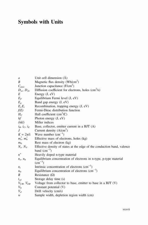
Symbols with Units
a Unit cell dimension (Å)B Magnetic flux density (Wb/cm2)Cjunc Junction capacitance (F/cm2)Dxe, Dxh Diffusion coefficient for electrons, holes (cm2/s)E Energy (J, eV)EF Equilibrium Fermi level (J, eV)Eg Band gap energy (J, eV)Er,Et Recombination, trapping energy (J, eV)f(E) Fermi-Dirac distribution functionHC Hall coefficient (cm3/C)hf Photon energy (J, eV)(hkl) Miller indicesiB, iC, iE Base, collector, emitter current in a BJT (A)J Current density (A/cm2)K = 2π/λ Wave number (cm−1)me*, mh
* Effective mass of electrons, holes (kg)m0 Rest mass of electron (kg)Nc, NV Effective density of states at the edge of the conduction band, valence
band (cm−3)n+ Heavily doped n-type materialne, nh Equilibrium concentration of electrons in n-type, p-type material
(cm−3)ni Intrinsic concentration of electrons (cm−3)n0 Equilibrium concentration of electrons (cm−3)R Resistance (Ω)tsd Storage delay time (s)VCB, VEB Voltage from collector to base, emitter to base in a BJT (V)V0 Constant potential (V)Vd Drift velocity (cm/s)w Sample width, depletion region width (cm)
xxxvii
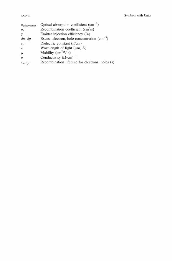
αabsorption Optical absorption coefficient (cm−1)αr Recombination coefficient (cm3/s)γ Emitter injection efficiency (%)δn, δp Excess electron, hole concentration (cm−3)εr Dielectric constant (F/cm)λ Wavelength of light (µm, Å)µ Mobility (cm2/V-s)σ Conductivity (Ω-cm)−1
τn, τp Recombination lifetime for electrons, holes (s)
xxxviii Symbols with Units
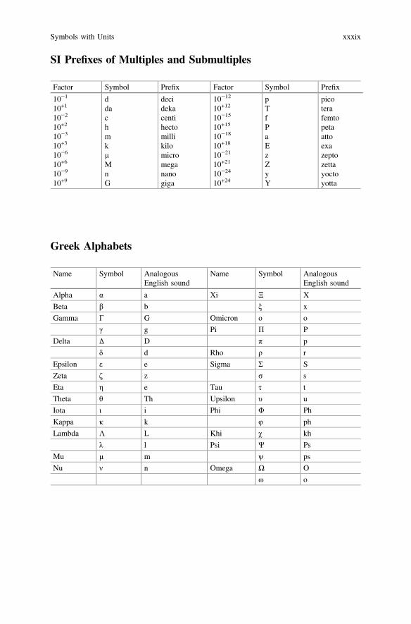
SI Prefixes of Multiples and Submultiples
Factor Symbol Prefix Factor Symbol Prefix
10−1
10+1
10−2
10+2
10−3
10+3
10−6
10+6
10−9
10+9
ddachmkµMnG
decidekacentihectomillikilomicromegananogiga
10−12
10+12
10−15
10+15
10−18
10+18
10−21
10+21
10−24
10+24
pTfPaEzZyY
picoterafemtopetaattoexazeptozettayoctoyotta
Greek Alphabets
Name Symbol AnalogousEnglish sound
Name Symbol AnalogousEnglish sound
Alpha α a Xi Ξ X
Beta β b ξ x
Gamma Γ G Omicron ο o
γ g Pi Π P
Delta Δ D π p
δ d Rho ρ r
Epsilon ε e Sigma Σ S
Zeta ζ z σ s
Eta η e Tau τ t
Theta θ Th Upsilon υ u
Iota ι i Phi Φ Ph
Kappa κ k φ ph
Lambda Λ L Khi χ kh
λ l Psi Ψ Ps
Mu µ m ψ ps
Nu ν n Omega Ω O
ω o
Symbols with Units xxxix
About the Authors
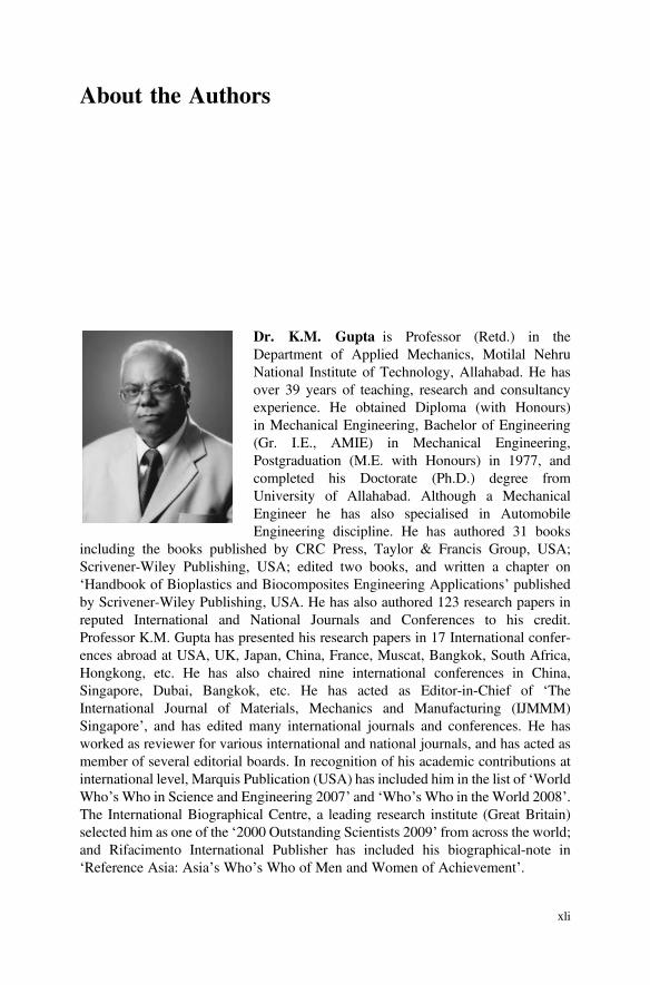
Dr. K.M. Gupta is Professor (Retd.) in theDepartment of Applied Mechanics, Motilal NehruNational Institute of Technology, Allahabad. He hasover 39 years of teaching, research and consultancyexperience. He obtained Diploma (with Honours)in Mechanical Engineering, Bachelor of Engineering(Gr. I.E., AMIE) in Mechanical Engineering,Postgraduation (M.E. with Honours) in 1977, andcompleted his Doctorate (Ph.D.) degree fromUniversity of Allahabad. Although a MechanicalEngineer he has also specialised in AutomobileEngineering discipline. He has authored 31 books
including the books published by CRC Press, Taylor & Francis Group, USA;Scrivener-Wiley Publishing, USA; edited two books, and written a chapter on‘Handbook of Bioplastics and Biocomposites Engineering Applications’ publishedby Scrivener-Wiley Publishing, USA. He has also authored 123 research papers inreputed International and National Journals and Conferences to his credit.Professor K.M. Gupta has presented his research papers in 17 International confer-ences abroad at USA, UK, Japan, China, France, Muscat, Bangkok, South Africa,Hongkong, etc. He has also chaired nine international conferences in China,Singapore, Dubai, Bangkok, etc. He has acted as Editor-in-Chief of ‘TheInternational Journal of Materials, Mechanics and Manufacturing (IJMMM)Singapore’, and has edited many international journals and conferences. He hasworked as reviewer for various international and national journals, and has acted asmember of several editorial boards. In recognition of his academic contributions atinternational level, Marquis Publication (USA) has included him in the list of ‘WorldWho’s Who in Science and Engineering 2007’ and ‘Who’s Who in the World 2008’.The International Biographical Centre, a leading research institute (Great Britain)selected him as one of the ‘2000 Outstanding Scientists 2009’ from across the world;and Rifacimento International Publisher has included his biographical-note in‘Reference Asia: Asia’s Who’s Who of Men and Women of Achievement’.
xli
Recipient of many Gold Medals and Prizes for his outstanding career fromDiploma to Doctorate (a rare achievement); he has served as Head of AutomobileEngineering Department at the Institute of Engineering and Rural Technology,Allahabad. He masterminded the development of several laboratories viz.Automobile related Labs, Materials Science Lab., Strength of Materials Lab.,Hydraulics Lab., etc., at different Institutes/colleges. He was the trail brazier inestablishing an Auto Garage and a Repairing Workshop.
Dr. K.M. Gupta has undergone several industrial trainings at many reputedindustries and workshops. He is endowed with vast experience in CurriculumDevelopment activities and consultancy. Earlier, he served as Dean of Research &Consultancy, Head of the Applied Mechanics Department at Motilal NehruNational Institute of Technology Allahabad. He has acted as Chairman of variousresearch selection committees, of research project monitoring committees and otheradministrative committees of his institute and other universities. He has also servedas Chairperson, Community Development Cell (CDC) of MNNIT for several years.
Presently, Dr. Gupta is teaching Materials Science, Engineering Mechanics,Electrical and Electronic Materials, Solid Mechanics, etc. His research interests arein the fields of materials science, composite materials, stress analysis, solidmechanics, etc.
Nishu Gupta is a Research Scholar in theDepartment of Electronics and CommunicationEngineering, Motilal Nehru National Institute ofTechnology Allahabad, India. He received his B.Tech. degree in Electronics and CommunicationEngineering from Uttar Pradesh Technical Universityand M. Tech. degree in Nanoscience and Technologyfrom Delhi Technological University (FormerelyDelhi College of Engineering), Delhi, India.
Earlier, he served as Software Engineer at InfosysTechnologies Limited. He has published 18 researchpapers to his credit which were published in various
international and national journals and conferences in India and abroad, includingfive papers in international journals. He has attended six international conferencesabroad. He is the recipient of honours and awards that include “Top 2000Intellectuals of the 21st century by International Biographical Centre, Cambridge,England”. Marquis Publication (USA) has included him in the list of ‘World Who’sWho in the world in the year 2009 and 2013 editions. He had been shortlisted bythe Ministry of HRD, Government of India for the CommonwealthScholarship/Fellowship Plan, 2012 offered by the Government of United Kingdom.
His research interests are in the field of semiconductor devices, hybrid solarcells, nano-communication networks and related fields.
xlii About the Authors