Energy Harvesting Technologies: Thick-Film Piezoelectric ......Energy Harvesting Technologies:...
26
8 Energy Harvesting Technologies: Thick-Film Piezoelectric Microgenerator Swee Leong Kok Faculty of Electronic and Computer Engineering, Universiti Teknikal Malaysia Melaka, Malaysia 1. Introduction With the advancement in the areas of wireless technology and low-power electronics, a pervasive system is made possible. This system is referred to a world where computational devices are embedded in the environment for intelligent buildings and home automation, autonomous vehicles and also possible to be implanted in human bodies such as the one in body sensor networks for health monitoring. To develop a totally autonomous system, however, traditional batteries, with limited life-span have to be replaced with energy harvesters, which can provide clean and renewable electrical energy sources. Vibration-based energy harvesting is one of the attractive solutions for powering autonomous microsystems, due to the fact that, vibration sources are ubiquitous in the ambient environment. Basically, the vibration-to-electricity conversion mechanism can be implemented by piezoelectric [1], electromagnetic [2], electrostatic [3], and magnetostrictive [4] transductions. In this thesis, piezoelectric transduction is investigated due to its high electrical output density, compatibility with conventional thick-film and thin-film fabrication technologies and ease of integration in silicon integrated circuits. Typically, piezoelectric materials are fabricated in the form of a cantilever structure, whereby stress is induced by bending the beam configuration in an oscillating manner and generating electric charges on its electrodes, as a result of the piezoelectric effect [5]. They are widely used as sensors and actuators [6, 7]. In recent years, piezoelectric materials are advancing into another level of development whereby they are used to provide an alternative for powering wireless sensor nodes through vibrations within the environment [1, 8, 9]. Typically, the piezoelectric materials are deposited on a non-electro-active substrate such as alumina, stainless steel or aluminium. They are physically clamped at one end to a rigid base and free to move at the other end. The presence of the substrate does not contribute directly to the electrical output, but merely serves as a mechanical supporting platform, which constrain the movement on the piezoelectric materials and poses difficulties for integration with other microelectronic devices. In order to minimise the constraint, a cantilever structure, which is free from external support or attachment to a non-electro- active platform is proposed. This structure would be in free-standing form consists of only www.intechopen.com
Transcript of Energy Harvesting Technologies: Thick-Film Piezoelectric ......Energy Harvesting Technologies:...
8
Energy Harvesting Technologies: Thick-Film Piezoelectric Microgenerator
Swee Leong Kok Faculty of Electronic and Computer Engineering,
Universiti Teknikal Malaysia Melaka, Malaysia
1. Introduction
With the advancement in the areas of wireless technology and low-power electronics, a pervasive system is made possible. This system is referred to a world where computational devices are embedded in the environment for intelligent buildings and home automation, autonomous vehicles and also possible to be implanted in human bodies such as the one in body sensor networks for health monitoring. To develop a totally autonomous system, however, traditional batteries, with limited life-span have to be replaced with energy harvesters, which can provide clean and renewable electrical energy sources.
Vibration-based energy harvesting is one of the attractive solutions for powering autonomous microsystems, due to the fact that, vibration sources are ubiquitous in the ambient environment. Basically, the vibration-to-electricity conversion mechanism can be implemented by piezoelectric [1], electromagnetic [2], electrostatic [3], and magnetostrictive [4] transductions. In this thesis, piezoelectric transduction is investigated due to its high electrical output density, compatibility with conventional thick-film and thin-film fabrication technologies and ease of integration in silicon integrated circuits.
Typically, piezoelectric materials are fabricated in the form of a cantilever structure, whereby stress is induced by bending the beam configuration in an oscillating manner and generating electric charges on its electrodes, as a result of the piezoelectric effect [5]. They are widely used as sensors and actuators [6, 7]. In recent years, piezoelectric materials are advancing into another level of development whereby they are used to provide an alternative for powering wireless sensor nodes through vibrations within the environment [1, 8, 9].
Typically, the piezoelectric materials are deposited on a non-electro-active substrate such as
alumina, stainless steel or aluminium. They are physically clamped at one end to a rigid
base and free to move at the other end. The presence of the substrate does not contribute
directly to the electrical output, but merely serves as a mechanical supporting platform,
which constrain the movement on the piezoelectric materials and poses difficulties for
integration with other microelectronic devices. In order to minimise the constraint, a
cantilever structure, which is free from external support or attachment to a non-electro-
active platform is proposed. This structure would be in free-standing form consists of only
www.intechopen.com
Sustainable Energy Harvesting Technologies – Past, Present and Future 192
the active piezoelectric materials and electrodes, and would be able to be stressed to
generate charges similar to the traditional cantilever structure.
Micro scale free-standing structures in the form of cantilever are commonly fabricated by using thick-film, thin-film and silicon micromachining technology [10]. However, thin-film and micromachining involves complex and expensive processes such as chemical vapour deposition and photolithography. Furthermore, the structures fabricated in these technologies generally are small (a few micrometers in length and width, and less than 1 μm thick) [11], therefore usually producing very low electrical output power (in order of nano-watts) and operate at high level of vibration (in order of kilohertz). The technology used for fabricating free-standing devices depends on the application, for example, in bio-molecular recognition [12], thin-film and micro-machining technologies are used to fabricate cantilevers with sub-micron dimensions. Thick-film technology is preferable to be used for fabricating bigger structures with thicknesses greater than 50 μm, and typically with area from a few mm2 to a few cm2, which is the size in between bulk devices and thin-film devices. Thick-film technology can be used to fill the gap between these technologies.
There are a number of challenges in the research of designing, fabricating and characterising free-standing thick-film piezoelectric cantilevers for energy harvesting. Firstly the research requires the understanding of the process conditions and limitation of thick-film technology particularly for fabricating three-dimensional structures. Thick-film technology involves processes which are hostile and destructive to ceramic free-standing structures e.g. high contact force (> 1 N) during screen-printing, high air flow curtain (> 50 l min-1) in multi-zone furnace and high thick-film processing temperature (> 800 °C). The thermal expansion coefficient mismatch between electrode and piezoelectric materials could also pose a problem in fabricating straight and flat cantilever. Besides that, the mechanical properties of thick-film ceramic materials are notoriously brittle and fragile which is poor to withstand the stress induced when the structure is operated in bending mode.
The target to meet the minimum electrical energy requirement for powering the microsystem is another surmounting challenge. Typically, a ceramic cantilever structure has high mechanical Q-factor at around 150, therefore, in order to harvest maximum electrical energy, the resonant frequency of the device has to match the ambient vibration sources. The unpredictable nature of ambient vibration sources intensifies the challenges toward making thick-film free-standing structures as a useful ambient energy harvester. All of these challenges will be addressed and suggested solutions to the issues will be discussed in detail in this thesis.
2. Piezoelectricity
Piezoelectricity is the ability of certain crystals to generate a voltage when a corresponding mechanical stress is applied. The piezoelectric effect is reversible, where the shape of the piezoelectric crystals will deform proportional to externally applied voltage.
Piezoelectricity was first discovered by the brothers Pierre Curie and Jacques Curie in 1880. They predicted and demonstrated that crystalline materials like tourmaline, quartz, topaz, cane sugar, and Rochelle salt (sodium potassium tartrate tetrahydrate) can generate electrical polarization from mechanical stress. Inverse piezoelectricity was mathematically deduced from fundamental thermodynamic principles by Lippmann in 1881. Later the Curies confirmed the existence of the inverse piezoelectric effect [13].
www.intechopen.com
Energy Harvesting Technologies: Thick-Film Piezoelectric Microgenerator 193
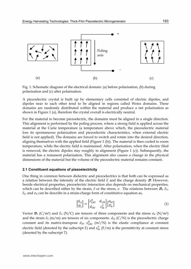
Fig. 1. Schematic diagram of the electrical domain: (a) before polarisation, (b) during polarisation and (c) after polarisation.
A piezoelectric crystal is built up by elementary cells consisted of electric dipoles, and dipoles near to each other tend to be aligned in regions called Weiss domains. These domains are randomly distributed within the material and produce a net polarisation as shown in Figure 1 (a), therefore the crystal overall is electrically neutral.
For the material to become piezoelectric, the domains must be aligned in a single direction.
This alignment is performed by the poling process, where a strong field is applied across the
material at the Curie temperature (a temperature above which, the piezoelectric material
loss its spontaneous polarization and piezoelectric characteristics, when external electric
field is not applied). The domains are forced to switch and rotate into the desired direction,
aligning themselves with the applied field (Figure 1 (b)). The material is then cooled to room
temperature, while the electric field is maintained. After polarisation, when the electric filed
is removed, the electric dipoles stay roughly in alignment (Figure 1 (c)). Subsequently, the
material has a remanent polarisation. This alignment also causes a change in the physical
dimensions of the material but the volume of the piezoelectric material remains constant.
2.1 Constituent equations of piezoelectricity
One thing in common between dielectric and piezoelectrics is that both can be expressed as a relation between the intensity of the electric field E and the charge density 錫. However, beside electrical properties, piezoelectric interaction also depends on mechanical properties, which can be described either by the strain, δ or the stress, σ. The relations between 錫i, Ek, δij, and σkl can be describe in a strain-charge form of constitutive equation as,
釆絞沈珍鴫沈 挽 = 峪嫌沈珍賃鎮帳 穴沈珍賃穴沈賃鎮 綱沈賃脹 崋 峙購賃鎮継賃 峩 (1)
Vector 錫i (C/m2) and Ek (N/C) are tensors of three components and the stress σkl (N/m2)
and the strain δij (m/m) are tensors of six components. dikl (C/N) is the piezoelectric charge
constant and its matrix-transpose dijk, 嫌沈珍賃鎮帳 (m2/N) is the elastic compliance at constant
electric field (denoted by the subscript E) and 綱沈賃脹 (F/m) is the permittivity at constant stress
(denoted by the subscript T).
Poling axis
(a) (b) (c)
+
−
www.intechopen.com
Sustainable Energy Harvesting Technologies – Past, Present and Future 194
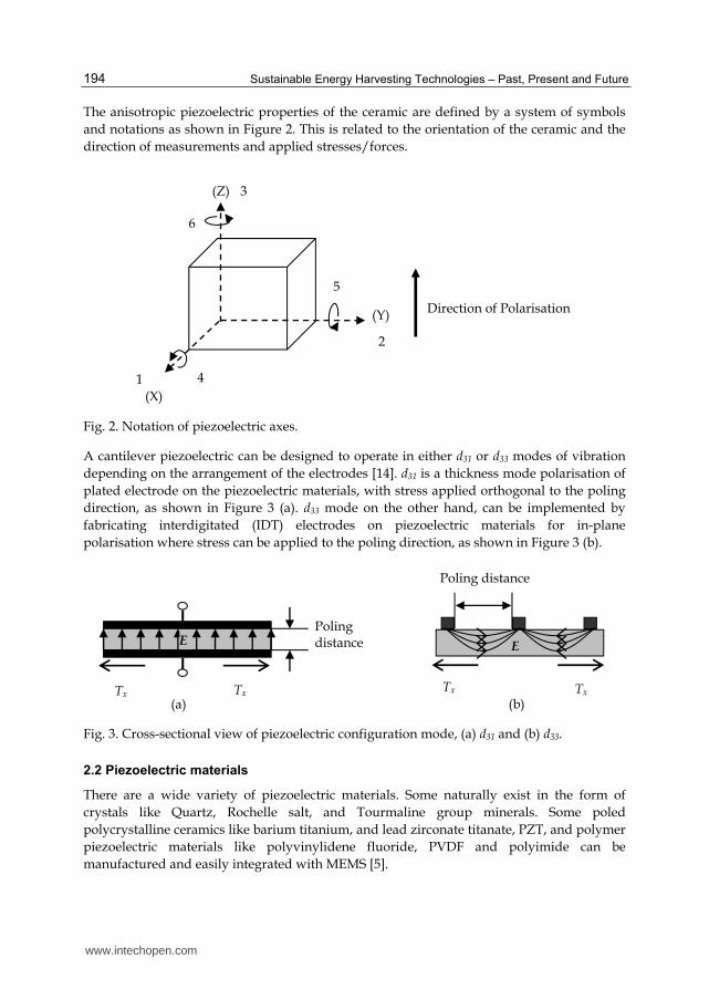
The anisotropic piezoelectric properties of the ceramic are defined by a system of symbols
and notations as shown in Figure 2. This is related to the orientation of the ceramic and the
direction of measurements and applied stresses/forces.
Fig. 2. Notation of piezoelectric axes.
A cantilever piezoelectric can be designed to operate in either d31 or d33 modes of vibration
depending on the arrangement of the electrodes [14]. d31 is a thickness mode polarisation of
plated electrode on the piezoelectric materials, with stress applied orthogonal to the poling
direction, as shown in Figure 3 (a). d33 mode on the other hand, can be implemented by
fabricating interdigitated (IDT) electrodes on piezoelectric materials for in-plane
polarisation where stress can be applied to the poling direction, as shown in Figure 3 (b).
Fig. 3. Cross-sectional view of piezoelectric configuration mode, (a) d31 and (b) d33.
2.2 Piezoelectric materials
There are a wide variety of piezoelectric materials. Some naturally exist in the form of
crystals like Quartz, Rochelle salt, and Tourmaline group minerals. Some poled
polycrystalline ceramics like barium titanium, and lead zirconate titanate, PZT, and polymer
piezoelectric materials like polyvinylidene fluoride, PVDF and polyimide can be
manufactured and easily integrated with MEMS [5].
(X)
(Y)
6
2
5
1 4
Direction of Polarisation
(Z) 3
E
Tx Tx
Poling distance
(a) (b)
Tx Tx
E
Poling distance
www.intechopen.com
Energy Harvesting Technologies: Thick-Film Piezoelectric Microgenerator 195
Commercially, piezoelectric materials are manufactured in bulk form. They are fabricated from a combination of ceramic materials (in short piezoceramics) and pressed in a high temperature (1100 – 17000C) to form a solid poly-crystalline structure. The raw material to fabricate bulk piezoelectric is in powder form. The powder is then pressed and formed into desired shapes and sizes, which is mechanically strong and dense [15]. In order to make these bulk ceramics into piezoelectric materials, electrodes are deposited onto their surface either by screen printing or vacuum deposition, and poled with electric fields of 2-8 MV·m-1 in an oil bath at a temperature of 130 - 220 0C [16]. Bulk piezoceramics are attractive for their high electromechanical efficiencies and high energy densities. However, bulk piezoceramics
tend to be relatively thick (greater than 100 μm), which will not be sensitive and need higher energies to actuate their structures, besides that they are difficult to be processed into
thickness below 100 μm, therefore limit their application in Micro-Electro-Mechanical System (MEMS). Furthermore they need to be attached to certain parts of the MEMS structures using mechanical or adhesive bonding, which is tedious and not cost effective.
MEMS devices which require piezoelectric structures with features below 100 μm would usually be fabricated using thin and thick film technologies.
Piezoelectric polymer materials are attractive in fabricating flexible devices. They have much higher piezoelectric stress constants and low elastic stiffness which give them advantages in producing high sensitivity sensors compared to brittle piezoceramics. However, these materials have lower piezoelectric charge constant and are not favourable to fabricate device for electrical power generation. Polyvinylidene fluoride (PVDF) is a common piezoelectric polymer material, which was discovered by Kawai [17]. It is lightweight, tough, and can be cut to form relatively large devices. The earlier form of PVDF was in polymer sheet, which is difficult to be shaped in micro-scale and they are usually processed with a punching technique based on a micro-embossing technique which is described in the literature [18]. With the development of PVDF thin-film technology, micro-structures can be fabricated as reported by Arshak et al [19]. The fabrication process
involved drying and curing at low temperature of around 170 °C, and was able to produce d33 of 24 pC/N1 [20]. An alternative to PVDF is polyimide, a high temperature piezoelectric polymer, which can maintain its piezoelectric properties at temperature up to 150 °C as reported by Atkinson et al [21].
Film piezoceramics have the advantages that lie between bulk and polymer piezoelectric
materials. Although film piezoceramics do not have piezoelectric activity as high as bulk
piezoceramics, however, for certain applications where a device thickness has to be
fabricated less than 100 μm, film piezoceramics are more favourable for their fabrication
compatibility with micro scale devices. Films can be deposited directly on to a substrate,
using a deposition technique that is more precise and with higher resolution. The processing
temperature of film piezoceramics is in between bulk piezoceramics and piezoelectric
polymers (800 °C – 1000 °C), which make it possible to be integrated with semiconductor
technology. Film piezoceramics basically can be fabricated with thin- and thick-film
technologies. Thin-film technologies involve physical vapour deposition, chemical vapour
deposition, and solution deposition, which fabricate films with typical thickness less than 5
μm. For thicker films (10 μm – 100 μm), thick-film technology is preferable. The technology
involves a screen printing method, where each layer of ceramic thick film will be printed on
a substrate followed by drying and curing processes.
www.intechopen.com
Sustainable Energy Harvesting Technologies – Past, Present and Future 196
2.3 Lead zirconate titanate (PZT)
Research and development in high performance piezoelectric ceramic had attracted great attention since the discovery of barium titanium oxide in 1940 [22]. This was followed by the discovery of lead titanate zirconate (PZT) in 1950s by Bernard Jaffe [23]. Compared to barium titanium oxide, PZT has a higher Curie point, higher total electric charge, and higher coercive voltage. PZT can be processed in bulk, thin-film, thick-film, and polymer forms in applications suited to their individual characteristics.
Thick-film PZT materials can be classified as ‘hard’ and ‘soft’, according to their coercive field during field-induced-strain actuation and Curie temperature [24]. A ‘hard’ piezoceramic has larger coercive field (greater than 1 kV/mm) and higher Curie point (TC >
250 °C) compared to ‘soft’ piezoceramic, which has moderate coercive field (between 0.1 and
1 kV/mm) and moderate Curie point (150 °C < TC < 250 °C) . Examples of ‘hard’ PZTs are Pz26 from Ferroperm Piezoceramics [16] and PZT-401 from Morgan Electroceramics [25]. Their typical applications are high power ultrasonics for cleaning, welding and drilling devices. Their distinctive characteristics include high mechanical factor, high coercive field, and low dielectric constant, which make them capable to be used in underwater applications and high voltage generators.
Compared to its counterpart, ‘Soft’ PZTs have lower mechanical Q-factor, higher electromechanical coupling coefficient, and higher dielectric constant, which are useful to fabricate sensitive receivers and applications requiring fine movement control, for instant in hydrophones and ink jet printers. Other applications ranging from combined resonant transducers (for medical and flow measurements) to accelerometer and pressure sensors [26]. Examples of soft PZTs are Pz27 and Pz29 from Ferroperm Piezoceramics. Pz27 and Pz29 have similar properties as PZT-5A and PZT-5H respectively from Morgan Electroceramics [25].
3. Vibration energy harvesting
Piezoelectric is one of the four general types of mechanical-to-electrical energy conversion
mechanisms for harvesting vibration energy [27]. The other three are electromagnetic [2],
electrostatic [3] and magnetostrictive [4]. With the improvement of piezoelectric activity, the
PZT piezoelectric materials (traditionally used to fabricate sensing devices) are becoming
popular in fabricating micro-power generators for the application of embedded and remote
systems [28]. Micro-generator is the term often used to describe a device which produces
electrical power in micro-Watt scale, while energy harvester is a more general term for
describing a device which produces power derived from external ambient sources (e.g.
solar, vibration, thermal and wind energy). Both of these terms will be used interchangeably
in this thesis where appropriate.
The vibration energy harvesting of piezoelectric materials is based on the concept of shunt damping to control mechanical vibration [29], however, rather than dissipating the energy through joule heating, the energy is used to power some electronic devices.
In order to estimate the output power from a vibration energy harvester, analytical models have been developed over the years. A generic energy conversion model followed by a specific conversion model for piezoelectric will be discussed in the following section.
www.intechopen.com
Energy Harvesting Technologies: Thick-Film Piezoelectric Microgenerator 197
3.1 Generic mechanical-to-electrical conversion model
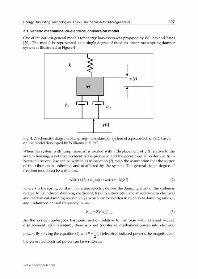
One of the earliest general models for energy harvesters was proposed by William and Yates
[30]. The model is represented as a single-degree-of-freedom linear mass-spring-damper
system as illustrated in Figure 4
Fig. 4. A schematic diagram of a spring-mass-damper system of a piezoelectric FSD, based on the model developed by Williams et al [30].
When the system with lump mass, M is excited with a displacement of y(t) relative to the
system housing, a net displacement z(t) is produced and the generic equation derived from
Newton’s second law can be written as in equation (2), with the assumption that the source
of the vibration is unlimited and unaffected by the system. The general single degree of
freedom model can be written as,
( )( ) ( ) ( ) ( )e mMz t b b z t z t My tκ+ + + = −$$ $ $$ (2)
where κ is the spring constant. For a piezoelectric device, the damping effect of the system is
related to its induced damping coefficient, b (with subscripts e and m referring to electrical
and mechanical damping respectively), which can be written in relation to damping ratios, ζ
and undamped natural frequency, ωn as,
, ,2e m n e mb Mω ζ= (3)
As the system undergoes harmonic motion relative to the base with external excited
displacement ( ) sin( )y t Y tω= , there is a net transfer of mechanical power into electrical
power. By solving the equation (2) and1
2eP b z= $ (electrical induced power), the magnitude of
the generated electrical power can be written as,
k
z (t)
y(t)
be bm
M
www.intechopen.com
Sustainable Energy Harvesting Technologies – Past, Present and Future 198
3
3 2
22 2
2 1
en
Tn n
M Y
P
ωζ ω ωω ωζ ω ω
⎛ ⎞⎜ ⎟⎝ ⎠= ⎡ ⎤⎡ ⎤⎛ ⎞ ⎛ ⎞⎢ ⎥+ −⎢ ⎥⎜ ⎟ ⎜ ⎟⎢ ⎥⎢ ⎥⎝ ⎠ ⎝ ⎠⎣ ⎦ ⎣ ⎦
(4)
where ζT is the total damping ratio (ζT = ζe + ζm), and ω is the base excited angular frequency and Y is the amplitude of vibration. When the device is operated at its resonant frequency ωn, maximum power can be produced and equation (4) is simplified to,
( )2
max 24
e in
n e m
M aP
ζω ζ ζ= + (5)
where ain is input acceleration from vibration source ( 2in na Yω= ). This equation shows that
input acceleration is the major factor for increasing the output power from the piezoelectric
FSDs. By maintaining the frequency of the vibration source to match the natural frequency
of the device, the electric power generated by the device is proportional to the square of the
source acceleration.
3.2 Analytical model of piezoelectric harvester
Although the mass-spring-damper system with lumped parameters is more suitable to represent a simple electromagnetic vibration-to-electric energy conversion model, it gives an insight of a general mechanism of mechanical to electrical transduction model which include piezoelectric transduction.
A more specific piezoelectric energy harvester model, where the mechanism of piezoelectric transduction due to the constitutive relations according to equation (1) is taken into account, has been proposed by duToit et al [31], with an additional term related to undamped natural
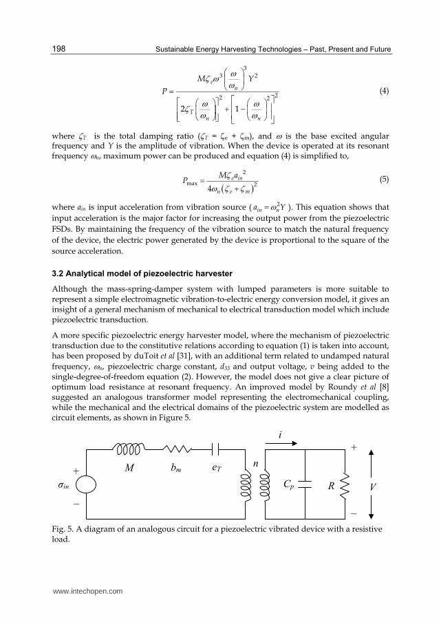
frequency, ωn, piezoelectric charge constant, d33 and output voltage, v being added to the single-degree-of-freedom equation (2). However, the model does not give a clear picture of optimum load resistance at resonant frequency. An improved model by Roundy et al [8] suggested an analogous transformer model representing the electromechanical coupling, while the mechanical and the electrical domains of the piezoelectric system are modelled as circuit elements, as shown in Figure 5.
Fig. 5. A diagram of an analogous circuit for a piezoelectric vibrated device with a resistive load.
www.intechopen.com
Energy Harvesting Technologies: Thick-Film Piezoelectric Microgenerator 199
The mechanical domain of the equivalent circuit consists of inductor, resistor and capacitor which represents the mass of the generator, M, the mechanical damping, bm, and mechanical stiffness, eT respectively. At the electrical domain, Cp is the capacitance of the piezoelectric and R is the external resistive load, while n is the equivalent turn ratio of the transformer which is proportional to the piezoelectric charge constant d31. V is the voltage across the piezoelectric and i is the current flow into the circuit, which are analogues to the stress and the strain rate respectively. The output voltage at resonant frequency derived from the model is,
( )31
2 2 2 2 221 12 1
p pin
T rr T r r
p p p
e d h Bj a
V
j kRC RC RC
ω εζ ωω ζ ω ω ω ω ω
−= ⎡ ⎤⎛ ⎞ ⎡ ⎤⎢ ⎥− ⎜ + ⎟ + + + −⎢ ⎥⎜ ⎟⎢ ⎥ ⎢ ⎥⎝ ⎠ ⎣ ⎦⎣ ⎦
(6)
where j is the imaginary number, ω is the driving frequency (Hz), ωr is the fundamental resonant frequency of the cantilever (Hz), ET is the elastic constant for the composite structure (N/m2), d31 is the piezoelectric charge coefficient (C/N), hP is the thickness of the piezoelectric material, ε is the dielectric constant of the piezoelectric material (F), B is a constant related to the distance from the piezoelectric layer to the neutral axis of the structure, ζT is the total damping ratio, k31 is the piezoelectric coupling factor and CP is the capacitance of the piezoelectric material. The root mean square (rms) power is given as V2/ 2R, therefore from equation (6), the rms value of power transferred to the resistive load can be written as,
( )( ) ( )2
2 231
2 22 4 2 231 31
1
4 4 4
t PP in
r T P r T P r T
e d h BRC a
Pk RC k RC
εω ζ ω ζ ω ζ
⎛ ⎞⎜ ⎟⎝ ⎠= + + + (7)
More complex models have been developed by Erturk and Inman [32, 33]. Instead of a
single-degree-of-freedom model, they had developed a distributed parameter
electromechanical model which incorporates Euler-Bernoulli beam theory with the
piezoelectric constitutive equation. The detail of this model will not be discussed in this
research work. However, both models agree to a certain extent that at resonant frequency,
the output power is proportional to the square power of the piezoelectric charge coefficient,
the elasticity of the cantilever, the thickness of the piezoelectric material and the effective
mass of the cantilever, all but the first of which are controllable by design. It is also found
that the input acceleration from base excitation, ain (2
in na Yω= ) plays an important part in
output power generation. However, for the application of energy harvesters, the
acceleration level from an ambient vibration source is a natural phenomenon, which is not
controllable. Therefore the energy harvester has to be designed to suit the specific
application, though the model gives a good estimation for the potential power generation.
3.3 Cantilever-based piezoelectric energy harvesters
The most common piezoelectric energy harvesters are in the form of a cantilever, due to its simple geometry design and relative ease of fabrication. The structures usually consist of a
www.intechopen.com
Sustainable Energy Harvesting Technologies – Past, Present and Future 200
strong flexible supporting platform with one end fixed to the base on the substrate. Piezoelectric materials are deposited on either one side (unimorph) or both sides (bimorph) of the platform with the intention to strain the piezoelectric films and generate charges from the piezoelectric d31 effect. This bending mode operation is effectively generating electrical energy when they are exposed to continuous harmonic vibration sources.
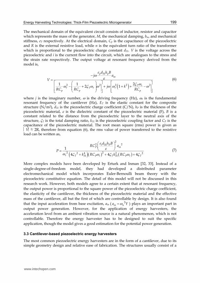
The flexible supporting platform is not electrically active but acts as a mechanical support to the whole structure. It can be stainless steel, aluminium plate or micromachined silicon depending on the fabrication process and the scale of the device. One of the earliest examples using stainless steel as the supporting platform was developed by Glynne-Jones et al [1]. They developed a cantilever with a tapered profile as shown in Figure 6, in order to produce constant strain in the piezoelectric film along its length for a given displacement. The generator was fabricated by screen-printing a layer of PZT-5H with a thickness of 70 µm on both sides of a stainless steel beam with length 23 mm and thickness 100 µm to form a bimorph cantilever. The device was found to operate at its resonant frequency of 80.1 Hz and produced up to 3 µW of power when driving an optimum resistive load of 333 kΩ.
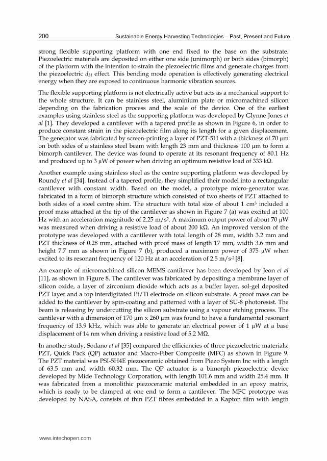
Another example using stainless steel as the centre supporting platform was developed by
Roundy et al [34]. Instead of a tapered profile, they simplified their model into a rectangular
cantilever with constant width. Based on the model, a prototype micro-generator was
fabricated in a form of bimorph structure which consisted of two sheets of PZT attached to
both sides of a steel centre shim. The structure with total size of about 1 cm3 included a
proof mass attached at the tip of the cantilever as shown in Figure 7 (a) was excited at 100
Hz with an acceleration magnitude of 2.25 m/s2. A maximum output power of about 70 µW
was measured when driving a resistive load of about 200 kΩ. An improved version of the
prototype was developed with a cantilever with total length of 28 mm, width 3.2 mm and
PZT thickness of 0.28 mm, attached with proof mass of length 17 mm, width 3.6 mm and
height 7.7 mm as shown in Figure 7 (b), produced a maximum power of 375 µW when
excited to its resonant frequency of 120 Hz at an acceleration of 2.5 m/s-2 [8].
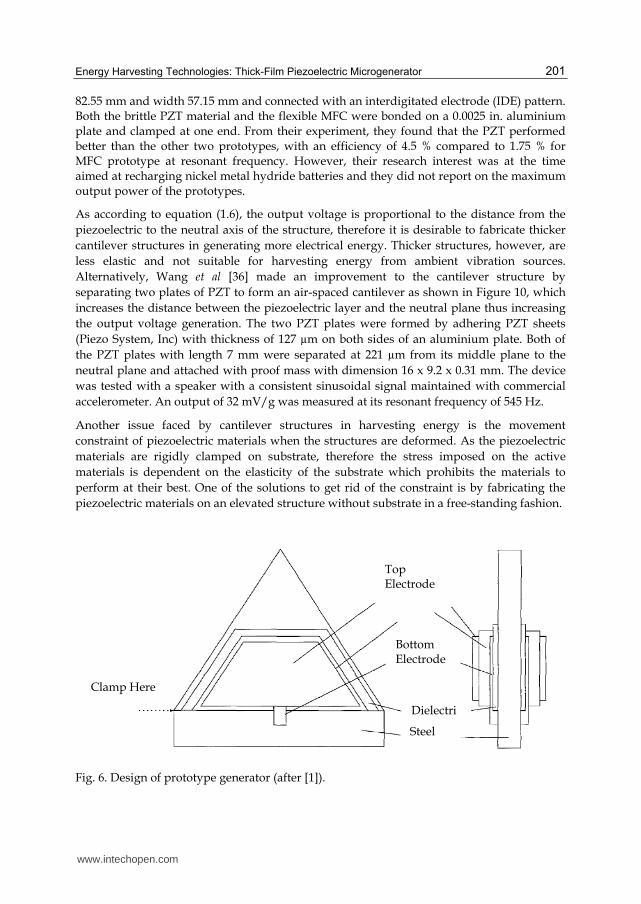
An example of micromachined silicon MEMS cantilever has been developed by Jeon et al
[11], as shown in Figure 8. The cantilever was fabricated by depositing a membrane layer of
silicon oxide, a layer of zirconium dioxide which acts as a buffer layer, sol-gel deposited
PZT layer and a top interdigitated Pt/Ti electrode on silicon substrate. A proof mass can be
added to the cantilever by spin-coating and patterned with a layer of SU-8 photoresist. The
beam is releasing by undercutting the silicon substrate using a vapour etching process. The
cantilever with a dimension of 170 µm x 260 µm was found to have a fundamental resonant
frequency of 13.9 kHz, which was able to generate an electrical power of 1 µW at a base
displacement of 14 nm when driving a resistive load of 5.2 MΩ.
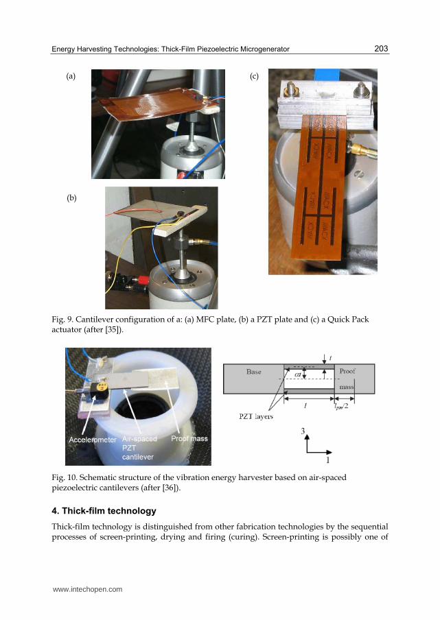
In another study, Sodano et al [35] compared the efficiencies of three piezoelectric materials: PZT, Quick Pack (QP) actuator and Macro-Fiber Composite (MFC) as shown in Figure 9. The PZT material was PSI-5H4E piezoceramic obtained from Piezo System Inc with a length of 63.5 mm and width 60.32 mm. The QP actuator is a bimorph piezoelectric device developed by Mide Technology Corporation, with length 101.6 mm and width 25.4 mm. It was fabricated from a monolithic piezoceramic material embedded in an epoxy matrix, which is ready to be clamped at one end to form a cantilever. The MFC prototype was developed by NASA, consists of thin PZT fibres embedded in a Kapton film with length
www.intechopen.com
Energy Harvesting Technologies: Thick-Film Piezoelectric Microgenerator 201
82.55 mm and width 57.15 mm and connected with an interdigitated electrode (IDE) pattern. Both the brittle PZT material and the flexible MFC were bonded on a 0.0025 in. aluminium plate and clamped at one end. From their experiment, they found that the PZT performed better than the other two prototypes, with an efficiency of 4.5 % compared to 1.75 % for MFC prototype at resonant frequency. However, their research interest was at the time aimed at recharging nickel metal hydride batteries and they did not report on the maximum output power of the prototypes.
As according to equation (1.6), the output voltage is proportional to the distance from the
piezoelectric to the neutral axis of the structure, therefore it is desirable to fabricate thicker
cantilever structures in generating more electrical energy. Thicker structures, however, are
less elastic and not suitable for harvesting energy from ambient vibration sources.
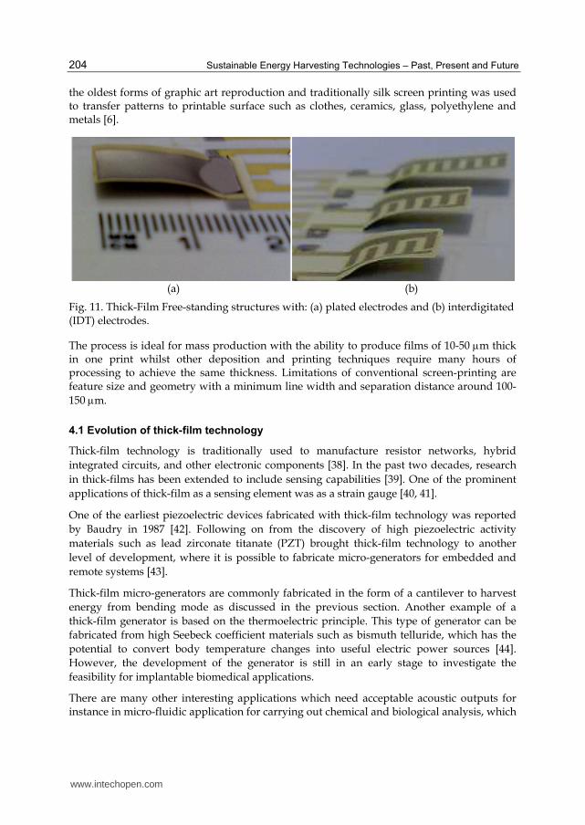
Alternatively, Wang et al [36] made an improvement to the cantilever structure by
separating two plates of PZT to form an air-spaced cantilever as shown in Figure 10, which
increases the distance between the piezoelectric layer and the neutral plane thus increasing
the output voltage generation. The two PZT plates were formed by adhering PZT sheets
(Piezo System, Inc) with thickness of 127 µm on both sides of an aluminium plate. Both of
the PZT plates with length 7 mm were separated at 221 µm from its middle plane to the
neutral plane and attached with proof mass with dimension 16 x 9.2 x 0.31 mm. The device
was tested with a speaker with a consistent sinusoidal signal maintained with commercial
accelerometer. An output of 32 mV/g was measured at its resonant frequency of 545 Hz.
Another issue faced by cantilever structures in harvesting energy is the movement
constraint of piezoelectric materials when the structures are deformed. As the piezoelectric
materials are rigidly clamped on substrate, therefore the stress imposed on the active
materials is dependent on the elasticity of the substrate which prohibits the materials to
perform at their best. One of the solutions to get rid of the constraint is by fabricating the
piezoelectric materials on an elevated structure without substrate in a free-standing fashion.
Fig. 6. Design of prototype generator (after [1]).
Clamp Here
Top Electrode
Bottom Electrode
Dielectri
Steel
www.intechopen.com
Sustainable Energy Harvesting Technologies – Past, Present and Future 202
Fig. 7. A A rectangular cantilever microgenerator prototype (b) An improved version (after [8]).
Fig. 8. MEMS micromachined IDE pattern cantilever (after [11]).
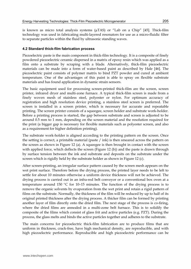
3.4 Free-standing cantilever structures
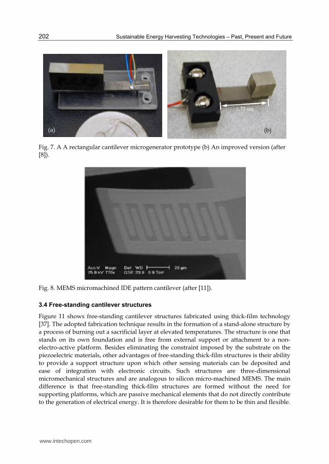
Figure 11 shows free-standing cantilever structures fabricated using thick-film technology
[37]. The adopted fabrication technique results in the formation of a stand-alone structure by
a process of burning out a sacrificial layer at elevated temperatures. The structure is one that
stands on its own foundation and is free from external support or attachment to a non-
electro-active platform. Besides eliminating the constraint imposed by the substrate on the
piezoelectric materials, other advantages of free-standing thick-film structures is their ability
to provide a support structure upon which other sensing materials can be deposited and
ease of integration with electronic circuits. Such structures are three-dimensional
micromechanical structures and are analogous to silicon micro-machined MEMS. The main
difference is that free-standing thick-film structures are formed without the need for
supporting platforms, which are passive mechanical elements that do not directly contribute
to the generation of electrical energy. It is therefore desirable for them to be thin and flexible.
(a) (b)
www.intechopen.com
Energy Harvesting Technologies: Thick-Film Piezoelectric Microgenerator 203
Fig. 9. Cantilever configuration of a: (a) MFC plate, (b) a PZT plate and (c) a Quick Pack actuator (after [35]).
Fig. 10. Schematic structure of the vibration energy harvester based on air-spaced piezoelectric cantilevers (after [36]).
4. Thick-film technology
Thick-film technology is distinguished from other fabrication technologies by the sequential processes of screen-printing, drying and firing (curing). Screen-printing is possibly one of
(a)
(b)
(c)
www.intechopen.com
Sustainable Energy Harvesting Technologies – Past, Present and Future 204
the oldest forms of graphic art reproduction and traditionally silk screen printing was used to transfer patterns to printable surface such as clothes, ceramics, glass, polyethylene and metals [6].
(a) (b)
Fig. 11. Thick-Film Free-standing structures with: (a) plated electrodes and (b) interdigitated (IDT) electrodes.
The process is ideal for mass production with the ability to produce films of 10-50 μm thick in one print whilst other deposition and printing techniques require many hours of processing to achieve the same thickness. Limitations of conventional screen-printing are feature size and geometry with a minimum line width and separation distance around 100-
150 μm.
4.1 Evolution of thick-film technology
Thick-film technology is traditionally used to manufacture resistor networks, hybrid
integrated circuits, and other electronic components [38]. In the past two decades, research
in thick-films has been extended to include sensing capabilities [39]. One of the prominent
applications of thick-film as a sensing element was as a strain gauge [40, 41].
One of the earliest piezoelectric devices fabricated with thick-film technology was reported
by Baudry in 1987 [42]. Following on from the discovery of high piezoelectric activity
materials such as lead zirconate titanate (PZT) brought thick-film technology to another
level of development, where it is possible to fabricate micro-generators for embedded and
remote systems [43].
Thick-film micro-generators are commonly fabricated in the form of a cantilever to harvest
energy from bending mode as discussed in the previous section. Another example of a
thick-film generator is based on the thermoelectric principle. This type of generator can be
fabricated from high Seebeck coefficient materials such as bismuth telluride, which has the
potential to convert body temperature changes into useful electric power sources [44].
However, the development of the generator is still in an early stage to investigate the
feasibility for implantable biomedical applications.
There are many other interesting applications which need acceptable acoustic outputs for instance in micro-fluidic application for carrying out chemical and biological analysis, which
www.intechopen.com
Energy Harvesting Technologies: Thick-Film Piezoelectric Microgenerator 205
is known as micro total analysis systems (µTAS) or “Lab on a Chip” [45]. Thick-film technology was used in fabricating multi-layered resonators for use as a micro-fluidic filter to separate particles within the fluid by ultrasonic standing waves.
4.2 Standard thick-film fabrication process
Piezoelectric paste is the main component in thick-film technology. It is a composite of finely powdered piezoelectric ceramic dispersed in a matrix of epoxy resin which was applied as a film onto a substrate by scraping with a blade. Alternatively, thick-film piezoelectric materials can be made into a form of water-based paint as described by Hale [46]. The piezoelectric paint consists of polymer matrix to bind PZT powder and cured at ambient temperature. One of the advantages of this paint is able to spray on flexible substrate materials and has found application in dynamic strain sensors.
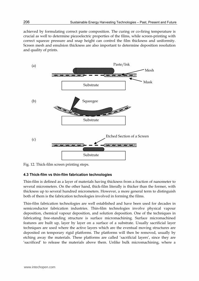
The basic equipment used for processing screen-printed thick-film are the screen, screen printer, infrared dryer and multi-zone furnace. A typical thick-film screen is made from a finely woven mesh of stainless steel, polyester or nylon. For optimum accuracy of registration and high resolution device printing, a stainless steel screen is preferred. The screen is installed in a screen printer, which is necessary for accurate and repeatable printing. The screen printer consists of a squeegee, screen holder and substrate work-holder. Before a printing process is started, the gap between substrate and screen is adjusted to be around 0.5 mm to 1 mm, depending on the screen material and the resolution required for the print (a bigger gap is necessary for flexible materials such as polyester screen, and also as a requirement for higher definition printing).
The substrate work-holder is aligned according to the printing pattern on the screen. Once
the setting is correct, a printable material (paste / ink) is then smeared across the pattern on
the screen as shown in Figure 12 (a). A squeegee is then brought in contact with the screen
with applied force, which deflects the screen (Figure 12 (b)) and the paste is drawn through
by surface tension between the ink and substrate and deposits on the substrate under the
screen which is rigidly held by the substrate holder as shown in Figure 12 (c).
After screen-printing, an irregular surface pattern caused by the screen mesh appears on the
wet print surface. Therefore before the drying process, the printed layer needs to be left to
settle for about 10 minutes otherwise a uniform device thickness will not be achieved. The
drying process is carried out in an infra-red belt conveyor or a conventional box oven at a
temperature around 150 °C for 10–15 minutes. The function of the drying process is to
remove the organic solvents by evaporation from the wet print and retain a rigid pattern of
films on the substrate. Normally, the thickness of the film will be reduced by up to half of its
original printed thickness after the drying process. A thicker film can be formed by printing
another layer of film directly onto the dried film. The next stage of the process is co-firing,
where the dried films are annealed in a multi-zone belt furnace. This is to solidify the
composite of the films which consist of glass frit and active particles (e.g. PZT). During the
process, the glass melts and binds the active particles together and adheres to the substrate.
The main concerns for piezoelectric thick-film fabrication are to produce films that are uniform in thickness, crack-free, have high mechanical density, are reproducible, and with high piezoelectric performance. Reproducible and high piezoelectric performance can be
www.intechopen.com
Sustainable Energy Harvesting Technologies – Past, Present and Future 206
achieved by formulating correct paste composition. The curing or co-firing temperature is crucial as well to determine piezoelectric properties of the films, while screen-printing with correct squeeze pressure and snap height can control the film thickness and uniformity. Screen mesh and emulsion thickness are also important to determine deposition resolution and quality of prints.
Fig. 12. Thick-film screen printing steps.
4.3 Thick-film vs thin-film fabrication technologies
Thin-film is defined as a layer of materials having thickness from a fraction of nanometer to
several micrometers. On the other hand, thick-film literally is thicker than the former, with
thickness up to several hundred micrometers. However, a more general term to distinguish
both of them is the fabrication technologies involved in forming the films.
Thin-film fabrication technologies are well established and have been used for decades in
semiconductor fabrication industries. Thin-film technologies involve physical vapour
deposition, chemical vapour deposition, and solution deposition. One of the techniques in
fabricating free-standing structure is surface micromachining. Surface micromachined
features are built up, layer by layer on a surface of a substrate. Usually sacrificial layer
techniques are used where the active layers which are the eventual moving structures are
deposited on temporary rigid platforms. The platforms will then be removed, usually by
etching away the materials. These platforms are called ‘sacrificial layers’, since they are
‘sacrificed’ to release the materials above them. Unlike bulk micromachining, where a
Paste/Ink
Mesh
Mask Substrate
Substrate
Squeegee
Etched Section of a Screen
Substrate
(a)
(b)
(c)
www.intechopen.com
Energy Harvesting Technologies: Thick-Film Piezoelectric Microgenerator 207
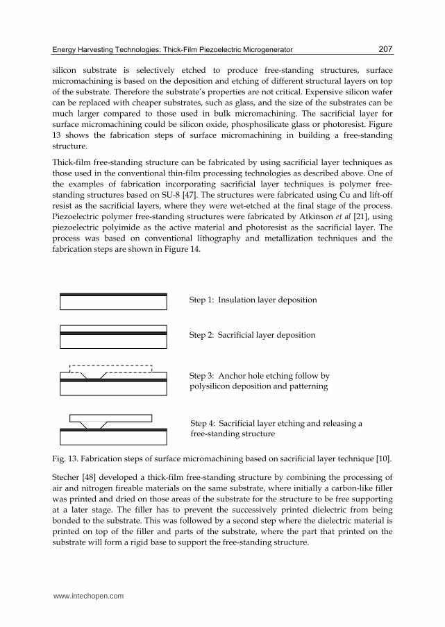
silicon substrate is selectively etched to produce free-standing structures, surface
micromachining is based on the deposition and etching of different structural layers on top
of the substrate. Therefore the substrate’s properties are not critical. Expensive silicon wafer
can be replaced with cheaper substrates, such as glass, and the size of the substrates can be
much larger compared to those used in bulk micromachining. The sacrificial layer for
surface micromachining could be silicon oxide, phosphosilicate glass or photoresist. Figure
13 shows the fabrication steps of surface micromachining in building a free-standing
structure.
Thick-film free-standing structure can be fabricated by using sacrificial layer techniques as
those used in the conventional thin-film processing technologies as described above. One of
the examples of fabrication incorporating sacrificial layer techniques is polymer free-
standing structures based on SU-8 [47]. The structures were fabricated using Cu and lift-off
resist as the sacrificial layers, where they were wet-etched at the final stage of the process.
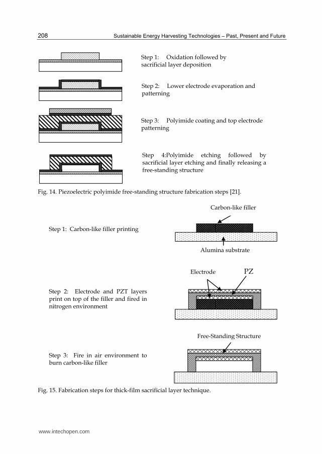
Piezoelectric polymer free-standing structures were fabricated by Atkinson et al [21], using
piezoelectric polyimide as the active material and photoresist as the sacrificial layer. The
process was based on conventional lithography and metallization techniques and the
fabrication steps are shown in Figure 14.
Fig. 13. Fabrication steps of surface micromachining based on sacrificial layer technique [10].
Stecher [48] developed a thick-film free-standing structure by combining the processing of
air and nitrogen fireable materials on the same substrate, where initially a carbon-like filler
was printed and dried on those areas of the substrate for the structure to be free supporting
at a later stage. The filler has to prevent the successively printed dielectric from being
bonded to the substrate. This was followed by a second step where the dielectric material is
printed on top of the filler and parts of the substrate, where the part that printed on the
substrate will form a rigid base to support the free-standing structure.
Step 1: Insulation layer deposition
Step 2: Sacrificial layer deposition
Step 3: Anchor hole etching follow by polysilicon deposition and patterning
Step 4: Sacrificial layer etching and releasing a free-standing structure
www.intechopen.com
Sustainable Energy Harvesting Technologies – Past, Present and Future 208
Fig. 14. Piezoelectric polyimide free-standing structure fabrication steps [21].
Fig. 15. Fabrication steps for thick-film sacrificial layer technique.
Step 1: Oxidation followed by sacrificial layer deposition
Step 2: Lower electrode evaporation and patterning
Step 3: Polyimide coating and top electrode patterning
Step 4:Polyimide etching followed by sacrificial layer etching and finally releasing a free-standing structure
Alumina substrate
Carbon-like filler
Step 1: Carbon-like filler printing
Step 2: Electrode and PZT layers print on top of the filler and fired in nitrogen environment
Electrode PZT
Step 3: Fire in air environment to burn carbon-like filler
Free-Standing Structure
www.intechopen.com
Energy Harvesting Technologies: Thick-Film Piezoelectric Microgenerator 209
The dried paste is then co-fired in a nitrogen atmosphere. The nitrogen must be used because the filler must not be burnt out before the glass-ceramic has sintered. The process is repeated to form a multilayer composite film. Finally, the composite film is co-fired in an air environment, where the carbon filler acting as a sacrificial layer is burnt out without residues, releasing a composite thick-film free-standing structure. The fabrication steps are shown in Figure 15. Similarly, the proposed free-standing energy harvester structures as described in section 3.4 can be fabricated using this technique.
5. Energy harvesters performance comparison
Over the years, many micro-generator prototypes have been fabricated. The most common vibration energy harvester is based on an electromagnetic principle because at present, the output powers produced by electromagnetic generators are greater than piezoelectric and electrostatic based generators. However, with recent improvement in piezoelectric activity in PZT and the ability to be incorporated within simple cantilever structures, which is relatively easy to be fabricated and integrated with microelectronic systems, piezoelectric methods are an attractive alternative for future investigation.
Each of the energy harvesters was being claimed to demonstrate better performance in one way than another. The most common comparison merit is the electrical output power density. Although power density comparison can give an idea of the performance of an energy harvester, it does not explain the influence of the excitation source. As according to Equation (5), the output power of a resonant device is closely dependent on the amplitude of an excitation source. However, to make the comparison meaningful, all the energy harvesters have to be excited at a fixed vibration characteristic (e.g. adjust acceleration level at resonant frequency of the tested devices to give a fixed vibration amplitude), which is impossible as the size of the energy harvesters range from micro to centimetre scales depending on the fabrication technology. Micro-scale devices are more sensitive to micro-scale vibration amplitudes (a few nano- to micrometer), while centimetre scale devices do not show their optimum performances if excited at these same levels, therefore it is not appropriate to make a comparison in terms of power density.
There are other alternative ways to compare the energy harvesters in a more universal
metric, for example, a normalised power density (NPD) suggested by Beeby et al [2], in
which the power density is divided by the source acceleration amplitude squared. Volume
figure of merit, FoMV, suggested by Mitcheson et al [49], measures the performance as a
percentage comparison to its maximum possible output for a particular device. The
maximum possible output is proportional to the resonant frequency of the device to the
power of three and the overall size of a device with an assumption that the device (with a
proof mass) has the density of gold, occupying half of the total volume and the other half is
room for displacement,
4/3 3
0
Measured Power Output
1
16
V
AU
FoM
Y Volρ ω= (8)
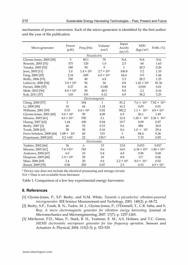
A few recently published experimental results of fabricated energy harvesters are listed and
summarised in Table 2.1. The table is divided into three sections according to the
www.intechopen.com
Sustainable Energy Harvesting Technologies – Past, Present and Future 210
mechanism of power conversion. Each of the micro-generator is identified by the first author
and the year of the publication.
Micro-generator Power
(μW) Freq (Hz)
Volume* (cm3)
Input Acceln (m/s2)
NPD (kgs/m3)
FoMV (%)
Piezoelectric
Glynne-Jones, 2000 [50] 3 80.1 70 NA NA NA Roundy, 2003 [51] 375 120 1.0 2.5 60 1.65 Tanaka, 2005 [52] 180 50 9 1 20.5 0.26 Jeon, 2005 [11] 1.0 1.4 × 10⁴ 2.7 × 10⁻⁵ 106.8 3.2 1.10 Fang, 2006 [20] 2.16 609 6.0 × 10⁻⁴ 64.4 0.9 1.44 Reilly, 2006 [53] 700 40 4.8 2.3 28.2 1.25 Lefeuvre, 2006 [54] 3.0 × 10⁵ 56 34 0.8 1.42 × 10⁴ 81.36 Ferrari, 2006 [55] 0.27 41 0.188 8.8 0.018 0.01 Mide, 2010 [56] 8.0 × 10³ 50 40.5 9.8 2.1 0.16 Kok, 2011 [37] 110 155 0.12 4.9 38.2 3.23
Electromagnetic
Ching, 2000 [57] 5 104 1 81.2 7.6 × 10⁻⁴ 7.82 × 10⁻⁴
Li, 2000 [58] 10 64 1.24 16.2 0.03 0.01 Williams, 2001 [59] 0.33 4.4 × 10³ 0.02 382.2 1.1 × 10⁻⁴ 4.8 × 10⁻⁵ Glynne-Jones, 2001 [60] 5.0 × 10³ 99 4.08 6.9 26.1 1.49 Mizuno, 2003 [61] 4.0 × 10⁻⁴ 700 2.1 12.4 1.24 × 10⁻⁶ 2.26 × 10⁻⁸ Huang, 2007 [62] 1.44 100 0.04 19.7 0.09 0.07 Beeby, 2007 [2] 46 52 0.15 0.6 884 24.8 Torah, 2008 [63] 58 50 0.16 0.6 1.0 × 10³ 29.4 Ferro Solution, 2008 [64] 1.08 × 10⁴ 60 133 1 84.4 0.36 Perpetuum, 2009 [65] 9.2 ×10⁴ 22 130.7 9.8 7.33 0.85
Electrostatic
Tashiro, 2002 [66] 36 6 15 12.8 0.015 0.017 Mizuno, 2003 [61] 7.4 ×10⁻⁶ 743 0.6 14.0 6.34 × 10⁻⁸ 1.86 × 10⁻⁹ Arakawa, 2004 [67] 6.0 10 0.4 4.0 0.96 0.68 Despesse, 2005 [68] 1.0 × 10³ 50 18 8.8 0.7 0.06 Miao, 2006 [69] 2.4 20 0.6 2.2 × 10³ 8.0 × 10⁻⁷ 0.02 Basset, 2009 [70] 0.06 250 0.07 2.5 0.15 4.9 × 10⁻³
* Device size does not include the electrical possessing and storage circuits NA = Data is not available from literature
Table 1. Comparison of a few key experimental energy harvesters.
6. References
[1] Glynne-Jones, P., S.P. Beeby, and N.M. White, Towards a piezoelectric vibration-powered microgenerator. IEE Science Measurement and Technlogy, 2001. 148(2): p. 68-72.
[2] Beeby, S.P., Torah, R. N., Tudor, M. J., Glynne-Jones, P., O'Donnell, T., C.R. Saha, and S. Roy, A micro electromagnetic generator for vibration energy harvesting. Journal of Micromechanics and Microengineering, 2007. 17(7): p. 1257-1265.
[3] Mitcheson, P.D., Miao, P., Stark, B. H., Yeatman, E. M., A.S. Holmes, and T.C. Green, MEMS electrostatic micropower generator for low frequency operation. Sensors and Actuators A: Physical, 2004. 115(2-3): p. 523-529.
www.intechopen.com
Energy Harvesting Technologies: Thick-Film Piezoelectric Microgenerator 211
[4] Wang, L. and F.G. Yuan, Vibration energy harvesting by magnetostrictive material. Smart Materials and Structures, 2008. 17(4): p. 045009.
[5] Polla, D.L. and L.F. Francis, Processing and characterization of piezoelectric materials and integration into microelectromechanical systems. Annual Review of Materials Science, 1998. 28: p. 563-597.
[6] White, N.M. and J.D. Turner, Thick-film sensors: past, present and future. Meas.Sci.Technol., 1997. 8: p. 1-20.
[7] Hoffmann, M., Kuppers, H., Schneller, T., Bottger, U., Schnakenberg, U., W. Mokwa, and R. Waser. A new concept and first development results of a PZT thin film actuator A new concept and first development results of a PZT thin film actuator. in Applications of Ferroelectrics, 2000. ISAF 2000. Proceedings of the 2000 12th IEEE International Symposium on. 2000.
[8] Roundy, S. and P.K. Wright, A piezoelectric vibration based generator for wireless electronics. Smart Materials and Structures, IOP, 2004. 12: p. 1131-1142.
[9] Sodano, H.A., G. Park, and D.J. Inman, Estimation of electric charge output for piezoelectric energy harvesting. Strain, 2004. 40: p. 49-58.
[10] Yalcinkaya, F. and E.T. Powner, Intelligent Structures. Sensor Review, 1996. 16: p. 32-37. [11] Jeon, Y.B., Sood, R., J.h. Jeong, and S.G. Kim, MEMS Power Generator with Transverse
Mode Thin Film PZT. Sensor and Actuators A, 2005(122): p. 16-22. [12] Fritz, J., et al., Translating Biomolecular Recognition into Nanomechanics. Science, 2000.
288(5464): p. 316-318. [13] Mason, W.P., Piezoelectric crystals and their application to ultrasonics. 1950: D. Van
Nostrand Company Inc. [14] Bernstein, J.J., Bottari, J., Houston, K., Kirkos, G., Miller, R., Xu, B., Y. Ye, and L.E. Cross.
Advanced MEMS ferroelectric ultrasound 2D arrays. in Ultrasonics Symposium, 1999. Proceedings. 1999 IEEE.
[15] Jordan, T.L. and Z. Ounaies, Piezoelectric Ceramics Characterization. 2001, NASA/CR-2001-211225 ICASE Report, No. 2001-28.
[16] High Quality Components and Materials for The Electronic Industry. 2003, Ferroperm Piezoceramics.
[17] Kawai, H., The piezoelectricity of poly(vinylidene fluoride). Jpn.J.Appl.Phys., 1969. 8: p. 975. [18] Fu, Y., Harvey, Erol C., M.K. Ghantasala, and G.M. Spinks, Design, fabrication and testing
of piezoelectric polymer PVDF microactuators. Smart Materials and Structures, 2006. 15(1): p. S141-S146.
[19] Arshak, K.I., D. McDonough, and M.A. Duncan, Development of new capacitive strain sensors based on thick film polymer and cermet technologies. Sensors and Actuators A., 2000. 79: p. 102-114.
[20] Fang, H.B., Liu, Jing Quan, Xu, Zheng Yi, Dong, Lu, Wang, Li, Chen, Di, B.C. Cai, and Y. Liu, Fabrication and performance of MEMS-based piezoelectric power generator for vibration energy harvesting. Microelectronics Journal, 2006. 37(11): p. 1280-1284.
[21] Atkinson, G.M., Pearson, R. E., Ounaies, Z., Park, C., Harrison, J. S., W.C. Wilson, and J.A. Midkiff, Piezoelectric polyimide MEMS process. NASA 11th Symposium: May 28 -29, 2003.
[22] Jaffe, H., Piezoelectric Ceramics. Journal of The American Ceramic Society, 1958. 41(11): p. 494-498.
www.intechopen.com
Sustainable Energy Harvesting Technologies – Past, Present and Future 212
[23] Jaffe, B., Cook Jr, W. R., Jaffe, H., J.P. Roberts, and P. Popper, Piezoelectric Ceramics. 1971, London: Academic Press Inc.
[24] Giurgiutiu, V. and S.E. Lyshevski, Electroactive and Magnetoactive Materials, in Micromechatronics: modeling, analysis, and design with Matlab. 2003, CRC Press. p. 357-415.
[25] Piezoelectric ceramics data book for designers. 1999, Morgan Electroceramics. [26] Van Lintel, H.T.G., F.C.M. Van De Pol, and S. Bouwstra, A piezoelectric micropump based
on micromachining of silicon. Sensors and Actuators, 1988. 15(2): p. 153-167. [27] Erturk, A., J. Hoffmann, and D.J. Inman, A piezomagnetoelastic structure for broadband
vibration energy harvesting. Applied Physics Letters, 2009. 94(25): p. 254102-3. [28] Anton, S.R. and H.A. Sodano, A review of power harvesting using piezoelectric materials
(2003–2006). Smart Materials and Structures, 2007. 16(3): p. R1-R21. [29] Liao, Y. and A. Sodano, Optimal parameters and power characteristics of piezoelectric energy
harvesters with an RC circuit. Smart Mater.Struct., 2009. 18(045011). [30] Williams, C.B. and R.B. Yates, Analysis of a micro-electric generator for microsystems.
Transducers 95/Eurosensors IX, 1995: p. 369-372. [31] duToit, N.E., B.L. Wardle, and S.G. Kim, Design Considerations for MEMS-Scale
Piezoelectric Mechanical Vibration Energy Harvesters. Integrated Ferroelectrics, 2005(71): p. 121-160.
[32] Erturk, A. and D.J. Inman, A Distributed Parameter Electromechanical Model for Cantilevered Piezoelectric Energy Harvesters. Journal of Vibration and Acoustics, 2008. 130(4): p. 041002-041015.
[33] Erturk, A. and D.J. Inman, Issues in mathematical modeling of piezoelectric energy harvesters. Smart Materials and Structures, 2008. 17(6): p. 065016.
[34] Roundy, S., P.K. Wright, and J. Rabaey, A study of low level vibrations as a power source for wireless sensor nodes. Computer Communications, 2003. 26: p. 1131-1144.
[35] Sodano, H.A., D.J. Inman, and G. Park, Comparison of piezoelectric energy harvesting devices for recharging batteries. Journal of Materials Science: Materials in Electronics, 2005. 16: p. 799-807.
[36] Wang, Z. and Y. Xu, Vibration energy harvesting device based on air-spaced piezoelectric cantilevers. Applied Physics Letters, 2007. 90(26): p. 263512-263513.
[37] Kok, S.L., White, N. and Harris, N. Fabrication and characterisatin of free-standing, thick-film piezoelectric cantilevers for energy harvesting. Measurement Science and Technology, 20(124010).
[38] Larry, J.R., R.M. Rosenberg, and R.O. Uhler, Thick-film technology: an introduction to the materials. IEEE Trans.on Components, Hybrids, and Manufacturing Technology, 1980. CHMT-3(3): p. 211-225.
[39] Brignell, J.E., N.M. White, and A.W.J. Cranny, Sensor applications of thick-film technology. Communications, Speech and Vision, IEE Proceedings I, 1988. 135(4): p. 77-84.
[40] White, N.M. and J.E. Brignell, A planar thick-film load cell. Sensors and Actuators, 1991. 25 - 27: p. 313-319.
[41] Arshak, K.I., Ansari, F., McDonagh, D. and D. Collins, Development of a novel thick-film strain gauge sensor system. Measurement Science and Technology, 1997. 8(1): p. 58-70.
[42] Baudry, H., Screen-printing piezoelectric devices. Proc.6th European Microelec.Conf., 1987: p. 456-463.
www.intechopen.com
Energy Harvesting Technologies: Thick-Film Piezoelectric Microgenerator 213
[43] White, N.M., P. Glynne-Jones, and S.P. Beeby, A novel thick-film piezoelectric micro-generator. Smart Mater.Struct., 2001. 10: p. 850-852.
[44] Koplow, M., Chen, A., Steingart, D., P. Wright, and J. Evans. Thick film thermoelectric energy harvesting systems for biomedical applications. in Proceedings of the 5th International Workship on Wearable and Implantable Body Sensor Networks. 2008.
[45] Hill, M., Townsend, R. J., Harris, N. R., White, N. M., S.P. Beeby, and J. Ding. An ultrasonic MEMS particle separator with thick film piezoelectric actuation. in IEEE International Ultrasonics Symposium, 18-21 Sept 2005, Rotterdam, Netherlands. Sept. 2005.
[46] Hale, J.M., White, J. R., R. Stephenson, and F. Liu, Development of piezoelectric paint thick-film vibration sensors. J. Mechanical Engineering Science, 2004. 219(1/2005).
[47] Schmid, S. and C. Hierold, Two Sacrificial Layer Techniques for The Fabrication of Free-standing Polymer Micro Structures. MicroMechanics Europe Workshop, Southampton, 2006: p. 177-180.
[48] Stecher, G., Free Supporting Structures in Thick-Film Technology: A Substrate Integrated Pressure Sensor. 6th European Microelectronics Conferences, Bournemouth, 1987: p. 421-427.
[49] Mitcheson, P.D., Yeatman, E. M., Rao, G. K., A.S. Holmes, and T.C. Green, Energy Harvesting From Human and Machine Motion for Wireless Electronic Devices. Proceedings of the IEEE, 2008. 96(9): p. 1457-1486.
[50] Glynne-Jones, P., El-Hami, M., Beeby, S., James, E. P., Brown, A. D., M. Hill, and N.M. White. A vibration-powered generator for wireless microsystems. in Proc. Int. Symp. Smart Struct. Microsyst. Hong Kong. Oct. 2000. Hong Kong.
[51] Roundy, S., P.K. Wright, and J.M. Rabaey, Energy scavenging for wirless sensor networks. Vol. 1st edition. 2003, Boston, MA: Kluwer Academic.
[52] Tanaka, H., Ono, G., T. Nagano, and H. Ohkubo, Electric power generation using piezoelectric resonator for power-free sensor node, in Proc. IEEE Custom Integr. Circuits Conf. 2005. p. 97 - 100.
[53] Reilly, K.E. and P. Wright. Thin film piezoelectric energy scavenging systems for an on chip power supply. in Proc. Int. Workshop Micro Nanotechnlo. Power Generation Energy Conversion Applicat., Berkeley, CA. Dec. 2006.
[54] Lefeuvre, E., Badel, A., Richard, C., Petit, L. and Guyomar, D., A comparison between several vibration-powered piezoelectric generators for standalone systems. Sensor and Actuators A, Phys., 2006. 126 (2): p. 405 - 416.
[55] Ferrari, M., Ferrari, V., D. Marioli, and A. Taroni, Modeling, Fabrication and Performance Measurements of a Piezoelectric Energy Converter for Power Harvesting in Autonomous Microsystems. IEEE Trans.on Instrumentation and Measurement, 2006. 55(6): p. 2096-2101.
[56] Mide. Volture PEH25w online datasheet : http://www.mide.com/pdfs/volture_specs_piezo_properties.pdf. [cited 2010 11 January]. [57] Ching, N.N.H., et al. PCB integrated micro-generator for wireless. in Proc. Int. Symp. Smart
Struct., Hong Kong SAR. Oct. 2000. [58] Li, W.J., Wen, Z., Wong, P. K., G.M.H. Chan, and P.H.W. Leong. A micromachined
vibration-induced power generator for low power sensors of robotic systems. in Proc. World Automat. Congr. 8th Int. Symp. Robot. Applicat., Maui, HI. Jun. 2000.
www.intechopen.com
Sustainable Energy Harvesting Technologies – Past, Present and Future 214
[59] Williams, C.B., Shearwood, C., Harradine, M. A., Mellor, P. H., T.S. Birch, and R.B. Yates, Development of an electromagnetic micro-generator. IEE Proceedings - Circuits, Devices and Systems, 2001. 148(6): p. 337-342.
[60] Glynne-Jones, P., Vibration powered generators for self-powered microsystems, in PhD Thesis, School of Electronics and Computer Science. 2001, University of Southampton.
[61] Mizuno, M. and D.G. Chetwynd, Investigation of a resonance microgenerator. J. Micromech. Microeng., 2003. 13: p. 209 - 216.
[62] Huang, W.S., Tzeng, K. E., M.C. Cheng, and R.S. Huang, A silicon MEMS micro power generator for wearable micro devices. J. Chin. Inst. Eng., 2007. 30(1): p. 133 - 140.
[63] Torah, R., Glynne-Jones, P., Tudor, M., O'Donnell, T., S. Roy, and S. Beeby, Self-powered autonomous wireless sensor node using vibration energy harvesting. Measurement Science and Technology, 2008. 19(12): p. 125202.
[64] Ferro-Solutions. VEH-360 online datasheet: http://www.ferrosi.com/files/VEH360_datasheet.pdf. 2008 [cited 2010 12 Jan.]. [65] Perpetuum. PMG37 online datasheet: http://www.perpetuum.com/resources/PMG37%20-
%20Technical%20Datasheet.pdf. 2009 [cited 2010 12 Jan]. [66] Tashiro, R., Kabei, N., Katayama, K., Ishizuka, Y.,, F. Tsuboi, and K. Tsuchiya,
Development of an electrostatic generator that harnesses the ventricular wall motion. Jpn. Soc. Artif. Organs, 2002. 5: p. 239 - 245.
[67] Arakawa, Y., Y. Suzuki, and N. Kasagi. Micro seismic power generator using electret polymer film. in Proc. 4th Int. Workship Micro and Nanotechnology for Power Generation and Energy Conversion Applicat. Power MEMS, Kyoto, Japan. Nov. 2004.
[68] Despesse, G., Chaillout, J., Jager, T., Leger, J. M., Vassilev, A., S. Basrour, and B. Charlot. High damping electrostatic system for vibraiton energy scavenging. in Proc. 2005 Joint Conf. Smart Objects Ambient Intell. -Innov. Context-Aware Services: Usages Technolo., Grenoble, France. 2005.
[69] Miao, P., Mitcheson, P. D., Holmes, A. S., Yeatman, E. M., T.C. Green, and B. Stark, MEMS inertial power generators for biomedical applications. Microsyst Technol, 2006. 12(10-11): p. 1079-1083.
[70] Basset, P., Galayko, D., Mahmood Paracha, A., Marty, F., A. Dudka, and T. Bourouina, A batch-fabricated and electret-free silicon electrostatic vibration energy harvester. J. Micromech. Microeng., 2009. 19.
www.intechopen.com
Sustainable Energy Harvesting Technologies - Past, Present andFutureEdited by Dr. Yen Kheng Tan
ISBN 978-953-307-438-2Hard cover, 256 pagesPublisher InTechPublished online 22, December, 2011Published in print edition December, 2011
InTech EuropeUniversity Campus STeP Ri Slavka Krautzeka 83/A 51000 Rijeka, Croatia Phone: +385 (51) 770 447 Fax: +385 (51) 686 166www.intechopen.com
InTech ChinaUnit 405, Office Block, Hotel Equatorial Shanghai No.65, Yan An Road (West), Shanghai, 200040, China
Phone: +86-21-62489820 Fax: +86-21-62489821
In the early 21st century, research and development of sustainable energy harvesting (EH) technologies havestarted. Since then, many EH technologies have evolved, advanced and even been successfully developedinto hardware prototypes for sustaining the operational lifetime of low?power electronic devices like mobilegadgets, smart wireless sensor networks, etc. Energy harvesting is a technology that harvests freely availablerenewable energy from the ambient environment to recharge or put used energy back into the energy storagedevices without the hassle of disrupting or even discontinuing the normal operation of the specific application.With the prior knowledge and experience developed over a decade ago, progress of sustainable EHtechnologies research is still intact and ongoing. EH technologies are starting to mature and strong synergiesare formulating with dedicate application areas. To move forward, now would be a good time to setup a reviewand brainstorm session to evaluate the past, investigate and think through the present and understand andplan for the future sustainable energy harvesting technologies.
How to referenceIn order to correctly reference this scholarly work, feel free to copy and paste the following:
Swee Leong Kok (2011). Energy Harvesting Technologies: Thick-Film Piezoelectric Microgenerator,Sustainable Energy Harvesting Technologies - Past, Present and Future, Dr. Yen Kheng Tan (Ed.), ISBN: 978-953-307-438-2, InTech, Available from: http://www.intechopen.com/books/sustainable-energy-harvesting-technologies-past-present-and-future/energy-harvesting-technologies-thick-film-piezoelectric-microgenerator

© 2011 The Author(s). Licensee IntechOpen. This is an open access articledistributed under the terms of the Creative Commons Attribution 3.0License, which permits unrestricted use, distribution, and reproduction inany medium, provided the original work is properly cited.