ENC424J600/624J600 Data Sheetww1.microchip.com/downloads/en/DeviceDoc/39935c.pdf · 2010 Microchip...
168
2010 Microchip Technology Inc. DS39935C ENC424J600/624J600 Data Sheet Stand-Alone 10/100 Ethernet Controller with SPI or Parallel Interface
Transcript of ENC424J600/624J600 Data Sheetww1.microchip.com/downloads/en/DeviceDoc/39935c.pdf · 2010 Microchip...

2010 Microchip Technology Inc. DS39935C
ENC424J600/624J600Data Sheet
Stand-Alone 10/100 Ethernet Controllerwith SPI or Parallel Interface

Note the following details of the code protection feature on Microchip devices:
• Microchip products meet the specification contained in their particular Microchip Data Sheet.
• Microchip believes that its family of products is one of the most secure families of its kind on the market today, when used in the intended manner and under normal conditions.
• There are dishonest and possibly illegal methods used to breach the code protection feature. All of these methods, to our knowledge, require using the Microchip products in a manner outside the operating specifications contained in Microchip’s Data Sheets. Most likely, the person doing so is engaged in theft of intellectual property.
• Microchip is willing to work with the customer who is concerned about the integrity of their code.
• Neither Microchip nor any other semiconductor manufacturer can guarantee the security of their code. Code protection does not mean that we are guaranteeing the product as “unbreakable.”
Code protection is constantly evolving. We at Microchip are committed to continuously improving the code protection features of ourproducts. Attempts to break Microchip’s code protection feature may be a violation of the Digital Millennium Copyright Act. If such actsallow unauthorized access to your software or other copyrighted work, you may have a right to sue for relief under that Act.
Information contained in this publication regarding deviceapplications and the like is provided only for your convenienceand may be superseded by updates. It is your responsibility toensure that your application meets with your specifications.MICROCHIP MAKES NO REPRESENTATIONS ORWARRANTIES OF ANY KIND WHETHER EXPRESS ORIMPLIED, WRITTEN OR ORAL, STATUTORY OROTHERWISE, RELATED TO THE INFORMATION,INCLUDING BUT NOT LIMITED TO ITS CONDITION,QUALITY, PERFORMANCE, MERCHANTABILITY ORFITNESS FOR PURPOSE. Microchip disclaims all liabilityarising from this information and its use. Use of Microchipdevices in life support and/or safety applications is entirely atthe buyer’s risk, and the buyer agrees to defend, indemnify andhold harmless Microchip from any and all damages, claims,suits, or expenses resulting from such use. No licenses areconveyed, implicitly or otherwise, under any Microchipintellectual property rights.
DS39935C-page ii
Trademarks
The Microchip name and logo, the Microchip logo, dsPIC, KEELOQ, KEELOQ logo, MPLAB, PIC, PICmicro, PICSTART, rfPIC and UNI/O are registered trademarks of Microchip Technology Incorporated in the U.S.A. and other countries.
FilterLab, Hampshire, HI-TECH C, Linear Active Thermistor, MXDEV, MXLAB, SEEVAL and The Embedded Control Solutions Company are registered trademarks of Microchip Technology Incorporated in the U.S.A.
Analog-for-the-Digital Age, Application Maestro, CodeGuard, dsPICDEM, dsPICDEM.net, dsPICworks, dsSPEAK, ECAN, ECONOMONITOR, FanSense, HI-TIDE, In-Circuit Serial Programming, ICSP, Mindi, MiWi, MPASM, MPLAB Certified logo, MPLIB, MPLINK, mTouch, Octopus, Omniscient Code Generation, PICC, PICC-18, PICDEM, PICDEM.net, PICkit, PICtail, PIC32 logo, REAL ICE, rfLAB, Select Mode, Total Endurance, TSHARC, UniWinDriver, WiperLock and ZENA are trademarks of Microchip Technology Incorporated in the U.S.A. and other countries.
SQTP is a service mark of Microchip Technology Incorporated in the U.S.A.
All other trademarks mentioned herein are property of their respective companies.
© 2010, Microchip Technology Incorporated, Printed in the U.S.A., All Rights Reserved.
Printed on recycled paper.
2010 Microchip Technology Inc.
Microchip received ISO/TS-16949:2002 certification for its worldwide headquarters, design and wafer fabrication facilities in Chandler and Tempe, Arizona; Gresham, Oregon and design centers in California and India. The Company’s quality system processes and procedures are for its PIC® MCUs and dsPIC® DSCs, KEELOQ® code hopping devices, Serial EEPROMs, microperipherals, nonvolatile memory and analog products. In addition, Microchip’s quality system for the design and manufacture of development systems is ISO 9001:2000 certified.

ENC424J600/624J600Stand-Alone 10/100 Ethernet Controller
with SPI or Parallel Interface
• IEEE 802.3™ Compliant Fast Ethernet Controller• Integrated MAC and 10/100Base-T PHY• Hardware Security Acceleration Engines• 24-Kbyte Transmit/Receive Packet Buffer SRAM
• Supports one 10/100Base-T Port with Automatic Polarity Detection and Correction
• Supports Auto-Negotiation• Support for Pause Control Frames, including
Automatic Transmit and Receive Flow Control• Supports Half and Full-Duplex Operation• Programmable Automatic Retransmit on Collision• Programmable Padding and CRC Generation
• Programmable Automatic Rejection of Erroneous and Runt Packets
• Factory Preprogrammed Unique MAC Address• MAC:
- Support for Unicast, Multicast and Broadcast packets
- Supports promiscuous reception
- Programmable pattern matching- Programmable filtering on multiple packet
formats, including Magic Packet™, Unicast, Multicast, Broadcast, specific packet match, destination address hash match or any packet
• PHY:
- Wave shaping output filter
- Internal Loopback mode
- Energy Detect Power-Down mode
• Available MCU Interfaces:- 14 Mbit/s SPI interface with enhanced set of
opcodes (44-pin and 64-pin packages)
- 8-bit multiplexed parallel interface (44-pin and 64-pin packages)
- 8-bit or 16-bit multiplexed or demultiplexed parallel interface (64-pin package only)
• Security Engines:- High-performance, modular exponentiation
engine with up to 1024-bit operands- Supports RSA® and Diffie-Hellman key
exchange algorithms- High-performance AES encrypt/decrypt
engine with 128-bit, 192-bit or 256-bit key- Hardware AES ECB, CBC, CFB and OFB
mode capability- Software AES CTR mode capability- Fast MD5 hash computations- Fast SHA-1 hash computations
• Buffer:
- Configurable transmit/receive buffer size
- Hardware-managed circular receive FIFO
- 8-bit or 16-bit random and sequential access
- High-performance internal DMA for fast memory copying
- High-performance hardware IP checksum calculations
- Accessible in low-power modes
- Space can be reserved for general purpose application usage in addition to transmit and receive packets
• Operational:
- Outputs for two LED indicators with support for single and dual LED configurations
- Transmit and receive interrupts
- 25 MHz clock
- 5V tolerant inputs
- Clock out pin with programmable frequencies from 50 kHz to 33.3 MHz
- Operating voltage range of 3.0V to 3.6V
- Temperature range: -40°C to +85°C industrial
• Available in 44-Pin (TQFP and QFN) and 64-Pin TQFP Packages
DeviceSRAM (bytes)
Pin Count
Speed(Mbps)
Security
SPI
PSP
ModEx 1024-Bit
MD5SHA-1
AES 256-Bit
Multiplexed Demultiplexed
8-B
it
16-
Bit
8-B
it
16-
Bit
ENC424J600 24K 44 10/100 Y Y Y Y Y N N N
ENC624J600 24K 64 10/100 Y Y Y Y Y Y Y Y
2010 Microchip Technology Inc. DS39935C-page 1

ENC424J600/624J600
Pin Diagrams
44-Pin TQFP and QFN
10 112 3 4 5 61
18
19
20
21
22
12
13
14
15
38
87
44
43
42
41
40
3916
17
2930313233 232425262728
36
34
35
9
37
ENC424J600
VS
SO
SC
AD
4
OS
C2
OS
C1
VD
DO
SC
AD
5
AD
6
LE
DB
LE
DA
TPOUT+
TPOUT-
VSSTX
AD
9A
D10
AD
11
AD
12
SI/RD/RW
SCK/AL
VSSA
D7
RB
IAS
VSSPLL
VDDPLL
VSSRX
VDDTX
VDDRX
TPIN-
TPIN+
INT
/SP
ISE
L
CLK
OU
T
AD
8
PS
PC
FG
0A
D14
VS
S
AD
13
VCAP
AD0
SO/WR/EN
CS/CS
AD1
AD2
VDD
AD3
VSSTX
DS39935C-page 2 2010 Microchip Technology Inc.

ENC424J600/624J600
Pin Diagrams (Continued)
1 2 3 4 5 6 7 8 9 10 11 12 13 14 15 16
48 47 46 45 44 43 42 41 40 39 38 37 36 35 34 33
64
63
62
61
60
59
58
57
56
55
54
53
52
51
50
49
17
18
19
20
21
22
23
24
25
26
27
28
29
30
31
32
ENC624J600
A1
2
PSPCFG2
A1
4/P
SP
CF
G1
A1
3
A11
A10
A9
A8
A7
A5
A4
A3
A2A1
WR
H/B
1S
EL
A6
A0
PSPCFG3
AD
7
AD
6
AD
5
AD
4
OS
C1
OS
C2
VS
SO
SC
VD
DO
SC
CL
KO
UT
LED
B
LED
A
AD
11
AD
10
AD
9
AD
8
TPIN-
VSSTX
VDDTX
TPOUT-
TPOUT+
VSSTX
VS
S
AD
15
AD
14
AD
13
AD
12
VSSRX
RB
IAS
VDDPLL
VDDRX
VSSPLL
INT
/SP
ISE
L
CS/CS
SO/WR/WRL/EN/B0SEL
SI/RD/RW
SCK/AL/PSPCFG4AD0
AD1
AD2
VDD
VCAP
VSS
AD3
VDD
VD
D
TPIN+
64-Pin TQFP
2010 Microchip Technology Inc. DS39935C-page 3

ENC424J600/624J600
Table of Contents
1.0 Device Overview .......................................................................................................................................................................... 52.0 External Connections ................................................................................................................................................................... 93.0 Memory Organization ................................................................................................................................................................. 174.0 Serial Peripheral Interface (SPI)................................................................................................................................................. 395.0 Parallel Slave Port Interface (PSP) ............................................................................................................................................ 516.0 Ethernet Overview...................................................................................................................................................................... 717.0 Reset .......................................................................................................................................................................................... 738.0 Initialization................................................................................................................................................................................. 759.0 Transmitting and Receiving Packets .......................................................................................................................................... 8310.0 Receive Filters............................................................................................................................................................................ 9511.0 Flow Control ............................................................................................................................................................................. 10512.0 Speed/Duplex Configuration and Auto-Negotiation.................................................................................................................. 10913.0 Interrupts .................................................................................................................................................................................. 11714.0 Direct Memory Access (DMA) Controller ................................................................................................................................. 12315.0 Cryptographic Security Engines ............................................................................................................................................... 12516.0 Power-Saving Features............................................................................................................................................................ 13717.0 Electrical Characteristics .......................................................................................................................................................... 14118.0 Packaging Information.............................................................................................................................................................. 149Appendix A: Revision History............................................................................................................................................................. 157Index .................................................................................................................................................................................................. 159The Microchip Web Site ..................................................................................................................................................................... 163Customer Change Notification Service .............................................................................................................................................. 163Customer Support .............................................................................................................................................................................. 163Reader Response .............................................................................................................................................................................. 164Product Identification System............................................................................................................................................................. 165
TO OUR VALUED CUSTOMERS
It is our intention to provide our valued customers with the best documentation possible to ensure successful use of your Microchipproducts. To this end, we will continue to improve our publications to better suit your needs. Our publications will be refined andenhanced as new volumes and updates are introduced.
If you have any questions or comments regarding this publication, please contact the Marketing Communications Department viaE-mail at [email protected] or fax the Reader Response Form in the back of this data sheet to (480) 792-4150. Wewelcome your feedback.
Most Current Data Sheet
To obtain the most up-to-date version of this data sheet, please register at our Worldwide Web site at:
http://www.microchip.com
You can determine the version of a data sheet by examining its literature number found on the bottom outside corner of any page.The last character of the literature number is the version number, (e.g., DS30000A is version A of document DS30000).
Errata
An errata sheet, describing minor operational differences from the data sheet and recommended workarounds, may exist for currentdevices. As device/documentation issues become known to us, we will publish an errata sheet. The errata will specify the revisionof silicon and revision of document to which it applies.
To determine if an errata sheet exists for a particular device, please check with one of the following:
• Microchip’s Worldwide Web site; http://www.microchip.com• Your local Microchip sales office (see last page)When contacting a sales office, please specify which device, revision of silicon and data sheet (include literature number) you areusing.
Customer Notification System
Register on our web site at www.microchip.com to receive the most current information on all of our products.
DS39935C-page 4 2010 Microchip Technology Inc.

ENC424J600/624J600
1.0 DEVICE OVERVIEW
This document contains device-specific information for the following devices:• ENC424J600
• ENC624J600
The ENC424J600 and ENC624J600 are stand-alone,Fast Ethernet controllers with an industry standardSerial Peripheral Interface (SPI) or a flexible parallelinterface. They are designed to serve as an Ethernetnetwork interface for any microcontroller equipped withSPI or a standard parallel port.
ENC424J600/624J600 devices meet all of theIEEE 802.3 specifications applicable to 10Base-T and100Base-TX Ethernet, including many optionalclauses, such as auto-negotiation. They incorporate anumber of packet filtering schemes to limit incomingpackets. They also provide an internal, 16-bit wideDMA for fast data throughput and support for hardwareIP checksum calculations.
For applications that require the security and authenti-cation features of SSL, TLS and other protocols relatedto cryptography, a block of security engines is provided.The engines perform RSA, Diffie-Hellman, AES, MD5and SHA-1 algorithm computations, allowing reducedcode size, faster connection establishment andthroughput, and reduced firmware development effort.
Communication with the microcontroller isimplemented via the SPI or parallel interface, with datarates ranging from 14 Mbit/s (SPI) to 160 Mbit/s(demultiplexed, 16-bit parallel interface). Dedicatedpins are used for LED link and activity indication and fortransmit/receive/DMA interrupts.
A generous 24-Kbyte on-chip RAM buffer is availablefor TX and RX operations. It may also be used by thehost microcontroller for general purpose storage.Communication protocols, such as TCP, can use thismemory for saving data which may need to beretransmitted.
For easy end product manufacturability, eachENC624J600 family device is preprogrammed with aunique nonvolatile MAC address. In most cases, thisallows the end device to avoid a serializedprogramming step.
The only functional difference between theENC424J600 (44-pin) and ENC624J600 (64-pin)devices are the number of parallel interface optionsthey support. These differences, along with a summaryof their common features, are provided in Table 1-1. Ageneral block diagram for the devices is shown inFigure 1-1.
A list of the pin features, sorted by function, ispresented in Table 1-2.
TABLE 1-1: DEVICE FEATURES FOR ENC424J600/624J600
Feature ENC424J600 ENC624J600
Pin Count 44 64
Ethernet Operating Speed 10/100 Mbps (auto-negotiate, auto-sense or manual)
Ethernet Duplex Modes Half and Full (auto-negotiate and manual)
Ethernet Flow Control Pause and Backpressure (auto and manual)
Buffer Memory (bytes) 24K (organized as 12K word x 16)
Internal Interrupt Sources 11 (mappable to a single external interrupt flag)
Serial Host Interface (SPI) Yes Yes
Parallel Host Interface:
Operating modes 2 8
Muliplexed, 8-bit Yes Yes
16-bit No Yes
Demultiplexed, 8-bit No Yes
16-bit No Yes
Cryptographic Security Options:
AES, 128/192/256-bit Yes Yes
MD5/SHA-1 Yes Yes
Modular Exponentiation, 1024-bit Yes Yes
Receive Filter Options Accept or reject packets with CRC match/mismatch, runt error collect or reject, Unicast, Not-Me Unicast, Multicast, Broadcast,
Magic Packet™, Pattern Table and Hash Table
Packages 44-Pin TQFP, QFN 64-Pin TQFP
2010 Microchip Technology Inc. DS39935C-page 5

ENC424J600/624J600
FIGURE 1-1: ENC424J600/624J600 BLOCK DIAGRAM
24 Kbytes
DMA andChecksum
TX Control
RX ControlArbiter
Flow Control
Host InterfaceControlRegisters
25 MHz
Power-on
PHY
MIIInterface
MIIMInterface
TPOUT+
TPOUT-
TPIN+
TPIN-
TX
RX
RBIAS
OSC1
OSC2
Control Logic
CS/CS
SI/RD/RW
SO
SCK/AL
INTVCAPCLKOUTLEDA LEDB
RX Filter
MACm3
m1
SRAM
Note 1: A<14:0>, AD15, WRL/B0SEL, WRH/B1SEL and PSPCFG<4:1> are available on 64-pin devices only. PSPCFG0 is available on 44-pindevices only.
Reset
Oscillator
I/OInterface
AD<15:0>(1)
A<14:0>(1)
Logic
Logic
Crypto Cores
Memory
BusInterface
SP
IP
ara
llel
Co
mm
on
SPISEL
PSPCFGx(1)
EN/B0SEL(1)WR/WRL/
WRH/B1SEL(1)
m0
m2
PLL VoltageRegulator
DS39935C-page 6 2010 Microchip Technology Inc.

ENC424J600/624J600
TABLE 1-2: ENC424J600/624J600 PINOUT DESCRIPTIONS
Pin NamePin Number
Pin TypeInput Buffer
Description44-Pin 64-Pin
AD0 38 53 I/O CMOS PSP Multiplexed Address Input and/or Bidirectional Data BusAD1 39 54 I/O CMOS
AD2 40 55 I/O CMOS
AD3 41 56 I/O CMOS
AD4 5 5 I/O CMOS
AD5 6 6 I/O CMOS
AD6 7 7 I/O CMOS
AD7 8 8 I/O CMOS
AD8 25 35 I/O CMOS
AD9 26 36 I/O CMOS
AD10 27 37 I/O CMOS
AD11 28 38 I/O CMOS
AD12 29 39 I/O CMOS
AD13 30 40 I/O CMOS
AD14 31 41 I/O CMOS
AD15 — 42 I/O CMOS
A0 — 57 I CMOS PSP Demultiplexed Address Input Bus
A1 — 58 I CMOS
A2 — 59 I CMOS
A3 — 60 I CMOS
A4 — 61 I CMOS
A5 — 9 I CMOS
A6 — 10 I CMOS
A7 — 11 I CMOS
A8 — 12 I CMOS
A9 — 13 I CMOS
A10 — 19 I CMOS
A11 — 20 I CMOS
A12 — 43 I CMOS
A13 — 44 I CMOS
A14 — 45 I CMOS
AL 37 52 I CMOS PSP Address Latch
B0SEL — 50 I CMOS PSP Byte 0 Select
B1SEL — 48 I CMOS PSP Byte 1 Select
CLKOUT 23 33 O — Programmable Clock Output for External Use
CS 34 49 I CMOS SPI Chip Select (active-low)
CS 34 49 I CMOS PSP Chip Select (active-high)
EN 35 50 I CMOS PSP R/W Enable strobe
INT 24 34 O — Interrupt Output (active-low)
LEDA 10 15 O — Programmable Ethernet Status/Activity LED
LEDB 9 14 O — Programmable Ethernet Status/Activity LED
Legend: I = Input; O = Output; P = Power; CMOS = CMOS compatible input buffer; ANA = Analog level input/output
2010 Microchip Technology Inc. DS39935C-page 7

ENC424J600/624J600
OSC1 3 3 I ANA 25 MHz Crystal Oscillator/Clock Input
OSC2 2 2 O — 25 MHz Crystal Oscillator Output
PSPCFG0 32 — I CMOS PSP Mode Select 0
PSPCFG1 — 45 I CMOS PSP Mode Select 1
PSPCFG2 — 17 I CMOS PSP Mode Select 2
PSPCFG3 — 18 I CMOS PSP Mode Select 3
PSPCFG4 — 52 I CMOS PSP Mode Select 4
RBIAS 11 16 I ANA PHY Bias (external resistor) Connection
RD 36 51 I CMOS PSP Read Strobe
RW 36 51 I CMOS PSP Combined Read/Write Signal
SCK 37 52 I CMOS SPI Serial Clock Input
SI 36 51 I CMOS SPI Serial Data Input (from Master)
SO 35 50 O — SPI Serial Data Out (to Master)
SPISEL 24 34 I CMOS SPI/PSP Interface Select
TPIN- 17 27 I ANA Differential Ethernet Receive Minus Signal Input
TPIN+ 16 26 I ANA Differential Ethernet Receive Plus Signal Input
TPOUT- 21 31 O — Differential Ethernet Transmit Minus Signal Output
TPOUT+ 20 30 O — Differential Ethernet Transmit Plus Signal Output
VCAP 43 63 P — Regulator External Capacitor connection
VDD 44 21, 47, 64
P — Positive 3.3V Power Supply for Digital Logic
VDDOSC 4 4 P — Positive 3.3V Power Supply for 25 MHz Oscillator
VDDPLL 12 22 P — Positive 3.3V Power Supply for PHY PLL Circuitry
VDDRX 15 25 P — Positive 3.3V Power Supply for PHY RX Circuitry
VDDTX 18 28 P — Positive 3.3V Power Supply for PHY TX Circuitry
VSS 33, 42 46, 62 P — Ground Reference for Digital Logic
VSSOSC 1 1 P — Ground Reference for 25 MHz Oscillator
VSSPLL 13 23 P — Ground Reference for PHY PLL Circuitry
VSSRX 14 24 P — Ground Reference for PHY RX Circuitry
VSSTX 19, 22 29, 32 P — Ground Reference for PHY TX Circuitry
WR 35 50 I CMOS PSP Write Strobe
WRH — 48 I CMOS PSP Write High Strobe
WRL — 50 I CMOS PSP Write Low Strobe
TABLE 1-2: ENC424J600/624J600 PINOUT DESCRIPTIONS (CONTINUED)
Pin NamePin Number
Pin TypeInput Buffer
Description44-Pin 64-Pin
Legend: I = Input; O = Output; P = Power; CMOS = CMOS compatible input buffer; ANA = Analog level input/output
DS39935C-page 8 2010 Microchip Technology Inc.
ENC424J600/624J600
2.0 EXTERNAL CONNECTIONS
2.1 Oscillator
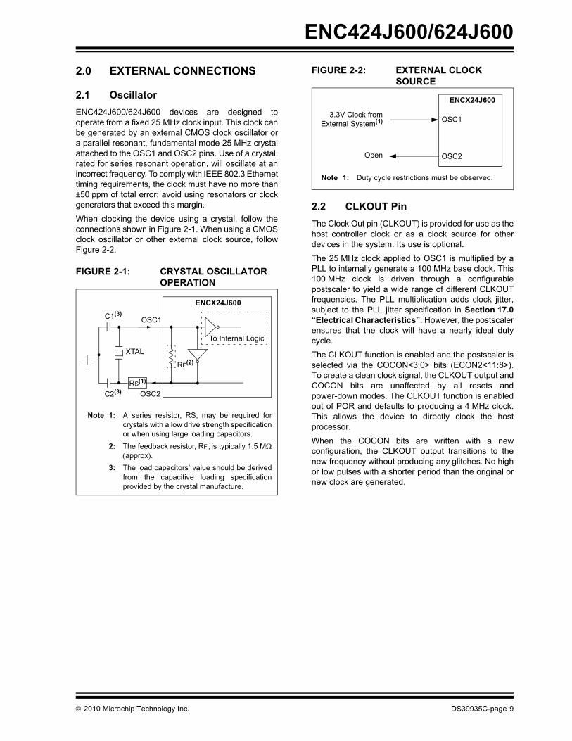
ENC424J600/624J600 devices are designed tooperate from a fixed 25 MHz clock input. This clock canbe generated by an external CMOS clock oscillator ora parallel resonant, fundamental mode 25 MHz crystalattached to the OSC1 and OSC2 pins. Use of a crystal,rated for series resonant operation, will oscillate at anincorrect frequency. To comply with IEEE 802.3 Ethernettiming requirements, the clock must have no more than±50 ppm of total error; avoid using resonators or clockgenerators that exceed this margin.
When clocking the device using a crystal, follow theconnections shown in Figure 2-1. When using a CMOSclock oscillator or other external clock source, followFigure 2-2.
FIGURE 2-1: CRYSTAL OSCILLATOR OPERATION
FIGURE 2-2: EXTERNAL CLOCK SOURCE
2.2 CLKOUT Pin
The Clock Out pin (CLKOUT) is provided for use as thehost controller clock or as a clock source for otherdevices in the system. Its use is optional.
The 25 MHz clock applied to OSC1 is multiplied by aPLL to internally generate a 100 MHz base clock. This100 MHz clock is driven through a configurablepostscaler to yield a wide range of different CLKOUTfrequencies. The PLL multiplication adds clock jitter,subject to the PLL jitter specification in Section 17.0“Electrical Characteristics”. However, the postscalerensures that the clock will have a nearly ideal dutycycle.
The CLKOUT function is enabled and the postscaler isselected via the COCON<3:0> bits (ECON2<11:8>).To create a clean clock signal, the CLKOUT output andCOCON bits are unaffected by all resets andpower-down modes. The CLKOUT function is enabledout of POR and defaults to producing a 4 MHz clock.This allows the device to directly clock the hostprocessor.
When the COCON bits are written with a newconfiguration, the CLKOUT output transitions to thenew frequency without producing any glitches. No highor low pulses with a shorter period than the original ornew clock are generated.
C1(3)
C2(3)
XTAL
OSC2
RS(1)
OSC1
RF(2)
To Internal Logic
Note 1: A series resistor, RS, may be required forcrystals with a low drive strength specificationor when using large loading capacitors.
2: The feedback resistor, RF, is typically 1.5 Mapprox.
3: The load capacitors’ value should be derivedfrom the capacitive loading specificationprovided by the crystal manufacture.
ENCX24J600
3.3V Clock fromExternal System(1) OSC1
OSC2Open
Note 1: Duty cycle restrictions must be observed.
ENCX24J600
2010 Microchip Technology Inc. DS39935C-page 9

ENC424J600/624J600
2.3 Voltage and Bias Pin
2.3.1 VDD AND VSS PINS
To reduce on-die noise levels and provide for thehigh-current demands of Ethernet, there are manypower pins on ENC424J600/624J600 devices:
• VDD and VSS
• VDDOSC and VSSOSC
• VDDPLL and VSSPLL
• VDDRX and VSSRX
• VDDTX and VSSTX
Each VDD and VSS pin pair above should have a 0.1 Fceramic bypass capacitor placed as close to the pins aspossible. For best EMI emission suppression, othersmaller capacitors, such as 0.001 F, should be placedimmediately across VDDTX/VSSTX and VDDPLL/VSSPLL.
All VDD power supply pins must be externally con-nected to the same 3.3V ±10% power source. Similarly,all VSS supply references must be externally connectedto the same ground node. If a ground connectionappears on two pins (e.g., VSSTX), connect both pins;do not allow either to float. In addition, it isrecommended that the exposed bottom metal pad onthe 44-pin QFN package be tied to VSS.
Placing ferrite beads or inductors between any two ofthe supply pins (e.g., between VDDOSC and VDDRX) isnot recommended. However, it is acceptable to isolateall of the VDD supplies from the main circuit power sup-ply through a single ferrite bead or inductor, if desiredfor supply noise suppression reasons. Such isolation isgenerally not necessary.
2.3.2 VCAP PIN
Most of the device’s digital logic operates at a nominal1.8V. This voltage is supplied by an on-chip voltageregulator, which generates the digital supply voltagefrom the VDD rail. The only external componentrequired is an external filter capacitor, connected fromthe VCAP pin to ground, as shown in Figure 2-3. A valueof at least 10 F is recommended.
The capacitor must also have a relatively low Equiva-lent Series Resistance (ESR). It is recommended thata low-ESR capacitor (ceramic, tantalum or similar)should be used and high-ESR capacitors (such asaluminum electrolytic) should be avoided.
The internal regulator is not designed to drive externalloads; therefore, do not attach other circuitry to VCAP.
FIGURE 2-3: VCAP CONNECTIONS
2.3.3 RBIAS PIN
The internal analog circuitry in the PHY modulerequires that an external 12.4 kΩ, 1% resistor beattached from RBIAS to ground, as shown inFigure 2-4. The resistor influences the TPOUT+/-signal amplitude. The RBIAS resistor should be placedas close as possible to the chip with no immediatelyadjacent signal traces in order to prevent noisecapacitively coupling into the pin and affecting thetransmit behavior. It is recommended that the resistorbe a surface mount type.
FIGURE 2-4: RBIAS RESISTOR
VDD
VCAP
VSS
ENCX24J600
10 F
3.3V
0.1 F
Regulator
+3.3V
I/O, PHY
+1.8V
Core, RAM,MAC
RBIAS
ENCX24J600
12.4k1%
PHY
DS39935C-page 10 2010 Microchip Technology Inc.

ENC424J600/624J600
2.4 Ethernet Signal Pins and External Magnetics
Typical applications for ENC424J600/624J600 devicesrequire an Ethernet transformer module, and a fewresistors and capacitors to implement a completeIEEE 802.3 compliant 10/100 Ethernet interface, asshown in Figure 2-5.
The Ethernet transmit interface consists of two pins:TPOUT+ and TPOUT-. These pins implement adifferential pair and a current-mode transmitter. Togenerate an Ethernet waveform, ordinary applicationsrequire the use of a 1:1 center tapped pulsetransformer, rated for 10/100 or 10/100/1000 Ethernetoperations. When the Ethernet module is enabled andlinked with a partner, current is continually sunkthrough both TPOUT pins. When the PHY is activelytransmitting, a differential voltage is created on theEthernet cable by varying the relative current sunk byTPOUT+ compared to TPOUT-.
The Ethernet receive interface similarly consists of adifferential pair: TPIN+ and TPIN-. To meet IEEE 802.3compliance and help protect against electrostatic dis-charge, these pins are normally isolated from theEthernet cable by a 1:1 center tapped transformer(available in the same package as the TX transformer).
Internally, the PHY uses a high-speed ADC to samplethe receive waveform and decodes it using a DSP. ThePHY implements many robustness features, including
baseline wander correction (applicable to 100Base-TX)and automatic RX polarity correction (applicable to10Base-T).
Four 49.9Ω, 1% resistors are required for propertermination of the TX and RX transmission lines. If theboard layout necessitates long traces between theENCX24J600 and Ethernet transformers, the termina-tion resistors should be placed next to the siliconinstead of the transformers.
On the receive signal path, two 6.8 nF 10% capacitorsare used. These capacitors, in combination with the49.9 termination resistors, form an RC high-pass filterto reduce baseline wander. For best performance,these capacitors should not be omitted or changed.The various remaining capacitors provide DC currentblocking and provide stability to the common-modevoltage of both of the differential pairs. The TPIN+/-pins weakly output a common-mode voltage that isacceptable to the internal ADC. For proper operation,do not attempt to externally force the TPIN+/-common-mode voltage to some other value.
The 10Ω 1% resistor provides a current path from thepower supply to the center tap of the TX transformer.As mentioned previously, the TPOUT+/- pinsimplement a Current mode drive topology in which thepins are only capable of sinking current; they do notproduce a direct voltage. This current path through thetransformer generates the transmit waveform. The 10Ωresistor reduces the amount of heat that the PHY wouldhave to dissipate, and therefore, must have a powerrating of 1/12W or better.
FIGURE 2-5: TYPICAL ETHERNET MAGNETICS CONNECTIONS
ENCX24J600
TPOUT+
TPOUT-
TPIN+
TPIN-
3.3V
1
2
3
4
5
6
7
8
RJ-45
1:1 CT
1:1 CT
1000 pF, 2 kV
75 75 75 75
49.9, 1%
49.9, 1%
49.9, 1%
49.9, 1%
0.01 F
0.01 F
1
6.8 nF, 10%
6.8 nF, 10%
10, 1/12W, 1%
2010 Microchip Technology Inc. DS39935C-page 11

ENC424J600/624J600
2.4.1 ADDITIONAL EMI AND LAYOUT CONSIDERATIONS
To reduce EMI emissions, common-mode chokes areshown adjacent to the transformers on the cable(RJ-45) side. These chokes come standard in typicalEthernet transformer modules. Because theENCX24J600 PHY uses a current-mode drive topol-ogy, the transmit choke must normally be located onthe cable side of the transmit transformer. Orienting themagnetics such that the choke is on the PHY side of thetransmit transformer usually results in a distorted,non-compliant transmit waveform. However, somemagnetics which wrap the TX center tap wire aroundthe TX choke core can also be used to generate acompliant waveform (Figure 2-6). These types of trans-formers may be desirable in some Power-over Ethernet(PoE) applications.
FIGURE 2-6: ALTERNATE TX CHOKE TOPOLOGY
The common-mode choke on the RX interface can beplaced on either the cable side or PHY side of thereceive transformer. Recommended and required mag-netics characteristics are located in Section 17.0“Electrical Characteristics”.
The four 75Ω resistors and high-voltage capacitor inFigure 2-5 are intended to prevent each of the twistedpairs in the Ethernet cables from floating and radiatingEMI. Their implementation may require adjustment inPoE applications.
Unless the TX and RX signal pairs are kept short, theyshould be routed between the ENCX24J600 and theEthernet connector following differential routing rules.Like Ethernet cables, 100Ω characteristic impedanceshould be targeted for the differential traces. The use ofvias, which introduce impedance discontinuities,should be minimized. Other board level signals shouldnot run immediately parallel to the TX and RX pairs tominimize capacitive coupling and crosstalk.
2.5 LEDA and LEDB Pins
The LEDA and LEDB pins provide dedicated LEDstatus indicator outputs. The LEDs are intended todisplay link status and TX/RX activity among otherprogrammable options; however, the use of one or bothis entirely optional. The pins are driven automatically bythe hardware and require no support from the hostmicrocontroller. Aside from the LEDs themselves, acurrent-limiting resistor is generally the only requiredcomponent.
By default on POR, LEDA displays the Ethernet linkstatus, while LEDB displays PHY-level TX/RX activity.Because the LEDs operate at the PHY level, RXactivity will be displayed on LEDB any time Ethernetpackets are detected, regardless of if the packet is validand meets the correct RX filtering criteria.
Normally, the device illuminates the LED by sourcingcurrent out of the pin, as shown in Figure 2-7. Connect-ing the LED in reverse, with the anode connected toVDD and the cathode to LEDA/LEDB (through acurrent-limiting resistor), causes the LED to show“inverted sense” behavior, lighting the LED when itshould be off and extinguishing the LED when the LEDshould be on.
FIGURE 2-7: SINGLE COLOR LED CONNECTION
Both LEDs automatically begin operation wheneverpower is applied, a 25 MHz clock is present and theEthernet magnetics are present and wired correctly. Aconnection to the host microcontroller via the SPI orPSP interface is not required. LEDA and LEDB can,therefore, be used as a quick indicator of successfulassembly during initial prototype development.
2.5.1 USING BI-COLOR LEDs
In space constrained applications, it is frequently desir-able to use a single bi-color LED to display multipleoperating parameters. These LEDs are connectedbetween LEDA and LEDB, as shown in Figure 2-8.
FIGURE 2-8: BI-COLOR LED CONNECTION
ENCX24J600 devices include two special hardwaredisplay modes to make maximal use of a bi-color LED.These modes are selected when the LACFG<3:0> andLBCFG<3:0> bits (EIDLED<15:8>) are set to ‘1111’ or‘1110’. In these configurations, the link state turns theLED on, the speed/duplex state sets the LED color andTX/RX events cause the LED to blink off. If a link ispresent, no TX/RX events are occurring and thespeed/duplex state is 100 Mbps/full duplex,respectively, then the LEDB pin will be driven high whileLEDA will be driven low.
1:1 CT
PHY RJ-45
180LEDAorLEDB LED
180LEDA
LEDB
LEDBi-Color
DS39935C-page 12 2010 Microchip Technology Inc.

ENC424J600/624J600
2.6 INT Pin
The INT pin is an active-low signal that is used to flaginterrupt events to external devices. Depending on theapplication, it can be used to signal the host micro-controller whenever a packet has been received ortransmitted, or that some other asynchronousoperation has occurred. It can also be used to wake-upthe microcontroller or other system components basedon LAN activity; its use is optional.
The INT pin is driven high when no interrupt is pendingand is driven low when an interrupt has occurred. Itdoes not go into a high-impedance state, except duringinitial power-on while the multiplexed SPISEL pinfunction is being used.
Since ENC424J600/624J600 devices incorporate abuffer for storing transmit and receive packets, the hostmicrocontroller never needs to perform real-timeoperations on the device. The microcontroller can pollthe device registers to discover if the device status haschanged.
2.7 Host Interface Pins
For the maximum degree of flexibility in interfacing withmicrocontrollers, ENC424J600/624J600 devices offera choice between a serial interface based on the SerialPeripheral Interface (SPI) standard, and a flexible 8 or16-bit parallel slave port (PSP) interface. Only oneinterface may be used at any given time.
The I/O interface is hardware selected on power-upusing the SPISEL function on the INT/SPISEL pin. Thisis done by latching in the voltage level applied to the pin
approximately 1 to 10 s after power is applied to thedevice and the device exits Power-on Reset. If SPISELis latched at a logic high state, the serial interface isenabled. If SPISEL is latched at a logic low state, thePSP interface is enabled. Figure 2-9 shows exampleconnections required to select the SPI or PSP interfaceupon power-up.
To ensure the SPI interface is selected upon power-up,an external pull-up resistor to VDD must be connectedto the SPISEL pin. Alternatively, if the parallel interfaceis to be used, a pull-down resistor to VSS must beconnected to the SPISEL pin. In most circuits, it is rec-ommended that a 100 kΩ or smaller resistor be used toensure that the correct logic level is latched in reliably.If a large capacitance is present in the SPISEL circuit,such as from stray capacitance, a smaller pull-up orpull-down resistor may be required to compensate andensure the correct level is sensed during power-up.
As SPISEL is multiplexed with the INT interrupt outputfunction, a direct connection to VDD or VSS without aresistor is prohibited. If INT is connected to the hostmicrocontroller, the microcontroller must leave thissignal in a high-impedance state and not attempt todrive it to an incorrect logic state during power-up.
If the VDD supply has a slow ramp rate, the device willexit POR, exceed the 1 to 10 s latch timer and samplethe SPISEL pin state before VDD has reached the spec-ified minimum operating voltage of the device. In thiscase, the device will still latch in the correct value,assuming the minimum VIH (D004) or maximum VIL
(D006) specification is met, which is a function of VDD.
FIGURE 2-9: USING THE INT/SPISEL PIN TO SELECT THE I/O INTERFACE
I/O
SCK
SDO
SDI
INT0
MCU
CS
SCK
SI
SO
INT/SPISEL
ENCX24J6003.3V
100kPMALL
PMCS2
RMRD
PMWR
INT0
MCU
AL
CS
RD
WR
INT/SPISEL
ENCX24J600
ADxPMAx/PMDx
100k
SPI Selected PSP Selected (Mode 5 shown)
~2.2V
VSS
(internal weak pull-up on CS enabled) (internal weak pull-down on CS enabled)
2010 Microchip Technology Inc. DS39935C-page 13

ENC424J600/624J600
2.7.1 SPI
When enabled, the SPI interface is implemented withfour pins:
• CS
• SO
• SI
• SCK
All four of these pins must be connected to use the SPIinterface.
The CS, SI and SCK input pins are 5V tolerant. The SOpin is also 5V tolerant when in a high-impedance state.SO is always high-impedance when CS is connected tologic high (i.e., chip not selected).
When the SPI interface is enabled, all PSP interfacepins (except PSPCFG2 and PSPCFG3 onENC624J600 devices) are unused. They are placed ina high-impedance state and their input buffers are dis-abled. For best ESD performance, it is recommendedthat the unused PSP pins be tied to either VSS or VDD.However, these pins may be left floating if it is desirablefor board level layout and routing reasons.
When using an ENC624J600 device in SPI mode, it isrecommended that the PSPCFG2 and PSPCFG3 pinsbe tied to either VSS or any logic high voltage, and notbe left floating. The particular state used is unimportant.
2.7.2 PSP
Depending on the particular device, the PSP interfaceis implemented with up to 34 pins. The interface ishighly configurable to accommodate many different
parallel interfaces; not all available pins are used inevery configuration. Up to 8 different operating modesare available. These are explained in detail inSection 5.0 “Parallel Slave Port Interface (PSP)”.
The PSPCFG pins control which parallel interfacemode is used. The values on these pins are latchedupon device power-up in the same manner as theSPISEL pin. The combinations of VDD and VSS volt-ages on the different PSPCFG mode pins determinethe PSP mode according to Table 2-1.
On ENC424J600 devices, only PSP Modes 5 and 6(8-bit width, multiplexed data and address) areavailable. The mode is selected by applying VSS orVDD, respectively, to PSPCFG0.
On ENC624J600 devices, all eight PSP modes areavailable and are selected by connecting thePSPCFG<4:1> pins directly to VDD or ground. Themode selection is encoded such that the multiplexedpin functions, AD14 (on PSPCFG1) and SCK/AL (onPSPCFG4), are used only in the “don’t care” positions.Therefore, pull-up/pull-down resistors are not requiredfor these pins.
All PSP pins, except for AD<15:0>, are inputs to theENC624J600 family device and are 5V tolerant. TheAD<15:0> pins are bidirectional I/Os and are 5Vtolerant in Input mode. The pins are always inputswhen the CS signal is low (chip not selected).
Any unused PSP pins are placed in a high-impedancestate. However, it is recommended that they be tied toeither Vss or a logic high voltage and not be left floating.
TABLE 2-1: PSP MODE SELECTION FOR ENC424J600/624J600 DEVICES
Interface Mode
INT/SPISEL
PSPCFG
Pins Used
0 1 2 3 4
44-Pin
PSP Mode 5 Pull Down 0 — — — — AL, CS, RD, WR, AD<14:0>
PSP Mode 6 Pull Down 1 — — — — AL, CS, RW, EN, AD<14:0>
64-Pin
PSP Mode 1 Pull Down — x 0 0 0 CS, RD, WR, A14:A0, AD<7:0>
PSP Mode 2 Pull Down — x 0 0 1 CS, RW, EN, A14:A0, AD<7:0>
PSP Mode 3 Pull Down — x 1 0 0 CS, RD, WRL, WRH, A<13:0>, AD<15:0>
PSP Mode 4 Pull Down — x 1 0 1 CS, RW, B0SEL, B1SEL, A<13:0>, AD<15:0>
PSP Mode 5 Pull Down — 0 0 1 x AL, CS, RD, WR, AD<14:0>
PSP Mode 6 Pull Down — 1 0 1 x AL, CS, RW, EN, AD<14:0>
PSP Mode 9 Pull Down — 0 1 1 x AL, CS, RD, WRL, WRH, AD<15:0>
PSP Mode 10 Pull Down — 1 1 1 x AL, CS, RW, B0SEL, B1SEL, AD<15:0>
Legend: x = don’t care, 0 = logic low (tied to VSS), 1 = logic high (tied to VDD), — = pin not present
DS39935C-page 14 2010 Microchip Technology Inc.

ENC424J600/624J600
2.7.3 CS/CS PIN
The chip select functions for the serial and parallelinterfaces are shared on one common pin, CS/CS. Thispin is equipped with both internal weak pull-up andweak pull-down resistors. If the SPI interface isselected (CS), the pull-up resistor is automaticallyenabled and the pull-down resistor is disabled. If thePSP interface is chosen (CS), the pull-down resistor isautomatically enabled and the pull-up resistor isdisabled. This allows the CS/CS pin to stay in theunselected state when not being driven, avoiding theneed for an external board level resistor on this pin.
When enabled by using SPI mode, the internal weakpull-up only pulls the CS/CS pin up to approximatelyVDD-1.1V or around 2.2V at typical conditions withoutany loading; it does not pull all the way to VDD. Whenusing the PSP interface, the pull-down will be enabled,which is capable of pulling all the way to VSS whenunloaded.
2.8 Digital I/O Levels
All digital output pins on ENC424J600/624J600devices contain CMOS output drivers that are capableof sinking and sourcing up to 18 mA continuously. Alldigital inputs and I/O pins operating as inputs are 5Vtolerant. These features generally mean that theENCX24J600 can connect directly to the hostmicrocontroller without the need of any glue logic.However, some consideration may be necessary wheninterfacing with 5V systems.
Since the digital outputs drive only up to the VDD
voltage (3.3V nominally), the voltage may not be highenough to ensure a logical high is detected by 5Vsystems which have high input thresholds. In suchcases, unidirectional level translation from the 3.3VENCX24J600 up to the 5V host microcontroller may beneeded.
When using the SPI interface, an economical 74HCT08(quad AND gate), 74ACT125 (quad 3-state buffer) orother 5V CMOS chip with TTL level input buffers maybe used to provide the necessary level shifting. Theuse of 3-state buffers permits easy integration intosystems which share the SPI bus with other devices.However, users must make certain that the propaga-tion delay of the level translator does not reduce themaximum SPI frequency below desired levels.Figure 2-10 and Figure 2-11 show two exampletranslation schemes.
When using the PSP interface, eight, or all sixteen ofthe ADx pins, may need level translation when perform-ing read operations on the ENCX24J600. The 8-bit74ACT245 or 16-bit 74ACT16245 bus transceiver, orsimilar devices, may be useful in these situations.
FIGURE 2-10: LEVEL SHIFTING ON THE SPI INTERFACE USING AND GATES
FIGURE 2-11: LEVEL SHIFTING ON THE SPI INTERFACE USING 3-STATE BUFFERS
I/O
SCK
SDO
SDI
INTx
MCU
CS
SCK
SI
SO
INT/SPISEL
ENCX24J600
CLKOUTOSC1
3.3V
100k
I/O
SCK
SDO
SDI
INTx
MCU
CS
SCK
SI
SO
INT/SPISEL
ENCX24J600
CLKOUTOSC1
3.3V
100k
2010 Microchip Technology Inc. DS39935C-page 15

ENC424J600/624J600
NOTES:
DS39935C-page 16 2010 Microchip Technology Inc.

ENC424J600/624J600
3.0 MEMORY ORGANIZATIONAll memory in ENC424J600/624J600 devices isimplemented as volatile RAM. Functionally, there arefour unique memories:
• Special Function Registers (SFRs)• PHY Special Function Registers• Cryptographic Data Memory• SRAM Buffer
The SFRs configure, control and provide statusinformation for most of the device. They are directlyaccessible through the I/O interface.
The PHY SFRs configure, control and provide statusinformation for the PHY module. They are locatedinside the PHY module and isolated from all othernormal SFRs, so they are not directly accessiblethrough the I/O interface.
The cryptography data memory is used to store keyand data material for the modular exponentiation, AESand MD5/SHA-1 hashing engines. This memory areacan only be accessed through the DMA module.
The SRAM buffer is a bulk 12K x 16-bit (24 Kbyte) RAMarray used for TX and RX packet buffering, as well asgeneral purpose storage by the host microcontroller.Although the SRAM uses a 16-bit word, it isbyte-writable. This memory is indirectly accessiblethrough pointers on all I/O interfaces. It can also beaccessed directly through the PSP interfaces.
3.1 I/O Interface and Memory Map
Depending on the I/O interface selected, the fourmemories are arranged into two or three different memoryaddress spaces. When the serial interface is selected, thememories are grouped into three address spaces. Whenone of the parallel interfaces is selected, they arearranged into two address spaces. In all cases, the PHYSFRs reside in their own memory address space.
3.1.1 SPI INTERFACE MAP
When the SPI interface is selected, the device memorymap is comprised of three memory address spaces(Figure ):
• the SFR area• the main memory area• the PHY register area
The SFR area is directly accessible to the user. This isa linear memory space that is 160 bytes long. Forefficiency, the SFR area can be addressed as fourbanks of 32 bytes each, starting at the beginning of thespace (00h), with an additional unbanked area of32 bytes at the end of the SFR memory. Bankedaddressing allows SFRs to be addressed with feweraddress bits being exchanged over the serial interfacefor each transaction. This decreases protocol overheadand enhances performance. SFRs can also be directlyaddressed by their 8-bit unbanked addresses usingunbanked SPI commands. This allows for a simplerinterface whenever transaction overhead is not critical.
The main memory area is organized as a linear,byte-addressable space of 32 Kbytes. Of this, the first24-Kbyte area (0000h through 5FFFh) is implementedas the SRAM buffer. The buffer is accessed by thedevice using several SFRs as memory pointers andvirtual data window registers, as described inSection 3.5.5 “Indirect SRAM Buffer Access”.
Addresses in the main memory area, between 7800hand 7C4Fh, are mapped to the memory for the crypto-graphic data modules. These addresses are notdirectly accessible through the SPI interface; they canonly be accessed through the DMA.
The PHY SFRs are the final memory space. This is alinear, word-addressable memory space of 32 words.This area is only accessible by the MIIM interface (seeSection 3.3 “PHY Special Function Registers” formore details).
FIGURE 3-1: ENC424J600/624J600 MEMORY MAP WITH SPI INTERFACE
0000h
5FFFh
00h
SRAM Buffer
Unimplemented
7800h
7C4Fh
Bank 0
Bank 1
Bank 2
Bank 3
Unbanked(inaccessible using banked opcodes)
1Fh20h
3Fh40h
5Fh60h
7Fh80h
9Fh
00h
1Fh00h
1Fh00h
1Fh00h
1Fh
Cryptographic Data(DMA access only)
Unimplemented7FFFh16-Bit, MIIM Access Only
00h
1Fh
PHY Register MIREGADR
Banked OpcodesUnbanked Opcodes PointersSFR Area
Main Area
Area
2010 Microchip Technology Inc. DS39935C-page 17

ENC424J600/624J600
3.1.2 PSP INTERFACE MAPS
When one of the parallel interfaces is selected, thememory map is very different from the SPI map. Thereare two different memory address spaces (Figure 3-2):
• the main memory area• the PHY register area
As in the serial memory map, the main memory area isa linear, byte-addressable space of 32 Kbytes, with theSRAM buffer located in the first 24-Kbyte region. Thecryptographic data memory is also mapped to the samelocation as in the serial memory map. The main differ-ence is that the SFRs are now located to an area with ahigher address than the cryptographic data space. Addi-tional memory areas above the SFRs are reserved fortheir accompanying Bit Set and Bit Clear registers.
Except for the cryptographic data memory, alladdresses in the main memory area are directlyaccessible using the PSP bus. As with the serial inter-face, the cryptographic memory can only be accessedthrough the DMA.
The difference between the 8-bit and 16-bit interfaces ishow the SRAM buffer is addressed by the externaladdress bus. In 16-bit data modes, the address bustreats the buffer as a 16-byte wide, word-addressablespace, spanning 000h to 3FFFh. In 8-bit data modes, theaddress bus treats the buffer as an 8-bit, byte-address-able space, ranging from 0000h to 7FFFh. In either case,the SFRs used as memory pointers still address thebuffer as a byte-wide, byte-addressable space.
The PHY SFR space is implemented in the samemanner as the SPI interface described above.
In both 8-bit and 16-bit PSP modes, full device func-tionality can be realized without using the full width ofthe address bus. This is because the SRAM buffer canstill be read and written to by using SFR pointers. Inpractical terms, this can allow designers in space or pinconstrained applications to only connect a subset of theA or AD address pins to the host microcontroller. Forexample, in the 8-Bit Multiplexed PSP Modes 5 or 6,tying pins, AD<14:9> to VDD, still allows direct addressaccess to all SFRs. This reduces the number of pinsrequired for connection to the host controller, includingthe interface control pins to 12 or 13.
FIGURE 3-2: ENC424J600/624J600 MEMORY MAPS FOR PSP INTERFACES(1)
0000h
2FFFh
SRAM Buffer
Unimplemented
Cryptographic Data(DMA access only)
3F00h
Unimplemented
Special Function Registers (R/W)3F4Fh
0000h
5FFFh
7800h(2)
7C4Fh(2)
PSP Address Bus (Word Address)Pointers (Byte Address)
16-Bit, MIIM Access Only00h
1Fh
PHY Register AreaMIREGADR
3F80hSFR Bit Set Registers
3FBFh3FC0h
SFR Bit Clear Registers3FFFh
16-Bit, MIIM Access Only00h
1Fh
PHY Register AreaMIREGADR
0000h
5FFFh
SRAM Buffer
Unimplemented
7800h(2)
7C4Fh(2)
Cryptographic Data(DMA access only)
7E00h
Unimplemented
Special Function Registers (R/W) 7E9Fh
PSP Address Bus and All Pointers
7F00hSFR Bit Set Registers 7F7Fh
7F80hSFR Bit Clear Registers
7FFFh
Main Area Main Area8-Bit PSP 16-Bit PSP
Note 1: Memory areas not shown to scale.2: Addresses in this range are accessible only through internal address pointers of the DMA module.
DS39935C-page 18 2010 Microchip Technology Inc.

ENC424J600/624J600
3.2 Special Function Registers
The SFRs provide the main interface between the hostcontroller and the on-chip Ethernet controller logic.Writing to these registers controls the operation of theinterface, while reading the registers allows the hostcontroller to monitor operations.
All registers are 16 bits wide. On the SPI and 8-bit PSPinterfaces, which are inherently byte-oriented, theregisters are split into separate high and low locationswhich are designated by an “H” or “L” suffix, respec-tively. All registers are organized in little-endian formatsuch that the low byte is always at the lower memoryaddress.
Some of the available addresses are unimplemented ormarked as reserved. These locations should not bewritten to. Data read from reserved locations should beignored. Reading from unimplemented locations willreturn ‘0’. When reading and writing to registers whichcontain reserved bits, any rules stated in the registerdefinition should be observed.
The addresses of all user-accessible registers areprovided in Tables 3-1 through 3-6. A complete bit levellisting of the SFRs is presented in Table 3-7 (page 26).
3.2.1 E REGISTERS
SFRs with names starting with “E” are the primarycontrol and pointer registers. They configure and con-trol all of the (non-MAC) top-level features of thedevice, as well as manipulate the pointers that definethe memory buffers. These registers can be read andwritten in any order, with any length, without concernfor address alignment.
3.2.2 MAC REGISTERS
SFRs with names that start with “MA” or “MI” areimplemented in the MAC module hardware. For thisreason, their operation differs from “E” registers in twoways.
First, MAC registers support read and write operationsonly. Individual bit set and bit clear operations cannotbe performed.
Additionally, MAC registers must always be written asa 16-bit word, regardless of the I/O interface beingused. That is, on the SPI or 8-bit PSP interfaces, allwrite operations must be performed by writing to thelow byte, followed by a write to the associated highbyte. On 16-bit PSP interfaces, both write enables orbyte selects must be asserted to perform the 16-bitwrite. Non-sequential writes, such as writing to the lowbyte of one MAC register, the low byte of a secondMAC register and then the high byte of the first registercannot be performed.
3.2.3 SPI REGISTER MAP
As previously described, the SFR memory ispartitioned into four banks plus a special region that isnot bank addressable. Each bank is 32 bytes long andaddressed by a 5-bit address value. All SFR memorymay also be accessed via unbanked SPI opcodeswhich use a full 8-bit address to form a linear addressmap without banking.
The last 10 bytes (16h to 1Fh) of all SPI banks point toa common set of five registers: EUDAST, EUDAND,ESTAT, EIR and ECON1. These are key registers usedin controlling and monitoring the operation of thedevice. Their common banked addresses allow easyaccess without switching the bank.
The SPI interface implements a comprehensiveinstruction set that allows for reading and writing ofregisters, as well as setting and clearing individual bitsor bit fields within registers. The SPI instruction set isexplained in detail in Section 4.0 “Serial PeripheralInterface (SPI)”.
The SFR map for the SPI interface is shown inTable 3-1. Registers are presented by a bank. Thebanked (5-bit) address applicable to the registers ineach row is shown in the left most column. Theunbanked (8-bit) address for each register is shown tothe immediate left of the register name.
Note: SFRs in the unbanked region (80h through9Fh) cannot be accessed using bankedaddressing. The use of an unbanked SFRopcode is required to perform operationson these registers.
2010 Microchip Technology Inc. DS39935C-page 19

ENC424J600/624J600
TABLE 3-1: ENC424J600/624J600 SFR MAP (SPI INTERFACE)B
an
ke
d R
eg
iste
r A
dd
res
se
sBank 0
(00h offset)Bank 1
(20h offset)Bank 2
(40h offset)Bank 3
(60h offset)Unbanked(1)
(80h offset)U
nb
an
ke
d
Ad
dre
ss
Name
Un
ba
nk
ed
A
dd
res
s
Name
Un
ba
nk
ed
A
dd
res
s
Name
Un
ba
nk
ed
A
dd
res
s
Name
Un
ba
nk
ed
A
dd
res
s
Name
00 00 ETXSTL 20 EHT1L 40 MACON1L 60 MAADR3L 80 EGPDATA(2)
01 01 ETXSTH 21 EHT1H 41 MACON1H 61 MAADR3H 81 Reserved
02 02 ETXLENL 22 EHT2L 42 MACON2L 62 MAADR2L 82 ERXDATA(2)
03 03 ETXLENH 23 EHT2H 43 MACON2H 63 MAADR2H 83 Reserved
04 04 ERXSTL 24 EHT3L 44 MABBIPGL 64 MAADR1L 84 EUDADATA(2)
05 05 ERXSTH 25 EHT3H 45 MABBIPGH 65 MAADR1H 85 Reserved
06 06 ERXTAILL 26 EHT4L 46 MAIPGL 66 MIWRL 86 EGPRDPTL
07 07 ERXTAILH 27 EHT4H 47 MAIPGH 67 MIWRH 87 EGPRDPTH
08 08 ERXHEADL 28 EPMM1L 48 MACLCONL 68 MIRDL 88 EGPWRPTL
09 09 ERXHEADH 29 EPMM1H 49 MACLCONH 69 MIRDH 89 EGPWRPTH
0A 0A EDMASTL 2A EPMM2L 4A MAMXFLL 6A MISTATL 8A ERXRDPTL
0B 0B EDMASTH 2B EPMM2H 4B MAMXFLH 6B MISTATH 8B ERXRDPTH
0C 0C EDMALENL 2C EPMM3L 4C Reserved 6C EPAUSL 8C ERXWRPTL
0D 0D EDMALENH 2D EPMM3H 4D Reserved 6D EPAUSH 8D ERXWRPTH
0E 0E EDMADSTL 2E EPMM4L 4E Reserved 6E ECON2L 8E EUDARDPTL
0F 0F EDMADSTH 2F EPMM4H 4F Reserved 6F ECON2H 8F EUDARDPTH
10 10 EDMACSL 30 EPMCSL 50 Reserved 70 ERXWML 90 EUDAWRPTL
11 11 EDMACSH 31 EPMCSH 51 Reserved 71 ERXWMH 91 EUDAWRPTH
12 12 ETXSTATL 32 EPMOL 52 MICMDL 72 EIEL 92 Reserved
13 13 ETXSTATH 33 EPMOH 53 MICMDH 73 EIEH 93 Reserved
14 14 ETXWIREL 34 ERXFCONL 54 MIREGADRL 74 EIDLEDL 94 Reserved
15 15 ETXWIREH 35 ERXFCONH 55 MIREGADRH 75 EIDLEDH 95 Reserved
16 16 EUDASTL 36 EUDASTL 56 EUDASTL 76 EUDASTL 96 Reserved
17 17 EUDASTH 37 EUDASTH 57 EUDASTH 77 EUDASTH 97 Reserved
18 18 EUDANDL 38 EUDANDL 58 EUDANDL 78 EUDANDL 98 Reserved
19 19 EUDANDH 39 EUDANDH 59 EUDANDH 79 EUDANDH 99 Reserved
1A 1A ESTATL 3A ESTATL 5A ESTATL 7A ESTATL 9A Reserved
1B 1B ESTATH 3B ESTATH 5B ESTATH 7B ESTATH 9B Reserved
1C 1C EIRL 3C EIRL 5C EIRL 7C EIRL 9C Reserved
1D 1D EIRH 3D EIRH 5D EIRH 7D EIRH 9D Reserved
1E 1E ECON1L 3E ECON1L 5E ECON1L 7E ECON1L 9E —
1F 1F ECON1H 3F ECON1H 5F ECON1H 7F ECON1H 9F —
Note 1: Unbanked SFRs can be accessed only by unbanked SPI opcodes.2: When using these registers to access the SRAM buffer, use only the N-byte SRAM instructions. See Section 4.6.2
“Unbanked SFR Operations” and Section 4.6.3 “SRAM Buffer Operations” for more details.
DS39935C-page 20 2010 Microchip Technology Inc.

ENC424J600/624J600
3.2.4 PSP REGISTER MAP
When using a PSP interface, the SFR memory is linear;all registers are directly accessible without banking. Tomaintain consistency with the SPI interface, theEUDAST, EUDAND, ESTAT, EIR and ECON1 registersare instantiated in four locations in the PSP memorymaps. Users may opt to use any one of these fourlocations.
The SFR maps for the 8-bit and 16-bit PSP interfacesare shown in Table 3-2 and Table 3-3, respectively.
TABLE 3-2: ENC424J600/624J600 SFR MAP (BASE REGISTER MAP, 8-BIT PSP INTERFACE)
Addr Name Addr Name Addr Name Addr Name Addr Name
7E00 ETXSTL 7E20 EHT1L 7E40 MACON1L 7E60 MAADR3L 7E80 EGPDATA
7E01 ETXSTH 7E21 EHT1H 7E41 MACON1H 7E61 MAADR3H 7E81 Reserved
7E02 ETXLENL 7E22 EHT2L 7E42 MACON2L 7E62 MAADR2L 7E82 ERXDATA
7E03 ETXLENH 7E23 EHT2H 7E43 MACON2H 7E63 MAADR2H 7E83 Reserved
7E04 ERXSTL 7E24 EHT3L 7E44 MABBIPGL 7E64 MAADR1L 7E84 EUDADATA
7E05 ERXSTH 7E25 EHT3H 7E45 MABBIPGH 7E65 MAADR1H 7E85 Reserved
7E06 ERXTAILL 7E26 EHT4L 7E46 MAIPGL 7E66 MIWRL 7E86 EGPRDPTL
7E07 ERXTAILH 7E27 EHT4H 7E47 MAIPGH 7E67 MIWRH 7E87 EGPRDPTH
7E08 ERXHEADL 7E28 EPMM1L 7E48 MACLCONL 7E68 MIRDL 7E88 EGPWRPTL
7E09 ERXHEADH 7E29 EPMM1H 7E49 MACLCONH 7E69 MIRDH 7E89 EGPWRPTH
7E0A EDMASTL 7E2A EPMM2L 7E4A MAMXFLL 7E6A MISTATL 7E8A ERXRDPTL
7E0B EDMASTH 7E2B EPMM2H 7E4B MAMXFLH 7E6B MISTATH 7E8B ERXRDPTH
7E0C EDMALENL 7E2C EPMM3L 7E4C Reserved 7E6C EPAUSL 7E8C ERXWRPTL
7E0D EDMALENH 7E2D EPMM3H 7E4D Reserved 7E6D EPAUSH 7E8D ERXWRPTH
7E0E EDMADSTL 7E2E EPMM4L 7E4E Reserved 7E6E ECON2L 7E8E EUDARDPTL
7E0F EDMADSTH 7E2F EPMM4H 7E4F Reserved 7E6F ECON2H 7E8F EUDARDPTH
7E10 EDMACSL 7E30 EPMCSL 7E50 Reserved 7E70 ERXWML 7E90 EUDAWRPTL
7E11 EDMACSH 7E31 EPMCSH 7E51 Reserved 7E71 ERXWMH 7E91 EUDAWRPTH
7E12 ETXSTATL 7E32 EPMOL 7E52 MICMDL 7E72 EIEL 7E92 Reserved
7E13 ETXSTATH 7E33 EPMOH 7E53 MICMDH 7E73 EIEH 7E93 Reserved
7E14 ETXWIREL 7E34 ERXFCONL 7E54 MIREGADRL 7E74 EIDLEDL 7E94 Reserved
7E15 ETXWIREH 7E35 ERXFCONH 7E55 MIREGADRH 7E75 EIDLEDH 7E95 Reserved
7E16 EUDASTL 7E36 EUDASTL 7E56 EUDASTL 7E76 EUDASTL 7E96 Reserved
7E17 EUDASTH 7E37 EUDASTH 7E57 EUDASTH 7E77 EUDASTH 7E97 Reserved
7E18 EUDANDL 7E38 EUDANDL 7E58 EUDANDL 7E78 EUDANDL 7E98 Reserved
7E19 EUDANDH 7E39 EUDANDH 7E59 EUDANDH 7E79 EUDANDH 7E99 Reserved
7E1A ESTATL 7E3A ESTATL 7E5A ESTATL 7E7A ESTATL 7E9A Reserved
7E1B ESTATH 7E3B ESTATH 7E5B ESTATH 7E7B ESTATH 7E9B Reserved
7E1C EIRL 7E3C EIRL 7E5C EIRL 7E7C EIRL 7E9C Reserved
7E1D EIRH 7E3D EIRH 7E5D EIRH 7E7D EIRH 7E9D Reserved
7E1E ECON1L 7E3E ECON1L 7E5E ECON1L 7E7E ECON1L 7E9E —
7E1F ECON1H 7E3F ECON1H 7E5F ECON1H 7E7F ECON1H 7E9F —
2010 Microchip Technology Inc. DS39935C-page 21

ENC424J600/624J600
TABLE 3-3: ENC424J600/624J600 SFR MAP (BASE REGISTER MAP, 16-BIT PSP INTERFACE)
3.2.4.1 PSP Bit Set and Bit Clear Registers
A major difference between the SPI and PSP memorymaps is the inclusion of companion Bit Set and BitClear registers for many of the E registers. Since thePSP interface allows direct access to memorylocations, without a command interpreter, there are noinstructions implemented to perform single bitmanipulations. Instead, this interface implementsseparate Bit Set and Bit Clear registers, allowing usersto individually work with volatile bits (such as interruptflags) without the risk of disturbing the values of otherbits. Setting the bit(s) in one of these registers sets orclears the corresponding bit(s) in the base register.
In the PSP interface, Bit Set and Bit Clear registers arelocated in different areas of the addressable memoryspace from their corresponding “base” SFRs. Theaddress of the registers is always at a fixed offset fromtheir corresponding base register. For the 8-bit interface,the offset is 100h (Set) or 180h (Clear). For the 16-bitinterface, the offset is 80H (Set) or C0 (Clear).Symbolically, the names of the companion registers arethe names of the base registers, plus the suffix form“-SET” (or “-SETH/SETL”) for Bit Set registers and“-CLR” (“-CLRH/CLRL”) for Bit Clear registers.
Most SFRs have their own pair of Bit Set and Bit Clearregisters. However, these SFRs do not:
• MAC registers, including MI registers for PHY access
• Read-only status registers (ERXHEAD, ETXSTAT, ETXWIRE and ESTAT)
• All of the SRAM Buffer Pointers and data windows (SFRs located at 7E80h to 7E9Fh in the 8-bit interface, or 3F40h to 3F4Fh in the 16-bit interface)
The Bit Set and Bit Clear registers for the 8-bit PSPinterface are listed in Table 3-4 and Table 3-5,respectively. The registers for the 16-bit interface arelisted together in Table 3-6.
Addr Name Addr Name Addr Name Addr Name Addr Name
3F00 ETXST 3F10 EHT1 3F20 MACON1 3F30 MAADR3 3F40 EGPDATA
3F01 ETXLEN 3F11 EHT2 3F21 MACON2 3F31 MAADR2 3F41 ERXDATA
3F02 ERXST 3F12 EHT3 3F22 MABBIPG 3F32 MAADR1 3F42 EUDADATA
3F03 ERXTAIL 3F13 EHT4 3F23 MAIPG 3F33 MIWR 3F43 EGPRDPT
3F04 ERXHEAD 3F14 EPMM1 3F24 MACLCON 3F34 MIRD 3F44 EGPWRPT
3F05 EDMAST 3F15 EPMM2 3F25 MAMXFL 3F35 MISTAT 3F45 ERXRDPT
3F06 EDMALEN 3F16 EPMM3 3F26 Reserved 3F36 EPAUS 3F46 ERXWRPT
3F07 EDMADST 3F17 EPMM4 3F27 Reserved 3F37 ECON2 3F47 EUDARDPT
3F08 EDMACS 3F18 EPMCS 3F28 Reserved 3F38 ERXWM 3F48 EUDAWRPT
3F09 ETXSTAT 3F19 EPMO 3F29 MICMD 3F39 EIE 3F49 Reserved
3F0A ETXWIRE 3F1A ERXFCON 3F2A MIREGADR 3F3A EIDLED 3F4A Reserved
3F0B EUDAST 3F1B EUDAST 3F2B EUDAST 3F3B EUDAST 3F4B Reserved
3F0C EUDAND 3F1C EUDAND 3F2C EUDAND 3F3C EUDAND 3F4C Reserved
3F0D ESTAT 3F1D ESTAT 3F2D ESTAT 3F3D ESTAT 3F4D Reserved
3F0E EIR 3F1E EIR 3F2E EIR 3F3E EIR 3F4E Reserved
3F0F ECON1 3F1F ECON1 3F2F ECON1 3F3F ECON1 3F4F —
DS39935C-page 22 2010 Microchip Technology Inc.

ENC424J600/624J600
TABLE 3-4: ENC424J600/624J600 SFR MAP (SET REGISTER MAP, 8-BIT PSP INTERFACE)
Bit Set Registers (7F00h to 7F7Fh)(1)
Addr Name Addr Name Addr Name Addr Name
7F00 ETXSTSETL 7F20 EHT1SETL 7F40 Reserved 7F60 Reserved
7F01 ETXSTSETH 7F21 EHT1SETH 7F41 Reserved 7F61 Reserved
7F02 ETXLENSETL 7F22 EHT2SETL 7F42 Reserved 7F62 Reserved
7F03 ETXLENSETH 7F23 EHT2SETH 7F43 Reserved 7F63 Reserved
7F04 ERXSTSETL 7F24 EHT3SETL 7F44 Reserved 7F64 Reserved
7F05 ERXSTSETH 7F25 EHT3SETH 7F45 Reserved 7F65 Reserved
7F06 ERXTAILSETL 7F26 EHT4SETL 7F46 Reserved 7F66 Reserved
7F07 ERXTAILSETH 7F27 EHT4SETH 7F47 Reserved 7F67 Reserved
7F08 — 7F28 EPMM1SETL 7F48 Reserved 7F68 Reserved
7F09 — 7F29 EPMM1SETH 7F49 Reserved 7F69 Reserved
7F0A EDMASTSETL 7F2A EPMM2SETL 7F4A Reserved 7F6A Reserved
7F0B EDMASTSETH 7F2B EPMM2SETH 7F4B Reserved 7F6B Reserved
7F0C EDMALENSETL 7F2C EPMM3SETL 7F4C Reserved 7F6C EPAUSSETL
7F0D EDMALENSETH 7F2D EPMM3SETH 7F4D Reserved 7F6D EPAUSSETH
7F0E EDMADSTSETL 7F2E EPMM4SETL 7F4E Reserved 7F6E ECON2SETL
7F0F EDMADSTSETH 7F2F EPMM4SETH 7F4F Reserved 7F6F ECON2SETH
7F10 EDMACSSETL 7F30 EPMCSSETL 7F50 Reserved 7F70 ERXWMSETL
7F11 EDMACSSETH 7F31 EPMCSSETH 7F51 Reserved 7F71 ERXWMSETH
7F12 — 7F32 EPMOSETL 7F52 Reserved 7F72 EIESETL
7F13 — 7F33 EPMOSETH 7F53 Reserved 7F73 EIESETH
7F14 — 7F34 ERXFCONSETL 7F54 Reserved 7F74 EIDLEDSETL
7F15 — 7F35 ERXFCONSETH 7F55 Reserved 7F75 EIDLEDSETH
7F16 EUDASTSETL 7F36 EUDASTSETL 7F56 EUDASTSETL 7F76 EUDASTSETL
7F17 EUDASTSETH 7F37 EUDASTSETH 7F57 EUDASTSETH 7F77 EUDASTSETH
7F18 EUDANDSETL 7F38 EUDANDSETL 7F58 EUDANDSETL 7F78 EUDANDSETL
7F19 EUDANDSETH 7F39 EUDANDSETH 7F59 EUDANDSETH 7F79 EUDANDSETH
7F1A — 7F3A — 7F5A — 7F7A —
7F1B — 7F3B — 7F5B — 7F7B —
7F1C EIRSETL 7F3C EIRSETL 7F5C EIRSETL 7F7C EIRSETL
7F1D EIRSETH 7F3D EIRSETH 7F5D EIRSETH 7F7D EIRSETH
7F1E ECON1SETL 7F3E ECON1SETL 7F5E ECON1SETL 7F7E ECON1SETL
7F1F ECON1SETH 7F3F ECON1SETH 7F5F ECON1SETH 7F7F ECON1SETH
Note 1: Bit Set and Bit Clear registers are not implemented for the base SFRs located between 7E80h and 7E9Fh.
2010 Microchip Technology Inc. DS39935C-page 23

ENC424J600/624J600
TABLE 3-5: ENC424J600/624J600 SFR MAP (CLR REGISTER MAP, 8-BIT PSP INTERFACE)
Bit Clear Registers (7F80h to 7FFFh)(1)
Addr Name Addr Name Addr Name Addr Name
7F80 ETXSTCLRL 7FA0 EHT1CLRL 7FC0 Reserved 7FE0 Reserved
7F81 ETXSTCLRH 7FA1 EHT1CLRH 7FC1 Reserved 7FE1 Reserved
7F82 ETXLENCLRL 7FA2 EHT2CLRL 7FC2 Reserved 7FE2 Reserved
7F83 ETXLENCLRH 7FA3 EHT2CLRH 7FC3 Reserved 7FE3 Reserved
7F84 ERXSTCLRL 7FA4 EHT3CLRL 7FC4 Reserved 7FE4 Reserved
7F85 ERXSTCLRH 7FA5 EHT3CLRH 7FC5 Reserved 7FE5 Reserved
7F86 ERXTAILCLRL 7FA6 EHT4CLRL 7FC6 Reserved 7FE6 Reserved
7F87 ERXTAILCLRH 7FA7 EHT4CLRH 7FC7 Reserved 7FE7 Reserved
7F88 — 7FA8 EPMM1CLRL 7FC8 Reserved 7FE8 Reserved
7F89 — 7FA9 EPMM1CLRH 7FC9 Reserved 7FE9 Reserved
7F8A EDMASTCLRL 7FAA EPMM2CLRL 7FCA Reserved 7FEA Reserved
7F8B EDMASTCLRH 7FAB EPMM2CLRH 7FCB Reserved 7FEB Reserved
7F8C EDMALENCLRL 7FAC EPMM3CLRL 7FCC Reserved 7FEC EPAUSCLRL
7F8D EDMALENCLRH 7FAD EPMM3CLRH 7FCD Reserved 7FED EPAUSCLRH
7F8E EDMADSTCLRL 7FAE EPMM4CLRL 7FCE Reserved 7FEE ECON2CLRL
7F8F EDMADSTCLRH 7FAF EPMM4CLRH 7FCF Reserved 7FEF ECON2CLRH
7F90 EDMACSCLRL 7FB0 EPMCSCLRL 7FD0 Reserved 7FF0 ERXWMCLRL
7F91 EDMACSCLRH 7FB1 EPMCSCLRH 7FD1 Reserved 7FF1 ERXWMCLRH
7F92 — 7FB2 EPMOCLRL 7FD2 Reserved 7FF2 EIECLRL
7F93 — 7FB3 EPMOCLRH 7FD3 Reserved 7FF3 EIECLRH
7F94 — 7FB4 ERXFCONCLRL 7FD4 Reserved 7FF4 EIDLEDCLRL
7F95 — 7FB5 ERXFCONCLRH 7FD5 Reserved 7FF5 EIDLEDCLRH
7F96 EUDASTCLRL 7FB6 EUDASTCLRL 7FD6 EUDASTCLRL 7FF6 EUDASTCLRL
7F97 EUDASTCLRH 7FB7 EUDASTCLRH 7FD7 EUDASTCLRH 7FF7 EUDASTCLRH
7F98 EUDANDCLRL 7FB8 EUDANDCLRL 7FD8 EUDANDCLRL 7FF8 EUDANDCLRL
7F99 EUDANDCLRH 7FB9 EUDANDCLRH 7FD9 EUDANDCLRH 7FF9 EUDANDCLRH
7F9A — 7FBA — 7FDA — 7FFA —
7F9B — 7FBB — 7FDB — 7FFB —
7F9C EIRCLRL 7FBC EIRCLRL 7FDC EIRCLRL 7FFC EIRCLRL
7F9D EIRCLRH 7FBD EIRCLRH 7FDD EIRCLRH 7FFD EIRCLRH
7F9E ECON1CLRL 7FBE ECON1CLRL 7FDE ECON1CLRL 7FFE ECON1CLRL
7F9F ECON1CLRH 7FBF ECON1CLRH 7FDF ECON1CLRH 7FFF ECON1CLRH
Note 1: Bit Set and Bit Clear registers are not implemented for the base SFRs located between 7E80h and 7E9Fh.
DS39935C-page 24 2010 Microchip Technology Inc.

ENC424J600/624J600
TABLE 3-6: ENC424J600/624J600 SFR MAP (SET/CLR REGISTER MAP, 16-BIT PSP INTERFACE)
Bit Set Registers (3F80h to 3FBFh)(1)
Addr Name Addr Name Addr Name Addr Name
3F80 ETXSTSET 3F90 EHT1SET 3FA0 Reserved 3FB0 Reserved
3F81 ETXLENSET 3F91 EHT2SET 3FA1 Reserved 3FB1 Reserved
3F82 ERXSTSET 3F92 EHT3SET 3FA2 Reserved 3FB2 Reserved
3F83 ERXTAILSET 3F93 EHT4SET 3FA3 Reserved 3FB3 Reserved
3F84 — 3F94 EPMM1SET 3FA4 Reserved 3FB4 Reserved
3F85 EDMASTSET 3F95 EPMM2SET 3FA5 Reserved 3FB5 Reserved
3F86 EDMALENSET 3F96 EPMM3SET 3FA6 Reserved 3FB6 EPAUSSET
3F87 EDMADSTSET 3F97 EPMM4SET 3FA7 Reserved 3FB7 ECON2SET
3F88 EDMACSSET 3F98 EPMCSSET 3FA8 Reserved 3FB8 ERXWMSET
3F89 — 3F99 EPMOSET 3FA9 Reserved 3FB9 EIESET
3F8A — 3F9A ERXFCON 3FAA Reserved 3FBA EIDLEDSET
3F8B EUDASTSET 3F9B EUDASTSET 3FAB EUDASTSET 3FBB EUDASTSET
3F8C EUDANDSET 3F9C EUDANDSET 3FAC EUDANDSET 3FBC EUDANDSET
3F8D — 3F9D — 3FAD — 3FBD —
3F8E EIRSET 3F9E EIRSET 3FAE EIRSET 3FBE EIRSET
3F8F ECON1SET 3F9F ECON1SET 3FAF ECON1SET 3FBF ECON1SET
Bit Clear Registers (3FC0h to 3FFFh)(1)
Addr Name Addr Name Addr Name Addr Name
3FC0 ETXSTCLR 3FD0 EHT1CLR 3FE0 Reserved 3FF0 Reserved
3FC1 ETXLENCLR 3FD1 EHT2CLR 3FE1 Reserved 3FF1 Reserved
3FC2 ERXSTCLR 3FD2 EHT3CLR 3FE2 Reserved 3FF2 Reserved
3FC3 ERXTAILCLR 3FD3 EHT4CLR 3FE3 Reserved 3FF3 Reserved
3FC4 — 3FD4 EPMM1CLR 3FE4 Reserved 3FF4 Reserved
3FC5 EDMASTCLR 3FD5 EPMM2CLR 3FE5 Reserved 3FF5 Reserved
3FC6 EDMALENCLR 3FD6 EPMM3CLR 3FE6 Reserved 3FF6 EPAUSCLR
3FC7 EDMADSTCLR 3FD7 EPMM4CLR 3FE7 Reserved 3FF7 ECON2CLR
3FC8 EDMACSCLR 3FD8 EPMCSCLR 3FE8 Reserved 3FF8 ERXWMCLR
3FC9 — 3FD9 EPMOCLR 3FE9 Reserved 3FF9 EIECLR
3FCA — 3FDA ERXFCONCLR 3FEA Reserved 3FFA EIDLEDCLR
3FCB EUDASTCLR 3FDB EUDASTCLR 3FEB EUDASTCLR 3FFB EUDASTCLR
3FCC EUDANDCLR 3FDC EUDANDCLR 3FEC EUDANDCLR 3FFC EUDANDCLR
3FCD — 3FDD — 3FED — 3FFD —
3FCE EIRCLR 3FDE EIRCLR 3FEE EIRCLR 3FFE EIRCLR
3FCF ECON1CLR 3FDF ECON1CLR 3FEF ECON1CLR 3FFF ECON1CLR
Note 1: Bit Set and Bit Clear registers are not implemented for the base SFRs located between 3F40h and 3F4Fh.
2010 Microchip Technology Inc. DS39935C-page 25

EN
C424J600/624J600
DS
39
93
5C
-pa
ge
26
2
01
0 M
icroch
ip T
ech
no
log
y Inc.
(‘L’ Register)
ResetBit 3 Bit 2 Bit 1 Bit 0
Bit 3 Bit 2 Bit 1 Bit 0
>) 00, 00
>) 5F, FF
PKTCNT3 PKTCNT2 PKTCNT1 PKTCNT0 00, 00
TXIF TXABTIF RXABTIF PCFULIF 0A, 00
DMACSSD DMANOCS TXRTS RXEN 00, 00
00, 00
00, 00
53, 40
5F, FE
53, 40
00, 00
00, 00
00, 00
00, 00
COLCNT3 COLCNT2 COLCNT1 COLCNT0 00, 00
n bytes), Low Byte (ETXWIRE<7:0>) 00, 00
00, 00
00, 00
00, 00
00, 00
00, 00
00, 00
00, 00
00, 00
CS<7:0>) 00, 00
UCEN NOTMEEN MCEN BCEN 00, 59
:0>) 00, 00
r RXPAUS PASSALL r x0, 0D
PHDREN HFRMEN r FULDPX 40, B2
BBIPG3 BBIPG2 BBIPG1 BBIPG0 00, 12
IPG3 IPG2 IPG1 IPG0 0C, 12
MAXRET3 MAXRET2 MAXRET1 MAXRET0 37, 0F
XFL<7:0>) 05, EE
alues are shown in hexadecimal for each byte.
TABLE 3-7: ENC424J600/624J600 REGISTER FILE SUMMARY
File Name
8-BitHigh Byte (‘H’ Register) Low Byte
Bit 7 Bit 6 Bit 5 Bit 4 Bit 3 Bit 2 Bit 1 Bit 0 Bit 7 Bit 6 Bit 5 Bit 4
16-Bit Bit 15 Bit 14 Bit 13 Bit 12 Bit 11 Bit 10 Bit 9 Bit 8 Bit 7 Bit 6 Bit 5 Bit 4
EUDAST — User-Defined Area Start Pointer (EUDAST<14:8>) User-Defined Area Start Pointer (EUDAST<7:0
EUDAND — User-Defined Area End Pointer (EUDAND<14:8>) User-Defined Area End Pointer (EUDAND<7:0
ESTAT INT FCIDLE RXBUSY CLKRDY r PHYDPX r PHYLNK PKTCNT7 PKTCNT6 PKTCNT5 PKTCNT4
EIR CRYPTEN MODEXIF HASHIF AESIF LINKIF r r r r PKTIF DMAIF r
ECON1 MODEXST HASHEN HASHOP HASHLST AESST AESOP1 AESOP0 PKTDEC FCOP1 FCOP0 DMAST DMACPY
ETXST — TX Start Address (ETXST<14:8>) TX Start Address (ETXST<7:0>)
ETXLEN — TX Length (ETXLEN<14:8>) TX Length (ETXLEN<7:0>)
ERXST — RX Buffer Start Address (ERXST<14:8>) RX Buffer Start Address (ERXST<7:0>)
ERXTAIL — RX Tail Pointer (ERXTAIL<14:8>) RX Tail Pointer (ERXTAIL<7:0>)
ERXHEAD — RX Head Pointer (ERXHEAD<14:8>) RX Head Pointer (ERXHEAD<7:0>)
EDMAST — DMA Start Address (EDMAST<14:8>) DMA Start Address (EDMAST<7:0>)
EDMALEN — DMA Length (EDMALEN<14:8>) DMA Length (EDMALEN<7:0>)
EDMADST — DMA Destination Address (EDMADST<14:8>) DMA Destination Address (EDMADST<7:0>)
EDMACS DMA Checksum, High Byte (EDMACS<15:8>) DMA Checksum, Low Byte (EDMACS<7:0>)
ETXSTAT — — — r r LATECOL MAXCOL EXDEFER DEFER r r CRCBAD
ETXWIRE Transmit Byte Count on Wire (including collision bytes), High Byte (ETXWIRE<15:8>) Transmit Byte Count on Wire (including collisio
EHT1 Hash Table Filter (EHT1<15:8>) Hash Table Filter (EHT1<7:0>)
EHT2 Hash Table Filter (EHT2<31:24>) Hash Table Filter (EHT2<23:16>)
ETH3 Hash Table Filter (EHT3<47:40>) Hash Table Filter (EHT3<39:32>)
ETH4 Hash Table Filter (EHT4<63:56>) Hash Table Filter (EHT4<55:48>)
EPMM1 Pattern Match Filter Mask (EPMM1<15:8>) Pattern Match Filter Mask (EPMM1<7:0>)
EPMM2 Pattern Match Filter Mask (EPMM2<15:8>) Pattern Match Filter Mask (EPMM2<7:0>)
EPMM3 Pattern Match Filter Mask (EPMM3<15:8>) Pattern Match Filter Mask (EPMM3<7:0>)
EPMM4 Pattern Match Filter Mask (EPMM4<15:8>) Pattern Match Filter Mask (EPMM4<7:0>)
EPMCS Pattern Match Filter Checksum, High Byte (EPMCS<15:8>) Pattern Match Filter Checksum, Low Byte (EPM
ERXFCON HTEN MPEN — NOTPM PMEN3 PMEN2 PMEN1 PMEN0 CRCEEN CRCEN RUNTEEN RUNTEN
EPMO Pattern Match Filter Offset, High Byte (EPMO<15:8>) Pattern Match Filter Offset, Low Byte (EPMO<7
MACON1 r r — — r r r r — — — LOOPBK
MACON2 — DEFER BPEN NOBKOFF — — r r PADCFG2 PADCFG1 PADCFG0 TXCRCEN
MABBIPG — — — — — — — — — BBIPG6 BBIPG5 BBIPG4
MAIPG — r r r r r r r — IPG6 IPG5 IPG4
MACLCON — — r r r r r r — — — —
MAMXFL MAC Maximum Frame Length, High Byte (MAMXFL<15:8>) MAC Maximum Frame Length, Low Byte (MAM
Legend: — = unimplemented, read as ‘0’; q = unique MAC address or silicon revision nibble; r = reserved bit, do not modify; x = Reset value unknown. Reset v

2
01
0 M
icroch
ip T
ech
no
log
y Inc.
DS
39
93
5C
-pa
ge
27
EN
C424J600/624J600
MI — — MIISCAN MIIRD --, 00
MI REG3 PHREG2 PHREG1 PHREG0 01, 00
MA qq, qq
MA qq, a3
MA 04, 00
MI 00, 00
MI 00, 00
MI r NVALID SCAN BUSY --, 00
EP 10, 00
EC DLEN1 MODLEN0 AESLEN1 AESLEN0 CB, 00
ER EWM3 RXEWM2 RXEWM1 RXEWM0 10, 0F
EIE XIE TXABTIE RXABTIE PCFULIE 80, 10
EID EVID3 REVID2 REVID1 REVID0 26, qq
EG --, xx
ER --, xx
EU --, xx
EG TXRDPT<7:0>) 05, FA
EG XWRPT<7:0>) 00, 00
ER >) 05, FA
ER >) 00, 00
EU 05, FA
EU 00, 00
TA
FNa
egister)
ResetBit 3 Bit 2 Bit 1 Bit 0
Bit 3 Bit 2 Bit 1 Bit 0
Le are shown in hexadecimal for each byte.
CMD — — — — — — — — — — — —
REGADR — — — r r r r r — — — PHREG4 PH
ADR3 MAC Address, Byte 6 (MAADR<7:0>) MAC Address, Byte 5 (MAADR<15:8>)
ADR2 MAC Address, Byte 4 (MAADR<23:16>) MAC Address, Byte 3 (MAADR<31:24>)/OUI Byte 3
ADR1 MAC Address, Byte 2 (MAADR<39:32>)/OUI Byte 2 MAC Address, Byte 1 (MAADR<47:40>)/OUI Byte 1
WR MII Management Write Data, High Byte (MIWR<15:8>) MII Management Write Data, Low Byte (MIWR<7:0>)
RD MII Management Read Data, High Byte (MIRD<15:8>) MII Management Read Data, Low Byte (MIRD<7:0>)
STAT — — — — — — — — — — — —
AUS Pause Timer Value, High Byte (EPAUS<15:8>) Pause Timer Value, Low Byte (EPAUS<7:0>)
ON2 ETHEN STRCH TXMAC SHA1MD5 COCON3 COCON2 COCON1 COCON0 AUTOFC TXRST RXRST ETHRST MO
XWM RXFWM7 RXFWM6 RXFWM5 RXFWM4 RXFWM3 RXFWM2 RXFWM1 RXFWM0 RXEWM7 RXEWM6 RXEWM5 RXEWM4 RX
INTIE MODEXIE HASHIE AESIE LINKIE r r r r PKTIE DMAIE r T
LED LACFG3 LACFG2 LACFG1 LACFG0 LBCFG3 LBCFG2 LBCFG1 LBCFG0 DEVID2 DEVID1 DEVID0 REVID4 R
PDATA r r r r r r r r General Purpose Data Window Register
XDATA r r r r r r r r Ethernet RX Data Window Register
DADATA r r r r r r r r User-Defined Area Data Window Register
PRDPT — General Purpose Window Read Pointer, High Byte (ETXRDPT<14:8>) General Purpose Window Read Pointer, Low Byte (E
PWRPT — General Purpose Window Write Pointer, High Byte (ETXWRPT<14:8>) General Purpose Window Write Pointer, Low Byte (ET
XRDPT — RX Window Read Pointer, High Byte (ERXRDPT<14:8>) RX Window Read Pointer, Low Byte (ERXRDPT<7:0
XWRPT — RX Window Write Pointer, High Byte (ERXWRPT<14:8>) RX Window Write Pointer, Low Byte (ERXWRPT<7:0
DARDPT — UDA Window Read Pointer (EUDARDPT<14:8>) UDA Window Read Pointer (EUDARDPT<7:0>)
DAWRPT — UDA Window Write Pointer (EUDAWRPT<14:8>) UDA Window Write Pointer (EUDAWRPT<7:0>)
BLE 3-7: ENC424J600/624J600 REGISTER FILE SUMMARY (CONTINUED)
ile me
8-BitHigh Byte (‘H’ Register) Low Byte (‘L’ R
Bit 7 Bit 6 Bit 5 Bit 4 Bit 3 Bit 2 Bit 1 Bit 0 Bit 7 Bit 6 Bit 5 Bit 4
16-Bit Bit 15 Bit 14 Bit 13 Bit 12 Bit 11 Bit 10 Bit 9 Bit 8 Bit 7 Bit 6 Bit 5 Bit 4
gend: — = unimplemented, read as ‘0’; q = unique MAC address or silicon revision nibble; r = reserved bit, do not modify; x = Reset value unknown. Reset values

ENC424J600/624J600
3.3 PHY Special Function Registers
The PHY registers provide configuration and control ofthe PHY module, as well as status information about itsoperation. These 16-bit registers are located in theirown memory space, outside of the main SFR space.
Unlike other SFRs, the PHY SFRs are not directlyaccessible through the SPI or PSP interfaces. Instead,access is accomplished through a special set of MACcontrol registers that implement a Media IndependentInterface Management (MIIM) defined by IEEE 802.3;these are the MICMD, MISTAT and MIREGADRregisters.
There are a total of 32 PHY addresses; however, only10 locations implement user-accessible registers listedin Table 3-8. Writes to unimplemented locations areignored and any attempts to read these locations returnFFFFh. Do not write to reserved PHY register locationsand ignore their content if read.
TABLE 3-8: PHY SPECIAL FUNCTION REGISTER MAP
3.3.1 READING PHY REGISTERS
When a PHY register is read, the entire 16 bits areobtained.
To read from a PHY register:
1. Write the address of the PHY register to readfrom into the MIREGADR register(Register 3-1). Make sure to also set reservedbit 8 of this register.
2. Set the MIIRD bit (MICMD<0>, Register 3-2).The read operation begins and the BUSY bit(MISTAT<0>, Register 3-3) is automatically setby hardware.
3. Wait 25.6 s. Poll the BUSY (MISTAT<0>) bit tobe certain that the operation is complete. Whilebusy, the host controller should not start anyMIISCAN operations or write to the MIWRregister. When the MAC has obtained the registercontents, the BUSY bit will clear itself.
4. Clear the MIIRD (MICMD<0>) bit.
5. Read the desired data from the MIRD register.For 8-bit interfaces, the order that these bytesare read is unimportant.
3.3.2 WRITING PHY REGISTERS
When a PHY register is written to, the entire 16 bits arewritten at once; selective bit writes are notimplemented. If it is necessary to reprogram only selectbits in the register, the host microcontroller must firstread the PHY register, modify the resulting data andthen write the data back to the PHY register.
To write to a PHY register:
1. Write the address of the PHY register to write tointo the MIREGADR register. Make sure to alsoset reserved bit 8 of this register.
2. Write the 16 bits of data into the MIWR register.The low byte must be written first, followed bythe high byte.
3. Writing to the high byte of MIWR begins theMIIM transaction and the BUSY (MISTAT<0>)bit is automatically set by hardware.
The PHY register is written after the MIIM operationcompletes, which takes 25.6 s. When the write opera-tion has completed, the BUSY bit clears itself. The hostcontroller should not start any MIISCAN, MIWR orMIIRD operations while the BUSY bit is set.
Address Name Address Name
00 PHCON1 10 Reserved
01 PHSTAT1 11 PHCON2
02 Reserved 12 Reserved
03 Reserved 13 —
04 PHANA 14 Reserved
05 PHANLPA 15 Reserved
06 PHANE 16 Reserved
07 — 17 Reserved
08 — 18 —
09 — 19 —
0A — 1A —
0B — 1B PHSTAT2
0C — 1C Reserved
0D — 1D Reserved
0E — 1E Reserved
0F — 1F PHSTAT3
DS39935C-page 28 2010 Microchip Technology Inc.

ENC424J600/624J600
3.3.3 SCANNING A PHY REGISTER
The MAC can be configured to perform automaticback-to-back read operations on a PHY register. Thiscan reduce the host controller complexity whenperiodic status information updates are desired.
To perform the scan operation:
1. Write the address of the PHY register to readfrom into the MIREGADR register. Make sure toalso set reserved bit 8 of this register.
2. Set the MIISCAN (MICMD<1>) bit. The scanoperation begins and the BUSY (MISTAT<0>)bit is automatically set by hardware. The firstread operation will complete after 25.6 s. Sub-sequent reads will be done at the same intervaluntil the operation is cancelled. The NVALID(MISTAT<2>) bit may be polled to determinewhen the first read operation is complete.
After setting the MIISCAN bit, the MIRD register willautomatically be updated every 25.6 s. There is nostatus information which can be used to determinewhen the MIRD registers are updated. On the SPI or8-bit PSP interfaces, the host controller can only readone register location at a time. Therefore, it must not beassumed that the values of MIRDL and MIRDH wereread from the PHY at exactly the same time.
When the MIISCAN operation is in progress, the hostcontroller must not attempt to write to MIWR or start anMIIRD operation. The MIISCAN operation can becancelled by clearing the MIISCAN (MICMD<1>) bitand then polling the BUSY (MISTAT<0>) bit. Newoperations may be started after the BUSY bit is cleared.
REGISTER 3-1: MIREGADR: MII MANAGEMENT ADDRESS REGISTER
U-0 U-0 U-0 R/W-0 R/W-0 R/W-0 R/W-0 R/W-1
— — — r r r r r
bit 15 bit 8
U-0 U-0 U-0 R/W-0 R/W-0 R/W-0 R/W-0 R/W-0
— — — PHREG4 PHREG3 PHREG2 PHREG1 PHREG0
bit 7 bit 0
Legend:
R = Readable bit W = Writable bit U = Unimplemented bit, read as ‘0’
-n = Value at POR ‘1’ = Bit is set ‘0’ = Bit is cleared x = Bit is unknown
bit 15-13 Unimplemented: Read as ‘0’
bit 12-8 Reserved: Write as ‘00001’ (01h)
bit 7-5 Unimplemented: Read as ‘0’
bit 4-0 PHREG<4:0>: MII Management PHY Register Address Select bits
The address of the PHY register which MII Management read and write operations will apply to.
2010 Microchip Technology Inc. DS39935C-page 29

ENC424J600/624J600
REGISTER 3-2: MICMD: MII MANAGEMENT COMMAND REGISTER
U-0 U-0 U-0 U-0 U-0 U-0 U-0 U-0
— — — — — — — —
bit 15 bit 8
U-0 U-0 U-0 U-0 U-0 U-0 R/W-0 R/W-0
— — — — — — MIISCAN MIIRD
bit 7 bit 0
Legend:
R = Readable bit W = Writable bit U = Unimplemented bit, read as ‘0’
-n = Value at POR ‘1’ = Bit is set ‘0’ = Bit is cleared x = Bit is unknown
bit 15-2 Unimplemented: Read as ‘0’
bit 1 MIISCAN: MII Scan Enable bit
1 = PHY register designated by MIREGADR<4:0> is continuously read and the data is copied to MIRD0 = No MII Management scan operation is in progress
bit 0 MIIRD: MII Read Enable bit
1 = PHY register designated by MIREGADR<4:0> is read once and the data is copied to MIRD0 = No MII Management read operation is in progress
REGISTER 3-3: MISTAT: MII MANAGEMENT STATUS REGISTER
U-0 U-0 U-0 U-0 U-0 U-0 U-0 U-0
— — — — — — — —
bit 15 bit 8
U-0 U-0 U-0 U-0 R-0 R-0 R-0 R-0
— — — — r NVALID SCAN BUSY
bit 7 bit 0
Legend:
R = Readable bit W = Writable bit U = Unimplemented bit, read as ‘0’
-n = Value at POR ‘1’ = Bit is set ‘0’ = Bit is cleared x = Bit is unknown
bit 15-4 Unimplemented: Read as ‘0’
bit 3 Reserved: Ignore on read
bit 2 NVALID: MII Management Read Data Not Valid Status bit
1 = The contents of MIRD are not valid yet0 = The MII Management read cycle has completed and MIRD has been updated
bit 1 SCAN: MII Management Scan Status bit
1 = MII Management scan operation is in progress0 = No MII Management scan operation is in progress
bit 0 BUSY: MII Management Busy Status bit
1 = A PHY register is currently being read or written to0 = The MII Management interface is Idle
DS39935C-page 30 2010 Microchip Technology Inc.

2
01
0 M
icroch
ip T
ech
no
log
y Inc.
DS
39
93
5C
-pa
ge
31
EN
C424J600/624J600
TA
Fi it 3 Bit 2 Bit 1 Bit 0Value
on Reset
PH r r r r 10, 00
PH ABLE LLSTAT r EXTREGS 78, 09
PH IEEE3 ADIEEE2 ADIEEE1 ADIEEE0 01, E1
PH IEEE3 LPIEEE2 LPIEEE1 LPIEEE0 xx, xx
PH r r LPARCD LPANABL 00, 00
PH r FRCLNK EDSTAT r 00, 02
PH r r r r xx, 0x
PH DPX1 SPDDPX0 r r 00, 40
Le
BLE 3-9: PHY REGISTER FILE SUMMARY
le Name Bit 15 Bit 14 Bit 13 Bit 12 Bit 11 Bit 10 Bit 9 Bit 8 Bit 7 Bit 6 Bit 5 Bit 4 B
CON1 PRST PLOOPBK SPD100 ANEN PSLEEP r RENEG PFULDPX r r r r
STAT1 r FULL100 HALF100 FULL10 HALF10 r r r r r ANDONE LRFAULT AN
ANA ADNP r ADFAULT r ADPAUS1 ADPAUS0 r AD100FD AD100 AD10FD AD10 ADIEEE4 AD
ANLPA LPNP LPACK LPFAULT r LPPAUS1 LPPAUS0 LP100T4 LP100FD LP100 LP10FD LP10 LPIEEE4 LP
ANE r r r r r r r r r r r PDFLT
CON2 r r EDPWRDN r EDTHRES r r r r r r r
STAT2 r r r r r r r r r r r PLRITY
STAT3 r r r r r r r r r r r SPDDPX2 SPD
gend: r = reserved bit, write as ‘0’; ignore on read; x = unknown. Reset values are shown in hexadecimal for each byte.

ENC424J600/624J600
3.4 Cryptographic Data Memory
The cryptographic data memory is used to store keyand data information for the Modular Exponentiation,AES and MD5/SHA-1 hashing engines. The RAM forthese modules is actually implemented inside of themodules themselves; this allows fast memory accessfor the access-intensive encryption engines, as well asthe simultaneous use of more than one module by anapplication. This memory is mapped into an area ofaddress space that is accessible only by the DMAcontroller. The host controller must write to the crypto-graphic data memory by writing data to the 24-KbyteSRAM buffer, then using the DMA to copy it into thesecurity engine. Reading is performed in the oppositeorder, using the DMA to copy the data out of thesecurity engine and into the SRAM buffer.
The mapping of the cryptographic space is shown inFigure 3-3. For additional information on the crypto-graphic engines, refer to Section 15.0 “CryptographicSecurity Engines”. For additional information on theDMA controller, see Section 14.0 “Direct MemoryAccess (DMA) Controller”.
FIGURE 3-3: CRYPTOGRAPHIC DATA MEMORY MAPPING
3.5 SRAM Buffer
The SRAM buffer is a bulk 12K word x 16-bit (24 Kbytes)memory, used for TX/RX packet buffering and generalpurpose storage by the host microcontroller. In mostcases, the memory is accessed using a byte-orientedinterface, so the memory can normally be thought of asa simple 24-Kbyte memory buffer divided into a generalpurpose/TX area and an RX area (Figure 3-4).
FIGURE 3-4: SRAM BUFFER ORGANIZATION
Ethernet communications on 10Base-T and100Base-TX networks occur at a fixed speed of10 Mbps or 100 Mbps, respectively. Intra-byte gaps arenot allowed. This requires the host controller to buildoutbound transmit frames in their entirety in the SRAMbuffer before the hardware is allowed to begin trans-mission. Similarly, when receiving packets, the bufferprovides space for the hardware to write the incomingpacket without forcing the host microcontroller toimmediately read and process the packet.
After the part exits Reset, the entire buffer is accessibleby the host controller, regardless of other transmit,receive or DMA operations that may simultaneouslyalso be accessing the general purpose or receivebuffer memory.
Exponent (E)(up to 1024 bits)
DMA Pointers
Data/Result (X/Y)(up to 1024 bits)
Modulus (M)(512, 768 or 1024 bits)
Unimplemented
7800h
787Fh7880h
78FFh7900h
797Fh
Data In(512 bits)
Initialization Vector/State In(160 bits)
Length State In (55 bits)
7A00h
7A3Fh7A40h
7A53h7A54h7A5Bh
Digest/State Out(128 or 160 bits)
7A70h
7A83h
Length State Out (55 bits) 7A84h7A8Bh
Unimplemented
Encryption Key(128, 192 or 256 bits)
7C00h
7C1Fh
Text A In/Out (128 bits)7C20h7C2Fh
Text B In/Out (128 bits)7C30h7C3Fh
XOR Out (128 bits) 7C40h7C4Fh
Mo
du
lar
Exp
on
en
tiat
ion
MD
5/S
HA
-1 H
as
hA
ES
General Purpose Buffer
0000h
5FFFh
Circular RX FIFO Buffer
ERXST
ERXST – 1
DS39935C-page 32 2010 Microchip Technology Inc.
ENC424J600/624J600
3.5.1 GENERAL PURPOSE BUFFER
The general purpose buffer memory starts at address0000h and includes all memory up to, but not including,the memory address pointed to by the ERXST register(i.e., ERXST – 1).
This buffer can be used to store transmit packets,received data that the host controller wishes to save foran extended period, or any type of volatile or stateinformation that the host controller does not have roominternally to save. Upper layer communications proto-cols and applications, such as a TCP/IP stack with SSLor TLS security, are generally infeasible or will performpoorly over high latency Internet links without usinglarge buffers.
For reliable, connection oriented protocols like TCP, themaximum theoretical throughput is directly proportionalto the round trip Acknowledgement latency of the linkand the size of the corresponding transmit or receivebuffer. The general purpose buffer memory on theENCX24J600 is well suited for use by TCP forimplementing high-performance communicationsacross the Internet, where round trip Acknowledgementlatency is in the order of many milliseconds.
3.5.2 RECEIVE BUFFER
The receive buffer constitutes a circular FIFO buffermanaged by hardware. The buffer extends inclusivelyfrom the byte pointed to by the ERXST Pointer, to thevery end of the SRAM at address 5FFFh. The size ofthe buffer, in bytes, is therefore defined as:
RX Buffer Size = 5FFFh – ERXST + 1
As bytes of data are received from the Ethernetinterface, they are written into the receive buffersequentially. However, after the memory at address5FFFh is written to, the hardware will automaticallywrap around and write the next byte of received data tothe ERXST address. As a result, the receive hardwarewill never write outside the boundaries of the RX FIFObuffer.
For proper 16-bit word alignment, the ERXST Pointer isrequired to point to an even memory address. TheLeast Significant bit of this register is read-only andfixed as ‘0’ to force even alignment. All otherimplemented bits in this register are read/write and canbe programmed by software to point to any evenaddress, from 0000h to 5FFEh.
The default value of ERXST on device Reset is 5340h.This allocates 21,312 bytes to the general purposebuffer and 3,264 bytes to the RX buffer. This RX buffersize is adequate to store at least two maximum lengthEthernet frames, or any combination of numeroussmaller packets.
The host controller may only program the ERXSTPointer when the receive logic is disabled. The pointermust not be modified while the receive logic is enabledby having RXEN (ECON1<0>) set.
The receive memory is always accessible to the RXhardware, regardless of transmit, DMA operations orhost controller read/write operations, which may beaccessing the SRAM simultaneously. The RXhardware will never drop a packet due to insufficientmemory access bandwidth.
3.5.3 TRANSMIT BUFFER
The ENC624J600 family does not implement a dedi-cated transmit buffer. The transmit hardware has theflexibility of transmitting data starting at any memoryaddress, including odd memory addresses which areoff of a 16-bit word boundary. The host controller cantransmit data from either the general purpose area orRX FIFO area of the entire 24 Kbytes of SRAM.
Because of the transmit flexibility, the host controller maystore many prebuilt packets in the general purposebuffer for quick transmission. Alternatively, because thehardware can transmit data from the receive buffer, it ispossible to quickly modify certain packet header fieldsand retransmit received packets without reading theentire packet contents into the host microcontroller. Thisfeature may improve performance on certain proxy,gateway or echoing (“ping”) applications.
The transmit hardware performs reads from the SRAMonly; it never writes anything into the SRAM.
The entire SRAM is always accessible to the TXhardware, regardless of the receive activity, DMAoperations or host controller read/write operations,which may be simultaneously attempting to access theSRAM.
3.5.4 DIRECT SRAM BUFFER ACCESS
When one of the PSP interfaces is used, the SRAMbuffer is directly accessible through the interface.Assuming that all necessary address lines are con-nected, all addresses in the memory maps shown inFigure 3-2 (except for the cryptographic data memory)may be directly read and written to. When accessedthrough this manner, the host controller must handle alladdress increment and wrap-around calculations thatmay be necessary. This also includes translation frombyte to word addressing when a 16-bit PSP interface isused.
Direct access is unavailable when the SPI interface isused.
2010 Microchip Technology Inc. DS39935C-page 33

ENC424J600/624J600
3.5.5 INDIRECT SRAM BUFFER ACCESS
Indirect access to the SRAM buffer is available to all I/Ointerfaces. For the SPI interface, it is the only methodavailable. For PSP interfaces, it may be used inaddition to the direct access method.
Three separate pointer pairs are available for the hostmicrocontroller to use when accessing the SRAM:
• General Purpose Buffer Read/Write Pointer (EGPRDPT/EGPWRPT)
• Receive Buffer Read/Write Pointer (ERXRDPT/ERXWRPT)
• User-Defined Area Read/Write Pointer (EUDARDPT/EUDAWRPT)
Each of these pointer pairs provides an 8-bit virtualwindow register (EGPDATA, ERXDATA and EUDATA)through which the SRAM data is read or written. Thepointers and their associated data windows are shownin Figure 3-5.
EGPDATA, ERXDATA and EUDADATA are all 8 bitswide. When writing to them using a 16-bit PSPinterface, the low-order byte select or write enable mustbe used; strobing the high byte Byte Select or WriteEnable has no effect. When reading from a 16-bit PSPinterface, one byte of useful data will be returned on thelower 8 bits of the data bus; the upper 8 bits are to beignored.
When a data window register is read, the memorycontents at the address indicated by the correspondingRead Pointer are obtained and presented to the hostmicrocontroller. Similarly, when a data window registeris written, the memory contents at the addressindicated by the corresponding Write Pointer areupdated by the data from the host microcontroller.Following a read/write operation, the appropriatepointer is automatically incremented in hardware.
FIGURE 3-5: POINTERS FOR INDIRECT BUFFER ACCESS
General PurposeBuffer
0000h
5FFFh
Circular RX FIFOBuffer
ERXST
ERXST – 1
EGPRDPT
EGPWRPT
ERXRDPT
ERXWRPT
EUDARDPT
EUDAWRPT
EUDAST
EUDAND
EGPDATA
ERXDATA
EUDADATA
EGPDATA
ERXDATA
EUDADATA
EUDADATA
EGPDATA
ERXDATA
Unimplemented
Read
Write
Read
Write
Read
Write
Data Windows Buffer Pointers
DS39935C-page 34 2010 Microchip Technology Inc.

ENC424J600/624J600
For example, to read data from address 5402h of thebuffer:
1. Write 5402h to EGPRDPT.
2. Read from EGPDATA.
Following the read, the EGPRDPT value normallyincrements by 1 (to 5403h in this example). If the hostsubsequently wants to read from address 5403h, it cansimply perform a second read from the EGPDATAWindow register. The Write Pointer, EGPWRPT, is notaffected by the read operation.
Similarly, to write A3h to address 0007h of the buffer:
1. Write 0007h to EGPWRPT.
2. Write A3h to EGPDATA.
Following the write, the EGPWRPT value normallyincrements by 1 (to 0008h in this example). The ReadPointer, EGPRDPT, is not affected by the writeoperation.
Each of the three pointer sets (general purpose,receive and user-defined area) can be used to accessany address within the SRAM buffer. They differ fromeach other based on their address wrapping behavior.
Applications may choose to use all three pointerinterfaces to access the RAM. This may offer maximumapplication performance as it will require minimal con-text switching overhead when, for example, switchingfrom reading a received packet to reading from generalpurpose RAM. However, for simplicity, someapplications may prefer to use only one or two of thethree E*DATA interfaces.
3.5.5.1 Circular Wrapping with EGPDATA
Normally, operations involving EGPDATA cause theEGPRDPT or EGPWRPT Pointer to automaticallyincrement by one byte address. However, if the end ofthe general purpose buffer area (ERXST – 1) isreached, or the end of the implemented SRAM (5FFFh)is reached, the pointer will increment to address 0000hinstead, causing subsequent accesses to wrap aroundto the beginning of the SRAM buffer (Figure 3-6). Theincrement behavior logic is explained in Equation 3-1.
FIGURE 3-6: CIRCULAR BUFFER WRAPPING USING THE EGPDATA WINDOW
EQUATION 3-1: POINTER INCREMENT LOGIC FOR EGPRDPT AND EGPWRPT
General PurposeBuffer
0000h
5FFFh
Circular RX FIFOBuffer
ERXST
ERXST – 1
Unimplemented
if EGPRDPT/EGPWRPT = ERXST – 1, thenEGPRDPT/EGPWRPT = 0000h
else if EGPRDPT/EGPWRPT = 5FFFh, thenEGPRDPT/EGPWRPT = 0000h
elseEGPRDPT/EGPWRPT = EGPRDPT/EGPWRPT + 1
2010 Microchip Technology Inc. DS39935C-page 35

ENC424J600/624J600
3.5.5.2 Circular Wrapping with ERXDATA
As with the general purpose pointers, operations withERXDATA normally cause the ERXRDPT orERXWRPT Pointer to automatically increment by onebyte address. However, if the end of the receive bufferarea (5FFFh) is reached, the pointer will increment tothe start of the receive FIFO buffer area instead, asdefined by ERXST (Figure 3-7).
The receive wrapping rules for the ERXDATA interfaceare identical to the buffer wrapping rules used by thereceive hardware. Therefore, this register interface isideally suited to reading packet data from the receivebuffer. The host controller can set the ERXRDPT valueat the start of a packet in the receive buffer and sequen-tially read out the entire packet contents without havingto write to the ERXRDPT Read Pointer again.
FIGURE 3-7: CIRCULAR BUFFER WRAPPING USING THE ERXDATA WINDOW
EQUATION 3-2: POINTER INCREMENT LOGIC FOR ERXRDPT AND ERXWRPT
3.5.5.3 Circular Wrapping with EUDADATA
The user-defined buffer area is primarily useful forsetting up a circular FIFO within the general purposearea for use by TCP/IP stacks or other applications. Thewrap-around behavior of the user-defined buffer area issomewhat more complicated than with the generalpurpose or receive buffer cases. This is because theuser-definable boundaries set by EUDAST andEUDAND take priority over normal wrapping behavior.
Like other pointers, EUDAST and EUDAND are fullyuser-configurable from the host microcontroller. UnlikeERXST, which must not be modified while the receivehardware is enabled, EUDAST and EUDAND can bemodified at any time.
As in the previous instances, operations withEUDADATA normally cause the EUDARDPT orEUDAWRPT Pointer to automatically increment by onebyte address. If the value in EUDAND is reached, thepointer will increment to the address specified byEUDAST instead. However, if the end of memory(5FFFh) is reached, and EUDAND is located at someother address, the pointer will increment to the begin-ning of memory (0000h). If EUDAND is set to 5FFFh,the pointer address increments to the value ofEUDAST, instead of 0000h.
The increment behavior logic is explained inEquation 3-3.
EQUATION 3-3: POINTER INCREMENT LOGIC FOR EUDARDPT AND EUDAWRPT
General PurposeBuffer
0000h
5FFFh
Circular RX FIFOBuffer
ERXST
ERXST – 1
Unimplemented
if ERXRDPT/ERXWRPT = 5FFFh, thenERXRDPT/ERXWRPT = ERXST
elseERXRDPT/ERXWRPT = ERXRDPT/ERXWRPT + 1
if EUDARDPT/EUDAWRPT = EUDAND, thenEUDARDPT/EUDAWRPT = EUDAST
else if EUDARDPT/EUDAWRPT = 5FFFh, thenEUDARDPT/EUDAWRPT = 0000h
elseEUDARDPT/EUDAWRPT = EUDARDPT/EUDAWRPT + 1
DS39935C-page 36 2010 Microchip Technology Inc.

ENC424J600/624J600
The user-defined area start address, EUDAST, is aread/write register. For wrapping to work correctly, thehardware enforces 16-bit even word alignment of thisregister by internally having the Least Significant bittied off to ‘0’. Similarly, the user-defined area endaddress, EUDAND, is a read/write register that isforced to an odd memory address. The Least Signifi-cant bit of EUDAND is internally tied to ‘1’. Applicationswishing to set up general purpose circular FIFOs inmemory using these hardware features must observethese same alignment requirements.
If the user-defined area end address, EUDAND, is at ahigher memory address relative to the start address,EUDAST, the buffer wraps to either EUDAST or thebeginning of memory, depending on where theEUDARDPT or EUDAWRPT Pointers are located. Thisis shown in Case 1 of Figure 3-8.
In some cases (for example, when accessingfragmented data), it may be useful to place theEUDAST Pointer at a higher memory address relativeto the end address. When organized in such a manner,an “exclusion zone” in the middle of the memory rangeis created; sequential read/write operations with the
user-defined area pointers will jump over the range ofaddresses between EUDAND and EUDAST. This isshown in Case 2.
If the user-defined buffer is not needed, it caneffectively be disabled by setting EUDAST andEUDAND to addresses outside of the implementedmemory area. For example, if EUDAST is set to 6000hand EUDAND is set to 6001h, EUDARDPT andEUDAWRPT will never reach these addresses.Instead, they wrap from the end of implemented RAMto its beginning, as shown in Case 3.
When the user-defined buffer is disabled, the host con-troller can use the EUDADATA interface as a secondgeneral purpose window into RAM. Unlike the originalgeneral purpose pointers, however, EUDARDPT andEUDAWRPT do not wrap at the ERXST boundary,thereby allowing access to the full SRAM buffer area.This may be beneficial for debugging and testingpurposes where it may be desirable to read or write theentire SRAM buffer in a single operation.
FIGURE 3-8: CIRCULAR BUFFER WRAPPING USING THE EUDATA WINDOW
General PurposeBuffer
0000h
5FFFh
Circular RX FIFOBuffer
Unimplemented
EUDAST
EUDAND
General PurposeBuffer
0000h
5FFFh
Circular RX FIFOBuffer
Unimplemented
EUDAST
EUDAND
General PurposeBuffer
0000h
5FFFh
Circular RX FIFOBuffer
UnimplementedEUDASTEUDAND
Case 1:EUDAND > EUDAST
Case 2:EUDAST > EUDAND
Case 3:EUDAST and EUDAND > 5FFFh
User-Defined Buffer DisabledUser-Defined Buffer with“Exclusion Zone”
Normal User-Defined Buffer
Excluded
User-DefinedBuffer
2010 Microchip Technology Inc. DS39935C-page 37

ENC424J600/624J600
NOTES:
DS39935C-page 38 2010 Microchip Technology Inc.

ENC424J600/624J600
4.0 SERIAL PERIPHERAL INTERFACE (SPI)
ENC424J600/624J600 devices implement an optionalSPI I/O port for applications where a parallel micro-controller interface is not available or is undesirable. AnSPI port is commonly available on many micro-controllers, and can be simulated in software on regularI/O pins where it is not implemented. This makes theSPI port ideal for using ENC424J600/624J600 deviceswith the widest possible range of host controllers.
4.1 Physical Implementation
The SPI port on ENC424J600/624J600 devicesoperates as a slave port only. The host controller mustbe configured as an SPI master that generates theSerial Clock (SCK) signal.
This implementation supports SPI Mode 0,0, whichrequires:
• SCK is Idle at a logic low state
• Data is clocked in on rising clock edges and changes on falling clock edges
Other SPI modes that use inverted clock polarity and/orphase are not supported.
Commands and data are sent to the device on the SIpin. Data is driven out on the SO line on the falling edgeof SCK. The CS pin must be held low while anyoperation is performed, and returned to logic high whenfinished.
When CS is in the inactive (logic high) state, the SO pinis set to a high-impedance state and becomes 5V toler-ant. This allows the ENCX24J600 to be connected to asingle SPI bus shared by multiple SPI slave devicesthat also go to a high-impedance state when inactive.
For details on the physical connections to the interface,see Section 2.7 “Host Interface Pins”.
4.2 SPI Instruction Set
The SPI interface supports a unique instruction set,consisting of 47 distinct opcodes. These include a largenumber of optimized opcodes that perform a widerange of frequently performed operations with a mini-mum of SPI protocol overhead. Complete Ethernetfunctionality can be achieved with as few as six N-byteopcodes. The use of the other 41 is optional; however,doing so will generally improve overall systemperformance.
The SPI opcodes are divided into four families:
• Single Byte: Direct opcode instructions; designed for task-oriented SFR operations with no data returned
• Two-Byte: Direct opcode instruction; designed for SFR operation with byte data returned
• Three-Byte: Opcode with word length argument; includes read and write operations, designed for pointer manipulation with word length data returned
• N-Byte: Opcode with one or more bytes of argument; includes read and write operations designed for general memory space access with one or more bytes of data returned
A complete summary of all opcodes is provided inTable 4-1. A detailed explanation of each opcode familyfollows.
2010 Microchip Technology Inc. DS39935C-page 39

ENC424J600/624J600
TABLE 4-1: SPI INSTRUCTION SET
Instruction MnemonicInstruction
1st Byte 2nd Byte 3rd Byte Nth Byte
Bank 0 Select B0SEL 1100 0000 — — —
Bank 1 Select B1SEL 1100 0010 — — —
Bank 2 Select B2SEL 1100 0100 — — —
Bank 3 Select B3SEL 1100 0110 — — —
System Reset SETETHRST 1100 1010 — — —
Flow Control Disable FCDISABLE 1110 0000 — — —
Flow Control Single FCSINGLE 1110 0010 — — —
Flow Control Multiple FCMULTIPLE 1110 0100 — — —
Flow Control Clear FCCLEAR 1110 0110 — — —
Decrement Packet Counter SETPKTDEC 1100 1100 — — —
DMA Stop DMASTOP 1101 0010 — — —
DMA Start Checksum DMACKSUM 1101 1000 — — —
DMA Start Checksum with Seed DMACKSUMS 1101 1010 — — —
DMA Start Copy DMACOPY 1101 1100 — — —
DMA Start Copy and Checksum with Seed DMACOPYS 1101 1110 — — —
Request Packet Transmission SETTXRTS 1101 0100 — — —
Enable RX ENABLERX 1110 1000 — — —
Disable RX DISABLERX 1110 1010 — — —
Enable Interrupts SETEIE 1110 1100 — — —
Disable Interrupts CLREIE 1110 1110 — — —
Read Bank Select RBSEL 1100 1000 xxxx xxxx — —
Write EGPRDPT WGPRDPT 0110 0000 dddd dddd DDDD DDDD —
Read EGPRDPT RGPRDPT 0110 0010 xxxx xxxx XXXX XXXX —
Write ERXRDPT WRXRDPT 0110 0100 dddd dddd DDDD DDDD —
Read ERXRDPT RRXRDPT 0110 0110 xxxx xxxx XXXX XXXX —
Write EUDARDPT WUDARDPT 0110 1000 dddd dddd DDDD DDDD —
Read EUDARDPT RUDARDPT 0110 1010 xxxx xxxx XXXX XXXX —
Write EGPWRPT WGPWRPT 0110 1100 dddd dddd DDDD DDDD —
Read EGPWRPT RGPWRPT 0110 1110 xxxx xxxx XXXX XXXX —
Write ERXWRPT WRXWRPT 0111 0000 dddd dddd DDDD DDDD —
Read ERXWRPT RRXWRPT 0111 0010 xxxx xxxx XXXX XXXX —
Write EUDAWRPT WUDAWRPT 0111 0100 dddd dddd DDDD DDDD —
Read EUDAWRPT RUDAWRPT 0111 0110 xxxx xxxx XXXX XXXX —
Read Control Register RCR 000a aaaa xxxx xxxx XXXX XXXX XXXX XXXX
Write Control Register WCR 010a aaaa dddd dddd DDDD DDDD DDDD DDDD
Read Control Register Unbanked RCRU 0010 0000 AAAA AAAA xxxx xxxx XXXX XXXX
Write Control Register Unbanked WCRU 0010 0010 AAAA AAAA dddd dddd DDDD DDDD
Bit Field Set BFS 100a aaaa dddd dddd DDDD DDDD DDDD DDDD
Bit Field Clear BFC 101a aaaa dddd dddd DDDD DDDD DDDD DDDD
Bit Field Set Unbanked BFSU 0010 0100 AAAA AAAA dddd dddd DDDD DDDD
Bit Field Clear Unbanked BFCU 0010 0110 AAAA AAAA dddd dddd DDDD DDDD
Read EGPDATA RGPDATA 0010 1000 xxxx xxxx XXXX XXXX XXXX XXXX
Write EGPDATA WGPDATA 0010 1010 dddd dddd DDDD DDDD DDDD DDDD
Read ERXDATA RRXDATA 0010 1100 xxxx xxxx XXXX XXXX XXXX XXXX
Write ERXDATA WRXDATA 0010 1110 dddd dddd DDDD DDDD DDDD DDDD
Read EUDADATA RUDADATA 0011 0000 xxxx xxxx XXXX XXXX XXXX XXXX
Write EUDADATA WUDADATA 0011 0010 dddd dddd DDDD DDDD DDDD DDDD
Legend: x/X = read data, d/D = write data, a = banked SFR address, A = unbanked SFR address. ‘X’ and ‘D’ are optional.
DS39935C-page 40 2010 Microchip Technology Inc.

ENC424J600/624J600
4.3 Single Byte Instructions
All single byte instructions are designed to perform asimple command that affects the ENCX24J600device’s state. In most cases, they set or clear a smallnumber of control bits which would otherwise requireone or more N-byte opcodes to perform. None of theseinstructions return any data to the host microcontroller.
Figure 4-1 shows the timing relationships for performinga single byte operation. The opcode (‘11xxxxx0’) ispresented on the device’s SI pin starting with the MostSignificant bit of the opcode; the Least Significant bit isalways ‘0’. The SO pin is actively driven withindeterminate ‘1’s or ‘0’s while the CS pin is driven low.It continues to be driven until the CS pin is returned high.
Because all single byte instructions are fixed lengthwith no optional parameters, it is possible to executeany instruction immediately following the execution ofany single byte instruction without deasserting the chipselect line in between.
If the CS control signal is deactivated before the 8th bitof the opcode is sent to the ENCX24J600, indeterminateresults will occur. In some cases, the instruction isexecuted or partially executed. To avoid this, it is recom-mended that a single byte instruction should not beinterrupted. If it is unavoidable that an instruction getspartially executed, have the application later reissue thesame instruction and let it complete to place the deviceinto a known state.
There are a total of 20 single byte opcodes, which arelisted in Table 4-2. All single byte opcodes will operateregardless of which SFR bank is selected at the time.Those opcodes that affect multiple bits, or affect SFRaddressing, are detailed below.
4.3.1 BxSEL OPCODES
The bank select opcodes, B0SEL, B1SEL, B2SEL andB3SEL, switch the SFR bank to Bank 0, Bank 1, Bank 2or Bank 3, respectively. The updated bank select stateis saved internally inside the ENCX24J600 in volatilememory. Firmware can retrieve the currently selectedSFR bank state by using the Read Bank Select(RBSEL) opcode.
The bank select opcodes are needed to access mostSFR addresses when using the RCR, WCR, BFS andBFC instructions. These are discussed in more detail inSection 4.6 “N-Byte Instructions”.
Upon device power-up or System Reset, Bank 0 isautomatically selected. After Reset, hardware does notmodify the bank state again. Any value programmed bya BxSEL opcode is retained until the next BxSELopcode is executed or a System Reset is issued.
4.3.2 FC (FLOW CONTROL) OPCODES
The flow control opcodes, FCDISABLE, FCSINGLE,FCMULTIPLE and FCCLEAR, all modify the device’sFlow Control mode by changing the values of theFCOP<1:0> bits (ECON1<7:6>). These opcodesexecute regardless of the currently selected SFR bank.For more information on flow control operation, seeSection 11.0 “Flow Control”.
4.3.3 DMA OPCODES
The DMA opcodes, DMASTOP, DMACKSUM, DMACKSUMS,DMACOPY and DMACOPYS, modify the operation of thedevice’s DMA controller, all by simultaneously changingthe values of the DMAST, DMACPY, DMACSSD andDMANOCS control bits (ECON1<5:2>). For more infor-mation on DMA operation, see Section 14.0 “DirectMemory Access (DMA) Controller”.
FIGURE 4-1: SINGLE BYTE INSTRUCTION TIMING
CS
SCK
SI
SO x x x x x x x xHi-Z Hi-Zx
1 2 3 4 5 6 7 8
Opcode
1 1 c5 c4 c3 c2 c1 0
2010 Microchip Technology Inc. DS39935C-page 41

ENC424J600/624J600
TABLE 4-2: SINGLE BYTE INSTRUCTIONS
4.4 Two-Byte Instructions
There is only one instruction in the ENCX24J600 com-mand set which uses two SPI bytes. The Read BankSelect opcode, RBSEL, reads the internal SFR bankselect state and returns the value to the host controller.
Figure 4-2 shows the timing relationships for perform-ing the two-byte operation. The first byte of the opcode(‘11001000’) must be presented on the SI pin, MSbfirst, followed by “don’t care” values for the second byte(9th through 16th SCK rising edges). The bank select
value (00h through 03h) is returned on the SO pin, MSbfirst, while the second byte is being presented on the SIpin.
Because this instruction is a fixed length with nooptional parameters, it is possible to execute anyinstruction following the execution of RBSEL withoutdeasserting the chip select line in between.
Since this opcode does not modify the ENCX24J600internal state, it can be aborted at any time by returningthe CS pin to the inactive state.
FIGURE 4-2: TWO-BYTE INSTRUCTION TIMING (RBSEL OPCODE)
Mnemonic Opcode Instruction
B0SEL 1100 0000 Selects SFR Bank 0
B1SEL 1100 0010 Selects SFR Bank 1
B2SEL 1100 0100 Selects SFR Bank 2
B3SEL 1100 0110 Selects SFR Bank 3
SETETHRST 1100 1010 Issues System Reset by setting ETHRST (ECON2<4>)
FCDISABLE 1110 0000 Disables flow control (sets ECON1<7:6> = 00)
FCSINGLE 1110 0010 Transmits a single pause frame (sets ECON1<7:6> = 01)
FCMULTIPLE 1110 0100 Enables flow control with periodic pause frames (sets ECON1<7:6> = 10)
FCCLEAR 1110 0110 Terminates flow control with a final pause frame (sets ECON1<7:6> = 11)
SETPKTDEC 1100 1100 Decrements PKTCNT by setting PKTDEC (ECON1<8>)
DMASTOP 1101 0010 Stops current DMA operation by clearing DMAST (ECON1<5>)
DMACKSUM 1101 1000 Starts DMA and checksum operation (sets ECON1<5:2> = 1000)
DMACKSUMS 1101 1010 Starts DMA checksum operation with seed (sets ECON1<5:2> = 1010)
DMACOPY 1101 1100 Starts DMA copy and checksum operation (sets ECON1<5:2> = 1100)
DMACOPYS 1101 1110 Starts DMA copy and checksum operation with seed (sets ECON1<5:2> = 1110)
SETTXRTS 1101 0100 Sets TXRTS (ECON1<1>), sends an Ethernet packet
ENABLERX 1110 1000 Enables packet reception by setting RXEN (ECON1<0>)
DISABLERX 1110 1010 Disables packet reception by clearing RXEN (ECON1<0>)
SETEIE 1110 1100 Enable Ethernet Interrupts by setting INT (ESTAT<15>)
CLREIE 1110 1110 Disable Ethernet Interrupts by clearing INT (ESTAT<15>)
CS
SCK
SI
SO x x x x x x x xHi-Z Hi-Zx0
0 1 0 0
d d
0
1 2 3 4 5 6 7 8 9 10 11 12 13 14 15 16
RBSEL OpcodeSFR Bank Select
1 01
0 0 0 0 0
DS39935C-page 42 2010 Microchip Technology Inc.

ENC424J600/624J600
4.5 Three-Byte Instructions
All three-byte instructions are designed to quickly reador update the Read and Write Pointers used to accessthe SRAM buffer area. Unlike the single byte instruc-tions and RBSEL, each instruction in this group hasdistinct read and write implementations.
For read commands (shown in Figure 4-3), the opcodebyte (‘011xxx10’) must be presented on the SI pin,MSb first, followed by “don’t care” values for the secondand third bytes (9th through 24th SCK rising edges).Response data is returned on the SO line during thesecond and third bytes.
Data on the SO line is also presented in MSb first bitordering. However, read commands are intended toread a 16-bit pointer in little-endian byte ordering.Therefore, the first byte on the SO line (returned duringSCK clocks, 9 through 16) is the lower byte of the 16-bitpointer and is followed by the upper byte (returnedduring SCK clocks 17 through 24).
Read operations do not affect the ENCX24J600device’s internal state, and therefore, can be aborted atany time by deasserting chip select.
For write commands (shown in Figure 4-4), the opcodebyte (‘011xxx00’) must be presented on the SI line,MSb first, followed immediately by the pointer data tobe written. Like the data returned during a readoperation, the write data must be presented MSb first,Least Significant Byte first.
If the application only needs to write to the lower byte ofa 16-bit pointer, it can optionally skip the upper byte byraising chip select after the 16th clock pulse and allowingadequate chip select hold time to elapse. The hardwarewould then update the lower byte of the pointer whilemaintaining the original value in the upper byte.
During write operations, the device actively drives theSO line while the chip select line is active. The valueduring this interval is to be ignored.
All three-byte instructions, including read operations,are considered to be finished at the end of the 24thSCK clock (if reached). The host controller may issueanother SPI instruction or multiple fixed lengthinstructions without deasserting chip select.
There are 12 three-byte instructions, which are dividedequally between read and write instructions. They arelisted in Table 4-3.
FIGURE 4-3: THREE-BYTE READ INSTRUCTION TIMING
FIGURE 4-4: THREE-BYTE WRITE INSTRUCTION TIMING
CS
SCK
SI
SO x x x x x x x xHi-Z Hi-ZxD7 D6 D5
1 10 c4 c3 c2 1
d7 d6 d5 d4 d3 d2 d1 d0 D4 D3 D2 D1 D0
0
1 2 3 4 5 6 7 8 9 10 11 12 13 14 15 16 17 18 19 20 21 22 23 24
Opcode Read Low Byte Read High Byte(optional)
CS
SCK
SI
SO x x x x x x x xHi-Z
d5 d4 d3 d2 d1
Hi-Zx
d6d7 d0
x x x
D01 10 c4 c3 c2 0 D7 D6 D5 D4 D3 D2 D1
x x x x x x x x x x x x x
0
1 2 3 4 5 6 7 8 9 10 11 12 13 14 15 16 17 18 19 20 21 22 23 24
Opcode Write Low Byte Write High Byte(optional)
2010 Microchip Technology Inc. DS39935C-page 43

ENC424J600/624J600
TABLE 4-3: THREE-BYTE INSTRUCTIONS
MnemonicOpcode Argument
Instruction1st Byte 2nd Byte 3rd Byte
WGPRDPT 0110 0000 dddd dddd DDDD DDDD Write General Purpose Buffer Read Pointer (EGPRDPT).
RGPRDPT 0110 0010 xxxx xxxx XXXX XXXX Read General Purpose Buffer Read Pointer (EGPRDPT).
WRXRDPT 0110 0100 dddd dddd DDDD DDDD Write Receive Buffer Read Pointer (ERXRDPT).
RRXRDPT 0110 0110 xxxx xxxx XXXX XXXX Read Receive Buffer Read Pointer (ERXRDPT).
WUDARDPT 0110 1000 dddd dddd DDDD DDDD Write User-Defined Area Read Pointer (EUDARDPT).
RUDARDPT 0110 1010 xxxx xxxx XXXX XXXX Read User-Defined Area Read Pointer (EUDARDPT).
WGPWRPT 0110 1100 dddd dddd DDDD DDDD Write General Purpose Buffer Write Pointer (EGPWRPT).
RGPWRPT 0110 1110 xxxx xxxx XXXX XXXX Read General Purpose Buffer Write Pointer (EGPWRPT).
WRXWRPT 0111 0000 dddd dddd DDDD DDDD Write Receive Buffer Write Pointer (ERXWRPT).
RRXWRPT 0111 0010 xxxx xxxx XXXX XXXX Read Receive Buffer Write Pointer (ERXWRPT).
WUDAWRPT 0111 0100 dddd dddd DDDD DDDD Write User-Defined Area Write Pointer (EUDAWRPT).
RUDAWRPT 0111 0110 xxxx xxxx XXXX XXXX Read User-Defined Area Write Pointer (EUDAWRPT).
Legend: x/d = pointer data (LSB), X/D = pointer data (MSB, optional).
DS39935C-page 44 2010 Microchip Technology Inc.

ENC424J600/624J600
4.6 N-Byte Instructions
N-byte instructions make up the most versatile class ofSPI commands, as they can read or write to anyaddressable SFR or SRAM space. Their name comesfrom their variable length nature; they require a mini-mum of two bytes, but can take an indefinite number ofbytes of data argument, or return an unlimited numberof output bytes. This makes them useful for reading orwriting entire arrays of data to or from the SRAM buffer.
Since these instructions are of an intrinsically variablelength, no other opcode may follow any N-byteinstruction until the CS line is driven high. Driving CShigh terminates the instruction and then places the SOpin in a high-impedance state.
The format of the N-byte instructions differs dependingon if a read versus a write command is executed, andif a banked SFR, unbanked SFR or SRAM location isaccessed. The differences are discussed in thefollowing sections.
4.6.1 BANKED SFR OPERATION
The N-byte Banked SFR instructions are WCR, RCR, BFSand BFC. These instructions depend on the use of theappropriate BxSEL instructions to select the proper SFR
bank prior to their execution. Because of this, theycannot be used for the unbanked SFR space (80hthrough 9Fh).
Figure 4-5 shows the timing relationships for theseoperations. Like all other opcodes, data must bepresented on the SI pin, MSb first. For all bankedinstructions, the first byte of data must be the opcode,comprised of a 3-bit prefix designating the instructionand a 5-bit banked SFR address. If the instruction is awrite or bit field set/clear opcode, the next bytes are thedata or bit mask to be written. For read instructions, thenext bytes on the SI pin are “don’t care”.
For write and bit field set/clear instructions, the SO pinis actively driven with indeterminate ‘1’s or ‘0’s whilethe CS pin is driven low. For read instructions, indeter-minate data is clocked out on SO during SCK clocks,1 through 8. Starting with the 9th clock, valid data isclocked out byte-wise on SO, MSb first.
As long as the CS pin is held low, clocks on SCK areprovided and data is presented on SI, the instructioncontinues to execute indefinitely, automatically incre-menting to the next register address in the SFR Bankand writing data from SI to, or outputting data on SOfrom, subsequent registers. When the end of a bank isreached, the address automatically wraps back to thebeginning (00h) of the bank and continues; theselected bank does not change.
FIGURE 4-5: N-BYTE SPI INSTRUCTION TIMING (BANKED SFR OPERATIONS)
CS
SCK
SI
SO x x x x x x x xHi-Z
d5 d4 d3 d2 d1d6d7 d0
x x x
D0a4 a3 a2 D7 D6 D5 D4 D3 D2 D1
x x x x x x x x x x x x x
1 2 3 4 5 6 7 8 9 10 11 12 13 14 15 16 17 18 19 20 21 22 23 24
Opcode w/SFR Address Write 1st Byte Write 2nd Byte(optional)
25 26 27
D7 D6 D5
x x x
Additional
c7 c6 c5 a1 a0
CS
SCK
SI
SO x x x x x x x xHi-Z D7 D6 D5
a4 a3 a2
d7 d6 d5 d4 d3 d2 d1 d0 D4 D3 D2 D1 D0
1 2 3 4 5 6 7 8 9 10 11 12 13 14 15 16 17 18 19 20 21 22 23 24
Read 1st Byte Read 2nd Byte(optional)
25 26 27
D7 D6 D5
Additional
c7 c6 c5 a1 a0
Opcode w/SFR Address
Write Operation
Read Operation
2010 Microchip Technology Inc. DS39935C-page 45

ENC424J600/624J600
There are four banked SFR opcodes, summarized inTable 4-4. Additional details for these opcodes areprovided below.
4.6.1.1 WCR Opcode
The Write Control Register (WCR) opcode byte consistsof the prefix, ‘010’, concatenated with the 5-bit bankedSFR address of the first register to write to. Forexample, if Bank 3 were currently selected and the hostmicrocontroller wanted to write to the ECON2L registerat banked address 0Eh, the 8-bit opcode would be‘01001110’ or 4Eh.
Generally, WCR can be executed on most registeraddresses, in any sequence and for any length. Animportant exception is when WCR is used on any MACor MII register. These registers must be written as awhole 16-bit register, low byte first (e.g., MACON1must be written by first writing to MACON1L, thenMACON1H). Writing only to the upper byte of a MAC orMII register results in a successful write to the upperregister, while the lower register is written with indeter-minate data. If a WCR instruction is aborted by raisingCS while writing to the upper byte of a MAC or MIIregister, neither upper nor lower byte will be updated.
4.6.1.2 RCR Opcode
The Read Control Register (RCR) opcode byte consistsof the prefix, ‘000’, concatenated with the 5-bit bankedSFR address of the first register to read from. Using theprevious example, the 8-bit opcode to read ECON2Lwould be ‘00001110’ or 0Eh.
Read operations can be performed against any registeraddress, in any sequence and for any length. However,due to volatile register shadowing, it is recommendedthat the ERXHEADH:ERXHEADL register pair be readin sequence (low byte first) to obtain the correct value.See Section 9.2 “Receiving Packets” for additionalinformation.
4.6.1.3 BFS and BFC Opcodes
The Bit Field Set (BFS) and Bit Field Clear (BFC)opcodes consist of the prefix, ‘100’ (for BFS) or ‘101’(for BFC), concatenated with the 5-bit banked SFRaddress of the first register to write to. In terms of timing
and automatic address increment, they behave almostidentically to the WCR opcode. However, instead ofabsolute data to be written to a register, the hostmicrocontroller provides a bit mask showing which bitsof the target register need to be set or cleared.
For BFS, the ENCX24J600 performs a logical ORoperation with the supplied bit field causing ‘1’ bits in thebit field to become set bits in the register; ‘0’ bits in the bitfield have no effect on the corresponding register bits. ForBFC, the ENCX24J600 performs a logical AND with thecomplement of the supplied mask. This causes ‘1’ bits inthe mask to become clear bits in the register; ‘0’ bits in themask do not affect the corresponding register bits.
The host controller must use bit field operations whenattempting to change bits in a volatile control or interruptflag register. Normally, changing such a bit might beaccomplished by the application as a“read-modify-write” operation: reading the control regis-ter’s contents, modifying the register copy in memory onthe controller side and writing the modified register databack to the ENCX24J600. In a dynamic environment,however, one or more control bits may change statebetween the read and write, resulting in an incorrectdevice state after the write. As an example, assume thatthe DMA module is in use (ECON1L<5> = 1) at thesame time that the application wants to transmit a packet(i.e., setting ECON1L<1>). By the time aread-modify-write on ECON1L is complete, the DMAoperation may have completed and clearedECON1L<5>. In this case, the write back erroneouslystarts a new DMA operation.
Using BFS and BFC allows for bit level changes to oneor more control bits without the delay of a read andwrite back. In the previous example, using BFS with abit mask of ‘00000010’ on ECON1L, sets ECON1L<1>and starts a packet transmission without affecting thestatus of ECON1L<5>.
TABLE 4-4: N-BYTE BANKED SFR INSTRUCTIONS
Note: Unlike the WCR opcode, BFS and BFCcannot be used to modify MAC or MIIregisters. Never use these opcodes onMAC and MII registers.
Instruction MnemonicOpcode Argument
1st Byte 2nd Byte 3rd Byte Nth Byte
Read Control Register(s) RCR 000a aaaa xxxx xxxx XXXX XXXX XXXX XXXX
Write Control Register(s) WCR 010a aaaa dddd dddd DDDD DDDD DDDD DDDD
Bit Field(s) Set BFS 100a aaaa dddd dddd DDDD DDDD DDDD DDDD
Bit Field(s) Clear BFC 101a aaaa dddd dddd DDDD DDDD DDDD DDDD
Legend: x/X = read data (LSB/MSB), d/D = write data (LSB/MSB), a = banked SFR address.
DS39935C-page 46 2010 Microchip Technology Inc.
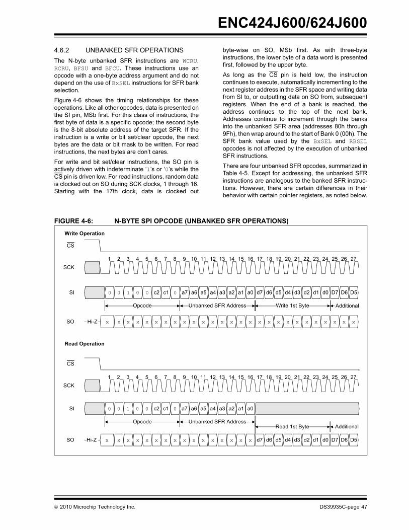
ENC424J600/624J600
4.6.2 UNBANKED SFR OPERATIONS
The N-byte unbanked SFR instructions are WCRU,RCRU, BFSU and BFCU. These instructions use anopcode with a one-byte address argument and do notdepend on the use of BxSEL instructions for SFR bankselection.
Figure 4-6 shows the timing relationships for theseoperations. Like all other opcodes, data is presented onthe SI pin, MSb first. For this class of instructions, thefirst byte of data is a specific opcode; the second byteis the 8-bit absolute address of the target SFR. If theinstruction is a write or bit set/clear opcode, the nextbytes are the data or bit mask to be written. For readinstructions, the next bytes are don’t cares.
For write and bit set/clear instructions, the SO pin isactively driven with indeterminate ‘1’s or ‘0’s while theCS pin is driven low. For read instructions, random datais clocked out on SO during SCK clocks, 1 through 16.Starting with the 17th clock, data is clocked out
byte-wise on SO, MSb first. As with three-byteinstructions, the lower byte of a data word is presentedfirst, followed by the upper byte.
As long as the CS pin is held low, the instructioncontinues to execute, automatically incrementing to thenext register address in the SFR space and writing datafrom SI to, or outputting data on SO from, subsequentregisters. When the end of a bank is reached, theaddress continues to the top of the next bank.Addresses continue to increment through the banksinto the unbanked SFR area (addresses 80h through9Fh), then wrap around to the start of Bank 0 (00h). TheSFR bank value used by the BxSEL and RBSELopcodes is not affected by the execution of unbankedSFR instructions.
There are four unbanked SFR opcodes, summarized inTable 4-5. Except for addressing, the unbanked SFRinstructions are analogous to the banked SFR instruc-tions. However, there are certain differences in theirbehavior with certain pointer registers, as noted below.
FIGURE 4-6: N-BYTE SPI OPCODE (UNBANKED SFR OPERATIONS)
CS
SCK
SI
SO x x x x x x x xHi-Z
a5 a4 a3 a2 a1 a0
x x x
d00 0 c2 d7 d6 d5 d4 d3 d2 d1
x x x x x x x x x x x x x
1 2 3 4 5 6 7 8 9 10 11 12 13 14 15 16 17 18 19 20 21 22 23 24
Opcode Unbanked SFR Address Write 1st Byte
25 26 27
D7 D6 D5
x x x
Additional
0 0 1 c1 0
CS
SCK
SI
SO x x x x x x x xHi-Z
0 0 c2
d7 d6 d5 d4 d3 d2 d1 d0
1 2 3 4 5 6 7 8 9 10 11 12 13 14 15 16 17 18 19 20 21 22 23 24
Opcode Unbanked SFR AddressRead 1st Byte
25 26 27
D7 D6 D5
Additional
0 0 1 c1 0 a5 a4 a3 a2 a1 a0
a6a7
a6a7
x x x x x x x x
Write Operation
Read Operation
2010 Microchip Technology Inc. DS39935C-page 47

ENC424J600/624J600
4.6.2.1 WCRU Opcode
The Write Control Register Unbanked (WCRU) opcodestarts with the opcode, ‘00100010’ (22h), followed bythe unbanked SFR register address during SPI clocks,9 through 16. For example, to write to ECON2L ataddress 6Eh, the instruction would be ‘22h 6Eh’,followed by the data to be written.
When the host controller is finished writing data, it shouldraise the CS line, putting the device in an inactive stateand preparing it for the next SPI instruction. When finish-ing a WCRU transaction, ensure that adequate CS holdtime is provided for the last write to complete beforeraising CS.
Generally, WCRU can be executed on most registeraddresses, in any sequence and for any length. Animportant exception is when WCRU is used on any MACor MII register. These registers must be written aswhole 16-bit registers, low byte first (e.g., MACON1must be written by first writing to MACON1L, thenMACON1H). Writing only to the upper byte of a MAC orMII register results in a successful write to the upperregister, while the lower register is written with indeter-minate data. If a WCRU instruction is aborted by raisingCS while writing to the upper byte of a MAC or MIIregister, neither the upper nor lower byte will beupdated.
In addition, WCRU cannot be used to write to the SRAMbuffer virtual data windows (EGPDATA, ERXDATA andEUDADATA). Writing to the buffer address indicated bythe corresponding address pointers’ attempts has noeffect on the memory location, and the pointers do notauto-increment. To write to the SRAM buffer using thevirtual data windows, always use the SRAM bufferopcodes (WGPDATA, WRXDATA and WUDADATA)instead.
4.6.2.2 RCRU Opcode
The Read Control Register Unbanked (RCRU) opcodestarts with the opcode, ‘00100000’ (20h), followed bythe unbanked SFR register address during SPI clocks,9 through 16. Continuing the previous example, to readECON2L at address 6Eh, the complete two-byteinstruction would be ‘20h 6Eh’.
Read operations can be performed on most registeraddresses, in any sequence and for any length.However, due to volatile register shadowing, it isrecommended that the ERXHEADH:ERXHEADLregister pair be read in sequence (low byte first) toobtain the correct value. See Section 9.2 “ReceivingPackets” for additional information.
Similar to WCRU, RCRU cannot be used to read datafrom the SRAM buffer using the virtual data windows.Reading the buffer address indicated by the corre-sponding address pointers returns indeterminant dataand the pointers do not auto-increment. To read fromthe buffer using the virtual data windows, always usethe SRAM buffer opcodes (RGPDATA, RRXDATA andRUDADATA) instead.
4.6.2.3 BFSU and BFCU Opcodes
The Bit Field Set Unbanked (BFSU) and Bit Filed ClearUnbanked (BFCU) opcodes start with the opcode,‘00100100’ (24h) for BFSU, or ‘00100110’ (26h) forBFCU, followed by the unbanked SFR register addressduring SPI clocks, 9 through 16. In terms of timing andautomatic address increment, they behave almostidentically to the WCRU opcode.
BFSU and BFCU function in the same manner as BFSand BFC, by setting or clearing individual bits in the tar-get register through the use of a bit mask. They are alsoused in the same situations as BFS and BFC; namely,when it is necessary to manipulate a single control bitor interrupt flag in a dynamic situation, while avoidingthe disruption of other bits. See Section 4.6.1.3 “BFSand BFC Opcodes” for a detailed explanation.
TABLE 4-5: N-BYTE UNBANKED SFR INSTRUCTIONS
Note 1: Unlike WCRU, BFSU and BFCU cannot beused to modify MAC or MII registers.Never use these opcodes on MAC andMII registers.
2: BFSU and BFCU opcodes have no effecton any SFR in the unbanked region(addresses 80h through 9Fh).
Instruction MnemonicOpcode Argument
1st Byte 2nd Byte 3rd Byte Nth Byte
Read Control Register(s), Unbanked RCRU 0010 0000 AAAA AAAA xxxx xxxx XXXX XXXX
Write Control Register(s), Unbanked WCRU 0010 0010 AAAA AAAA dddd dddd DDDD DDDD
Bit Field(s) Set, Unbanked BFSU 0010 0100 AAAA AAAA dddd dddd DDDD DDDD
Bit Field(s) Clear, Unbanked BFCU 0010 0110 AAAA AAAA dddd dddd DDDD DDDD
Legend: x/X = read data (LSB/MSB), d/D = write data (LSB/MSB), A = unbanked SFR address. ‘X’ and ‘D’ are optional.
DS39935C-page 48 2010 Microchip Technology Inc.

ENC424J600/624J600
4.6.3 SRAM BUFFER OPERATIONS
The six N-byte SRAM instructions function in a similarmanner to the banked SFR instructions, in that they usea single byte opcode to define the operation and targetregister. In terms of timing, they are virtually identical, asshown in Figure 4-7.
Like all other opcodes, data is presented on the SI pin,MSb first. For all instructions, the first byte of data is theopcode. If the instruction is a write opcode, the nextbytes are the data to be written. For read instructions,the next bytes are don’t cares.
For write instructions, the SO pin is actively driven withindeterminate ‘1’s or ‘0’s while the CS pin is driven low.For read instructions, random data is clocked out on
SO during SCK clocks, 1 through 8. Starting with the9th clock, data is clocked out byte-wise on SO, MSbfirst.
As long as the CS pin is held low, the instructioncontinues to execute, automatically incrementing to thenext SRAM address according to the pointer wrappingrules described in Section 3.5.5 “Indirect SRAM BufferAccess”. The associated read or write pointer SFRs areautomatically updated for each 8 SCK clocks. Toterminate the read or write operation, the CS signal mustbe returned high.
There are 6 instructions divided equally between readand write instructions. They are summarized inTable 4-6.
FIGURE 4-7: N-BYTE SPI OPCODE (SRAM BUFFER OPERATIONS)
CS
SCK
SI
SO x x x x x x x xHi-Z
d5 d4 d3 d2 d1d6d7 d0
x x x
D0c4 c3 c2 D7 D6 D5 D4 D3 D2 D1
x x x x x x x x x x x x x
1 2 3 4 5 6 7 8 9 10 11 12 13 14 15 16 17 18 19 20 21 22 23 24
Opcode Write 1st ByteWrite 2nd Byte
(optional)
25 26 27
D7 D6 D5
x x x
Additional
0 0 1 1 0
CS
SCK
SI
SO x x x x x x x xHi-Z D7 D6 D5
c4 c3 c2
d7 d6 d5 d4 d3 d2 d1 d0 D4 D3 D2 D1 D0
1 2 3 4 5 6 7 8 9 10 11 12 13 14 15 16 17 18 19 20 21 22 23 24
OpcodeRead 1st Byte Read 2nd Byte
(optional)
25 26 27
D7 D6 D5
Additional
0 0 1 0 0
Write Operation
Read Operation
2010 Microchip Technology Inc. DS39935C-page 49

ENC424J600/624J600
TABLE 4-6: N-BYTE SRAM INSTRUCTIONS
Instruction MnemonicOpcode Argument
1st Byte 2nd Byte 3rd Byte Nth Byte
Read Data from EGPDATA RGPDATA 0010 1000 xxxx xxxx XXXX XXXX XXXX XXXX
Write Data from EGPDATA WGPDATA 0010 1010 dddd dddd DDDD DDDD DDDD DDDD
Read Data from ERXDATA RRXDATA 0010 1100 xxxx xxxx XXXX XXXX XXXX XXXX
Write Data from ERXDATA WRXDATA 0010 1110 dddd dddd DDDD DDDD DDDD DDDD
Read Data from EUDADATA RUDADATA 0011 0000 xxxx xxxx XXXX XXXX XXXX XXXX
Write Data from EUDADATA WUDADATA 0011 0010 dddd dddd DDDD DDDD DDDD DDDD
Legend: x/X = read data (LSB/MSB), d/D = write data (LSB/MSB). ‘X’ and ‘D’ are optional.
DS39935C-page 50 2010 Microchip Technology Inc.

ENC424J600/624J600
5.0 PARALLEL SLAVE PORT INTERFACE (PSP)
ENC424J600/624J600 devices are designed tointerface directly with the parallel port available onmany microcontrollers, including the Parallel MasterPort (PMP) available on many Microchip PIC® micro-controllers. The Parallel Slave Port interface is highlyflexible, and can communicate using either Intel® orMotorola® formats for read and write control strobes. Inthe event that a parallel port is not available on the hostmicrocontroller, a software-managed parallel interfacederived from general purpose I/O pins can be used.
When the PSP interface is enabled, the ENCX24J600functions as a slave device on the parallel bus. Thehost controller must be configured to generate thedestination or target address on the slave device, aswell as the necessary port control signals.
5.1 Physical Implementation
The PSP interface is mutually exclusive with the serialinterface. To enable the PSP and disable the SPI, tiethe INT/SPISEL pin to Vss through an external resistor.
The PSP interface can use from 12 to 34 pins, depend-ing on the device pin count and the PSP operatingmode. There are up to eight modes, covering thepermutations of data widths, data/address multiplexingand bus strobe formats. The modes are selected by
tieing each of the PSPCFG<4:0> pins to either VDD orVSS. The available combinations along with relativeperformance metrics are summarized in Table 5-1.Additional information on physical connections areprovided in Section 2.7.2 “PSP”.
In PSP mode, the CS/CS pin becomes the active-highChip Select (CS) pin. A weak internal pull-down is auto-matically connected to the pin when the PSP interfaceis selected, preventing the pin from floating to anindeterminate state when an external Chip Selectsignal is absent.
When CS is in the inactive (logic-low) state, the AD15(64-pin devices only) and AD<14:0> pins are placed ina high-impedance state and are 5V tolerant. Thisallows the ENCX24J600 to share a single parallel buswith other slave devices that function the same waywhile deselected. All other PSP pins, including theA<14:0> pins (64-pin devices only) and the port controlstrobes, are 5V tolerant inputs at all times. Inputs onthese pins are ignored while the chip select pin is atlogic low.
Unlike the SPI port, the use of chip select is optionalwith the PSP. The CS pin can be tied permanently toVDD if the parallel bus is not shared with other slavedevices. This saves one I/O pin from the host controllerwhile leaving the ENCX24J600 in a perpetuallyselected state.
TABLE 5-1: OPERATING MODES SUPPORTED BY THE PSP INTERFACE
PSP Mode
Availability # Pins(1)
Data Width
Address/Data Multiplexing
Control Lines
Theoretical Performance
@ 10 MHz (Mbit/s)
44-pin 64-pin Min Max
1 X 19 26 8 bit No CS, RD, WR 80
2 X 19 26 8 bit No CS, EN, R/W 80
3 X 26 34 16 bit No CS, RD, WRL, WRH 160
4 X 26 34 16 bit No CS, R/W, B0SEL, B1SEL 160
5 X X 12 19 8 bit Yes AL, CS, RD, WR <80
6 X X 12 19 8 bit Yes AL, CS, EN, R/W <80
9 X 19 21 16 bit Yes AL, CS, RD, WRL, WRH <80
10 X 19 21 16 bit Yes AL, CS, R/W, B0SEL, B1SEL
<80
Note 1: Includes only address, data and port control strobes. INT/SPISEL and PSPCFG pins used for mode configuration are not included.
2010 Microchip Technology Inc. DS39935C-page 51

ENC424J600/624J600
5.2 Using the PSP Interface
Unlike the serial interface, the PSP interface does notuse opcodes or a command architecture to control thedevice. Instead, the memory space is accessed directlyusing the addressing schemes described inSection 3.1.2 “PSP Interface Maps”. Control SFRsare read and written to directly, or manipulated throughtheir accompanying Bit Set and Bit Clear registers.
In 16-bit modes, each address (from 0 to 16,384) pointsto a different word. The individual write high and writelow strobes allow the upper or lower byte of each wordto be written individually.
5.2.1 DIRECT AND INDIRECT SRAM BUFFER ACCESS
Direct addressing allows the host controller to accessall SFRs and SRAM buffer addresses in theENCX24J600 memory space directly. This provides thegreatest flexibility and speed for accessing the SRAMbuffer. However, this configuration requires up to15 address pins to be driven by the host controller. Thismay be prohibitive in smaller, pin-constrainedapplications.
In Modes 1 through 6, it is possible to conserve sixaddress pins by tying them to VDD. In this configuration,only the addresses corresponding to the SFR area ofthe memory space can be directly addressed. TheSRAM buffer memory can still be accessed, but onlythrough the EGPDATA, ERXDATA and EUDADATAdata windows in the SFR space, described inSection 3.5.5 “Indirect SRAM Buffer Access”.
Indirect buffer access works well for Multiplexedmodes, such as PSP Modes 5, 6, 9 and 10. In thesemodes, the auto-incrementing feature of the DataWindow Pointers allows access to the buffer at speedssimilar to byte-wise demultiplexed access, since aseparate address phase in not required for each byte.
The 8-Bit PSP modes have separate addresses for thelow and high bytes of each register. Since thesemodes, therefore, have a “longer” memory space (i.e.,more individual addresses), indirect access requires9 lines to address all registers between 7E00h and7FFFh. In contrast, the 16-bit modes require only8 lines to address all of the registers in their SFR range(3F00h to 3FFFh). Even so, using indirect access stillsaves six pins in either data width: AD<14:9> in 8-bitmodes and AD<13:8> in 16-bit modes.
5.2.2 ADDRESS LATCHING
In Multiplexed Address/Data modes (PSP Modes 5through 10), the ENCX24J600 implements an internaladdress latch. This allows a reduction in the total numberof interface pins by multiplexing the data and addressesthat need to be communicated onto a single bus.
In 8-bit modes, the address latch is implemented on allof the AD pins. In 16-bit modes, the address latch isimplemented for only the AD<13:0> pins. Because itspans all required address lines, it is necessary topresent the desired address to the ENCX24J600 foronly a brief period while strobing the Address Latch(AL) pin. On 8-bit interfaces, where AD<14:8> are usedexclusively for addressing, it is not necessary to drivethese upper address lines with a valid addresscontinually through read and write operations.
During operation, strobing the AL pin high and then lowcauses the address presented on the AD pins to besaved to the address latch. The address is retained forall future read and write operations. It is retained untileither a POR event occurs or a subsequent write to theaddress latch occurs by restrobing AL. This allowsmultiple read and write requests to take place to thesame address, without requiring multiple addresslatching operations.
The address latch does not auto-increment afteraccesses. However, by using the indirect buffer accessmethod, it is possible to sequentially read or write anentire array of sequential SRAM locations withoutupdating the address latch.
5.2.3 WRITE SELECT PINS
The 16-Bit PSP modes make use of either two writepins (WRL and WRH), or a R/W select and two ByteLane (B0SEL and B1SEL) controls. When writing to thedevice, these pins allow the host controller to instructwhether to write only the low byte, only the high byte orboth bytes.
If only one write select pin is available on the host con-troller, the high and low selection pins may be tiedtogether to create a single 16-bit write strobe. When thisis done, only word writes are possible. However, the hostcontroller can still write single bytes when accessing theSRAM buffer through the EGPDATA, ERXDATA orEUDADATA Window registers, which always perform8-bit accesses.
5.2.4 UNUSED INTERFACE PINS
Any unused PSP pins are placed in a high-impedancestate, regardless of the state of the CS pin. Formaximum ESD performance, it is recommended thatunused interface pins not be allowed to float. Instead, itis recommended that unused interface pins be tied toeither VSS or VDD.
DS39935C-page 52 2010 Microchip Technology Inc.

ENC424J600/624J600
5.2.5 PERFORMANCE CONSIDERATIONS
When using a 16-bit data bus width, all registers anddirect access to SRAM can be accomplished through16-bit accesses. Therefore, these modes are poten-tially twice as fast as their 8-bit equivalent parallelmode. However, accesses through thehardware-managed SRAM read/write registers,EGPDATA, ERXDATA and EUDADATA, are always8-bit regardless of the interface used. Therefore, inmany applications, it will not be practically feasible totransfer 16 bits of meaningful data for all bus transfercycles.
When reading from the EGPDATA, ERXDATA andEUDADATA registers on an interface with a multi-plexed address bus, it is possible to latch the addressonly once and then perform back-to-back reads orwrites without performing additional address latchcycles. This can provide a significant performanceimprovement when sequentially reading or writing anarray of data to/from the RAM. Due to this benefit, 8-BitMultiplexed modes (Modes 5 and 6) approach thetheoretical performance of the Demultiplexed PSPModes 1 and 2.
5.3 PSP Modes
The eight PSP modes are selected using the PSPCFGpins. The address/data bus and port control connec-tions differ between the modes, sometimessignificantly, as do the timing relationships betweenaddress/data and control signals. Each of the modes isdescribed in detail in the following sections.
5.3.1 MODE 1
PSP Mode 1 is an 8-bit, fully demultiplexed mode thatis available on 64-pin devices only. The parallel inter-face consists of 8 bi-directional data pins (AD<7:0>)and 9 to 15 separate address pins (A<14:0>). To selectPSP Mode 1, tie PSPCFG2, PSPCFG3 and PSPCFG4to VSS. Figure 5-1 shows the connections required.
This mode uses active-high Read and Write strobes(RD and WR) in conjunction with a Chip Select (CS)signal. These three pins allow the host to select thedevice, then signal when a read operation is desired orwhen valid data is being presented to be written. TheAD<7:0> pins stay in a high-impedance state any timeCS or RD is low.
To perform a read operation:
1. Raise the CS line (if connected to the host).
2. Present the address to be read onto the addressbus.
3. Raise the RD strobe and wait the required timefor the access to occur.
When RD is raised high, the data bus begins to driveout indeterminate data for a brief period, then switchesto the correct read data after the appropriate readaccess time has elapsed. When the RD strobe islowered, AD<7:0> return to a high-impedance state.
To perform a write operation:
1. Raise the CS line (if connected to the host).
2. Present the address onto the address bus.
3. Present the data on the data bus.
4. Strobe the WR signal high and then low.
For proper operation, do not raise RD and WRsimultaneously while the ENCX24J600 is selected.
Sample timing diagrams for reading and writing data inthis mode are provided in Figure 5-2 and Figure 5-3,respectively.
2010 Microchip Technology Inc. DS39935C-page 53

ENC424J600/624J600
FIGURE 5-1: DEVICE CONNECTIONS FOR PSP MODE 1
FIGURE 5-2: MODE 1 READ OPERATION TIMING (TWO BYTES)
FIGURE 5-3: MODE 1 WRITE OPERATION TIMING (TWO BYTES)
Host MCU ENC624J600
CS(1)
RD
100 k
WR
A<14:9>(2)
A<8:0>
AD<7:0>
INT/SPISEL
PMCSx
PMRD
PMWR
PMA<14:9>
PMA<8:0>
PMD<7:0>
INTx(3)
6
9
8
PSPCFG2
PSPCFG3
PSPCFG4
Note 1: Use of the CS strobe from the controller is optional. If not used, tie CS to VDD.
2: Connect these pins when direct addressing of the entire SRAM buffer is required. Tie to VDD when only indirectaddressing is desired.
3: Use of the external interrupt signal to the controller is optional.
CS
RD
A<14:0>
AD<7:0> Data<7:0>Hi-Z Hi-Z
Address<14:0> Address<14:0>
Data<7:0> Hi-Z
WR
TPSP1
TPSP2
TPSP4
TPSP3
TPSP6
CS
RD
A<14:0>
AD<7:0> Data<7:0>Hi-Z
Address<14:0> Address<14:0>
Data<7:0> Hi-Z
WR TPSP8
TPSP9
TPSP11
TPSP7 TPSP10
TPSP5
DS39935C-page 54 2010 Microchip Technology Inc.

ENC424J600/624J600
5.3.2 MODE 2
PSP Mode 2 is also an 8-bit, fully demultiplexed modethat is available on 64-pin devices only. The parallelinterface consists of 8 bidirectional data pins (AD<7:0>)and 9 to 15 separate address pins (A<14:0>). To selectPSP Mode 2, tie PSPCFG2 and PSPCFG3 to VSS,while connecting PSPCFG4 to VDD. Figure 5-4demonstrates connections required to use Mode 2.
This mode uses a combined Read/Write (R/W) select,an Enable (EN) strobe pin and a separate Chip Selectpin (CS). These three pins allow the host to select thedevice, indicate whether a read or write operation isdesired and signal when valid data is being presented
A logic high signal on the R/W pin indicates that a readoperation is to be performed when the EN strobe isasserted, while a logic low indicates that a write opera-tion is to be performed. The state of R/W only affectsthe data bus state when the EN signal is active. Wheneither CS, EN or R/W is driven low, the data bus staysin a high-impedance state.
To perform a read operation:
1. Raise the CS line (if connected to the host).
2. Raise the R/W signal.
3. Present the address to be read onto the addressbus.
4. Raise the EN strobe.
5. Wait the required time for the access to occur.
When EN is raised high, the data bus begins to driveout indeterminate data for a brief period, then switchesto the correct read data after the appropriate readaccess time has elapsed. When the EN strobe is low-ered, the data bus pins return to a high-impedancestate.
To perform a write operation:
1. Raise the CS line (if connected to the host).
2. Lower the R/W signal.
3. Present the address onto the address bus.
4. Present the data on the data bus.
5. Strobe the EN signal high and then low.
Sample timing diagrams for reading and writing data inthis mode are provided in Figure 5-5 and Figure 5-6,respectively.
FIGURE 5-4: DEVICE CONNECTIONS FOR PSP MODE 2
Host MCU ENC624J600
CS(1)
R/W
100 k
EN
A<14:9>(2)
A<8:0>
AD<7:0>
INT/SPISEL
PMCSx
PMRD/PMWR
PMENB
PMA<14:9>
PMA<8:0>
PMD<7:0>
INTx(3)
6
9
8
PSPCFG2
PSPCFG3
PSPCFG4
+3.3V
Note 1: Use of the CS strobe from the controller is optional. If not used, tie CS to VDD.
2: Connect these pins when direct addressing of the entire SRAM buffer is required. Tie to VDD when only indirectaddressing is desired.
3: Use of the external interrupt signal to the controller is optional.
2010 Microchip Technology Inc. DS39935C-page 55

ENC424J600/624J600
FIGURE 5-5: MODE 2 READ OPERATION TIMING (TWO BYTES)
FIGURE 5-6: MODE 2 WRITE OPERATION TIMING (TWO BYTES)
CS
A<14:0>
AD<7:0> Data<7:0>Hi-Z Hi-Z
Address<14:0> Address<14:0>
Data<7:0> Hi-Z
EN TPSP1
TPSP2
TPSP4
TPSP3
R/W
TPSP6
CS
A<14:0>
AD<7:0> Data<7:0>Hi-Z
Address<14:0> Address<14:0>
Data<7:0> Hi-Z
EN TPSP8
TPSP9
TPSP11
TPSP7 TPSP10
TPSP5
R/W
DS39935C-page 56 2010 Microchip Technology Inc.

ENC424J600/624J600
5.3.3 MODE 3
PSP Mode 3 is a 16-bit, fully demultiplexed mode thatis available on 64-pin devices only. The parallel inter-face consists of 16 bidirectional data pins (AD<15:0>)and 8 to 14 separate address pins (A<13:0>). To selectPSP Mode 3, tie PSPCFG3 and PSPCFG4 to VSS,while connecting PSPCFG2 to VDD. Figure 5-7 showsthe connections required.
An active-high RD strobe and two Write strobes (WRHand WRL) are utilized in conjunction with a separateChip Select (CS). These four pins allow the host toselect the device, then signal when a read operation isdesired or when valid data is being presented to bewritten on either the low byte, high byte or both. Forproper operation, do not assert CS and RD whilesimultaneously asserting either WRL or WRH.
In PSP Mode 3, AD<15:0> stay in a high-impedancestate any time CS or RD are low.
To perform a read operation:
1. Raise the CS line (if connected to the host).2. Present the address to be read onto the address
bus.
3. Raise the RD strobe and wait the required timefor the access to occur.
When RD is raised high, the data bus begins driving outindeterminate data for a brief period, then switches tothe correct read data after the appropriate read accesstime has elapsed. When the RD strobe is lowered, thedata pins will return to a high-impedance state.
The device always outputs a full 16 bits of data for eachread request. If only 8 bits of data are required, read thedata from the correct pins (AD<15:8> or AD<7:0>) anddiscard the remaining byte.
To perform a write operation:
1. Raise the CS line (if connected to the host).2. Present the address onto the A<13:0> address
bus.
3. If writing to the low byte of the memory location,present the data on AD<7:0>, and strobe theWRL signal high and then low.
4. If writing to the high byte, present the data on theAD<15:8> and strobe the WRH signal.
5. If writing a whole word, strobe both WRL andWRH simultaneously.
Sample timing diagrams for reading and writing data inthis mode are provided in Figure 5-8 and Figure 5-9,respectively.
FIGURE 5-7: DEVICE CONNECTIONS FOR PSP MODE 3
Host MCU ENC624J600
CS(1)
RD
100 k
WRL
A<13:8>(3)
A<7:0>
AD<15:0>
INT/SPISEL
PMCSx
PMRD
PMWRL
PMA<13:8>
PMA<7:0>
PMD<15:0>
INTx(4)
6
8
16
PSPCFG2
PSPCFG3
PSPCFG4
Note 1: Use of the CS strobe from the controller is optional. If not used, tie CS to VDD.
2: WRL and WRH may optionally be tied together to form a 16-bit write strobe. See Section 5.2.3 “Write SelectPins” for details.
3: Connect these pins when direct addressing of the entire SRAM buffer is required. Tie to VDD when only indirectaddressing is desired.
4: Use of the external interrupt signal to the controller is optional.
WRH(2)PMWRH(2)
+3.3V
2010 Microchip Technology Inc. DS39935C-page 57

ENC424J600/624J600
FIGURE 5-8: MODE 3 READ OPERATION TIMING (FOUR BYTES)
FIGURE 5-9: MODE 3 WRITE OPERATION TIMING (THREE BYTES)
CS
RD
A<13:0>
AD<15:0> Data<15:0>Hi-Z Hi-Z
Address<13:0> Address<13:0>
Data<15:0> Hi-Z
WRH
TPSP1
TPSP2
TPSP4
TPSP3
WRL
TPSP6
CS
RD
A<13:0>
AD<15:0> Data<15:0>Hi-Z
Address<13:0> Address<13:0>
Data<7:0> Hi-Z
WRL TPSP8
TPSP9
TPSP11
TPSP7 TPSP10
TPSP5
WRH
DS39935C-page 58 2010 Microchip Technology Inc.

ENC424J600/624J600
5.3.4 MODE 4
PSP Mode 4 is also a 16-bit, fully demultiplexed modethat is available in 64-pin devices only. When usingPSP Mode 4, the parallel interface consists of16 bidirectional data pins (AD<15:0>) and 8 to 14 sep-arate address pins (A<13:0>). To select PSP Mode 4,tie PSPCFG2 and PSPCFG4 to VDD, while connectingPSPCFG3 to VSS. Figure 5-10 shows the connectionsrequired.
This mode uses a combined Read/Write (R/W) select,two Byte Select (B0SEL and B1SEL) lines and a sepa-rate Chip Select (CS) signal. These four pins allow thehost to select the device, indicate whether a read orwrite operation is desired and signal when valid data isbeing presented for writing on either the low byte, highbyte or both.
A logic-high signal on R/W indicates that a read opera-tion is to be performed when either the B0SEL orB1SEL strobe is asserted, while a logic low signalindicates that a write operation is to be performed. Thestate of R/W only affects the data bus state when eitherB0SEL or B1SEL is active. When CS is driven low, R/Wis driven low, or both B0SEL and B1SEL are driven lowand the data bus stays in a high-impedance state.
To perform a read operation:
1. Raise the CS line (if connected to the host).
2. Raise the R/W signal.
3. Present the address to be read onto the address bus.
4. Raise one or both byte select strobes.
When either BxSEL pin is raised high, the data busbegins driving out indeterminate data for a brief period,then switches to the correct read data after the appro-priate read access time has elapsed. When B0SEL andB1SEL are both low, the data bus pins return to ahigh-impedance state.
The device always outputs a full 16 bits of data for eachread request, even if only one byte select is strobed. Ifonly 8 bits of data are required, read the data from thecorrect pins (AD<15:8> or AD<7:0>) and discard theremaining byte.
To perform a write operation:
1. Raise the CS line (if connected to the host).
2. Lower R/W.
3. Present the address onto the address bus.
4. If writing to the low byte of the memory location,present the data on the AD<7:0>; then strobeB0SEL high, then low.
5. If writing to the high byte, present the data onAD<15:8> and strobe B1SEL.
6. If writing a whole word, strobe both B0SEL andB1SEL simultaneously.
Sample timing diagrams for reading and writing data inthis mode are provided in Figure 5-11 and Figure 5-12,respectively.
FIGURE 5-10: DEVICE CONNECTIONS FOR PSP MODE 4
Host MCU ENC624J600
CS(1)
R/W
100 k
B0SEL
A<13:8>(3)
A<7:0>
AD<15:0>
INT/SPISEL
PMCSx
PMRD/PMWR
PMENB0
PMA<13:8>
PMA<7:0>
PMD<15:0>
INTx(4)
6
8
16
PSPCFG2
PSPCFG3
PSPCFG4
B1SEL(2)PMENB1(2)
+3.3V
Note 1: Use of the CS strobe from the controller is optional. If not used, tie CS to VDD.
2: B0SEL and B1SEL may optionally be tied together to form a 16-bit write strobe. See Section 5.2.3 “WriteSelect Pins” for details.
3: Connect these pins when direct addressing of the entire SRAM buffer is required. Tie to VDD when only indirectaddressing is desired.
4: Use of the external interrupt signal to the controller is optional.
2010 Microchip Technology Inc. DS39935C-page 59

ENC424J600/624J600
FIGURE 5-11: MODE 4 READ OPERATION TIMING (FOUR BYTES)
FIGURE 5-12: MODE 4 WRITE OPERATION TIMING (THREE BYTES)
CS
A<13:0>
AD<15:0> Data<15:0>Hi-Z Hi-Z
Address<13:0> Address<13:0>
Data<15:0> Hi-Z
B1SEL
TPSP2 TPSP3
B0SEL TPSP1 TPSP4
R/W
TPSP6
CS
A<13:0>
AD<15:0> Data<15:0>Hi-Z
Address<13:0> Address<13:0>
Data<7:0> Hi-Z
B1SEL
TPSP9
TPSP7 TPSP10
TPSP5
B0SEL TPSP8 TPSP11
R/W
DS39935C-page 60 2010 Microchip Technology Inc.

ENC424J600/624J600
5.3.5 MODE 5
PSP Mode 5 is an 8-bit, partially multiplexed mode thatis available on all devices. The parallel interface con-sists of 8 multiplexed address and data pins (AD<7:0>),plus one required high address bit (AD8) and 6 optionaladdress-only pins (AD<14:9>).
Selecting PSP Mode 5 differs between 44-pin and64-pin devices, as shown in Figure 5-13. For the 44-pinENC424J600, tie PSPCFG0 to VSS. For the 64-pinENC624J600, tie PSPCFG1 and PSPCFG2 to VSS,and PSPCFG3 to VDD.
This mode uses active-high Read and Write (RD andWR) strobes, as well as separate Chip Select andAddress Latch (CS and AL) lines. These four pins allowthe host to select the device, latch an address, thenindicate when a read or write operation is desired. Forproper operation, treat the RD, WR and AL strobes asmutually exclusive whenever the ENCX24J600 isselected. Only raise one of these to logic high at anygiven time.
AD<14:8> are used as address inputs only, and aretherefore, always left in a high-impedance state. WhenCS or RD is driven low, the multiplexed AD<7:0> pinsstay in a high-impedance state.
To perform a read operation:
1. Raise CS (if connected to the host).
2. Present the address to read from on AD<14:0>.
3. Strobe the AL pin high and low.
4. Set the host controller’s AD<7:0> bus pins asinputs.
5. Raise RD.
The AD<7:0> bus begins driving out indeterminate datafor a brief period, then switches to the correct read dataafter the appropriate read access time has elapsed.When RD is lowered, the AD<7:0> pins return to ahigh-impedance state.
To perform a write operation:
1. Raise CS (if connected to the host).
2. Present the address to write to on AD<14:0>.
3. Strobe the AL pin.
4. Change the data on AD<7:0> from the loweraddress byte to the data to be written.
5. Strobe WR high and then low.
If a subsequent read or write of the same memoryaddress is desired, it is possible to restrobe RD or WRwithout going through another address latch cycle.
Sample timing diagrams for reading and writing data inthis mode are provided in Figure 5-14 and Figure 5-15,respectively.
2010 Microchip Technology Inc. DS39935C-page 61

ENC424J600/624J600
FIGURE 5-13: DEVICE CONNECTIONS FOR PSP MODE 5
Host MCU ENC424J600
CS(1)
RD
100 k
WR
AD<14:9>(2)
AD<7:0>
INT/SPISEL
PMCSx
PMRD
PMWR
PMA<14:9>
PMD<7:0>
INTx(3)
6
8
PSPCFG0
Note 1: Use of the CS strobe from the controller is optional. If not used, tie CS to VDD.
2: Connect these pins when direct addressing of the entire SRAM buffer is required. Tie to VDD when only indirectaddressing is desired.
3: Use of the external interrupt signal to the controller is optional.
Host MCU ENC624J600
100 k
INT/SPISELINTx(3)
PSPCFG1
PSPCFG2
PSPCFG3
ALPMALL
CS(1)
RD
WR
PMCSx
PMRD
PMWR
6
ALPMALL
+3.3V
44-pin Devices:
64-pin Devices:
PMA8 AD8
AD<14:9>(2)
AD<7:0>
PMA<14:9>
PMD<7:0>8
PMA8 AD8
DS39935C-page 62 2010 Microchip Technology Inc.

ENC424J600/624J600
FIGURE 5-14: MODE 5 READ OPERATION TIMING (TWO BYTES – SAME ADDRESS)
FIGURE 5-15: MODE 5 WRITE OPERATION TIMING (TWO BYTES – SAME ADDRESS)
CS
RD
AD<14:9>(1)
WR
AL
Note 1: AD8 must be driven by the host controller. AD<14:9> may be tied to logic high when only indirect access is desired.
Address<14:9>
AD8(1) Address<8>
AD<7:0> Data<7:0>Hi-Z Hi-Z Hi-ZAddress<7:0>
TPSP13
TPSP12
TPSP12
TPSP15
TPSP2 TPSP3
TPSP4
Data<7:0>
TPSP14
CS
RD
AD<14:9>(1)
WR
AL
Note 1: AD8 must be driven by the host controller. AD<14:9> may be tied to logic high when only indirect access is desired.
Address<14:9>
AD8(1) Address<8>
AD<7:0> Data<7:0>Hi-Z Hi-ZAddress<7:0>
TPSP13
TPSP12
TPSP12
TPSP8
TPSP10
TPSP11
Data<7:0>
TPSP7
TPSP14
2010 Microchip Technology Inc. DS39935C-page 63
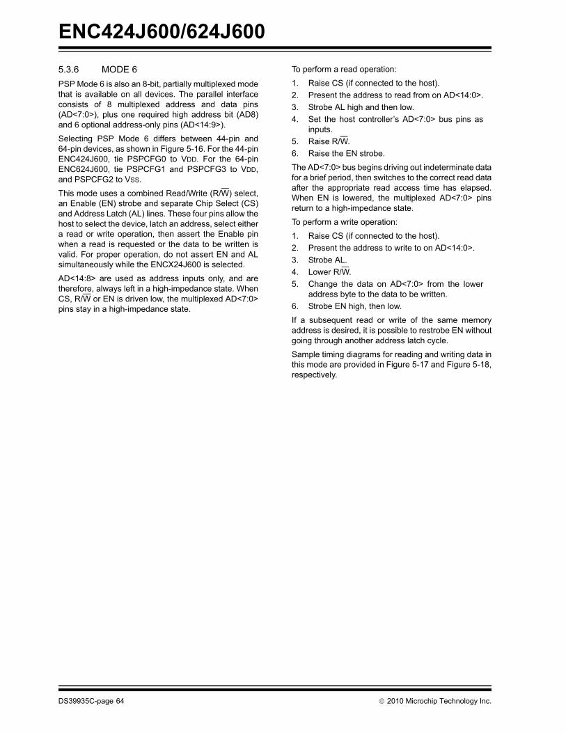
ENC424J600/624J600
5.3.6 MODE 6
PSP Mode 6 is also an 8-bit, partially multiplexed modethat is available on all devices. The parallel interfaceconsists of 8 multiplexed address and data pins(AD<7:0>), plus one required high address bit (AD8)and 6 optional address-only pins (AD<14:9>).
Selecting PSP Mode 6 differs between 44-pin and64-pin devices, as shown in Figure 5-16. For the 44-pinENC424J600, tie PSPCFG0 to VDD. For the 64-pinENC624J600, tie PSPCFG1 and PSPCFG3 to VDD,and PSPCFG2 to VSS.
This mode uses a combined Read/Write (R/W) select,an Enable (EN) strobe and separate Chip Select (CS)and Address Latch (AL) lines. These four pins allow thehost to select the device, latch an address, select eithera read or write operation, then assert the Enable pinwhen a read is requested or the data to be written isvalid. For proper operation, do not assert EN and ALsimultaneously while the ENCX24J600 is selected.
AD<14:8> are used as address inputs only, and aretherefore, always left in a high-impedance state. WhenCS, R/W or EN is driven low, the multiplexed AD<7:0>pins stay in a high-impedance state.
To perform a read operation:
1. Raise CS (if connected to the host).
2. Present the address to read from on AD<14:0>.
3. Strobe AL high and then low.
4. Set the host controller’s AD<7:0> bus pins asinputs.
5. Raise R/W.
6. Raise the EN strobe.
The AD<7:0> bus begins driving out indeterminate datafor a brief period, then switches to the correct read dataafter the appropriate read access time has elapsed.When EN is lowered, the multiplexed AD<7:0> pinsreturn to a high-impedance state.
To perform a write operation:
1. Raise CS (if connected to the host).
2. Present the address to write to on AD<14:0>.
3. Strobe AL.
4. Lower R/W.
5. Change the data on AD<7:0> from the loweraddress byte to the data to be written.
6. Strobe EN high, then low.
If a subsequent read or write of the same memoryaddress is desired, it is possible to restrobe EN withoutgoing through another address latch cycle.
Sample timing diagrams for reading and writing data inthis mode are provided in Figure 5-17 and Figure 5-18,respectively.
DS39935C-page 64 2010 Microchip Technology Inc.

ENC424J600/624J600
FIGURE 5-16: DEVICE CONNECTIONS FOR PSP MODE 6
Host MCU ENC424J600
CS(1)
R/W
100 k
EN
AD<14:9>(2)
AD<7:0>
INT/SPISEL
PMCSx
PMRD/PMWR
PMENB
PMA<14:9>
PMD<7:0>
INTx(3)
6
8
PSPCFG0
Note 1: Use of the CS strobe from the controller is optional. If not used, tie CS to VDD.
2: Connect these pins when direct addressing of the entire SRAM buffer is required. Tie to VDD when only indirectaddressing is desired.
3: Use of the external interrupt signal to the controller is optional.
Host MCU ENC624J600
100 k
INT/SPISELINTx(3)
PSPCFG1
PSPCFG2
PSPCFG3
ALPMALL
6
+3.3V
44-pin Devices:
64-pin Devices:
PMA8 AD8
AD<14:9>(2)
AD<7:0>
PMA<14:9>
PMD<7:0>8
PMA8 AD8
+3.3V
CS(1)
R/W
EN
PMCSx
PMRD/PMWR
PMENBALPMALL
2010 Microchip Technology Inc. DS39935C-page 65

ENC424J600/624J600
FIGURE 5-17: MODE 6 READ OPERATION TIMING (TWO BYTES – SAME ADDRESS)
FIGURE 5-18: MODE 6 WRITE OPERATION TIMING (TWO BYTES – SAME ADDRESS)
CS
EN
AD<14:9>(1)
AL
Note 1: AD8 must be driven by the host controller. AD<14:9> may be tied to logic high when only indirect access is desired .
Address<14:9>
AD8(1) Address<8>
AD<7:0> Data<7:0>Hi-Z Hi-Z Hi-ZAddress<7:0>
TPSP13
TPSP12
TPSP12
TPSP15
TPSP2 TPSP3
TPSP4
Data<7:0>
TPSP1
TPSP14
R/W
CS
AD<14:9>(1)
EN
AL
Note 1: AD8 must be driven by the host controller. AD<14:9> may be tied to logic high when only indirect access is desired .
Address<14:9>
AD8(1) Address<8>
AD<7:0> Data<7:0>Hi-Z Hi-ZAddress<7:0>
TPSP13
TPSP12
TPSP12
TPSP8
TPSP10
TPSP11
Data<7:0>
TPSP7
TPSP5
TPSP14
R/W
DS39935C-page 66 2010 Microchip Technology Inc.

ENC424J600/624J600
5.3.7 MODE 9
PSP Mode 9 is a 16-bit, fully-multiplexed mode that isavailable on 64-pin devices only. The parallel interfaceconsists of 16 bidirectional data pins (AD<15:0>); thelower 14 (AD<13:0>) also function as address pins. Toselect PSP Mode 9, tie PSPCFG2 and PSPCFG3 toVDD, while connecting PSPCFG1 to VSS. Figure 5-19shows the connections required.
This mode uses an active-high Read (RD) strobe andtwo Write (WRH and WRL) strobes in conjunction withseparate Chip Select (CS) and Address Latch (AL)inputs. These five pins allow the host to select thedevice, latch an address and then signal when a readoperation is desired or when valid data is beingpresented to be written to either the low byte, high byteor both. For proper operation while the ENCX24J600 isselected, do not assert RD or AL while simultaneouslyasserting either WRL or WRH.
AD<15:0> stay in a high-impedance state any time CSor RD is low.
To perform a read operation:
1. Raise CS (if connected to the host).
2. Present the address to read from on AD<13:0>.
3. Strobe AL high, then low.
4. Set the host controller’s AD<15:0> bus pins asinputs.
5. Raise RD.
The AD<15:0> bus begins driving out indeterminatedata for a brief period, then switches to the correct readdata after the appropriate read access time haselapsed. When RD is lowered, the AD<15:0> pinsreturn to a high-impedance state.
The device always outputs a full 16 bits of data for eachread request. If only 8 bits of data are required, read thedata from the correct pins (AD<15:8> or AD<7:0>) anddiscard the remaining byte.
To perform a write operation:
1. Raise CS (if connected to the host).
2. Present the address to write to on AD<13:0>.
3. Strobe AL.
4. If writing to the low byte of the memory location,present the data on AD<7:0>, then strobe WRLhigh, then low.
5. If writing to the high byte, present the data onAD<15:8>, then strobe WRH.
6. If writing a whole word, strobe both WRL andWRH simultaneously.
If a subsequent read or write of the same memoryaddress is desired, it is possible to restrobe RD, WRLor WRH without going through another address latchcycle.
Sample timing diagrams for reading and writing data inthis mode are provided in Figure 5-20 and Figure 5-21,respectively.
FIGURE 5-19: DEVICE CONNECTIONS FOR PSP MODE 9
Host MCU ENC624J600
100 k
AD<15:0>
INT/SPISEL
PMD<15:0>
INTx(3)
16
PSPCFG1
PSPCFG2
PSPCFG3
CS(1)
RD
WRL
PMCSx
PMRD
PMWRLWRH(2)PMWRH
(2)
ALPMALL
Note 1: Use of the CS strobe from the controller is optional. If not used, tie CS to VDD.
2: WRL and WRH may optionally be tied together to form a 16-bit write strobe. See Section 5.2.3 “Write SelectPins” for details.
3: Use of the external interrupt signal to the controller is optional.
+3.3V
2010 Microchip Technology Inc. DS39935C-page 67

ENC424J600/624J600
FIGURE 5-20: MODE 9 READ OPERATION TIMING (FOUR BYTES – SAME ADDRESS)
FIGURE 5-21: MODE 9 WRITE OPERATION TIMING (THREE BYTES – SAME ADDRESS)
CS
RD
WRL
AL
AD<15:0> Data<15:0>Hi-Z Hi-Z Hi-ZAddress<13:0>
TPSP13
TPSP12
TPSP12
TPSP15
TPSP2 TPSP3
TPSP4
Data<15:0>
WRH
TPSP14
CS
RD
WRL
AL
AD<15:0> Data<15:0>Hi-Z Hi-ZAddress<13:0>
TPSP13
TPSP12
TPSP12
TPSP8
TPSP10
TPSP11
Data<7:0>
TPSP7
WRH
TPSP14
DS39935C-page 68 2010 Microchip Technology Inc.

ENC424J600/624J600
5.3.8 MODE 10
PSP Mode 10 is also a 16-bit, fully-multiplexed modethat is available on 64-pin devices only. The parallelinterface consists of 16 bidirectional data pins(AD<15:0>); the lower 14 (AD<13:0>) also function asaddress pins. To select PSP Mode 10, tie PSPCFG1,PSPCFG2 and PSPCFG3 to VDD. Figure 5-22 showsthe connections required.
This mode uses an active-high Read/Write (R/W)select and two Byte Select (B0SEL and B1SEL)strobes in conjunction with separate Chip Select (CS)and Address Latch (AL) inputs. These five pins allowthe host to select the device, latch an address, selecteither a read or write operation, then assert the properByte Select strobe(s) to perform the operation.
A logic high signal on the R/W pin indicates that a readoperation is to be performed when either the B0SEL orB1SEL strobe is asserted, while a logic low signalindicates that a write operation is to be performed. Forproper operation while the ENCX24J600 is selected,the host controller should not assert AL whilesimultaneously asserting either B0SEL or B1SEL.
The state of R/W only affects the AD<15:0> bus statewhen either B0SEL or B1SEL is active. When CS isdriven low, R/W is driven low, or both B0SEL andB1SEL are driven low, AD<15:0> stays in ahigh-impedance state.
To perform a read operation:
1. Raise CS (if connected to the host).2. Present the address to be read onto AD<13:0>.3. Strobe AL high, then low.4. Raise R/W.5. Set the host controller’s AD<15:0> bus pins as
inputs.6. Raise either B0SEL or B1SEL, or both.
When either BxSEL pin is raised high, the AD<15:0>bus begins driving out indeterminate data for a briefperiod, then switches to the correct read data after theappropriate read access time has elapsed. WhenB0SEL and B1SEL are both low, AD<15:0> return to ahigh-impedance state.
The device always outputs a full 16 bits of data for eachread request, even if only one byte select is strobed. Ifonly 8 bits of data are required, read the data from thecorrect pins (AD<15:8> or AD<7:0>) and discard theremaining byte.
To perform a write operation:
1. Raise CS (if connected to the host).2. Present the address to write to on AD<13:0>.3. Strobe AL.4. Lower R/W.
5. If writing to the low byte of the memory location,present the data on AD<7:0>, then strobeB0SEL.
6. If writing to the high byte, present the data onAD<15:8>, then strobe the B1SEL signal.
7. If writing a whole word, strobe both B0SEL andB1SEL simultaneously.
If a subsequent read or write of the same memoryaddress is desired, it is possible to restrobe B0SEL orB1SEL without going through another address latchcycle.
Sample timing diagrams for reading and writing data inthis mode are provided in Figure 5-23 and Figure 5-24,respectively.
FIGURE 5-22: DEVICE CONNECTIONS FOR PSP MODE 1
Host MCU ENC624J600
AD<15:0>PMD<15:0>16
100 k
INT/SPISELINTx(3)
PSPCFG1
PSPCFG2
PSPCFG3
+3.3V
CS(1)
R/W
B0SEL
PMCSx
PMRD/PMWR
PMENB0B1SEL(2)PMENB1
(2)
ALPMALL
Note 1: Use of the CS strobe from the controller is optional. If not used, tie CS to VDD.
2: B0SEL and B1SEL may optionally be tied together to form a 16-bit write strobe. See Section 5.2.3 “Write Select Pins” fordetails.
3: Use of the external interrupt signal to the controller is optional.
2010 Microchip Technology Inc. DS39935C-page 69

ENC424J600/624J600
FIGURE 5-23: MODE 10 READ OPERATION TIMING (FOUR BYTES – SAME ADDRESS)
FIGURE 5-24: MODE 10 WRITE OPERATION TIMING (THREE BYTES – SAME ADDRESS)
CS
B0SEL
AL
AD<15:0> Data<15:0>Hi-Z Hi-Z Hi-ZAddress<13:0>
TPSP13
TPSP12
TPSP12
TPSP15
TPSP2 TPSP3
TPSP4
Data<15:0>
B1SEL
TPSP1
TPSP14
R/W
CS
B0SEL
AL
AD<15:0> Data<15:0>Hi-Z Hi-ZAddress<13:0>
TPSP13
TPSP12
TPSP8
TPSP10
TPSP11
Data<7:0>
B1SEL
TPSP5
TPSP14
R/W
TPSP12 TPSP7
DS39935C-page 70 2010 Microchip Technology Inc.
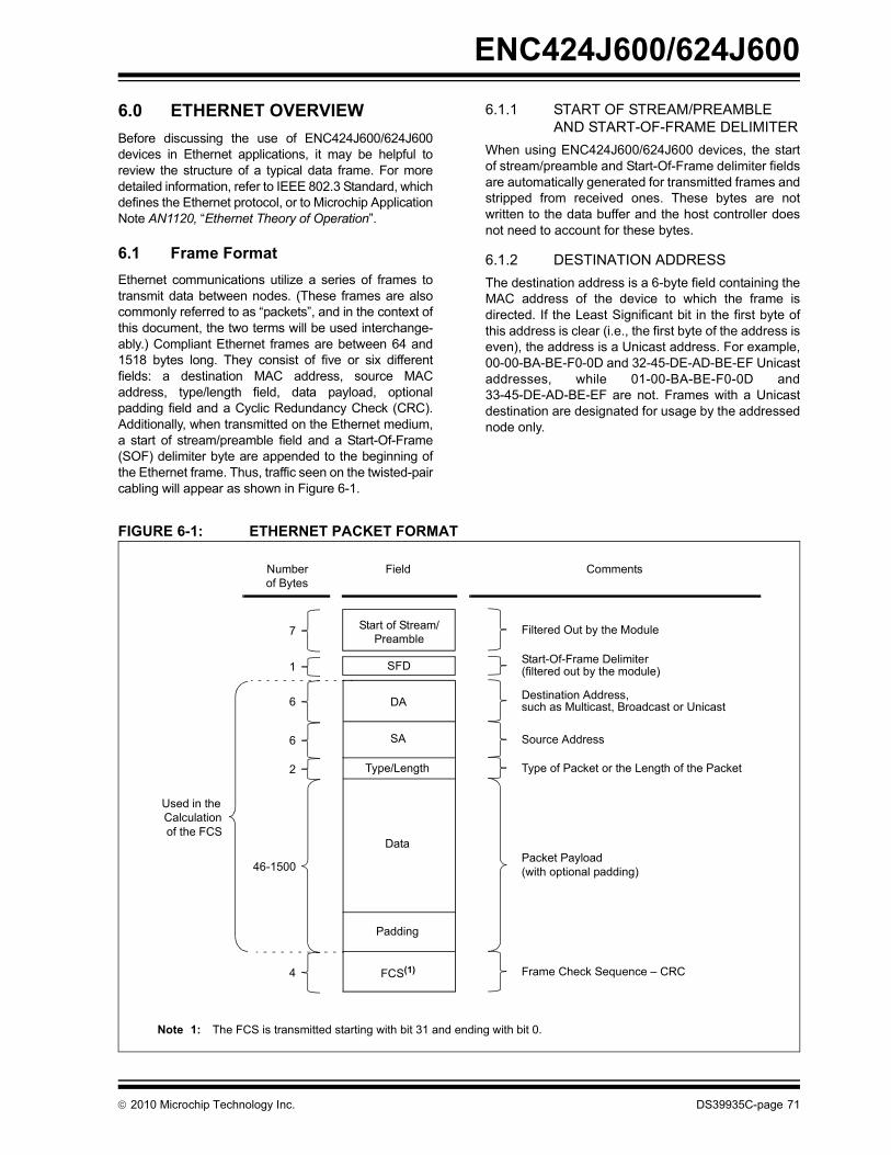
ENC424J600/624J600
6.0 ETHERNET OVERVIEW
Before discussing the use of ENC424J600/624J600devices in Ethernet applications, it may be helpful toreview the structure of a typical data frame. For moredetailed information, refer to IEEE 802.3 Standard, whichdefines the Ethernet protocol, or to Microchip ApplicationNote AN1120, “Ethernet Theory of Operation”.
6.1 Frame Format
Ethernet communications utilize a series of frames totransmit data between nodes. (These frames are alsocommonly referred to as “packets”, and in the context ofthis document, the two terms will be used interchange-ably.) Compliant Ethernet frames are between 64 and1518 bytes long. They consist of five or six differentfields: a destination MAC address, source MACaddress, type/length field, data payload, optionalpadding field and a Cyclic Redundancy Check (CRC).Additionally, when transmitted on the Ethernet medium,a start of stream/preamble field and a Start-Of-Frame(SOF) delimiter byte are appended to the beginning ofthe Ethernet frame. Thus, traffic seen on the twisted-paircabling will appear as shown in Figure 6-1.
6.1.1 START OF STREAM/PREAMBLE AND START-OF-FRAME DELIMITER
When using ENC424J600/624J600 devices, the startof stream/preamble and Start-Of-Frame delimiter fieldsare automatically generated for transmitted frames andstripped from received ones. These bytes are notwritten to the data buffer and the host controller doesnot need to account for these bytes.
6.1.2 DESTINATION ADDRESS
The destination address is a 6-byte field containing theMAC address of the device to which the frame isdirected. If the Least Significant bit in the first byte ofthis address is clear (i.e., the first byte of the address iseven), the address is a Unicast address. For example,00-00-BA-BE-F0-0D and 32-45-DE-AD-BE-EF Unicastaddresses, while 01-00-BA-BE-F0-0D and33-45-DE-AD-BE-EF are not. Frames with a Unicastdestination are designated for usage by the addressednode only.
FIGURE 6-1: ETHERNET PACKET FORMAT
SA
Padding
FCS(1)
Number Field Comments
6
46-1500
4
DADestination Address,such as Multicast, Broadcast or Unicast
Source Address
Packet Payload
Frame Check Sequence – CRC
Type/Length
Data
of Bytes
6
2 Type of Packet or the Length of the Packet
(with optional padding)
7 Filtered Out by the Module
SFD1Start-Of-Frame Delimiter(filtered out by the module)
Used in the Calculation of the FCS
Note 1: The FCS is transmitted starting with bit 31 and ending with bit 0.
PreambleStart of Stream/
2010 Microchip Technology Inc. DS39935C-page 71
ENC424J600/624J600
If the Least Significant bit in the first byte of this addressis set (i.e., the byte is odd), the address is a Multicastdestination. From the previous example,01-00-BA-BE-F0-0D and 33-45-DE-AD-BE-EF areMulticast addresses. Multicast frames are designatedfor use by a selected group of Ethernet nodes. TheMulticast address, FF-FF-FF-FF-FF-FF, is reserved; itis known as the Broadcast address and is directed to allnodes on the network.
ENC424J600/624J600 devices incorporate severalpacket filters which can be configured to accept or dis-card Unicast, Multicast and/or Broadcast frames. Fordetails about these and other receive filters, refer toSection 10.0 “Receive Filters”. When transmittingframes, the host controller is responsible for writing thedesired destination address into the transmit buffer.
6.1.3 SOURCE ADDRESS
The source address is a 6-byte field containing theMAC address of the node which transmitted the Ether-net frame. Every Ethernet device must have a globallyunique MAC address. Each ENC424J600/624J600device has a unique address which is loaded into theMAADR registers on power-up. This value can be usedas is, or the registers may be reconfigured with adifferent address.
6.1.4 TYPE/LENGTH
The type/length field is a 2-byte field indicating the pro-tocol to which the frame belongs. Applications usingstandards such as Internet Protocol (IP) or AddressResolution Protocol (ARP) should use the type codespecified in the appropriate standards document.Alternately, this field can be used as a length field whenimplementing proprietary networks. Typically, anyvalue of 1500 (05DCh) or smaller is considered to be alength field and specifies the amount of non-paddingdata which follows in the data field.
6.1.5 DATA
The data field typically consists of between 0 and1500 bytes of payload data for each frame.ENC424J600/624J600 devices are capable of trans-mitting and receiving frames larger than this when theHuge Frame Enable bit, HFRMEN (MACON2<2>), isset. However, these larger data frames violate Ethernetspecifications and will likely be dropped by mostEthernet nodes.
6.1.6 PADDING
The padding field is a variable length field appended tomeet IEEE 802.3 specification requirements whentransmitting small data payloads. As mentioned, theminimum Ethernet frame size is 64 bytes. Removingthe 18 bytes of address and type information, and theterminating 4-byte CRC, leaves a minimum of 46 bytes.Smaller frames must be padded to fill this space.
When transmitting frames, ENC424J600/624J600devices can automatically generate zero padding if thePADCFG<2:0> bits (MACON2<7:5>) are configured todo so. Otherwise, the application must append theappropriate padding. The device will not prevent thetransmission of these “runt” frames if the hostcommands such an action, but the frame is likely to bedropped by other nodes.
When receiving frames, ENC424J600/624J600 devicesaccept and write all padding to the receive buffer.Frames shorter than the required 64 bytes can optionallybe filtered by the Runt Error Reject filter, described inSection 10.4 “Runt Error Rejection Filter”.
6.1.7 CRC
The CRC is a 4-byte field containing a standard 32-bitCRC calculated over the destination, source, type, dataand padding fields. It allows for the detection oftransmission errors.
When transmitting frames, ENC424J600/624J600devices can automatically generate and append a validCRC if the PADCFG<2:0> bits are configured to do so.Otherwise, the host controller must generate andappend this value. It is strongly recommended that thePADCFG bits be configured so that the hardwareautomatically manages this field.
When receiving frames, ENC424J600/624J600devices accept and write the CRC field to the receivebuffer. Frames with invalid CRC values can bediscarded by the CRC Error Rejection filter, describedin Section 10.3 “CRC Error Rejection Filter”.
DS39935C-page 72 2010 Microchip Technology Inc.

ENC424J600/624J600
7.0 RESET
ENC424J600/624J600 differentiates between fivetypes of Resets:
• Power-on Reset (POR)
• System Reset
• Transmit Only Reset
• Receive Only Reset
• PHY Subsystem Reset
A simplified block diagram of the on-chip Reset circuitis shown in Figure 7-1.
7.1 Power-on Reset
Power-on Reset occurs when VDD rises above VPOR.This allows the device to start in the initialized statewhen VDD is adequate for the device’s digital logic tooperate correctly. The POR circuitry is always enabled.
To ensure proper POR operation, the application circuitmust meet the specified minimum rise rate of VDD
(SVDD, DC parameter D003).
After a Power-on Reset, the contents of the SRAM bufferand cryptographic memories are unknown. However, allregisters will be loaded with their specified Reset values.The PHY and other logic should still not be accessedimmediately after the POR. See Section 8.1 “Reset”for the recommended Reset procedure.
7.2 System Reset
A System Reset reverts all registers back to theirdefault Reset values, with the exception ofCOCON<3:0> (ECON2<11:8>), which controls thefrequency output on CLKOUT. All transmit, receive,MAC, PHY, DMA and cryptographic logic are reset.Additionally, if the SPI interface is used, the currentinternal bank selection is reset to Bank 0. The packetbuffer, cryptographic memories and the PSP addresslatch used in Multiplexed Parallel modes are unaffectedby a System Reset.
To initiate a System Reset, set the ETHRST bit(ECON2<4>). The bit is automatically cleared byhardware. After setting ETHRST, a delay of 25 s isrequired before the ENCX24J600 can be accessedagain through the SPI or PSP interfaces. Additionally,all PHY registers and status bits derived from the PHYshould not be accessed or used for an additional periodof 256 s.
A System Reset does not cause the SPISEL andPSPCFGx pin states to be relatched. Therefore, the cur-rently selected controller interface remains availableafter issuing a System Reset and waiting the required25 s.
FIGURE 7-1: ON-CHIP RESET CIRCUIT
POR Reset SFRs and
Reset TX
Reset RX
Transmit Reset
Receive Reset
System Reset(ETHRST)
Reset I/O Interface and CLKOUT
Reset PHYPHY Reset
(TXRST)
(RXRST)
(PRST)
SPI Bank Select
2010 Microchip Technology Inc. DS39935C-page 73

ENC424J600/624J600
7.3 Transmit Only Reset
A Transmit Only Reset is performed by setting theTXRST bit (ECON2<6>). The transmit logic is held inReset until the bit is cleared. Any pending transmissionis aborted and TXRTS (ECON1<1>) is cleared. Toresume normal operation, clear the TXRST bit.
Both the POR and System Resets automatically performa Transmit Reset, so this step does not need to be per-formed after a System or Power-on Reset. Only thetransmit logic is affected by this operation. Other registerand control blocks are not affected by this event.
7.4 Receive Only Reset
A Receive Only Reset is performed by setting theRXRST bit (ECON2<5>). The receive logic is held inReset until the bit is cleared. Any packet being receivedis aborted and RXEN (ECON1<0>) is cleared. Toresume normal operation, clear the RXRST bit.
Both the POR and System Resets automatically performa Receive Reset, so this step does not need to be per-formed after a System or Power-on Reset. Only thereceive logic is affected by this operation. Other registerand control blocks are not affected by this event.
Following a Receive Only Reset, it is necessary tomanually reconfigure the RX SFRs for normal receiveoperation again. For example, applications must clearthe PKTCNT field in ESTAT by setting the PKTDEC bit(ECON1<8>) enough times for the count to reach zero.Similarly, applications must reset the ERXST andERXTAIL Pointers before enabling reception again withthe RXEN bit.
7.5 PHY Subsystem Reset
The PHY module may be reset by setting the PRST bit(PHCON1<15>). The PHY register contents all revertto their default values.
Unlike the Transmit and Receive Only Resets, the PHYcannot be removed from Reset immediately after settingPRST. The PHY requires a delay, after which thehardware automatically clears the PRST bit. It is recom-mended that, after issuing a Reset, the host controllerpolls PRST and waits for it to be cleared by hardwarebefore using the PHY.
The POR and System Resets automatically perform aPHY Reset, so this step does not need to be performedafter a System or Power-on Reset. Only the PHY isaffected by this operation. Other register and controlblocks are not affected by this event.
DS39935C-page 74 2010 Microchip Technology Inc.

ENC424J600/624J600
8.0 INITIALIZATION
Before using an ENCX24J600 device to transmit andreceive packets, certain device settings must be initial-ized. Depending on the application, some configurationoptions may be left set to their default values. Thosethat need to be changed are typically set once afterpower-up and not changed thereafter.
8.1 Reset
Because it is possible for the host controller to resetindependently from the ENCX24J600 (for example,when using an external debugger to reprogram thehost), it is recommended that software issue a SystemReset of the ENCX24J600 as the first step of itsordinary initialization routine.
Also, since it is possible for the host controller to exit itsPOR, begin code execution before the ENCX24J600exits POR and latches the Interface mode, special careshould be taken in the software to ensure that it doesnot attempt to blindly initialize the ENCX24J600registers before the device is actually out of Reset. Totake care of these potential pitfalls, it is recommendedthat firmware take a write-verify-reset-reverifyapproach to ensure proper start-up. For example:
1. Write 1234h to EUDAST.
2. Read EUDAST to see if it now equals 1234h. Ifit does not, the SPI/PSP interface may not beready yet, so return to step 1 and try again.
3. Poll CLKRDY (ESTAT<12>) and wait for it tobecome set.
4. Issue a System Reset command by settingETHRST (ECON2<4>).
5. In software, wait at least 25 s for the Reset totake place and the SPI/PSP interface to beginoperating again.
6. Read EUDAST to confirm that the System Resettook place. EUDAST should have reverted backto its Reset default of 0000h.
7. Wait at least 256 s for the PHY registers andPHY status bits to become available.
The ENCX24J600 is now ready to accept furthercommands.
8.2 CLKOUT Frequency
If the ENCX24J600 is providing a system clock for thehost controller, or other hardware features of theapplication, it is recommended that the application con-figure the output frequency on the CLKOUT pin first.The frequency is set by using the COCON<3:0> bits(ECON2<11:8>). By default, the output frequency onCLKOUT after a POR is 4 MHz. The last programmedfrequency is maintained after all other Reset events.
For more information on using the output of theCLKOUT pin, see Section 2.2 “CLKOUT Pin”.
8.3 Receive Buffer
Before packet reception is enabled, the receive buffermust be configured by programming the ERXSTPointer. All memory between this pointer and the end ofthe physical memory (5FFFh), including thoseaddresses, are reserved as the receive buffer forincoming packets. The value of ERXST must beword-aligned, since all incoming frames must be storedbeginning at even addresses.
If an application expects a large amount of incomingtraffic or frequent packet delivery, it is recommendedthat it allocate a larger receive buffer. Applicationsneeding more space for saving old packets or othertemporary storage, or wishing to hold several packetsready for transmission, can allocate less memory forthe receive buffer.
Reception of incoming packets begins at the addressdesignated by ERXST.
8.4 Transmit Buffer
No specific transmit buffer is defined. The host applica-tions may write frames to be transmitted to any unusedspace in the SRAM buffer; no initialization is necessary.
8.5 Receive Filters
Before enabling packet reception, configure the receivefilters to eliminate unwanted incoming packets. SeeSection 10.0 “Receive Filters” for details.
8.6 MAC Initialization
Once the receive buffer and filters are properlyconfigured, several MAC registers must be configured.The order of programming is unimportant.
• If flow control operation is desired, configure the flow control module as described in Section 11.0 “Flow Control”.
• Verify that the TXCRCEN (MACON2<4>) and PADCFG<2:0> (MACON2<7:5>) bits are set correctly. Most applications will not need to modify these settings from their power-on defaults.
• Program the MAMXFL register with the maximum frame length to be accepted (received or transmit-ted). Most network nodes are configured to handle packets that are 1518 bytes or less (1522 bytes or less if VLAN tagging is used). Alternately, set HFRMEN (MACON2<2>) to accept any size frame.
• Set the RXEN bit (ECON1<0>) to enable packet reception by the MAC.
2010 Microchip Technology Inc. DS39935C-page 75

ENC424J600/624J600
8.6.1 PREPROGRAMMED MAC ADDRESS
As shipped, each ENCX24J600 device has beenpreprogrammed with a unique MAC address. Thisvalue is stored in nonvolatile memory and reloaded intothe MAADR registers after every Power-on and SystemReset. The factory preprogrammed MAC address ispermanent and will be restored to the MAC registersafter each Reset.
The preprogrammed address in nonvolatile memorycannot be changed by the user, but it can be over-written in the SFRs. If the user requires a different MACaddress value, the MAADR registers will need to bewritten with the new MAC values by the hostapplication after each Reset.
8.7 PHY Initialization
Depending on the application, the PHY may need to beconfigured during initialization. Typically, when usingauto-negotiation, users should write 0x05E1 to PHANAto advertise flow control capability. Only special testcode, such as when attempting to do loopback tests,needs other settings in the PHY to be reconfigured.
8.8 Other Considerations Following Reset
Beyond the steps already described, there are addi-tional configuration options that may need to beadjusted following a device Reset. Normally, the defaultconfigurations of these items on Power-on Reset donot need to be changed.
For Half-Duplex mode:
• Verify that DEFER (MACON2<14>), BPEN (MACON2<13>) and NOBKOFF (MACON2<12>) are set correctly. These bits only apply when operating in Half-Duplex mode; most applications do not need to modify these settings from their power-on defaults. For IEEE 802.3 compliance, keep the DEFER bit set.
• Configure the Non-Back-to-Back Inter-Packet Gap register, MAIPG (Register 8-5). Most applica-tions program this register to 12h, which selects maximum performance while complying with the IEEE 802.3 IPG previously specified.
• Set the MAXRET<3:0> (MACLCON<3:0>) bits to select the maximum number of retransmission attempts after a collision is detected. Most applications do not need to change this from the default value.
For Full-Duplex mode:
• Configure the low byte of the Non-Back-to-Back Inter-Packet Gap register, MAIPGL. Most applica-tions program this register to 12h, which selects maximum performance while complying with the IEEE 802.3 IPG previously specified.
8.9 After Link Establishment
Several MAC configuration parameters are dependentupon the current duplex mode of the link. Onceauto-negotiation completes, or the speed and duplexmodes are manually reconfigured, these registers mustbe updated accordingly. For details aboutauto-negotiation and manual speed/duplexconfiguration, refer to Section 12.0 “Speed/DuplexConfiguration and Auto-Negotiation”.
Once these steps are performed, packet reception isre-enabled by setting RXEN (ECON1<0>). The hostcontroller may also begin to transmit packets asdescribed in Section 9.1 “Transmitting Packets”.Before transmitting the first packet after link establish-ment or auto-negotiation, the MAC duplex configurationmust be manually set to match the duplex configurationof the PHY. To do this, configure FULDPX(MACON2<0>) to match PHYDPX (ESTAT<10>).
For Half-Duplex mode, configure the Back-to-BackInter-Packet Gap register, MABBIPG (Register 8-4), toset the nibble time offset delay between the end of onetransmission and the beginning of the next in aback-to-back sequence. Program the register value asthe desired period in nibble times, minus 6. Mostapplications will program this register to 12h, whichrepresents the minimum Inter-Packet Gap (IPG)specified by IEEE 802.3, of 0.96 s (at 100 Mb/s) or9.6 s (at 10 Mb/s).
For Full-Duplex mode, configure the Back-to-BackInter-Packet Gap register, MABBIPG, to set the nibbletime offset delay between the end of one transmissionand the beginning of the next in a back-to-backsequence. The register value should be programmedas the desired period in nibble times, minus 3. Mostapplications will program this register to 15h, whichrepresents the minimum IEEE 802.3 specifiedInter-Packet Gap (IPG) of 0.96 s (at 100 Mb/s) or9.6 s (at 10 Mb/s).
DS39935C-page 76 2010 Microchip Technology Inc.

ENC424J600/624J600
REGISTER 8-1: ECON2: ETHERNET CONTROL REGISTER 2
R/W-1 R/W-1 R/W-0 R/W-0 R/W-1(1) R/W-0(1) R/W-1(1) R/W-1(1)
ETHEN STRCH TXMAC SHA1MD5 COCON3 COCON2 COCON1 COCON0
bit 15 bit 8
R/W-0 R/W-0 R/W-0 R/W-0 R/W-0 R/W-0 R/W-0 R/W-0
AUTOFC TXRST RXRST ETHRST MODLEN1 MODLEN0 AESLEN1 AESLEN0
bit 7 bit 0
Legend:
R = Readable bit W = Writable bit U = Unimplemented bit, read as ‘0’
-n = Value at POR ‘1’ = Bit is set ‘0’ = Bit is cleared x = Bit is unknown
bit 15 ETHEN: Ethernet Enable bit
1 = Device is enabled (normal operation)0 = Device is disabled (reduced power)
bit 14 STRCH: LED Stretching Enable bit
1 = Stretch transmit, receive and collision events on LEDA and LEDB to 50 ms0 = LEDA and LEDB outputs show real-time status without stretching
bit 13 TXMAC: Automatically Transmit MAC Address Enable bit
1 = MAADR1-MAADR6 registers are automatically inserted into the source address field of alltransmitted packets
0 = No automatic source address insertion
bit 12 SHA1MD5: SHA-1/MD5 Hash Control bit
1 = Hashing engine computes a SHA-1 hash0 = Hashing engine computes an MD5 hash
bit 11-8 COCON<3:0>: CLKOUT Frequency Control bits(1)
1111 = 50 kHz nominal ((4 * FOSC)/2000)1110 = 100 kHz nominal ((4 * FOSC)/1000)1101 = No output (DC sinking to VSS)1100 = 3.125 MHz nominal ((4 * FOSC)/32)1011 = 4.000 MHz nominal ((4 * FOSC)/25)1010 = 5.000 MHz nominal ((4 * FOSC)/20)1001 = 6.250 MHz nominal ((4 * FOSC)/16)1000 = 8.000 MHz nominal ((4 * FOSC)/12.5); duty cycle is not 50%0111 = 8.333 MHz nominal ((4 * FOSC)/12)0110 = 10.00 MHz nominal ((4 * FOSC)/10)0101 = 12.50 MHz nominal ((4 * FOSC)/8)0100 = 16.67 MHz nominal ((4 * FOSC)/6)0011 = 20.00 MHz nominal ((4 * FOSC)/5)0010 = 25.00 MHz nominal ((4 * FOSC)/4)0001 = 33.33 MHz nominal ((4 * FOSC)/3)0000 = No output (DC sinking to VSS)
bit 7 AUTOFC: Automatic Flow Control Enable bit
1 = Automatic flow control is enabled0 = Automatic flow control is disabled
bit 6 TXRST: Transmit Logic Reset bit
1 = Transmit logic is held in Reset. TXRTS (ECON1<1>) is automatically cleared by hardware whenthis bit is set.
0 = Transmit logic is not in Reset (normal operation)
Note 1: Reset value on POR events only. All other Resets leave these bits unchanged.
2010 Microchip Technology Inc. DS39935C-page 77

ENC424J600/624J600
bit 6 RXRST: Receive Logic Reset bit
1 = Receive logic is held in Reset. RXEN (ECON1<0>) is automatically cleared by hardware when thisbit is set.
0 = Receive logic is not in Reset (normal operation)
bit 4 ETHRST: Master Ethernet Reset bit
1 = All TX, RX, MAC, PHY, DMA, modular exponentiation, hashing and AES logic, and registers(excluding COCON) are reset. Hardware self-clears this bit to ‘0’. After setting this bit, wait at least25 s before attempting to read or write to the ENCX24J600 via the SPI or PSP interface.
0 = Device is not in Reset (normal operation)
bit 3-2 MODLEN<1:0>: Modular Exponentiation Length Control bits
11 = Reserved10 = 1024-bit modulus and operands01 = 768-bit modulus and operands00 = 512-bit modulus and operands
bit 1-0 AESLEN<1:0>: AES Key Length Control bits
11 = Reserved10 = 256-bit key01 = 192-bit key00 = 128-bit key
REGISTER 8-1: ECON2: ETHERNET CONTROL REGISTER 2 (CONTINUED)
Note 1: Reset value on POR events only. All other Resets leave these bits unchanged.
DS39935C-page 78 2010 Microchip Technology Inc.

ENC424J600/624J600
REGISTER 8-2: EIDLED: ETHERNET ID STATUS/LED CONTROL REGISTER
R/W-0 R/W-0 R/W-1 R/W-0 R/W-0 R/W-1 R/W-1 R/W-0
LACFG3 LACFG2 LACFG1 LACFG0 LBCFG3 LBCFG2 LBCFG1 LBCFG0
bit 15 bit 8
R-0 R-0 R-1 R R R R R
DEVID2 DEVID1 DEVID0 REVID4 REVID3 REVID2 REVID1 REVID0
bit 7 bit 0
Legend:
R = Readable bit W = Writable bit U = Unimplemented bit, read as ‘0’
-n = Value at POR ‘1’ = Bit is set ‘0’ = Bit is cleared x = Bit is unknown
bit 15-12,bit 11-8
LACFG<3:0>: LEDA Configuration bits andLBCFG<3:0: LEDB Configuration bits
1111 = Display link and speed state, transmit and receive events(1)
1110 = Display link and duplex state, transmit and receive events(1)
1101 = Reserved1100 = Display link state, collision events; pin is driven high when a link is present and driven low
temporarily when a collision occurs1011 = Display link state, transmit and receive events; pin is driven high when a link is present and
driven low while a packet is being received or transmitted1010 = Display link state, receive events; pin is driven high when a link is present and driven low while
a packet is being received1001 = Display link state, transmit events; pin is driven high when a link is present and driven low while
a packet is being transmitted1000 = Display speed state; pin is driven high when in 100 Mbps mode and a link is present0111 = Display duplex state; pin is driven high when the PHY is in full duplex (PHYDPX (ESTAT<10>)
is ‘1’) and a link is present0110 = Display transmit and receive events; pin is driven high while a packet is either being received
or transmitted0101 = Display receive events; pin is driven high while a packet is being received0100 = Display transmit events; pin is driven high while a packet is being transmitted0011 = Display collision events; pin is temporarily driven high when a collision occurs0010 = Display link state; pin is driven high when linked0001 = On (pin is driven high)0000 = Off (pin is driven low)
bit 7-5 DEVID<2:0>: Device ID bits
001 = ENC624J600 family device
bit 4-0 REVID<4:0>: Silicon Revision ID bits
Indicates current silicon revision.
Note 1: These configurations require that a bi-color LED be connected between the LEDA and LEDB pins, and that LACFG<3:0> and LBCFG<3:0> be set to the same value. See Section 2.5.1 “Using Bi-Color LEDs” for detailed information.
2010 Microchip Technology Inc. DS39935C-page 79

ENC424J600/624J600
REGISTER 8-3: MACON2: MAC CONTROL REGISTER 2
U-0 R/W-1 R/W-0 R/W-0 U-0 U-0 R/W-0 R/W-0
— DEFER BPEN NOBKOFF — — r r
bit 15 bit 8
R/W-1 R/W-0 R/W-1 R/W-1 R/W-0 R/W-0 R/W-1 R/W-0
PADCFG2 PADCFG1 PADCFG0 TXCRCEN PHDREN HFRMEN r FULDPX
bit 7 bit 0
Legend:
R = Readable bit W = Writable bit U = Unimplemented bit, read as ‘0’
-n = Value at POR ‘1’ = Bit is set ‘0’ = Bit is cleared x = Bit is unknown
bit 15 Unimplemented: Read as ‘0’
bit 14 DEFER: Defer Transmission Enable bit (applies to half duplex only)
1 = When the medium is occupied, the MAC will wait indefinitely for it to become free when attemptingto transmit (use this setting for IEEE 802.3 compliance)
0 = When the medium is occupied, the MAC will abort the transmission after the excessive deferrallimit is reached (24,288 bit times)
bit 13 BPEN: No Backoff During Back Pressure Enable bit (applies to half duplex only)
1 = After incidentally causing a collision during back pressure, the MAC immediately begins retransmitting0 = After incidentally causing a collision during backpressure, the MAC delays using the binary
exponential backoff algorithm before attempting to retransmit (normal operation)
bit 12 NOBKOFF: No Backoff Enable bit (applies to half duplex only)
1 = After any collision, the MAC immediately begins retransmitting0 = After any collision, the MAC delays using the binary exponential backoff algorithm before
attempting to retransmit (normal operation)
bit 11-10 Unimplemented: Read as ‘0’
bit 9-8 Reserved: Write as ‘0’
bit 7-5 PADCFG<2:0>: Automatic Pad and CRC Configuration bits
111 = All short frames are zero-padded to 64 bytes and a valid CRC is then appended110 = No automatic padding of short frames101 = MAC automatically detects VLAN protocol frames which have a 8100h type field and auto-
matically pad to 64 bytes. If the frame is not a VLAN frame, it will be padded to 60 bytes. Afterpadding, a valid CRC is appended.
100 = No automatic padding of short frames011 = All short frames are zero-padded to 64 bytes and a valid CRC is then appended010 = No automatic padding of short frames001 = All short frames will be zero-padded to 60 bytes and a valid CRC is then appended000 = No automatic padding of short frames
bit 4 TXCRCEN: Transmit CRC Enable bit
1 = MAC appends a valid CRC to all frames transmitted regardless of the PADCFG bits. TXCRCENmust be set if the PADCFG bits specify that a valid CRC will be appended.
0 = MAC does not append a CRC. The last 4 bytes are checked and if it is an invalid CRC, it is to bereported by setting CRCBAD (ETXSTAT<4>).
bit 3 PHDREN: Proprietary Header Enable bit
1 = Frames presented to the MAC contain a 4-byte proprietary header which is not used whencalculating the CRC
0 = No proprietary header is present; the CRC covers all data (normal operation)
DS39935C-page 80 2010 Microchip Technology Inc.

ENC424J600/624J600
bit 2 HFRMEN: Huge Frame Enable bit
1 = Frames of any size will be allowed to be transmitted and received0 = Frames bigger than MAMXFL will be aborted when transmitted or received
bit 1 Reserved: Write as ‘1’
bit 0 FULDPX: MAC Full-Duplex Enable bit
1 = MAC operates in Full-Duplex mode. For proper operation, the PHY must also be set to Full-Duplexmode.
0 = MAC operates in Half-Duplex mode. For proper operation, the PHY must also be set to Half-Duplexmode.
REGISTER 8-3: MACON2: MAC CONTROL REGISTER 2 (CONTINUED)
REGISTER 8-4: MABBIPG: MAC BACK-TO-BACK INTER-PACKET GAP REGISTER
U-0 U-0 U-0 U-0 U-0 U-0 U-0 U-0
— — — — — — — —
bit 15 bit 8
U-0 R/W-0 R/W-0 R/W-1 R/W-0 R/W-0 R/W-1 R/W-0
— BBIPG6 BBIPG5 BBIPG4 BBIPG3 BBIPG2 BBIPG1 BBIPG0
bit 7 bit 0
Legend:
R = Readable bit W = Writable bit U = Unimplemented bit, read as ‘0’
-n = Value at POR ‘1’ = Bit is set ‘0’ = Bit is cleared x = Bit is unknown
bit 15-7 Unimplemented: Read as ‘0’
bit 6-0 BBIPG<6:0>: Back-to-Back Inter-Packet Gap Delay Time Control bits
When FULDPX (MACON2<0>) = 1:
Nibble time offset delay between the end of one transmission and the beginning of the next in aback-to-back sequence. The register value should be programmed to the desired period in nibble timesminus 3. The recommended setting is 15h which represents the minimum IEEE specified Inter-PacketGap (IPG) of 0.96 s (at 100 Mb/s) or 9.6 s (at 10 Mb/s).
When FULDPX (MACON2<0>) = 0:Nibble time offset delay between the end of one transmission and the beginning of the next in aback-to-back sequence. The register value should be programmed to the desired period in nibble timesminus 6. The recommended setting is 12h which represents the minimum IEEE specified Inter-PacketGap (IPG) of 0.96 s (at 100 Mb/s) or 9.6 s (at 10 Mb/s).
2010 Microchip Technology Inc. DS39935C-page 81

ENC424J600/624J600
REGISTER 8-5: MAIPG: MAC INTER-PACKET GAP REGISTER
U-0 R/W-0 R/W-0 R/W-0 R/W-1 R/W-1 R/W-0 R/W-0
— r r r r r r r
bit 15 bit 8
U-0 R/W-0 R/W-0 R/W-1 R/W-0 R/W-0 R/W-1 R/W-0
— IPG6 IPG5 IPG4 IPG3 IPG2 IPG1 IPG0
bit 7 bit 0
Legend:
R = Readable bit W = Writable bit U = Unimplemented bit, read as ‘0’
-n = Value at POR ‘1’ = Bit is set ‘0’ = Bit is cleared x = Bit is unknown
bit 15 Unimplemented: Read as ‘0’
bit 14-8 Reserved: Write as ‘0001100’ (0Ch)
bit 7 Unimplemented: Read as ‘0’
bit 6-0 IPG<6:0>: Non Back-to-Back Inter-Packet Gap Delay Time Control bits
Inter-Packet Gap (IPG) between the end of one packet received or transmitted and the start of the nextpacket transmitted. For maximum performance while meeting IEEE 802.3 compliance, leave this fieldset to 12h, which represents an Inter-Packet Gap time of 0.96 s (at 100 Mb/s) or 9.6 s (at 10 Mb/s).
REGISTER 8-6: MACLCON: MAC COLISION CONTROL REGISTER
U-0 U-0 R/W-1 R/W-1 R/W-0 R/W-1 R/W-1 R/W-1
— — r r r r r r
bit 15 bit 8
U-0 U-0 U-0 U-0 R/W-1 R/W-1 R/W-1 R/W-1
— — — — MAXRET3 MAXRET2 MAXRET1 MAXRET0
bit 7 bit 0
Legend:
R = Readable bit W = Writable bit U = Unimplemented bit, read as ‘0’
-n = Value at POR ‘1’ = Bit is set ‘0’ = Bit is cleared x = Bit is unknown
bit 15-14 Unimplemented: Read as ‘0’
bit 13-8 Reserved: Write as ‘110111’ (37h)
bit 7-4 Unimplemented: Read as ‘0’
bit 3-0 MAXRET<3:0>: Maximum Retransmissions Control bits (half duplex only)
Maximum retransmission attempts the MAC will make before aborting a packet due to excessivecollisions.
DS39935C-page 82 2010 Microchip Technology Inc.

ENC424J600/624J600
9.0 TRANSMITTING AND RECEIVING PACKETS
Beyond providing the transceiver interface to thenetwork medium, ENC424J600/624J600 devices alsohandle many of the mechanical tasks of packetmanagement, off-loading much of the routine Ethernethousekeeping from the host application. The devicemanages the separate transmit and receive buffers,handles transmission and potential collisions, filtersincoming packets, and stores received packets with theadditional information required for processing. Thehost controller writes data to the memory, configuresthe length of the packet to send, initiates the transmis-sions and reads incoming packets from the receivebuffer. Padding and checksum generation, as well asstatus information on received packets, are all handledautomatically.
9.1 Transmitting Packets
The general purpose buffer is bounded by the begin-ning of the address space (0000h) and the last bytebefore the beginning of the receive buffer (ERXST – 1).Since ERXST must be word-aligned, both buffers starton even addresses and end on odd addresses. Fordetails on buffer allocation, see Section 3.5 “SRAMBuffer”.
The packet to be transmitted is defined by two values:the Transmit Data Start Pointer, ETXST, and theTransmit Buffer Length Pointer, ETXLEN. When trans-mitting a packet, the device reads the ETXLEN bytes,beginning at the address indicated by ETXST. If the endof the general purpose buffer is encountered during thisprocess, the operation will wrap around to the beginningof the general purpose buffer space (0000h). Packetscan also be transmitted directly from the receive buffer(for instance, when changing the source and destinationaddresses). If the end of the receive buffer isencountered, the operation wraps to the beginning of thereceive buffer instead. This wrap-around behaviorprecludes packets from spanning both buffers.
Figure 9-1 shows three examples of the wrappingbehavior. Packet 1 in the diagram is transmitted withoutany wrapping. Packet 2 reaches the end of the generalpurpose buffer, and therefore, wraps to address 0000h.Packet 3 is being transmitted from the receive buffer,and therefore, wraps to ERXST when the end of thereceive buffer is reached.
The device can be configured to insert the source MACaddress using the values from the MAADR registers.This feature is enabled by setting the TXMAC bit(ECON2<13>). When enabled, the device reads the6-byte destination address from memory, inserts the6-byte source MAC address from the MAADR registersinto the transmitted byte stream, then continues readingand transmitting the remaining bytes from memory.
FIGURE 9-1: EXAMPLES OF TX BUFFER WRAPPING
The value of ETXLEN only indicates the number ofbytes to read from memory, not the number of bytes tobe transmitted. If the device is configured to insert thesource MAC address, add padding or append the CRC;the actual number of bytes transmitted on the physicalmedium will increase. Figure 9-2 shows how toconfigure ETXLEN for three identical packets of datawhen various transmission options are configured.
Before transmitting any packets, the device needs tobe initialized (see Section 8.0 “Initialization”). SettingTXRTS (ECON1<1>) initiates the transmission. This bitis automatically cleared by hardware when the opera-tion is complete. In addition, the device can also beconfigured to assert the TXIF interrupt and the externalinterrupt signal on completion (see Section 13.0“Interrupts” for additional details).
Transmission operations can be aborted by manuallyclearing the TXRTS bit at any time. If a packet transmis-sion is in progress, it will be aborted immediately and thedevice will send a jam signal, effectively notifying the linkpartner to discard any partial packet it has received.
Packet 1
Packet 2
0000h
ERXST
5FFFh
General
Buffer
Packet 2(cont.)
ReceiveBuffer
0100h
4200h
4600h
4800hPacket 3(cont.)
Packet 3
4900h
5F00h
Example Packet
ETXST ETXLEN
1 4200h 1024
2 4600h 768
3 5F00h 512
Purpose
2010 Microchip Technology Inc. DS39935C-page 83

ENC424J600/624J600
FIGURE 9-2: EXAMPLES FOR SELECTING ETXLEN VALUES
00 1F 2E 3D 4C 5B 00 04 A3 11 22 33 80 00 00 01 02 28 00 00 00 00 00 00 1F 2E 3D...
DestinationAddress
SourceAddress Protocol Data Padding Next Packet
MAC address insertion disabled (TXMAC = 0)Automatic padding disabled (PADCFG<2:0> = 000)CRC generation enabled (TXCRCEN = 1)
80 00 00 01 02 28 00 00 00 00 00 00 1F 2E 3D...
DestinationAddress
Protocol Data Padding Next Packet
MAC address insertion enabled (TXMAC = 1)Automatic padding disabled (PADCFG<2:0> = 000)CRC generation enabled (TXCRCEN = 1)
80 00 00 01 02 28 00 1F 2E 3D...
DestinationAddress DataProtocol Next Packet
MAC insertion enabled (TXMAC = 1)Automatic padding enabled (PADCFG<2:0> = 101)CRC generation enabled (TXCRCEN = 1)
...
...
...
00 1F 2E 3D 4C 5B
00 1F 2E 3D 4C 5B
0120h 0130h 0156h 015Bh
0120h 012Ah 0150h 0155h
0120h 012Ah 0150h
Example 1: Source Address and Padding Provided by Application
ETXST = 0120hETXLEN = 3Ch
Example 2: Padding Provided by Application, Source Address to be Inserted by ENCX24J600
Example 3: Source Address and Padding to be Inserted by ENCX24J600
ETXST = 0120hETXLEN = 36h
ETXST = 0120hETXLEN = 31h
DS39935C-page 84 2010 Microchip Technology Inc.

ENC424J600/624J600
While transmission is active (TXRTS is set), it is recom-mended that ETXST and ETXLEN, as well as theTXMAC bit (ECON2<13>), not be modified. SinceERXST controls the end of the transmit buffer, andtherefore, buffer wrap-around, it must also remainunchanged.
To transmit a packet:
1. Initialize the MAC as described in Section 8.6“MAC Initialization”. Most applications shouldleave PADCFG<3:0> and TXCRCEN set to theirdefault values, which enables automatic paddingand CRC generation. For automatic insertion ofthe source MAC address during transmission, setthe TXMAC bit to ‘1’.
2. If desired, enable the transmit done and/ortransmit abort interrupts by setting TXIE and/orTXABTIE (EIE<3:2>). Clear TXIF and TXABTIF(EIR<3:2>) if they are currently set. To generatethe interrupt, also set INTIE (EIE<15>).
3. Copy the packet to the SRAM buffer.
4. Program ETXST to the start address of thepacket.
5. Program ETXLEN with the length of data copiedto the memory.
6. Set the TXRTS bit to initiate transmission.
7. Wait for the hardware to clear TXRTS and triggera transmit interrupt, indicating transmission hascompleted.
8. Read the ETXSTAT register for status informationas described in the next section.
The transmit function does not modify the ETXSTPointer or ETXLEN data length after the operationcompletes. To send another packet, the Start Pointermust be manually moved to the location of the nextpacket and the transmit length must be updated. Ifdesired, the application can retransmit the last packetby setting TXRTS again without modifying ETXST orETXLEN.
9.1.1 TRANSMISSION STATUS
After transmitting a packet (either successfully orunsuccessfully), the ETXSTAT and ETXWIRE registerscontain status information about the operation. Thevalues in these registers will persist until the nextpacket is transmitted (again, either successfully orunsuccessfully). Therefore, ETXSTAT and ETXWIREshould be treated as valid only when TXRTS is clear.
The LATECOL (ETXSTAT<10>), MAXCOL(ETXSTAT<9>) and EXDEFER (ETXSTAT<8>) bits areerror flags indicating that packet transmission hasfailed. (These errors are possible only in Half-Duplexmode; therefore, these status bits should be ignoredwhen operating in Full-Duplex mode.) The deviceasserts these flags and clears the TXRTS bit to preventa single packet from stalling device operation. When
any of these flags are set, the packet was not success-fully transmitted and the host controller shoulddetermine whether to retry or ignore the error.
The CRCBAD (EXTSTAT<4>) bit is a warning. It is onlymeaningful when automatic CRC generation is dis-abled and indicates that the checksum computed bythe MAC did not match the one appended by software.If the software CRC is incorrect, the packet will berejected by the remote node. When automatic MAChardware generation of the CRC is enabled, this bit canbe ignored as the CRC is always correct.
The DEFER bit (ETXSTAT<7>) and the COLCNT<3:0>bits (ETXSTAT<3:0>) are status indicators. DEFERsimply indicates that the device had to wait beforetransmitting due to flow control or other traffic on thenetwork. The COLCNT bits indicate the number ofcollisions that occurred before the packet wassuccessfully transmitted.
The ETXWIRE register is a count of the number ofactual bytes the MAC transmitted onto the physicalmedium before the transmission completed, eithersuccessfully or unsuccessfully. In Full-Duplex mode,this count is the total length of the packet, includingpadding and CRC. In Half-Duplex mode, this statusregister includes all extra bytes that were transmitteddue to any collisions that occurred. Therefore, it can beused to gauge how much total bandwidth theapplication is using.
9.1.2 SPECIAL CASE TRANSMISSION
When the value of ETXLEN is 07h or less, the ability toset the TXRTS bit is locked out in hardware. This isbecause the resulting packet would be unable to meetIEEE 802.3 requirements.
If the PHY is unlinked at the time software sets theTXRTS bit to transmit a packet, the transmission willcomplete normally with applicable interrupts still occur-ring. However, the PHY submodule will also suppressthe transmission of any data onto the physical medium.This avoids interference with auto-negotiation, whichmay be already using the physical medium. Thisbehavior is also necessary to meet IEEE 802.3specifications.
If an attempt is made to transmit a packet that is largerthan specified in the MAC Maximum Frame Length reg-ister, and huge frames are disabled (MACON2<2> = 0),the transmission will start normally. However, once theMAC has transmitted the number of bytes defined inMAMXFL, the MAC will immediately cease transmis-sion. This results in the packet being partially transmittedand then truncated without a valid CRC beingappended. In almost all cases, this results in the remotenode rejecting the packet as having an invalid CRC.
2010 Microchip Technology Inc. DS39935C-page 85

ENC424J600/624J600
In full duplex, the MAC inhibits transmission of anypackets until the pause timer expires when twoconditions are met:
• Flow control is enabled (RXPAUS bit is set) and
• A valid pause frame was received from the remote node
It will still be possible for software to set the TXRTS bitto start a transmission. However, this has the effect ofqueuing the packet for future transmission instead ofcausing an immediate transmission to start. Once thepause timer expires, the queued packet will transmitnormally, causing any applicable interrupts to occur.
9.2 Receiving Packets
As Ethernet frames arrive, they are written to the circu-lar receive buffer, bounded by the Receive Buffer StartAddress (ERXST) register and the end of the physicalmemory at 5FFFh. The hardware also maintains acounter indicating the number of pending frames.
Each frame starts on an even address. The hardwaremaintains a Receive Head Pointer, ERXHEAD, indicatingthe next location to be written, and automatically wrapsback to ERXST when it reaches the end of memory. TheTail Pointer, ERXTAIL, is maintained by software.Addresses from the Tail Pointer, up to the Head Pointer,are considered to be protected by software. This allowsthe host controller to prevent incoming frames fromoverwriting data that has not yet been processed.
When ERXTAIL points to the same location asERXHEAD, the receive packet buffer is considered tobe full. Due to this definition, there is no empty condi-tion. For simplicity, applications may choose to keepthe Tail Pointer always set to two bytes behind the nextframe to be processed, or two bytes behind the HeadPointer when no frames are pending. Figure 9-3 showsthese pointer relationships.
If ERXHEAD reaches ERXTAIL while receiving aframe, or if the receive filters reject the packet, theERXHEAD Pointer is rolled back to its previous locationand the packet is discarded.
FIGURE 9-3: EXAMPLES OF RECEIVE BUFFER WRAP BETWEEN ERXHEAD AND ERXTAIL
T XX 01 02 03 04 05 8A 8B 8C H...
Initial state, buffer is empty:
05 06 07 08 0A H T XX 01 02 03 04...Buffer has wrapped and contains pending data:
T XX H ...
H T XX...
Buffer is empty:
Buffer contains pending data to be processed:
92 93 94 95 96 97 98 99 H T XX 01 02 8A 8B 8C 8D 8E 8F 90 91...Buffer has wrappedand is currently full:
H
T
XX01 02
Free byte for incoming data
Byte protected from incoming data
Head Pointer (ERXHEAD)
Tail Pointer (ERXTAIL), skip when reading
Dummy byte, skip when readingNext Packet Pointer for pending frame
ERXST 5FFFh
DS39935C-page 86 2010 Microchip Technology Inc.

ENC424J600/624J600
It is possible for the host application to write to thereceive buffer. However, it is recommended not to doso outside of the area protected by the Tail Pointer inorder to prevent it from being subsequently overwrittenby future receive packets.
ERXHEAD is a read-only register and may be updatedat any time by hardware. The high byte is shadowed toensure it can be safely read on 8-bit interfaces (SPI orPSP). When reading ERXHEAD, read the low byte first.This operation simultaneously copies the high byte to ashadow register. Reading the high byte automaticallyreads from this shadow register. This ensures that thevalue has not been modified since the low byte wasobtained, even if another packet has been received inthe interim.
9.2.1 CONFIGURING PACKET RECEPTION
Once the MAC and PHY are properly initialized, thedevice is ready to begin receiving packets.
To enable reception:
1. Program the ERXST Pointer (low byte first ifwriting a byte at a time) to the first address to beused for the receive buffer. This pointer mustindicate an even address. The Head Pointer,ERXHEAD, will automatically be set to the samevalue.
2. In the host controller application, create avariable, NextPacketPointer, to hold theaddress value of the next received packet.Initialize this variable to be equal to the currentvalue of ERXST.
3. Program the Tail Pointer, ERXTAIL, to the lasteven address of the buffer or 5FFEh.
4. Configure interrupts as desired. SeeSection 13.0 “Interrupts” for more information.
5. Set RXEN (ECON1<0>) to enable reception.
Once RXEN is set, it is recommended that ERXST notbe modified. The host controller must monitor theENCX24J600 to determine when a packet has arrivedand is ready to be processed. This is accomplished byusing the packet pending interrupt as described inSection 13.1.5 “Received Packet Pending”.Alternatively, poll the PKTCNT bits for a non-zerovalue.
9.2.2 STORAGE OF INCOMING PACKETS
Packets are stored sequentially in the receive buffer.Each frame is stored as it was presented to the MAC,including all padding and frame check (CRC) bytes, butexcluding any preamble or start of stream/frame delim-iter bytes. Frames are always saved starting on aneven address, so those with an odd length skip onebyte before the next frame begins. A sample packetstored in memory is shown in Figure 9-4.
When a packet is received, the hardware incrementsthe Packet Counter bits, PKTCNT (ESTAT<7:0>).Incoming bytes are written sequentially, beginning atthe Head Pointer, ERXHEAD. If the Head Pointerreaches the Tail Pointer, ERXTAIL, during reception, orif incrementing the PKTCNT bits would cause an over-flow, the packet will be discarded and the Head Pointerrestored.
Each received frame is preceded in memory by apointer to the next frame and a Receive Status Vector(RSV). The RSV includes the length of the frame, andflags indicating the type of packet and which filterswere matched. This format of the RSV is shown inTable 9-1.
To retrieve a packet from the buffer:
1. Verify that a packet is waiting by ensuring thatthe PKTCNT<7:0> bits are non-zero or thatPKTIF (EIR<6>) is set.
2. Begin reading at address pointed to by theapplication variable, NextPacketPointer(see Section 9.2.1 “Configuring PacketReception”).
3. Read the first two bytes of the packet, which arethe address of the next packet and write toNextPacketPointer.
4. Read the next six bytes, which are the ReceiveStatus Vector (RSV).
5. Read the Ethernet frame. The number of bytesto be read is indicated by the received bytecount in the RSV read during step 4.
6. As the frame is read and processed, incrementalamounts of memory buffer can be freed up byupdating the ERXTAIL Pointer value to the pointwhere the packet has been processed, takingcare to wrap back at the end of the receivedmemory buffer. Once the whole frame has beenprocessed, the final value of ERXTAIL should beequal to (NextPacketPointer – 2).
7. Set PKTDEC (ECON1<8>) to decrement thePKTCNT bits. PKTDEC is automatically clearedby hardware if PKTCNT decrements to zero.
2010 Microchip Technology Inc. DS39935C-page 87

ENC424J600/624J600
FIGURE 9-4: EXAMPLE OF A RECEIVED PACKET IN BUFFER MEMORY
::
::
FCS[2] FCS[3]
FCS[0] FCS[1]
01h 68h
RSV[1] RSV[0]
04h 00h
00h A3h
02h 01h
34h 12h
78h 56h
BCh 9Ah
00h 80h
data[1] data[0]
PAD PAD
PAD PAD
XX XX
RSV[3] RSV[2]
RSV[5] RSV[4]
::
::
PAD data[40]
FCS[2] FCS[3]
FCS[0] FCS[1]
RSV[1] RSV[0]
RSV[3] RSV[2]
Memory
High LowByte Address Byte Address
:
:
011Dh
011Fh
0121h
0123h
0125h
0127h
0129h
012Bh
012Dh
012Fh
0131h
0133h
0135h
0137h
:
:
015Fh
0161h
0163h
0165h
0167h
0169h
016Bh
016Dh
016Fh
:
:
RSV[5] RSV[4]
:
:
011Eh
0120h
0122h
0124h
0126h
0128h
012Ah
012Ch
012Eh
0130h
0132h
0134h
0136h
015Eh
:
:
0160h
0162h
0164h
0166h
0168h
016Ah
016Ch
016Eh
:
:
PreviousPacket
CurrentPacket
NextPacket
ERXTAIL
Pointer to Next Packet
ReceiveStatusVector
DestinationAddress
SourceAddress
::
::
011Ch
Start of Next Packet
DS39935C-page 88 2010 Microchip Technology Inc.

ENC424J600/624J600
TABLE 9-1: RECEIVE STATUS VECTOR
Byte Bit(s) Field Description
5 47:40 Zeros 00h
4 39 Zero ‘0’
38 Reserved
37 Reserved
36 Unicast Filter Match Current frame met criteria for the Unicast Receive filter.
35 Pattern Match Filter Match Current frame met criteria for the Pattern Match Receive filter as configured when the packet was received.
34 Magic Packet™ Filter Match Current frame met criteria for the Magic Packet Receive filter as configured when the packet was received.
33 Hash Filter Match Current frame met criteria for the Hash Receive filter as configured when the packet was received.
32 Not-Me Filter Match Current frame met criteria for the Not-Me Receive filter.
3 31 Runt Filter Match Current frame met criteria for the Runt Packet Receive filter.
30 Receive VLAN Type Detected Current frame was recognized as a VLAN tagged frame.
29 Receive Unknown Opcode Current frame was recognized as a control frame but it contained an unknown opcode.
28 Receive Pause Control Frame Current frame was recognized as a control frame containing a valid pause frame opcode and a valid destination address.
27 Receive Control Frame Current frame was recognized as a control frame for having a valid type/length designating it as a control frame.
26 Dribble Nibble Indicates that after the end of this packet, an additional 1 to 7 bits were received. The extra bits were thrown away.
25 Receive Broadcast Packet Current frame has a valid Broadcast address.
24 Receive Multicast Packet Current frame has a valid Multicast address.
2 23 Received Ok Received packet had a valid CRC and no symbol errors.
22 Length Out of Range Frame type/length field was larger than 1500 bytes (type field).
21 Length Check Error Frame length field value in the packet does not match the actual data byte length and specifies a valid length.
20 CRC Error Frame CRC field value does not match the CRC calculated by the MAC.
19 Reserved
18 Carrier Event Previously Seen A carrier event was detected at some time since the last receive. The carrier event is not associated with this packet. A carrier event is activity on the receive channel that does not result in a packet receive attempt being made.
17 Reserved
16 Packet Previously Ignored A frame larger than 50,000 bit times occurred or a packet has been dropped since the last receive.
1 15:0 Received Byte Count Length of the received frame in bytes. This includes the destination address, source address, type/length, data, padding and CRC fields. This field is stored in little-endian format.
0
2010 Microchip Technology Inc. DS39935C-page 89

ENC424J600/624J600
REGISTER 9-1: ECON1: ETHERNET CONTROL REGISTER 1
R/W-0 R/W-0 R/W-0 R/W-0 R/W-0 R/W-0 R/W-0 R/W-0
MODEXST HASHEN HASHOP HASHLST AESST AESOP1 AESOP0 PKTDEC
bit 15 bit 8
R/W-0 R/W-0 R/W-0 R/W-0 R/W-0 R/W-0 R/W-0 R/W-0
FCOP1 FCOP0 DMAST DMACPY DMACSSD DMANOCS TXRTS RXEN
bit 7 bit 0
Legend:
R = Readable bit W = Writable bit U = Unimplemented bit, read as ‘0’
-n = Value at POR ‘1’ = Bit is set ‘0’ = Bit is cleared x = Bit is unknown
bit 15 MODEXST: Modular Exponentiation Start bit
1 = Modular exponentiation calculation started/busy; automatically cleared by hardware when done0 = Modular exponentiation calculation done/Idle
bit 14 HASHEN: MD5/SHA-1 Hash Enable bit
1 = MD5/SHA-1 hashing engine enabled. Data written to the hashing engine by the DMA is added tothe hash.
0 = MD5/SHA-1 hashing engine disabled
bit 13 HASHOP: MD5/SHA-1 Hash Operation Control bit
1 = MD5/SHA-1 hash engine loads the Initial Value (IV) from the hash memory. This mode is typicallyused for HMAC hash operations.
0 = Normal MD5/SHA-1 hash operation
bit 12 HASHLST: MD5/SHA-1 Hash Last Block Control bit
1 = The next DMA transfer to the hash engine completes the hash. If needed, padding is automaticallygenerated and added to the hash.
0 = The next DMA transfer to the hash engine adds data to the hash. Further data additions to the hashare still possible.
bit 11 AESST: AES Encrypt/Decrypt Start bit
1 = AES encrypt/decrypt operation is started/busy; automatically cleared by hardware when done0 = AES encrypt/decrypt operation is done/Idle
bit 10-9 AESOP<1:0>: AES Operation Control bits
11 = Reserved10 = ECB/CBC decrypt01 = CBC/CFB encrypt00 = ECB/CFB/OFB encrypt or key initialization
bit 8 PKTDEC: RX Packet Counter Decrement Control bit
1 = Decrement PKTCNT (ESTAT<7:0>) bits by one. Hardware immediately clears PKTDEC to ‘0’,allowing back-to-back decrement operations.
0 = Leave PKTCNT bits unchanged
bit 7-6 FCOP<1:0>: Flow Control Operation Control/Status bits
When FULDPX (MACON2<0>) = 1:11 = End flow control by sending a pause frame with 0000h pause timer value; automatically cleared
by hardware when done10 = Enable flow control by periodically sending pause frames with a pause timer defined by EPAUS01 = Transmit single pause frame defined by EPAUS; automatically cleared by hardware when done00 = Flow control disabled/Idle
When FULDPX (MACON2<0>) = 0:1x, 01 = Enable flow control by continuously asserting backpressure (transmitting preamble)00 = Flow control disabled/Idle
DS39935C-page 90 2010 Microchip Technology Inc.

ENC424J600/624J600
bit 5 DMAST: DMA Start bit
1 = DMA is started/busy; automatically cleared by hardware when done0 = DMA is done/Idle
bit 4 DMACPY: DMA Copy Control bit
1 = DMA copies data to memory location at EDMADST0 = DMA does not copy data; EDMADST is ignored
bit 3 DMACSSD: DMA Checksum Seed Control bit
1 = DMA checksum operations are initially seeded by the one’s complement of the checksumcontained in EDMACS
0 = DMA checksum operations are initially seeded by 0000h
bit 2 DMANOCS: DMA No Checksum Control bit
1 = DMA does not compute checksums; EDMACS remains unchanged0 = DMA computes checksums; hardware updates EDMACS at the completion of all DMA operations
bit 1 TXRTS: Transmit Request to Send Status/Control bit
1 = Transmit an Ethernet frame; automatically cleared by hardware when done0 = Transmit logic done/Idle
bit 0 RXEN: Receive Enable bit
1 = Packets which pass the current RX filter configuration are written to the receive buffer0 = All packets received are ignored
REGISTER 9-1: ECON1: ETHERNET CONTROL REGISTER 1 (CONTINUED)
2010 Microchip Technology Inc. DS39935C-page 91

ENC424J600/624J600
REGISTER 9-2: ETXSTAT: ETHERNET TRANSMIT STATUS REGISTER
U-0 U-0 U-0 R-0 R-0 R-0 R-0 R-0
— — — r r LATECOL(1) MAXCOL(1) EXDEFER(1)
bit 15 bit 8
R-0 R-0 R-0 R-0 R-0 R-0 R-0 R-0
DEFER(1) r r CRCBAD COLCNT3(1) COLCNT2(1) COLCNT1(1) COLCNT0(1)
bit 7 bit 0
Legend:
R = Readable bit W = Writable bit U = Unimplemented bit, read as ‘0’
-n = Value at POR ‘1’ = Bit is set ‘0’ = Bit is cleared x = Bit is unknown
bit 15-13 Unimplemented: Read as ‘0’
bit 12-11 Reserved: Ignore on read
bit 10 LATECOL: Transmit Late Collision Status bit(1)
1 = A collision occurred after transmitting more than MACLCONH + 8 bytes. The last transmission wasaborted.
0 = No late collision occurred during the last transmission
bit 9 MAXCOL: Transmit Maximum Collisions Status bit(1)
1 = MACLCONL + 1 collisions occurred while transmitting the last packet. The last transmission wasaborted.
0 = MACLCONL or less collisions occurred while transmitting the last packet
bit 8 EXDEFER: Transmit Excessive Defer Status bit(1)
1 = The medium was busy with traffic from other nodes for more than 24,288 bit times. The lasttransmission was aborted.
0 = The MAC deferred for less than 24,288 bit times while transmitting the last packet
bit 7 DEFER: Transmit Defer Status bit(1)
1 = The medium was busy with traffic from other nodes, so the MAC was forced to temporarily defertransmission of the last packet
0 = No transmit deferral or an excessive deferral occurred while attempting to transmit the last packet
bit 6-5 Reserved: Ignore on read
bit 4 CRCBAD: Transmit CRC Incorrect Status bit
1 = The FCS field of the last packet transmitted did not match the CRC internally generated by theMAC during transmission
0 = The FCS field of the last packet transmitted was correct or the MAC is configured to append aninternally generated CRC
bit 3-0 COLCNT<3:0>: Transmit Collision Count Status bits(1)
Number of collisions that occurred while transmitting the last packet.
Note 1: Applicable in Half-Duplex mode only; collisions and deferrals are not possible in Full-Duplex mode.
DS39935C-page 92 2010 Microchip Technology Inc.

ENC424J600/624J600
REGISTER 9-3: ESTAT: ETHERNET STATUS REGISTER
R-0 R-0 R-0 R-0 R-0 R-0 R-0 R-0
INT FCIDLE RXBUSY CLKRDY r PHYDPX r PHYLNK
bit 15 bit 8
R-0 R-0 R-0 R-0 R-0 R-0 R-0 R-0
PKTCNT7 PKTCNT6 PKTCNT5 PKTCNT4 PKTCNT3 PKTCNT2 PKTCNT1 PKTCNT0
bit 7 bit 0
Legend:
R = Readable bit W = Writable bit U = Unimplemented bit, read as ‘0’
-n = Value at POR ‘1’ = Bit is set ‘0’ = Bit is cleared x = Bit is unknown
bit 15 INT: Interrupt Pending Status bit
1 = One of the EIR bits is set and enabled by the EIE register. If INTIE (EIE<15>) is set, the INT pin isalso driven low.
0 = No enabled interrupts are currently pending. The INT pin is being driven high.
bit 14 FCIDLE: Flow Control Idle Status bit
1 = Internal flow control state machine is Idle. It is safe to change the FCOP (ECON1<7:6>) andFULDPX (MACON2<0>) bits.
0 = Internal flow control state machine is busy. Do not modify the FCOP (ECON1<7:6>) or FULDPX(MACON2<0>) bits.
bit 13 RXBUSY: Receive Logic Active Status bit
1 = Receive logic is currently receiving a packet. This packet may be discarded in the future if an RXbuffer overflow occurs or a receive filter rejects it, so this bit does not necessarily indicate that anRX packet pending interrupt will occur.
0 = Receive logic is Idle
bit 12 CLKRDY: Clock Ready Status bit
1 = Normal operation0 = Internal Ethernet clocks are not running and stable yet. Only the ESTAT and EUDAST registers
should be accessed.
bit 11 Reserved: Ignore on read
bit 10 PHYDPX: PHY Full Duplex Status bit
1 = PHY is operating in Full-Duplex mode0 = PHY is operating in Half-Duplex mode
bit 9 Reserved: Ignore on read
bit 8 PHYLNK: PHY Linked Status bit
1 = Ethernet link has been established with a remote Ethernet partner0 = No Ethernet link present
bit 7-0 PKTCNT<7:0>: Receive Packet Count bits
Number of complete packets that are saved in the RX buffer and ready for software processing. Set thePKTDEC (ECON1<8>) bit to decrement this field.
2010 Microchip Technology Inc. DS39935C-page 93

ENC424J600/624J600
NOTES:
DS39935C-page 94 2010 Microchip Technology Inc.
ENC424J600/624J600
10.0 RECEIVE FILTERS
To minimize the number of frames that the host controllermust process, ENC424J600/624J600 devices incorpo-rate 11 different receive filters to discard unwantedframes. The following filters are available:
• CRC Error Collection Filter
• Runt Error Collection Filter
• CRC Error Rejection Filter
• Runt Error Rejection Filter
• Unicast Collection Filter
• Not-Me Unicast Collection Filter
• Multicast Collection Filter
• Broadcast Collection Filter
• Hash Table Collection Filter
• Magic Packet™ Collection Filter
• Pattern Match Collection Filter
Each filter is software configurable, and can be individu-ally enabled or disabled, using the ERXFCON register(Register 10-1). Each filter is either a Collection or aRejection filter, with incoming frames passing sequen-tially through each enabled filter. The first filter to make adefinitive decision for a frame takes priority over allothers. Collection filters either force a frame to beaccepted or defer the decision to a lower priority filter.Similarly, Rejection filters either discard frames or deferto lower priority filters. Frames that pass through all filterswithout specifically being accepted are discarded.Figure 10-1 demonstrates this decision tree.
At power-up, the CRC Error Rejection, Runt ErrorRejection, Unicast Collection and Broadcast Collectionfilters are enabled, and all others are disabled. Withthese settings, the device will only accept Broadcastframes and frames specifically addressed to the localMAC address. Invalid frames and those destined forother nodes will be automatically rejected.
Note 1: The MAC internally processes and filtersEthernet control frames as they arriveand before they reach these filters. Forthe application to receive Ethernet controlframes, enable the PASSALL option(MACCON1<1> = 1).
2: If the Ethernet Receive Enable bit, RXEN(ECON1<0>), is set, the filters may makean incorrect decision if any of the receivefilters are reconfigured at the exactmoment a new frame is being received.To avoid this behavior, clear the RXEN bitprior to changing any receive filtersettings.
2010 Microchip Technology Inc. DS39935C-page 95

ENC424J600/624J600
REGISTER 10-1: ERXFCON: ETHERNET RX FILTER CONTROL REGISTER
R/W-0 R/W-0 U-0 R/W-0 R/W-0 R/W-0 R/W-0 R/W-0
HTEN MPEN — NOTPM PMEN3 PMEN2 PMEN1 PMEN0
bit 15 bit 8
R/W-0 R/W-1 R/W-0 R/W-1 R/W-1 R/W-0 R/W-0 R/W-1
CRCEEN CRCEN RUNTEEN RUNTEN UCEN NOTMEEN MCEN BCEN
bit 7 bit 0
Legend:
R = Readable bit W = Writable bit U = Unimplemented bit, read as ‘0’
-n = Value at POR ‘1’ = Bit is set ‘0’ = Bit is cleared x = Bit is unknown
bit 15 HTEN: Hash Table Collection Filter Enable bit
1 = Accept packets having a hashed destination address that points to a set bit in the Hash Table(1)
0 = Filter is disabled
bit 14 MPEN: Magic Packet™ Collection Filter Enable bit
1 = Accept packets containing a Magic Packet pattern for the local MAC address(1)
0 = Filter is disabled
bit 13 Unimplemented: Read as ‘0’
bit 12 NOTPM: Pattern Match Inversion Control bit
1 = Pattern Match checksum mismatch required for a successful Pattern Match0 = Pattern Match checksum match required for a successful Pattern Match
bit 11-8 PMEN<3:0>: Pattern Match Collection Filter Enable bits
When NOTPM = 0:A packet is accepted by the filter if the pattern checksum matches AND the selected mode’s condition istrue.
When NOTPM = 1:A packet is accepted by the filter if pattern checksum does not match AND the selected mode’s conditionis true.1111.... = Reserved10101001 = Magic Packet for local Unicast address(1)
1000 = Hashed packet destination points to a bit in the Hash Table registers that is set(1)
0111 = Packet destination is not the Broadcast address(1)
0110 = Packet destination is the Broadcast address(1)
0101 = Packet destination is not a Multicast address(1)
0100 = Packet destination is a Multicast address(1)
0011 = Packet destination is not the local Unicast address(1)
0010 = Packet destination is the local Unicast address(1)
0001 = Accept all packets with a checksum match defined by NOTPM(1)
0000 = Filter is disabled
bit 7 CRCEEN: CRC Error Collection Filter Enable bit
1 = Packets with an invalid CRC will be accepted, regardless of all other filter settings0 = Filter is disabled
Note 1: This filtering decision can be overridden by the CRC Error Rejection filter and Runt Error Rejection filter decisions, if enabled, by CRCEN or RUNTEN.
2: This filtering decision can be overridden by the CRC Error Collection filter and Runt Error Collection filter decisions, if enabled, by CRCEEN or RUNTEEN.
DS39935C-page 96 2010 Microchip Technology Inc.

ENC424J600/624J600
bit 6 CRCEN: CRC Error Rejection Filter Enable bit
1 = Packets with an invalid CRC will be discarded(2)
0 = Filter is disabled
bit 5 RUNTEEN: Runt Error Collection Filter Enable bit
1 = Accept packets that are 63 bytes or smaller, regardless of all other filter settings0 = Filter is disabled
bit 4 RUNTEN: Runt Error Rejection Filter Enable bit
1 = Discard packets that are 63 bytes or smaller(2)
0 = Filter is disabled
bit 3 UCEN: Unicast Destination Collection Filter Enable bit
1 = Accept packets with a destination address matching the local MAC address(1)
0 = Filter is disabled
bit 2 NOTMEEN: Not-Me Unicast Destination Collection Filter Enable bit
1 = Accept packets with a Unicast destination address that does not match the local MAC address(1)
0 = Filter is disabled
bit 1 MCEN: Multicast Destination Collection Filter Enable bit
1 = Accept packets with a Multicast destination address(1)
0 = Filter is disabled
bit 0 BCEN: Broadcast Destination Collection Filter Enable bit
1 = Accept packets with a Broadcast destination address of FF-FF-FF-FF-FF-FF(1)
0 = Filter is disabled
REGISTER 10-1: ERXFCON: ETHERNET RX FILTER CONTROL REGISTER (CONTINUED)
Note 1: This filtering decision can be overridden by the CRC Error Rejection filter and Runt Error Rejection filter decisions, if enabled, by CRCEN or RUNTEN.
2: This filtering decision can be overridden by the CRC Error Collection filter and Runt Error Collection filter decisions, if enabled, by CRCEEN or RUNTEEN.
2010 Microchip Technology Inc. DS39935C-page 97

ENC424J600/624J600
FIGURE 10-1: RECEIVE FILTER DECISION TREE
Packet Arrives
Discard Packet Accept Packet
HTEN set?
CRC is valid?
MPEN set?
PatternMatch?(1)
CRCEEN set?
CRCEN set?
RUNTEEN set?
RUNTEN set?
UCEN set?
BCEN set?
MCEN set?
NOTMEEN set?
Yes
No
No
No
No
No
No
No
No
No
No
Reject or Disabled
Length < 64bytes?
CRC is valid?
Length < 64 bytes?
Unicast for me?
Unicast forsomeone else?
Multicastdestination?
Broadcast destination?
Hash Tablebit set?
Magic Packet™for me?
Yes
Yes
Yes
Yes
Yes
Yes
Yes
Yes
Yes
Yes
Yes
Yes
Yes
Yes
Yes
No
No
No
No
No
No
No
No
Yes
Yes
No
No
Accept
Yes
Yes
Note 1: For details on the Pattern Match filter, refer to Section 10.11 “Pattern Match Collection Filter”.
DS39935C-page 98 2010 Microchip Technology Inc.

ENC424J600/624J600
10.1 CRC Error Collection Filter
The CRC Error Collection filter allows applications toaccept frames with an invalid Frame Check Sequence(FCS). This filter is primarily intended for performingnetwork, cable and layout noise immunity diagnostics.
The filter computes the CRC over incoming frame dataand compares the result with the FCS appended at theend of each frame. If the computed CRC does notmatch the FCS, the filter will accept the frame. If theCRC is correct or the CRC Error Collection filter isdisabled, the frame passes through to the next lowerpriority filter.
This filter is disabled at power-up. To enable the filter,set CRCEEN (ERXFCON<7>). Enabling this filter willcause frames with bit transmission errors and/or invaliddata to be accepted into the packet buffer. To complywith IEEE 802.3 specifications, this filter should bedisabled.
10.2 Runt Error Collection Filter
The Runt Error Collection filter allows applications toaccept frames shorter than 64 bytes (counting from thestart of the Ethernet source address to the end of theFrame Check Sequence, inclusive). Runt packets areordinarily generated by early half-duplex collisions andshould not be treated as valid packets. This filter isprimarily intended for detecting duplex mismatches orperforming network utilization diagnostics.
The filter checks the length of each frame and acceptsany frame with a length of 63 or fewer bytes. Framesthat are 64 bytes or longer are passed on to the nextlower priority filter.
This filter is disabled at power-up. To enable the filter,set RUNTEEN (ERXFCON<5>). If the filter is disabled,all frames will be passed on to the next lower priorityfilter, regardless of length.
To comply with IEEE 802.3 specifications and properlydiscard collision fragments, this filter should bedisabled.
10.3 CRC Error Rejection Filter
The CRC Error Rejection filter verifies the FrameCheck Sequence of incoming frames. If the CRC isinvalid, the frame is discarded. Frames with a validCRC will be passed on to the next filter.
The MAC truncates received frames if they exceed thelength specified by the MAC maximum frame lengthregister, MAMXFL. Because the Frame CheckSequence is always transmitted as the last four bytesof any Ethernet frame, reception of an oversize framethat becomes truncated will almost always result in aninvalid CRC. When enabled, the CRC Error Rejectionfilter will discard these truncated frames, as well ascollision fragments, and other frames that becomecorrupted during transmission.
This filter is enabled at power-up. To disable this filter,clear CRCEN (ERXFCON<6>). If the filter is disabled,all frames will be passed on to the next lower priorityfilter, regardless of CRC validity.
10.4 Runt Error Rejection Filter
The Runt Error Rejection filter checks the length ofeach incoming frame. If the length of the frame is lessthan the Ethernet minimum of 64 bytes, the frame willbe discarded. Frames of 64 bytes or larger will bepassed on to the next filter.
This filter is enabled at power-up. To disable this filter,clear RUNTEN (ERXFCON<4>). If the filter is disabled,all frames will be passed on to the next lower priorityfilter, regardless of length.
10.5 Unicast Collection Filter
The Unicast Collection filter checks the destinationaddress of each incoming frame. If the destinationaddress exactly matches the local MAC address,defined by the MAADR registers, the frame will beaccepted. If there is a mismatch, the frame will bepassed on to the next filter.
This filter is enabled at power-up. To disable this filter,clear UCEN (ERXFCON<3>). If the filter is disabled, allframes will be passed on to the next lower priority filter,regardless of destination address.
10.6 Not-Me Unicast Collection Filter
The Not-Me Unicast Collection filter checks the desti-nation address of incoming frames. If the destinationaddress is a Unicast address, but does not exactlymatch the contents of the MAADR registers, the framewill be accepted. This will include any frame specificallyaddressed to another station, but will not include Multi-cast or Broadcast frames. If the packet is a Multicast,Broadcast or Unicast frame for the local device, theframe will be passed on to the next filter.
This filter is disabled at power-up. To enable this filter,set NOTMEEN (ERXFCON<2>). If the filter is disabled,all frames will be passed on to the next lower priorityfilter, regardless of destination address.
Note: Enable this filter for normal IEEE 802.3compliant operation.
Note: Enable this filter for normal IEEE 802.3compliant operation.
2010 Microchip Technology Inc. DS39935C-page 99

ENC424J600/624J600
10.7 Multicast Collection Filter
The Multicast Collection filter checks the destinationaddress of incoming frames. If the Least Significant bit(LSb) of the first byte of the destination address is set,the frame will be accepted. This represents all Multicastframes. If the frame has a Unicast destination, it will bepassed on to the next filter.
This filter is disabled at power-up. To enable this filter,set MCEN (ERXFCON<1>). If the filter is disabled, allframes will be passed on to the next lower priority filter,regardless of destination address.
10.8 Broadcast Collection Filter
The Broadcast Collection filter checks the destinationaddress of incoming frames. If the destination addressis FF-FF-FF-FF-FF-FF, the frame will be accepted.Frames matching this filter are designated as beingbroadcast to all nodes that receive them. All frameswith other address values will be passed on to the nextfilter.
This filter is enabled at power-up. To disable this filter,clear BCEN (ERXFCON<0>). If the filter is disabled, allframes will be passed on to the next lower priority filter,regardless of destination address.
10.9 Hash Table Collection Filter
The Hash Table filter accepts frames based on their des-tination address, and is configurable for up to 64 differenthash values. This filter allows the device to acceptframes for multiple destination addresses (withoutaccepting all Not-Me traffic as described inSection 10.6 “Not-Me Unicast Collection Filter”). Itcan also be used to accept traffic for one or morespecific Multicast groups (without accepting all Multi-cast traffic as described in Section 10.7 “MulticastCollection Filter”). Note that Hash Table collisions arepossible, so applications should still verify the MACaddress of accepted frames. This filter simply reducesthe amount of incoming traffic for these applications.
The filter performs a 32-bit CRC over the six destina-tion address bytes in the packet, using the polynomial,4C11DB7h. From the resulting 32-bit binary number, a6-bit value is taken from bits<28:23>. This value, in
turn, points to a location in a table formed by the Ether-net Hash Table registers, ETH1 through ETH4. If the bitin that location is set, the packet meets the Hash Tablefilter criteria and is accepted. The specific pointervalues for each bit location in the table are shown inTable 10-1.
An example of the Hash Table operation is shown inExample 10-1. In this case, the destination address,01-00-00-00-01-2C, produces a Hash Table Pointervalue of 34h, which points to bit 4 of ETH4. If this bit is‘1’, the packet will be accepted. If this Hash Table bit is‘0’, the packet will be passed to the next lower priorityfilter.
By extension, if every bit in the Hash Table is set, thefilter criteria will always be met, so all packets will beaccepted if no higher priority filter has rejected thepacket. Similarly, clearing every bit in the Hash Tableregisters means that the filter criteria will never be met,so all packets will be passed on to the next lowerpriority filter.
This filter is disabled at power-up. To enable this filter,set HTEN (ERXFCON<15>). If the filter is disabled, allframes will be passed on to the next lower priority filter,regardless of destination address or Hash Tableregister values.
EXAMPLE 10-1: DERIVING A HASH TABLE LOCATION
TABLE 10-1: BIT ASSIGNMENTS IN HASH TABLE REGISTERS
Packet Destination Address:
01-00-00-00-01-2C (hex)
Result of CRC-32 with 4C11DB7h:
1101 1010 0000 1011 0100 0101 0111 0101(binary)
Pointer Derived from bits<28:23> of CRC Result:
110100 (binary) or 34 (hex)
Corresponding Hash Table Location:
EHT4<4>
RegisterBit Numbers in Hash Table
15 14 13 12 11 10 9 8 7 6 5 4 3 2 1 0
EHT1 0F 0E 0D 0C 0B 0A 09 08 07 06 05 04 03 02 01 00
EHT2 1F 1E 1D 1C 1B 1A 19 18 17 16 15 14 13 12 11 10
EHT3 2F 2E 2D 2C 2B 2A 29 28 27 26 25 24 23 22 21 20
EHT4 3F 3E 3D 3C 3B 3A 39 38 37 36 35 34 33 32 31 30
DS39935C-page 100 2010 Microchip Technology Inc.

ENC424J600/624J600
10.10 Magic Packet™ Collection Filter
The Magic Packet filter scans all packet contents for aMagic Packet pattern for the local MAC address. If avalid Magic Packet pattern is found, then the frame willbe accepted. The Magic Packet pattern consists of async pattern of six FFh bytes, followed by the MACaddress of the station the Magic Packet is intended for,repeated 16 times. See Figure 10-2 for a sample Magic
Packet. This pattern may be located anywhere withinthe packet. Other fields in the packet, such as thedestination address or bytes preceding or following theMagic Packet pattern, are ignored.
This filter is disabled at power-up. To enable this filter,set MPEN (ERXFCON<14>). If the filter is disabled orthe received packet is not a Magic Packet, the framewill be passed to the next lower priority filter.
FIGURE 10-2: SAMPLE MAGIC PACKET™ FORMAT
Source Address
FCS
Destination Address
Type/Length
FF FF FF FF FF FF
08 00
09 0A 0B 0C 0D 0E
ReceivedData Field
00 01 1A 00 CA FE
EF 54 32 10
FF FF FF FF FF 00
FF FF FF FF FF FF
00 04 A3 11 23 33
19 1A 1B 1C 1D 1E
Data
Sync Pattern
Sixteen Repeats ofthe MAADR MAC Address
Comments
00 04 A3 11 23 33
00 04 A3 11 23 33
00 04 A3 11 23 33
00 04 A3 11 23 33
00 04 A3 11 23 33
00 04 A3 11 23 33
00 04 A3 11 23 33
00 04 A3 11 23 33
00 04 A3 11 23 33
00 04 A3 11 23 33
00 04 A3 11 23 33
00 04 A3 11 23 33
00 04 A3 11 23 33
00 04 A3 11 23 33
00 04 A3 11 23 33
2010 Microchip Technology Inc. DS39935C-page 101
ENC424J600/624J600
10.11 Pattern Match Collection Filter
The Pattern Match filter accepts frames that match ordo not match a specific pattern. This filter is useful foraccepting frames that contain expected datasequences.
Pattern matching is accomplished by choosing a 64-bytewindow within the first 128 bytes of a frame, thenselecting some or all of those bytes for a checksumcalculation. The checksum algorithm is the same as theTCP/IP checksum calculation described in Section 14.2“Checksum Calculations”. This checksum is then com-pared to the EPMCS register and the result is optionallynegated by the NOTPM (ERXFCON<12>) flag.
The Pattern Match filter’s control bits, PMEN<3:0>(ERXFCON<11:8>), differ from all other filters in thatthere are multiple options. The output of the abovematch can be ANDed with several other conditions.This adds significant flexibility to the filter as it canrequire both a Pattern Match (or non-match) and othercriteria (such as a Broadcast frame or Hash Tablematch).
To use the Pattern Match filter, the host controller mustfirst program the Pattern Match Offset (EPMO) toselect the 64-byte window to be used. Setting thisregister to 0000h selects the first 64 bytes of the frame,beginning with the first byte of the destination address.Setting 0006h selects byte numbers, 6 through 69,beginning with the first byte of the source address. Thiswindow must fall within the first 128 bytes of a frame;the offset value of 1 is not supported, thus, the validvalues for EPMO are 0, 2-63.
Note that if the frame length is short enough so that theentire window would not exist in the frame, the filter willautomatically fail to match. This is true even if thecorresponding mask bits are all ‘0’.
Then, the host must select the Pattern Match maskbytes by using the EPMM registers. Within this 64-bytewindow, each byte can be selectively included orexcluded from the checksum computation by setting orclearing the respective bit in the Pattern Match mask. Abit set to ‘1’ indicates that the byte is to be included. Databytes with corresponding mask bits set to ‘0’ arecompletely removed for the purpose of the checksumcalculation (as opposed to treating the data bytes aszero).
Next, write the expected checksum to the EPMCS reg-ister. To select frames that match the checksum, clearNOTPM (ERXFCON<12>). To select only frames thatfail to match the checksum, set NOTPM to ‘1’. Finally,set the PMEN bits to ‘0001b’ to require only the PatternMatch criteria, or one of the other values to addadditional conditions.
For example, to filter all frames having a particularsource MAC address of 00-04-A3-FF-FF-FF:
1. Program the Pattern Match offset to 0000h.
2. Set bits, 6-11, of EPMM1 (assuming all othermask bits are ‘0’).
3. Program the EPMCS register with a checksumvalue of 5BFCh.
4. Clear NOTPM to require an exact match.
Note that the offset is not programmed to 0006h and theEPMM1<5:0> bits are not set; the checksum would stillbe 5BFCh. However, in this second case, frames lessthan 70 bytes would never meet the Pattern Matchcriteria because there would not be a complete 64-bytewindow beginning at offset position, 0006h. Anotherexample of a Pattern Match filter is illustrated inFigure 10-3.
The Pattern Match Collection filter is disabled atpower-up. Because this filter has the lowest priority ofall receive filters, if this filter is disabled or the packetdoes not meet the configured Pattern Match criteria,the packet is automatically discarded.
10.12 Promiscuous Mode
To accept all incoming frames regardless of content(Promiscuous mode), set the CRCEN, RUNTEN, UCEN,NOTMEEN and MCEN bits. Disable all other filters.
To accept absolutely all recognizable Ethernet frames,including those with errors, set PASSALL(MACCON1<1>) to ‘1’ and set UCEN, NOTMEEN andMCEN in ERXFCON.
In any mode, frames which cannot fit in the receivebuffer, or would cause the PKTCNT field (ESTAT<7:0>)to overflow, are still discarded.
DS39935C-page 102 2010 Microchip Technology Inc.

ENC424J600/624J600
FIGURE 10-3: SAMPLE PATTERN MATCH FORMAT
SA
EPMO = 0006h
FCSDA Type/Length Data
Bytes used forChecksum Computation
EPMM4:EPMM1 = 0000000000001F0Ah
11 22 33 44 55 66 77 88 99 AA BB CC 00 5A 09 0A 0B 0C 0D . . . 40 . . . FE 45 23 01ReceivedData
Field
0 1 2 3 4 5 6 7 8 9 10 11 12 13 14 15 16 17 18 . . . 69 . . .Byte #
64-Byte Window usedfor Pattern Match
Input Configuration:
Values used for Checksum Computation = 88h, AAh, 09h, 0Ah, 0Bh, 0Ch, 0Dh, 00h
EPMCS = 563Fh
Note: Received data is shown in hexadecimal. Byte numbers are shown in decimal format.
(00h padding byte added by hardware)
2010 Microchip Technology Inc. DS39935C-page 103

ENC424J600/624J600
NOTES:
DS39935C-page 104 2010 Microchip Technology Inc.
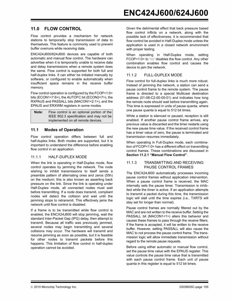
ENC424J600/624J600
11.0 FLOW CONTROL
Flow control provides a mechanism for networkstations to temporarily stop transmission of data tothemselves. This feature is commonly used to preventbuffer overruns while receiving data.
ENC424J600/624J600 devices are capable of bothautomatic and manual flow control. The hardware canadvertise when it is temporarily unable to receive dataand delay transmissions when a remote system doesthe same. Flow control is supported for both full andhalf-duplex links. It can either be initiated manually bysoftware, or configured to enable automatically wheninsufficient space remains in the receive buffermemory.
Flow control operation is configured by the FCOP<1:0>bits (ECON1<7:6>), the AUTOFC bit (ECON2<7>), theRXPAUS and PASSALL bits (MACON1<2:1>), and theEPAUS and ERXWM registers in some modes.
11.1 Modes of Operation
Flow control operation differs between full andhalf-duplex links. Both modes are supported, but it isimportant to understand the difference before enablingflow control in an application.
11.1.1 HALF-DUPLEX MODE
When the link is operating in Half-Duplex mode, flowcontrol operates by jamming the network. The nodewishing to inhibit transmissions to itself sends apreamble pattern of alternating ones and zeros (55h)on the medium; this is also known as asserting backpressure on the link. Since the link is operating underHalf-Duplex mode, all connected nodes must waitbefore transmitting. If a node does transmit, compliantnodes will detect the collision and wait until thejamming stops to retransmit. This effectively jams thenetwork until flow control is disabled.
If a frame is to be transmitted while flow control isenabled, the ENCX24J600 will stop jamming, wait thestandard Inter-Packet Gap (IPG) delay, then attempt totransmit. Because all traffic was previously jammed,several nodes may begin transmitting and severalcollisions may occur. The hardware will transmit andresume jamming as soon as possible, but it is feasiblefor other nodes to transmit packets before thishappens. This limitation of flow control in half-duplexoperation cannot be avoided.
Given the detrimental effect that back pressure basedflow control inflicts on a network, along with thepossible lack of effectiveness, it is recommended thatflow control be avoided in Half-Duplex mode unless theapplication is used in a closed network environmentwith proper testing.
When operating in Half-Duplex mode, settingFCOP<1:0> to ‘00’ disables the flow control. Any othercombination enables flow control and causes thedevice to jam the network.
11.1.2 FULL-DUPLEX MODE
Flow control for full-duplex links is much more robust.Instead of jamming the network, a station can send apause control frame to the remote system. The pauseframe is directed to a special Multicast destinationaddress (01-08-C2-00-00-01) and indicates how longthe remote node should wait before transmitting again.This time is expressed in units of pause quanta, whereone pause quanta is equal to 512 bit times.
While a station is silenced or paused, reception is stillenabled. If another pause control frame arrives, anyprevious value is discarded and the timer restarts usingthe new pause time value. If the received control framehas a timer value of zero, the pause is terminated andtransmission resumes immediately.
When operating in Full-Duplex mode, each combina-tion of FCOP<1:0> has a different effect on transmittingcontrol frames. These combinations are discussed inSection 11.2.1 “Manual Flow Control”.
11.1.3 TRANSMITTING AND RECEIVING PAUSE CONTROL FRAMES
The ENCX24J600 automatically processes incomingpause control frames without application intervention.When a pause control frame is received, the MACinternally sets the pause timer. Transmission is inhib-ited while the timer is active. If an application attemptsto transmit a packet during this time, the transmissionlogic will stall until the time expires (i.e., TXRTS willstay set for longer than normal).
Pause control frames are normally filtered out by theMAC and are not written to the receive buffer. Setting thePASSALL bit (MACON1<1>) alters this behavior andcauses these frames to pass through the receive filters.If the frame is accepted, it will be written to the receivebuffer. However, setting PASSALL will also cause theMAC to not process the pause control frame. The trans-mission logic will allow immediate transmission withoutregard to the remote pause requests.
Before using either automatic or manual flow control,set the pause time value with the EPAUS register. Thisvalue controls the pause time value that is transmittedwith each pause control frame. Each unit of pausequanta in this register is equal to 512 bit times.
Note: Flow control is an optional portion of theIEEE 802.3 specification and may not beimplemented on all remote devices.
2010 Microchip Technology Inc. DS39935C-page 105

ENC424J600/624J600
11.2 Manual and Automatic Flow Control
11.2.1 MANUAL FLOW CONTROL
Manual flow control is enabled by default on devicepower-up and whenever the AUTOFC bit (ECON2<7>)is cleared. Setting AUTOFC disables manual flowcontrol.
To begin manual flow control in Full-Duplex mode, setFCOP<1:0> to one of the following combinations:
• Idle (‘00’): Flow control is disabled or Idle.
• Single Pause (‘01’): Transmit one pause frame for the time indicated in EPAUS; automatically returns to the Idle state (‘00’).
• Continuous Pause (‘10’): Periodically transmit pause frames using the value indicated in EPAUS for an indefinite time; must be terminated using End (‘11’).
• End (‘11’): Transmit one pause frame with a timer of 0000h, then return to the Idle state (‘00’).
In Half-Duplex mode, set FCOP<1:0> to ‘10’ to beginflow control and to ‘00’ to terminate flow control.
11.2.2 AUTOMATIC FLOW CONTROL
When the AUTOFC bit is set, the ENCX24J600 auto-matically initiates flow control operation when theamount of data in the receive buffer crosses an upperthreshold value. Flow control automatically terminatesonce the amount of pending data shrinks below a lowerthreshold. These thresholds, or “watermarks”, aredetermined by the upper and lower bytes (respectively)of the Receive Watermark register, ERXWM. Thesethresholds represent 96-byte blocks.
For example, setting the RXFWM bits to 20h and theRXEWM bits to 10h initiates flow control when morethan 3072 bytes of data are present in the buffer. Flowcontrol terminates when fewer than 1536 bytes of dataare in the buffer.
In Automatic mode, the value of FCOP<1:0> iscontrolled by the device and must not be changed bysoftware. These bits, however, can be used as statusbits to determine what state the automatic flow controlengine is in. A value of ‘10’ indicates flow control isactive, while ‘00’ indicates that flow control is Idle.
To use automatic flow control:
1. Set the EPAUS register to indicate how manypause quanta should be specified in eachcontrol frame. It is recommended that the defaultvalue be used.
2. Set RXFWM<7:0> (ERXWM<15:8>) to indicatewhen flow control is to begin. When this numberof 96-byte blocks is consumed in the receivebuffer, the device considers its receive buffer tobe full and initiates flow control. Use the defaultvalue of 16 if the full threshold is to be set at1536 bytes.
3. Set RXEWM<7:0> (ERXWM<7:0>) to indicatewhen flow control is to end. When the number ofoccupied 96-byte blocks falls below this level,the device considers its receive buffer to beempty enough to receive more data. Use thedefault value of 15 if the empty threshold is to beset at 1440 bytes.
4. Set AUTOFC (ECON2<7>) to give control of theFCOP<1:0> bits to the automatic flow controlhardware.
Note: When flow control is used in conjunctionwith auto-negotiation, also set the ADPAUSbits (PHANA<11:10>) to ‘01’ during initial-ization. See Section 12.0 “Speed/DuplexConfiguration and Auto-Negotiation” formore information.
Note: Setting RXFWM to be equal to RXEWM(i.e., no hysteresis between full and empty)is not permitted. For automatic flow controlto operate correctly, RXEWM must alwaysbe at least one less than RXFWM, implyingat least 96 bytes of hysteresis.
DS39935C-page 106 2010 Microchip Technology Inc.

ENC424J600/624J600
REGISTER 11-1: MACON1: MAC CONTROL REGISTER 1
R/W-x R/W-0 U-0 U-0 R/W-0 R/W-0 R/W-0 R/W-0
r r — — r r r r
bit 15 bit 8
U-0 U-0 U-0 R/W-0 R/W-1 R/W-1 R/W-0 R/W-1
— — — LOOPBK r RXPAUS PASSALL r
bit 7 bit 0
Legend:
R = Readable bit W = Writable bit U = Unimplemented bit, read as ‘0’
-n = Value at POR ‘1’ = Bit is set ‘0’ = Bit is cleared x = Bit is unknown
bit 15-14 Reserved: Write as ‘0’
bit 13-12 Unimplemented: Read as ‘0’
bit 11-8 Reserved: Write as ‘0’
bit 7-5 Unimplemented: Read as ‘0’
bit 4 LOOPBK: MAC Loopback Enable bit
1 = Transmitted packets are looped back inside the MAC before reaching the PHY0 = Normal operation
bit 3 Reserved: Write as ‘1’
bit 2 RXPAUS: Pause Control Frame Reception Enable bit
1 = Inhibit transmissions when pause control frames are received (normal operation)0 = Ignore pause control frames which are received
bit 1 PASSALL: Pass All Received Frames Enable bit
1 = Control frames received by the MAC are written into the receive buffer if not filtered out0 = Control frames are discarded after being processed by the MAC (normal operation)
bit 0 Reserved: Write as ‘1’
2010 Microchip Technology Inc. DS39935C-page 107

ENC424J600/624J600
NOTES:
DS39935C-page 108 2010 Microchip Technology Inc.

ENC424J600/624J600
12.0 SPEED/DUPLEX CONFIGURATION AND AUTO-NEGOTIATION
ENC424J600/624J600 devices are capable of operationat 10Base-T and 100Base-TX speeds in Half-Duplexand Full-Duplex modes for each. The speed and Duplexmode can be selected manually, or the part can beconfigured to automatically select the optimum linkparameters based on the capabilities of the link partner.When operating in 10Base-T mode, the part alsocompensates for incorrect polarity on the TPIN+/- pins(100Base-TX signalling is non-polarized).
In half-duplex operation, only one Ethernet controllermay transmit on the physical medium at any given time.If the host controller initiates a transmission whileanother device is transmitting, the ENCX24J600 willdelay until the remote transmitter finishes its packet.Other devices on the medium should do the same whilethe ENCX24J600 is transmitting. If two controllersbegin transmitting at about the same time, a collisionwill occur. In this case, the data on the medium iscorrupt; the ENCX24J600 aborts transmission andattempts to retransmit later.
In full-duplex operation, both nodes may transmitsimultaneously, so collisions do not occur. For detailsabout transmitting packets, including collision detectionand correction, refer to Section 9.1 “TransmittingPackets”.
Speed and Duplex modes are configured in thePHCON1 register (Register 12-1). The PHSTAT1,PHSTAT2 and PHSTAT3 registers (Registers 12-2through 12-4) provide additional information about thestatus of the link. The PHANA, PHANLPA and PHANEregisters (Registers 12-5 through 12-7) containinformation about auto-negotiation status andconfiguration.
12.1 Manual Configuration
Speed and Duplex modes can be manually selected bydisabling auto-negotiation. Manual configuration isenabled by clearing the ANEN bit (PHCON1<12>).
When manual configuration is used, both the Speedand Duplex mode must be selected. Set the SPD100bit (PHCON1<13>) to select 100Base-TX operation orclear SPD100 to select 10Base-T mode. Set thePFULDPX bit (PHCON1<8>) to configure Full-Duplexmode or clear PFULDPX to use half-duplex operation.
After reconfiguring the Speed and Duplex modes,update the MACON2, MACLCON, MAIPG andMABBIPG registers as described in Section 8.9 “AfterLink Establishment”.
12.2 Auto-Negotiation
Auto-negotiation allows Ethernet devices to agreeupon the fastest supported transmission rate. When anEthernet link is broken, a series of Fast Link Pulses(FLPs) are transmitted periodically to initiate a link.Among other things, these pulses encode informationabout the node’s speed and duplex capabilities.
If a remote partner exists and supports auto-negotiation,it will reply with a burst of FLPs to advertise its own linkcapabilities. If both devices support 100Base-TX fullduplex, the link will be established and that mode will beused. Otherwise, the link falls back to 100Base-TX halfduplex, 10Base-T full duplex or 10Base-T half duplex, inthat order.
If the remote link partner does not support auto-negotiation, the device will use an algorithm known asParallel Detection to determine if the link partner is a10Base-T device or 100Base-TX device. ParallelDetection will optimally resolve the operating speed,however, it will not have any means of learning theduplex state of the remote node. Therefore, theENCX24J600 PHY will always resort to the half-duplexstate when auto-negotiation is not available. A duplexmismatch will occur if the remote device is operating inFull-Duplex mode. To determine whether or not theremote link supports auto-negotiation, check the valueof the LPANABL bit (PHANE<0>).
Auto-negotiation is enabled by default at power-up, butcan be disabled by clearing the ANEN bit. To restart theauto-negotiation process, set RENEG (PHCON1<9>).After setting RENEG, the hardware automatically clearsthis bit to ‘0’ immediately.
During auto-negation, the information in the PHANAregister is advertised to the link partner by transmittingthe information encoded in the Fast Link Pulses. TheANDONE bit (PHSTAT1<5>) is set by the hardwarewhen the auto-negotiation process completes. Thevalue of SPDDPX<2:0> (PHSTAT3<4:2>) indicateswhich operation mode has been selected. The remotelink partner’s capabilities are also stored in thePHANLPA register.
Note: When auto-negotiation is enabled,SPD100 (PHCON1<13>) and PFULDPX(PHCON1<8>) are control only bits. Theyhave no effect on Speed or Duplex modesand do not indicate the current selectionwhen read.
2010 Microchip Technology Inc. DS39935C-page 109

ENC424J600/624J600
When LINKIF link status change interrupt flag is set, itmeans auto-negotiation or parallel detection iscomplete. Once auto-negotiation is complete, the MACregisters related to Duplex mode must be reconfigured.Determine the new Duplex mode by reading thePHYDPX bit (ESTAT<10>). Once this is done, update
the MACON2, MACLCON, MAIPG and MABBIPGregisters as described in Section 8.9 “After LinkEstablishment”.
REGISTER 12-1: PHCON1: PHY CONTROL REGISTER 1
R/W-0 R/W-0 R/W-0 R/W-1 R/W-0 R/W-0 R/W-0 R/W-0
PRST PLOOPBK SPD100(1) ANEN PSLEEP r RENEG PFULDPX(1)
bit 15 bit 8
R/W-0 R-0 R-0 R-0 R-0 R-0 R-0 R-0
r r r r r r r r
bit 7 bit 0
Legend:
R = Readable bit W = Writable bit U = Unimplemented bit, read as ‘0’
-n = Value at POR ‘1’ = Bit is set ‘0’ = Bit is cleared x = Bit is unknown
bit 15 PRST: PHY Reset bit
1 = Perform PHY Reset. Hardware automatically clears this bit to ‘0’ when the Reset is complete.0 = PHY is not in Reset (normal operation)
bit 14 PLOOPBK: PHY Loopback Enable bit
1 = Loopback is enabled0 = Normal operation
bit 13 SPD100: PHY Speed Select Control bit(1)
1 = 100 Mbps0 = 10 Mbps
bit 12 ANEN: PHY Auto-Negotiation Enable bit
1 = Auto-negotiation is enabled. SPD100 and PFULDPX are ignored.0 = Auto-negotiation is disabled. SPD100 and PFULDPX control the operating speed and duplex.
bit 11 PSLEEP: PHY Sleep Enable bit
1 = PHY is powered down0 = Normal operation
bit 10 Reserved: Write as ‘0’, ignore on read
bit 9 RENEG: Restart Auto-Negotiation Control bit
1 = Restart the auto-negotiation process. Hardware automatically clears this bit to ‘0’ when the auto-negotiation process starts.
0 = Normal operation
bit 8 PFULDPX: PHY Duplex Select Control bit(1)
1 = Full duplex0 = Half duplex
bit 7 Reserved: Write as ‘0’, ignore on read
bit 6-0 Reserved: Ignore on read
Note 1: Applicable only when auto-negotiation is disabled (ANEN = 0).
DS39935C-page 110 2010 Microchip Technology Inc.

ENC424J600/624J600
REGISTER 12-2: PHSTAT1: PHY STATUS REGISTER 1
R-0 R-1(1) R-1(1) R-1(1) R-1(1) R-0 R-0 R-0
r FULL100 HALF100 FULL10 HALF10 r r r
bit 15 bit 8
R-0 R-0 R-0 R/LH-0 R-1(1) R/LL-0 R-0 R-1(1)
r r ANDONE LRFAULT ANABLE LLSTAT r EXTREGS
bit 7 bit 0
Legend: LL = Latch Low bit U = Unimplemented bit, read as ‘0’
R = Readable bit W = Writable bit LH = Latch High bit LL = Latch-Low bit
-n = Value at POR ‘1’ = Bit is set ‘0’ = Bit is cleared x = Bit is unknown
bit 15 Reserved: Read as ‘0’
bit 14 FULL100: 100Base-TX Full-Duplex Ability Status bit
1 = PHY is capable of 100Base-TX full-duplex operation(1)
bit 13 HALF100: 100Base-TX Half-Duplex Ability Status bit
1 = PHY is capable of 100Base-TX half-duplex operation(1)
bit 12 FULL10: 10Base-T Full-Duplex Ability Status bit
1 = PHY is capable of 10Base-T full-duplex operation(1)
bit 11 HALF10: 10Base-T Half-Duplex Ability Status bit
1 = PHY is capable of 10Base-T half-duplex operation(1)
bit 10-6 Reserved: Ignore on read
bit 5 ANDONE: Auto-Negotiation Done Status bit
1 = Auto-negotiation is complete0 = Auto-negotiation is disabled or still in progress
bit 4 LRFAULT: Latching Remote Fault Condition Status bit
1 = Remote Fault condition has been detected. This bit latches high and automatically returns to ‘0’after PHSTAT1 is read.
0 = No remote Fault has been detected since the last read of PHSTAT1
bit 3 ANABLE: Auto-Negotiation Ability Status bit
1 = PHY is capable of auto-negotiation(1)
bit 2 LLSTAT: Latching Link Status bit
1 = Ethernet link is established and has stayed continuously established since the last read ofPHSTAT1
0 = Ethernet link is not established or was not established for a period since the last read of PHSTAT1
bit 1 Reserved: Ignore on read
bit 0 EXTREGS: Extended Capabilities Registers Present Status bit
1 = PHY has extended capability registers at addresses, 16 thru 31(1)
Note 1: This is the only valid state for this bit; a ‘0’ represents an invalid condition.
2010 Microchip Technology Inc. DS39935C-page 111
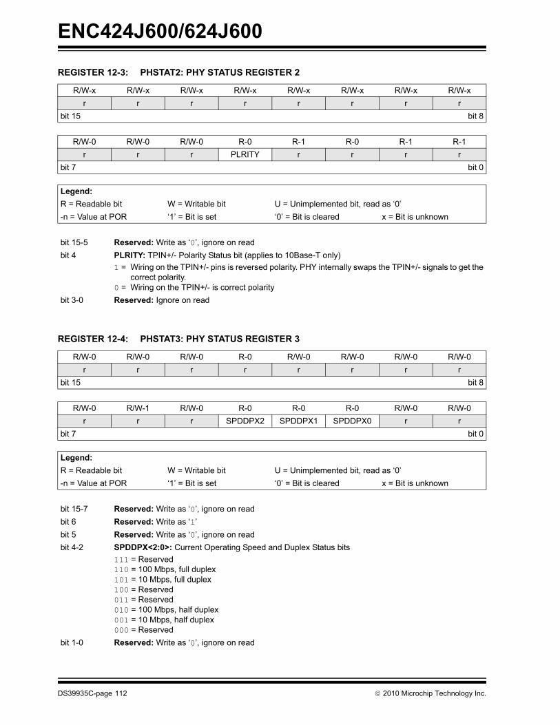
ENC424J600/624J600
REGISTER 12-3: PHSTAT2: PHY STATUS REGISTER 2
R/W-x R/W-x R/W-x R/W-x R/W-x R/W-x R/W-x R/W-x
r r r r r r r r
bit 15 bit 8
R/W-0 R/W-0 R/W-0 R-0 R-1 R-0 R-1 R-1
r r r PLRITY r r r r
bit 7 bit 0
Legend:
R = Readable bit W = Writable bit U = Unimplemented bit, read as ‘0’
-n = Value at POR ‘1’ = Bit is set ‘0’ = Bit is cleared x = Bit is unknown
bit 15-5 Reserved: Write as ‘0’, ignore on read
bit 4 PLRITY: TPIN+/- Polarity Status bit (applies to 10Base-T only)
1 = Wiring on the TPIN+/- pins is reversed polarity. PHY internally swaps the TPIN+/- signals to get thecorrect polarity.
0 = Wiring on the TPIN+/- is correct polarity
bit 3-0 Reserved: Ignore on read
REGISTER 12-4: PHSTAT3: PHY STATUS REGISTER 3
R/W-0 R/W-0 R/W-0 R-0 R/W-0 R/W-0 R/W-0 R/W-0
r r r r r r r r
bit 15 bit 8
R/W-0 R/W-1 R/W-0 R-0 R-0 R-0 R/W-0 R/W-0
r r r SPDDPX2 SPDDPX1 SPDDPX0 r r
bit 7 bit 0
Legend:
R = Readable bit W = Writable bit U = Unimplemented bit, read as ‘0’
-n = Value at POR ‘1’ = Bit is set ‘0’ = Bit is cleared x = Bit is unknown
bit 15-7 Reserved: Write as ‘0’, ignore on read
bit 6 Reserved: Write as ‘1’
bit 5 Reserved: Write as ‘0’, ignore on read
bit 4-2 SPDDPX<2:0>: Current Operating Speed and Duplex Status bits
111 = Reserved110 = 100 Mbps, full duplex101 = 10 Mbps, full duplex100 = Reserved011 = Reserved010 = 100 Mbps, half duplex001 = 10 Mbps, half duplex000 = Reserved
bit 1-0 Reserved: Write as ‘0’, ignore on read
DS39935C-page 112 2010 Microchip Technology Inc.

ENC424J600/624J600
REGISTER 12-5: PHANA: PHY AUTO-NEGOTIATION ADVERTISEMENT REGISTER
R-0 R-0 R/W-0 R-0 R/W-0 R/W-0 R-0 R/W-1
ADNP r ADFAULT r ADPAUS1 ADPAUS0 r AD100FD
bit 15 bit 8
R/W-1 R/W-1 R/W-1 R/W-0 R/W-0 R/W-0 R/W-0 R/W-1
AD100 AD10FD AD10 ADIEEE4 ADIEEE3 ADIEEE2 ADIEEE1 ADIEEE0
bit 7 bit 0
Legend:
R = Readable bit W = Writable bit U = Unimplemented bit, read as ‘0’
-n = Value at POR ‘1’ = Bit is set ‘0’ = Bit is cleared x = Bit is unknown
bit 15 ADNP: Advertise Next Page Ability bit
1 = Invalid0 = Local PHY does not support auto-negotiation next page abilities
bit 14 Reserved: Read as ‘0’
bit 13 ADFAULT: Advertise Remote Fault Condition bit
1 = Local PHY has a Fault condition present0 = Local PHY does not have a Fault condition present
bit 12 Reserved: Read as ‘0’
bit 11-10 ADPAUS<1:0>: Advertise PAUSE Flow Control Ability bits
11 = Local device supports both symmetric PAUSE and asymmetric PAUSE toward local device10 = Local device supports asymmetric PAUSE toward link partner only01 = Local device supports symmetric PAUSE only (Normal Flow Control mode)00 = Local device does not support PAUSE flow control
bit 9 Reserved: Read as ‘0’
bit 8 AD100FD: Advertise 100Base-TX Full-Duplex Ability bit
1 = Local PHY is capable of 100Base-TX full-duplex operation0 = Local PHY is incapable of 100Base-TX full-duplex operation
bit 7 AD100: Advertise 100Base-TX Half-Duplex Ability bit
1 = Local PHY is capable of 100Base-TX half-duplex operation0 = Local PHY is incapable of 100Base-TX half-duplex operation
bit 6 AD10FD: Advertise 10Base-T Full-Duplex Ability bit
1 = Local PHY is capable of 10Base-T full-duplex operation0 = Local PHY is incapable of 10Base-T full-duplex operation
bit 5 AD10: Advertise 10Base-T Half-Duplex Ability bit
1 = Local PHY is capable of 10Base-T half-duplex operation0 = Local PHY is incapable of 10Base-T half-duplex operation
bit 4-0 ADIEEE<4:0>: Advertise IEEE Standard Selector Field bits
00001 = IEEE 802.3 Std.All other values reserved by IEEE. Always specify a selector value of ‘00001’ for this device.
2010 Microchip Technology Inc. DS39935C-page 113

ENC424J600/624J600
REGISTER 12-6: PHANLPA: PHY AUTO-NEGOTIATION LINK PARTNER ABILITY REGISTER
R-0 R-0 R-0 R-0 R-0 R-0 R-0 R-0
LPNP LPACK LPFAULT r LPPAUS1 LPPAUS0 LP100T4 LP100FD
bit 15 bit 8
R-0 R-0 R-0 R-0 R-0 R-0 R-0 R-0
LP100 LP10FD LP10 LPIEEE4 LPIEEE3 LPIEEE2 LPIEEE1 LPIEEE0
bit 7 bit 0
Legend:
R = Readable bit W = Writable bit U = Unimplemented bit, read as ‘0’
-n = Value at POR ‘1’ = Bit is set ‘0’ = Bit is cleared x = Bit is unknown
bit 15 LPNP: Link Partner Next Page Ability bit
1 = Link partner PHY supports auto-negotiation next page abilities0 = Link partner PHY does not support auto-negotiation next page abilities
bit 14 LPACK: Link Partner Acknowledge Local PHY Code Word Status bit
1 = Link partner PHY has successfully received the local PHY abilities saved in PHANA0 = Link partner PHY has not received the local PHY abilities saved in PHANA
bit 13 LPFAULT: Link Partner Remote Fault Condition bit
1 = Link partner PHY has a Fault condition present0 = Link partner PHY does not have a Fault condition present
bit 12 Reserved: Ignore on read
bit 11-10 LPPAUS<1:0>: Link Partner PAUSE Flow Control Ability bits
11 = Link partner supports both symmetric PAUSE and asymmetric PAUSE toward local device. Linkpartner generates and responds to PAUSE control frames. Alternatively, if the local device onlysupports asymmetric PAUSE, the link partner will respond to PAUSE control frames, but notgenerate any.
10 = Link partner supports asymmetric PAUSE toward local device only; it can transmit PAUSE controlframes, but cannot act upon PAUSE frames sent to it
01 = Link partner supports symmetric PAUSE only, and generates and responds to PAUSE controlframes
00 = Link partner does not support PAUSE flow control
bit 9 LP100T4: Link Partner 100Base-T4 Ability bit
1 = Link partner PHY is capable of operating in 100Base-T4 mode0 = Link partner PHY is incapable of operating in 100Base-T4 mode
bit 8 LP100FD: Link Partner 100Base-TX Full-Duplex Ability bit
1 = Link partner PHY is capable of 100Base-TX full-duplex operation0 = Link partner PHY is incapable of 100Base-TX full-duplex operation
bit 7 LP100: Link Partner 100Base-TX Half-Duplex Ability bit
1 = Link partner PHY is capable of 100Base-TX half-duplex operation0 = Link partner PHY is incapable of 100Base-TX half-duplex operation
bit 6 LP10FD: Link Partner 10Base-T Full-Duplex Ability bit
1 = Link partner PHY is capable of 10Base-T full-duplex operation0 = Link partner PHY is incapable of 10Base-T full-duplex operation
bit 5 LP10: Link Partner 10Base-T Half-Duplex Ability bit
1 = Link partner PHY is capable of 10Base-T half-duplex operation0 = Link partner PHY is incapable of 10Base-T half-duplex operation
bit 4-0 LPIEEE<4:0>: Link Partner IEEE Standard Selector Field bits
00001 = IEEE 802.3 Std.All other values are reserved by IEEE. Remote node should also specify this as the selector value.
DS39935C-page 114 2010 Microchip Technology Inc.

ENC424J600/624J600
REGISTER 12-7: PHANE: PHY AUTO-NEGOTIATION EXPANSION REGISTER
R-0 R-0 R-0 R-0 R-0 R-0 R-0 R-0
r r r r r r r r
bit 15 bit 8
R-0 R-0 R-0 R/LH-0 R-0 R-0 R/LH-0 R-0
r r r PDFLT r r LPARCD LPANABL
bit 7 bit 0
Legend: LH = Latch High bit
R = Readable bit W = Writable bit U = Unimplemented bit, read as ‘0’
-n = Value at POR ‘1’ = Bit is set ‘0’ = Bit is cleared x = Bit is unknown
bit 15-5 Reserved: Ignore on read
bit 4 PDFLT: Parallel Detection Fault Status bit
1 = Parallel detection did not detect a valid link partner; automatically cleared when register is read0 = Parallel detection is still in progress or a valid link partner is connected
bit 3-2 Reserved: Ignore on read
bit 1 LPARCD: Link Partner Abilities Received Status bit
1 = PHANLPA register has been written with a new value from the link partner; automatically clearedwhen register is read
0 = PHANLPA contents have not changed since the last read of PHANE
bit 0 LPANABL: Link Partner Auto-Negotiation Able Status bit
1 = Link partner implements auto-negotiation0 = Link partner does not implement auto-negotiation
2010 Microchip Technology Inc. DS39935C-page 115

ENC424J600/624J600
NOTES:
DS39935C-page 116 2010 Microchip Technology Inc.
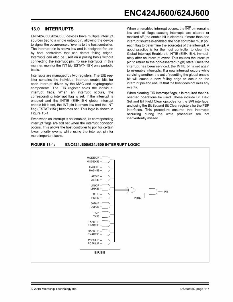
ENC424J600/624J600
13.0 INTERRUPTS
ENC424J600/624J600 devices have multiple interruptsources tied to a single output pin, allowing the deviceto signal the occurrence of events to the host controller.The interrupt pin is active-low and is designed for useby host controllers that can detect falling edges.Interrupts can also be used on a polling basis withoutconnecting the interrupt pin. To use interrupts in thismanner, monitor the INT bit (ESTAT<15>) on a periodicbasis.
Interrupts are managed by two registers. The EIE reg-ister contains the individual interrupt enable bits foreach interrupt driven by the MAC and cryptographiccomponents. The EIR register holds the individualinterrupt flags. When an interrupt occurs, thecorresponding interrupt flag is set. If the interrupt isenabled and the INTIE (EIE<15>) global interruptenable bit is set, the INT pin is driven low and the INTflag (ESTAT<15>) becomes set. This logic is shown inFigure 13-1.
Even when an interrupt is not enabled, its correspondinginterrupt flags are still set when the interrupt conditionoccurs. This allows the host controller to poll for certainlower priority events while using the interrupt pin formore important tasks.
When an enabled interrupt occurs, the INT pin remainslow until all flags causing interrupts are cleared ormasked off (the enable bit is cleared). If more than oneinterrupt source is enabled, the host controller must polleach flag to determine the source(s) of the interrupt. Agood practice is for the host controller to clear theGlobal Interrupt Enable bit, INTIE (EIE<15>), immedi-ately after an interrupt event. This causes the interruptpin to return to the non-asserted (high) state. Once theinterrupt has been serviced, the INTIE bit is set againto re-enable interrupts. If a new interrupt occurs whileservicing another, the act of resetting the global enablebit will cause a new falling edge to occur on theinterrupt pin and ensure that the host does not miss anyevents.
When clearing EIR interrupt flags, it is required that bit-oriented operations be used. These include Bit FieldSet and Bit Field Clear opcodes for the SPI interface,and using the Bit Set and Bit Clear registers for the PSPinterfaces. This procedure ensures that interruptsoccurring during the write procedure are notinadvertently missed.
FIGURE 13-1: ENC424J600/624J600 INTERRUPT LOGIC
INT
INTIE
LINKIELINKIF
AESIEAESIF
HASHIEHASHIF
MODEXIE
MODEXIF
EIR/EIE
RXABTIERXABTIF
TXABTIETXABTIF
TXIETXIF
DMAIEDMAIF
PKTIE
PKTIF
PCFULIEPCFULIF
2010 Microchip Technology Inc. DS39935C-page 117

ENC424J600/624J600
REGISTER 13-1: EIR: ETHERNET INTERRUPT FLAG REGISTER
R/W-0 R/W-0 R/W-0 R/W-0 R/W-1 R/W-0 R/W-1 R/W-0
CRYPTEN MODEXIF HASHIF AESIF LINKIF r r r
bit 15 bit 8
R/W-0 R-0 R/W-0 R-0 R/W-0 R/W-0 R/W-0 R/W-0
r PKTIF DMAIF r TXIF TXABTIF RXABTIF PCFULIF
bit 7 bit 0
Legend:
R = Readable bit W = Writable bit U = Unimplemented bit, read as ‘0’
-n = Value at POR ‘1’ = Bit is set ‘0’ = Bit is cleared x = Bit is unknown
bit 15 CRYPTEN: Modular Exponentiation and AES Cryptographic Modules Enable bit
1 = All cryptographic engine modules are enabled0 = Modular exponentiation and AES modules are disabled and powered down; MD5/SHA-1 hashing
is still available
bit 14 MODEXIF: Modular Exponentiation Interrupt Flag bit
1 = Modular exponentiation calculation is complete0 = No interrupt pending
bit 13 HASHIF: MD5/SHA-1 Hash Interrupt Flag bit
1 = MD5/SHA-1 hash operation is complete0 = No interrupt pending
bit 12 AESIF: AES Encrypt/Decrypt Interrupt Flag bit
1 = AES encrypt/decrypt operation is complete0 = No interrupt pending
bit 11 LINKIF: PHY Link Status Change Interrupt Flag bit
1 = PHY Ethernet link status has changed. Read PHYLNK (ESTAT<8>) to determine the current state.0 = No interrupt pending
bit 10-7 Reserved: Ignore on read, don’t care on write
bit 6 PKTIF: RX Packet Pending Interrupt Flag bit
1 = One or more RX packets have been saved and are ready for software processing. ThePKTCNT<7:0> (ESTAT<7:0>) bits are non-zero. To clear this flag, decrement the PKTCNT bits tozero by setting PKTDEC (ECON1<8>).
0 = No RX packets are pending
bit 5 DMAIF: DMA Interrupt Flag bit
1 = DMA copy or checksum operation is complete0 = No interrupt pending
bit 4 Reserved: Ignore on read, don’t care on write
bit 3 TXIF: Transmit Done Interrupt Flag bit
1 = Packet transmission has completed. TXRTS (ECON1<1>) has been cleared by hardware.0 = No interrupt pending
bit 2 TXABTIF: Transmit Abort Interrupt Flag bit
1 = Packet transmission has been aborted due to an error. Read the ETXSTAT register to determinethe cause. TXRTS (ECON1<1>) has been cleared by hardware.
0 = No interrupt pending
DS39935C-page 118 2010 Microchip Technology Inc.

ENC424J600/624J600
bit 1 RXABTIF: Receive Abort Interrupt Flag bit
1 = An RX packet was dropped because there is insufficient space in the RX buffer to store thecomplete packet or the PKTCNT field is saturated at FFh
0 = No interrupt pending
bit 0 PCFULIF: Packet Counter Full Interrupt Flag bit
1 = PKTCNT field has reached FFh. Software must decrement the packet counter to prevent the nextRX packet from being dropped.
0 = No interrupt pending
REGISTER 13-1: EIR: ETHERNET INTERRUPT FLAG REGISTER (CONTINUED)
2010 Microchip Technology Inc. DS39935C-page 119

ENC424J600/624J600
REGISTER 13-2: EIE: ETHERNET INTERRUPT ENABLE REGISTER
R/W-1 R/W-0 R/W-0 R/W-0 R/W-0 R/W-0 R/W-0 R/W-0
INTIE MODEXIE HASHIE AESIE LINKIE r r r
bit 15 bit 8
R/W-0 R/W-0 R/W-0 R-1 R/W-0 R/W-0 R/W-0 R/W-0
r PKTIE DMAIE r(1) TXIE TXABTIE RXABTIE PCFULIE
bit 7 bit 0
Legend:
R = Readable bit W = Writable bit U = Unimplemented bit, read as ‘0’
-n = Value at POR ‘1’ = Bit is set ‘0’ = Bit is cleared x = Bit is unknown
bit 15 INTIE: INT Global Interrupt Enable bit1 = INT pin is controlled by the INT status bit (ESTAT<15>)0 = INT pin is driven high
bit 14 MODEXIE: Modular Exponentiation Interrupt Enable bit1 = Enabled0 = Disabled
bit 13 HASHIE: MD5/SHA-1 Hash Interrupt Enable bit1 = Enabled0 = Disabled
bit 12 AESIE: AES Encrypt/Decrypt Interrupt Enable bit1 = Enabled0 = Disabled
bit 11 LINKIE: PHY Link Status Change Interrupt Enable bit1 = Enabled0 = Disabled
bit 10-7 Reserved: Write as ‘0’
bit 6 PKTIE: RX Packet Pending Interrupt Enable bit1 = Enabled0 = Disabled
bit 5 DMAIE: DMA Interrupt Enable bit1 = Enabled0 = Disabled
bit 4 Reserved: Ignore on read, don’t care on write(1)
bit 3 TXIE: Transmit Done Interrupt Enable bit1 = Enabled0 = Disabled
bit 2 TXABTIE: Transmit Abort Interrupt Enable bit1 = Enabled0 = Disabled
bit 1 RXABTIE: Receive Abort Interrupt Enable bit1 = Enabled0 = Disabled
bit 0 PCFULIE: Packet Counter Full Interrupt Enable bit1 = Enabled0 = Disabled
Note 1: This bit is read-only and cannot be cleared. Hardware does not modify it.
DS39935C-page 120 2010 Microchip Technology Inc.

ENC424J600/624J600
13.1 Interrupt Sources
ENC424J600/624J600 devices have multiple interruptsources, each individually selectable. The variousinterrupt sources are described in the following sections.
For any of the following interrupts to propagate out ofthe device, the INTIE (EIE<15>) global interrupt enablemust be set.
13.1.1 MODULAR EXPONENTIATION COMPLETE
The modular exponentiation complete interrupt occurswhen a modular exponentiation operation is com-pleted. This flag is set when MODEXST (ECON1<15>)is cleared. The interrupt should be cleared by softwareonce it has been serviced.
To enable the modular exponentiation completeinterrupt, set MODEXIE (EIE<14>).
For more information on the modular exponentiationfeature, refer to Section 15.1 “Modular Exponentiation”.
13.1.2 MD5/SHA-1 HASH COMPLETE
The MD5/SHA-1 hash complete interrupt occurs whenthe hashing module completes a block or calculation.The interrupt flag is required when using the hashingengine; therefore, the flag must be cleared by softwareafter the interrupt has been serviced.
To enable the MD5/SHA-1 complete interrupt, setHASHIE (EIE<13>).
For more information on the MD5/SHA-1 hashing feature,refer to Section 15.2 “MD5 and SHA-1 Hashing”.
13.1.3 AES COMPLETE
The Advanced Encryption Standard (AES) completeinterrupt occurs when a block has been encrypted ordecrypted using the AES engine. This flag is set whenAESST (ECON1<11>) is cleared. The interrupt shouldbe cleared by software once it has been serviced.
To enable the AES complete interrupt, set AESIE(EIE<12>).
For more information on the Advanced EncryptionStandard engine, refer to Section 15.3 “AdvancedEncryption Standard (AES)”.
13.1.4 LINK CHANGE
The link change interrupt occurs when the PHY linkstatus changes. This flag is set by hardware when a linkhas either been established or broken between thedevice and a remote Ethernet partner. The current linkstatus can be read from PHYLNK (ESTAT<8>). Theinterrupt should be cleared by software once it hasbeen serviced.
To enable the link change interrupt, set LINKIE(EIE<11>).
13.1.5 RECEIVED PACKET PENDING
The received packet pending interrupt occurs whenone or more frames have been received and are readyfor software processing. This flag is set when thePKTCNT<7:0> (ESTAT<7:0>) bits are non-zero. Thisinterrupt flag is read-only and will automatically clearwhen the PKTCNT bits are decremented to zero. Formore details about receiving and processing incomingframes, refer to Section 9.0 “Transmitting andReceiving Packets”.
To enable the received packet pending interrupt, setPKTIE (EIE<6>). The corresponding interrupt flag isPKTIF (EIR<6>).
13.1.6 DMA COMPLETE
The DMA complete interrupt occurs when a DMA oper-ation (either copy or checksum calculation) completes.This flag is set when DMAST (ECON1<5>) is cleared.The interrupt should be cleared by software once it hasbeen serviced.
To enable the DMA complete interrupt, set DMAIE(EIE<5>).
13.1.7 TRANSMIT COMPLETE
The transmit complete interrupt occurs when the trans-mission of a frame has ended (whether or not it wassuccessful). This flag is set when TXRTS (ECON1<1>)is cleared. The interrupt should be cleared by softwareonce it has been serviced.
To enable the transmit complete interrupt, set TXIE(EIE<3>).
2010 Microchip Technology Inc. DS39935C-page 121

ENC424J600/624J600
13.1.8 TRANSMIT ABORT
The transmit abort interrupt occurs when the transmis-sion of a frame has been aborted. An abort can occurfor any of the following reasons:
• Excessive collisions occurred as defined by the Retransmission Maximum, MAXRET<3:0> bits (MACLCON<3:0>), setting. If this occurs, the COLCNT bits (ETXSTAT<3:0>) will indicate the number of collisions that occurred.
• A late collision occurred after 63 bytes were trans-mitted. If this occurs, LATECOL (ETXSTAT<10>) will be set.
• The medium was busy and the packet was deferred. If this occurs, EXDEFER (ETXSTAT<8>) will be set.
• The application aborted the transmission by clearing TXRTS (ECON1<1>).
The interrupt should be cleared by software once it hasbeen serviced.
To enable the transmit abort interrupt, set TXABTIE(EIE<2>).
13.1.9 RECEIVE ABORT
The receive abort interrupt occurs when the receptionof a frame has been aborted. A frame being received isaborted when the Head Pointer attempts to overrun theTail Pointer, or when the packet counter has reachedFFh. In either case, the receive buffer is full and cannotfit the incoming frame, so the packet has beendropped. This interrupt does not occur when packetsare dropped due to the receive filters rejecting apacket. The interrupt should be cleared by softwareonce it has been serviced.
To enable the receive abort interrupt, set RXABTIE(EIE<1>). The corresponding interrupt flag is RXABTIF(EIR<1>).
13.1.10 RECEIVE PACKET COUNTER FULL
The receive packet counter full interrupt occurs whenthe PKTCNT (ESTAT<7:0>) bits have reached FFh.This indicates that the counter for received frames isfull and no more packets can be received. If a packetarrives after this flag is set, it will cause the receiveabort interrupt flag to be set. This flag is cleared byhardware once the PKTCNT bits are decremented.
To enable the receive packet counter full interrupt, setPCFULIE (EIE<0>).
13.2 Wake-on-LAN/Remote Wake-up
Wake-on-LAN or remote wake-up is useful for conserv-ing system power. The host controller and othersubsystems can be placed in Low-Power mode, thenconfigured to wake-up when a Magic Packet™ isreceived by the ENC424J600/624J600 devices.
For Wake-on-LAN to operate correctly, the device mustnot be in Low-Power mode and the receive modulemust be enabled. When a Magic Packet arrives, thedevice wakes the host controller via the INT signal.
To configure the device for Wake-on-LAN:
1. Set the host controller to wake-up on an externalinterrupt signal from INT.
2. Set CRCEN (ERXFCON<6>), RUNTEN(ERXFCON<4>) and MPEN (ERXFCON<14>).Clear all other filter enable bits. This configuresthe device to only accept Magic Packets.
3. Service all pending packets.
4. Set PKTIE (EIE<6>) and INTIE (EIE<15>) tointerrupt when a packet is accepted.
5. Put the host controller and other subsystems toSleep to save power.
Once a Magic Packet is received, PKTCNT is incre-mented to ‘1’, causing the device to assert the interruptsignal. When the host wakes up, it needs to restore thenormal filter configuration and continue performing itstasks.
For more details about the Magic Packet filter, refer toSection 10.10 “Magic Packet™ Collection Filter”.
DS39935C-page 122 2010 Microchip Technology Inc.

ENC424J600/624J600
14.0 DIRECT MEMORY ACCESS (DMA) CONTROLLER
ENC424J600/624J600 devices incorporate a DirectMemory Access (DMA) controller to reduce the burdenon the host processor. The module serves the followingpurposes:
• Copying data from one part of the packet buffer to another.
• Copying data between the packet buffer and one of the memory mapped cryptographic engines.
• Calculating a 16-bit checksum over a block of data, compatible with the checksum used in standard protocols, such as IP and TCP.
In general, the application configures the DMA opera-tion parameters (such as source and destinationaddresses), then sets the DMAST (ECON1<5>) bit tostart the transfer or calculation. The hardware auto-matically clears the bit when the operation finishes.Additionally, the module can be configured to set aninterrupt flag on completion, as detailed inSection 13.0 “Interrupts”.
The DMA module follows the same addresswrap-around logic as the indirect memory accessinterfaces described in Section 3.5.5 “Indirect SRAMBuffer Access”. When a read or write operationreaches the end of the User-Defined Area (UDA)specified by EUDAND, it automatically wraps toEUDAST. When an operation reaches the end of thegeneral purpose buffer, as indicated by ERXST – 1, itautomatically wraps to 0000h. Finally, when an opera-tion reaches the end of the receive buffer (the lastaddress in the physical memory space), it automaticallywraps to ERXST. If any of these areas share an endingaddress, the UDA wrapping will take priority, followedby the general purpose buffer wrapping, then thereceive buffer. The wrap-around applies to both thesource and destination addresses as an operationprogresses.
Although memory is organized by the 16-bit word, theDMA accepts any byte address as the source anddestination. It is also capable of operation over an evenor an odd number of bytes. Internally, the DMA uses16-bit accesses, so optimal efficiency is achieved whenboth the source and destination addresses are even, orwhen both are odd. Copy operations from an oddsource address to an even destination address or viceversa are allowed; however, performance will be dimin-ished by approximately 50% relative to copy operationon addresses that are aligned to each other.
It is recommended that DMA configuration parameters(such as address pointers and operation selection bits)not be modified while DMAST (ECON1<5>) is set andthe DMA is active. This requirement is additionally truefor the EUDAND Pointer, even if it is not located any-where within the source or destination memory rangesof the DMA. After processing each memory word, theDMA performs the necessary address wrap-aroundchecks to increment to the next address(es). If the hostcontroller writes to EUDAND at the exact moment theDMA is performing an address wrap-around check, it ispossible that the EUDAND register will be in atemporary incoherent state and the DMA source ordestination address will wrap to the EUDAST valueunintentionally.
Depending upon the operation and the alignment of thesource and destination addresses, the DMA moduletypically requires between one and three clock cyclesof OSC1 per 16-bit word. Any DMA operation inprogress can be cancelled by clearing the DMAST bit.
14.1 Copying Memory
The DMA can copy any length of data from any addressto any destination, including the corner case when thelength is zero. Source and destination addresses maybe within the implemented SRAM area (0000h through5FFFh) or the cryptographic data area (7800h through7C4Fh). It is not possible to use the DMA to read orwrite from SFRs.
Before initiating the first copy operation, verify that theETHEN (ECON2<15>) and CLKRDY (ESTAT<12>)bits are set. This does not need to be done forsubsequent operations.
To copy data from one location to another:
1. Verify that the values of ERXST, EUDAND andEUDAST (if applicable) are selecting thedesired buffer wrapping configuration.
2. Verify that DMAST (ECON1<5>) is clear,indicating that the module is Idle.
3. Set DMACPY (ECON1<4>) to select a copyoperation.
4. Optionally, set DMANOCS (ECON1<2>) toprevent a checksum calculation.
5. Set EDMAST to point to the source address.
6. Set EDMADST to point to the destinationaddress.
7. Set EDMALEN to indicate the number of bytesto copy.
8. Set DMAST to initiate the operation.
9. Wait for the hardware to clear DMAST to indicatecompletion. If the DMA interrupt is enabled, it willbe triggered when DMAST is cleared.
2010 Microchip Technology Inc. DS39935C-page 123

ENC424J600/624J600
Copy operations are performed starting with the firstbyte or word at the source address and incrementingforward. It is legal to use the DMA to move a block ofdata backwards in memory, even if the source anddestination memory ranges overlap. For example, if a65-byte packet of data was located starting at memoryaddress 0001h, and the application wished to move thewhole packet to address 0000h, it may simply programEDMAST to 0001h and EDMADST to 0000h. Thenon-overlapping byte at address 00041h will remainunchanged. Similarly, it is also legal to move a block ofdata from an even aligned address to an immediatelyprior odd aligned address. For example, moving from0002h to 0001h will work correctly with the finalnon-overlapping byte again remaining unchanged.Since copy operations start at the beginning of thesource address range and increment forward (asopposed to starting at the end of the source range andincrementing backwards), it is not possible to moveblocks of data forward towards a higher memoryaddress if the source and destination address rangesoverlap. To perform this operation, the application mustcopy the source data to a non-overlapping temporarybuffer location and then copy it from the temporarybuffer to the final destination.
14.2 Checksum Calculations
The DMA module can compute an IP checksum valueover a given range of bytes. Checksums can be calcu-lated over a specific range of memory, or simultaneouslyas a copy operation progresses. Remember to verifythat the values of ERXST, EUDAND and EUDAST (ifapplicable) are selecting the desired buffer wrappingconfiguration before starting any checksum operation.
The checksum calculation logic treats the source dataas a series of 16-bit big-endian integers. If the sourcedata has an odd number of bytes, a padding byte of 00hwill be added for the calculation. (This byte is notcopied to the destination if the checksum is part of acopy operation.) The calculated checksum is the 16-bitone’s complement of the one’s complement sum of all16-bit integers in the series. For example, if the bytesincluded in the checksum were 89h, ABh, CDh, thechecksum would begin by calculating 89ABh + CD00h.A carry would occur and the result would be 56ACh.That value would be complemented to yield achecksum of A953h.
To calculate a checksum without copying data:
1. Verify that DMAST (ECON1<5>) is clear,indicating that the module is Idle.
2. Clear DMACPY (ECON1<4>) to prevent a copyoperation.
3. Clear DMANOCS (ECON1<2>) to select achecksum calculation.
4. Clear DMACSSD (ECON1<3>) to use thedefault seed of 0000h. See the paragraph belowto seed a checksum with another value.
5. Set EDMAST to point to the source address.
6. Set EDMALEN to indicate the length of the inputdata.
7. Set DMAST to initiate the operation.8. Wait for the hardware to clear DMAST to indicate
completion. If the DMA interrupt is enabled, it willbe triggered when DMAST is cleared.
9. Read the computed checksum from EDMACS.
To calculate a checksum while copying data:
1. Verify that DMAST is clear, indicating that themodule is Idle.
2. Set DMACPY to select a copy operation.3. Clear DMANOCS to select a checksum
calculation.4. Clear DMACSSD to use the default seed of
0000h. See the paragraph below to seed achecksum with another value.
5. Set EDMAST to point to the source address.6. Set EDMADST to point to the destination
address.7. Set EDMALEN to indicate the number of bytes
to copy.8. Set DMAST to initiate the operation.9. Wait for the hardware to clear DMAST to indicate
completion. If the DMA interrupt is enabled, it willbe triggered when DMAST is cleared.
10. Read the computed checksum from EDMACS.
The checksum can be seeded with a previous value ifrequired. Seeding may be useful when attempting tocompute a checksum over non-contiguous blocks ofdata. To seed the checksum, set DMACSSD(ECON1<3>) before initiating the operation. Thechecksum calculation is seeded with the one’scomplement of the value contained in EDMACS prior tothe start of the DMA operation.
14.3 DMA Performance
The DMA controller can operate at any time, withoutany regard to other modules in the device. Severalfactors affect its speed of operation, including:
• Ethernet transmit and receive utilization, especially at 100 Mbps
• SPI or PSP read or write operations to the SRAM• Operating mode (copy versus checksum only)• Even-to-odd or odd-to-even source and
destination addresses (Copy mode)
Neglecting the time it takes software to program theDMA control SFRs, under typical unloaded conditions,the DMA will have a Checksum Only mode throughputof 100 Mbytes/second. Copy mode (with or withoutchecksum) will achieve a typical throughput of50 Mbytes/second when the source and destinationaddresses share the same alignment. Differing sourceand destination alignment would slow the process to33.3 Mbytes/second.
Worst case conditions can cut the DMA throughput byno more than half of the typical values.
DS39935C-page 124 2010 Microchip Technology Inc.

ENC424J600/624J600
15.0 CRYPTOGRAPHIC SECURITY ENGINES
To reduce the processing requirements of the hostcontroller, ENC424J600/624J600 devices incorporatethree different cryptographic security engines. Thesesecurity engines perform the types of encryptions,decryptions and mathematical computations that aremost commonly used for network security functions.They accelerate the computation of public/private keypair negotiations, message hash authentication andbulk data encryption.
The engines implemented are:
• Modular Exponentiation• MD5 and SHA-1 Hashing• Advanced Encryption Standard (AES)
Each engine operates from the cryptography datamemory area, shown in Section 3.4 “CryptographicData Memory”. This memory block is not directly acces-sible through the SPI or PSP interfaces. Instead, datamust be copied into this memory area using the DMA, asdescribed in Section 14.1 “Copying Memory”.
The modules are controlled using bits from the ECON2,ECON1 and EIR registers (Registers 8-1, 9-1 and 13-1,respectively). Each of the three modules have separateresources, so they may all be active simultaneously ifnecessary. Each module also has its own interrupt thatcan be enabled to signal completion. Refer toSection 13.0 “Interrupts” for details on using interrupts.
All of the cryptographic security engines require that theEthernet enable bit, ETHEN (ECON2<15>) to be set foroperation. However, the PHY, which consumes themajority of the device current, can be put to sleep if theapplication wishes to perform cryptographic operationswithout Ethernet connectivity. The PHY sleep function iscontrolled by the PSLEEP bit (PHCON1<11>). Forgreater information on power down capabilities, refer to16.0 “Power-Saving Features”. As a unit, the ModularExponentiation and AES engines can be disabled toreduce the device’s power consumption. This feature iscontrolled by the CRYPTEN bit (EIR<15>). To enableModular Exponentiation and AES engines, setCRYPTEN. By default, CRYPTEN is cleared and themodules are disabled on device power-up. TheMD5/SHA-1 hashing module remains availableregardless of the CRYPTEN state.
15.1 Modular Exponentiation
Modular Exponentiation is the base function for theRSA and Diffie-Hellman algorithms used in public keycryptography. This module computes the value, Y = XE
mod M, where 0 X, Y< M and E > 0 and 2N-1 M < 2N.N is the chosen operand size of 512, 768 or 1024.
The Modular Exponentiation engine is controlled by theMODEXST bit (ECON1<15>). Setting this bit initiatesthe calculation. The engine automatically clears the bitwhen the operation is complete. Clearing the bit in soft-ware aborts the calculation in progress and leaves thecalculated value in an indeterminate state.
The engine supports operand lengths of 512, 768 or1024 bits. Operand size is selected with theMODLEN<1:0> bits (ECON2<3:2>). The modulus Mand base X can be any value up to the maximum valuesupported by the chosen operand length. However, ifX ≥ M, the result is not ensured to be correct. Addition-ally, incorrect results will occur if the exponent E is 0(this would return the same value as E = 1). Shorterexponents may commonly be used when performingRSA encryption, which typically uses a 17-bit exponentlength, or Diffie Hellman computations using a 180-bitexponent.
For the Modular Exponentiation engine to workcorrectly, the Most Significant (MSb) bit of M must beset. For example, when the MODLEN bits are config-ured for 1024-bit operation, M must be set such that21023 ≤ M < 21024. In other words, the modulus mustexactly match the chosen operand length of 512 bits,768 bits or 1024 bits. Although it usually is, the modulusdoes not have to be a prime number.
All operands must be stored in network (big-endian)byte order. If the base X or exponent E operands areshorter than the selected operand length, they shouldbe right-justified and left-padded with zeros out to thechosen operand length.
2010 Microchip Technology Inc. DS39935C-page 125

ENC424J600/624J600
To perform a modular exponentiation:
1. Copy the values for X, E and M into the 24-KbyteSRAM.
2. Set CRYPTEN (EIR<15>) to turn on the ModularExponentiation module.
3. Use the DMA to transfer E to addresses, 7800hthrough 783Fh (512-bit), 785F (768-bit) or787Fh (1024-bit). If the value is shorter than thechosen operand length, left-pad the value withzeros.
4. Use the DMA to transfer the value of X toaddresses, 7880h through 78BFh (512-bit),78DF (768-bit) or 78FFh (1024-bit). If the valueis shorter than the chosen operand length,left-pad the value with zeros.
5. Use the DMA to transfer M to addresses, 7900hthrough 793Fh (512-bit), 795F (768-bit) or797Fh (1024-bit). The value must not be shorterthan the chosen operand length.
6. Set the value of the MODLEN<1:0>(ECON2<3:2>) bits to indicate the size of theoperation to be completed.
7. Set MODEXST (ECON1<15> = 1) to initiate thecalculation.
8. Wait for the hardware to clear MODEXST toindicate that the operation has completed. Thehardware will also set MODEXIF (EIR<14>) andgenerate an interrupt, if enabled.
9. Use the DMA to transfer the result Y fromaddresses, 7880h through 78BFh (512-bit), 78DF(768-bit) or 78FFh (1024-bit). Note that this resultwill be in big-endian format, and if necessary, theresult will be left-padded with zeros.
10. If the AES module is not in use, save power byclearing CRYPTEN. Use a Bit Field Clear SPIinstruction or write to the EIRCLR register toclear this bit without corrupting any interruptflags.
Assuming the operating length remains constant, theexponent E and modulus M are retained within theModular Exponentiation engine and can be reused forfuture operations without being reloaded.
15.1.1 MODULAR EXPONENTIATION PERFORMANCE
The time required to compute the ModularExponentiation result depends on three factors:
• the “active” length of the exponent E.
• the density of ‘1’ bits in the exponent E.
• the length of the operands
The time required for typical operations is summarizedin Table 15-1.
TABLE 15-1: TYPICAL MODULAR EXPONENTIATION PERFORMANCE
15.2 MD5 and SHA-1 Hashing
The MD5 and SHA-1 hash engines implement one-waymessage digest functions. These functions take anunlimited amount of data and produce a digest of either128 or 160 bits (for MD5 and SHA-1, respectively). Theyare frequently used for verification and integritypurposes.
Both hashing engines share the same resources, soonly one operation may be active at a time. The currentoperation is selected by the SHA1MD5 (ECON2<12>)bit. This bit should be configured before using themodule. Context switching is supported by the enginefor applications that require the capability to switchbetween two or more hashing operations.
The HASHOP (ECON1<13>) bit configures the initial-ization values. When starting a new hash calculation,clear this bit to reset the initialization values. Using thisbit to load a previously saved context is described inSection 15.2.3 “Context Switching”. The value of theHASHOP bit may not be changed once the HASHENbit is set, so it must be configured first.
UsageOperands(M/E) Time
DH 768/180 50.2 ms
DH 1024/180 89.0 ms
RSA 512/512 63.7 ms
RSA 768/768 214.0 ms
RSA 1024/1024 506.2 ms
DS39935C-page 126 2010 Microchip Technology Inc.

ENC424J600/624J600
Set the HASHEN (ECON1<14>) bit to enable themodule and begin transferring data. Once this bit is set,all data copied to the module through the DMA will beadded to the hash calculation. Data should be writtenbeginning at the Hash Data In address, 7A00h. Aftercopying 64 bytes, the application must pause and waitfor the HASHIF (EIR<13>) bit to be set by thehardware. This flag indicates that the hardware hascompleted processing for that block. The applicationshould then clear the HASHIF flag and continue withthe next block, beginning transfers again at address7A00h.
Before the final DMA transfer is started, the applicationmust set the HASHLST bit (ECON1<12>). When thisbit is set, and a DMA transfer is initiated to the hashengine, the engine pads the input appropriately for theselected algorithm and calculates the final result. Oncethe HASHIF flag is set, the message digest is availablein Digest/State Out, beginning at address 7A70h.
The application must wait for the HASHIF flag after every64-byte block, but all 64 bytes need not be transferred inone operation. For example, it is possible to transfer16 bytes in one operation and the remaining 48 in a sec-ond. However, it is required that the DMA stop copyingdata once a full 64-byte block is created. For example, if16 bytes are transferred in one operation, and 52 in thenext (for a total of 68 bytes), then the final four bytes willbe lost and the output will be incorrect.
Note that the Hash Data In memory is not physicallyimplemented, nor is it accessible for reading. Transfersto any address in the range of 7A00h to 7A3Fh instructthe DMA to write directly to the hash engine. Therefore,if 32 bytes are copied, beginning at 7A00h, a sub-sequent write of 32 bytes to the same address will notoverwrite the previously written data. Instead, the two32-byte writes are appended to form a single 64-byteblock and the hashing process begins. When makingmultiple transfers as part of a single 64-byte block, thesecond and subsequent transfers may begin, either attheir sequential location, or they may all use the samedestination address of 7A00h.
With the exception of the final transfer, all data transfersto the hash engine must be of an integral length of4 bytes. For example, chunks of 4, 8, 12, 16, etc. arelegal, while DMA transfers of length 1, 2, 3, 5, 6, 7, 9,10, 11, etc. are illegal. Optimal DMA copy performanceis also achieved when the source address is word oreven aligned. To allow for hashes to be computed overany length of data, the integral length of 4 restrictiondoes not apply to the last transfer (when HASHLST isset).
15.2.1 MD5 HASHING
The module implements the MD5 function, asdescribed in the Internet Engineering Task ForceRFC 1321, “The MD5 Message Digest Algorithm”. Theresulting digest is 128 bits (16 bytes) in length and isleft-justified in the result space.
To calculate an MD5 digest:
1. Clear SHA1MD5 (ECON2<12>), HASHOP(ECON1<13>) and HASHLST (ECON1<12>).
2. Set HASHEN (ECON1<14>).
3. Clear HASHIF (EIR<13>).
4. Use the DMA to transfer exactly 64 bytes toaddress 7A00h. This transfer may be split intomultiple transactions if each copy operation isan integral length of 4 and the net of all transfersis 64 bytes.
5. Wait for HASHIF to be set.
6. Repeat steps 3 through 5 until fewer than64 bytes remain.
7. Clear HASHIF.
8. Set HASHLST (ECON1<12>).
9. Use the DMA to transfer the remaining bytes toaddress 7A00h.
10. Wait for HASHIF to be set.
11. Use the DMA to transfer the resulting 16-bytehash from address 7A70h. This 128-bit hash willbe in big-endian byte order.
12. Clear HASHEN.
Step 5 will take 500 ns from the time the DMA com-pletes the transfer. Under worst case conditions, theDMA will take 3.94 s to copy a block of 64 bytes afterthe DMAST bit is set. Therefore, for maximum perfor-mance, applications may choose to omit step 3 andreplace step 5 with a processor enforced wait of at least4.5 s between the start of a DMA copy operation andthe start of the next DMA copy operation of 64 bytes.
Steps 7 and 10 may also be optimized. However, thewait period should be extended to no less than 5.6 sas the hardware requires extra time to perform an extrapadding step as required by the MD5 algorithm.
Step 9 can be split into multiple DMA copy transactionsif step 8 is held off until immediately before the very lastDMA copy operation is performed.
2010 Microchip Technology Inc. DS39935C-page 127

ENC424J600/624J600
15.2.2 SHA-1 HASHING
The module implements the SHA-1 function asdescribed in the NIST Federal Information ProcessingStandard (FIPS) Publication 180-1. The resulting digestis 160 bits (20 bytes) in length.
To calculate a SHA-1 digest:
1. Set SHA1MD5 (ECON2<12>). Clear HASHOPand HASHLST (ECON1<13:12>).
2. Set HASHEN (ECON1<14>).
3. Clear HASHIF (EIR<13>).
4. Use the DMA to transfer exactly 64 bytes toaddress 7A00h. This transfer may be split intomultiple transactions if each copy operation isan integral length of 4 and the net of all transfersis 64 bytes.
5. Wait for HASHIF to be set.
6. Repeat steps 3 through 5 until fewer than64 bytes remain.
7. Clear HASHIF.
8. Set HASHLST (ECON1<12>).
9. Use the DMA to transfer the remaining bytes toaddress 7A00h.
10. Wait for HASHIF to be set.
11. Use the DMA to transfer the resulting 20-bytehash from address 7A70h. This 160-bit hash willbe in big-endian byte order.
12. Clear HASHEN.
Like the MD5 hashing case, steps 3, 5, 7 and 10 can beoptimized by replacing them with enforced waitperiods. However, SHA-1 is slightly slower than MD5so a wait period of at least 4.7 s should be used inplace of step 5 and at least 5.8 s for step 10.
Also, like the MD5 case, step 9 can be split into multipleDMA copy transactions if step 8 is held off until imme-diately before the very last DMA copy operation isperformed.
15.2.3 CONTEXT SWITCHING
At each 64-byte boundary, the current output state canbe read from the module. This output state can bestored in memory elsewhere, then loaded back into themodule at a later time to continue the hash. Using thisfeature allows the engine to alternate betweencalculating two or more digests simultaneously.
To make use of the context switching capability:
1. Initiate a hash calculation.
2. After hashing an integral number of 64-byteblocks, wait for the HASHIF flag to be set.
3. Read the current context from the module andstore it elsewhere in memory. The contextincludes the Digest/State Out and Length StateOut values, which comprise the 28 bytes startingat address 7A70h.
4. Once the context has been saved, clear theHASHEN (ECON1<14>) bit to disable themodule. The module is now available to be usedby other operations.
When the application is ready to resume the previouscalculation, restore the context to the InitializationVector/State In and Length State In values, beginningat 7A40h. Then, set the HASHOP (ECON1<13>) bit toindicate that a previous state is to be loaded frommemory rather than initializing a new calculation. Oncethis bit is set, setting the HASHEN bit allows the hashoperation to proceed as usual.
After the context has been saved, the module may beused for a different type of hash (MD5 instead ofSHA-1, or vice versa). When loading a context backinto the module, verify that SHA1MD5 (ECON2<12>)selects the correct hash operation.
DS39935C-page 128 2010 Microchip Technology Inc.
ENC424J600/624J600
To switch the context during a calculation:
1. Configure SHA1MD5 (ECON2<12>) to selectthe correct operation.
2. Clear HASHOP (ECON1<13>) to begin a newhash.
3. Set HASHEN (ECON1<14>).
4. Clear HASHIF (EIR<13>).
5. Use the DMA to transfer exactly 64 bytes toaddress 7A00h. This transfer may be split intomultiple transactions if each copy operation isan integral length of 4 and the net of all transfersis 64 bytes.
6. Wait for HASHIF to be set.
7. Repeat steps 4 through 6 for as many complete64-byte blocks as are ready to be hashed.
8. Use the DMA to transfer the resulting 28 bytesof context data, beginning at address 7A70h, toanother location in memory.
9. Clear HASHEN.
10. Use the module for other operations asnecessary.
11. Configure SHA1MD5 as in step 1.
12. Use the DMA to transfer the 28 bytes of storedcontext to address 7A40h.
13. Set HASHOP and HASHEN to resume aprevious calculation.
14. Continue using the module as previouslydescribed by hashing more data, then eithersaving the state or completing the calculation.
It is important to note that the Digest/State Out onlycontains either a Digest or a State Out initialization vec-tor, but not both. If the HASHLST bit is set before thefinal DMA transfer, the value will indicate the finaldigest of all data processed so far. This digest is not avalid initialization vector and cannot be used to resumethe hash. This is true even if the final transfer filled thebuffer to a 64-byte boundary. Likewise, if HASHLST isclear before the final DMA transfer, the value can onlybe used as an initialization vector. It will not be a validhash of the message so far. Therefore, applicationsthat require the capability to calculate a hash, add moredata and continue, should buffer up to 64 bytes inmemory. Only perform the hash operation on a blockonce the 65th byte is ready to be hashed. This allowsthe application to select whether a Digest or a State Outinitialization vector is desired before hashing a block.Provided the context is stored, the application couldrequest a digest, then reload the context and retransferthe data (beginning at the most recent 64-byteboundary) to continue the hashing operation where itwas last stopped.
15.2.4 MD5/SHA-1 HASH PERFORMANCE
The implications noted in Section 15.2.1 “MD5 Hash-ing” and Section 15.2.2 “SHA-1 Hashing” are thatthe hashing engine is extremely fast and net through-put is primarily limited by the DMA. Using an open-loopmethod of skipping DMA and hash status checking, it ispossible to attain a net hashing throughput of13.6 Mbytes/second (108 Mbits/second). Practicalconsiderations, such as the time it takes to send andreceive the data between the Ethernet and hostmicrocontroller, will generally play a bigger roll in thetotal application performance.
15.3 Advanced Encryption Standard (AES)
The AES engine implements the Advanced EncryptionStandard (originally known as Rijndael), as describedin the NIST Federal Information Processing StandardPublication 197. This module can be used to encrypt ordecrypt data using a known secret key. Contextswitching is supported for applications that require thecapability to alternate between two or more operationsor keys.
AES is a block cipher that must operate over 128-bit(16-byte) blocks. The application must apply anynecessary padding, or strip any extraneous outputbytes, as dictated by the desired padding scheme. Nosupport for padding is included in the engine.
15.3.1 KEY SUPPORT
The AES engine supports 128, 192 and 256-bit keysizes. Keys for AES are symmetric, meaning both partiesmust agree on a shared secret before the algorithm canbe used. This is typically accomplished using an asym-metric algorithm, such as RSA, and/or is handled by ahigher level protocol, such as Secure Socket Layer (SSL)or Transport Layer Security (TLS).
To load an encryption key:
1. Verify that AESST (ECON1<11>) is clear,indicating that the engine is Idle.
2. Configure AESLEN<1:0> (ECON2<1:0>) toselect the correct key size.
3. Use the DMA to transfer the key data to address7C00h. Keys shorter than 256 bits should beleft-aligned.
AES generates a series of roundkeys from the encryp-tion key using an expansion function. While encryptionbegins at the first of these keys, decryption must startfrom the last one. The AES module includes a keyexpander, which calculates the roundkeys as neededby the encryption engine. To calculate the last round-key before beginning decryption, the engine must firstbe operated in Encryption mode for one block.
2010 Microchip Technology Inc. DS39935C-page 129

ENC424J600/624J600
To initialize decryption using a known encryption key:
1. Verify that AESST is clear, indicating that theengine is Idle.
2. Configure AESLEN<1:0> to select the correctkey size.
3. Use the DMA to transfer the encryption key toaddress 7C00h. Keys shorter than 256 bitsshould be left-aligned.
4. Configure AESOP<1:0> (ECON1<10:9>) to‘00’.
5. Set AESST to initiate the key expansion.
6. Wait until the hardware clears the AESST flag.
15.3.2 CONTEXT SWITCHING
After each block is complete, the internal state may besaved in order to switch encryption keys or operations.Context switching may only be performed whenAESST (ECON2<11>) is clear, indicating that theengine is Idle. The values comprising the context variesdepending on the mode selected. The sectionsdescribing each mode details which values must besaved.
15.3.3 BLOCK MODES
Block ciphers are commonly used in one of five modesas described by the NIST Special Publication 800-38A,“Recommendations for Block Cipher Modes ofOperation: Methods and Techniques”. The use of theAES engine in each of these modes is described in thefollowing sections.
Four modes are natively supported in hardware:
• Electronic Code Book (ECB)
• Cipher Block Chaining (CBC)
• Cipher Feedback (CFB)
• Output Feedback (OFB)
The fifth mode, Counter (CTR), can be used with theaddition of software support for the counter.
15.3.3.1 Electronic Code Book Mode (ECB)
The Electronic Code Book mode applies the AESencryption function directly to each plaintext block. Nofeedback is included, so the encryption of each block iscompletely independent of any previous block.Assuming a given session key, any plaintext block willalways yield to the same ciphertext block (and viceversa). If this is an undesirable property, a differentblock mode should be selected. Figure 15-1 shows theuse of ECB mode for encryption and decryption.
FIGURE 15-1: ECB ENCRYPTION AND DECRYPTION
ENCRYPTER
DATA KEY
Plaintext0
Key
ENCRYPTER
Ciphertext0 Ciphertext1
Key
DECRYPTER
DATA KEY
DECRYPTER
Plaintext0 Plaintext1
Ciphertext0
ENCRYPTION DECRYPTION
DATA KEY
Plaintext1
Key Key
DATA KEY
Ciphertext1
DS39935C-page 130 2010 Microchip Technology Inc.

ENC424J600/624J600
To encrypt a block using ECB mode:
1. Load the encryption key as described inSection 15.3.1 “Key Support”.
2. Set AESOP<1:0> (ECON1<10:9>) to ‘00’.
3. Copy the plaintext message to TEXTA at 7C20h.
4. Set AESST (ECON1<11>) to initiate theencryption.
5. Wait for the hardware to clear AESST.
6. Read the ciphertext message from TEXTA at7C20h.
7. Repeat steps 3 through 6 for subsequent blocks.
To decrypt a block using ECB mode:
1. Initialize the decryption key as described inSection 15.3.1 “Key Support”.
2. Set AESOP<1:0> to ‘10’.
3. Copy the ciphertext message to TEXTA at7C20h.
4. Set AESST to initiate the decryption.
5. Wait for the hardware to clear AESST.
6. Read the plaintext message from TEXTA at7C20h.
7. Repeat steps 3 through 6 for subsequent blocks.
The context for ECB mode includes only the encryptionkey. No additional context data needs to be saved.
15.3.3.2 Cipher Block Chaining Mode (CBC)
The Cipher Block Chaining mode uses feedback fromthe encryption output to further obscure the ciphertextdata. During encryption, the first block uses an Initial-ization Vector (IV) which is XORed with the plaintextdata. The output of this XOR function is then encryptedusing the AES key and this ciphertext becomes the IVfor the next block. Under CBC mode, each subsequentblock depends on the previous block. Therefore,identical subsequent plaintext blocks use a different IV,and therefore, yield different ciphertext blocks.Figure 15-2 shows the use of CBC mode for encryptionand decryption.
FIGURE 15-2: CBC ENCRYPTION AND DECRYPTION
ENCRYPTER
DATA KEY
Plaintext0
Key
ENCRYPTER
Ciphertext0 Ciphertext1
IV
Ciphertext0 Ciphertext1
DECRYPTER
DATAKEY
DECRYPTER
DATAKEY
Key Key
Plaintext1Plaintext0
IV
ENCRYPTION DECRYPTION
DATA KEY
Plaintext0
Key
2010 Microchip Technology Inc. DS39935C-page 131

ENC424J600/624J600
To encrypt a block using CBC mode:
1. Load the encryption key as described inSection 15.3.1 “Key Support”.
2. Set AESOP<1:0> (ECON1<10:9>) to ‘01’.
3. Copy the Initialization Value (IV) to TEXTA at7C20h.
4. Copy the plaintext message to TEXTB at7C30h.
5. Set AESST (ECON1<11>) to initiate theencryption.
6. Wait for the hardware to clear AESST.
7. Read the ciphertext message from TEXTA at7C20h.
8. Repeat steps 4-7 for subsequent blocks. Theciphertext from the previous block automaticallybecomes the IV for the following block.
To decrypt a block using CBC mode:
1. Initialize the decryption key as described inSection 15.3.1 “Key Support”.
2. Set AESOP<1:0> to ‘10’.
3. Copy the Initialization Value (IV) to TEXTB at7C30h.
4. Copy the ciphertext message to TEXTA at7C20h.
5. Set AESST to initiate the decyption.
6. Wait for the hardware to clear AESST.
7. Read the plaintext message from XOROUT at7C40h.
8. If another block is to be decrypted, copy theciphertext message from this block to TEXTB at7C30h. The ciphertext from this block becomesthe IV for the following one.
9. Repeat steps 4-8 for subsequent blocks.
The context for CBC mode consists of both the AESencryption key and the ciphertext from the most recentblock. Save the ciphertext from the previous block to beused as the IV when resuming the operation foradditional blocks.
15.3.3.3 Cipher Feedback Mode (CFB)
Cipher Feedback mode is similar to CBC in that theciphertext becomes the Initialization Vector (IV) for thesubsequent block. However, in CFB mode, only the IVis encrypted, then XORed with the plaintext to form theciphertext. For the second and subsequent blocks, theciphertext is passed through the encryption functionagain, then XORed with the next plaintext block tobecome the ciphertext. Like CBC mode, eachsubsequent block depends on the previous block.Therefore, identical subsequent plaintext blocks willuse a different IV, and therefore, yield different cipher-text blocks. Figure 15-3 shows the use of CFB modefor encryption and decryption.
FIGURE 15-3: CFB ENCRYPTION AND DECRYPTION
Note: Only 128-bit CFB mode is nativelysupported. Other less common implemen-tations, including 1-bit and 8-bit CFBmodes, could be accomplished withsupport software, but are not detailed here.
IV
ENCRYPTER
DATA KEY
ENCRYPTER
DATA KEY
Key Key
Plaintext0 Plaintext1
Ciphertext0 Ciphertext1
IV
ENCRYPTER
DATA KEY
ENCRYPTER
DATA KEY
Key Key
Ciphertext0 Ciphertext1
Plaintext0 Plaintext1
ENCRYPTION DECRYPTION
DS39935C-page 132 2010 Microchip Technology Inc.

ENC424J600/624J600
To encrypt a block using CFB mode:
1. Load the encryption key as described inSection 15.3.1 “Key Support”.
2. Set AESOP<1:0> (ECON1<10:9>) to ‘00’.
3. Copy the Initialization Value (IV) to TEXTA at7C20h.
4. Set AESST (ECON1<11>) to initiate theencryption.
5. Copy the plaintext message to TEXTB at 7C30h.
6. Wait for the hardware to clear AESST.
7. Read the ciphertext message from XOROUT at7C40h.
8. If more blocks need to be encrypted, setAESOP<1:0> to ‘01’. This causes the engine toread from XOROUT rather than TEXTA.
9. Set AESST to initiate the encryption.
10. Copy the plaintext message to TEXTB at 7C30h.
11. Wait for the hardware to clear AESST.
12. Read the ciphertext message from XOROUT at7C40h.
13. Repeat steps 9 through 12 for subsequentblocks. The ciphertext from the previous blockautomatically becomes the IV for the followingblock.
To decrypt a single block using CFB mode:
1. Load the encryption key as described inSection 15.3.1 “Key Support”.
2. Set AESOP<1:0> to ‘00’.
3. Copy the Initialization Value (IV) to TEXTA at7C20h.
4. Set AESST to initiate the encryption.
5. Copy the ciphertext message to TEXTB at7C30h.
6. Wait for the hardware to clear AESST.
7. Read the plaintext message from XOROUT at7C40h.
8. To decipher additional blocks, copy the previousblock’s ciphertext to TEXTA, then repeat steps 4through 7.
The context for CFB mode consists of both the AESencryption key and the ciphertext from the most recentblock. Save the ciphertext from the previous block to beused as the IV when resuming the operation foradditional blocks.
15.3.3.4 Output Feedback Mode (OFB)
Output Feedback mode is nearly identical to CFBmode, except that in OFB mode, the Initialization Value(IV) for subsequent blocks is the output of the AESoperation, not the ciphertext. The IV is encrypted usingthe AES engine, then XORed with the plaintext to formthe ciphertext. Like CBC and CFB modes, identicalsubsequent plaintext blocks will use a different IV, andtherefore, yield different ciphertext blocks. However,unlike CBC and CFB modes, this IV does not dependon the plaintext. Figure 15-4 depicts the use of OFBmode for encryption and decryption.
FIGURE 15-4: OFB ENCRYPTION AND DECRYPTION
IV
ENCRYPTER
DATA KEY
ENCRYPTER
DATA KEY
Key Key
Plaintext0 Plaintext1
Ciphertext0 Ciphertext1
IV
ENCRYPTER
DATA KEY
ENCRYPTER
DATA KEY
Key Key
Ciphertext0 Ciphertext1
Plaintext0 Plaintext1
ENCRYPTION DECRYPTION
2010 Microchip Technology Inc. DS39935C-page 133

ENC424J600/624J600
To encrypt a block using OFB mode:
1. Load the encryption key as described inSection 15.3.1 “Key Support”.
2. Set AESOP<1:0> (ECON1<10:9>) to ‘00’.
3. Copy the Initialization Value (IV) to TEXTA at7C20h.
4. Set AESST (ECON1<11>) to initiate theencryption.
5. Copy the plaintext message to TEXTB at7C30h.
6. Wait for the hardware to clear AESST.
7. Read the ciphertext message from XOROUT at7C40h.
8. Repeat steps 4 through 7 for subsequent blocks.The encryption output from the previous blockautomatically becomes the IV for the followingblock.
To decrypt a block using OFB mode:
1. Load the encryption key as described inSection 15.3.1 “Key Support”. Note that thismode does not make use of a decryption key.
2. Set AESOP<1:0> to ‘00’.
3. Copy the Initialization Value (IV) to TEXTA at7C20h.
4. Set AESST to initiate the encryption.
5. Copy the ciphertext message to TEXTB at7C30h.
6. Wait for the hardware to clear AESST.
7. Read the plaintext message from XOROUT at7C40h.
8. Repeat steps 4 through 7 for subsequent blocks.
The context for OFB mode consists of both the AESencryption key and the encryption output from the mostrecent block. Save the encryption block output fromTEXTA at 7C20h to be used as the IV when resumingthe operation for additional blocks.
15.3.3.5 Counter Mode (CTR)
Counter mode is not directly supported by hardware,but can be implemented with software assistance. InCTR mode, a counter is used as the input to theencryption block. The encrypted output is then XORedwith the plaintext to yield the ciphertext, or vice versa.The counter does not necessarily need to be a truecounter; any practically non-repeating function willsuffice. When using CTR mode, the application mustload the counter value before each block.
Since each block depends on the counter value, iden-tical subsequent plaintext blocks will yield differentciphertext blocks. Whether or not these blocks areindependent will depend on the selected counterfunction. Figure 15-5 shows the use of CTR mode forencryption and decryption.
FIGURE 15-5: CTR ENCRYPTION AND DECRYPTION
ENCRYPTER
DATA KEY
ENCRYPTER
DATA KEY
Key Key
Plaintext0 Plaintext1
Ciphertext0 Ciphertext1
CTR0 CTR1
ENCRYPTER
DATA KEY
ENCRYPTER
DATA KEY
Key KeyCTR0 CTR1
Ciphertext0 Ciphertext1
Plaintext0 Plaintext1
ENCRYPTION DECRYPTION
DS39935C-page 134 2010 Microchip Technology Inc.

ENC424J600/624J600
To encrypt a block using CTR mode:
1. Load the encryption key as described inSection 15.3.1 “Key Support”.
2. Set AESOP<1:0> (ECON1<10:9>) to ‘00’.
3. Copy the counter value to TEXTA at 7C20h.
4. Set AESST (ECON1<11>) to initiate theencryption.
5. Copy the plaintext message to TEXTB at7C30h.
6. Wait for the hardware to clear AESST.
7. Read the ciphertext message from XOROUT at7C40h.
8. Repeat steps 3 through 7 for subsequent blocks.
To decrypt a block using CTR mode:
1. Load the encryption key as described inSection 15.3.1 “Key Support”. Note that thismode does not make use of a decryption key.
2. Set AESOP<1:0> to ‘00’.
3. Copy the counter value to TEXTA at 7C20h.
4. Set AESST to initiate the encryption.
5. Copy the ciphertext message to TEXTB at7C30h.
6. Wait for the hardware to clear AESST.
7. Read the plaintext message from XOROUT at7C40h.
8. Repeat steps 3 through 7 for subsequent blocks.
The context for CTR mode consists of the AES encryp-tion key and the counter value. It is up to the applicationto determine what needs to be saved for the countervalue context.
2010 Microchip Technology Inc. DS39935C-page 135

ENC424J600/624J600
NOTES:
DS39935C-page 136 2010 Microchip Technology Inc.

ENC424J600/624J600
16.0 POWER-SAVING FEATURES
Due to the high bandwidth and long cable length require-ments, Ethernet applications can utilize a significantamount of power. ENC424J600/624J600 devicesinclude power-down and PHY power managementfeatures to assist low-power applications. While featurescannot completely mitigate power requirements, theycan help reduce power consumption when the Ethernetinterface is not needed.
16.1 General Power-Down
The ENCX24J600 may be placed in Power-Downmode through the command interface. In this mode, thedevice will no longer be able to transmit or receive anypackets or perform DMA operations. However, mostregisters, and all buffer memories, retain their statesand remain accessible by the host controller. The clockdriver also remains operational, leaving the CLKOUTfunction unaffected. However, the MAC/MII and PHYregisters all become inaccessible, and the PHYregisters lose their current states.
To power-down the Ethernet interface:
1. Turn off the Modular Exponentiation and AESengines by clearing CRYPTEN (EIR<15>).
2. Turn off packet reception by clearing RXEN(ECON1<0>).
3. Wait for any in-progress receptions to completeby polling RXBUSY (ESTAT<13>) until it is clear.
4. Wait for any current transmission operation tocomplete by verifying that TXRTS (ECON1<1>)is clear.
5. Power-down the PHY by setting the PSLEEP bit(PHCON1<11>).
6. Power-down the Ethernet interface by clearingETHEN and STRCH (ECON2<15,14>). Dis-abling the LED stretching behavior is necessaryto ensure no LEDs get trapped in a perpetuallyilluminated state in the event they are beingstretched on when ETHEN is cleared.
To resume normal operation, the PHY registers need tobe reconfigured after wake-up. The typical restartsequence is:
1. Wake-up the Ethernet interface by settingETHEN and STRCH (ECON2<15,14>).
2. Wake-up the PHY by clearing PSLEEP(PHCON1<11>). Care should be taken to modifyonly the PSLEEP bit.
3. Restore receive capabilities by setting RXEN(ECON1<0>).
After leaving Sleep mode, there will be a delay ofseveral hundred milliseconds before a new link isestablished. If the host controller attempts to transmitany Ethernet packets before the link is established, thePHY will suppress the transmission onto the wire toavoid interfering with auto-negotiation or violatingIEEE 802.3 standards. The link status can be moni-tored through the Link Change Interrupt Flag, LINKIF(EIR<11>), and PHYLNK status bit (ESTAT<8>).
16.2 Energy Detect Power-Down
ENC424J600/624J600 devices also support an EnergyDetect Power-Down mode. In this mode, the PHYremains powered down until a signal is detected on theEthernet interface. While no packets can be sent orreceived, the internal PHY configuration is maintained.This is useful for applications in which the Ethernetcable may not always be connected, but need toautomatically activate when a network cable isattached by the user and a link partner is detected.
When a signal is detected on the Ethernet medium, theEDSTAT flag (PHCON2<1>) is set.
To enable Energy Detect Power-Down mode, set theEDPWRDN bit (PHCON2<13>). The PHY auto-matically powers up and down based on the value ofEDSTAT. When in Energy Detect Power-Down, thehost microcontroller should monitor the Ethernet linkstatus via the LINKIF interrupt flag and PHYLNK statusbit. When linked, it should set ETHEN and STRCH(ECON2<15,14>) and begin using the network inter-face as normal. When unlinked, it should clear ETHENand STRCH to save power. To resume normal opera-tion, clear EDPWRDN. While the PHY is in EnergyDetect Power-Down mode, the transmit logic willindefinitely hold off transmissions when unlinked.Therefore, if the application attempts to transmit apacket by setting TXRTS (ECON1<1>), this bit may notclear itself or cause a transmit interrupt to occur untilthe user plugs the device into another link partner.
2010 Microchip Technology Inc. DS39935C-page 137

ENC424J600/624J600
A device in Energy Detect Power-Down mode does nottransmit link pulses, but passively listens for the remotelink partner to transmit a signal in order to wake thedevice. If the remote device is also in a similar PassiveListening mode, neither device will wake-up. Thisshould not cause problems for normal Ethernetequipment, such as switches and routers, but mayraise concerns if two embedded devices using thisfeature will be connected directly.
16.3 External Power-Down
For applications that are extremely power-sensitiveand have no need for memory or register retention, itmay be useful to control the device using an externalpower-down circuit. This allows the host controller tocompletely remove power from the device. Externalpower-down circuitry can be designed with either aMOSFET on the power supply pins, or by using aregulator with output enable capabilities.
Keep in mind that an externally controlled power-down will require the ENCX24J600 to be completelyre-initialized, as described in Section 8.0 “Initialization”.
Note: Through compatibility testing, it has beenobserved that some 3rd party Ethernetproducts do not transmit link pulses thatare compliant with the IEEE 802.3 stan-dard timing requirements. For suchdevices, the ENCX24J600 PHY energydetect feature may be unable to wake-up.Before enabling Energy Detect Power-Down, application designers should weighthe compatibility risks of using this feature,and where possible, implement a meansof disabling it by the end product user.
DS39935C-page 138 2010 Microchip Technology Inc.

ENC424J600/624J600
REGISTER 16-1: PHCON2: PHY CONTROL REGISTER 2
R/W-0 R/W-0 R/W-0 R/W-0 R/W-0 R/W-0 R/W-0 R/W-0
r r EDPWRDN r EDTHRES r r r
bit 15 bit 8
R/W-0 R/W-0 R/W-0 R/W-0 R/W-0 R/W-0 R-1 R/W-0
r r r r r FRCLNK EDSTAT r
bit 7 bit 0
Legend:
R = Readable bit W = Writable bit U = Unimplemented bit, read as ‘0’
-n = Value at POR ‘1’ = Bit is set ‘0’ = Bit is cleared x = Bit is unknown
bit 15-14 Reserved: Write as ‘0’, ignore on read
bit 13 EDPWRDN: Energy Detect Power-Down Enable bit
1 = Energy detect power-down enabled. PHY automatically powers up and down based on the stateof EDSTAT.
0 = Energy detect power-down disabled. Use this setting for maximal compatibility.
bit 12 Reserved: Write as ‘0’, ignore on read
bit 11 EDTHRES: Energy Detect Threshold Control bit
1 = Less energy is required to wake the PHY from energy detect power-down0 = Normal energy detect threshold
bit 10-3 Reserved: Write as ‘0’, ignore on read
bit 2 FRCLNK: Force Link Control bit
1 = Force immediate link up, even when no link partner is present (100 Mbps operation only)(1)
0 = Normal operation
bit 1 EDSTAT: Energy Detect Status bit
1 = Energy detect circuit has detected energy on the TPIN+/- pins within the last 256 ms0 = No energy has been detected on the TPIN+/- pins within the last 256 ms
bit 0 Reserved: Write as ‘0’, ignore on read
Note 1: Intended for testing purposes only. Do not use in 10 Mbps operation.
2010 Microchip Technology Inc. DS39935C-page 139

ENC424J600/624J600
NOTES:
DS39935C-page 140 2010 Microchip Technology Inc.

ENC424J600/624J600
17.0 ELECTRICAL CHARACTERISTICS
Absolute Maximum Ratings
Storage temperature ............................................................................................................................... -65°C to +150°C
Ambient temperature under bias............................................................................................. -40°C to +85°C (Industrial)
Voltage on VDD, VDDOSC, VDDPLL, VDDRX and VDDTX, with respect to VSS ................................................. -0.3V to 4.0V
Voltage on any digital pin, with respect to VSS............................................................................................. -0.3V to 6.0V
Voltage on OSC1 and RBIAS analog pins, with respect to VSS.........................................................-0.3V to VDD + 0.3V
Voltage on TPIN+/- and TPOUT+/-, with respect to VSS.............................................................................. -0.3V to 5.0V
Voltage on VCAP, with respect to all VSS pins (Note 1)................................................................................ -0.3V to 2.0V
ESD protection on all pins.......................................................................................................................................... 2 kV
Current sourced or sunk by any digital output pin...................................................................................................25 mA
Current out of all VSS pins.....................................................................................................................................420 mA
Current into all VDD pins........................................................................................................................................300 mA
Note 1: VCAP is not designed to supply an external load. No external voltage should be applied to this pin.
† Notice: Stresses above those listed under “Maximum Ratings” may cause permanent damage to the device. Thisis a stress rating only and functional operation of the device at those or any other conditions above those indicated inthe operational listings of this specification is not implied. Exposure to maximum rating conditions for extended periodsmay affect device reliability.
2010 Microchip Technology Inc. DS39935C-page 141

ENC424J600/624J600
17.1 DC Characteristics: ENC424J600/624J600
TABLE 17-1: THERMAL OPERATING CONDITIONS
Rating Symbol Min Typ Max Unit
ENC424J600/624J600:
Operating Junction Temperature Range TJ -40 — +125 °C
Operating Ambient Temperature Range TA -40 — +85 °C
Power Dissipation: Internal Chip Power Dissipation:
PINT = VDD x (IDD – IOH)PD PINT + PI/O W
I/O Pin Power Dissipation:PI/O = (VDD – VOH x IOH) + (VOL x IOL) + ((VTPOUT+ + VTPOUT-)/2 x ITXCT)
Maximum Allowed Power Dissipation PDMAX (TJ – TA)/JA W
TABLE 17-2: THERMAL PACKAGING CHARACTERISTICS
Characteristic Symbol Typ Max Unit Notes
Package Thermal Resistance, 44-Pin QFN (8x8x1 mm) JA 28 — °C/W (Note 1)
Package Thermal Resistance, 44-Pin TQFP (10x10x1 mm) JA 49.8 — °C/W (Note 1)
Package Thermal Resistance, 64-Pin TQFP (10x10x1 mm) JA 47 — °C/W (Note 1)
Note 1: Junction to ambient thermal resistance, Theta-JA (JA) numbers are achieved by package simulations.
DS39935C-page 142 2010 Microchip Technology Inc.

ENC424J600/624J600
TABLE 17-3: DC CHARACTERISTICS: ENC424J600/624J600 (INDUSTRIAL)
DC CHARACTERISTICSStandard Operating Conditions:-40°C TA 85°C, 3.0V VDD 3.6V (Industrial)
Param. No.
Sym Characteristic Min Typ Max Units Conditions
D001 VDD Supply Voltage 3.0 3.3 3.6 V
D002 VPOR VDD Start Voltage to Ensure Internal Power-on Reset Signal
1.75 — 1.95 V
D003 SVDD VDD Rise Rate to Ensure Internal Power-on Reset Signal
0.05 — — V/ms
VIH Input High Voltage V
D004 Digital Input Pins 0.6 VDD — 5.5 V
D005 OSC1 Pin 0.7 VDD — VDD V
VIL Input Low Voltage
D006 Digital Input Pins VSS — 0.2 VDD V
D007 OSC1 Pin VSS — 0.2 VDD V
VOH Output High Voltage
All Digital Output Pins 2.4 — VDD V IOH = -8mA
VOL Output Low Voltage
All Digital Output Pins VSS — 0.4 V IOL = 8mA
IWPU Weak Pull-up Current -150 -260 -400 A VDD = 3.3V, VPIN = VSS
IWPD Weak Pull-Down Current 28 56 112 A VDD = 3.3V, VPIN = VDD
IIL Input Leakage Current
Digital Input Pins — — ±1 A VSS VPIN VDD
OSC1 Pin — — ±150 A VSS VPIN VDD
IDD Supply Current
Not Linked — 74 — mA (Note 1)
100Base-TX Linked, Idle — 96 — mA (Note 1)
100Base-TX Linked, Maximum TX Utilization
— 96 117 mA (Note 1)
10Base-T Linked, Idle — 82 — mA (Note 1)
10Base-T Linked, Maximum TX Utilization
— 82 103 mA (Note 1)
ICT Cryptographic Module Current — 40 — mA EIR<15> = 1
ITXCT TX Transformer Center Tap Current
Not Linked — 1 — mA
100Base-TX Linked — 30 — mA
10Base-T Linked — 80 — mA
Note 1: Excludes TX transformer center tap and LEDA/LEDB currents; cryptographic engine module disabled (EIR<15> = 0).
2: Cryptographic engine module disabled (EIR<15> = 0), auto-negotiation disabled (PHCON1<12> = 0) and Ethernet disabled (ECON2<15> = 0).
3: Measured across 100Ω termination on cable side of transformer.
2010 Microchip Technology Inc. DS39935C-page 143

ENC424J600/624J600
TABLE 17-4: INTERNAL VOLTAGE REGULATOR SPECIFICATIONS
TABLE 17-5: REQUIREMENTS FOR EXTERNAL MAGNETICS
IPD Power-Down Current(2)
Energy Detect Power-Down — 29.2 34 mA PHCON2<13> = 1
Sleep — 23.8 28 mA PHCON1<11> = 1
VTPOUT Peak Differential Output Voltage V
100Base-TX 0.95 1.00 1.05 V (Note 3)
10Base-T 2.2 2.5 2.8 V (Note 3)
VSQ 10Base-T RX Differential Squelch Threshold
160 300 585 mV
Operating Conditions: -40°C < TA < +85°C (unless otherwise stated)
ParamNo.
Symbol Characteristics Min Typ Max Units Comments
VRGOUT Regulator Output Voltage 1.62 1.80 1.98 V
CEFC External Filter Capacitor Value
4.7 10 — F Capacitor must have low series resistance (< 3
Parameter Min Norm Max Units Conditions
RX Transformer Turns Ratio — 1:1 — —
TX Transformer Turns Ratio — 1:1 — — Transformer Center Tap = 3.3V
Insertion Loss — — 1.1 dB
Primary Inductance 350 — — H 8 mA bias
Transformer Isolation — 1.5 — kV
Differential to Common-Mode Rejection 40 — — dB 0.1 to 10 MHz
Return Loss -16 — — dB
TABLE 17-3: DC CHARACTERISTICS: ENC424J600/624J600 (INDUSTRIAL) (CONTINUED)
DC CHARACTERISTICSStandard Operating Conditions:-40°C TA 85°C, 3.0V VDD 3.6V (Industrial)
Param. No.
Sym Characteristic Min Typ Max Units Conditions
Note 1: Excludes TX transformer center tap and LEDA/LEDB currents; cryptographic engine module disabled (EIR<15> = 0).
2: Cryptographic engine module disabled (EIR<15> = 0), auto-negotiation disabled (PHCON1<12> = 0) and Ethernet disabled (ECON2<15> = 0).
3: Measured across 100Ω termination on cable side of transformer.
DS39935C-page 144 2010 Microchip Technology Inc.

ENC424J600/624J600
17.2 AC Characteristics: ENC424J600/624J600 (Industrial)
TABLE 17-6: OSCILLATOR TIMING CHARACTERISTICS
TABLE 17-7: CLKOUT PIN TIMING SPECIFICATIONS
TABLE 17-8: CLKOUT PIN AC CHARACTERISTICS
AC CHARACTERISTICS Standard Operating Conditions-40°C TA +85°C, 3.00V VDD 3.60V (Industrial)
Param.No.
Sym Characteristic Min Max Units Conditions
FOSC Clock In Frequency 25 25 MHz
TOSC Clock In Period 40 40 ns
TDUTY Duty Cycle (external clock input)
40 60 %
f Clock Frequency Error — 50 ppm
Param.No.
Sym Characteristic Min Typ Max Units Conditions
FCLKOUT CLKOUT Frequency DC — 33.3 MHz
TDUTY CLKOUT Duty Cycle 40 50 60 % All prescaler settings except divide by 12.5
37.5 47.5 57.5 % Divide by 12.5 prescaler
Param.No. Sym Characteristic Min Max Units Conditions
trCLKOUT CLKOUT Pin Rise Time — 3 ns (Note 1)
tfCLKOUT CLKOUT Pin Fall Time — 4 ns (Note 1)
CLKOUT CLKOUT Stability (jitter) — ±0.25 %
Note 1: Measured from 0.1 VDD to 0.9 VDD with a load of 10 pF.
2010 Microchip Technology Inc. DS39935C-page 145
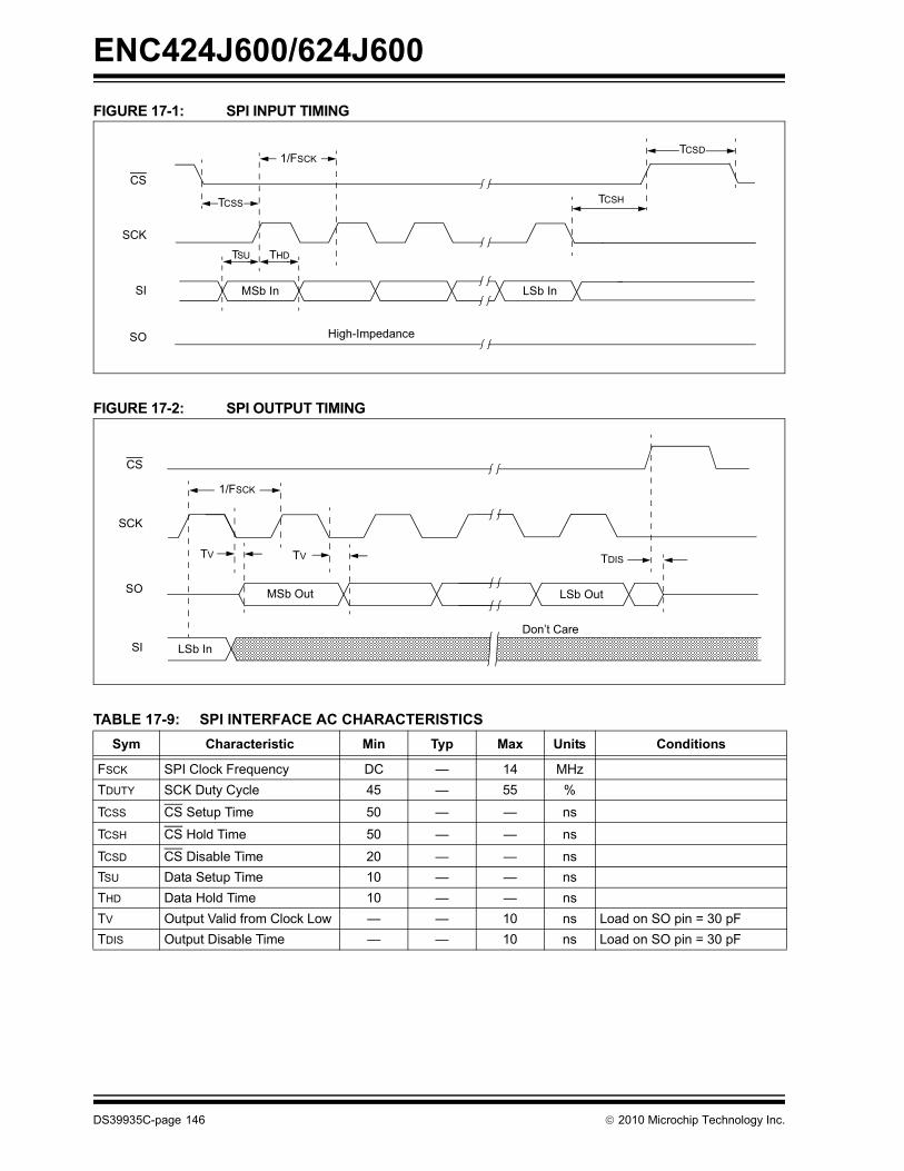
ENC424J600/624J600
FIGURE 17-1: SPI INPUT TIMING
FIGURE 17-2: SPI OUTPUT TIMING
TABLE 17-9: SPI INTERFACE AC CHARACTERISTICS
Sym Characteristic Min Typ Max Units Conditions
FSCK SPI Clock Frequency DC — 14 MHz
TDUTY SCK Duty Cycle 45 — 55 %
TCSS CS Setup Time 50 — — ns
TCSH CS Hold Time 50 — — ns
TCSD CS Disable Time 20 — — ns
TSU Data Setup Time 10 — — ns
THD Data Hold Time 10 — — ns
TV Output Valid from Clock Low — — 10 ns Load on SO pin = 30 pF
TDIS Output Disable Time — — 10 ns Load on SO pin = 30 pF
CS
SCK
SI
SO
TCSS
THDTSU
TCSD
LSb InMSb In
High-Impedance
TCSH
1/FSCK
CS
SCK
SO MSb Out LSb Out
TDIS
Don’t Care
SI
TV TV
LSb In
1/FSCK
DS39935C-page 146 2010 Microchip Technology Inc.

ENC424J600/624J600
TABLE 17-10: PSP INTERFACE TIMING SPECIFICATIONS
Sym Characteristic Min Typ Max Units Comments
TPSP1 CS, Address, R/W Setup Time 1 — — ns
TPSP2 RD, EN, BxSEL to Data Valid — — 75 ns
TPSP3 Data Output Hold Time 0 — 3 ns
TPSP4 RD, EN, BxSEL Deassertion Time
4.5 — — ns
TPSP5 CS, R/W Setup Time 3.5 — — ns
TPSP6 Address Setup Time 3.5 — — ns
TPSP7 Data Setup Time 3.5 — — ns
TPSP8 WR, WRL, WRH, EN, BxSEL Assertion Time
6.5 — — ns
TPSP9 Address Hold Time 1 — — ns
TPSP10 Data Input Hold Time 1 — — ns
TPSP11 WR, WRL, WRH, EN, BxSEL Deassertion Time
4.5 — — ns SFR access
40 — — ns SRAM access
TPSP12 CS, Address Setup Time 6.5 — — ns
TPSP13 AL Assertion Time 6.5 — — ns
TPSP14 Address Hold Time 1 — — ns
TPSP15 AL Deassertion Time 4 — — ns
2010 Microchip Technology Inc. DS39935C-page 147

ENC424J600/624J600
NOTES:
DS39935C-page 148 2010 Microchip Technology Inc.

ENC424J600/624J600
18.0 PACKAGING INFORMATION
18.1 Package Marking Information
Legend: XX...X Customer-specific informationY Year code (last digit of calendar year)YY Year code (last 2 digits of calendar year)WW Week code (week of January 1 is week ‘01’)NNN Alphanumeric traceability code Pb-free JEDEC designator for Matte Tin (Sn)* This package is Pb-free. The Pb-free JEDEC designator ( )
can be found on the outer packaging for this package.
Note: In the event the full Microchip part number cannot be marked on one line, it willbe carried over to the next line, thus limiting the number of availablecharacters for customer-specific information.
3e
XXXXXXXXXX
44-Lead QFN
XXXXXXXXXXXXXXXXXXXX
YYWWNNN
ENC424J600
Example
-I/ML1010017
44-Lead TQFP
XXXXXXXXXXXXXXXXXXXXXXXXXXXXXX
YYWWNNN
Example
ENC424J600-I/PT
1010017
64-Lead TQFP (10x10x1mm)
XXXXXXXXXXXXXXXXXXXXXXXXXXXXXX
YYWWNNN
Example
ENC624J600-I/PT
1010017
3e
3e
3e
2010 Microchip Technology Inc. DS39935C-page 149

ENC424J600/624J600
18.2 Package Details
The following sections give the technical details of thepackages.
!
" !"# $% &" ' ()"&'"!&) & #*&& & # + !!*!"& #, ' !#& -./
012 0!' ! & $& " !**&"&& !-32 % ' !("!"*&"&& (%%'&"! !
" 3& '!&" &+ #*!( ! ! & + %&& #&&&244***''4+
5&! 66--' !6'&! 7 78 9
7"') %! 7 & /018 : & ; &#%% /1&&+ !! , -38 <#& - ;01-$! ##<#& - , / ;8 6 & ;01-$! ##6 & , / ;1&&<#& ) / , ,;1&&6 & 6 , /1&&&-$! ## = > >
D EXPOSEDPAD
D2
e
b
KL
E2
21
NNOTE 1
21
E
N
BOTTOM VIEWTOP VIEW
A3 A1
A
* 1,0
DS39935C-page 150 2010 Microchip Technology Inc.

ENC424J600/624J600
!
" 3& '!&" &+ #*!( ! ! & + %&& #&&&244***''4+
2010 Microchip Technology Inc. DS39935C-page 151

ENC424J600/624J600
#$ %&#'('(')*(( #!
" !"# $% &" ' ()"&'"!&) & #*&& & # 1'% !& ! &?!@ ' , ' !!#-#&"# '#%!&"!!#%!&"!!!& $ #/'' !# ' !#& -./
012 0!' ! & $& " !**&"&& !-32 % ' !("!"*&"&& (%%'&"! !
" 3& '!&" &+ #*!( ! ! & + %&& #&&&244***''4+
5&! 66--' !6'&! 7 78 9
7"') %6 #! 7 6 #& ;018 : & > > # #+ + !! / /&#%% / > /3&6 & 6 / /3&& 6 -33& A ,/A A8 <#& - 018 6 & 01# #+ <#& - 01# #+ 6 & 016 #+ !! > 6 #<#& ) , , /#%& A A ,A#%& 0&&' A A ,A
A
E
E1
DD1
e
b
NOTE 1NOTE 2
N
1 2 3
c
A1L
A2L1
α
φ
β
* 10
DS39935C-page 152 2010 Microchip Technology Inc.

ENC424J600/624J600
#$ %&#'('(')*(( #!
" 3& '!&" &+ #*!( ! ! & + %&& #&&&244***''4+
2010 Microchip Technology Inc. DS39935C-page 153
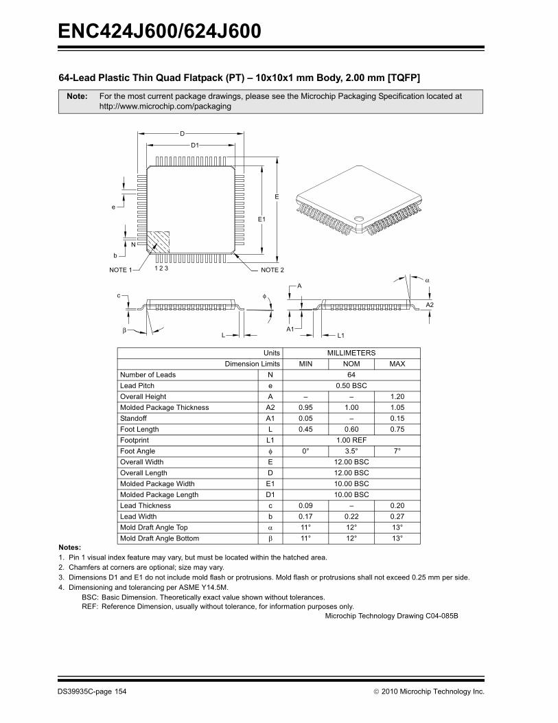
ENC424J600/624J600
+ #$ %&#'('(')*(( #!
" !"# $% &" ' ()"&'"!&) & #*&& & # 1'% !& ! &?!@ ' , ' !!#-#&"# '#%!&"!!#%!&"!!!& $ #/'' !# ' !#& -./
012 0!' ! & $& " !**&"&& !-32 % ' !("!"*&"&& (%%'&"! !
" 3& '!&" &+ #*!( ! ! & + %&& #&&&244***''4+
5&! 66--' !6'&! 7 78 9
7"') %6 #! 7 6 #& /018 : & > > # #+ + !! / /&#%% / > /3&6 & 6 / /3&& 6 -33& A ,/A A8 <#& - 018 6 & 01# #+ <#& - 01# #+ 6 & 016 #+ !! > 6 #<#& ) #%& A A ,A#%& 0&&' A A ,A
D
D1
E
E1
e
b
N
NOTE 1 1 2 3 NOTE 2
c
LA1
L1
A2
Aφ
β
α
* 1;/0
DS39935C-page 154 2010 Microchip Technology Inc.

ENC424J600/624J600
+ #$ %&#'('(')*(( #!
" 3& '!&" &+ #*!( ! ! & + %&& #&&&244***''4+
2010 Microchip Technology Inc. DS39935C-page 155

ENC424J600/624J600
NOTES:
DS39935C-page 156 2010 Microchip Technology Inc.

ENC424J600/624J600
APPENDIX A: REVISION HISTORY
Revision A (March 2009)
Original data sheet for ENC424J600/624J600 devices.
Revision B (July 2009)
Removed preliminary from the data sheet. Section 1.0“Device Overview” and Section 7.0 “Reset” hadminor edits.
Revision C (January 2010)
Section 5.3.3 “MODE 3” and Section 5.3.4 “MODE4” had minor edits.
2010 Microchip Technology Inc. DS39935C-page 157

ENC424J600/624J600
NOTES:
DS39935C-page 158 2010 Microchip Technology Inc.

ENC424J600/624J600
INDEX
AAC Characteristics
CLKOUT Pin ............................................................. 145CLKOUT Pin Timing Specifications .......................... 145ENC424J600/624J600 (Industrial)............................ 145Oscillator Timing ....................................................... 145PSP Interface Timing Specifications......................... 147SPI Interface ............................................................. 146
Advanced Encryption Standard (AES)Context Switching ..................................................... 130Key Support .............................................................. 129
BBlock Diagrams
Alternate TX Choke Topology..................................... 12Bi-Color LED Connection............................................ 12CBC Encryption/Decryption ...................................... 131CFB Encryption/Decryption....................................... 132Crystal Oscillator Operation .......................................... 9CTR Encryption/Decryption ...................................... 134ECB Encryption/Decryption ...................................... 130ENC424J600/624J600.................................................. 6Ethernet Packet Format .............................................. 71Example TX Buffer Wrapping ..................................... 83External Clock Source .................................................. 9I/O Level Shifting on SPI Interface
Using 3-State Buffers.......................................... 15I/O Level Shifting on SPI Interface
Using AND Gates ............................................... 15Interrupt Logic ........................................................... 117OFB Encryption/Decryption ...................................... 133On-Chip Reset Circuit ................................................. 73PSP External Connections Mode 1............................. 54PSP External Connections Mode 10........................... 69PSP External Connections Mode 2............................. 55PSP External Connections Mode 3............................. 57PSP External Connections Mode 4............................. 59PSP External Connections Mode 5............................. 62PSP External Connections Mode 6............................. 65PSP External Connections Mode 9............................. 67RBIAS Resistor ........................................................... 10Receive Filter Decision Tree....................................... 98Single Color LED Connection ..................................... 12Typical Ethernet Magnetics Connections.................... 11Using INT/SPISEL Pin to Select I/O Interface ............ 13VCAP Connections....................................................... 10
Buffer Pointers (SRAM Access).......................................... 34
CCLKOUT Pin ......................................................................... 9CRC
Frame Field................................................................. 72Cryptographic Security Engines
Advanced Encryption Standard (AES)...................... 129Cipher Block Chaining Mode (CBC) ................. 131Cipher Feedback Mode (CFB) .......................... 132Counter Mode (CTR) ........................................ 134Electronic Code Book Mode (ECB) .................. 130Output Feedback Mode (OFB) ......................... 133
MD5/SHA-1 Hashing................................................. 126Context Switching ............................................. 128
Modular Exponentiation ............................................ 125
Customer Change Notification Service............................. 162Customer Notification Service .......................................... 162Customer Support............................................................. 162
DDC Characteristics
ENC424J600/624J600 (Industrial) ........................... 143Internal Voltage Regulator........................................ 144Requirements for External Magnets ......................... 144Thermal Operating Conditions.................................. 142Thermal Packaging................................................... 142
Destination Address............................................................ 71Device Features (table) ........................................................ 5Device Initialization ....................................................... 75–76Digital I/O Levels................................................................. 15Direct Memory Access (DMA) Controller.......................... 123DMA Controller
Checksum Calculations ............................................ 124Copying Memory ...................................................... 123Performance ............................................................. 124
EE Registers ......................................................................... 19Electrical Characteristics .................................................. 141
Absolute Maximum Ratings...................................... 141ENC424J600/624J600 Register File Summary............ 26–27Energy Detect Power-Down ............................................. 137Equations
Increment Logic for EGPRDPT and EGPWRPT ........ 35Increment Logic for ERXRDPT and ERXWRPT......... 36Increment Logic for EUDARDPT
and EUDAWRPT................................................ 36Errata .................................................................................... 4Ethernet
Frame Format............................................................. 71Ethernet Frame Format ...................................................... 71Ethernet Overview .............................................................. 71Examples
Deriving a Hash Table Location ............................... 100External Connections
CS/CS Pin .................................................................. 15Digital I/O Levels ........................................................ 15EMI and Layout Considerations ................................. 12LEDA and LEDB......................................................... 12Oscillator....................................................................... 9PSP Host Interface ..................................................... 14RBIAS Pin................................................................... 10SPI Host Interface ...................................................... 14VCAP Pin ..................................................................... 10VDD/VSS Pins.............................................................. 10
External Power-Down....................................................... 138
FFast Link Pulses (FLPs).................................................... 109Flow Control
Automatic Control ..................................................... 106Full-Duplex Operation............................................... 105Half-Duplex Operation .............................................. 105Manual Control ......................................................... 106Pause Control Frames.............................................. 105Receive Watermark Register.................................... 106
Frame Padding (Field) ........................................................ 72
2010 Microchip Technology Inc. DS39935C-page 159

ENC424J600/624J600
GGeneral Power-Down Sequence....................................... 137
HHost Interface Pins........................................................ 13–15
II/O Level Shifting................................................................. 15Initialization
After Link Establishment ............................................. 76CLKOUT Frequency ................................................... 75MAC ............................................................................ 75PHY............................................................................. 76Receive Buffer ............................................................ 75Receive Filters ............................................................ 75Reset........................................................................... 75Transmit Buffer ........................................................... 75
INT Pin ................................................................................ 13Internet Address................................................................ 162Interrupts
Sources............................................................. 121–122Wake-on-LAN/Remote Wake-up .............................. 122
INTIEGlobal Interrupt Enable Bit ........................................ 117
MMAC Registers .................................................................... 19Magnetics and External Components ................................. 11MD5 Hashing .................................................................... 126Memory Map
Cryptographic Data Memory ....................................... 32PSP............................................................................. 18SPI .............................................................................. 17SRAM Indirect Access Pointers .................................. 34
Microchip Internet Web Site .............................................. 162Modular Exponentiation Engine ........................................ 125
NN-Byte Instructions
Banked SFR................................................................ 45SRAM Buffer ............................................................... 49Unbanked SFR ........................................................... 47
OOscillator ............................................................................... 9
PPackaging
Details ....................................................................... 150Marking ..................................................................... 149
Parallel Slave Port Interface (PSP)External Connections.................................................. 14Mode 1 ........................................................................ 53Mode 10 ...................................................................... 69Mode 2 ........................................................................ 55Mode 3 ........................................................................ 57Mode 4 ........................................................................ 59Mode 5 ........................................................................ 61Mode 6 ........................................................................ 64Mode 9 ........................................................................ 67Performance Considerations ...................................... 53Physical Implementation ............................................. 51Using The Interface..................................................... 52
PHY Register File Summary ............................................... 31PHY Registers..................................................................... 28PHY Subystem Reset ......................................................... 74
Pin FunctionsA14:A0.......................................................................... 7AD15:AD0..................................................................... 7AL ................................................................................. 7B0SEL/B1SEL .............................................................. 7CLKOUT ....................................................................... 7CS/CS........................................................................... 7EN................................................................................. 7INT................................................................................ 7LEDA/LEDB.................................................................. 7OSC1/OSC2 ................................................................. 8PSPCFG4:PSPCFG0 ................................................... 8RBIAS........................................................................... 8RD ................................................................................ 8RW................................................................................ 8SCK .............................................................................. 8SI .................................................................................. 8SO ................................................................................ 8SPISEL ......................................................................... 8TPIN+/TPIN- ................................................................. 8TPOUT+/TPOUT- ......................................................... 8VCAP ............................................................................. 8VDD/VSS........................................................................ 8VDDOSC/VSSOSC ........................................................... 8VDDPLL/VSSPLL.............................................................. 8VDDRX/VSSRX................................................................ 8VDDTX/VSSTX................................................................. 8WR................................................................................ 8WRH/WRL .................................................................... 8
Pinout Descriptions........................................................... 7–8Power-on Reset .................................................................. 73Power-Saving Features .................................................... 137PSP Mode Selection (table)................................................ 14
RReader Response............................................................. 163Receive Filters .................................................................... 72
Broadcast Collection................................................. 100CRC Error Collection/Rejection .................................. 99Hash Table Collection............................................... 100Magic Packet Collection ........................................... 101Multicast Collection................................................... 100Not-Me Unicast Collection .......................................... 99Pattern Match Collection........................................... 102Pattern Match Collection (example).......................... 103Promiscuous Mode................................................... 102Runt Error Collection/Rejection .................................. 99Unicast Collection ....................................................... 99
Receive Only Reset ............................................................ 74Receiving Packets ........................................................ 86–87
Configuring Reception ................................................ 87ERXHEAD/ERXTAIL Buffer Wrap (example) ............. 86Incoming Packet Storage............................................ 87Receive Status Vector ................................................ 89Receive Status Vector (RSV) ..................................... 87Received Packet in Buffer Memory (example) ........... 88Status Vectors ............................................................ 89
Register MapsCLR (8-Bit PSP).......................................................... 24SET (8-Bit PSP).......................................................... 23SET/CLR (16-Bit PSP)................................................ 25
DS39935C-page 160 2010 Microchip Technology Inc.

ENC424J600/624J600
RegistersECON1 (Ethernet Control 1) ....................................... 90ECON2 (Ethernet Control 2) ....................................... 77EIDLED (Ethernet ID Status/LED Control).................. 79EIE (Ethernet Interrupt Enable)................................. 120EIR (Ethernet Interrupt Flag)..................................... 118ERXFCON (Ethernet RX Filter Control)...................... 96ERXWM (Receive Watermark) ................................. 106ESTAT (Ethernet Status) ............................................ 93ETXSTAT (Ethernet Transmit Status)......................... 92MABBIPG (MAC Back-to-Back
Inter-Packet Gap) ............................................... 81MACLCON (MAC Collision Control) ........................... 82MACON1 (MAC Control 1)........................................ 107MACON2 (MAC Control 2).......................................... 80MAIPG (MAC Inter-Packet Gap)................................. 82MICMD (MII Management Command)........................ 30MIREGADR (MII Management Address) .................... 29MISTAT (MII Management Status) ............................. 30PHANA (PHY Auto-Negotiation
Advertisement).................................................. 113PHANE (PHY Auto-Negotiation Expansion) ............. 115PHANLPA (PHY Auto-Negotiation Link
Partner Ability) .................................................. 114PHCON1 (PHY Control 1)......................................... 110PHCON2 (PHY Control 2)......................................... 139PHSTAT1 (PHY Status 1)......................................... 111PHSTAT2 (PHY Status 2)......................................... 112PHSTAT3 (PHY Status 3)......................................... 112
ResetPHY Subsystem.......................................................... 74Power-on..................................................................... 73Receive Only............................................................... 74System ........................................................................ 73Transmit Only.............................................................. 74
Revision History ................................................................ 157
SSerial Peripheral Interface (SPI)
External Connections.................................................. 14Instruction Set ............................................................. 39Physical Implementation ............................................. 39
SFR. See Special Function Registers................................. 19SHA-1 Hashing ................................................................. 126Single Byte Instructions ...................................................... 41Source Address .................................................................. 72Special Function Registers ................................................. 19
Address Map16-Bit PSP .......................................................... 228-Bit PSP ............................................................ 21SPI ...................................................................... 20
PHY Registers ............................................................ 28Speed/Duplex Auto-Negotiation........................................ 109
Manual Configuration................................................ 109SPI Instruction Set
N-Byte InstructionsBanked SFR ....................................................... 45SRAM Buffer ....................................................... 49Unbanked SFR ................................................... 47
Single Byte Instructions .............................................. 41Summary Table........................................................... 40Three-Byte Instructions............................................... 43Two-Byte Instructions ................................................. 42
SRAM Buffer....................................................................... 32Buffer Pointers............................................................ 34Circular Wrapping
ERXDATA Pointer .............................................. 36EUDADATA Pointer...................................... 36–37
Circular Wrapping with EGPDATA Pointer ................. 35Direct Access.............................................................. 33General Purpose Buffer.............................................. 33Indirect Access ........................................................... 34Receive Buffer ............................................................ 33Transmit Buffer ........................................................... 33
Start-Of-Frame Delimiter .................................................... 71Start-of-Stream/Preamble Field .......................................... 71System Reset ..................................................................... 73
TThree-Byte Instructions....................................................... 43Timing Diagrams
N-Byte SPI Instruction (Banked SFR Operations) .................................. 45
N-Byte SPI Opcode (Unbanked SFR Operations) .............................. 47
N-Byte SPI Opcode Instruction (SRAM Buffer Operations).................................. 49
PSP Mode 1 Read...................................................... 54PSP Mode 1 Write ...................................................... 54PSP Mode 10 Read.................................................... 70PSP Mode 10 Write .................................................... 70PSP Mode 2 Read...................................................... 56PSP Mode 2 Write ...................................................... 56PSP Mode 3 Read...................................................... 58PSP Mode 3 Write ...................................................... 58PSP Mode 4 Read...................................................... 60PSP Mode 4 Write ...................................................... 60PSP Mode 5 Read...................................................... 63PSP Mode 5 Write ...................................................... 63PSP Mode 6 Read...................................................... 66PSP Mode 6 Write ...................................................... 66PSP Mode 9 Read...................................................... 68PSP Mode 9 Write ...................................................... 68Single Byte Instruction................................................ 41SPI Input................................................................... 146SPI Output ................................................................ 146Three-Byte Read Instruction....................................... 43Three-Byte Write Instruction....................................... 43Two-Byte Instruction (RBSEL Opcode) ...................... 42
Transmit Only Reset ........................................................... 74Transmitting Packets .................................................... 83–86
Selecting ETXLEN Values (example)......................... 84Special Cases............................................................. 85Transmission Status ................................................... 85
Two-Byte Instructions ......................................................... 42Type/Length Field ............................................................... 72
WWake-on-LAN/Remote Wake-up ...................................... 122WWW Address ................................................................. 162WWW, On-Line Support ....................................................... 4
2010 Microchip Technology Inc. DS39935C-page 161

ENC424J600/624J600
NOTES:
DS39935C-page 162 2010 Microchip Technology Inc.

ENC424J600/624J600
THE MICROCHIP WEB SITE
Microchip provides online support via our WWW site atwww.microchip.com. This web site is used as a meansto make files and information easily available tocustomers. Accessible by using your favorite Internetbrowser, the web site contains the followinginformation:
• Product Support – Data sheets and errata, application notes and sample programs, design resources, user’s guides and hardware support documents, latest software releases and archived software
• General Technical Support – Frequently Asked Questions (FAQ), technical support requests, online discussion groups, Microchip consultant program member listing
• Business of Microchip – Product selector and ordering guides, latest Microchip press releases, listing of seminars and events, listings of Microchip sales offices, distributors and factory representatives
CUSTOMER CHANGE NOTIFICATION SERVICE
Microchip’s customer notification service helps keepcustomers current on Microchip products. Subscriberswill receive e-mail notification whenever there arechanges, updates, revisions or errata related to aspecified product family or development tool of interest.
To register, access the Microchip web site atwww.microchip.com, click on Customer ChangeNotification and follow the registration instructions.
CUSTOMER SUPPORT
Users of Microchip products can receive assistancethrough several channels:
• Distributor or Representative
• Local Sales Office
• Field Application Engineer (FAE)
• Technical Support
• Development Systems Information Line
Customers should contact their distributor,representative or field application engineer (FAE) forsupport. Local sales offices are also available to helpcustomers. A listing of sales offices and locations isincluded in the back of this document.
Technical support is available through the web siteat: http://support.microchip.com
2010 Microchip Technology Inc. DS39935C-page 163

ENC424J600/624J600
READER RESPONSE
It is our intention to provide you with the best documentation possible to ensure successful use of your Microchip prod-uct. If you wish to provide your comments on organization, clarity, subject matter, and ways in which our documentationcan better serve you, please FAX your comments to the Technical Publications Manager at (480) 792-4150.
Please list the following information, and use this outline to provide us with your comments about this document.
To: Technical Publications Manager
RE: Reader Response
Total Pages Sent ________
From: Name
Company
Address
City / State / ZIP / Country
Telephone: (_______) _________ - _________
Application (optional):
Would you like a reply? Y N
Device: Literature Number:
Questions:
FAX: (______) _________ - _________
DS39935CENC424J600/624J600
1. What are the best features of this document?
2. How does this document meet your hardware and software development needs?
3. Do you find the organization of this document easy to follow? If not, why?
4. What additions to the document do you think would enhance the structure and subject?
5. What deletions from the document could be made without affecting the overall usefulness?
6. Is there any incorrect or misleading information (what and where)?
7. How would you improve this document?
DS39935C-page 164 2010 Microchip Technology Inc.

2010 Microchip Technology Inc. DS39935C-page 165
ENC424J600/624J600
PRODUCT IDENTIFICATION SYSTEM
To order or obtain information, e.g., on pricing or delivery, refer to the factory or the listed sales office.
PART NO. X /XX XXX
PatternPackageTemperatureRange
Device
Device ENC424J600, ENC624J600, ENC424J600T(1), ENC624J600T(1); VDD range 3.0V to 3.6V
Temperature Range I = -40C to +85C (Industrial)
Package ML = QFN (Quad Flat No Lead)PT = TQFP (Thin Quad Flatpack)
Pattern Three-Digit Code or Special Requirements (blank otherwise)
ES = Engineering Sample
Examples:
a) ENC424J600-I/ML = Industrial temp., QFN package.
b) ENC424J600-I/PT = Industrial temp., 44 leads TQFP package.
c) ENC624J600T-I/PT = Industrial temp., 64 leads TQFP package, tape and reel.
Note 1: T = in tape and reel.

DS39935C-page 166 2010 Microchip Technology Inc.
AMERICASCorporate Office2355 West Chandler Blvd.Chandler, AZ 85224-6199Tel: 480-792-7200 Fax: 480-792-7277Technical Support: http://support.microchip.comWeb Address: www.microchip.com
AtlantaDuluth, GA Tel: 678-957-9614 Fax: 678-957-1455
BostonWestborough, MA Tel: 774-760-0087 Fax: 774-760-0088
ChicagoItasca, IL Tel: 630-285-0071 Fax: 630-285-0075
ClevelandIndependence, OH Tel: 216-447-0464 Fax: 216-447-0643
DallasAddison, TX Tel: 972-818-7423 Fax: 972-818-2924
DetroitFarmington Hills, MI Tel: 248-538-2250Fax: 248-538-2260
KokomoKokomo, IN Tel: 765-864-8360Fax: 765-864-8387
Los AngelesMission Viejo, CA Tel: 949-462-9523 Fax: 949-462-9608
Santa ClaraSanta Clara, CA Tel: 408-961-6444Fax: 408-961-6445
TorontoMississauga, Ontario, CanadaTel: 905-673-0699 Fax: 905-673-6509
ASIA/PACIFICAsia Pacific OfficeSuites 3707-14, 37th FloorTower 6, The GatewayHarbour City, KowloonHong KongTel: 852-2401-1200Fax: 852-2401-3431
Australia - SydneyTel: 61-2-9868-6733Fax: 61-2-9868-6755
China - BeijingTel: 86-10-8528-2100 Fax: 86-10-8528-2104
China - ChengduTel: 86-28-8665-5511Fax: 86-28-8665-7889
China - ChongqingTel: 86-23-8980-9588Fax: 86-23-8980-9500
China - Hong Kong SARTel: 852-2401-1200 Fax: 852-2401-3431
China - NanjingTel: 86-25-8473-2460Fax: 86-25-8473-2470
China - QingdaoTel: 86-532-8502-7355Fax: 86-532-8502-7205
China - ShanghaiTel: 86-21-5407-5533 Fax: 86-21-5407-5066
China - ShenyangTel: 86-24-2334-2829Fax: 86-24-2334-2393
China - ShenzhenTel: 86-755-8203-2660 Fax: 86-755-8203-1760
China - WuhanTel: 86-27-5980-5300Fax: 86-27-5980-5118
China - XianTel: 86-29-8833-7252Fax: 86-29-8833-7256
China - XiamenTel: 86-592-2388138 Fax: 86-592-2388130
China - ZhuhaiTel: 86-756-3210040 Fax: 86-756-3210049
ASIA/PACIFICIndia - BangaloreTel: 91-80-3090-4444 Fax: 91-80-3090-4123
India - New DelhiTel: 91-11-4160-8631Fax: 91-11-4160-8632
India - PuneTel: 91-20-2566-1512Fax: 91-20-2566-1513
Japan - YokohamaTel: 81-45-471- 6166 Fax: 81-45-471-6122
Korea - DaeguTel: 82-53-744-4301Fax: 82-53-744-4302
Korea - SeoulTel: 82-2-554-7200Fax: 82-2-558-5932 or 82-2-558-5934
Malaysia - Kuala LumpurTel: 60-3-6201-9857Fax: 60-3-6201-9859
Malaysia - PenangTel: 60-4-227-8870Fax: 60-4-227-4068
Philippines - ManilaTel: 63-2-634-9065Fax: 63-2-634-9069
SingaporeTel: 65-6334-8870Fax: 65-6334-8850
Taiwan - Hsin ChuTel: 886-3-6578-300Fax: 886-3-6578-370
Taiwan - KaohsiungTel: 886-7-536-4818Fax: 886-7-536-4803
Taiwan - TaipeiTel: 886-2-2500-6610 Fax: 886-2-2508-0102
Thailand - BangkokTel: 66-2-694-1351Fax: 66-2-694-1350
EUROPEAustria - WelsTel: 43-7242-2244-39Fax: 43-7242-2244-393Denmark - CopenhagenTel: 45-4450-2828 Fax: 45-4485-2829
France - ParisTel: 33-1-69-53-63-20 Fax: 33-1-69-30-90-79
Germany - MunichTel: 49-89-627-144-0 Fax: 49-89-627-144-44
Italy - Milan Tel: 39-0331-742611 Fax: 39-0331-466781
Netherlands - DrunenTel: 31-416-690399 Fax: 31-416-690340
Spain - MadridTel: 34-91-708-08-90Fax: 34-91-708-08-91
UK - WokinghamTel: 44-118-921-5869Fax: 44-118-921-5820
WORLDWIDE SALES AND SERVICE
01/05/10