EMERGING SUBSTRATE TECHNOLOGIES FOR … printed wiring board production in 2008 ... Electronic...
7
EMERGING SUBSTRATE TECHNOLOGIES FOR PACKAGING Henry H. Utsunomiya Interconnection Technologies, Inc. Suwa City, Nagano Prefecture, Japan [email protected] ABSTRACT This presentation will outline the market dynamics driving the development of advanced substrates in today’s industry landscape. Technological advancements have shifted from Personal Computers to Mobile Applications like Cellular phones, MPEG players, etc. An overview of the technology revolution of substrates and their corresponding packages will be discussed in terms of technology supply chain matching: assembly technology, substrate technology and system technology. Advanced substrate technology roadmaps of leading Japanese suppliers will be reviewed. The evolution of buildup substrates, which have standardized under the direction of CPU & FPGA manufacturers will be explained. The two technological directions of substrates for advanced electronic packages will be mapped out: miniaturization and functional integration, and explained in terms of “More Moore” and “More than Moore”, respectively. Fine pitch wiring on substrates can be combined with embedded active and passive devices and has been proven as a technology. Examples/ illustrations of advanced substrate applications in servers, hand -helds, and high end servers and communication equipments will be reviewed: PoP, Embedded Active Devices, Si interposers and Wafer Level Packages, etc. Key words: Packaging substrate, Embedded Active Devices, Si Interposer, Wafer Level Package, PoP INTRODUCTION Worldwide printed wiring board production in 2008 was estimated 51,530 million US$ and Japan was produced 11,561 million US$ (22.4 %) by WECC (World Electronic Circuits Council) Global PCB production Report. And worldwide packaging substrate production in 2008 was estimated 8,925 million US$. In 2008, Japan produced 4,414 million US$ packaging substrate and total share was 49.5 %. Taiwan is second large production of packaging substrate with 2,316 million US$ and Korea followed Taiwan with 1,410 million US$ [1] . Japanese domestic packaging substrate production amount in 2008, buildup structure substrate shares 55.4 % and rigid structure substrate shares 20.1 %, while tape structure substrate including TAB (Tape Automated Bonding) and COF (Chip on Film/Flexible) shares 19.3 %. Package substrate production in 2009 is expected to be divided as follows; rigid substrates are estimated to be 35.6 Billion ¥, 11.7 % share, buildup substrates are estimated to be 190.0 Billion ¥, 62.5 %, and the tape substrate share is estimated to be 61.2 Billion ¥ or 20.1 % share [2] . In addition, Japanese packaging substrate manufacturers expect a CAGR of 11.9 % (2009 to 2013) for next 5 years. Figure 1 and figure 2 are illustrated Japanese packaging substrate production amount progress and Japanese printed wiring boards production amount progress respectively. Figure 1. Japanese Packaging Substrate Production Amount Progress (Unit: 100 Million ¥) [2] Figure 2. Japanese PWB Production Amount Progress (Unit: 100 Million ¥) [2] As originally published in the Pan Pacific Symposium Proceedings.
Transcript of EMERGING SUBSTRATE TECHNOLOGIES FOR … printed wiring board production in 2008 ... Electronic...

EMERGING SUBSTRATE TECHNOLOGIES FOR PACKAGING
Henry H. Utsunomiya Interconnection Technologies, Inc.
Suwa City, Nagano Prefecture, Japan [email protected]
ABSTRACT This presentation will outline the market dynamics driving the development of advanced substrates in today’s industry landscape. Technological advancements have shifted from Personal Computers to Mobile Applications like Cellular phones, MPEG players, etc. An overview of the technology revolution of substrates and their corresponding packages will be discussed in terms of technology supply chain matching: assembly technology, substrate technology and system technology. Advanced substrate technology roadmaps of leading Japanese suppliers will be reviewed. The evolution of buildup substrates, which have standardized under the direction of CPU & FPGA manufacturers will be explained. The two technological directions of substrates for advanced electronic packages will be mapped out: miniaturization and functional integration, and explained in terms of “More Moore” and “More than Moore”, respectively. Fine pitch wiring on substrates can be combined with embedded active and passive devices and has been proven as a technology. Examples/ illustrations of advanced substrate applications in servers, hand -helds, and high end servers and communication equipments will be reviewed: PoP, Embedded Active Devices, Si interposers and Wafer Level Packages, etc. Key words: Packaging substrate, Embedded Active Devices, Si Interposer, Wafer Level Package, PoP INTRODUCTION Worldwide printed wiring board production in 2008 was estimated 51,530 million US$ and Japan was produced 11,561 million US$ (22.4 %) by WECC (World Electronic Circuits Council) Global PCB production Report. And worldwide packaging substrate production in 2008 was estimated 8,925 million US$. In 2008, Japan produced 4,414 million US$ packaging substrate and total share was 49.5 %. Taiwan is second large production of packaging substrate with 2,316 million US$ and Korea followed Taiwan with 1,410 million US$ [1]. Japanese domestic packaging substrate production
amount in 2008, buildup structure substrate shares 55.4 % and rigid structure substrate shares 20.1 %, while tape structure substrate including TAB (Tape Automated Bonding) and COF (Chip on Film/Flexible) shares 19.3 %. Package substrate production in 2009 is expected to be divided as follows; rigid substrates are estimated to be 35.6 Billion ¥, 11.7 % share, buildup substrates are estimated to be 190.0 Billion ¥, 62.5 %, and the tape substrate share is estimated to be 61.2 Billion ¥ or 20.1 % share [2]. In addition, Japanese packaging substrate manufacturers expect a CAGR of 11.9 % (2009 to 2013) for next 5 years. Figure 1 and figure 2 are illustrated Japanese packaging substrate production amount progress and Japanese printed wiring boards production amount progress respectively.
Figure 1. Japanese Packaging Substrate Production Amount Progress (Unit: 100 Million ¥) [2]
Figure 2. Japanese PWB Production Amount Progress (Unit: 100 Million ¥) [2]
As originally published in the Pan Pacific Symposium Proceedings.

Figure 3 and figure 4 are shown printed wiring board products production amount share in 2007 and average growth rate of 2005 – 2007, and PWB production amount share in 2008 and CAGR 2005 - 2008 respectively.
Figure 3. PWB Production Amount Share & CAGR in 2007 (Unit: Million US$) [3]
Figure 4. PWB Production Amount Share & CAGR in 2008 (Unit: Million US$) [3] BACK GROUND OF PACKAGING SUBSTRATE ROADMAP Actual scaling of semiconductor is more accelerated than ITRS roadmap and 32 nm technology nodes was announced by Intel and IBM such as SRAM using 19 billion transistors and 22 nm SRAM development in 2008 and 2009 respectively. To accomplish 32 nm technology nodes, several challenges on reducing power consumption, improving signal speed and external data transmission speed are required for reduced leakage current, reducing coupling for minimized signal propagation delay, and increased data bus width by increased number of I/O terminals. Scaling of semiconductor enable to reduce gate delay, while interconnect delay increasing exponentially due to
resistivity increased by narrower wiring and increased length of global wiring. In addition, I/O terminal pitch should be decreased to less than 125 μm to assure power integrity. Figure 5 is shown performance bottleneck by interconnect delay and figure 6 is shown technology innovation by data bus width.
Figure 5. Performance Bottleneck by Interconnect Delay [4]
Figure 6. Technology Innovation by Data Bus Width [5] For flip chip package, organic substrate is difficult to adopt high bump account and less than 100 μm bump pitch with economical cost due to difficulty on 15 - 10 μm via hole diameter generation with existed laser drilling process. More over difficulty on 5 μm line width and space generation with 50 μm via diameter by current CO2 laser drilling. In addition, in small form factor portable products required 150 μm solder ball pitch for motherboard in 2011. For very fine pitch chip package bonding, alternative technology such as silicon interposer with TSV is one of candidate technology to solve finer wiring and via diameter for high-end applications. And fan-out CSP can ease to solder ball pitch for portable products. In addition, embedded devices into substrates, motherboards and module boards will enable to solve these issues. Table 1 is shown chip to package interconnect technology requirements and Table 2 is shown package to board interconnect technology requirement.
As originally published in the Pan Pacific Symposium Proceedings.

Table 1. Chip to Package Technology Requirements [6]
Table 2. Package to Board Technology Requirements [6]
Generally, motherboard design rule is define one line between via holes and major mounted device package is fine pitch BGA, while packaging substrate design rule is defined two or three lines between via holes. For 0.15 mm pitch solder ball F-BGA requires 40 μm via diameter on 75 μm land diameter with 25 μm line width/space, generally. In case of flip chip bump pitch of 100 μm, 30 μm to 50 μm via diameter on 70 μm land diameter with 6 μm line width/space is needed for 2 lines between via holes and 3 μm line width/space is needed for 3 lines between via holes with same via land diameter. For 30 μm via formation, it is capability limitation of UV-YAG laser and it may require Excimer laser. However, through put of Excimer laser is not enough for huge number of via holes formation. Table 3 is shown general design rules on motherboard and substrate.
Table 3. General Design Rules for Motherboard & Substrate [7]
SUBSTRATE TECHNOLOGY ROADMAP For packaging substrate roadmap, we classified technology difficulties into 6 categories such as “Low Cost”: P-BGA for conventional consumer products with conventional technology, “Hand-held”: FBGA (CSP) for portable products, “Mobile Products”: SiP and PoP for smart phone and mobile PC, “Cost Performance”: Buildup substrate P-BGA for CPU, GPU and game processor, “High Performance High End” Buildup substrate P-BGA and Silicon interposer BGA for high end routers, and “High Performance”: LTCC BGA for routers and servers. Table 4 is shown typical package type of each application. Table 4. Description of Typical Package Type by Application [6]
In mobile products application, the combination of high glass transition temperature FR-4 and epoxy film is dominant today. Minimum line width/space of 20 μm/20μm today will decrease to 15μm/15μm in 2012 and it will expect to less than 10 μm in 2018. However, micro via diameter scaling
As originally published in the Pan Pacific Symposium Proceedings.

is moderate and 80 μm today will expect to down to 50 μm in 2018, due to economical reason such as maintain via formation process cost and save capital investment for new laser drilling system. Table 5 is shown mobile product substrate roadmap. Table 5. Mobile Products Substrate Roadmap [6]
Most of CPU, graphic processing engine and game processor are using flip chip interconnect today and it expect to use flip chip until 2020 for cost performance application. Since flip chip bump pitch will decrease from 150 μm today to 80 μm in 2018 due to die size shrinkage are happen for each technology nodes, minimum line width/space have to reach 5μm/5μm with 30 μm via diameter with UV-YAG laser or excimer laser. One of biggest issue on buildup material is residues are remain on the bottom of via holes after desmear process and it affects interconnect reliability. To accomplish sub ten micron wiring together with finer via diameter, material improvement including lower CTE with less fillers, very smooth surface morphology such as less than 100 nm average flatness for finer circuit, lower dielectric loss and optimized Young’s modulus are necessary within next 5 years. Table 6 is shown cost performance substrate roadmap. Table 6. Cost Performance Substrate Roadmap [6]
With the semiconductor die size becoming larger, matching of thermal expansion coefficient between the die and packaging substrate becomes critical for high-end high performance application. At present, 8 - 10 ppm/°C is required for core material and 16 ppm/°C for buildup layer material with reinforcement material such as SiO2 fillers and/or glass yearns. In 2010, most tightest flip chip bump pitch become 125 - 100 μm, silicon interposer with polyimide redistribution layers will introduce to this application. And dielectric material for redistribution layer and/or functional layer materials will change to meso-porous silicon dioxide materials to adopt smaller CTE, mechanical strength and finer circuit in 2015 for tera bit scale data transmission package. One of potential solution is existed for current ultra low κ material for less than 32 nm technology node semiconductors. Table 7 is shown high-end high performance packaging substrate roadmap. Table 7. High-End High Performance Substrate Roadmap [6]
PACKAGING SUBSTRATE TECHNOLOGY ROADMAP Packaging substrate manufacturers in Japan are expects minimum line width and space of 7.5 μm/7.5 μm volume production will start in 2010 and 5.0 μm/5.0 μm volume production will start in 2014 according to survey results of Jisso Technology Roadmap 2009 edition, as shown in figure 7.
As originally published in the Pan Pacific Symposium Proceedings.
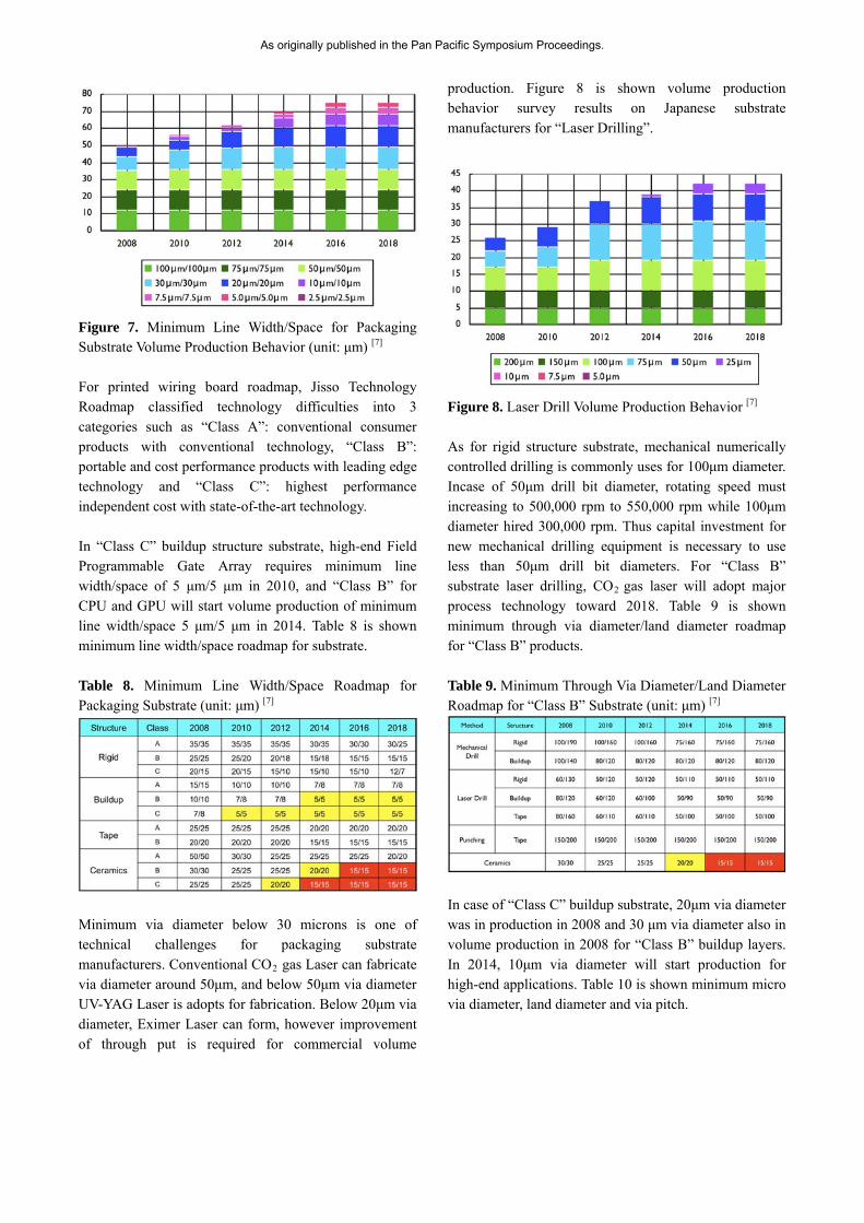
Figure 7. Minimum Line Width/Space for Packaging Substrate Volume Production Behavior (unit: μm) [7] For printed wiring board roadmap, Jisso Technology Roadmap classified technology difficulties into 3 categories such as “Class A”: conventional consumer products with conventional technology, “Class B”: portable and cost performance products with leading edge technology and “Class C”: highest performance independent cost with state-of-the-art technology. In “Class C” buildup structure substrate, high-end Field Programmable Gate Array requires minimum line width/space of 5 μm/5 μm in 2010, and “Class B” for CPU and GPU will start volume production of minimum line width/space 5 μm/5 μm in 2014. Table 8 is shown minimum line width/space roadmap for substrate. Table 8. Minimum Line Width/Space Roadmap for Packaging Substrate (unit: μm) [7]
Minimum via diameter below 30 microns is one of technical challenges for packaging substrate manufacturers. Conventional CO2 gas Laser can fabricate via diameter around 50μm, and below 50μm via diameter UV-YAG Laser is adopts for fabrication. Below 20μm via diameter, Eximer Laser can form, however improvement of through put is required for commercial volume
production. Figure 8 is shown volume production behavior survey results on Japanese substrate manufacturers for “Laser Drilling”.
Figure 8. Laser Drill Volume Production Behavior [7] As for rigid structure substrate, mechanical numerically controlled drilling is commonly uses for 100μm diameter. Incase of 50μm drill bit diameter, rotating speed must increasing to 500,000 rpm to 550,000 rpm while 100μm diameter hired 300,000 rpm. Thus capital investment for new mechanical drilling equipment is necessary to use less than 50μm drill bit diameters. For “Class B” substrate laser drilling, CO2 gas laser will adopt major process technology toward 2018. Table 9 is shown minimum through via diameter/land diameter roadmap for “Class B” products. Table 9. Minimum Through Via Diameter/Land Diameter Roadmap for “Class B” Substrate (unit: μm) [7]
In case of “Class C” buildup substrate, 20μm via diameter was in production in 2008 and 30 μm via diameter also in volume production in 2008 for “Class B” buildup layers. In 2014, 10μm via diameter will start production for high-end applications. Table 10 is shown minimum micro via diameter, land diameter and via pitch.
As originally published in the Pan Pacific Symposium Proceedings.

Table 10. Minimum Land Diameter, Land Diameter and Via Pitch Roadmap for Substrate (unit: μm) [7]
EMBEDDED ACTIVE DEVICES INTO PACKAGING SUBSTRATE Embedded active devices and passive devices into packaging substrate as well as motherboard is one of potential solution to filled the gap between semiconductors and printed wiring board wiring density. And it is already start volume production in several manufacturers in Japan, Korea and Taiwan. Figure 9 is shown categories of embedded passives and actives.
Figure 9. Categories of Embedded Passive Devices and Embedded Active Devices [7] Regarding on embedded passive devices, there is two major technologies has been used in Japan. One is embedded discrete components such as 0603 (0.6 mm by 0.3 mm) resistors and capacitors with Cu plated terminals are mounted on to printed wiring board inner layer with surface mount equipment, then buried by prepreg or buildup layer materials. The other method is using printed wiring process technologies such as photolithography, etching and plating to form resistor and capacitor functions during PWB fabrication process. Embedded active device is hiring almost same technology of embedded discrete components, however placement of bare die has two directions such as face up and face down.
In the near future, formed active device by functional ink with carrier mobilities of 1 - 10 cm2/Vs will be introduced. Thick film printed methods using gravure, flexography, screen, offset lithography, inkjet will be adopted for functional ink on a substrate. Table 11 is shown example of current status of active device embedded. Table 11. Current Status of Embedded Active/Passive Devices [8]
SUMMARY In the next 5 years, the technology of packaging substrate will drive by flip chip interconnection technology with significant higher pin counts and embedded active and passive devices for System in Package. As a result, organic substrate will face technology limitation and silicon interposer or glass substrate will be introduced for high-end applications. In addition, organic substrate using buildup layers will approach minimum line width/space of 5 μm/5 μm with less than 30μm to 5μm via diameter. Table 12 is addressed very advance PWB business structure comparison between last 5 years and next 5 years. Table 12. Advanced PWB Business Structure [3]
As originally published in the Pan Pacific Symposium Proceedings.

The difficulty of advanced PWB business is capital investment that is tremendous huge for finer wiring board production such as 200 million US$ to 500 million US$ for 50,000 m2 out put /monthly production factory from scratch. However, active devices embedded into printed wiring boards have potential solution to increase functional density without ultra finer wiring. Both finer wiring technology and integrated function into board level will be coexisted in next 5 years. To accomplish this scheme, infrastructural enhancement of materials, manufacturing technologies, quality assurance and modeling and simulation to advanced packaging substrate as well as embedded active devices are necessary. REFERENCES [1] WECC Global PCB Production Report [2] Electronic Circuits Industrial Survey Report 2008 Edition, JPCA [3] World Electronic Circuit Council Global PCB Production Report for 2008 [4] Fraunhofer IZM [5] Toshihiko Nishio, Substrate Technology need by next generation high performance package, 28 Jan., 2009 [6] 2009 International Technology Roadmap for Semiconductors [7] 2009 Jisso Technology Roadmap, JEITA [8] H. Utsunomiya, KPCA International Symposium, 20 Nov., 2009
As originally published in the Pan Pacific Symposium Proceedings.