
embedded systems engineering december 2017 · Embedded Electronics Media Group Clair Bright...
37
Transcript of embedded systems engineering december 2017 · Embedded Electronics Media Group Clair Bright...


1 EMBEDDED SYSTEMS ENGINEERING
FROM THE EDITOR
Embedded Systems Engineering is published by Extension
Media LLC, 1786 18th Street, San Francisco, CA 94107.
Copyright © 2018 by Extension Media LLC. All rights
reserved. Printed in the U.S.
EMBEDDED SYSTEMS ENGINEERING 2017www.embeddedsystemsengineering.com
Vice President & Publisher
Clair Bright
Editorial
Editor-in-Chief
Lynnette Reese ❘ [email protected]
Managing Editor
Anne Fisher ❘ [email protected]
Senior Editors
Caroline Hayes ❘ [email protected]
Dave Bursky ❘ [email protected]
Pete Singer ❘ [email protected]
John Blyler ❘ [email protected]
Creative / Production
Production Traffic Coordinator
Marjorie Sharp
Graphic Designers
Nicky Jacobson
Simone Bradley
Senior Web Developers
Slava Dotsenko
Advertising / Reprint Sales
Vice President, Sales
Embedded Electronics Media Group
Clair Bright
(415) 255-0390 ext. 15
Sales Manager
Elizabeth Thoma
(415) 244-5130
Marketing/Circulation
Jenna Johnson
To Subscribe
www.eecatalog.com
Extension Media, LLC Corporate Office
President and Publisher
Vince Ridley
(415) 255-0390 ext. 18
Vice President & Publisher
Clair Bright
Human Resources / Administration
Darla Rovetti
Special Thanks to Our Sponsors
The Push for Machine Learning on Edge Devices, Including Your Smartphone
Machine learning (ML) execution and inferences are being pushed into so-called “edge”
devices, which includes smartphones. Deloitte Global thinks that 300 million smart-
phones sold in 2017 have on-board ML.1 The migration of intelligence to the edge is necessary
to process data close to the source and augment the cloud. Reasons for moving computing to the
edge include low latency, privacy, and connectivity issues. Pushing ML to edge devices is not the
same as training for machine learning; models are trained on high performance compute platforms, and the
resulting model gets pushed to an edge device. Most understand that an ML model can exist and execute on an
intelligent edge device, but an inference is a different but related concept. An inference refers to neural networks
that infer, or make reasonable assumptions, about new data that comes in based on its existing training model.
Intelligence at the edge is the forefront of Artificial Intelligence (AI) and the Internet of Things (IoT), but
challenges are great when it comes to shoe-horning an ML model into an edge device with resource con-
straints. Nevertheless, the smartphone is the most prevalent compute platform. IHS Markit predicts six
billion smartphones in use by 2020. Applications that use ML will make smartphones more autonomous,
increasing privacy and reliability because they will not have to connect to a cloud as often.
The challenge for AI workloads is that they are
very compute-intensive, involving large and
complicated neural network models with com-
plex concurrencies. Smartphones (and other IoT
devices) always tend to be on and often must
produce results in real time. Constrained envi-
ronments require thermally efficient design to
enable sleek, ultralight devices that need a long
battery life for all-day use and come with storage
and memory limitations. Smartphones and IoT
devices share common challenges. This is one
reason why any improvement in ML algorithms
is a big deal right now. Companies are racing
to optimize space and run-time efficiency for
improving ML on resource-constrained devices. Again, the benefit to computing at the edge versus connecting
to a cloud removes latency and connectivity issues and increases privacy as authentication data is not required
to travel. Face recognition as a method for authenticating payments from a smartphone, for example, needs to
be local to the smartphone to decrease security vulnerabilities and increase reliability.
Away from the developer and in the hands of consumers, Google has created a crowd-sourced training
model called Federated Learning that “enables mobile phones to collaboratively learn a shared prediction
model while keeping all the training data on the device, decoupling the ability to do ML from the need to
store the data in the cloud.” It’s kind of like creating an automated patch on your smartphone to update the
smartphone model in the cloud. You download the current model from the cloud and improve the model
by allowing it to learn from data on your phone. Changes made to the model are sent as a “small, focused
update” which is encrypted and sent to the cloud. This might explain why there’s an increase in crazy sug-
gestions (words I have never seen before) for my Android’s text entries these days.
Lynnette Reese is Editor-in-Chief, Embedded Systems Engineering, and has been working in various roles as an elec-
trical engineer for over two decades.
By Lynnette Reese, Editor-in-Chief, Embedded Systems Engineering
Figure 1: Hardware microservices on FPGA, as depicted in a data center use case. Interconnected FPGAs form a separate plane of computation that can be managed and used independently from the CPU. (Source: Microsoft, Hot Chips7)
1. Neal, Phil. “The Deloitte Consumer Review Digital Predictions 2017.” Deloitte., Deloitte, www.deloitte.co.uk/consumerreview.

December 20172
IN THIS ISSUE
CONTENTS
Departments
From the Editor The Push for Machine Learning on Edge
Devices, Including Your Smartphone
By Lynnette Reese, Editor-in-Chief, Embedded Systems
Engineering 1
Features
The Digitization of Cooking
By Dan Viza, NXP Semiconductors 3
FPGA, PLD & SoC Solutions
Minimizing Latency in Mission-Critical Video Processing Applications
By Haydn Nelson, Abaco Systems 6
How to Verify an SoC Meets Your Power Budget
By Guillaume Boillet and Jean-Marie Brunet, Mentor,
a Siemens business 8
Distributed PLD Solution Reduces Server Costs and Increases Flexibility
By Srirama (Shyam) Chandra, Lattice Semiconductor 11
Bridging the Gap Between Modern, Rigorous FPGA
Development Flow and DO-254/ED-80
By Sergio Marchese, OneSpin Solutions 14
Cover Artificial Intelligence: Where FPGAs Surpass GPUs
By Lynnette Reese, Editor-in-Chief, Embedded Systems
Engineering 17
Product Showcases
FPGA Boards
Boards and Kits
Pentek
Model 71862 4-Channel 200 MHz A/D with Multiband
DDCs, Kintex UltraScale FPGA - XMC Module 21
Technologic Systems
TS-4720 Computer on Module 22
TS-7250-V2 Single Board Computer 22
Machine Learning & AI
Beyond Automation: Building the Intelligent Factory
By Matthieu Chevrier and Tobias Puetz, Texas Instruments, Inc. 23
The Machine Learning Group at Arm
By Lynnette Reese, Editor-in-Chief, Embedded Systems
Engineering 25
Virtual Reality & Augmented Reality
The Future of VR Depends on Lessons from Its Past
By Dr. John C.C. Fan, Kopin Corporation 28
Extreme Sensor Accuracy Benefits Virtual Reality, Retail, and Navigation
By Lynnette Reese, Editor-in-Chief, Embedded Systems
Engineering 30

3
SPECIAL FEATURE
www.embeddedsystemsengineering.com
The Digitization of CookingSmart, connected, programmable cooking appliances are coming to market that
deliver consumer value in the form of convenience, quality, and consistency by making
use of digital content about the food the appliances cook. Solid state RF energy is
emerging as a leading form of programmable energy to enable these benefits.
HOME COOKING APPLIANCE MARKETThe cooking appliance market is a large (>270M units/
yr.) and relatively slow growing (3-4% CAGR) segment
of the home appliance market. For the purposes of this
article, cooking appliances are aggregated into three
broad categories:
1. Ovens (such as ranges and built ins), with an
annual global shipment rate of 57M units1
2. Microwave Ovens, with an annual global shipment
rate of 74M units2
3. Small Cooking Appliances, with an approximate
annual global shipment rate of 138M units3
Appliance analysts generally cite increasing dispos-
able income and the steady rise in the standard of
living globally as primary factors contributing to
cooking appliance market growth. These have greatest impact in
economically developing regions such as BRIC countries. However,
there are other factors shaping cooking appliance features and
capabilities, which are beginning to influence a change in the type
of appliance consumers purchase to serve their lifestyle interests.
Broad environmental factors include connectivity and cloud ser-
vices, which make access to information and valuable services
possible from OEM’s and third parties. Individual interests in
improving health and wellbeing drive up-front food sourcing deci-
sions and can also impact the selection and use of certain cooking
appliances based on their ability to deliver healthy cooking results.
FOOD AS DIGITAL CONTENT?Yes, food is being ‘digitized’ in the form of online recipes, nutrition
information, sources of origin, and freshness. Recipes as digital
content have been available online almost since the widespread use
of the internet as consumers and foodies flocked to readily avail-
able information on the web for everything from the latest nouveau
cuisine to the everyday dinner. Over the past several years, new
companies and services have been emerging to bring even more
digital food content to the consumer and are now working to make
this same information available directly to the cooking appliances
themselves. Such companies break down the composition of foods
and recipes into their discrete elements and offer information on
calories, fat content, the amount of sodium, etc. as well as about the
food being used in a recipe, the recipe itself, and the instructions to
the cook—or to the appliance—on how best to cook the food.
In many ways, this is analogous to the transition of TV content moving
from analog to digital broadcast, and TVs’ transition from tubes
(analog) to solid state (LCD, OLED, etc.) formats. It’s not too much of
By Dan Viza, NXP Semiconductors
1. “Major Home Appliance Market Report 2017”2. “Small Home Personal Care Appliance Report 2014”3. Wikipedia.org
“RF energy can be precisely increased and decreased with immediate effect on the food....”

December 20174
SPECIAL FEATURE
4. Wikipedia.org
Figure 2: Maximum available power for heating effectiveness and speed along with high RF gain and efficiency are among the features of RF components serving the needs of cooking appliances.
a stretch to imagine how this will enable a number of potential new
uses and services including, but not limited to, guided recipe prep and
execution, personalization of recipes, inventory management and
food waste reduction, and appliances with automated functionality to
fully execute recipes.
IT’S GETTING HOT IN HEREA common thread among all cooking appliances is that they provide at
least one source of heat (energy) in order to perform their basic task.
In almost every cooking appliance, that source of heat is a resistive
element of some form.
Resistive elements can be very fast to rise to temperature, but must
raise the ambient temperature over time to the target temperature
used in a recipe. Once the ambient temperature is raised the food
must undergo a transfer of energy from the ambient environment, to
raise its temperature. The time needed to heat a cavity volume to the
recipe starting temperature contributes to the overall cooking time-
line and is generally a waste of energy. Just as the resistive element
takes time to increase the ambient temperature, it also takes a long
time to reduce the ambient temperature, and furthermore, relies on a
person monitoring the cooking process to do so. This renders the final
cooking result as a very subjective outcome. Resistive elements also
degrade with time, causing them to become more inefficient and lower
overall temperature output. The increased cooking time for a given
recipe and the amount of attention required to assure a reasonable
outcome burden the user.
Solid state RF cooking solutions on the other hand are noted for their
ability to instantly begin to heat food as a result of the ability of RF
energy to penetrate materials and to propagate heat through the
dipole effect4. Thus, no waiting for the ambient cavity to warm to a
suitable temperature is needed before cooking commences, which can
appreciably reduce cooking time. When implemented in a closed loop,
digitally controlled circuit, RF energy can be precisely increased and
decreased with immediate effect on the food, thus resulting in the
ability to precisely control the final cooking outcome.
In addition, solid state devices are inherently reliable, as there are
no moving parts or components that tend to degrade in perfor-
mance over time. Solid state RF power transistors such as those
from NXP Semiconductor are built in silicon laterally diffused
metal oxide semiconductor (LDMOS) and may demonstrate 20-year
lifetime durability without reduction in performance or function-
ality (Figure 2). RF components can be designed specifically for
the consumer and commercial cooking appliance market in order
to deliver the optimum performance and functionality specific to
the cooking appliance application. This includes maximum avail-
able power for heating effectiveness and speed, high RF gain and
efficiency for high-efficiency systems, and RF ICs for compact and
cost-effective PCB design.
THE DIGITAL COOKING APPLIANCEAt the appliance level, a significant trend underway is the transition
away from the conventional appliance that supports analog cooking
methods—defined as using a set temperature, set time, and con-
tinuously checking the progress. These traditional appliances have
remained largely unchanged in terms of their performance or func-
tionality for decades, and OEM’s producing these appliances suffer
from continuous margin pressure owing in large part to their relative
commodity nature. However, newer innovative appliances coming
to market are utilizing digital cooking methods which make use of
sensors to provide measurement and feedback, and programmable
cooking recipes which are able to access deep pools of information
such as recipes, prep methods, and food composition information,
online and off, to drive intelligent algorithms that enable automa-
tion and differentiated cooking results. Miele recently announced its
breakthrough Dialog Oven featuring the use of RF energy in addition
to convection and radiant heat, and a WiFi connection for interfacing
to Miele’s proprietary application (Figure 1).
Figure 1: Among the newer, non-traditional appliances coming online is the Miele Dialog oven, which employs RF energy and interfaces to a proprietary application via WiFi (Courtesy Miele).

5
SPECIAL FEATURE
www.embeddedsystemsengineering.com
Solid state RF cooking sub-system reference designs and architec-
tures such as NXP’s MHT31250C provide the programmable, real
time, closed loop control of the energy (heat) created and distributed
in the cooking appliance. Solid state RF cooking sub-systems such
as this must provide necessary functionality from signal generator,
RF amplifier, RF measurement, digital control, as well as a means to
interface or communicate with the sub-system through an applica-
tion programming interface (API) for instance. Emerging standards
to facilitate the broad adoption of solid state RF cooking solutions
into appliances are being addressed through technical associations
such as the RF Energy Alliance (rfenergy.org), which is working on a
cross-industry basis to develop proposed standard architectures to
support solid state RF cooking solutions.
With fully programmable control over power, frequency, and other
operational parameters, a solid state RF cooking sub-system can
operate across as many as four modules. It can deliver a total of
1000W of heating power, making it possible to differentiate levels of
cooking precision as well as use multiple energy feeds to distribute
the energy for more even cooking temperatures.
Solid state RF cooking sub-systems provide RF power measurement
continuously during the cooking process which enables the appliance
to adapt to the actual cooking process and progress underway in real
time. Having additional sensor or measurement inputs can also help
improve the appliances recipe execution. It is the real-time control plus
real time measurement capability which enables adaptive functionality
in the appliance. This is important for accommodating changes in food
composition, as well as enabling revisions, replacement, and additions
to recipes delivered remotely from a cloud based service provider or the
OEM themselves. With access to a growing pool of digital details about
the food to be cooked, the appliance can determine the best range of
parameters to execute for achieving the desired cooking outcome.
Dan Viza is the Director of Global Product Management for RF Heating
Products at NXP Semiconductor (www.nxp.com). A veteran of the elec-
tronics and semiconductor industry with more than 20 years of experience
leading strategy, development, and commercialization of new technologies
in fields of robotics, molecular biology, sensors, automotive radar, and RF
cooking, Viza holds four U.S. patents. He graduated with highest honors
from Rochester Institute of Technology and holds an MBA from the Uni-
versity of Edinburgh in the UK.
Standard andcustom products
Innovative Solutions Reflective MemoryPeer to Peer transfersShared Memory transfers

December 20176
engineers guide to FPGA, PLD & SoC Solutionsengineers guide to FPGA, PLD & SoC Solutions
Minimizing Latency in Mission-Critical Video Processing ApplicationsWhy FPGAs occupy a crucial role for video processing applications as they pare down latency
Three video processing applications—degraded
visual environments, autonomous vehicles, and
active protection systems—benefit from three core
processing architectures. These architectures are
FPGAs, GPPs, and GPUs. Common to these applications
is the need for a custom stream processor that mini-
mizes latency—the goal of any mission-critical video
processing application. The FPGA is a critical piece of
processing technology for these three applications
because it addresses both what’s common and what
varies in the applications’ environments.
THE MODULARITY GAPWhile this ability to ingest myriad I/O types is impor-
tant—especially when upgrading legacy systems or
interfacing with older video interfaces—it can be
problematic for systems that were not designed to be
modular. For example, many legacy cameras simply
produce a data stream using Gigabit Ethernet. Others
use lower latency interfaces such as Camera Link. If
your application requires performing a technology
insertion and upgrading just the processors in the
system, it can be challenging to do so if the compo-
nents are not modular.
The Lightning platform from Abaco Systems is one
example of an approach to solving this problem of I/O
diversity and upgradability with flexible and modular
product technologies. Our FPGA Mezzanine Cards (FMCs)
deliver high performance I/O and our patented Micro-
Mezzanine System (MMS) is intended for a broader mix of
slower speed I/O. For video interfaces, our FMC430 gives
users a direct Ethernet connection to a FPGA system cards
such as the VP880, which is built on Xilinx Zynq Ultra-
scale+ and Virtex Ultrascale device families.
To reduce NRE and the need for one-off custom system
designs, we’ve recently introduced our low-cost Camera
Link FMC, the FMC422 (Figure 1), which allows you
to upgrade your existing systems to the latest FPGA devices. At the
same time, it makes it possible to implement a modular approach to
ease future upgrades.
VITA 57.1 FMC compliant, the FMC422 is designed for demanding,
mission-critical video processing applications that require high-
performance capture or output together with FPGA processing. The
FMC422 suits high bandwidth deployments such as the three applica-
tions noted earlier: degraded visual environments, active protection
systems, and autonomous vehicles.
REDUCED INTEGRATION RISKWhen the goal is to substantially minimize the time, cost, and
risk of developing mission-ready systems for low-latency video
applications, a complete single source solution significantly reduces
integration risk. A comprehensive support package is another factor
which has the potential to lessen development effort, decreasing
cost and time-to-deployment.
By Haydn Nelson, Abaco Systems
A Jeep Wrangler Rubicon earlier this year at the Woomera Test Range in South Australia. U.S. Army Tank Automotive Research, Development and Engineering Center (TARDEC) engineers across the globe in Warren, Michigan operated the vehicle. (Photo by Isiah Davenport) (Photo Credit: U.S. Army)

7
engineers guide to FPGA, PLD & SoC Solutionsengineers guide to FPGA, PLD & SoC Solutions
eecatalog.com/fpga
Modular solutions that leverage proven interfaces can enable you
to refresh your legacy systems rather than having to completely
re-architect them.
Camera Link, currently in version 2.0, has been on the market a long
time, and its low latency and high bandwidth characteristics make it a
dependable option for many video processing applications. However,
monolithic video processing boards with Camera Link inputs can make
it challenging to upgrade to the latest technology. Transitioning to the
FMC422 and an FPGA board can enable tech insertion today, as well
as simplify the path to future FMC module upgrades. This modular
approach can also significantly mitigate the impact of obsolescence.
FASTER DATA RATE POTENTIALA direct LVDS connection to the FPGA from the FMC should be
considered when comparing solutions because older generation trans-
ceiver technology cannot operate with modern FPGAs, and a direct
connection offers the potential to run at a faster data rate than the
standard. Another consideration is whether integration complexity
can be alleviated with the choice of one partner for multiple aspects of
your system development.
Camera links up to and beyond the industry standard are provided
by the FMC422, while Power over Camera Link (PoCL) reduces the
requirement to add power cables to the camera. Pairing the FMC422
with an FPGA carrier enables extensive support for legacy cameras as
well as future products.
Table 1: A case of ‘use the right tool for the job.’
ADOPTING STANDARDS TO KEEP OPTIONS OPENIn cases where technology provides regular and frequent opportuni-
ties to do more, different and better, our experience is that embedded
designers and developers prefer to keep their options open. Adopting
industry standards is one way of doing that, as is basing developments
on open architectures. Implementing functionality in software, rather
than in hardware, is also becoming more popular, given the greater
ease of modification and upgrade. Increasingly, however, architects
of high-performance solutions are also looking to see how a modular
approach may be beneficial, enabling simpler, more cost-effective
upgrades as new opportunities present themselves. Combining the
inherent flexibility of FPGA technology with a modular hardware
architecture which complies with industry standards makes sense.
RESOURCESWhite Paper: Addressing the challenges of low latency video system
requirements for embedded applications: https://www.abaco.com/
download/addressing-challenges-low-latency-video-system-require-
ments-embedded-applications
Haydn Nelson is Director of Product Management for RF and DSP, based
at Abaco System’s DSP Innovation Center in Austin, Texas. Having been an
engineer most of his career, Nelson is passionate about technology—espe-
cially FPGAs and RF. Having worked in a number of industries from mil/
aero research to RF semiconductor test, his broad experience and knowledge
of EW and communications systems gives him a unique view of multi-dis-
ciplinary technology. Starting as a research engineer then becoming a field
applications engineer, he joined Abaco as part of the 4DSP acquisition, and
is now Director of Product Management for RF and DSP based at Abaco’s
DSP Innovation Center in Austin, Texas.
Figure 1: One example of a solution which aims to reduce NRE costs and enable users to modernize their systems by including the latest FPGAs is the Abaco Systems FMC422 FPGA Mezzanine Card, a low-cost Camera Link FMC.

December 20178
engineers guide to FPGA, PLD & SoC Solutionsengineers guide to FPGA, PLD & SoC Solutions
How to Verify an SoC Meets Your Power BudgetPower consumption is becoming a critical aspect of hardware design. No longer
does verifying an SoC solely mean answering the question “Does it work?” Now
designers must also answer the question, “Does it meet my power budget?”
Correct assessment of an SoC’s power consumption
requires analysis of real application stimuli and
correlation with the software running on the device.
This is a huge challenge when using traditional methods
relying on software simulators. However, emulation
platforms with their high capacity and performance
offer the promise of handling this work, provided that
the relevant information can be extracted from the
machine and properly interpreted. It is the case for
Veloce®, which not only has the capacity to handle the
largest SoCs and run realistic software loads, but also
to efficiently collect switching activity data and model
power while providing visibility on the software that is
running. The activity information correlates directly to
power consumption and allows the verification team to
find periods and regions of high power consumption,
respectively power peaks and hotspots. Also, the Veloce
platform has several tools for debugging software,
including a non-intrusive method, which is needed
when collecting power data.
SWITCHING ACTIVITY GENERATIONVeloce comes with specific hardware built-in that enables
it to collect switching activity for all the nets of a design
on RTL, but it can also be done on gate-level netlists for
improved accuracy. This activity data can be collected
for the complete design for all clock cycles. It can also
be limited to a subset of the design or it can be sparsely
sampled—that is, collected not on every clock edge but
only on a subset of the clocks during execution, typically
1 kilocycle every 8, 96, or 1024 kilocycles (see Figure 1).
The sparse sampling usually enables a unique combina-
tion of fast execution and a statistically accurate view of
switching activity in the design while the cycle-accurate
approach enables very fine-grain analysis.
Since the overall activity is a complex consequence of
software activity (including the OS), full software needs
to be considered when verifying power consumption.
However, traditional software development debug solutions for emu-
lation are intrusive—while they do the job, they cause multi-million
additional clock cycles to be executed, exercise the debug channels,
and even flush processor caches when interacting with the processor.
NON-INTRUSIVE VISIBILITY INTO SOFTWARE EXECUTIONVeloce supports a non-intrusive debug methodology using Codelink®,
a hardware/software debug environment. Codelink traces the activity
of the processors as they execute code. This trace data is passed to the
co-model host, where it is processed into a database that can recon-
struct the state of the processor and its surrounding memory at any
point in time. This can be used to display the state of the code in a
traditional software debugger. Most importantly, it can correlate a
specific line of software with a given point in time in the hardware
execution. This makes it possible to see what all the processors were
doing during or immediately prior to periods of unexpectedly high
power consumption.
A REAL-WORLD EXAMPLEThe following is an example of how this can be applied to real-world
verification scenarios. It concerns a design where a physical prototype
had been created. Using the physical prototype, an ammeter was
attached to the power supply to determine the power consumption.
Most of the time the system performed as expected with respect
Figure 1: Design switching activity over time—enables power peaks and hotspots to be identified for further investigation
By Guillaume Boillet and Jean-Marie Brunet, Mentor, a Siemens business
Guillaume Boillet
Jean-Marie Brunet

9
engineers guide to FPGA, PLD & SoC Solutionsengineers guide to FPGA, PLD & SoC Solutions
eecatalog.com/fpga
Figure 2: Activity plot showing switching activity in the design
Figure 3: Correlation between an activity plot and software execution
to power consumption. However, about 10 percent of the time the
system quickly drained the batteries. After significant debugging on
the prototype, it was determined that one of the peripherals was left
running unnecessarily.
Unable to determine the source of the problem on the physical proto-
type, the developers moved back to emulation on Veloce, where the
increased visibility enabled them to find the source of the problem
faster. Using the activity plot, they were able to collect the switching
activity of the design. The initial plot showing the problem can be seen
in Figure 2.
The design was configured to run two processes: one was using periph-
eral A, the other was using peripheral A and peripheral B. As can be
seen in the graph, one peripheral is accessed at one frequency, creating
one set of spikes in switching activity. The second process accesses
both peripherals, but less frequently, producing the taller set of spikes.
Figure 2 shows that at some point, the spikes on peripheral A disap-
pear—that is, peripheral A gets left on when peripheral B gets turned
on. This is the point where the block is constantly running, but is needed
only from time to time. Close examination of the system showed that,
indeed, the signal controlling peripheral A in the resource allocation
system was kept active.
CORRELATING SWITCHING ACTIVITY TO POSSIBLE BUGSWith Codelink and Veloce, the designers were able to correlate where
the cores were, in terms of software execution, relative to the changes
in switching activity shown in the activity plot. Figure 3 shows a cor-
relation cursor in the activity plot near a point where peripheral A gets
turned on, along with the code running on the processor cores in the
Codelink debugger window.
The problem was related to stopping a peripheral, so the Codelink cor-
relation cursor was set to where the system should have switched off
peripheral A (see Figure 4).
At this point, there were two processes active on two different cores
that were both turning off peripheral A at the same time (see Figure 5).
Figure 4: Codelink correlation cursor set to where the system should have stopped peripheral A

December 201710
engineers guide to FPGA, PLD & SoC Solutionsengineers guide to FPGA, PLD & SoC Solutions
Since this system is comprised of multiple processes running on mul-
tiple processors, all needing a different mix of peripherals enabled
at different times, a system of reference counts is used. When each
process starts, it reads a reference count register for each of the
peripherals it needs. If it reads a 0, then there are no current users of
the block, and the process turns it on. It also increments the reference
count and writes it back to the reference count register.
When the process exits, and no longer needs the peripheral to run, it
basically reverses the process, decreasing the counter and switching
off the block if it reaches zero.
At any point in time, the reference count shows the number of pro-
cesses currently running that need the peripheral running.
SINGLE STEPPING THROUGH PROBLEM CODEUsing Codelink, the developers were able to single step through the sec-
tion of code where the block got stuck in the “ON” position. What they
saw were two processes, each on a different core, both releasing the same
resource. They both read “2” from the reference register, meaning there
are two active processes using the peripheral. Next, both cores decided
not to turn off the peripheral, as they each saw that another process was
actively using it and they both set the counter to “1”. This left the system
in a state where there was no process using the peripheral, but it was
turned on. As a result, unnecessary toggles and associated power was
wasted until the system was rebooted, or ran out of power.
On the surface, this appears to be a standard race condition. In
this case, these bus accesses need to be exclusive references to
prevent the multiple threads from encountering the race condi-
tion. However, it turns out that the software was, in fact, using an
exclusive access instruction to reach the reference count register.
The hardware team had implemented support for the Advanced
eXtensible Interface (AXI) “Exclusive Access” bus cycle. During
an exclusive access the slave is required to note which master
performed the read. If the next cycle is an exclusive access from
that same master, the cycle is allowed. If any other cycle occurs,
either a read or a write, then the exclusive access is cancelled. Any
subsequent exclusive write is not written, and an error is returned,
thus theoretically preventing race conditions.
On closer examination, it turned out that the AXI fabric was imple-
menting the notion of “master” as the AXI master ID from the fabric.
Since the processor had four cores, the traffic on the AXI bus for all four
cores was coming from the same master port. From the fabric’s perspec-
tive and the slave’s perspective, the reads and writes were all originating
from the same master—so the accesses were allowed. An exclusive access
from one core could be followed by an exclusive access from another core
in the same cluster (see Figure 6). This was the crux of the bug.
The ID of the core that originates an AXI transaction is coded into part
of the transaction ID. By adding this to the master, which was used for
determining the exclusivity of the access to the reference count reg-
ister, the design allowed it to correctly process the exclusive accesses.
CONCLUSIONThe Veloce emulator gave the developers the needed performance
to run the algorithm to the point where the problem could be repro-
duced. Codelink delivered the debug visibility needed to discover the
cause of the problem. The activity plot is an indispensable feature
that lets developers understand the relative power consumption of
their designs. Together, these give engineers the information and the
means to make higher performing, more efficient designs.
Guillaume Boillet is specialist for power products in the Emulation Product
Marketing group at Mentor, a Siemens business. He has 15 years of expe-
rience in low power design and power analysis working in the mobile chip
industry and then EDA. Boillet holds two MSEEs from Supelec in Paris and
Ecole Polytechnique de Montreal, and got his MBA from Grenoble Ecole de
Management in 2012.
Jean-Marie Brunet is the Senior Marketing Director for the Emulation Division
at Mentor, a Siemens business. He has served for over 20 years in application
engineering, marketing and management roles in the EDA industry, and
has held IC design and design management positions at STMicrolectronics,
Cadence, and Micron among others. Jean-Marie holds a Master’s degree in Elec-
trical Engineering from I.S.E.N Electronic Engineering School in Lille, France.
Jean-Marie Brunet can be reached at [email protected] 6: AXI “exclusive access” implementation
Figure 5: Side-by-side view of two cores

11
engineers guide to FPGA, PLD & SoC Solutionsengineers guide to FPGA, PLD & SoC Solutions
eecatalog.com/fpga
Distributed PLD Solution Reduces Server Costs and Increases FlexibilityTake advantage of resources for getting systems into varied markets even while facing tight time frames.
Servers come in many different types—from rack
and blade versions to tower and modular con-
figurations for high-density computing. Ideally, each
server is optimized to perform its specific task. On
closer observation, however, most server designs share
a number of common characteristics. Typically, they
feature multiple processors, hot swappable storage, a
wide range of peripherals connected to the CPU and
the Platform Controller Hub (PCH) via PCI Express
(PCIe), security services, and power management
resources— to name just a few common elements. So,
while designers appear to create very different solu-
tions for different applications, in most cases they are
customizing a basic server architecture.
Figure 1 illustrates this common server architecture.
More often than not, server designers customize this
basic architecture to meet the needs of different markets. The use of
peripheral hardware blocks, system level interface blocks, baseboard
management controller (BMC) interfaces, and other key components
may vary from one server design to another.
The power management, control and glue logic function block consis-
tently plays a key role in the customization of a design to meet specific
application requirements. Designers need to modify functions such
as power management, board specific glue logic, or I/O expansion for
each server type. Historically, designers have opted for implementing
the power management, control and other glue logic functions using
many types of discrete components. For many years, that approach
offered the more cost-effective path. Today, designers who are using
the discrete approach to design modern servers end up spending
more time and resources modifying their design to meet the needs
of multiple server types. Consequently, modern servers use a PLD to
integrate power management, control and glue logic.
EIGHT PLD USE CASESThe eight PLD use cases
(Figure 1) discussed here
include implementation of
power management and
other control functions
of main server board, as
well as in add-on cards,
protection of the board
firmware against malicious
attacks, and other glue
logic integration. Typically,
single-rail, instant-on,
non-volatile PLDs (e.g.,
Lattice MachXO3 devices)
are used to integrate dis-
crete function ICs. This
enables the control portion
of the server circuit to be
operational before any of
the large devices, such as
CPU and PCH, are on.Figure 1: Server block diagram with 8 PLD use cases
By Srirama (Shyam) Chandra, Lattice Semiconductor

December 201712
engineers guide to FPGA, PLD & SoC Solutionsengineers guide to FPGA, PLD & SoC Solutions
POWER MANAGEMENT, TELEMETRY, CONTROL AND GLUE LOGIC FUNCTIONSIn Figure 2a the control PLD device is used for the implementation
of functions, such as power/reset sequencing, various types of serial
busses (I2C, SPI, eSPI, SGPIO, etc.), debug ports, LED drives, FAN PWM
driver, front panel switches sensing and other general GPIO functions.
In general, the Control PLD in use case 1 (Figure 1) is I/O intensive.
Servers are required to measure onboard supply voltages, board
and device temperatures. Typically, to maintain good measurement
accuracy, Analog to Digital Converter (ADC) ICs are used to measure
the voltage rails located far away from the BMC on a server board. A
number of temperature sensing ICs measure the board temperature
at various locations for thermal management.
In the current server design, the control PLD uses the ‘Power Good’ and
‘Enable’ signals from Point of Load (POL) supplies to implement power
sequencing. But the ‘Power Good’ signal alone is not sufficient for reli-
able implementation of power-down sequencing.
The Analog Sense and Control (ASC) IC (Figure 2b; use case 4 on Figure
1) addresses the power-down sequencing problem
by providing the important power-off status (Rail
Voltage < 100mV), in addition to ‘Power Good’
status to the Control PLD through a serial bus. The
ASC device reduces overall bill of materials (BOM)
and cost by integrating the ADC function and
multiple temperature monitor ICs. In addition, the
ASC IC offloads the number of I/Os from the CPLD.
These spare I/Os on the control PLD can be used
to integrate on-board I2C buffer ICs and I2C multi-
plexer ICs, reducing the BOM and cost further.
LOGIC FUNCTIONS NEEDED TO SUPPORT HOT SWAPPABLE DISKSRack servers support hot swappable HDD/FD/
NVMe drives (use case 2, Figure 1). These disk
drives are plugged into a backplane. The
backplane interfaces to the main mother-
board through serial interfaces, such as
SGPIO and I2C. A control PLD can be used
to integrate the logic functions required on
a backplane control. For example, when an
NVMe drive is plugged into the drive slot,
the logic in the device will automatically
route the status and control signals to I2C
bus instead of SGPIO bus.
HARDWARE MANAGEMENT OF HOST BUS ADAPTER BOARDAnother potential application for the con-
trol PLD devices is in the integration of
host bus adapter control logic (use case 3, Figure 1). This device also
integrates SGPIO and other out-of-band signaling, manages power/
reset sequencing and other PLD functions, including fast supply
fault detect, and status save.
BIOS AND BMC FIRMWARE AUTHENTICATIONTo prevent malicious access into BIOS and BMC firmware a CPLD device
can serve as a hardware authentication device (use case 5, Figure 1).
In this configuration, these devices can be used to validate the system
BIOS and BMC firmware using Elliptic Curve Signature Authentication.
They can also be used to manage automatic golden image switchover in
the case of a compromised active image.
BRIDGING BETWEEN TPM/TCM AND SINGLE SPI INTERFACE ON PCH Server designers can use CPLD devices to bridge between a PCH serial
peripheral interface (SPI) interface with an LPC interface of TCM chip
on a module (used in China) or directly plug in a TPM module (used
anywhere outside China). This enables easy customization of the same
server platform for all regions of the world (use case 6, Figure 1).
INTEGRATING MULTIPLE FUNCTIONS ON RISER CARDSServers typically use riser cards to connect LED drive, control, and
enclosure sense functions on a riser card to reduce the number of
Figure 2a/2b (left to right): Traditional control PLD (use case 1 on Figure 1; Overall lower cost control PLD circuit with power down sequencing support (use case 4 on Figure 1)
Figure 3: CPLD integrates multiple I2C buffers and GTL buffers

13
engineers guide to FPGA, PLD & SoC Solutionsengineers guide to FPGA, PLD & SoC Solutions
eecatalog.com/fpga
interconnections on the main board (use case 7, Figure 1). Often,
these functions are implemented using discrete logic ICs, which
results in multiple types of riser cards, each with slightly different
functionality. An option to reduce the number of riser cards types is
to integrate the functions for each of the cards onto a control PLD.
One can then customize the logic on the card by simply modifying
the logic integrated in the device during manufacturing.
INTEGRATING MULTIPLE I2C BUFFERS The CPU in a server system communicates with the DDR memory
DIMMs on either side via a pair of I2C buffers (use case 8, Figure 1 and
Figure 3). The CPU also monitors the SSD drive through another I2C
interface. Designers are required to use voltage level translator buffers
to map the CPU’s 1.05 V I2C interface with the DDR memories operating
with 2.5 V and the SSD drives operating at 3.3 V. The CPU also gener-
ates multiple out-of-band signals using a 1.05 V logic signal interface.
These out-of-band logic signals are required to communicate with other
devices operating with a signal interface of 2.5 V or 3.3 V. This requires
using GTL (Gunning Transceiver Logic) buffers on the board.
Low cost CPLDs such as the Lattice MachXO3 devices in a small
QFN package (5mm x 5mm) can be used to integrate level transla-
tion from 1.05 V I2C and other logic signals to 3.3 V and 2.5 V. This
reduces the circuit board area, BOM, and, more important, the cost
to implement this functionality.
CONCLUSIONToday’s server designers are constantly trying to pack more func-
tionality on their boards as quickly and cost-effectively as possible
and release systems for multiple markets with minimum time delay.
Using control PLDs instead of traditional discrete solutions is one of
the best ways to meet this demand. By offering designers a simple
way to integrate all control path functions into a single program-
mable device, and by adding new capabilities that allow designers
to modify designs even after they have shipped to the field, control
PLDs such as Lattice MachXO2 and MachXO3 devices promise to
significantly simplify board design and debug while reducing overall
BOM cost through integration.
Srirama (Shyam) Chandra is a senior marketing manager for program-
mable mixed-signal products at Lattice Semiconductor. With over 15
years of experience of working with programmable logic devices and
power management products, he offers expert industry knowledge, and
is a widely published author and recognized authority on power manage-
ment. Prior to joining Lattice, Mr. Chandra worked for Vantis and AMD
in sales and applications, and was also a telecom design engineer with
Indian Telephone Industries. Mr. Chandra received his bachelor’s degree
in electrical engineering from Bangalore University and master’s degree
in electrical engineering from the Indian Institute of Technology, Madras.
FPGA, PLD & SoC Solutions ONLINE
Explore...➔ Top Stories and News
➔ White Papers
➔ Expert Opinions (Blogs)
➔ Exclusive Videos
➔ Valuable Articles
FPGA, PLD & SoC Solutions Quarterly Report email newsletter
www.eecatalog.com/fpga
www.eecatalog.com/fpga

December 201714
engineers guide to FPGA, PLD & SoC Solutionsengineers guide to FPGA, PLD & SoC Solutions
Bridging the Gap Between Modern, Rigorous FPGA Development Flow and DO-254/ED-80Focusing on functional verification, this article introduces state-of-the-art formal
equivalence checking solutions for field programmable gate arrays (FPGAs)
and makes a case for their applicability to AEH development.
INTRODUCTIONDO-254 is the standard for design assurance guidance
for airborne electronic hardware (AEH). The Radio
Technical Commission for Aeronautics (RTCA, Inc.)
originally published the standard in 2000. In 2005,
the Federal Aviation Administration (FAA) officially
adopted DO-254 as an acceptable means of compli-
ance for the design of complex AEH. The European
counterpart of DO-254 is the European Organization
for Civil Aviation Equipment (EUROCAE) ED-80.
The European Aviation Safety Agency (EASA) per-
mits applicants to use ED-80 to comply with its AEH
certification specifications. The two documents are
technically equivalent.
DO-254 imposes a strict, rigorous development pro-
cess (Figure 1) based on defining clear requirements
and accurately tracking their implementation and
verification. Considered an objective prescriptive
standard, DO-254 focuses—at least in principle—on
prescribing what shall be achieved, rather than how
to achieve it. This is only partly correct in theory,
and even less so in practice: the reality is that mature
technologies routinely applied for the development
of hardware for both consumer and safety-critical applications, such
as those used to develop automotive advanced driver assistance
systems (ADAS), are not yet mainstream in avionics. This is partly
because achieving DO-254 compliance poses a feared and crucial
challenge to AEH development projects. Adhering to technical solu-
tions more readily accepted by auditors reduces the risk of delays.
Industry and authorities are aware of this dangerous, widening gap
between technology and certification practices. SHARDELD, a study
commissioned by EASA and published in 2012, presents a compre-
hensive analysis of state-of-the-art tools for hardware development.
The study details what technologies are routinely used in DO-254
projects and evaluates tools that have widespread adoption in the
semiconductor industry and might be considered for AEH develop-
ment. In North America, and also in Europe with the Re-Engineering
and Streamlining Standards for Avionics Certification (RESSAC)
research project, there are efforts underway to streamline the certi-
fication process. The aim is to define domain-independent objectives
(overarching properties) that all certifications must satisfy, along
with criteria for how the evidence against these objectives shall be
assessed. This approach would replace numerous avionics standards
and enable a flexible certification platform more suited to accom-
modate modern technical solutions.
Figure 1: FPGA development flow within a DO-254 process.
By Sergio Marchese, OneSpin Solutions

15
engineers guide to FPGA, PLD & SoC Solutionsengineers guide to FPGA, PLD & SoC Solutions
eecatalog.com/fpga
THE GAP BETWEEN CERTIFICATION AND VERIFICATIONAs hardware continues to increase in complexity, engineers need
state-of-the-art tools and methods to deliver high quality, safe
hardware within budget and time constraints. Constrained random
coverage driven simulation, for example, is the modern bread and
butter verification methodology to unveil unexpected functional
scenarios and measure verification progress. Compared to directed
testing, however, this methodology makes it harder to map verifi-
cation artifacts to requirements. It is, therefore, rarely applied in
DO-254 programs.
Engineering teams work around certification obstacles. Certain
solutions deemed necessary from the technical perspective might
be excluded from the certification flow to avoid disrupting the
certification process due to tool qualification issues, for instance.
Advanced design implementation optimizations might be switched
off. FPGA synthesis tools, for example, can perform sequential logic
optimizations like retiming. These optimizations carry a higher
risk of introducing errors in the design and require adequate veri-
fication. This defensive attitude may support arguments towards
certification, but it also reveals an overall lack of confidence in the
verification flow.
As design progresses, robust verification steps target bugs that might
have been introduced by the previous design development step.
Requirements based tests do not target potential bugs introduced
by the synthesis tool, and are not intended to gain confidence that
a certain tool option is working correctly. Finding such bugs during
gate level simulation (GLS) or during on-board testing is a stroke of
luck, not the result of systematic verification of the synthesis tool
output. Thankfully, electronic design automation (EDA) tools are
well tested. That said, although silent bugs
are rare, they can have dire consequences,
particularly in the case of tools that can cor-
rupt the design.
An efficient verification flow catches bugs as
soon as possible once they come into existence.
Finding a bug in the register transfer level
(RTL) model during GLS is costly and highlights
deficiencies during RTL verification. Similarly,
tracing back an on-board testing failure to a
netlist bug introduced by the synthesis tool is
both difficult and time consuming.
At present, the most efficient and rigorous
verification method to confirm that RTL func-
tionality is preserved during implementation
steps, including synthesis and place and route,
is formal equivalence checking (EC). Formal
technology enables the exhaustive analysis of
all input stimuli. Formal tools make no differ-
ence between a huge synthesis bug that would
cause all simulation tests to fail, and a deep
corner case one that could be missed even by
extensive GLS and on-board testing. Moreover, debugging failures is
much faster. GLS and on-board testing are no substitute for EC.
SEQUENTIAL EQUIVALENCE CHECKING FOR FPGASEngineers have been applying combinational EC (CEC) routinely in
the development of application specific integrated circuits (ASICs)
for over fifteen years. Nowadays, virtually no chip reaches production
without running formal CEC. This technique relies on mapping the
states of two design representations and comparing the logic func-
tions driving each state pair. Formal tools suffer from capacity issues,
and state mapping transforms the intractable problem of comparing
two large sequential designs into the simpler problem of comparing
many small combinational logic cones.
Synthesis tools mapping an RTL design into a specific FPGA family
use advanced optimization techniques, including tristate pushing,
register duplication, retiming and pipelining. Moreover, safety
goals might require the insertion of safety mechanisms like triple
modular redundancy (TMR). One-to-one mapping of states is not
possible in FPGA flows. Advanced design manipulations increase
the risk of introducing errors. The 2016 Wilson Research Group
functional verification study found that 75% of safety critical
FPGA projects had bugs that escaped to production (this figure
includes RTL coding errors).
Nowadays, formal EC is also possible in FPGA projects, thanks to
sequential EC (SEC) algorithms that do not need full one-to-one state
mapping. In theory, SEC only needs a map of the inputs and outputs of
two designs. In practice, tools must be smart in automatically locating
the areas where one-to-one mapping is preserved and apply faster CEC
algorithms where possible (Figure 2). EC FPGA tools must be indepen-
Figure 2: FPGA equivalence checking using combinational and sequential algorithms.

December 201716
engineers guide to FPGA, PLD & SoC Solutionsengineers guide to FPGA, PLD & SoC Solutions
dent from synthesis tools and ideally come
from a different vendor. However, support
for specific device vendors and families
is required to automate time consuming,
tedious tasks.
EDA tools for EC FPGA are available on the
market. OneSpin Solutions is a provider of
formal EC tools for ASICs and FPGAs. In
2005, OneSpin started to extend its CEC
technology with SEC algorithms. Today,
OneSpin has well established relationships
with Xilinx, Intel Programmable Solutions
Group (formally Altera), and Microsemi.
Its EC FPGA solution has been applied to
hundreds of projects, including many for
safety-critical applications.
EQUIVALENCE CHECKING IN THE CERTIFICATION PROCESSIdeally, applicants should be able to claim
certification credit to the authorities for all
technical activities performed as part of a
DO-254 program. EC can be used for inde-
pendent output assessment of synthesis and
place and route tools. Moreover, EC paired
with static timing analysis (STA) provides
arguments to port requirements verifica-
tion credit obtained at the RTL level to the
place and route netlist. With this approach,
back-annotated GLS—usually slow, hard to
debug, and generally effort intensive—could
be reduced significantly.
A tool used to claim credit for a DO-254
activity must be qualified. It might be
possible to claim independent output
assessment of the EC tool by leveraging lim-
ited GLS and testing on the physical device.
CONCLUSIONCertification processes must serve the ulti-
mate goal of producing safe AEH. Complex
hardware development needs state-of-the-
art functional verification solutions that
detect bugs soon after their introduction.
Formal EC is the most rigorous, efficient
method for detecting functional bugs intro-
duced during implementation steps such
as synthesis or place and route. This tech-
nology is mature and routinely applied in
several domains, including automotive. SEC
algorithms, paired with dedicated vendor
support, make this powerful technology
easy to adopt in FPGA flows.
No solution is perfect, and in general, verifi-
cation benefits from redundancy: the more
the better. Arguments claiming that formal
EC is not enough for DO-254 projects can
be made with relative ease, but arguments
maintaining that GLS and on-board testing
are enough to detect potential errors intro-
duced during synthesis and place and route
are not technically sound. Rejecting formal
EC based on difficulties in integrating it in
the certification process can only highlight
shortcomings in DO-254 and the certifica-
tion process itself. Engineers need formal
equivalence checking for efficient, rigorous
verification of AEH implementation steps.
Sergio Marchese is the Technical Marketing
Manager at OneSpin Solutions. He started
his career at Infineon Technologies, applying
coverage-driven constrained-random simula-
tion and formal methods to verify the TriCore
CPU, an architecture widely used in today’s
automotive SoCs.
Over the past 16 years, he has worked on
solutions in many domains, including communi-
cations, consumer, industrial and aerospace, in
an effort to leverage the most advanced formal
tools and methodologies to implement rigorous
and efficient hardware development flows.
Marchese has also built and managed state-
of-the-art teams, successfully signing off
complex hardware designs solely using formal
verification.

17
engineers guide to FPGA, PLD & SoC Solutionsengineers guide to FPGA, PLD & SoC Solutions
eecatalog.com/fpga
Artificial Intelligence: Where FPGAs Surpass GPUs Accelerators offload repetitive calculations within cloud services, but what if new AI computing
models do not conform to the orderly mold of array-based, data-parallel algorithms that
GPUs are so good at processing? Intel thinks FPGAs are the answer. So does Microsoft.
Artificial Intelligence (AI) will transform how we
engage with the world and is already the fastest
growing workload for data centers. Field Program-
mable Gate Arrays (FPGAs) can accelerate AI-related
workloads. It makes perfect sense that Intel purchased
Altera, a leading company specializing in FPGAs, in
December 2015 (for $16.7 billion). Intel has integrated
Altera’s IP to improve performance and power efficiency
and to enable reprogramming for custom chips that
account for a more significant share of server chip ship-
ments. Intel’s Data Center Group is the most profitable
group at Intel, driven by the growth in “big data” and
cloud servers. AI is one of the fastest growth drivers for
cloud services.
For those who need a refresher on FPGAs, they are
integrated chips that can be programmed (and repro-
grammed) for specialized tasks. Processors can only
execute one instruction at a time, and a quad-core
processor can execute four instructions at a time. One
difference that is making an impact is that FPGAs
are not as top-heavy as processors, and this includes
Graphical Processing Units (GPUs). Processors need an
Operating System (OS) as part of a software stack, man-
aging memory and juggling processor capacity. Unlike
processors, FPGAs don’t require the extra baggage of
an OS. FPGAs genuinely execute in parallel, providing
deterministic hardware circuits that are committed to
each task during program execution. Unencumbered by
an OS, FPGAs are fast and can minimize potential reli-
ability concerns associated with “another moving part”
in a platform where integrated systems involve different disciplines.
In a nutshell, FPGAs execute programs in a hardware implementation
rather than software.1
Figure 1: Hardware microservices on FPGA, as depicted in a data center use case. Interconnected FPGAs form a separate plane of computation that can be managed and used independently from the CPU. (Source: Microsoft, Hot Chips7)
Figure 2: The demand for Data Centers is projected to grow to a Total Available Market (TAM) of $65 billion. (Source: Intel)
By Lynnette Reese, Editor-in-Chief, Embedded Systems Engineering
“In a competitive world where milliseconds count, FPGAs can create an edge for a
growing number of AI applications.”
1. National Instruments. “Introduction to FPGA Technology: Top 5 Benefits.” Introduction to FPGA Technology: Top 5 Benefits - National Instruments, NI, www.ni.com/white-paper/6984/en/.

December 201718
engineers guide to FPGA, PLD & SoC Solutionsengineers guide to FPGA, PLD & SoC Solutions
One reason why FPGAs have become so attractive in embedded tech-
nologies is that FPGAs have been steadily improving, and a system
gains speed as it replaces software functionality with hardware.
A hardware implementation sounds inflexible, but FPGAs can be
changed (reprogrammed) at any point up to and after the end-product
has been deployed. FPGAs can be customized to an embedded system’s
exact requirements, creating a higher performance alternative to
processors requiring layers of software. Applications with repetitive
functions are especially faster when running on the “bare metal” of an
FPGA. A wide range of embedded systems can replace Application Spe-
cific Standard Products (ASSPs) and Digital Signal Processors (DSPs)
using microprocessors coupled with the custom logic of FPGAs.
ARTIFICIAL INTELLIGENCE AND FPGASAI is driving demand for High-Performance Computing (HPC), espe-
cially since cloud services allow AI scientists and engineers to pay for
only what they use. Gathering funding to install a supercomputer in the
basement just is not necessary anymore for startups using AI. Data sci-
entists can rent a high-performance computer (cloud) and use powerful
computing resources to train a deep learning model. Once training is
complete, they export their model and get charged only for what they
have used. For many researchers, the AI-tuned cloud platform is the
only answer, as grants and other funding resources decrease to where
universities and start-ups cannot afford the capital to establish HPC
centers of their own. According to Tractica, a Market intelligence firm,
revenue from AI, machine learning, deep learning, natural language
processing, machine vision, machine reasoning, and other AI-related
technologies will reach nearly $59.8 billion by 2025. Markets leading
the adoption of AI include the aerospace, advertising, consumer, finan-
cial, and medical sectors, with many more seeking advantages in AI.
Although global AI spending in 2016 was identified by Tractica at just
$1.4 billion, the expectation is for exponential growth.
“Artificial intelligence has applications and use cases in almost every
industry vertical and is considered the next big technological shift,
similar to past shifts like the industrial revolution, the computer
age, and the smartphone revolution,” says Tractica research director
Aditya Kaul.2 AI holds promise for business processes and new busi-
ness models in the automotive, entertainment, investment, and legal
industries, as well.
Acceleration-as-a-Service (AaaS) for cloud servers achieves higher
performance on CPU-based workloads. According to Intel’s Altera
site, “Cloud users can leverage FPGAs to accelerate a variety of work-
loads such as machine learning, genomics, video transcoding, big data
analytics, financial computation, and database acceleration. Several
cloud service providers are offering their cloud users access to Intel
FPGAs within their infrastructures. This approach gives its users the
ability to complete complex tasks faster than in virtualized systems.”
Acceleration Stack for Intel® Xeon® CPUs with FPGAs is software
that minimizes power consumption while maximizing performance.
However, stand-alone FPGAs are notoriously difficult to program. The
words “quick start” in the Intel Accelerator Functional Unit Simula-
tion Environment Quick Start User Guide are engineering hyperbole.
However, most engineers joined the profession precisely because of
the constant presentation of challenges. FPGAs are quickly becoming
adopted as accelerators in AI and related technologies. Intel claims
that the Acceleration Stack for Intel Xeon CPUs with FPGAs is “a new
collection of software, firmware, and tools that allow software devel-
opers to leverage the power of Intel FPGAs much more easily than
before.”3 In a competitive world where milliseconds count, FPGAs can
create an edge for a growing number of AI applications.
Big Data and IoT are still growing. AI (which includes machine learning
and deep learning) also analyzes large amounts of data and increasingly
relies on neural networks. Neural networks are part of a type of com-
puting, still run on silicon chips, which are patterned after the human
brain. This branch of computing is known as cognitive or neuromor-
phic computing. Neural networks enable learning where the computer
programs itself, based on massive sets of data used to train the model,
rather than requiring a human to program it. Humans still need to
select the initial data training sets, but once a model is trained, new
data sets are loaded to train the model to a new concern. Neural nets
can also identify similarities, detect anomalies, and form “associative
memory.” Neuromorphic computing began decades ago but was quickly
put on the back burner; a kind of curiosity as Moore’s Law kicked in to
create ever faster and smaller processors with a computing architecture
that we are so familiar with. Neuromorphic computing has a different
architecture as chains of identical elements (neurons) simultaneously
store and process information, collaborating with each other via a
neural bus. Each neuron is akin to a tiny processor that stores informa-
tion (memory) and reacts, much like a single cell or synapse in the brain.
Huge numbers of neurons acting together produce remarkable results.
Deep Neural Networks (DNNs) are massively parallel chains of neu-
rons that have demonstrated exceptional performance in recognizing
images in machine learning tasks.
DNNs require a high level of computing performance, which
makes acceleration services attractive. FPGAs are playing a part in
acceleration. Dr. Randy Huang, an FPGA Architect with the Intel
Programmable Solutions Group, states, “The tested Intel® Stratix® 10
FPGA10 FPGA outperforms the GPU when using pruned or compact
data types versus full 32-bit floating point data (FP32). In addition
to performance, FPGAs are powerful because they are adaptable and
make it easy to implement changes by reusing an existing chip which
lets a team go from an idea to prototype in six months—versus 18
months to build an ASIC.”4
2. “Artificial Intelligence Software Revenue to Reach $59.8 Billion Worldwide by 2025.” Tractica, 2 May 2017, www.tractica.com/research/artificial-intelligence-market-forecasts/.
3. Intel(R) FPGA Acceleration Hub, Intel, 10 Oct. 2017, www.altera.com/solutions/acceleration-hub/acceleration-stack.html.4. Barney, Linda. “Can FPGAs Beat GPUs in Accelerating Next-Generation Deep Learning?” The Next Platform, The Register, 21 Mar. 2017, www.
nextplatform.com/2017/03/21/can-fpgas-beat-gpus-accelerating-next-generation-deep-learning/
“…know that FPGAs come with a steep learning curve and rightly view them as the
Mount Everest of platforms to program.”

19
engineers guide to FPGA, PLD & SoC Solutionsengineers guide to FPGA, PLD & SoC Solutions
eecatalog.com/fpga
Industry verticals have caught the AI bug, but applying AI to new appli-
cations finds researchers looking for a way to deal with challenging
candidate models. GPUs have held the lead in accelerating computation
thus far. However, FPGA technology has been continually advancing,
finding a place in newer AI applications as the preferred choice. One
reason is that FPGAs are better than GPUs wherever custom data types
exist or irregular parallelism tends to develop. Parallel computing has
introduced execution complexities that go far beyond the good old
days of single-core microcontrollers. Computational hardware imbal-
ances can occur if irregular parallelisms evolve. Some problems do not
fit the neat mold of array-based, data-parallel algorithms that GPUs
are so good at, and computer science is evolving at a phenomenal pace,
inspecting each new technology advance in hardware and looking for
more. Add to this, news that DNNs are a challenge to deploy in large
cloud services.
Microsoft has joined the race to produce a better AI platform, recently
announcing its choice of Intel’s Stratix 10 FPGA for the Microsoft deep
learning platform dubbed “Project Brainwave.”5 Project Brainwave is a
real-time AI cloud platform for processing data as fast as it receives it.
Cloud services are increasingly processing live data streams (e.g., chat-
bots, mapping, voice recognition). Another large player in cloud services,
Google embarked several years ago on a project to create an AI-related
chip called the Tensor Processing Unit (TPU). The TPU was specifi-
cally designed to accelerate neural network computing. Norm Jouppi,
Distinguished Hardware Engineer at Google, puts it simply enough,
“…we started a stealthy project at Google several years ago to see what
we could accomplish with our own custom accelerators for machine
learning applications…. Our goal is to lead the industry on machine
learning and make that innovation available to our customers.”6
MOUNT EVEREST Is Microsoft’s answer to the problem more hardware-savvy? After all,
FPGAs are a much more flexible hardware solution than application-
specific chips like the TPU. Microsoft is best known for desktop and
server software solutions. However, Microsoft’s lesser-known, albeit
long history of developing embedded products shows with its decision
to adopt FPGAs into its platform. The most intrepid developers, new to
FPGAs, know that FPGAs come with a steep learning curve and rightly
view them as the Mount Everest of platforms to program. Building
an Application Specific Integrated Chip (ASIC) is easier. However,
the cost can be months added to release-to-market dates. Literally,
once the die is cast, a “re-do” of an ASIC needs designers and layout
engineers to create a new set of masks. Then ASICs go through all
5. “Intel Delivers ‘Real-Time AI’ in Microsoft’s New Accelerated Deep Learning Platform.” Intel Newsroom, Intel, 22 Aug. 2017, newsroom.intel.com/news/intel-delivers-real-time-ai-microsofts-accelerated-deep-learning-platform/.
6. Jouppi, Norm. “Google Supercharges Machine Learning Tasks with TPU Custom Chip.” Google Cloud Platform Blog, Google, 18 May 2016, cloudplatform.googleblog.com/2016/05/Google-supercharges-machine-learning-tasks-with-custom-chip.html.
Figure 3: The spectrum of processors available to AI-related computing. (Source: Microsoft, Hot Chips)
Figure 4: FPGA fabric is great for irregular (and regular) computation. (Source: Microsoft, Hot Chips7)
Figure 5: Google’s proprietary Tensor Processing Unit (TPU) board includes a custom ASIC developed for accelerating machine learning applications. (Source: Google)
December 201720
engineers guide to FPGA, PLD & SoC Solutionsengineers guide to FPGA, PLD & SoC Solutions
the steps to transform from a lump of silicon to a finished, packaged
chip. Comparatively speaking, it’s extraordinarily faster if you can
meet the same challenges using an FPGA. However, no one is arguing
that AI needs optimized hardware to accomplish a number of specific
operations that many machine learning models need to create the
highest-performing neural nets.
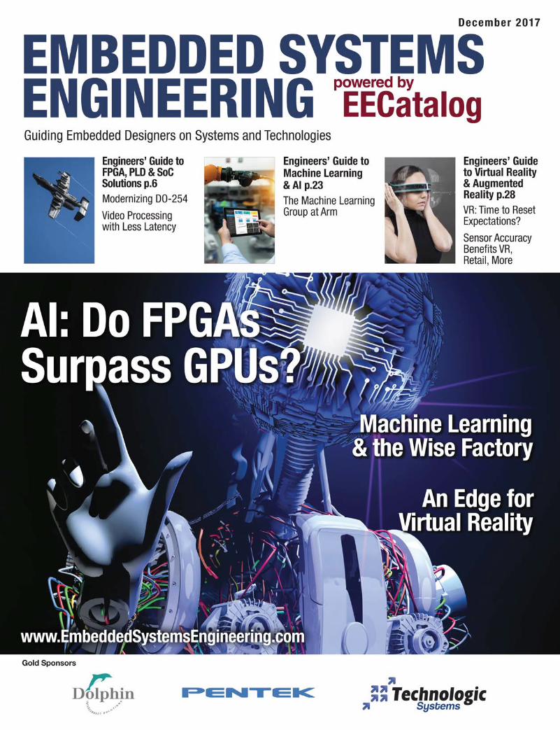
Intel’s Stratix 10 FPGA qualifies Intel as a large hardware supplier for
DNNs. Inevitably, we will see more from Intel as Altera IP is absorbed
and put to good use throughout Intel’s technologies. Microsoft is
betting on FPGAs for accelerating its AI cloud platform. According
to Doug Burger, Distinguished Engineer at Microsoft and former
Professor of Computer Sciences at the University of Texas in Austin,
“By attaching high-performance FPGAs directly to our data center
network, we can serve DNNs as hardware microservices, where a DNN
can be mapped to a pool of remote FPGAs and called by a server with
no software in the loop. This system architecture both reduces latency,
since the CPU does not need to process incoming requests, and allows
very high throughput, with the FPGA processing requests as fast as
the network can stream them.”7
FPGAS: FINE-GRAINED ACCELERATORSA 2014 white paper titled, A Reconfigurable Fabric for Accelerating
Large-Scale Datacenter Services (for which Burger is a contributing
author) states, “FPGAs are now powerful computing devices in their
own right, suitable for use as fine-grained accelerators.” The paper
also states, “Our study has shown that FPGAs can indeed be used to
accelerate large-scale services robustly in the data center. We have
demonstrated that a significant portion of a complex data center
service can be efficiently mapped to FPGAs, by using a low-latency
interconnect to support computations that must span multiple
FPGAs.”8 At Hot Chips, a symposium on high-performance chips,
Microsoft recently demonstrated the fruit of the above study, Project
Brainwave, on Intel’s new 14nm Stratix 10 FPGA.
One of the methods that Microsoft employs in tuning data centers
for performance is to batch requests. Batching means breaking up a
request into smaller pieces and feeding them to a processor to improve
hardware utilization. However, batching is not effective for real-time
AI since eating “one bite at a time” can cause latency. To combat latency
issues with batched requests, Brainwave employs what Microsoft
calls “persistent” neural nets. Thus, when a single request arrives, all
resources (compute units and on-chip memories) are used to process
the request; no batching is required.
7. Burger, Doug. “Microsoft Unveils Project Brainwave for Real-Time AI.” Microsoft Research, Microsoft, 22 Aug. 2017, www.microsoft.com/en-us/research/blog/microsoft-unveils-project-brainwave/.
8. Putnam, Andrew, et al. “A Reconfigurable Fabric for Accelerating Large-Scale Datacenter Services.” IEEE Micro, vol. 35, no. 3, 2015, pp. 10–22., doi:10.1109/mm.2015.42.
Figure 6: The Intel® Stratix® 10 FPGA chip. (Source: Intel)
What if a large model cannot fit in one FPGA? Brainwave accommo-
dates large models at a scale of persistency that expands to the entire
data center. Massive numbers of FPGAs form a collaborative, persis-
tent DNN hardware microservice that enable scale-out of models,
performing at ultra-low latencies. Inter-layer pipeline parallelism
facilitates the data center network, and FPGAs communicate directly
(at less than 2μs/hop).7 Therefore, DNN hardware microservices are
shared by all FPGAs (Figure 1).
Intel FPGAs accelerate DNN workloads. Intel has plans for pre-config-
ured, Intel FPGA algorithms for licensed customer use. To learn more
about Project Brainwave, see Microsoft’s Research Blog at microsoft.
com. To learn more about Machine Learning starting with the basics,
visit Intel’s Nervana™ AI Academy.
Lynnette Reese is Editor-in-Chief, Embedded Systems Engineering, and has
been working in various roles as an electrical engineer for over two decades.
She is interested in open source software and hardware, the maker movement,
and in increasing the number of women working in STEM so she has a greater
chance of talking about something other than football at the water cooler.

21www.eecatalog.com/fpga FPGA Boards
CONTACT INFORMATION
engineers guide to FPGA, PLD & SoC Solutionsengineers guide to FPGA, PLD & SoC Solutions
Pentek
Model 71862 4-Channel 200 MHz A/D with Multiband DDCs, Kintex UltraScale FPGA - XMC Module Supported FPGA / PLDs: Kintex UltraScale FPGA
Model 71862 is a member of the JadeTM family of high-performance XMC modules. The Jade architecture embodies a new streamlined approach to FPGA-based boards, simplifying the design to reduce power and cost, while still providing some of the highest- performance FPGA resources available today.
Designed to work with Pentek’s new NavigatorTM Design Suite of tools, the combination of Jade and Navigator offers users an efficient path to developing and deploying FPGA-based data acquisition and processing.
The 71862 is a multichannel, high-speed data converter with programmable DDCs (digital downconverters). It is suitable for connection to HF or IF ports of a communications or radar system. Its built-in data capture feature offers an ideal turnkey solution as well as a platform for developing and deploying custom FPGA-processing IP. It includes four A/Ds, a complete multiboard clock and sync section and a large DDR4 memory. In addition to supporting PCI Express Gen. 3 as a native interface, the Model 71862 includes optional high-bandwidth connections to the Kintex UltraScale FPGA for custom digital I/O.
FEATURES & BENEFITS
◆ Complete radar and software radio interface solution
◆ Supports Xilinx Kintex UltraScale FPGAs
◆ Four 200 MHz 16-bit A/Ds
◆ Four wideband DDCs
◆ 32 multiband DDCs (digital downconverters)
TECHNICAL SPECS
◆ 5 GB of DDR4 SDRAM
◆ Sample clock synchronization to an external system reference
◆ LVPECL clock/sync bus for multimodule synchronization
◆ PCI Express (Gen. 1, 2 & 3) interface up to x8
◆ VITA 42.0 XMC compatible with switched fabric interfaces
PentekOne Park Way, Upper Saddle River, NJ 07458USATel: (201)818-5900Fax: (201) [email protected]://www.pentek.com/go/emfpgae71862
APPLICATION AREASAerospace/Defense, Automotive, Broadcast, Consumer, Data Processing and Storage, Industrial Automation, Medical Imaging, Wired Communcations, Wireless Com-munications, Communications
AVAILABILITYContact Pentek for availability
Boa
rds
and
Kits B
oards and Kits
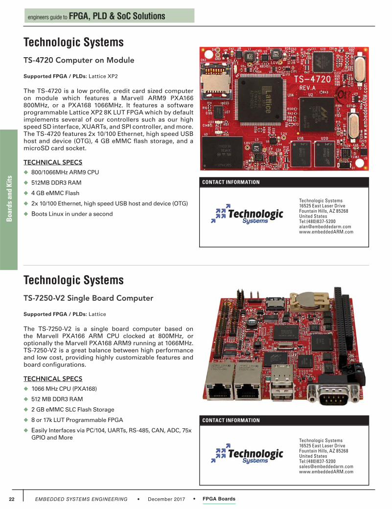
December 201722 FPGA Boards
CONTACT INFORMATION
engineers guide to FPGA, PLD & SoC Solutionsengineers guide to FPGA, PLD & SoC Solutions
CONTACT INFORMATION
Technologic Systems
Technologic Systems
TS-4720 Computer on Module Supported FPGA / PLDs: Lattice XP2
The TS-4720 is a low profile, credit card sized computer on module which features a Marvell ARM9 PXA166 800MHz, or a PXA168 1066MHz. It features a software programmable Lattice XP2 8K LUT FPGA which by default implements several of our controllers such as our high speed SD interface, XUARTs, and SPI controller, and more. The TS-4720 features 2x 10/100 Ethernet, high speed USB host and device (OTG), 4 GB eMMC flash storage, and a microSD card socket.
TECHNICAL SPECS
◆ 800/1066MHz ARM9 CPU
◆ 512MB DDR3 RAM
◆ 4 GB eMMC Flash
◆ 2x 10/100 Ethernet, high speed USB host and device (OTG)
◆ Boots Linux in under a second
TS-7250-V2 Single Board Computer Supported FPGA / PLDs: Lattice
The TS-7250-V2 is a single board computer based on the Marvell PXA166 ARM CPU clocked at 800MHz, or optionally the Marvell PXA168 ARM9 running at 1066MHz. TS-7250-V2 is a great balance between high performance and low cost, providing highly customizable features and board configurations.
TECHNICAL SPECS
◆ 1066 MHz CPU (PXA168)
◆ 512 MB DDR3 RAM
◆ 2 GB eMMC SLC Flash Storage
◆ 8 or 17k LUT Programmable FPGA
◆ Easily Interfaces via PC/104, UARTs, RS-485, CAN, ADC, 75x GPIO and More
Technologic Systems16525 East Laser DriveFountain Hills, AZ 85268United StatesTel:(480)[email protected]
Technologic Systems16525 East Laser DriveFountain Hills, AZ 85268United StatesTel:(480)[email protected]
Boa
rds
and
Kits B
oards and KitsB
oard
s an
d Ki
ts Boards and Kits

23
engineers guide to Machine Learning & AIengineers guide to Machine Learning & AI
www.eecatalog.com/machine-learning-ai
Beyond Automation: Building the Intelligent FactoryWhy the fate of factories and that of machine learning are intertwined.
Factories already have a lot in common with living
beings. They consume raw materials, require
energy, and have interlocking systems that all move in
a complex choreographed dance toward a shared goal.
Automation and computationally driven designs have
given us factory equipment that can perform repetitive
tasks with some variation based on operating condi-
tions and control signals.
But today’s factories can’t learn from their own mis-
takes, innovate autonomously, or teach themselves how
to optimize existing processes. That day is coming soon,
on a wave of machine learning that will drive the intel-
ligent factory of the near future.
Machine learning, combining distributed artificial
intelligence (AI), advanced sensors, and precision
robotics, is taking manufacturing into Industry 4.0.
It will be the fourth major era for manufacturing, fol-
lowing steam power, assembly lines, and automation.
CRUCIAL TECHNOLOGIES FOR THE INTELLIGENT FACTORYA number of significant advances are coming together
at the right time to make learning machines and intel-
ligent factories a reality. Wireless networking meshes
have reached a degree of speed and reliability such that
hundreds or even thousands of devices in a single fac-
tory can quickly and safely exchange information with
each other and with central data stores. Data mining
and analysis have advanced to help both human and AI
analysts find patterns hidden in the records, uncover
buried inefficiencies, and drive errors out of the work-
flow. Cloud technologies can store untold amounts of
data and perform constant analysis. And small ultra-
low-power networked sensors are capable of accurate
measurements well below 1mm and can distinguish
between materials such as plastic, drywall, and fabric.
Meanwhile, the huge investment in self-driving automobiles ben-
efits manufacturing with machine-vision breakthroughs, making
computers better than ever at recognizing objects and correctly
manipulating them. Computationally powerful but energy-efficient
multicore processors are small and affordable, and can be programmed
and repurposed by a wide range of coders worldwide. All of these ele-
ments are the building blocks of automated systems that will guide,
control, and educate the next generation of manufacturing capital.
HOW DATA BECOMES WISDOM IN THE INTELLIGENT FACTORYFor decades, data has been essential to safe and efficient operations
in any factory. Human operators already collect and analyze raw facts
and figures about inputs, outputs, waste, duty cycles and mechanical
failures. Advances in AI and big data processing make it possible to
create machines that cannot only generate more raw data, but can
also process the data into meaningful information, understanding
its content and applying that information as learned wisdom. These
machines will come together in intelligent factories and learn how to
avoid mistakes, correct imbalances, and improve processes.
Figure 1: A self-controlled machine acts based on wisdom distilled from lower levels, ultimately arising from massive amounts of data.
By Matthieu Chevrier and Tobias Puetz, Texas Instruments, Inc.
Matthieu Chevrier
Tobias Puetz

December 201724
engineers guide to Machine Learning & AIengineers guide to Machine Learning & AI
Today’s “smart” machines are only as adaptable as their pro-
gramming. Even a thorough coder cannot account for all of the
contingencies and variations a typical factory environment can
face. Wear and tear; variation in raw material quality; and environ-
mental factors like temperature, dust and grime can cause yields to
fall and components to fail, forcing costly slowdowns, repairs, and
adjustments.
With access to massive cloud data storage and computation, as well
as high-speed integrated processors, machines can start learning
from conditions as they occur. Distributed intelligence networks can
analyze every robot’s position and activity and every sensor’s report
on temperature, proximity, orientation, chemical composition, dis-
tance, and more.
Instead of just collecting data for later analysis, intelligent factories
will be able to apply AI to reach conclusions, make informed judg-
ments, and take corrective action. Robots will compensate for drift as
parts heat up or bearings wear down. Chemical control systems will
optimize recipes as conditions change, analyzing slight variances in
supply batches. Re-tuned and synchronized motors will work more
efficiently on cooperative jobs.
THE IMPACT OF THE INTELLIGENT FACTORYWhen they do come online, intelligent factories will become a new
engine of growth and profitability as self-healing, self-improving
centers of innovation. Manufacturing excellence in the Industry
4.0 world will belong to those who give their machines the data and
resources they need to perceive and report on the work they are doing,
with enough computational heft to translate that data into wisdom
and act automatically.
Combining AI with advances in both machine vision and voice-acti-
vated agents will make robots not only more powerful and productive,
but also safer and more reliable.
The intelligent factory doesn’t mean the end of human labor. In fact,
industrial intelligence could enable people and large-scale robots to
work together much more closely. Instead of being separated by safety
barriers, intelligent factory robots will be able to automatically detect
people nearby and adapt their own work to take greater precautions.
As the safety barriers around robots shrink or come down entirely,
further work on power conditioning and signal isolation will ensure
that robots have steady and reliable power sources that pose little risk
to people and other machinery in proximity.
We’ve yet to imagine the impact of intelligent factories. No one could
have invented Kanban or computer numerical control (CNC) without
first seeing an assembly line. In the same way, it’s safe to say that many
of the processes uniquely well-suited to intelligent factories won’t be
invented until the machines themselves start coming online. Human
imagination, unbounded by the need to rigidly program robots for
specific tasks and contingencies, will play a huge role in shaping the
increasingly complex mechanical, chemical, and biological products
made possible by intelligent factories.
Matthieu Chevrier is Systems Manager, PLC systems. Chevrier leads the
system team based in Freising Germany, which supports a WW base of
PLC (Programmable Logic Controllers) customers. He brings to his role his
extensive experience in embedded system designs in both hardware (power
management, mixed signal, and so on) and software (such as low-level
drivers, RTOS, and compilers). He earned his master of science in electrical
engineering (MSEE) from Supélec, an Ivy League university in France.
Chevrier holds patents from IPO, EPO, and USPTO.
Tobias Puetz is a Systems Engineer in the Texas Instruments Factory Automa-
tion and Control team, where he is focusing on Robotics and Programmable
Logic Controllers (PLCs). Puetz brings to this role his expertise in various
sensing technologies, power design, and wireless charging as well as software
design. He earned his master’s degree in electrical engineering and information
technology at the Karlsruhe Institute of Technology (KIT), Germany in 2014.

25
engineers guide to Machine Learning & AIengineers guide to Machine Learning & AI
www.eecatalog.com/machine-learning-ai
The Machine Learning Group at Arm An Interview with Jem Davies, Arm Fellow and Arm’s new VP of Machine Learning.
Arm has established a new Machine Learning (ML)
group. Putting this within context, machine
learning is a subset of AI, and deep learning is a subset
of ML. Neural networks are a way of organizing com-
putational capabilities that are particularly effective
for delivering the results that we see with machine
learning. With machine learning, computers “learn”
rather than get programmed. Machine learning is
accomplished by feeding an extensive data set of
known-good examples of what the computer scientist
wants to see from the machine.
Arm has published some of its viewpoints about Artifi-
cial Intelligence (AI) online.
According to Jem Davies, Arm Fellow and Arm’s new VP of Machine
Learning, Client Line of Business, machine learning is already a
large part of video surveillance in the prevention of crime. Davies’
prior role as general manager and Fellow, Media Processing Group
at Arm, is an excellent segue into ML, as Graphic Processing Units
(GPUs) hold a primary role in accelerating the computational algo-
rithms needed for ML. ML requires large amounts of good data and
computational power that is fast at processing repetitive algorithms.
Accelerators like GPUs and now FPGAs are used to off-load CPUs so
the entire ML process is accelerated.
Davies is the kind of good-humored, experienced engineer whom
everyone wants to work with; his sense of humor is just one tool in
his arsenal for encouraging others with an upbeat attitude. I had an
opportunity to meet with Davies at Arm TechCon. Edited excerpts of
our interview follow.
Lynnette Reese (LR): Artificial Intelligence (AI) as a science has been
around for a very long time. What attributes in improved technology
do you think contributed the most to the recent maturing in AI? Is it
attributed to the low cost of compute power?
Jem Davies: Really, it’s the compute power
that’s available at the edge. In the server,
there’s no real change, but the compute power
available at the edge has transformed the last
five years, so that’s made a huge difference.
What’s fired up interest in the neural network
world is the availability of good quality data.
Neural networks provide a technique that’s
more than 50 years old, what we’ve got now
is the training data, good, quality, correlated data. So for example,
the one that sort of drove it initially was image recognition. In
order to train a neural network to do image recognition, you have
to have vast quantities of images that are labeled. Where are you
going to find one of those? As it turns out, Google and Facebook
have all of your pictures. You’ve tagged all of those pictures, and
you clicked on the conditions that said they could do what they
Figure 1: Deep learning, using Neural Networks (NN), attempts to model real life with data using multiple processing layers that build on each other. Examples of algorithms integral to ML include Convolutional Neural Networks (CNNs), Recurrent Neural Networks (RNNs), and others. (Credit: Arm, Jem Davies)
By Lynnette Reese, Editor-in-Chief, Embedded Systems Engineering
Jem Davies, Arm

December 201726
engineers guide to Machine Learning & AIengineers guide to Machine Learning & AI
wanted with them. The increasing capability of computing, par-
ticularly in devices, has led to the explosion in data.
LR: You said that the explosion of data is the impetus for machine
learning, and this is clear with image recognition, perhaps, but where
else do we see this?
Davies: The computational linguists are having a field day. Nowadays
we have access to all sorts of conversations that take place on the
internet. You have free, easy access to this data. You want to work out
how people talk to each other, look on the internet. If you are trying to
work out how people talk to each other, look on the web. And it turns
out that they do it in all sorts of different languages, and it’s free to
take. So, the data is there.
LR: So, applying successful ML to any problem first requires good data?
Davies: If you haven’t got the data, it’s difficult to get a neural net-
work algorithm. They are working on that; there is research being
done to work using much smaller amounts of training data, which
is interesting because it opens up training at the device level. We are
doing training on-device now but in a relatively limited way; but you
don’t need six trillion pictures of cats to accomplish cat identification.
LR: In your Arm talk about Computer Vision last year you said there
were 6 million CCTVs in the U.K. What do you imagine AI will be doing
with images CCTV 20 years from now? For instance, do you perceive
that we can combat terrorism much more efficiently?
Davies: It is being done today. We are analyzing gait, suspicious
behavior; there are patterns people have that give themselves away.
This is something an observational psychologist already knows.
People give themselves away by the way they stand; the way they hold
themselves.
LR: What about sensing beyond visual recognition? For example, can
you use an IR sensor to determine whether a facial prosthesis is in use,
for example?
Davies: When engineering moves beyond the limited senses that
humans possess, you can throw more information at the problem.
Many activities work much better using IR than in the visible spec-
trum. IR poses fewer issues with shadows, for instance. One example
of challenges we face with a security camera is that the camera might
have to cover an area where the sun is streaming down, and there’s
a shadow at the other end of the frame. If you are tracking someone
from one side to the other of the frame, shadows can interfere with
obtaining consistent detail in such situations. Move that to the IR
domain, and it gets a whole lot easier. But why stop there? You can add
all sorts of other things to it as well. Why not add radar, microwaves?
You can do complete contour mapping.
LR: So, you could get very detailed with this? Adding additional sen-
sors can give more data.
Davies: Yes, sensor fusion is the way forward. We [humans] are
adding together the input from all our senses all the time. And our
brains sometimes tell us, “That input doesn’t fit, just ignore it.” I can
turn my head one way and think I can still see someone in my periph-
eral vision. But actually, you can’t. The spot right in front of you is the
area that you can see in any detail. The rest is just your brain filling
things in for you.
LR: What’s Arm doing to innovate for AI?
Davies: We are doing everything; hardware, software, and working
with the ecosystem. If you look at hardware, we are making our
existing IP, our current processors better at executing machine
learning workloads. We are doing that for our CPUs and our GPUs. On
the interconnect side, things like DynamIQ [technology], enable our
partners to connect other devices into SoCs containing our IP. This is
a considerable amount of software because people do not want to get
deep into the details.
If you look at the Caltrain example, where an image recognition
model for trains was developed with data from Google images and
used on a 32-bit Arm-based Raspberry Pi, it’s becoming quite easy to
apply ML techniques. He just downloaded stuff off the web; he didn’t
know anything about it. He’s not an image recognition specialist, he
doesn’t know anything about neural networks, and, why should he?
If we [Arm] do our jobs properly, if we provide the software to people,
it just works. It turns out there’s a lot of software involved; probably
half my engineers are software engineers. The Arm compute library,
is given away [as] open source; it has optimized routines to do all the
things that go into machine learning. That is what powers the imple-
mentations on our devices. Google’s Tensorflow, Facebook’s Caffe,
and others plug into that, and so you end up with force multiplier
effect. We do the work, give it to the ecosystem, and Facebook has
now got millions of devices that are optimized to run on Arm CPUs
and Arm Mali GPUs. As you can see, there’s a lot of hardware devel-
opment, software development, and a significant amount of working
with the ecosystem. Everybody’s getting involved.
LR: What can you tell me about Arm’s new Machine Learning busi-
ness? Do you have any industry numbers?
Davies: Industry numbers are hard to get. What I will say is that it’s
going to be huge. It’s going to affect everything we do. One of the rea-
sons why we formed the machine learning business as it is, is that it
cuts across all new lines of business.
LR: Not that you should take sides, but what would you say about
using FPGAs vs. GPUs in AI?
Davies: Arm doesn’t take sides. Arm always plays both sides. FPGAs
are flexible; you can reconfigure the hardware to great benefit. But that
comes at the cost of much less density and much more power. People
[physically] get burnt touching an FPGA. For us, it’s a trade-off. If you
can implement something in an FPGA that’s absolutely, specifically tai-

27
engineers guide to Machine Learning & AIengineers guide to Machine Learning & AI
www.eecatalog.com/machine-learning-ai
lored to that problem. Presumably, it will be more efficient. But executing
on an FPGA…an FPGA is bigger, much more expensive, and uses more
power. Which way does that balance come down? It’s a different problem,
as it comes down to it. Pretty much for anything battery powered, the
answer is that FPGAs are a bust in that space. FPGAs don’t fit there; not
in small, portable electronic devices. For environments that are much
bigger, less power constrained, maybe there’s a place for it. However,
note that both Altera and Xilinx have products with Arm cores now.
LR: What would you say to young engineers starting out today that
want to go into Machine Learning?
Davies: “Come with us, we are going to change the world,” which
is precisely what I said in an all-hands meeting with my group just
last week. And I don’t think that’s too grand. Look at what Arm did
with graphics. We started a graphics business in 2006; we had zero
market share. Yet our partners shipped over a billion chips last year
containing Mali Arm GPUs.
LR: Billions of people are tapping on their devices using Arm’s technology.
Davies: Yes. If I look back on what we have achieved at Arm, the
many hundreds of people doing this, you can easily say that Arm has
changed the world.
LR: So, Arm is not a stodgy British company? Everyone needs good
talent, and Arm is changing the way we live?
Davies: Absolutely, we are a talent business. Don’t tell the accoun-
tants, but the assets of the company walk out the door every night. If
you treat people well, they come back in the next morning.
LR: It sounds like Arm values employees very much.
Davies: Well, we definitely try to. Clearly, as any company, we occa-
sionally get things wrong, but we put a lot of effort into looking after
people because together we make the company. As with any company,
our ambition is limited by the number of people we have. Effectively,
we are no longer limited by money [due to Softbank’s vision upon
acquiring Arm].
LR: So now you can build cafeterias with free food and busses to carry
employees around?
Davies: Right, I am still waiting for my private jet…but seriously,
that’s what I was talking about, that we are changing the world. I
think [new graduates] would want to be part of that.
Lynnette Reese is Editor-in-Chief, Embedded Systems Engineering, and
has been working in various roles as an electrical engineer for over two
decades. She is interested in open source software and hardware, the
maker movement, and in increasing the number of women working in
STEM so she has a greater chance of talking about something other than
football at the water cooler.
Machine Learning and AI ONLINE
Explore...➔ Top Stories and News
➔ White Papers
➔ Expert Opinions (Blogs)
➔ Exclusive Videos
➔ Valuable Articles
Machine Learning and AI Quarterly Report email newsletter
www.eecatalog.com/machine-learning-ai
www.eecatalog.com/machine-learning-ai

December 201728
engineers guide to Virtual Reality & Augmented Realityengineers guide to Virtual Reality & Augmented Reality
The Future of VR Depends on Lessons from Its PastWhy we need to reset our expectations of what technology can deliver
today if we want VR to be successful tomorrow.
Virtual reality (VR) stands at a critical juncture.
Down one path are consumers clamoring for pow-
erful, transformative devices that will open up a new
age of virtual immersion. On the other, developers,
designers, and engineers continue to grapple with a
long list of technology limitations that frustrate the
ideal wearable headset design.
WHAT WE NEED TO MAKE VR SUCCESSFULVR requires a highly complex blueprint of features and
functions, mimicking the human brain—the most com-
plicated of which is spatiotemporal orientation. VR must
persuade our minds in multiple ways (visually, aurally,
with scale and context) to believe that the digital is
reality, or at least a very good simulation of reality.
To be clear, VR will transform our world. According to
Orbis Research, spending on VR technology (indepen-
dent from augmented reality) is expected to surpass
$40 billion by 2020. Research firm IDC also reports
that spending on VR systems is forecast to be greater
than AR-related spending in 2017 and 2018. VR will
transform how we learn, play, create, build, manage,
market and interact. Even how we compete.
A CANDID ASSESSMENT OF VIRTUAL REALITY TODAYWe can trace the modern concept of consumer VR
technology to the 1990s, when the Sega VR-1 motion
simulator was released. It was (by today’s standards) a
crude mash-up of visor, stereo headphones and sensors
that roughly tracked and responded to the wearer’s
head movements.
Fast forward to 2010, when the first personal virtual
reality headset prototype, the Oculus Rift, emerged
on Kickstarter. It featured a breakthrough 90-degree
field of vision (FOV) and was later purchased by Face-
book, setting off an avalanche of VR investment and developments
by competitive technology companies. This came with projections
that the ultimate consumer VR experience was mere months away.
So, what keeps us from delivering a mass consumer, high-end stand-
alone VR experience? Three key issues:
Tethered headset and latency. A robust and immersive VR
system demands a powerful computer with a fast graphic card,
which today is only possible via a physical connection to a PC.
But, our relationship with mobile phones, tablets, laptops and
more has resulted in a consumer market that considers sta-
tionary technology archaic. Additionally, wearing a headset while
tethered to anything, as you try to move within your virtual envi-
ronment, is annoying at best—an immersion-killer at worst. In
addition, latency—image lag following a head motion—can be a
real cause for a flawed VR experience and the oft-mentioned (and
never popular) issue of VR motion-sickness.
Form factor. Never underestimate the importance of comfort,
fit and style—particularly in a product worn on the face. Lenses
need to align with every set of eyes; headphones need to fit
comfortably in the ear, and weight distribution, calculated for
comfort and overall size, all need to be taken into account. Right
now, 360-degree, fully occlusive VR headsets are very heavy.
We are essentially trying to package a high-powered computer
with rapid processing speed, high-resolution graphics, positional
audio, motion tracking and reasonable battery life into a cool-
looking pair of glasses.
Price. No VR system comes cheap. Facebook’s Oculus Rift headset
is currently $400, not counting the added cost of the computer
needed to power its virtual reality experiences and games—that’s
expensive, especially for the casual VR user (although the Oculus
Go costs $200). The highly touted HTC Vive runs about $600, and
the console Sony PlayStation VR about $400. The most widely
used mobile option (for those who already own a new Samsung
phone) is the Samsung Gear VR at about $130.
By Dr. John C.C. Fan, Kopin Corporation

29
engineers guide to Virtual Reality & Augmented Realityengineers guide to Virtual Reality & Augmented Reality
www.eecatalog.com/virtual-augmented-reality
Then there’s the accessories. For about
$299 (pre-order), TPCast’s wireless
adapter for HTC Vive establishes a wire-
less connection capable of transmitting a
2K resolution between the Vive’s hardware
and host PC, with less than two millisec-
onds latency. Also gathering steam (and
crowdfunding on Kickstarter) is the $800,
Shanghai-based Pimax 8K VR headset,
which features two 4K screens and a wire-
less transmission add-on similar to the
TPCast wireless upgrade kit.
SOLVING THE ISSUES: LESSONS FROM TECHNOLOGIES PAST As always, past technology evolutions and
milestones may influence the future of mass
consumer VR adoption.
First, consider the impacts of overcompli-
cated design. Consumers assume that a
completely immersive experience can be
crammed into a sleek pair of sunglasses. Not
true—yet. The reality is that features and
functionality come at the expense of size
and weight. If we are to look at technology
from a practical perspective, the military is
a prime example of delivering highly func-
tional, yet stripped-down, devices designed
to serve specific needs. Similarly, by scaling
back the bells and whistles, and delivering
disciplined products—manufacturers can
ease consumers into VR.
And by compromising some features, VR
can still deliver an adequately immersive
experience. This is not to say that VR
doesn’t have essential requirements, but
some functionality is more ‘ luxurious’
than others.
One example is the emphasis on wide FOV,
which makes the user feel more present
in the experience. But wide FOV requires
designers to use bigger displays and bigger
optics, making the headset very bulky. In
addition, magnifying display images with
insufficient resolution in pursuit of wide
FOV aggravates the “screen door effect”
(where individual pixels become so ampli-
fied as to be distracting to the experience).
At Kopin, we offer smaller size, but higher
resolution (2048 x 2048) OLED displays with
greater pixel density (3000 pixels per inch)
to mitigate the dreaded “screen door effect.”
Images are magnified and exaggerated using
stronger—but much thinner—lenses to
allow a very compact headset.
And while weight, comfort, and style will
make or break VR adoption and public accep-
tance—don’t forget price. For those of us old
enough to remember the Motorola DynaTAC
(brick) cell phone, you’ll also recall the ‘cringe’
factor associated with a device so large it was
obvious and obnoxious. But it was the price—
$3,995 ($9600 in 2016 dollars)—that kept it
from being a mass-market product. In 1996
Motorola unveiled the flip clamshell StarTAC
at the cost of $1000, and widespread consumer
adoption of the cell phone was born.
THE FUTURE OF VRSo, how does the industry extend the appeal
of existing VR technology to the masses while
encouraging innovation?
First, consumer onboarding to VR must be
made as easy and affordable as possible.
While the most immersive and hyper-realistic
experiences are still the domain of gamers,
securing a sophisticated VR system will set
them back $1000-1500.00. However, since
gamers are most likely to already possess the
core equipment, they are usually the first to
adopt VR technology. Luckily, most technolo-
gies go through natural price adjustments as
computer and device specs evolve to accom-
modate desired features.
Another lesson from the past is that,
eventually, dominant platforms emerge,
streamlining both hardware and software
development over time.
Critical to VR’s future success is form.
Knowing that today’s consumer expects
their communication and entertainment
devices to be portable and universally acces-
sible likely means standalone headsets will
win. But at the same time, wireless headsets
will need to be comfortable on many levels,
so weight, size and style will factor signifi-
cantly in whether a device becomes a novelty
or an integral part of everyday life.
So, although the tech limitations of today
are clear, VR is on the path to eventual mass
adoption. And while challenges like price,
ergonomics, low resolution, latency and even a
shortage of content, have slowed VRs integra-
tion into the mainstream, acknowledging these
obstacles assures us that fixes will surface.
When the stakes are this high, winners will
emerge in the race to transform how people
interact with the digital and physical worlds.
Dr. John C.C. Fan is the CEO and co-founder of
Kopin Corporation. For more information, please
visit Kopin’s website at www.kopin.com.

December 201730
engineers guide to Virtual Reality & Augmented Realityengineers guide to Virtual Reality & Augmented Reality
Extreme Sensor Accuracy Benefits Virtual Reality, Retail, and NavigationWhat minimizes lag that leads to VR “motion sickness,” explains why your store coupon app requires use
of your smartphone’s accelerometer, and keeps fitness trackers and cars on track even when GPS fails?
Good Virtual Reality (VR) is an immersive experience,
a simulated world with a hint of boundaries. Excel-
lent VR is closer to the real thing. VR technology has to
have a very high-density display with enough pixels to
make sure that VR can emulate real-life details. Spatial
stereo audio is also part of that immersive experience. That
is, audio should sound like it’s emanating from the same
place as the associated visual. Audio reception in a perfect
VR experience would include the Doppler Effect and other
physical vagaries of sound. Lastly, VR immersion should
include the ability for the user to intuitively interact with
the system, as you might in real life. However, VR has not
yet reached perfection in any of the above areas; with a
high level of visual detail, experientially accurate sound,
or the ability to interact naturally in a virtual world. Alas,
VR is still in the early days, causing “VR sickness” by
making many users nauseated; a sickness that’s mainly
due to a time lag of more than 20 ms, as the differences
in sensory inputs conflict with each other1. The latest VR
products have a lag delay of 6 to 10 ms, however, enabling
lengthier and more enjoyable VR experiences.
VR will show nothing in the user’s actual surroundings,
whereas Augmented Reality (AR) supplements the real-
world view, much like a heads-up display with an overlay
of information superimposed onto the user’s view of
actual surroundings. For developers, there’s a “spectrum
of immersion” in Virtual Reality (VR), depending upon
the technology that’s put into play. VR can be as simple
as sliding a smartphone into a Google cardboard device
that looks a bit like a View Master (a vintage stereoscopic
viewing toy), or VR can be quite immersive, with a 360°
headset, in-sync spatial audio, and controllers and sen-
sors for both hands and feet. People in the industry are
increasingly using the term “XR” to refer to “AR/VR.” A
more detailed look at the XR spectrum starts with VR and extends to AR
at the other end of the spectrum, with Mixed Reality (MR) existing as a
less confusing name for AR.
Micro Electro-Mechanical Systems (MEMS), a semiconductor tech-
nology used for creating tiny sensors such as accelerometers, gyroscopes,
magnetometers, and more, is in wide use in the XR market. A significant
player in the MEMS/sensor industry is InvenSense, now a part of TDK,
with a sizeable $368 million (USD) share in the 2016 MEMS market.
David Almoslino, Sr. Director Corporate Marketing at TDK InvenSense,
has an excellent handle on the XR industry since sensors play a critical
role in the outcome of the VR experience. Sensors do much more than
sensing at InvenSense, however, and are found in a majority of XR
headsets, controllers, and related peripherals. Sensors work in concert
to gather and synthesize data in what’s known as sensor fusion. As
Almoslino states, “HTC Vive has incorporated InvenSense technology
Figure 1: Excellent VR is an immersion experience. AR shares design challenges with VR such as latency and precise motion tracking. (Source: Qualcomm)
By Lynnette Reese, Editor-in-Chief, Embedded Systems Engineering
1. Mason, Betsy. “Virtual Reality Has a Motion Sickness Problem.” Science News, 8 Mar. 2017, www.sciencenews.org/article/virtual-reality-has-motion-sickness-problem.

31
engineers guide to Virtual Reality & Augmented Realityengineers guide to Virtual Reality & Augmented Reality
www.eecatalog.com/virtual-augmented-reality
for one-to-one tracking for
how the head is moving. At the
same time, HTC controllers
have our tracking ability with
InvenSense Inertial Measure-
ment Units in each controller.
All these sensors track and
communicate so that when you
are physically moving in a game,
the Inertial Measurement Unit
(IMU) recognizes the inputs
and keeps them all together so
that you can truly be immersed
in a game.” Gaming is just one
use for XR, however.
Augmented Reality (AR) is similar to VR but has the additional design
burden of a heads-up display and potentially more sensors that feed data
directly to the viewer. Many design challenges are shared. Improving the
level of visual detail in XR to perfectly emulate reality may require a dis-
play that nears the resolution of the human eye, requiring a high density
of pixels (≥2160 x 1080) and a frame per second (fps) rate of at least 60
fps. Field of View (FoV) should be at least 110°. High-performance com-
puting is required to render data with a high pixel density and frame
rate without adding lag, as the data processing burden is enormous. It
is crucial that data from motion sensors (also known as IMUs) in the
VR headset and hand controllers line up with the corresponding visual
display on the headset. If not, lag ensues.
REDUCING LAGHigh-performance computing aside, much of the work in lowering
lag resides in sensors. InvenSense is known for very accurate sensors.
Real-world sensing translates to analog input that requires filtering,
digitization, and additional processing, for which these sophisticated
sensors have integrated microprocessors to process and format data
before sending it to the main CPU.
Lars Johnsson, InvenSense’s Sr. Director of Product Marketing, explains
how InvenSense IMUs reduce lag and ease the developer experience. “The
sensors have integrated filtering with adjustable parameters that include
bandwidth and noise. When taking the signal from analog to digital,
there’s something called a Digital Motion Processor (DMP) that performs
post-processing for sensor fusion, which we offer at certain data and
sampling rates. Sensing followed by rapid conversion and post-processing
happens locally in our sensor so that when it reaches the rendering engine,
it is preprocessed. For VR, all developers have to do is say, ‘If the user looks
1° to the left and 10° up, here is what he should see,’ and the correct spot
just gets presented to the screen.” In other words, calculating vectors for
relational placement of the display in concert with the physical placement
of the headset is done for you.
The sum of the parts of XR add up to a very complicated but exquisitely
coordinated high-performance sensing and compute platform. Minutiae
do not burden developers when using smart sensors that include prac-
tical algorithms. Algorithms will vary for sensors in different locations.
As Nicolas Sauvage, InvenSense’s Sr. Director of Ecosystem, points out,
“Sensors in the headset are less likely to experience the kind of speed and
acceleration that hand controllers present. The performance of an IMU
in the hand controllers has different performance tradeoffs than an XR
headset.” InvenSense is tuned in to the finer details of VR design. Sauvage
goes on to explain, “We fine-tune the performance of our chips to take
advantage of these different performance trade-offs. Since your head
with the headset will never be as fast as your hands, we can smartly adjust
trade-offs in the acceleration of the head. Latency for motion sickness is
significant here, but may not be as important elsewhere.”
SENSORS COMBAT MOTION SICKNESSSensor accuracy plays a very large part in avoiding motion sickness due to
lag. There has to be a perfect alignment between where the user is looking
and where the VR rendering engine thinks the user is looking. Add the
rapid movement of two separate hand controllers and the action that’s
integrated into the picture within the VR game, and you have a recipe for
disaster without good sensors. Johnsson goes on to say, “With respect to
having very low noise and very high-temperature stability, as the elec-
tronics quickly warm up, you don’t want signals to drift as they react to
a temperature change. We compensate for these types of things, as they
affect accuracy and can create lag.” InvenSense sensors are in the Oculus
Rift, Microsoft HoloLens, HTC Vive, and numerous other XR products.
AUGMENTED REALITY Augmented Reality requires an informative overlay onto a display,
whether projected inside a Head-Mounted Display (HMD) visor or in a
heads-up display in a car. A well-known example of AR/MR is Pokémon
Go, which is played on a smartphone. In the game, Pokémon characters
are superimposed on a smartphone screen as captured by the camera
in various GPS locations. Other uses for AR include training and as a
productivity enhancer. One lesser-known benefit of VR is that users
are somewhat forced to focus on the content that’s strapped to their
head. Unlike with a TV, VR would make it more difficult for users to
look at their smartphones during advertising. Training employees with
VR as a medium ensures that they cannot do something else while
Figure 2: Six Degrees of Freedom (DOF) offers more than orientation (3 DOF), but will track your location as you physically move around. Latency (lag) adds up as the XR system collects and processes huge amounts of data. (Source: TDK InvenSense.)

December 201732
engineers guide to Virtual Reality & Augmented Realityengineers guide to Virtual Reality & Augmented Reality
in the training session, for instance.
Boeing found that AR, as tested in
a manufacturing setting against a
control group, increased productivity
by 25%. According to the Harvard
Business Review, AR improved pro-
ductivity significantly in a warehouse.
“At GE Healthcare a warehouse worker
receiving a new picklist order through
AR completed the task 46% faster than
when using the standard process, which
relies on a paper list and item searches
on a workstation2. Additional cases from GE and several other firms
show an average productivity improvement of 32%.”
A three-axis accelerometer measures movement in three dimen-
sions. Adding other sensors adds additional axes for acuity with
more data. In the industry, it’s common to refer to a pressure sensor
as an additional axis, for instance, because the sensor measures
height in the air based on air pressure, not motion. Fusing the
inputs gives more accurate data. A nine-axis sensor would include
three degrees of freedom each from an accelerometer, a gyroscope,
and magnetometer. Software algorithms complement sensor fusion.
One prominent example in navigational mapping uses GPS as well as
six-, seven-, or nine-axis IMUs that continuously measure orienta-
tion changes and speed. These IMUs keep travelers on track when
GPS fades. For example, navigating a tunnel with a highly accu-
rate IMU will accurately track a car’s progress without GPS, since
error accumulates on a minuscule level when you have high levels
of accuracy. The InvenSense Positioning Library (IPL) algorithms
can implement tracking to complement navigation when GPS goes
missing in an urban canyon. Other use cases include wearables that
may incorporate power-hungry GPS only intermittently, preserving
battery power while keeping true to course. Have you ever wondered
why a smartphone application for in-store coupons would need
permissions for accessing your gyroscope/accelerometer? Retail use
cases include smartphone applications that can accurately track and
monitor a person’s travel inside a store using a highly accurate six-
axis IMU. Tracking can easily include how long a person stays in a
particular location. With a standard store layout and accurate posi-
tion tracking triggered by a single Bluetooth beacon as users enter
the store and open their coupon apps, data can reveal information on
shoppers. A shopper might get a pop-up offer on their smartphone
app for a discount on Snuggies after walking away from a Snuggies
display where they lingered a little too long. This accurate tracking is
done without expensive video cameras. It’s easy to see that extremely
accurate sensors are affecting more than VR.
WHERE IS VR HEADED?The global VR Head-Mounted Display market is projected to
increase to around 90 million units per year by 2021. VR has some
challenges with fragmentation in platforms for developers. VR
content is challenging across a fragmented landscape of various
platforms with varying numbers of controllers and no one unifying
standard, at least not one that’s been widely adopted yet, similar to
how USB solved the problem for connectors. VR systems can come
with up to two controllers, affecting the application of gameplay
with each choice. Pricing puts the best VR systems out of reach for
much of the existing gaming market. A lack of good content comes
with the territory for a VR market fragmented by many platforms,
making it that much more difficult for developers to create content
that sells in volume across many platforms. These challenges are
being solved, as many see XR as a wondrous experience and a pro-
ductivity boon for a manufacturing sector with rising job openings
and falling hiring rates.
The highly accurate sensors used in XR translate well to several other
segments. As for InvenSense, the TDK purchase was a good thing.
Almoslino’s perspective is seasoned by years of experience in sensors,
where InvenSense excels. “InvenSense has had sensor success in the
consumer products area and TDK in industrial, and together they
complement each other. The automotive sector is going to be our next
big growth scene.”
AR is already making significant headway into increasing productivity
of workers in warehouse “pick and pack” activities. Transportation
industries that include trains, busses, and automobiles will benefit from
previously unaffordable, augmented heads-up displays (HUDs) that a
decade ago were only available in sectors big budgets and critical impor-
tance, such as in military cockpits. It is without doubt that XR will have
a significant impact on economies world-wide by increasing productivity
and decreasing accidents.
Lynnette Reese is Editor-in-Chief, Embedded Systems Engineering, and has
been working in various roles as an electrical engineer for over two decades.
She is interested in open source software and hardware, the maker movement,
and in increasing the number of women working in STEM so she has a greater
chance of talking about something other than football at the water cooler.
Figure 3: The global VR Head-Mounted Display market is projected to increase to around 90 million units per year by 2021. (Source: ABI Research)
2. https://www.youtube.com/watch?v=AwZ3yYydOH4&feature=youtu.be


![PhD Research Proposal A SAT+CAS system for checking math ...cbright/talks/proposal-slides.pdf · Motivation TheresearchareasofSMT[SAT-Modulo-Theories] solvingandsymboliccomputationarequite](https://static.fdocuments.net/doc/165x107/5cc7a21b88c99360678c337b/phd-research-proposal-a-satcas-system-for-checking-math-cbrighttalksproposal-slidespdf.jpg)


