
Electrostatic Properties of Ideal ... -...
15
DOI: 10.1002/adma.200701681 Electrostatic Properties of Ideal and Non-ideal Polar Organic Monolayers: Implications for Electronic Devices** By Amir Natan, Leeor Kronik,* Hossam Haick, and Raymond T. Tung 1. Introduction Molecular electronics, which involves the use of molecules and molecular assemblies as passive and active electronic de- vices, [1–3] has attracted much attention because it allows for the design and realization of novel nano-scale devices. A re- lated, but conceptually different, approach is to use molecular functionality to influence and control the characteristics of otherwise conventional electronic devices. [4,5] In this way, one can benefit from both the inherent design flexibility offered by molecules and the maturity and robustness of semiconduc- tor-based electronic devices, so as to enjoy the best of both worlds. For example, hybrid structures comprised of molecu- lar layers adsorbed on semiconducting or metallic substrates have been shown to exhibit novel electro-optical [6,7] and mag- netic [8,9] properties that the individual components do not nec- essarily possess on their own. Here, we focus on one specific strategy for modifying elec- tronic device properties with molecules, viz. use of polar monolayers at surfaces and interfaces. [4,5,10] Generally, a polar monolayer introduces a net electrical dipole perpendicular to the surface/interface. [10] This results in a potential shift that modifies the work function and electron affinity at a surface PROGRESS REPORT Adv. Mater. 2007, 19, 4103–4117 © 2007 WILEY-VCH Verlag GmbH & Co. KGaA, Weinheim 4103 Molecules in (or as) electronic devices are attractive because the variety and flexibil- ity inherent in organic chemistry can be harnessed towards a systematic design of electrical properties. Specifically, monolayers of polar molecules introduce a net di- pole, which controls surface and interface barriers and enables chemical sensing via dipole modification. Due to the long range of electrostatic phenomena, polar monolayer properties are determined not only by the type of molecules and/or bonding configuration to the substrate, but also by size, (dis-)order, and adsorption patterns within the monolayer. Thus, a comprehensive understanding of polar monolayer characteris- tics and their influence on electronic devices requires an approach that transcends typical chemical designs, i.e., one that incorporates long-range effects, in addition to short-range effects due to local chemistry. We review and explain the main uses of polar organic monolayers in shaping electronic device properties, with an emphasis on long-range cooperative effects and on the differences between electrical properties of uniform and non-uniform monolayers. – [*] Dr. L. Kronik, A. Natan Department of Materials and Interfaces Weizmann Institute of Science Rehovoth 76100 (Israel) E-mail: [email protected] Dr. H. Haick Department of Chemical Engineering and Russell Berrie Nanotechnology Institute Technion – Israel Institute of Technology Haifa 32000 (Israel) Prof. R. T. Tung Department of Physics Brooklyn College of the City University of New York Brooklyn, NY 11210 (USA) [**] We thank Ron Naaman (Weizmann Institute), David Cahen (Weiz- mann Institute), Dudi Deutsch (Weizmann Institute), and Abraham Nitzan (Tel Aviv University) for many illuminating discussions. Work in Rehovoth was supported by the “Bikura” track of the Israel Science Foundation, the Gerhard Schmidt Minerva Center for Su- pra-Molecular Architecture, and the historic generosity of the Har- old Perlman family. LK holds the Delta Career Development Chair and is an ad personem member of the Lise Meitner Center for Com- putational Chemistry. HH holds the Horev Chair for Leaders in Science and Technology and acknowledges a Marie Curie Excellence Grant of the EC’s FP6 and the Russell Berrie Nanotechnology Insti- tute for support. RTT gratefully acknowledges financial support from the National Science Foundation (DMR-0706138). HH and RTT also thank the US-Israel Binational Science Foundation for financial sup- port.
Transcript of Electrostatic Properties of Ideal ... -...

DOI: 10.1002/adma.200701681
Electrostatic Properties of Ideal andNon-ideal Polar Organic Monolayers:Implications for Electronic Devices**
By Amir Natan, Leeor Kronik,* Hossam Haick,and Raymond T. Tung
1. Introduction
Molecular electronics, which involves the use of moleculesand molecular assemblies as passive and active electronic de-vices,[1–3] has attracted much attention because it allows forthe design and realization of novel nano-scale devices. A re-lated, but conceptually different, approach is to use molecularfunctionality to influence and control the characteristics ofotherwise conventional electronic devices.[4,5] In this way, onecan benefit from both the inherent design flexibility offeredby molecules and the maturity and robustness of semiconduc-tor-based electronic devices, so as to enjoy the best of bothworlds. For example, hybrid structures comprised of molecu-lar layers adsorbed on semiconducting or metallic substrateshave been shown to exhibit novel electro-optical[6,7] and mag-netic[8,9] properties that the individual components do not nec-essarily possess on their own.
Here, we focus on one specific strategy for modifying elec-tronic device properties with molecules, viz. use of polarmonolayers at surfaces and interfaces.[4,5,10] Generally, a polarmonolayer introduces a net electrical dipole perpendicular tothe surface/interface.[10] This results in a potential shift thatmodifies the work function and electron affinity at a surface
PRO
GRES
SREP
ORT
Adv. Mater. 2007, 19, 4103–4117 © 2007 WILEY-VCH Verlag GmbH & Co. KGaA, Weinheim 4103
Molecules in (or as) electronic devices are attractive because the variety and flexibil-ity inherent in organic chemistry can be harnessed towards a systematic design ofelectrical properties. Specifically, monolayers of polar molecules introduce a net di-pole, which controls surface and interface barriers and enables chemical sensing viadipole modification. Due to the long range of electrostatic phenomena, polar monolayer properties are determinednot only by the type of molecules and/or bonding configuration to the substrate, but also by size, (dis-)order, andadsorption patterns within the monolayer. Thus, a comprehensive understanding of polar monolayer characteris-tics and their influence on electronic devices requires an approach that transcends typical chemical designs, i.e.,one that incorporates long-range effects, in addition to short-range effects due to local chemistry. We review andexplain the main uses of polar organic monolayers in shaping electronic device properties, with an emphasis onlong-range cooperative effects and on the differences between electrical properties of uniform and non-uniformmonolayers.
–[*] Dr. L. Kronik, A. Natan
Department of Materials and InterfacesWeizmann Institute of ScienceRehovoth 76100 (Israel)E-mail: [email protected]. H. HaickDepartment of Chemical Engineering andRussell Berrie Nanotechnology InstituteTechnion – Israel Institute of TechnologyHaifa 32000 (Israel)Prof. R. T. TungDepartment of PhysicsBrooklyn College of the City University of New YorkBrooklyn, NY 11210 (USA)
[**] We thank Ron Naaman (Weizmann Institute), David Cahen (Weiz-mann Institute), Dudi Deutsch (Weizmann Institute), and AbrahamNitzan (Tel Aviv University) for many illuminating discussions.Work in Rehovoth was supported by the “Bikura” track of the IsraelScience Foundation, the Gerhard Schmidt Minerva Center for Su-pra-Molecular Architecture, and the historic generosity of the Har-old Perlman family. LK holds the Delta Career Development Chairand is an ad personem member of the Lise Meitner Center for Com-putational Chemistry. HH holds the Horev Chair for Leaders inScience and Technology and acknowledges a Marie Curie ExcellenceGrant of the EC’s FP6 and the Russell Berrie Nanotechnology Insti-tute for support. RTT gratefully acknowledges financial support fromthe National Science Foundation (DMR-0706138). HH and RTT alsothank the US-Israel Binational Science Foundation for financial sup-port.

PRO
GRES
SREP
ORT
4104 www.advmat.de © 2007 WILEY-VCH Verlag GmbH & Co. KGaA, Weinheim Adv. Mater. 2007, 19, 4103–4117
Dr. Leeor Kronik is a Senior Scientist with the Department of Materials and Interfaces at theWeizmann Institute of Science, Israel. His current research interests focus on understanding andpredicting electronic, optical, and magnetic properties of materials from first principles. Empha-sis is currently placed on nano-materials, spintronic materials, and organic electronic materials,as well as on methodological advances within density functional theory. He obtained a Ph.D. inphysical electronics from Tel-Aviv University, Israel. He pursued post-doctoral studies as a Fulb-right scholar with the Department of Chemical Engineering and Materials Science at the Univer-sity of Minnesota and as a research fellow with the Minnesota Supercomputing Institute. He is arecipient of the 2006 Young Investigator Krill prize of the Wolf Foundation for excellence in sci-entific research and a member ad personem of the Lise Meitner-Minerva Center for Computa-tional Quantum Chemistry.
Amir Natan received his B.Sc. in Physics and Mathematics from the Hebrew University (1987)and his M.Sc. In Electrical Engineering from Tel-Aviv University (2005). He is currently aPh.D. student at the Weizmann Institute of Science at the faculty of Chemistry. He has worked inindustry in the fields of signal processing, radar detection, and bioinformatics. He is a co-founderof Compugen Ltd., a leading company in the development of algorithms for research of the hu-man genome.
Dr. Hossam Haick has been a faculty at the Department of Chemical Engineering and RussellBerrie Nanotechnology Institute of the Technion since 2006. He received his B.Sc. and Ph.D. inChemical Engineering from the Ben-Gurion University (1998) and Technion – Israel Institute ofTechnology (2002), respectively. After a two-year period at the Weizmann Institute of Science(2002-2004), he moved to the California Institute of Technology – Caltech (2004–2006) for apostdoctoral research. Among his honors are the Horev Chair for Leaders in Science and Tech-nology, the Marie Curie Excellence Award, the Bergmann Award, the Minerva Award, and theKahannof award for excellent young scientists. The research interests of Dr. Haick include elec-tronic nose devices, nanomaterials-based chemical sensors, molecule-based electronic devices,electrical contacts to molecules, electronic charge transport through organic molecules and mo-lecularly-modified metal/semiconductor junctions.
After Raymond Tung received his Ph.D. in physics from the University of Pennsylvania, hejoined Bell Labs’s basic research staff and worked in the general area of electronic materials andinterfaces. Most notably, he has worked on the epitaxial growth of metallic thin films, the forma-tion mechanism of Schottky barrier heights, silicide formation, and shallow junction. In 2002, hejoined the faculty of Brooklyn College, City University of New York, where he is now a professorand acting chair of the physics department. In 1996 and 2001–02, he occupied the visiting chairposition at the Research Center for Quantum Effect Electronics of the Tokyo Institute of Tech-nology.

and changes the band offset and band bending at an interface.This dipole effect is a general one and can be obtained withnon-molecular treatments as well.[11–13] Nevertheless, the useof molecules, especially organic ones, allows a systematic tun-ing of the desired dipole moment by an appropriate choice ofthe functional group.[4] Because several functional groups canbe attached to the same basic unit, optimal dipole design canbe achieved together with optimal design of other pertinentchemical and (opto)-electrical properties, e.g., bindinggroup(s), frontier orbital energy levels, etc.[14]
The dipole associated with a polar monolayer is usuallymodeled within the semi-classical Helmholtz picture, whicheffectively treats the monolayer as a dielectric “parallel platecapacitor”.[10,15] Predictions from this simple picture oftenprovides qualitative or semi-quantitative understanding of re-sults from polar molecular layers at surfaces and interfaces.However, significant difficulties in data interpretation withinthis simple picture have also been encountered. One exampleis the demonstrated modulation of current in the channel of afield effect transistor (FET) upon adsorption of a polar layer,where the molecular dipole substitutes or augments the tran-sistor’s gate.[16–18] As there is no electric field outside a dipolelayer in the parallel plate capacitor model, it is difficult to un-derstand why this device actually works experimentally.[17]
Another example is that changes observed in the current-volt-age behavior of Schottky diodes possessing a polar monolayerat the metal/semiconductor interfaces are inconsistent withthe Helmholtz dipole at the interface.[19]
Obviously, a molecular layer is different from a textbookparallel plate capacitor. On the scale of inter-atomic distances,even a perfectly ordered layer of molecules is a quantum me-chanical object with rapid variations in charge density alongboth the lateral and the vertical directions. Up close, the elec-tric field distribution of a molecular layer is quite differentfrom that of a classical parallel plate capacitor with its chargeassumed to be perfectly smeared out in the lateral directions.These marked differences immediately raise two questions:First, do the problems associated with the above-described ex-perimental observations suggest that a more realistic view ofideal monolayers needs to be adopted, or are they a manifes-tation of significant deviations from monolayer ideality (via,e.g., pinholes, domains, periodic patterns, disorder, etc.)? Sec-ond, to what extent can we still rationalize the experimentalresults semi-classically, albeit with a refined model, andwhere, if at all, are we observing inherently quantum effects?
To answer these questions, we offer here a comprehensiveanalysis of the electrostatics of polar monolayers, where eachmolecule is modeled as a classical point dipole. In Section 2,we use this model to analyze ideal (i.e., perfectly periodic)monolayers. We compare and contrast the predictions of thissimple approach with first principles quantum mechanical cal-culations using density functional theory (DFT), reported inthe literature for a variety of substrates and polar adsorbates.We then show that the point dipole model not only captures
the main features of the computational studies but also pro-vides an underlying rationale for the successes of the parallelplate capacitor picture for certain experimental findings. InSection 3, we use the point-dipole model to examine how theelectrostatic properties of non-ideal monolayers differ fromthose of the ideal ones. We show how non-ideality can explainexperimental results that are unexplained by the Helmholtzpicture and provide guidelines for the prediction of new ex-perimental results. Additionally, we examine how the pictureis modified for polar molecule adsorption on lower-dimen-sional structures, especially 1d nano-wires. Finally, a summaryand outlook is given in Section 4.
2. Electrostatics of Ideal Polar Monolayers
We define an ideal molecular monolayer as an infinite, de-fect-free, two-dimensional periodic array of molecules. Anoverview of its electrostatics is a natural starting point for ouranalysis. First, this system is “closest in spirit” to the ideal par-allel plate capacitor, an issue elaborated below. Second, firstprinciples calculations with a manageable unit cell size can beperformed readily for ideal monolayers, because of the cellperiodicity.[20] Comparing the simple electrostatics analysis tofull-fledged quantum mechanical calculations can, thus, serveto examine its validity and to understand its limitations. Asthe simplest possible representation for an ideal monolayerbeyond the parallel plate capacitor model, we consider a peri-odic array of point dipoles with the inter-molecular spacing.This effectively ignores all quantum mechanical aspects of themolecular assembly, e.g., any details of chemical bonds withthe substrate.
The potential and field at a point�r due to a point dipole �pat the origin is given (in cgs units) by[21]
V ��p ��rr3 ; �E � 1
r3 �3��p � �r��r ��p� (1)
where r = �r and �r ��r�r� For simplicity, we assume that thedipole is pointing in the z direction. In this case, the potentialand electric field simplify to
V��r� � p cos h�r2; Er��r� � 2p cos h�r3; Eh��r� � p sin h�r3 (2)
where V is the potential, Er and Eh are the electric field com-ponents in the direction of�r and perpendicular to that direc-tion, respectively, and h is the polar angle.
When an array of dipoles is assembled, the potential andelectric field simply add up according to the superpositionprinciple. However, it is important to remember that mole-cules are polarizable and, therefore, their net dipole momentmay change in response to external electric fields, such asthose due to dipoles of other molecules. A simple electrostaticmodel of this phenomenon was constructed by MacDonaldand Barlow.[22] They showed that, to first order, molecular po-
PRO
GRES
SREP
ORT
Adv. Mater. 2007, 19, 4103–4117 © 2007 WILEY-VCH Verlag GmbH & Co. KGaA, Weinheim www.advmat.de 4105
larizability can be taken into account by relatingthe molecular dipole p to the gas phase moleculardipole p0 via
p � p0 � aEz (3)
where Ez is the external electric field at the posi-tion of the point dipole and a is the molecular po-larizability. For each point dipole, a summationover the electric field due to the infinite 2d arrayof all other dipoles shows that the net externalelectric field it feels is[23]
Ez � �kpa3 (4)
where a is the inter-dipole distance along one di-rection of periodicity and k is a constant – firstcomputed by Topping[23] – that depends only onthe geometry of the periodic array. For example, k≅ 9.034 for a square unit cell and k ≅ 11.034 for atriangular unit cell. Combining Equations 3 and4 yields[22]
p � p0
1 � ak�a3 (5)
Equation 5 reveals that a depolarization, i.e., a re-duction of the molecular dipole with respect to itsgas phase value, is expected. Physically, each mole-cule experiences an electric field due to all othermolecules, which points in a direction opposite tothat of the molecule’s own dipole. Therefore, themolecule partially depolarizes in response to thison-site electric field. This tendency can also be un-derstood in terms of the Le Chatelier principle: asthe molecules are brought closer together, the elec-trostatic energy of the system increases. The molec-ular depolarization reduces this increase and there-fore acts so as to counteract the perturbation.[24]
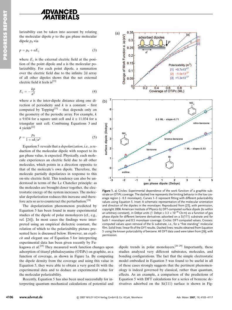
The depolarization phenomenon predicted byEquation 5 has been found in many experimentalstudies of the dipole of polar monolayers (cf., e.g.,ref. [24]). In most cases the findings were inter-preted using an empirical dielectric constant, therelation of which to the polarizability picture pre-sented here is discussed below. However, an expli-cit and elegant use of Equation 5 for interpretingexperimental data has been given recently by Fu-kagawa et al.[25] They measured work function changes uponadsorption of titanyl phthalocyanine (OTiPc) on graphite, as afunction of coverage, as shown in Figure 1a. By computingthe dipole density from the coverage and using this value inEquation 5, they were able to obtain a very good fit with theexperimental data and to deduce an experimental value forthe molecular polarizability.
Recently, Equation 5 has also been used successfully for in-terpreting quantum mechanical calculations of potential and
dipole trends in polar monolayers.[26–29] Importantly, thesestudies analyzed very different substrates, molecules, andbonding configurations. The fact that the simple electrostaticmodel embodied in Equation 5 was found to be useful in allof these cases strongly suggests that the pertinent phenomen-ology is indeed governed by classical, rather than quantum,effects. As an example, a comparison of the predictions ofEquation 5 with DFT calculations for a series of benzene de-rivatives adsorbed on the Si(111) surface is shown in Fig-
PRO
GRES
SREP
ORT
4106 www.advmat.de © 2007 WILEY-VCH Verlag GmbH & Co. KGaA, Weinheim Adv. Mater. 2007, 19, 4103–4117
(a)
-3 -2 -1 0 1 2 3 4 5-1
0
1
2
3
4
5
6
7
gas phase dipole (Debye)
surf
ace
dip
ole
(D
eb
ye) nitro-benzene
bromo-benzene
benzene
aniline
0.5 ML - slope=0.71
1 ML - slope=0.53
NH2
Br
NO2
(b)
Figure 1. a) Circles: Experimental dependence of the work function of a graphite sub-strate on OTiPc coverage. The dashed line represents the limiting behavior in the low cov-erage region (∼ 0.3 monolayer). Curves 1–3 represent fitting with different polarizabilityvalues using Equation 5. Inset: A schematic representation of the molecular orientationand direction of the dipoles in the monolayer. Reproduced from [25], with permission,copyright 2006 American Institute of Physics b) DFT-computed surface dipole (to withinan arbitrary constant), in Debye units (1 Debye ≅ 3.3 × 10⁻³⁰ Cb·m) as a function of gasphase dipole for different benzene derivatives adsorbed on a Si(111) substrate and forboth 1 monolayer and 0.5 monolayer coverage. Circles: DFT-computed values. Crosses:computed values upon removal of the Si substrate, i.e., for a “free standing” molecularfilm. Solid lines: linear fit of the DFTresults. Dashed lines: results obtained from Equation5 using the known polarizability of benzene. All DFTdata used were taken from [26], withpermission.
ure 1b.[26] The agreement between the classical and quantumcalculation is very good and is particularly remarkable, giventhat the lateral distance between the molecules is similar totheir length, i.e., point dipole is not a good approximation forthese molecules. Note, however, that Equation 5 only ad-dresses the dielectric response of individual molecules. Indensely packed molecular layers, collective effects due to in-ter-molecular[30] or molecule-substrate[31] interactions, as wellas significant structural changes,[32] may take place so as tofurther depolarize the monolayer.
Having understood how each molecular dipole is affectedby the presence of other dipoles, the remaining major ques-tion is what electrical potential is generated by an array of(possibly partially depolarized) dipoles. To answer this ques-tion we consider an infinitely periodic array of finite-lengthdipoles, i.e., an infinitely periodic sheet of negative pointcharges at the z = 0 plane, separated from an infinitely peri-odic sheet of positive point charges at the z = d plane. Forsimplicity (and with no loss of generality for the physical con-clusions given below), we assume a rectangular unit cell withrectangle sides of dimensions a and b. The overall spatialcharge distribution, q�x� y� z�, is then given by:
��x� y� z� �
q�∞
k�l��∞d�x � ka� y � lb� z � d� �
�∞
k�l��∞d�x � ka� y � lb� z�
� �
(6)
where q is the proton charge and d(·) is the Dirac delta func-tion. This charge distribution results in a periodic potential.Its form outside the dipolar double layer can be expressed asa Fourier series as an immediate consequence of the expan-sion given by Lennard-Jones and Dent for a planar periodicarray of monopoles.[33] The result is[34]
V�x� y� z� � Vav ��∞
m�n��∞
′ q
ab�����������������������������������m�a�2 � �n�b�2
� ei2p mx
a�ny
b
� �
�e�2p������������������������m�a�2��n�b�2
z�d � e�2p
������������������������m�a�2��n�b�2
z� (7)
where
Vav�z � 0� � Vaz�z � 0� � 4pqdab
�8�
and the prime in the summation indicates exclusion of them=n=0 term. Furthermore, if we let d → 0 while keeping thedipole p=qd constant, we obtain[35]
V�x� y� z� � Vav ��∞
m�n��∞
′ 2ppab
ei2p�mx
a�ny
b�e�2p
������������������������m�a�2��n�b�2
z (9)
The salient point of Equations 7–9 is that for an infinite, pe-riodic 2d array of dipoles, the power-law behavior of an iso-
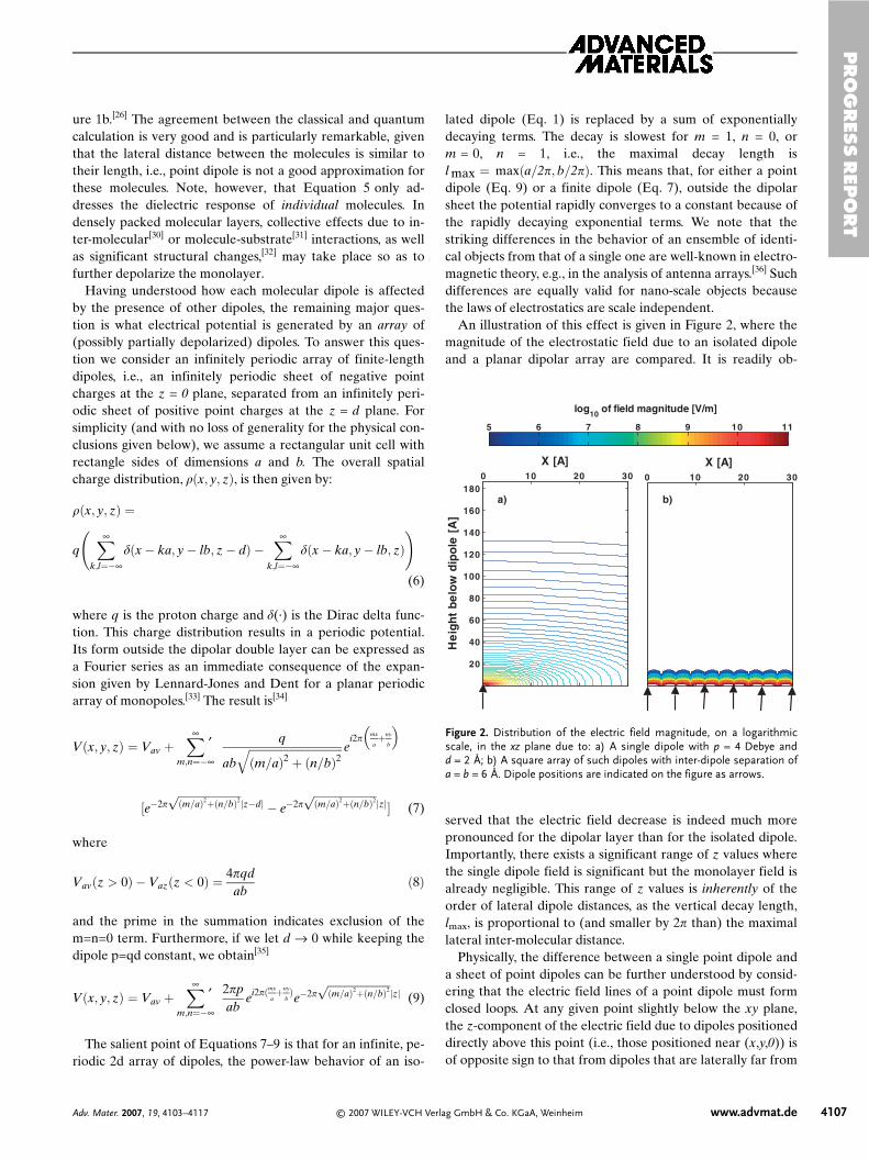
lated dipole (Eq. 1) is replaced by a sum of exponentiallydecaying terms. The decay is slowest for m = 1, n = 0, orm = 0, n = 1, i.e., the maximal decay length isl max � max�a�2p�b�2p�. This means that, for either a pointdipole (Eq. 9) or a finite dipole (Eq. 7), outside the dipolarsheet the potential rapidly converges to a constant because ofthe rapidly decaying exponential terms. We note that thestriking differences in the behavior of an ensemble of identi-cal objects from that of a single one are well-known in electro-magnetic theory, e.g., in the analysis of antenna arrays.[36] Suchdifferences are equally valid for nano-scale objects becausethe laws of electrostatics are scale independent.
An illustration of this effect is given in Figure 2, where themagnitude of the electrostatic field due to an isolated dipoleand a planar dipolar array are compared. It is readily ob-
served that the electric field decrease is indeed much morepronounced for the dipolar layer than for the isolated dipole.Importantly, there exists a significant range of z values wherethe single dipole field is significant but the monolayer field isalready negligible. This range of z values is inherently of theorder of lateral dipole distances, as the vertical decay length,lmax, is proportional to (and smaller by 2p than) the maximallateral inter-molecular distance.
Physically, the difference between a single point dipole anda sheet of point dipoles can be further understood by consid-ering that the electric field lines of a point dipole must formclosed loops. At any given point slightly below the xy plane,the z-component of the electric field due to dipoles positioneddirectly above this point (i.e., those positioned near (x,y,0)) isof opposite sign to that from dipoles that are laterally far from
PRO
GRES
SREP
ORT
Adv. Mater. 2007, 19, 4103–4117 © 2007 WILEY-VCH Verlag GmbH & Co. KGaA, Weinheim www.advmat.de 4107
X [A]0 10 20 30
X [A]H
eig
ht
be
low
dip
ole
[A
]
0 10 20 30
20
40
60
80
100
120
140
160
180
5 6 7 8 9 10 11
log10
of field magnitude [V/m]
a) b)
Figure 2. Distribution of the electric field magnitude, on a logarithmicscale, in the xz plane due to: a) A single dipole with p = 4 Debye andd = 2 Å; b) A square array of such dipoles with inter-dipole separation ofa = b = 6 Å. Dipole positions are indicated on the figure as arrows.
this point. The lateral components of the electric field alsotend to cancel. For example, the y-component of the electricfield due to dipoles positioned at the half-plane (x’,y’ > y,0) isof opposite sign to that due to dipoles positioned at the otherhalf (x’,y’ < y,0). At a point close to the xy plane, the extent ofthe “left-right” and “near-far” cancellations depends on theexact lateral location (x,y) of this point relative to the mesh ofthe molecular dipoles. As one moves away from the dipolarlayer, things smooth out, the electric field becomes increas-ingly negligible, and the potential becomes increasingly closeto a constant.
Again, it is appropriate to ask whether the electrostaticspredictions can really explain first principles quantum me-chanical calculations. First, the basic phenomenology of Fig-ure 2, namely, the induction of significant electric fields in anunderlying substrate from a single polar molecule, but notfrom a molecular monolayer, despite the same local chemistryin both cases (i.e., the same molecule being bound to the samesubstrate in the same way), has been recently confirmed bythe detailed DFT calculations of Deutsch et al.[37] Further-more, we argue that the suppression of significant electricfields in the substrates explains systematically a host of recentmonolayer results that may appear puzzling from a traditionalchemical point of view.
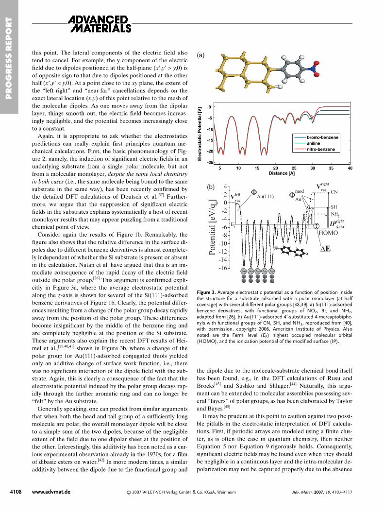
Consider again the results of Figure 1b. Remarkably, thefigure also shows that the relative difference in the surface di-poles due to different benzene derivatives is almost complete-ly independent of whether the Si substrate is present or absentin the calculation. Natan et al. have argued that this is an im-mediate consequence of the rapid decay of the electric fieldoutside the polar group.[26] This argument is confirmed expli-citly in Figure 3a, where the average electrostatic potentialalong the z-axis is shown for several of the Si(111)-adsorbedbenzene derivatives of Figure 1b. Clearly, the potential differ-ences resulting from a change of the polar group decay rapidlyaway from the position of the polar group. These differencesbecome insignificant by the middle of the benzene ring andare completely negligible at the position of the Si substrate.These arguments also explain the recent DFT results of Hei-mel et al.,[29,40,41] shown in Figure 3b, where a change of thepolar group for Au(111)-adsorbed conjugated thiols yieldedonly an additive change of surface work function, i.e., therewas no significant interaction of the dipole field with the sub-strate. Again, this is clearly a consequence of the fact that theelectrostatic potential induced by the polar group decays rap-idly through the farther aromatic ring and can no longer be“felt” by the Au substrate.
Generally speaking, one can predict from similar argumentsthat when both the head and tail group of a sufficiently longmolecule are polar, the overall monolayer dipole will be closeto a simple sum of the two dipoles, because of the negligibleextent of the field due to one dipolar sheet at the position ofthe other. Interestingly, this additivity has been noted as a cur-ious experimental observation already in the 1930s, for a filmof dibasic esters on water.[42] In more modern times, a similaradditivity between the dipole due to the functional group and
the dipole due to the molecule-substrate chemical bond itselfhas been found, e.g., in the DFT calculations of Rusu andBrocks[43] and Sushko and Shluger.[44] Naturally, this argu-ment can be extended to molecular assemblies possessing sev-eral “layers” of polar groups, as has been elaborated by Taylorand Bayes.[45]
It may be prudent at this point to caution against two possi-ble pitfalls in the electrostatic interpretation of DFT calcula-tions. First, if periodic arrays are modeled using a finite clus-ter, as is often the case in quantum chemistry, then neitherEquation 5 nor Equation 9 rigorously holds. Consequently,significant electric fields may be found even when they shouldbe negligible in a continuous layer and the intra-molecular de-polarization may not be captured properly due to the absence
PRO
GRES
SREP
ORT
4108 www.advmat.de © 2007 WILEY-VCH Verlag GmbH & Co. KGaA, Weinheim Adv. Mater. 2007, 19, 4103–4117
5 10 15 20 25 30 35 40-25
-20
-15
-10
-5
0
Distance [A]
Ele
ctro
stat
ic P
ote
ntia
l [V
]
bromo-benzeneanilinenitro-benzene
(a)
-16
-14
-12
-10
-8
-6
-4
-2
0
2
4
Vleft
vac
Vright
vacΦAu(111)
Potential
[eV/qe]
EF
Φmod
Au
IPright
SAM
NH2
SH
CN
Au Au Au AuAu
∆E
HOMO
(b)
Figure 3. Average electrostatic potential as a function of position insidethe structure for a substrate adsorbed with a polar monolayer (at halfcoverage) with several different polar groups [38,39]. a) Si(111)-adsorbedbenzene derivatives, with functional groups of NO2, Br, and NH2,adapted from [26]. b) Au(111)-adsorbed 4′-substituted 4-mercaptobiphe-nyls with functional groups of CN, SH, and NH2, reproduced from [40],with permission, copyright 2006, American Institute of Physics. Alsonoted are the Fermi level (EF) highest occupied molecular orbital(HOMO), and the ionization potential of the modified surface (IP).
of the periodic replicas.[37] The latter observation is consistentwith the observation of Cornil et al., who found that a finitecluster should consist of at least tens of molecules for the de-polarization to reach its monolayer value.[28] If, instead, peri-odic boundary conditions are used, this problem obviouslydoes not arise. However, it is important to note that graphicalrepresentations of potentials that are laterally averaged overthe periodic unit cell, such as those presented in Figure 3,could be misleading. Consider, e.g., the potential given byEquation 9. Because it is, by definition, periodic in x and y,lateral averaging makes all its components except Vav (whichis the m = n = 0 term) vanish at any depth z irrespectively ofactual field penetration! In other words, the xy averaged po-tential outside the dipolar sheet is z-independent. The same istrue if the potential of Equation 9 is screened by a uniform di-electric constant throughout the unit cell. The potentialchanges due to different polar groups, shown in Figure 3, areobserved essentially because the dielectric response is not mi-croscopically uniform. Especially for periodic monolayerswith low molecular coverage, where significant electric fieldscan exist deep within the more uniform bulk, lateral averagingcan grossly under-represent the extent of field penetrationand, similarly, the extent of charge transfer between substrateand molecule.
The preceding arguments highlight intra-monolayer depo-larization and a rapid decay of electric fields outside themonolayer as the hallmarks of monolayer electrostatics. Tak-en together, they allow us to comment on the rationale forand validity of the heuristic Helmholtz equation. This equa-tion relates the potential drop across a polar monolayer, DV,to its gas phase dipole, P0, as:[4,10]
DV � 4pNP0 cos ���
Ae(10)
where A is the surface area, N is the number of molecules, �is the molecular tilt angle relative to the surface normal, and eis an effective dielectric constant of the monolayer (not to beconfused with the bulk dielectric constant of a molecular solidof the same molecules). Sufficiently far away from the polarmonolayer, where all exponential potential terms are negligi-ble, the potential drop across the polar monolayer is given bythe difference of Vav above and below the monolayer andEquation 8 then yields:
DV � 4pp0
ab�1 � ak�a3� (11)
If we identify P0cos(�), the z-component of the moleculardipole, with the point dipole p0; A/N, the “footprint” of a sin-gle molecule, with the area per point dipole, ab; and e, the di-electric constant, with the depolarization factor, 1 + ak/a3,Equations 10 and 11 become identical. We conclude, then,that the uniform density approximation (namely, the parallelplate capacitor model) works because all potential terms dueto non-uniform density components decay exponentially andthat the dielectric constant approximation works because itmimics the intra-molecular depolarization. We also note that
more elaborate models comprising several capacitors for sys-tems with several dipolar layers and also including image ef-fects have been constructed and applied successfully.[44–48]
Using either Equation 10 or Equation 11, we immediatelysee how a molecular layer at the surface contributes a poten-tial drop, DV, that affects the surface work function and/orelectron affinity by eDV. Such effects have indeed been ob-served experimentally for, e.g., Au.[49,50] For semiconductors, aseries of studies by Cahen and coworkers,[4,5] showed that theelectron affinity of many semiconductors, such as CdTe,[51]
CdSe,[52] GaAs,[53] Si,[54] ZnO,[55] and even polycrystallineCuInSe2
[50,51] can be changed systematically by adsorbing setsof benzoic and dicarboxylic acid molecules, with varying di-pole moments (by changing a given substituent in the mole-cules) but identical binding to the semiconductor substrates.In these studies, varying the molecular dipoles was achievedmostly by changing the functional group at the top of themonolayer (cf. Fig. 1b). Similar electron affinity modificationswere observed for, e.g., TiO2,[56] In:SnO2,[57] and SiO2.[58] Gen-erally, a linear relation exists between changes in the electronaffinity and the magnitudes of the gas phase molecular di-poles, as shown in Figure 1b, such that a positive dipole in-creases the semiconductor electron affinity, whereas the useof a negative molecular dipole decreases it.[59] It should benoted, however, that in many of the above experimental stud-ies, straightforward fitting results in an effective dielectricconstant e that is larger than that expected from molecular de-polarization. Possibly, this is because using e as an empiricalfitting parameter allows one to “bury” within it other factors,such as partial coverage, adsorption of foreign molecules (e.g.,water), etc.
In a similar vein, Equations 10 and 11 predict that a interfa-cial dipolar layer can affect the interface dipole and relatedquantities, such as the Schottky barrier height for metal/semi-conductor junctions and the band offset for semiconductorheterojunctions. For example, Campbell et al. have shownthat they can control the Schottky barrier between a metalelectrode and an organic semiconducting film using self-as-sembled monolayers.[60] Several studies have shown the abilityto control the electrical properties of junctions between met-als and inorganic semiconductors by means of adsorbing rela-tively small organic molecules, such as carboxylic acids on thesemiconductor[55,61–63] and cyclic disulfides on the metal sideof the interfaces.[64] Examples of junctions that were studiedinclude Au/GaAs (n- and p-type),[61–63] Au/ZnO,[55] Au/Si(with a thin native oxide),[64] and (oxide free) Hg/Si[65] junc-tions. In most cases, systematic changes in charge transportbehavior across the molecularly modified junctions were in-deed observed.
Importantly, for monolayers “sandwiched” between a metaland a semiconductor the net interfacial dipole direction canbe a strong function of the molecular bond to the substrateand/or the nature and method of deposition of the contactmetal.[62] In fact, a comparison of different contacting modeshas shown that an intimate contact (i.e., < 1–2 Å proximity)between the molecules’ exposed substituents and the (top)
PRO
GRES
SREP
ORT
Adv. Mater. 2007, 19, 4103–4117 © 2007 WILEY-VCH Verlag GmbH & Co. KGaA, Weinheim www.advmat.de 4109

metal contact completely inverted the molecular dipole effecton the electrical characteristics of the resulting devices. Thisbehavior was explained by effective dipole inversion due tometal-molecule polarization and partial charge redistributionbetween metal and molecules[62] (cf. also refs. [66] and [67]).A similar effect, suggesting dipole inversion, was found forAu contacts evaporated indirectly, on a cooled substrate, on an-GaAs substrate bearing a molecular monolayer.[68,69] If Pdwas used instead of Au, no such inversion was observed.[68,70]
This striking difference was attributed to the difference ingrowth mechanisms of the Pd and Au films, viz., two dimen-sional and three dimensional growth, respectively, that leadsto differences in the interaction of the metal with the mole-cules.[69]
Finally, it is well-known that a dipole at a semiconductor-in-sulator interface of a metal/insulator/semiconductor junctionwill change the threshold voltage of a field effect transistorbased on this structure. This means that this quantity, too, canbe controlled by polar organic layers. This has been elegantlydemonstrated by Kobayashi et al.,[71] who showed that theycould control the surface carrier density in an organic thinfilm transistor using organosilane self-assembled monolayerssandwiched between the SiO2 insulator and the active organicfilm.
3. Electrostatics of Non-ideal Polar Monolayers
Obviously, the perfectly ordered, infinitely periodic molecu-lar monolayer studied in the previous section is an idealiza-tion that is rarely encountered in practice. However, as shownabove, this does not mean that it cannot capture correctlysome of the salient features of realistic monolayers. In thissection, we discuss various non-ideal scenarios, with an em-phasis on identifying monolayer properties and ensuing de-vice behavior where significant qualitative discrepancies be-tween ideal and real monolayers are expected.
Because organic monolayers often form domains,[72] westart by considering the electrostatics of an ordered array ofpoint dipoles of finite size. To understand how the electricfield distribution differs from that of an infinite monolayer,we compute the electric field distribution below such an arrayby numerically superposing the field of each dipole in the ar-ray, as given by Equation 1. For simplicity, we again neglectdepolarization effects. Note, however, that the depolarizationwithin a finite domain is not uniform because the electricfields at the center and at the edge of the domain are not thesame, as elaborated below. This can make a quantitative dif-ference, but can be neglected to first order for a discussion ofqualitative features.[73]
Several different views of an instructive example – rectan-gular finite domains of various sizes, each consisting of thesame dipoles as studied in Figure 2 – are given in Figure 4.
The electric field distributions due to finite dipolar domainswith dimensions of 60 × 60 Å2, 120 × 120 Å2, and 240 ×240 Å2 are given in Figure 4a and b, respectively, for planes
lying 10 Å and 100 Å below the dipolar layer. At 10 Å belowthe dipolar layer, there is a pronounced edge effect, similar tothat of a classical plate capacitor: The field is stronger at theedge and is by-and-large independent of the domain size. Thefield decays towards the center of the domain. At the center,the electric field value is smaller the larger the domain is. At100 Å below the dipolar layer, a different picture emerges:the field is more uniform, it increases with increasing domainsize, and it shows larger values below the center than belowthe edges. More insight into these profound differences canbe gained from inspecting Figure 4c, which shows the distribu-tion of the magnitude of the total electric field at the domaincenter and the (center of the) domain edge for three differentfinite dipolar domains, with lateral dimensions of 84 × 84 Å2,900 × 900 Å2, and 9000 × 9000 Å2. At one extreme, close tothe dipolar layer the electric field at the domain center (solidline) does not differ appreciably from the exponentially de-caying field of an infinite dipolar layer (dotted line). This isbecause in this “near field” regime, the termination of the do-main is “too far” to have an appreciable effect. Naturally, thelarger the domain is the larger the extent of the “near field”regime is (one can say that for an infinite layer, the electricfield is always at the “near field” regime). At the other ex-treme, at large distances the electric field at the center of thedomain attains a “far field” asymptotic behavior (dashedlines), where the field scales as 1/r3 and the domain can essen-tially be thought of as a single dipole at the origin, whose mag-nitude is the simple sum of all the individual dipoles. Natu-rally, the larger the domain is, the further away the onset ofthe “far field” regime appears.
As expected, Figure 4c reveals a large intermediate rangewhere neither limit applies. On the one hand, the cancellationof the contributions of different dipoles, which is at the heartof the exponential decay for an infinite monolayer, is far fromcomplete. On the other hand, the variation in distances to in-dividual dipoles is too large to view them as one large,“merged” point dipole. The figure also reveals that the elec-tric field at the center of the domain is nearly constant – andnot necessarily negligible – over most of the intermediaterange. Because the cross-over from the intermediate to the“far field” regime takes place when the solid angle at whichthe domain is viewed is at some critical angle, the “far field”limit for any domain, with a length D on each side, is attainedat a height (z) with a fixed z/D ratio. At that point, the magni-tude of the electric field is of the order of p/z3, where p, theoverall dipole, scales as ∼ D2. Thus, at the cross-over pointand throughout the “nearly constant” regime, the electricfield scales as 1/D. In other words, the “plateau” in Figure 4cis inversely proportional to the domain size.
Importantly, the electric field at the edge of the domain(dash-dotted lines in Fig. 4c) is significantly larger than thefield at the center upon departure from the “near field” re-gime. It decreases approximately as ∼ 1/r, eventually becom-ing smaller than the field at the center before they both mergeat the “far field” limit. However, the direction of the electricfield at the center and at the edge is not the same. Figure 4d
PRO
GRES
SREP
ORT
4110 www.advmat.de © 2007 WILEY-VCH Verlag GmbH & Co. KGaA, Weinheim Adv. Mater. 2007, 19, 4103–4117

PRO
GRES
SREP
ORT
Adv. Mater. 2007, 19, 4103–4117 © 2007 WILEY-VCH Verlag GmbH & Co. KGaA, Weinheim www.advmat.de 4111
10100
10101
10102
10103
10104
10103
10104
10105
10106
10107
10108
10109
10101010
Heigightht b belolow w domainin [ [A]
Fie
ld M
d M
ag
ng
nitit
ud
eu
de
[V
/m]
8484Ax8484A
900A00Ax900A900A
9000A000Ax9009000A0A
(a) (b)
(c) (d)
X [A]
log
10 Z
[A
]
-600 -400 -200 0 200 400 6000
0.5
1
1.5
2
2.5
3
6 7 8 9 10 11
log10
of field magnitude [V/m](e)
Figure 4. Several different perspectives on the electric field distribution due to a finite square arrays of p = 4 Debye, d = 2 Å dipoles with inter-dipoleseparation of a = b = 6 Å. a) Distribution of the magnitude of the total electric field in the xy plane (with the domain center at x = y = 0 ), at a distanceof 10 Å (“near field”) below dipolar arrays with overall lateral dimensions of 60 × 60 Å2, 120 × 120 Å2, and 240 × 240 Å2. b) same as (a), but at a dis-tance of 100 Å below the layer (“far field”). c) Magnitude of the total electric field as a function of distance below the domain, z, for dipolar arrays withoverall lateral dimensions of 84 × 84 Å2, 900 × 900 Å2, and 9000 × 9000 Å2, at the domain center (solid lines) and below the center of its edge (dash-dotted lines). Note that all dash-dotted lines converge for small enough z values. Also shown are the “near field” (dotted line) and “far field” (dashedlines) asymptotic curves. d) Contour plot of the distribution of the z-component of the electric field at the xz plane, for a 600 × 600 Å2 finite array.e) Same as (d), for the x-component of the electric field.

and e provide contour plots for the z-component and thex-component, respectively, for a 600 × 600 Å2 domain. Fromsymmetry argument, at the center of the domain the fieldmust be in the z direction. But as one moves towards the edge,the x-component of the electric field becomes larger andeventually dominates. Near the edge of the domain, then, theabsence of “left-right” cancellation of dipoles is more pro-nounced than the absence of “near-far” cancellation. This isreasonable, because at the edge all dipoles are either “left” or“right”, but some are still “near” and some “far”.
The above-elaborated behavior of the rectangular domainis qualitatively typical to domains whose extent in both lateraldirections is similar. Consider, however, a rectangular domainof lateral dimensions a × b, such that a >> b, the most extremecase of which is a one-dimensional finite dipolar line. FromGauss’ law, the electric field outside a charged wire (as op-posed to plate) with a uniform one-dimensional charge den-sity, k, is Er � k�2pr. Taking two such wires, separated by adistance d, we obtain, for d → 0, that Ez straight above thetwo wires is given by p�2pr2, where p is the one-dimensionaldipole density. This is fundamentally different than the pre-vious case (but note that numerical calculations show thatedge behavior is similar in the two systems).
It is also very important to consider a different kind of do-mains, where molecules are absent from a region of adsorp-tion sites, a process which often occurs naturally in mono-layers.[72] From an electrostatic perspective, the superpositionprinciple tells us that electric field due to an otherwise idealdipolar monolayer with a “pinhole” is simply the differencebetween the electric field of the perfect monolayer and theelectric field of the “missing domain”. This is illustrated inFigure 5 for the simplest “missing domain” possible – a singlemissing dipole. Because the field of the perfect monolayer de-cays rapidly, at vertical distances of the order of the lateraldistance between dipoles the electric field is very similar tothat of a single dipole in the opposite direction. This isstraightforward from the electrostatics point of view, but hasinteresting chemical consequences: Assuming a fixed bindinggroup, the electric field “felt” by the substrate due to a finite-domain of molecules with a strongly electron-donating groupand that due to a hole-possessing monolayer with a stronglyelectron-withdrawing group, are essentially the same if the“hole” and the domain are of the same dimensions. This is soeven though the modification of the work function are of op-posite sign in the two cases.
Interestingly, finite-domain electrostatic effects of the typeshown in Figures 4 or 5 will not be captured by DFT calcula-tions of either a single (or a few) molecules on a cluster or ofan ideal periodic monolayer. If we wish to include such effectswithin a DFT calculation without explicitly computing theelectronic structure of at least hundreds or possibly thousandsof molecules, the proper electrostatic regime will have to beenforced by adding additional terms to the Hamiltonian. Tothe best of our knowledge, this has not been done.
Turning our attention to experiment, one striking examplewhere the experimentally observed behavior of an electronic
device cannot be reconciled even qualitatively with the prop-erties of ideal monolayers, but are well explained by consider-ing non-ideal monolayers, is found in the study of metal-semi-conductor junctions possessing a molecularly-modifiedinterface.[19,63,74,75] Here, we examine the Au/(CH3-terminateddicarboxylic acid)/n-GaAs junction, where Au is gently evap-orated on the n-GaAs substrate bearing molecular monolayer,as a prototypical case.[76] For this system various measure-ments, e.g., quantitative x-ray photoelectron spectroscopy(XPS) and Fourier transform infrared spectroscopy (FTIR)confirmed that the (top) contact-free molecular monolayer isdiscontinuous. That this is also the case also with an appliedtop contact was confirmed by ballistic electron emission mi-croscopy (BEEM) as shown in Figure 6.[75]
A comparison of conventional STM topography of the Au/n-GaAs junction, with or without the interfacial molecularmonolayer (Fig. 6a and c) reveals a similar Au grain structure.The simultaneously-measured BEEM current map, however,reveals relatively small (mostly < 3 pA) spatial variations inthe current amplitude that are strongly correlated with thepolycrystalline grain structure of the Au film of the bare Au/n-GaAs sample (Fig. 6b), but not with that of the molecularlymodified one (Fig. 6d). In the latter case, the BEEM currentis extremely small over most of the image area, except at iso-lated bright patches that are ∼ 20 nm across in size. SchottkyBarrier heights (SBH), extracted at various lateral positionsin both samples, are consistent with these current-map-basedobservations. Analysis of BEEM current-voltage curves atvarious lateral locations shows that for the bare Au/n-GaAssample the SBH is quite uniform, with a mean of ∼ 0.92 eVand a standard deviation of ∼0.02 eV. For the monolayer-in-serted Au/n-GaAs sample, the local SBHs measured at 10 dif-ferent pinholes were found to have a mean value of ∼ 0.95 eVwith a standard deviation of ∼ 0.03 eV. These values were
PRO
GRES
SREP
ORT
4112 www.advmat.de © 2007 WILEY-VCH Verlag GmbH & Co. KGaA, Weinheim Adv. Mater. 2007, 19, 4103–4117
X [A]
He
igh
t b
elo
w d
ipo
le [
A]
0 50 100 150
20
40
60
80
100
120
140
160
180
X [A]
0 50 100 150
5 6 7 8 9 10 11
log10
of field magnitude [V/m]
a) b)
Figure 5. Distribution of the electric field magnitude, on a logarithmicscale, in the xz plane due to: a) A single dipole with p = 4 Debye andd = 2 Å; and b) A square array of such dipoles with inter-dipole separa-tion of a = b = 6 Å, with the dipole at x = y = 0 missing.

largely in agreement with those previously estimated for simi-lar samples using macroscopic temperature-resolved current-voltage, capacitance-voltage, and internal photoemissionspectroscopy measurements.[19] Because the molecule studiedis expected to increase the Schottky barrier height (SBH), aswell as to pose an additional tunneling barrier to current, theBEEM results strongly suggest that (at least for the tip biasused) the current flowing directly through the molecularmonolayer is negligible. Instead, significant current flows onlythrough ∼ 20 nm size pinholes in the monolayer, where a di-rect Au/n-GaAs contact is established.
The main reason for the drastic reduction in junction cur-rent over the interface areas with the molecular layer presentis likely the low transmission coefficient of carriers acrossmolecules.[77] Because most current across the Au/(dicar-boxylic acid)/n-GaAs interface has passed through small areasdevoid of molecules, it may seem that the dipole moment ofthe molecular layer is irrelevant for current transport. How-ever, the experimental data show that the effective SBH forpinhole conduction has been influenced by the dipole of themolecular layer, possibly due to the edge effects elaborated inFigure 4. Effectively, the conduction path through the (semi-conductor below the) pinhole is “gated” by fringing electricfield from the surrounding molecular layer.[78,79] If the polarityof the molecular dipole is such that it increases the SBH, as inFigure 6, the effect of the molecular layer is equivalent to a“reverse gate bias” applied to the pinhole conduction path.This makes the effective SBH for the pinhole larger, in agree-ment with experiment. Clearly, the effect can become negligi-ble for sufficiently large pinholes. Conversely, for smallenough pinholes dipoles of the molecular layer can effectively“pinch-off”[80] the current through the pinhole.[81]
We point out that the pinch-off of current through low-re-sistance patches of a metal-semiconductor junction is not lim-
ited to those with partial molecular dipole layers inserted atthe interface. It is known that the current transport acrossbare Schottky barriers, which are fabricated (intentionally orunintentionally) with spatially inhomogeneous barrier height,can also be significantly influenced by the potential “pinch-off” effect.[78] The conduction paths in front of low-barrier-height patches can exhibit band-bending due to the presenceof high-barrier-height region in close proximity. This electro-static phenomenon, which is of the same nature as that pres-ently discussed for molecular dipole layers, is well understoodexperimentally and theoretically for inhomogeneous Schottkybarriers, and has been discussed in ref. [78]. Interestingly, themodeling of the band-bending at inhomogeneous, but bare,Schottky barriers was most conveniently carried out by as-suming the presence of an inhomogeneous dipole layer at theinterface, reminiscent of the morphology of partial moleculardipole layer in our discussion. That simple model then led toanalytic expressions for the inhomogeneous Schottky barrierswhich were found to be in agreement with experimental dataand computer simulation results.
A different type of electronic device that is dominated byelectrostatic effects in dipolar layers is the FET-like structuresthat are used for sensing chemical processes. Such devices aregenerally known as CHEMFETs. There are many differentvarieties of CHEMFETS (see, e.g., refs. [82–84] for over-views), most of which, however, are loosely based on the sameprinciple: The presence of molecules or ions influences thepotential of the conducting FET channel either by directly in-fluencing the gate potential (e.g., for a catalytically activemetal gate) or by changing the potential distribution betweena “reference electrode gate” and the semiconductor. As is of-ten the case in electronic devices (e.g., with the concept ofdoping), extremely small chemical perturbations can havelarge electrical consequences. This means that properly de-signed CHEMFETs are sensitive to, and can be used to de-tect, minute concentrations of chemicals. In CHEMFETs witha reference gate, even an ideal polar layer can induce a signifi-cant field in the channel.[85,86] This field ensues because theoverall potential difference between the ground and the refer-ence electrode must remain the same with or without the po-lar layer, i.e., fields external to the dipole layer must be in-duced so as compensate for the potential drop on it[10] (thesame reasoning applies to the results of Kobayashi et al.,[71]
discussed at the end of the previous section).Chemical sensing with FETs having no reference electrode,
shown schematically in Figure 7, relies on a somewhat differ-ent mechanism. Such devices have generally been referred toas molecularly controlled semiconductor resistors (MOC-SERs).[17] In MOCSERs, the traditional gating electrode iseither present at the back, with a molecular layer adsorbed di-rectly on the semiconductor (Fig. 7a),[18] or is replaced alto-gether by a molecular layer adsorbed on a (typically ultra-thin) dielectric (Fig. 7b).[16] In either configuration, bindingmolecules from the gas or liquid phase to the “chemical sens-ing molecules” changes the potential in the conducting chan-nel. Consequently, the current between source and drain is
PRO
GRES
SREP
ORT
Adv. Mater. 2007, 19, 4103–4117 © 2007 WILEY-VCH Verlag GmbH & Co. KGaA, Weinheim www.advmat.de 4113
Figure 6. a) STM and b) simultaneous BEEM image (measured at anSTM tip bias of 1.2 V) of a “bare” Au/n-GaAs sample, i.e., without a mo-lecular monolayer. Color scales are 3.4 nm and 3 pA, respectively. c) STMand d) simultaneous BEEM image (measured at an STM tip bias of1.38 V) of a Au/(CH3-terminated dicarboxylic acid)/n-GaAs sample. Col-or scales are 3.6 nm and 1 pA, respectively. Numbers in Gray are localSchottky barrier heights and the number in red is the applied bias. Repro-duced from [75], with permission).

modified and the device serves as a sensor. Such devices canhave high chemical sensitivity. For example, a GaAs-basedMOCSER with a monolayer of suitable porphyrins was usedsuccessfully to detect ∼ppb concentrations of NO in bothphysiological solution,[16,86] and in air.[87] A high-sensitivityMOCSER based on GaN/AlGaN has been similarly used forpolar liquid sensing.[88]
The pertinent question for our discussion is the mechanismthrough which the potential in the conductive channel is mod-ified by adsorption of a polar layer on a MOCSER. In either aCHEMFET or a MOCSER (i.e., with or without a referenceelectrode, respectively), if charged species are adsorbed, or ifthe surface is effectively charged upon adsorption, then po-tential modifications at the channel necessarily take place,from an electrostatic point of view. However, the homoge-neous adsorption of a layer of polar yet neutral molecules onthe device structures of Figure 7 has no first order effect onthe electrostatics of the conduction channels, based on the ar-guments of Section 2. Therefore, one would not expect the ad-sorption of an ideal polar monolayer to be detectable in struc-tures without reference gates. Nevertheless, the detection ofthe changes in the dipole moment of a functional group byMOCSERs has been observed experimentally. Clear-cut evi-dence for this was recently provided by He et al.[18] Using adevice structure as in Figure 7a, they showed a distinct corre-lation between the threshold voltage of the FET and the po-larity of the functional group for molecules of the type shownin Figure 3a. For device structures as shown in Figure 7b, Ru-dich et al.[89] found that adsorption of a small fraction(∼ 10 %) of either H2O or O2 on a MOCSER, with a channelcovered by a monolayer of alkyl chains, yielded very large sig-
nals, but in opposite directions. This has also been interpretedin terms of opposite directions of the dipole moment inducedin the monolayer upon adsorption of the detected species.[17]
Likewise, the above-mentioned work on NO detection[16,86]
has been discussed in terms of induced dipoles, rather than ad-sorption of charged species.
One plausible explanation of the observed results seems tobe that the residual fields outside the (uniform) dipole layerare still sufficient to induce a very small degree of chargetransfer between substrate and organic layer. The net chargedue to this transfer could then modulate the field in the chan-nel.[17] He et al. estimated the changes in charge transferbetween different benzene derivatives to be of the order of∼ 10–3 e.[18] Similar numbers were indeed found in the DFTcalculations of Natan et al.[27] Although this is a minute chargefrom a chemical point of view, it is large in electrical termsand would seem to be amenable to detection. However, thefields associated with such charge transfer are still those of adipole rather than of a monopole. Thus, the observed currentmodulation in conduction channels whose depth below thesurface is large compared to the inter-molecular spacing is stillleft unaccounted for.
It seems that in these devices issues of practical, non-idealmonolayers have to be considered. One such issue that wehave not considered so far is that of surface states, which natu-rally arise at any surface which is not perfectly passivated(see, e.g., ref. [10] for a detailed discussion). Such states pro-vide a monopolar surface charge density. Cohen et al. haveshown experimentally that, for a variety of semiconductors,adsorption of molecules possessing the same binding groupbut different polar groups may significantly change the sur-face band bending by modifying the surface state distribu-tion.[14] This was interpreted in terms of frontier orbital inter-action[90] between the surface states of the substrate and thelowest unoccupied molecular orbital of the molecule. Suchmodification of surface states could well cause the above-mentioned relatively minute change in monopolar charge re-quired to drive the MOCSER. Even if surface states are notan issue, one should recall that the entire MOCSER devicehas a finite lateral extent and is therefore a finite domain inthe sense discussed above. Furthermore, even if the “chemicalsensing monolayer” is ideal, the picture of an ideal layer ofanalyte molecules adsorbing on the surface like a spread-outblanket descending on a mattress is clearly unrealistic. Thus,in addition to the inherent non-ideality of the chemical sens-ing monolayer, there will be additional non-ideality inducedby partial adsorption, generating smaller polar domains insidethe active area of the device. In either case, Figure 4 then im-mediately leads to non-negligible fields that can appear at ap-preciable depths inside the MOCSER structures and ergogenerate meaningful signals.
To the best of our knowledge, this reasoning has not beenexplored quantitatively yet and we are not aware of experi-ments where the MOCSER signal was studied as a function ofa well-controlled device size, degree and pattern of surfacecoverage, and channel depth for a well-passivated surface. In-
PRO
GRES
SREP
ORT
4114 www.advmat.de © 2007 WILEY-VCH Verlag GmbH & Co. KGaA, Weinheim Adv. Mater. 2007, 19, 4103–4117
Gate
Dielectric Layer
DrainSource
Semi-conductive Channel
Gate
Dielectric Layer
DrainSource
Semi-conductive Channel
Analyte
Molecule
Chemical Sensing
Molecules(a)
Semiconductor
Dielectric Layer
DrainSource
Semiconductor
Dielectric Layer
DrainSource
Chemical Sensing
Molecules
Analyte
Molecule(b)
Figure 7. Schematic representation of MOCSER structures used forchemical sensing without a reference electrode: a) the molecular layer isadsorbed directly on the semiconductor and the gating is done from theback. b) the FET gate is replaced by a molecular layer adsorbed on the(thin) dielectric.

terestingly, Wu et al.[86] found that the MOCSER signal with amixed hemin/benzoic acid layer gave a much stronger re-sponse signal to NO than a device with a pure hemin mono-layer, even though NO is only adsorbed on the hemin mole-cules. Possibly, this is simply because adding the carboxylatespacer enhances the NO binding rate to the hemin (a fact alsoevident from the shorter time constant found with the spacer).However, atomic force microscopy (AFM) images on mica re-vealed a clear domain pattern of adsorption with the carbox-ylate spacer and this may also serve to explain the enhancedsignal.
In the context of both the molecularly modified Schottky-diodes and the MOCSER devices, another possible degree offreedom in device design is that of deliberate patterning,namely the engineering of domains possessing polar mole-cules and domains devoid of them, e.g., by modern lithogra-phy techniques. The Fourier spectrum of the charge distribu-tion of such a pattern would be a convolution between theFourier spectrum of the pattern function and the Fourier spec-trum of the ideal monolayer.[91] This will necessarily lead tolong-range lateral Fourier components that, in analogy toEquation 9, would lead to large vertical decay lengths. Natu-rally, for MOCSER applications one would need to explorethe effect of significant lateral variations in channel potentialon the device performance.[78,79]
Before concluding this section, we note that recently therehas been much experimental interest in molecular sensorsbased on molecule adsorption on nano-wires (e.g., refs. [92–95]) or (semiconducting) nano-tubes (e.g., refs. [96–98]). In 1dsystems, as in the 2d systems studied above, the behavior of anideal molecular layer can be approximated to zero order by acapacitor, except that here it is a parallel cylinder rather thana parallel plate capacitor. Still, there would be no electric fieldoutside the “capacitor”, i.e., inside the nano-wire. Arrange-ments of point dipoles with cylindrical symmetry can be treat-ed, similar to procedures given in Equations 7–9, in cylindricalcoordinates. This leads to a Fourier–Bessel expansion for thepotential.[21] The sum of decaying exponentials is replaced bya sum of decaying modified Bessel functions, where again thedecay is of the order of the inter-molecular distance. The lessdense coverage along the cylinder diameter is, the larger thedecay length of the electric field into the nano-wire is. Thecrucial difference from the 2d cases we analyzed so far, how-ever, is that the active cross-section of the device is inherentlysmaller. This is obviously true for a nano-tube, where onlyone, or a few, substrate “monolayers” exist. But even in anano-wire, the portion of the “substrate” influenced by theelectric fields can be much greater than in a 2d device.[99]
4. Concluding Remarks
In this article, we have analyzed the effect of both ideal andnon-ideal polar monolayers on electronic devices entirely interms of classical electrostatics. We have shown that very sim-ple considerations can in fact be highly predictive for a wide
range of seemingly different phenomena. Most importantly,we have shown that the analysis of infinitely periodic polarmonolayers explains modifications of surface and interfacepotentials, whereas the analysis of finite-domain monolayersreadily explains experimentally observed field effects, unex-pected from ideal monolayers. Note, however, that we madeno attempt to incorporate either thermodynamic or kineticconsiderations that would, predict, e.g., driving forces for do-main formation. Instead, we focused on the electric conse-quences of an already-formed ideal or non-ideal monolayer.
It may appear surprising that classical theory is sufficient todescribe the dominant phenomena in what is obviously a com-plicated quantum system. This is rationalized by invokingKohn’s “near-sightedness principle” of quantum me-chanics.[100] According to this principle, perturbation of theexternal potential at a distant region from a given locationgenerally has a small effect on any static property of a many-particle system at that location. This means that outside theimmediate vicinity of the dipole, “near-sightedness” prevailsand detailed quantum mechanical considerations are no long-er necessary.
Specifically, long-range electric fields are an exception to the“near-sightedness principle”.[100] This fact is cardinal to theanalysis performed in this paper. First, it is the fundamentalreason why away from the monolayer it is sufficient to consid-er electric fields, the treatment of which is handled very wellby classical theory. Second, it is responsible for the breakdownof the assumption tacitly made in many chemical analyses, i.e.,that all system properties are controlled by the local chemicalenvironment. This is precisely why we witness such strong“cooperative field effects”,[17] i.e., field effects that are deter-mined by the entire ensemble of polar molecules, rather thansolely by the properties of the individual molecules.
Quantum mechanics is, however, crucial for understandingproperties determined by local interactions, i.e., the gas phasedipole of the polar molecule and its possible modificationupon bonding to a substrate and/or an overlayer. For example,the dipole inversion upon deposition of a top metal contact,[62]
discussed in Section 2, is certainly outside the scope of classi-cal electrostatics. Moreover, sufficiently strong “cooperativefield effects” can, in turn, affect local properties to the extentthat quantum mechanics is needed again. For example, forhighly polar molecules, it is in fact not at all obvious that amolecular monolayer would form, because of the energy pen-alty associated with packing a polar monolayer due to the re-pulsive dipole-dipole interactions.[24] And even if such a layerdoes form, the strong electric fields within it may cause a com-plete rearrangement of the molecular electronic structure bychanging the energy landscape to the extent that the gas phaseenergy minimum is no longer relevant.[101] In such cases, a de-tailed treatment of all energy components, including all mole-cule-substrate and molecule-molecule interactions, in the newground-state, is necessary before application of the electro-static theory presented in this theory is meaningful.
In conclusion, we hope to have elucidated the interplay be-tween local chemical structure and global geometric consid-
PRO
GRES
SREP
ORT
Adv. Mater. 2007, 19, 4103–4117 © 2007 WILEY-VCH Verlag GmbH & Co. KGaA, Weinheim www.advmat.de 4115

erations, as mediated by long-range electric fields. We alsohope to have explained how this interplay manifests itself inpractical electronic devices and to have provided tools for theanalysis and considerations for the design of molecular mono-layers for controlling such devices.
Received: July 11, 2007Revised: August 29, 2007
–[1] Molecular Electronics: Science and Technology (Eds: A. Aviram,
M. Ratner), New York Academy of Sciences, New York 1999.[2] J. R. Heath, M. A. Ratner, Physics Today 2003, 56, 43.[3] Introducing Molecular Electronics (Eds: G. Cuniberti, G. Fagas,
K. Richter), Springer, Berlin 2005.[4] G. Ashkenasy, D. Cahen, R. Cohen, A. Shanzer, A. Vilan, Acc.
Chem. Res. 2002, 35, 121.[5] A. Vilan, D. Cahen, Trends Biotechnol. 2002, 20, 22.[6] B. O’Reagan, M. Grätzel, Nature 1991, 353, 737.[7] J. J. Wei, C. Schafmeister, G. Bird, A. Paul, R. Naaman, D. H. Wal-
deck, J. Phys. Chem. B 2006, 110, 1301.[8] a) Z. Vager, R. Naaman, Chem. Phys. 2002, 281, 305. b) I. Carmeli,
V. Skakalova, R. Naaman, Z. Vager, Angew. Chem. Int. Ed. 2002, 41,761.
[9] P. Crespo, R. Litrán, T. C. Rojas, M. Multigner, J. M. de la Fuente,J. C. Sánchez-López, M. A. García, A. Hernando, S. Penadés,A. Fernández, Phys. Rev. Lett. 2004, 93, 087204.
[10] L. Kronik, Y. Shapira, Surf. Sci. Rep. 1999, 37, 1, Sections 2.1.4, 2.1.5,and 5.2.
[11] B. D. Campbell, H. E. Farnsworth, Surf. Sci. 1968, 10, 197.[12] A. Franciosi, C. G. Van de Walle, Surf. Sci. Rep. 1996, 25, 1.[13] a) T. dell’Orto, J. Almeida, C. Coluzza, A. Baldereschi, G. Margari-
tondo, M. Cantile, S. Yildirim, L. Sorba, A. Franciosi, Appl. Phys.Lett. 1994, 64, 2111. b) M. Marsi, R. Houdre, A. Rudra, M. Ilegems,F. Gozzo, C. Coluzza, G. Margaritondo, Phys. Rev. B 1993, 47, 6455.
[14] a) R. Cohen, L. Kronik, A. Shanzer, D. Cahen, A. Liu, Y. Rosen-waks, J. K. Lorenz, A. B. Ellis, J. Am. Chem. Soc. 1999, 121, 10545.b) R. Cohen, L. Kronik, A. Vilan, A. Shanzer, Y. Rosenwaks, D. Ca-hen, Adv. Mater. 2000, 12, 33.
[15] I. Higuchi, T. Ree, H. Eyring, J. Am. Chem. Soc. 1955, 77, 4969.[16] D. G. Wu, G. Ashkenasy, D. Shvarts, R. V. Ussyshkin, R. Naaman,
A. Shanzer, D. Cahen, Angew. Chem. Int. Ed. 2000, 39, 4496.[17] D. Cahen, R. Naaman, Z. Vager, Adv. Funct. Mater. 2005, 15, 1571.[18] T. He, J. He, M. Lu, B. Chen, H. Pang, W. F. Reus, W. M. Nolte, D. P.
Nackashi, P. D. Franzon, J. M. Tour, J. Am. Chem. Soc. 2006, 128,14537.
[19] H. Haick, M. Ambrico, T. Ligonzo, R. T. Tung, D. Cahen, J. Am.Chem. Soc. 2006, 128, 6854.
[20] See, e.g., a) G. P. Srivastava, Theoretical Modeling of SemiconductorSurfaces: Microscopic Studies of Electrons and Phonons, World Sci-entific, Singapore 1999. b) G. P. Srivastava, Rep. Prog. Phys. 1997,60, 561.
[21] See, e.g., J. D. Jackson, Classical Electrodynamics, 2nd ed., Wiley,New York 1975.
[22] J. R. MacDonald, C. A. Barlow, Jr., J. Chem. Phys. 1963, 39, 412.[23] J. Topping, Proc. R. Soc. London Ser. A 1927, 114, 67.[24] a) O. Gershevitz, C. N. Sukenik, J. Ghabboun, D. Cahen, J. Am.
Chem. Soc. 2003, 125, 4730. b) O. Gershewitz, M. Grinstein, C. N.Sukenik, K. Regev, J. Ghabboun, D. Cahen, J. Phys. Chem. B 2004,108, 664.
[25] H. Fukagawa, H. Yamane, S. Kera, K. K. Okudaira, N. Ueno, Phys.Rev. B 2006, 73, 041302.
[26] A. Natan, Y. Zidon, Y. Shapira, L. Kronik, Phys. Rev. B 2006, 73,193310.
[27] V. De Renzi, R. Rousseau, D. Marchetto, R. Biagi, S. Scandolo,U. del Pennino, Phys. Rev. Lett. 2005, 95, 046804.
[28] D. Cornil, Y. Olivier, V. Geskin, J. Cornil, Adv. Funct. Mater. 2007,17, 1143.
[29] G. Heimel, L. Romaner, E. Zojer, J.-L. Brédas, Nano Lett. 2007, 7,932.
[30] V. Perebeinos, M. Newton, Chem. Phys. 2005, 319, 159.[31] L. Segev, A. Salomon, A. Natan, D. Cahen, L. Kronik, F. Amy, C. K.
Chan, A. Kahn, Phys. Rev. B 2006, 74, 165323.[32] M. L. Sushko, A. L. Shluger, J. Phys. Chem. B 2007, 111, 4019.[33] J. E. Lennard-Jones, M. Dent, Trans. Faraday Soc. 1928, 24, 92.[34] In Equations 7 and 9 the potential is expressed using complex nota-
tion for convenience. However, the result is necessarily real becausethe contributions from the m,n and –m,–n terms in the summationare so that the imaginary part is zero.
[35] Obtaining the limit involves a step where the term�����������������������������������m�a�2 � �n�b�2
�d
is taken to zero when d tends to zero. This is not a valid limit for anarbitrary m,n pair as these Fourier indices can be arbitrarily large.However, because of the exponential decay in z, one can always findan m,n pair of values such that all potential terms above it are arbi-trarily small. Therefore, the limit needs to be taken in practice onlyfor finite values of m,n and is therefore correct.
[36] See, e.g., F. J. Zucker, Robert E. Collin, Antenna Theory, McGraw-Hill, New York 1969.
[37] D. Deutsch, A. Natan, Y. Shapira, L. Kronik, J. Am. Chem. Soc.2007, 129, 2989.
[38] Note that details of the electrostatic potential near the nuclei differin parts (a) and (b) of Figure 3. This is merely a consequence ofwhether the electrostatic potential is computed directly (as in b) orderived from the computed dipole (as in a). This difference is a tech-nical consequence of the use of pseudopotentials and bears no physi-cal significance for the present discussion. For elaboration, see Sec-tion 4 of ref. [39].
[39] A. Natan, L. Kronik, Y. Shapira, Appl. Surf. Sci. 2006, 252, 7608.[40] G. Heimel, L. Romaner, J.-L. Brédas, E. Zojer, Phys. Rev. Lett. 2006,
96, 196806.[41] G. Heimel, L. Romaner, J.-L. Brédas, E. Zojer, Surf. Sci. 2006, 600,
4548.[42] N. K. Adam, J. F. Danielli, J. B. Harding, Proc. R. Soc. London Ser.
A 1934, 147, 491.[43] a) P. C. Rusu, G. Brocks, J. Phys. Chem. B 2006, 110, 22628. b) P. C.
Rusu, G. Brocks, Phys. Rev. B 2006, 74, 073414.[44] M. L. Sushko, A. L. Shluger, unpublished.[45] D. M. Taylor, G. F. Bayes, Phys. Rev. E 1994, 49, 1439.[46] J. Demchak, T. Fort, Jr., J. Colloid Interface Sci. 1974, 46, 191.[47] P. Dynarowicz-Latka, A. Cavalli, D. A. S. Filho, P. Milart, M. C. dos
Santos, O. N. Oliveira, Chem. Phys. Lett. 2001, 337, 11.[48] M. Iwamoto, Y. Mizutani, A. Sugimura, Phys. Rev B 1996, 54, 8186.[49] a) S. D. Evans, A. Ulman, Chem. Phys. Lett. 1990, 170, 462. b) S. D.
Evans, E. Urankar, A. Ulman, N. Ferris, J. Am. Chem. Soc. 1991,113, 4121.
[50] M. Bruening, R. Cohen, J.-F. Guillemoles, T. Moav, J. Libman,A. Shanzer, D. Cahen, J. Am. Chem. Soc. 1997, 119, 5720.
[51] M. Bruening, E. Moons, D. Yaron-Marcovich, D. Cahen, J. Libman,A. Shanzer, J. Am. Chem. Soc. 1994, 116, 2972.
[52] M. Bruening, E. Moons, D. Cahen, A. Shanzer, J. Phys. Chem. 1995,99, 8368.
[53] S. Bastide, R. Butruille, D. Cahen, A. Dutta, J. Libman, A. Shanzer,L. Sun, A. Vilan, J. Phys. Chem. 1997, 101, 2678.
[54] R. Cohen, N. Zenou, D. Cahen, S. Yitzchaik, Chem. Phys. Lett. 1997,279, 270.
[55] A. Salomon, D. Berkovich, D. Cahen, Appl. Phys. Lett. 2003, 82, 1051.[56] J. Kruger, U. Bach, M. Grätzel, Adv. Mater. 2000, 12, 447.[57] a) L. Zuppiroli, L. Si-Ahmed, K. Kamaras, F. Nüsch, M. N. Bussac,
D. Ades, A. Siove, E. Moons, M. Grätzel, Europhys. J. B 1999, 11,505. b) F. Nüsch, F. Rotzinger, L. Si-Ahmed, L. Zuppiroli, Chem.
PRO
GRES
SREP
ORT
4116 www.advmat.de © 2007 WILEY-VCH Verlag GmbH & Co. KGaA, Weinheim Adv. Mater. 2007, 19, 4103–4117
Phys. Lett. 1998, 288, 861. c) C. Ganzorig, K.-J. Kwak, K. Yagi,M. Fujihira, Appl. Phys. Lett. 2001, 79, 272
[58] a) Y. Ofir, N. Zenou, I. Goykhman, S. Yitzchaik, J. Phys. Chem. B2006, 110, 8002. b) R. Sfez, N. Peor, S. R. Cohen, H. Cohen, S. Yitz-chaik, J. Mater. Chem. 2006, 16, 4044.
[59] By definition, the dipole moment is a vector oriented from the nega-tive to the positive pole. Here, we define a dipole as negative if itsnegative pole is closer to the semiconductor surface and positive ifthe negative pole. Note that sometimes the opposite definition isadopted.
[60] a) I. H. Campbell, J. D. Kress, R. L. Martin, D. L. Smith, Appl. Phys.Lett. 1997, 71, 3528. b) I. H. Campbell, S. Rubin, T. A. Zawodzinski,J. D. Kress, R. L. Martin, D. L. Smith, N. N. Barashkov, J. P. Ferraris,Phys. Rev. B 1996, 54, R14321.
[61] A. Vilan, A. Shanzer, D. Cahen, Nature 2000, 404, 166.[62] A. Vilan, J. Ghabboun, D. Cahen, J. Phys. Chem. B 2003, 107, 6360.[63] H. Haick, M. Ambrico, T. Ligonzo, D. Cahen, Adv. Mater. 2004, 16,
2145.[64] Y. Selzer, D. Cahen, Adv. Mater. 2001, 13, 508.[65] H. Asanuma, E. M. Bishop, H.-Z. Yu, Electrochim. Acta 2007, 52,
2913.[66] H. Ishii, H. Sugiyama, E. Ito, K. Seki, Adv. Mater. 1999, 11, 605.[67] X. Crispin, V. Geskin, A. Crispin, J. Cornil, R. Lazzaroni, W. R.
Salaneck, J.-L. Bredas, J. Am. Chem. Soc. 2002, 124, 8131.[68] H. Haick, J. Ghabboun, D. Cahen, Appl. Phys. Lett. 2005, 86,
042113/1.[69] H. Haick, J. Ghabboun, O. Niitsoo, H. Cohen, D. Cahen, A. Vilan,
J. Hwang, A. Wan, F. Amy, A. Kahn, J. Phys. Chem. B 2005, 109,9622.
[70] H. Haick, M. Ambrico, J. Ghabboun, T. Ligonzo, D. Cahen, Phys.Chem. Chem. Phys. 2004, 6, 4538.
[71] S. Kobayashi, T. Nishikawa, T. Takenobu, S. Mori, T. Shimoda, T. Mi-tani, H. Shimotani, N. Yoshimoto, S. Ogawa, Y. Iwasa, Nat. Mater.2004, 3, 317.
[72] See, e.g., A. Ulman, An Introduction to Ultrathin Organic Films, Ac-ademic, San Diego 1991.
[73] A quantitative analysis would require that Equations 3 and 4 be writ-ten for each dipole separately. The electric field and dipole becomeposition-dependent and a set of coupled equations need to be solvedself-consistently. Such analysis is not pursued here.
[74] A. Vilan, J. Ghabboun, D. Cahen, J. Phys. Chem. B 2003, 107, 6360.[75] H. Haick, J. P. Pelz, T. Ligonzo, M. Ambrico, D. Cahen, W. Cai,
C. Marginean, C. Tivarus, R. T. Tung, Phys. Status Solidi A 2006,203, 3438.
[76] Junctions modified by a discontinuous layer of molecular dipoles andwith an evaporated metal contact, such as the Au/(CH3-terminateddicarboxylic acid)/n-GaAs one discussed here, produce two maintypes of contacts: (a) direct metal-semiconductor contacts in the pin-hole domains, and (b) metal-molecule-semiconductor contacts.
[77] See, e.g., A. Salomon, D. Cahen, S. Lindsay, J. Tomfohr, V. B. En-gelkes, C. D. Frisbie, Adv. Mater. 2003, 15, 1881.
[78] R. C. Rossi, M. X. Tan, N. S. Lewis, Appl. Phys. Lett. 2000, 77, 2698.[79] R. C. Rossi, N. S. Lewis, J. Phys. Chem. B 2001, 105, 12303.[80] The term “pinch-off” describes the modulation of electric potential
profiles under the low barrier height interface regions, as a result ofnm-scale spatial inhomogeneities in the barrier height of the metal/semiconductor contacts.
[81] a) R. T. Tung, Phys. Rev. B 1992, 45, 13509. b) R. T. Tung, Mater. Sci.Eng. R. 2001, 35, 1.
[82] P. Bergveld, Sens. Actuators B 2003, 88, 1.[83] M. J. Schöning, Sensors 2005, 5, 126.[84] K. J. Albert, N. S. Lewis, C. L. Schauer, G. A. Sotzing,, S. E. Stitzel,
T. P. Vaid, D. R. Walt, Chem. Rev. 2000, 100, 2595.[85] L. Chai, D. Cahen, Mater. Sci. Eng. C 2002, 19, 339.[86] D. G. Wu, D. Cahen, P. Graf, R. Naaman, A. Nitzan, D. Shvarts,
Chem. Eur. J. 2001, 7, 1743.[87] M. Rei Vilar, J. El-Beghdadi, F. Debontridder, R. Naaman, A. Ar-
bel, A. M. Ferraria, A. M. Botelho Do Rego, Mater. Sci. Eng. C2006, 26, 253.
[88] J. Song, W. Lu, Appl. Phys. Lett. 2006, 89, 223503.[89] Y. Rudich, I. Benjamin, R. Naaman, E. Thomas, S. Trakhtenberg,
R. Ussyshkin, J. Phys. Chem. A 2000, 104, 5238.[90] R. Hoffman, Solids and Surfaces: A Chemist’s View of Bonding in
Extended Structures, VCH, New York 1988.[91] See, e.g., A. V. Oppenheim, A. S. Willsky, Signals and Systems, Pre-
ntice-Hall, London 1983.[92] J. Hahm, C. M. Lieber, Nano Lett. 2004, 4, 51.[93] F. Patolsky, G. F. Zheng, O. Hayden, M. Lakadamyali, X. W.
Zhuang, C. M. Lieber, Proc. Natl. Acad. Sci. USA 2004, 101, 14017.[94] Z. Li, Y. Chen, X. Li, T. I. Kamins, K. Nauka, R. S. Williams, Nano
Lett. 2004, 4, 245.[95] M. Curreli, C. Li, Y. Sun, B. Lei, M. A. Gundersen, M. E. Thomp-
son, C. Zhou, J. Am. Chem. Soc. 2005, 127, 6922.[96] A. Star, J.-C. P. Gabriel, K. Bradley, G. Grüner, Nano Lett. 2003, 3,
459.[97] A. Star, E. Tu, J. Niemann, J.-C. P. Gabriel, C. S. Joiner, C. Valcke,
Proc. Natl. Acad. Sci. USA 2006, 103, 921.[98] R. J. Chen, S. Bangsaruntip, K. A. Drouvalakis, N. Wong Shi Kam,
M. Shim, Y. Li, W. Kim, P. J. Utz, H. Dai, Proc. Natl. Acad. Sci. USA2003, 100, 4984.
[99] The above discussion referred only to dipoles adsorbed on the sidesof the nano-wire or nano-tube. Dipoles at the edge, i.e., between thenano-tube or nano-wire and, e.g., a metal contact are not consideredhere. Note, however, that because of the reduced dimensionality atsuch junctions their behavior is different from that of ordinarySchottky barriers. See, e.g., a) F. Leonard, J. Tersoff, Phys. Rev. Lett.2000, 84, 4693. b) S. Heinze, M. Radosavljevic, J. Tersoff, P. Avouris,Phys. Rev. B 2003, 68, 235418.
[100] a) W. Kohn, Phys. Rev. Lett. 1996, 76, 3168. b) E. Prodan, W. Kohn,Proc. Natl. Acad. Sci. USA 2005, 102, 11635.
[101] V. S. L’vov, R. Naaman, V. Tiberkevich, Z. Vager, Chem. Phys. Lett.2003, 381, 650.
______________________
PRO
GRES
SREP
ORT
Adv. Mater. 2007, 19, 4103–4117 © 2007 WILEY-VCH Verlag GmbH & Co. KGaA, Weinheim www.advmat.de 4117