ELECTROSTATIC DISCHARGE (ESD) PROTECTION FOR CMOS …mdker/Referred Journal Papers/1998... ·...
21
ELECTROSTATIC DISCHARGE (ESD) PROTECTION FOR CMOS OUTPUT BUFFERS IN SCALED-DOWN VLSI TECHNOLOGY MING-DOU KER VLSI Design Division, Computer & Communication Research Laboratories (CCL), Industrial Technology Research Institute (ITRI), U400, 195–14 Section 4, Chung-Hsing Road, Chutung, Hsinchu, Taiwan 310, Republic of China (Received for publication 31 August 1997) Abstract—To provide area-ecient output ESD protection for the scaled-down CMOS VLSI, a new output ESD protection is proposed. In the new output ESD protection circuit, there are two novel devices, the PTLSCR (PMOS-trigger lateral SCR) and the NTLSCR (NMOS-trigger lateral SCR). The PTLSCR is in parallel and merged with the output PMOS, and the NTLSCR is in parallel and merged with the output NMOS, to provide area-ecient ESD protection for CMOS output buers. The trigger voltages of PTLSCR and NTLSCR are lowered below the breakdown voltages of the output PMOS and NMOS in the CMOS output buer. The PTLSCR and NTLSCR are guaranteed to be turned on first before the output PMOS or NMOS are broken down by the ESD voltage. Experimental results have shown that the PTLSCR and NTLSCR can sustain over 4000 V (700 V) of the human-body- model (machine-model) ESD stresses within a very small layout area in a 0.6 mm CMOS technology with LDD and polycide processes. The noise margin of the proposed output ESD protection design is greater than 8 V (lower than 3.3 V) to avoid the undesired triggering on the NTLSCR (PTLSCR) due to the overshooting (undershooting) voltage pulse on the output pad when the IC is under normal oper- ating conditions with 5 V VDD and 0 V VSS power supplies. # 1998 Elsevier Science Ltd. All rights reserved. 1. INTRODUCTION One of the most negative impacts from the scaled- down CMOS VLSI technologies with shrinking device dimensions is the ESD (electrostatic dis- charge) issue. ESD protection has become one of main reliability concerns of scaled-down VLSI pro- ducts. The voltage peak of an ESD event happening to the pin of an IC product could be as high as several thousand volts, or even up to several tens of thousands of volts. So it is necessary to make eec- tive on-chip ESD protection circuits around each input and output pads of IC products; in particular, the drains of output NMOS and PMOS devices in the CMOS output buer are often directly con- nected to the output pad to drive external load. This often leads to a low ESD level of the output buer in the scaled-down CMOS technologies. To improve the ESD reliability of the CMOS output buer and also to drive/sink currents to/from external heavy loads, the NMOS and PMOS in CMOS output buers are generally designed with large device dimensions. Typically, in low-voltage applications (VDD = 3.3 V, 2.5 V, ... ), the CMOS output buer will be designed with much larger device dimensions to perform enough driving/sink- ing capability. Even with much large device dimen- sions, the ESD robustness of a CMOS output buer has been reported to be seriously degraded by scaled-down CMOS VLSI technologies [1–4]. The advanced process technologies, such as thinner gate oxide, shorter channel length, shallower source/drain junction, LDD (lightly-doped drain) structure, and silicided diusion, greatly degrade the ESD robustness of submicron CMOS VLSI. In CMOS IC products, the ESD level of an IC is defined as the lowest ESD-sustained voltage of all the input and output pins. For example, the HBM (human-body model) ESD level of the input pins of a CMOS IC may be in the range of about 3–4 kV due to the input pins often having a series resistor to limit the ESD current. However, the HBM ESD level of the output pins is almost in the range of 1–2 kV if there is no extra ESD protection design added to the output buer in the advanced CMOS processes. This leads to the overall ESD level of the IC product to be only 1–2 kV. The ESD robustness of CMOS output buers has become the most im- portant ESD reliability concern of IC products. From another practical viewpoint of the high- ntegration CMOS VLSI/ULSI, the pin counts can be often more than 200. In such high-pin-count CMOS ICs, the pad pitch is reduced to around 100 mm only. The layout area available for each output (or input) pad with the output buer (or ESD protection circuit) including latchup guard rings is seriously limited to reduce chip size of the pad-limited VLSI products. Thus, a CMOS output buer with enough driving/sinking capability, a Microelectron. Reliab., Vol. 38, No. 4, pp. 619–639, 1998 # 1998 Elsevier Science Ltd All rights reserved. Printed in Great Britain 0026-2714/98 $19.00 + 0.00 PII: S0026-2714(97)00197-2 619
Transcript of ELECTROSTATIC DISCHARGE (ESD) PROTECTION FOR CMOS …mdker/Referred Journal Papers/1998... ·...
ELECTROSTATIC DISCHARGE (ESD) PROTECTION FOR
CMOS OUTPUT BUFFERS IN SCALED-DOWN VLSI
TECHNOLOGY
MING-DOU KER
VLSI Design Division, Computer & Communication Research Laboratories (CCL), IndustrialTechnology Research Institute (ITRI), U400, 195±14 Section 4, Chung-Hsing Road, Chutung, Hsinchu,
Taiwan 310, Republic of China
(Received for publication 31 August 1997)
AbstractÐTo provide area-e�cient output ESD protection for the scaled-down CMOS VLSI, a newoutput ESD protection is proposed. In the new output ESD protection circuit, there are two noveldevices, the PTLSCR (PMOS-trigger lateral SCR) and the NTLSCR (NMOS-trigger lateral SCR). ThePTLSCR is in parallel and merged with the output PMOS, and the NTLSCR is in parallel and mergedwith the output NMOS, to provide area-e�cient ESD protection for CMOS output bu�ers. The triggervoltages of PTLSCR and NTLSCR are lowered below the breakdown voltages of the output PMOSand NMOS in the CMOS output bu�er. The PTLSCR and NTLSCR are guaranteed to be turned on®rst before the output PMOS or NMOS are broken down by the ESD voltage. Experimental resultshave shown that the PTLSCR and NTLSCR can sustain over 4000 V (700 V) of the human-body-model (machine-model) ESD stresses within a very small layout area in a 0.6 mm CMOS technologywith LDD and polycide processes. The noise margin of the proposed output ESD protection design isgreater than 8 V (lower than ÿ3.3 V) to avoid the undesired triggering on the NTLSCR (PTLSCR) dueto the overshooting (undershooting) voltage pulse on the output pad when the IC is under normal oper-ating conditions with 5 V VDD and 0 V VSS power supplies. # 1998 Elsevier Science Ltd. All rightsreserved.
1. INTRODUCTION
One of the most negative impacts from the scaled-
down CMOS VLSI technologies with shrinking
device dimensions is the ESD (electrostatic dis-
charge) issue. ESD protection has become one of
main reliability concerns of scaled-down VLSI pro-
ducts. The voltage peak of an ESD event happening
to the pin of an IC product could be as high as
several thousand volts, or even up to several tens of
thousands of volts. So it is necessary to make e�ec-
tive on-chip ESD protection circuits around each
input and output pads of IC products; in particular,
the drains of output NMOS and PMOS devices in
the CMOS output bu�er are often directly con-
nected to the output pad to drive external load.
This often leads to a low ESD level of the output
bu�er in the scaled-down CMOS technologies. To
improve the ESD reliability of the CMOS output
bu�er and also to drive/sink currents to/from
external heavy loads, the NMOS and PMOS in
CMOS output bu�ers are generally designed with
large device dimensions. Typically, in low-voltage
applications (VDD = 3.3 V, 2.5 V, . . .), the CMOS
output bu�er will be designed with much larger
device dimensions to perform enough driving/sink-
ing capability. Even with much large device dimen-
sions, the ESD robustness of a CMOS output
bu�er has been reported to be seriously degraded
by scaled-down CMOS VLSI technologies [1±4].
The advanced process technologies, such as thinner
gate oxide, shorter channel length, shallower
source/drain junction, LDD (lightly-doped drain)
structure, and silicided di�usion, greatly degrade
the ESD robustness of submicron CMOS VLSI.
In CMOS IC products, the ESD level of an IC is
de®ned as the lowest ESD-sustained voltage of all
the input and output pins. For example, the HBM
(human-body model) ESD level of the input pins of
a CMOS IC may be in the range of about 3±4 kV
due to the input pins often having a series resistor
to limit the ESD current. However, the HBM ESD
level of the output pins is almost in the range of
1±2 kV if there is no extra ESD protection design
added to the output bu�er in the advanced CMOS
processes. This leads to the overall ESD level of the
IC product to be only 1±2 kV. The ESD robustness
of CMOS output bu�ers has become the most im-
portant ESD reliability concern of IC products.
From another practical viewpoint of the high-
ntegration CMOS VLSI/ULSI, the pin counts can
be often more than 200. In such high-pin-count
CMOS ICs, the pad pitch is reduced to around
100 mm only. The layout area available for each
output (or input) pad with the output bu�er (or
ESD protection circuit) including latchup guard
rings is seriously limited to reduce chip size of the
pad-limited VLSI products. Thus, a CMOS output
bu�er with enough driving/sinking capability, a
Microelectron. Reliab., Vol. 38, No. 4, pp. 619±639, 1998# 1998 Elsevier Science Ltd
All rights reserved. Printed in Great Britain0026-2714/98 $19.00+0.00PII: S0026-2714(97)00197-2
619
higher ESD reliability, but a smaller layout area ismuch craved by the scaled-down CMOS VLSI/
ULSI.To improve the ESD robustness of scaled-down
CMOS ICs, the lateral SCR device has been used
as an ESD-protection element for input protection[5±8]. The lateral SCR device was found to producethe highest ESD protection capability in the
smallest layout area as compared with other ESDprotection elements such as the diode, thick-oxidedevice, gate±oxide device, and parasitic bipolar
device in submicron CMOS ICs [9]. In this paper,an overview of output ESD protection for scaled-down CMOS technologies by using the non-conventional devices is presented in Section 2.
In Section 3, a new ESD protection circuit forCMOS output bu�ers by using the PTLSCR andNTLSCR devices is proposed with the advantages
of smallest layout area and highest ESD reliability[10]. Experimental veri®cation of this new ESDprotection circuit for CMOS output bu�er in an
advanced 0.6 mm CMOS technology is demon-strated in Section 4. Finally, a conclusion is drawnin Section 5.
2. OVERVIEW OF PREVIOUS WORKS ON OUTPUT
ESD PROTECTION
2.1. ESD-implant process
The LDD structure of CMOS devices hadbecome a standard process to overcome the issue ofhot-carrier reliability in submicron CMOS technol-
ogies [11, 12]. However, this LDD structure causesserious degradation on ESD robustness of CMOSoutput bu�er [2±4, 13]. To improve the ESD robust-ness of CMOS output bu�er, some submicron
CMOS technologies o�er an additional ``ESDimplant'' mask into the process ¯ow to make astronger device structure for output bu�ers or input
ESD protection circuits [14±18]. The ESD-implantprocess produces a heavy-doping drain and sourcewith a deeper junction depth for the output devices.
The LDD structure in the ESD-implant device canbecome absent due to the lateral di�usion of theheavy-doping drain and source, or due to the ESDimplantation before the formulation of the side-wall
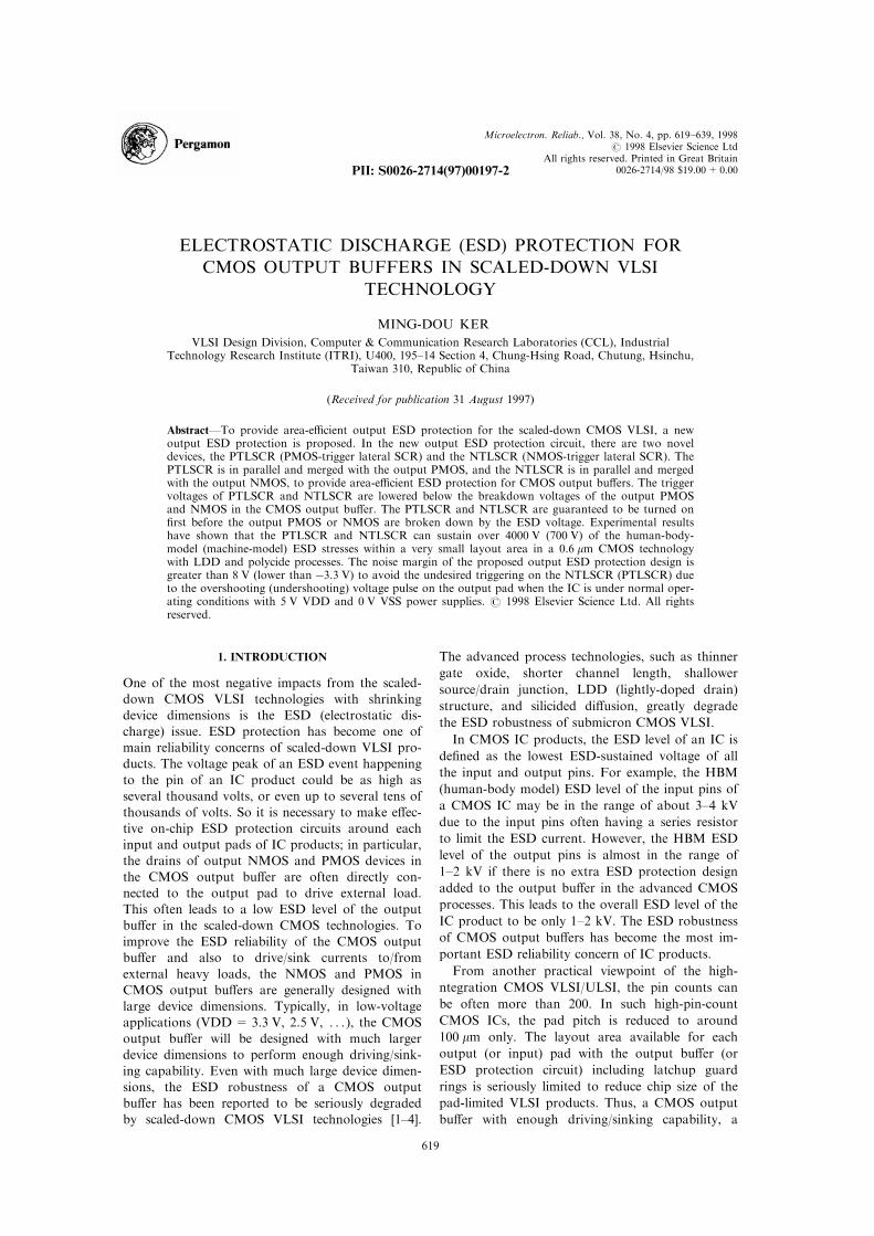
spacer around the gate oxide. The schematic cross-sectional views of the NMOS devices with LDDstructure and ESD-implant structure are shown in
Fig. 1. Because of the lateral-di�usion e�ect in theheavy-doping drain and source regions, the channellength of the ESD-implant output devices has to be
enlarged more than the original design. Forexample, the minimum channel length of the outputNMOS device without the ESD-implant process in
a 0.6 mm CMOS technology is speci®ed by thedesign rules to be 0.8 mm. However, if the outputNMOS device is fabricated with the additionalESD-implant process in the same 0.6 mm CMOS
technology, its channel length has to be longer than
1.2 mm. Therefore, the ESD-implant output NMOS
device has the device structure similar to that of the
early long-channel CMOS technologies. Thus, it
can provide better ESD robustness for submicron
CMOS ICs. A typical experimental result about
the improvement of ESD-implant process on ESD
robustness of the output NMOS device has been
reported in Ref. [14].
Using the ESD-implant process, the ESD re-
liability of the output bu�er can be e�ectively
improved, but the cost of IC fabrication is also
increased by the additional mask and process steps.
Besides, with the ESD-implant process, the channel
length of output device has to be enlarged from 0.8
to 1.2 mm in the 0.6 mm CMOS technology. The
device dimensions of a CMOS output bu�er with
the ESD-implant process have to be re-designed
with one set of ESD-implant SPICE parameters
to calculate the driving/sinking capability. For
example, the output NMOS device with a device
dimension of W/L = 300/0.8 (mm/mm) in the 0.6 mmCMOS technology without the ESD-implant pro-
cess can sink current of 119 mA from the output
pad under the bias conditions of Vgs=5 V and
Vds=5 V. If the output NMOS device is fabricated
with the ESD-implant process in the same 0.6 mmCMOS technology, its device dimension (W/L) has
to be enlarged to 313/1.2 in order to provide the
same sinking current for the output bu�er. Thus,
the layout area of the output bu�er with the
ESD-implant process is also increased. Moreover,
Fig. 1. Schematic cross-sectional view of thin-oxideNMOS device in: (a) an LDD structure; and (b) an ESD-
implant structure.
Ming-Dou Ker620
additional testing devices for the extraction of ESD-implant SPICE parameters have to be included in
the development of ESD-implant process. All ofthese extra e�orts increase the cost and complexityto fabricate CMOS ICs in scaled-down CMOS
technology with the ESD-implant process.
2.2. Additional ESD-protection devices
In some works [19±26], extra ESD-protectionelements have been added to the output pad to
improve ESD robustness of the output bu�er. InRef. [19], an N-well ®eld±oxide device is placed inparallel with the thin-oxide NMOS device of outputbu�er from the output pad to VSS to improve the
ESD robustness of the output bu�er. But thepunch-through voltage of an N-well ®eld±oxidedevice is generally higher than that of the short-
channel thin-oxide NMOS device in scaled-downCMOS technologies and the output NMOS could®rst be damaged before the N-well ®eld-oxide
device is turned on when the ESD stress occurs onthe output pad. Thus, the improvement of ESDprotection by only adding such an N-well ®eld±oxide device may be ine�cient.
In Ref. [20], a lateral n-p-n transistor (like a®eld±oxide device) is placed in parallel with theoutput NMOS to improve ESD robustness of the
CMOS output bu�er. In order to turn on thelateral n-p-n transistor before the snapback break-down of the thin-oxide output NMOS under
ESD-stress conditions, the P+ di�usion for the P-substrate bias is placed away from the lateral n-p-ntransistor to enhance the bipolar action of the
lateral n-p-n transistor. Besides, some P+ di�usionconnected to ground is also placed into the sourceregion of the output NMOS to eliminate theparasitic bipolar snapback action in the thin-oxide
output NMOS device. The voltage di�erence ofsnapback breakdown between the lateral n-p-n tran-sistor and the short-channel thin-oxide output
NMOS device in scaled-down CMOS technologymay be a little, so the output NMOS is still sensi-tive to ESD stress.
In Ref. [21], the CMOS output bu�er is con-nected to the output pad by means of a series resis-tor and two ESD-protection diodes are disposedaround the output pad. This series resistor can pre-
vent ESD damages on the CMOS output bu�erbefore the ESD current is bypassed by the diodes.In Ref. [22], a lateral n-p-n bipolar transistor is
placed in parallel with the output NMOS and aseries polysilicon resistor is connected between theoutput pad and the output bu�er to improve the
ESD reliability of the output bu�er. The lateral n-p-n bipolar transistor can perform e�ective ESD pro-tection only if it can be turned on before the thin-
oxide output NMOS is broken down by the ESDvoltage. In Ref. [23], the large-dimension outputNMOS is separated as several small-dimensionNMOS devices in parallel with each other from the
output pad to ground. There is an extra series
resistor inserted into the drain of each small-dimension NMOS device to improve its ESDrobustness. In particular, the series resistor is
formed by the N-well structure, which is mergedinto the drain structure of the output NMOS. InRef. [24], a thick-oxide snapback device (®eld±oxide
device) is placed in parallel with the output NMOS,and the drain of the output NMOS is modi®ed with
a series N-well resistor as that in Ref. [23] toimprove the ESD reliability of the CMOS outputbu�er. In Refs [21±24], there are series resistors
placed between the output bu�er and the outputpad. These series resistors can e�ectively limit theESD-stress current toward the CMOS output buf-
fer, but they also limit the driving/sinking currentof the CMOS output bu�er. The timing for outputsignal is also delayed by these series resistors. Thus,
the output driving/sinking capability and outputtiming may become out of the original design speci-
®cations. To perform enough driving/sinking capa-bility, the device dimensions of the CMOS outputbu�er have to be enlarged. The CMOS output
bu�er with enlarged device dimension and ad-ditional ESD-protection elements will occupy morelayout area. This limits the applications of Refs
[21±24] in high-speed (minimum delay for output/input signal), high-density (smaller layout area for
the output bu�er), and heavy-loading (high driving/sinking capability) CMOS ICs.In Refs [25] and [26], a modi®ed structure of
lateral SCR device called as LVTSCR (low-voltagetrigger SCR) had been reported to e�ectively pro-tect the output NMOS in submicron CMOS tech-
nology. This LVTSCR device is placed in parallelwith the output NMOS from the output pad to
ground. The LVTSCR device is made by inserting ashort-channel NMOS device into the lateral SCRdevice to lower its trigger voltage. As a positive
ESD voltage occurs at the output pad, this ESDvoltage is diverted to the drain of the short-channelNMOS device in the LVTSCR device and leads to
snapback breakdown on the short-channel NMOSdevice. This snapback breakdown causes the self-
regeneration turn-on action in the LVTSCR device.After the turn-on action, the LVTSCR is held at itslow-impedance state to bypass the ESD current.
The LVTSCR device can provide ESD protectionfor the output NMOS without adding any seriesresistor between the output bu�er and the output
pad.By another method, a dynamic gate-coupled
design [27±30] was reported to improve ESDreliability of large-dimension output NMOS inscaled-down CMOS technology by ensuring uni-
form ESD current ¯ow among the multiple ®ngersof the output NMOS [31]. In Refs [27±29], a para-sitic N-type ®eld±oxide device is connected to the
gate of the output NMOS to achieve uniform ESDpower distribution on the whole output NMOS
Electrostatic discharge protection 621
device. The experimental results showed the uni-
form turn-on phenomenon of the gate-coupled out-put NMOS with a much larger device dimension.To couple suitable ESD-transient voltage to the
gate of the output NMOS, the capacitance ratiobetween the output NMOS and the ®eld±oxidedevice has to be calculated in advance [29].
2.3. Unexpected ESD damages
Since ESD voltages happening to a pin may havepositive or negative polarities with the relatively
grounded VDD or VSS pins, there are four di�erentESD-stress conditions on an output pin as shown inFig. 2:
1. PS-mode, a positive ESD voltage on a pin withthe VSS pin relatively grounded, but the VDDpin and other pins are ¯oating;
2. NS-mode, a negative ESD voltage on a pin withthe VSS pin relatively grounded, but the VDDpin and other pins are ¯oating;
3. PD-mode, a positive ESD voltage on a pin with
the VDD pin relatively grounded, but the VSSpin and other pins are ¯oating;
4. ND-mode, a negative ESD voltage on a pin with
the VDD pin relatively grounded, but the VSSpin and other pins are ¯oating.
The ESD failure threshold of a pin is de®ned as the
lowest (in absolute value) ESD-sustaining voltage ofthe four-mode ESD stresses on the pin. Forexample, if an output pin can sustain even up to 4
kV ESD voltage in the PS-, NS-, and PD-modeESD stresses, but can only sustain 1 kV ESD vol-tage in the ND-mode ESD stress, the ESD failure
threshold for this output pin is de®ned as 1 kVonly. In Refs [19, 20, 22±26, 28] and [29], the ESDprotection is emphasized from the output padto VSS (GND). The additional ESD-protection
elements are all placed from the output pad to
ground in parallel with the output NMOS device.
There is no additional ESD protection element
arranged between the output pad and VDD. Under
the ND- or PD-mode ESD stresses, the output
PMOS (or the output device between VDD and the
output pad) becomes more sensitive to ESD
damage. The overall ESD failure threshold may be
not e�ectively improved. Thus, an e�ective ESD
protection circuit for an output bu�er in scaled-
down CMOS technologies should provide strong
ESD discharging paths from the output pad to
both VSS and VDD.
Moreover, if there is no e�ective ESD-protection
element arranged between the pad and VDD,
an unexpected ESD damage had been found to
locate in the internal circuits beyond the CMOS
output bu�er under the ND-mode ESD stress [32].
Figure 3 shows a schematic diagram to explain the
unexpected discharging paths from the output pad
to the internal circuits of a CMOS IC under the
ND-mode ESD-stress condition. The ND-mode
ESD voltage between the output pad and VDD is
®rst diverted to the ¯oating VSS power line through
the output NMOS before the output PMOS breaks
down to bypass ESD current from the output pad
to VDD. The diverted negative ESD voltage on the
VSS power line will cause voltage stress across the
VSS and VDD power lines. If this ESD voltage
across the VSS and VDD power lines cannot be
e�ectively and quickly bypassed through the VDD-
to-VSS clamp device; this ND-mode ESD voltage
will cause some further unexpected ESD damages
on the internal circuits. Due to the parasitic resist-
ance (RDD and RSS) and capacitance (CDD) along
the VSS and VDD power lines in the CMOS VLSI/
ULSI [33], as well as the voltage drop across the
Fig. 2. The four modes of ESD-stress conditions occurred at an output pin of a CMOS IC.
Ming-Dou Ker622
VDD-to-VSS ESD clamp device, such an ND-modeESD stress had been reported to cause someunexpected ESD damages on the internal circuits
beyond the output bu�er and the ESD protectiondevices [32±35]. Thus, a CMOS output bu�er foradvanced scaled-down CMOS ICs has to provide
e�ective and direct ESD discharging paths from theoutput pad to both VSS and VDD. This is es-pecially necessary for the submicron CMOS VLSI/
ULSI with a larger die size and much longer VDDand VSS power lines which often surround thewhole chip.
3. NEW OUTPUT ESD PROTECTION FOR CMOS
OUTPUT BUFFER
To e�ectively improve ESD robustness of theCMOS output bu�er in submicron CMOS technol-ogies by using the advantages of the LVTSCR
device, a new ESD protection circuit for CMOSoutput bu�er is proposed in this section with theconsideration of avoiding the unexpected ESD
damages in the internal circuits.
3.1. Circuit con®guration
The schematic circuit diagram of the proposed
output ESD protection for the CMOS output bu�eris shown in Fig. 4, where a PTLSCR device(PMOS-trigger lateral SCR) and an NTLSCR
device (NMOS-trigger lateral SCR) are used toprotect the CMOS output bu�er against the four-mode ESD stresses. The PTLSCR (NTLSCR) is
placed in parallel with the output PMOS (NMOS)from the output pad to VDD (VSS). This PTLSCR(NTLSCR) is designed to be turned on before the
output PMOS (NMOS) is broken down by the ND-mode (PS-mode) ESD voltage. Thus, the ESDfailure threshold of the CMOS output bu�er can besigni®cantly improved without using any extra
series resistor between the output bu�er and the
output pad. In the CMOS output bu�er, there also
exist two parasitic junction diodes, Dp and Dn, in
the device structure (the junction between the drain
and the bulk) of the output PMOS and NMOS.
The Dp (Dn) diode is in parallel to the output
PMOS (NMOS) with its anode connected to the
output pad (VSS). In Fig. 4, the PTLSCR
(NTLSCR) is arranged to bypass the ND-mode
(PS-mode) ESD stress, and the Dp (Dn) diode is
used to bypass the PD-mode (NS-mode) ESD
stress.
The trigger voltage of PTLSCR (NTLSCR) is
equivalent to the snapback breakdown voltage of
the inserted short-channel PMOS (NMOS) device
rather than the original switching voltage (about
30±50 V) of a lateral SCR device. The snapback
breakdown voltage of the short-channel thin-oxide
PMOS and NMOS devices is dependent on the
CMOS technology and channel length, but gener-
ally it is lower than the gate±oxide breakdown
voltage in the same CMOS technology. The shorter
Fig. 3. Schematic circuit diagram to show the unexpected ESD damages in the internal circuits beyondthe output bu�er due to the ND-mode ESD stress.
Fig. 4. Schematic circuit diagram of the new proposedESD protection for CMOS output bu�er with the
PTLSCR and NTLSCR devices.
Electrostatic discharge protection 623
channel length leads to a lower snapback break-
down voltage on the thin-oxide NMOS and PMOS
devices. To protect the output NMOS and PMOS,
the channel length of the thin-oxide PMOS
(NMOS) which is inserted in the PTLSCR
(NTLSCR) structure should be designed shorter
than that of the output PMOS (NMOS). Thus, the
trigger voltage of PTLSCR (NTLSCR) can be
lower than the breakdown voltage of the output
PMOS (NMOS) device. When the ND-mode (PS-
mode) ESD events occur on the output pad, the
PTLSCR (NTLSCR) will be ®rst turned on to
bypass ESD current before the output PMOS
(NMOS) is broken down by the ESD voltage.
Thus, the PTLSCR and NTLSCR devices can e�ec-
tively protect the CMOS output bu�er without
adding extra series resistors as those used in Refs
[21±24], and avoid the unexpected ESD damages inthe internal circuits [32±35].
3.2. Device structures
The schematic cross-sectional view of thePTLSCR device merged with the output PMOSdevice to save layout area is shown in Fig. 5(a),where the P-substrate N-well CMOS process is used
to demonstrate the merged device structure. ThePTLSCR is formed by a lateral SCR device with aninserted short-channel thin-oxide PMOS device,
which is used to lower the trigger voltage of thelateral SCR device as shown in the right-hand partof Fig. 5(a). The purpose of inserting a short-chan-
nel thin-oxide PMOS into the lateral SCR structureis to use the drain of the inserted PMOS in its snap-back±breakdown condition to trigger on the lateral
Fig. 5. Schematic cross-sectional views of: (a) the output PMOS and the merged PTLSCR device; and(b) the output NMOS and the merged NTLSCR device, realized in the P-substrate N-well CMOS
process.
Ming-Dou Ker624
SCR structure during the ND-mode ESD stresses.
The inserted PMOS in the PTLSCR is formed by
a non-connection P+ di�usion across the N-well/P-
substrate junction as its drain, the N-well connected
to VDD as its bulk, and a P+ di�usion in the N-
well of bulk as its source. The gate of this inserted
PMOS is connected to VDD to ensure that it is o�
in the normal operating conditions of CMOS ICs.
The trigger voltage of the PTLSCR device is equiv-
alent to the snapback±breakdown voltage of the
inserted PMOS. The holding voltage of PTLSCR
device is still the same as the original holding
voltage (about 1±2 V) of a lateral SCR device with
a very low turn-on resistance (2±5 O) to bypass the
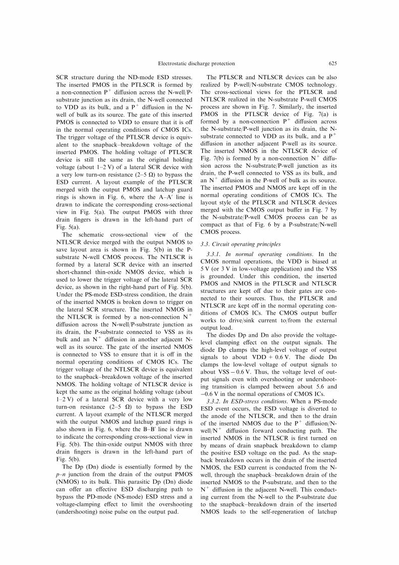
ESD current. A layout example of the PTLSCR
merged with the output PMOS and latchup guard
rings is shown in Fig. 6, where the A±A' line is
drawn to indicate the corresponding cross-sectional
view in Fig. 5(a). The output PMOS with three
drain ®ngers is drawn in the left-hand part of
Fig. 5(a).
The schematic cross-sectional view of the
NTLSCR device merged with the output NMOS to
save layout area is shown in Fig. 5(b) in the P-
substrate N-well CMOS process. The NTLSCR is
formed by a lateral SCR device with an inserted
short-channel thin-oxide NMOS device, which is
used to lower the trigger voltage of the lateral SCR
device, as shown in the right-hand part of Fig. 5(b).
Under the PS-mode ESD-stress condition, the drain
of the inserted NMOS is broken down to trigger on
the lateral SCR structure. The inserted NMOS in
the NTLSCR is formed by a non-connection N+
di�usion across the N-well/P-substrate junction as
its drain, the P-substrate connected to VSS as its
bulk and an N+ di�usion in another adjacent N-
well as its source. The gate of the inserted NMOS
is connected to VSS to ensure that it is o� in the
normal operating conditions of CMOS ICs. The
trigger voltage of the NTLSCR device is equivalent
to the snapback±breakdown voltage of the inserted
NMOS. The holding voltage of NTLSCR device is
kept the same as the original holding voltage (about
1±2 V) of a lateral SCR device with a very low
turn-on resistance (2±5 O) to bypass the ESD
current. A layout example of the NTLSCR merged
with the output NMOS and latchup guard rings is
also shown in Fig. 6, where the B±B' line is drawn
to indicate the corresponding cross-sectional view in
Fig. 5(b). The thin-oxide output NMOS with three
drain ®ngers is drawn in the left-hand part of
Fig. 5(b).
The Dp (Dn) diode is essentially formed by the
p±n junction from the drain of the output PMOS
(NMOS) to its bulk. This parasitic Dp (Dn) diode
can o�er an e�ective ESD discharging path to
bypass the PD-mode (NS-mode) ESD stress and a
voltage-clamping e�ect to limit the overshooting
(undershooting) noise pulse on the output pad.
The PTLSCR and NTLSCR devices can be alsorealized by P-well/N-substrate CMOS technology.
The cross-sectional views for the PTLSCR andNTLSCR realized in the N-substrate P-well CMOSprocess are shown in Fig. 7. Similarly, the inserted
PMOS in the PTLSCR device of Fig. 7(a) isformed by a non-connection P+ di�usion acrossthe N-substrate/P-well junction as its drain, the N-
substrate connected to VDD as its bulk, and a P+
di�usion in another adjacent P-well as its source.The inserted NMOS in the NTLSCR device of
Fig. 7(b) is formed by a non-connection N+ di�u-sion across the N-substrate/P-well junction as itsdrain, the P-well connected to VSS as its bulk, andan N+ di�usion in the P-well of bulk as its source.
The inserted PMOS and NMOS are kept o� in thenormal operating conditions of CMOS ICs. Thelayout style of the PTLSCR and NTLSCR devices
merged with the CMOS output bu�er in Fig. 7 bythe N-substrate/P-well CMOS process can be ascompact as that of Fig. 6 by a P-substrate/N-well
CMOS process.
3.3. Circuit operating principles
3.3.1. In normal operating conditions. In theCMOS normal operations, the VDD is biased at5 V (or 3 V in low-voltage application) and the VSS
is grounded. Under this condition, the insertedPMOS and NMOS in the PTLSCR and NTLSCRstructures are kept o� due to their gates are con-
nected to their sources. Thus, the PTLSCR andNTLSCR are kept o� in the normal operating con-ditions of CMOS ICs. The CMOS output bu�er
works to drive/sink current to/from the externaloutput load.The diodes Dp and Dn also provide the voltage-
level clamping e�ect on the output signals. The
diode Dp clamps the high-level voltage of outputsignals to about VDD+ 0.6 V. The diode Dnclamps the low-level voltage of output signals to
about VSSÿ 0.6 V. Thus, the voltage level of out-put signals even with overshooting or undershoot-ing transition is clamped between about 5.6 and
ÿ0.6 V in the normal operations of CMOS ICs.3.3.2. In ESD-stress conditions. When a PS-mode
ESD event occurs, the ESD voltage is diverted tothe anode of the NTLSCR, and then to the drain
of the inserted NMOS due to the P+ di�usion/N-well/N+ di�usion forward conducting path. Theinserted NMOS in the NTLSCR is ®rst turned on
by means of drain snapback breakdown to clampthe positive ESD voltage on the pad. As the snap-back breakdown occurs in the drain of the inserted
NMOS, the ESD current is conducted from the N-well, through the snapback±breakdown drain of theinserted NMOS to the P-substrate, and then to the
N+ di�usion in the adjacent N-well. This conduct-ing current from the N-well to the P-substrate dueto the snapback±breakdown drain of the insertedNMOS leads to the self-regeneration of latchup
Electrostatic discharge protection 625
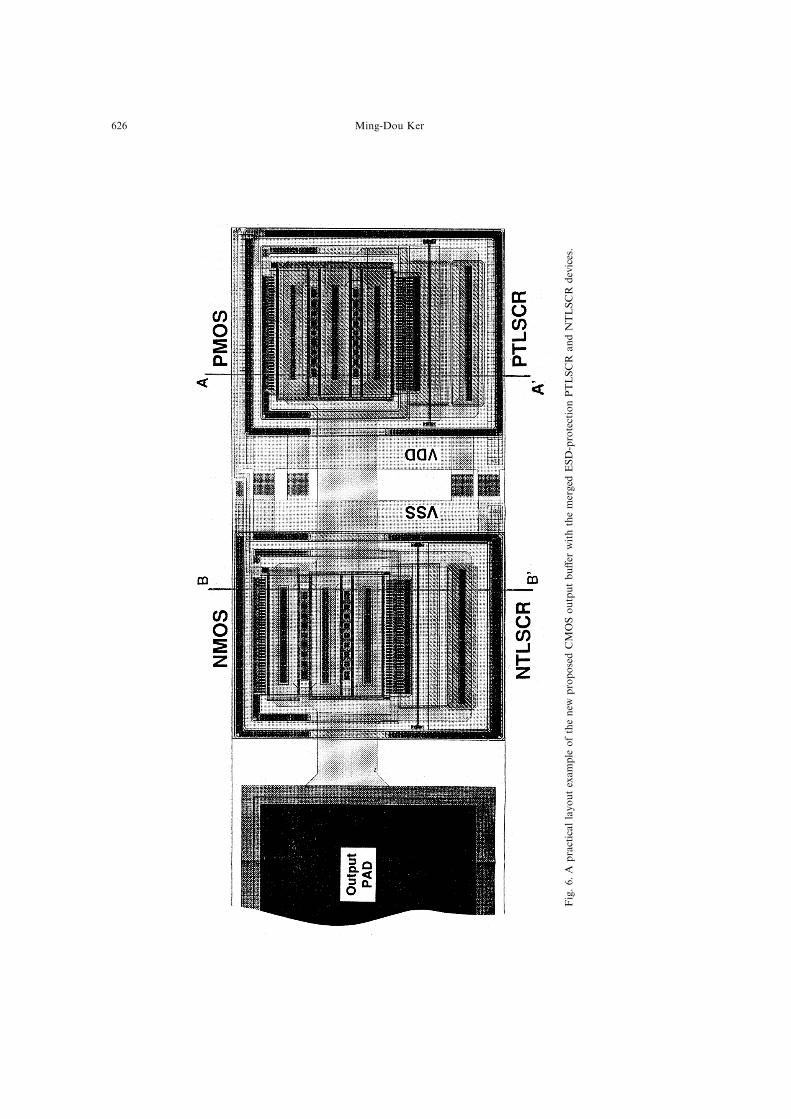
Fig.6.A
practicallayoutexample
ofthenew
proposedCMOSoutputbu�er
withthemerged
ESD-protectionPTLSCR
andNTLSCR
devices.
Ming-Dou Ker626
happening in the NTLSCR device. Once the
latchup happens in the NTLSCR, a path with very
low impedance from the output pad to VSS (GND)
is created. Then, the ESD current is mainly dis-
charged through the lateral SCR structure of the
NTLSCR device. The ESD voltage on the output
pad becomes clamped by the holding voltage of the
turn-on lateral SCR structure to about 1±2 V. This
NTLSCR device can e�ectively protect the CMOS
output bu�er against the PS-mode ESD damages
alone without adding any extra series resistor. Due
to the high capability of power delivery in the SCR
device, the NTLSCR with a lower trigger voltage
can sustain a higher ESD-stress current in a small
layout area.
In the NS-mode (PD-mode) ESD event, the ESD
stress with negative (positive) voltage occurs at the
output pad and the VSS (VDD) is grounded but
the VDD (VSS) is ¯oating. The negative (positive)
ESD voltage is diverted to the drain of the output
NMOS (PMOS). The parasitic diode Dn (Dp) in
the output NMOS (PMOS) is forward biased and
turned on to bypass ESD current. The negative
(positive) ESD voltage on the output pad is
clamped by the turn-on diode Dn (Dp) to about
ÿ0.6 V (+0.6 V) so as to protect the output bu�er.
The diode Dn (Dp) in its forward-conducting
condition can sustain very high ESD current.
When the ND-mode ESD event occurs at the
output pad with negative polarity to the grounded
VDD, but the VSS is ¯oating, the ESD voltage is
diverted to the cathode of the PTLSCR, and then
to the drain of the inserted PMOS through the P+
di�usion/P-substrate/N-well/N+ di�usion forward-
Fig. 7. Schematic cross-sectional views of: (a) the output PMOS and the merged PTLSCR device; and(b) the output NMOS and the merged NTLSCR device, realized in the N-substrate P-well CMOS
process.
Electrostatic discharge protection 627
conducting path. The inserted PMOS in thePTLSCR is ®rst turned on by means of drain
snapback±breakdown to clamp the negative ESDvoltage on the output pad. As the snapback±breakdown occurs in the drain of the inserted
PMOS, the ESD current is conducted from the P+
di�usion (the anode of PTLSCR, connected toVDD), through the snapback±breakdown drain ofthe inserted PMOS to the P-substrate, and then to
the N+ di�usion in the adjacent N-well connectedto the output pad. This conducting current fromthe N-well to the P-substrate due to the snapback±
breakdown drain of the inserted PMOS leads to theself-regeneration of latchup happening in thePTLSCR device. Once the latchup happens in the
PTLSCR, a path with very low impedance fromVDD to the output pad is created. Then, the ESDcurrent is mainly discharged through the lateral
SCR structure of the PTLSCR device. The ESDvoltage on the output pad becomes clamped by theholding voltage of the turn-on lateral SCR structureto about 1 to 2 V. This PTLSCR can e�ectively
protect the CMOS output bu�er against ND-modeESD damages alone without adding any extra seriesresistor. Due to the high capability of power
delivery in SCR device, the PTLSCR with a lowertrigger voltage can sustain a high ESD-stresscurrent in a small layout area.
4. EXPERIMENTAL RESULTS
4.1. ESD reliability
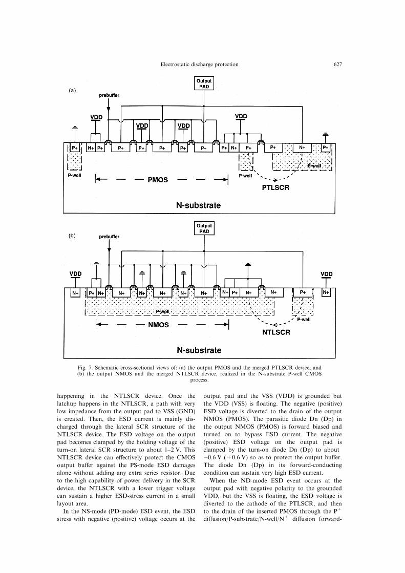
One set of test-keys is fabricated by a 0.6 mmsingle-poly three-metal CMOS technology withLDD and polycide processes to verify this outputESD protection design, in which a modi®ed CMOS
output bu�er with the N-well resistor [23] is also
fabricated as a comparing reference. The device's
width and length in the output PMOS (NMOS) of
the modi®ed CMOS output bu�er are 300 and 1.0(200 and 1.0) mm, respectively. The schematic cross-
sectional view of the modi®ed CMOS output bu�er
with the N-well resistor is shown in Fig. 8, where
the drain of the output NMOS is connected to the
output pad through an N-well structure. The layout
area of the output PMOS (NMOS) including the
latchup guard rings in the modi®ed CMOS output
bu�er is 112.6�52 (136.2�52) mm2.
Corresponding to the layout in Fig. 6, the output
bu�er protected by the PTLSCR and NTLSCR has
a device W/L of 312/1.0 (300/1.0) for the output
PMOS (NMOS), whereas the inserted PMOS(NMOS) to trigger on the PTLSCR (NTLSCR) has
a device W/L of 60/0.8 (60/0.8). The total layout
area for the output PMOS (NMOS) with the
merged PTLSCR (NTLSCR) including latchup
guard rings is 107.4�86 (111.4�86) mm2.
However, the PTLSCR (NTLSCR) only occupies a
layout area of 60� 37 (60� 38) mm2 in Fig. 6. Asexpected by this design, the PTLSCR (NTLSCR)
can be turned on to protect the output PMOS
(NMOS) in the ND-mode (PS-mode) ESD-stress
conditions. The PTLSCR (NTLSCR) can provide
high ESD protection level to the CMOS output
bu�er, but it only occupies very small layout area.
The typical ESD testing results are shown in
Table 1.
The ESD-stress voltage is set to begin with an
initial voltage of 1000 V and increase up to 8000 V
with an increase step of 250 V in the human-body-
model (HBM) ESD testing. The machine-model(MM) ESD stress with faster ESD-transient
conditions is also used to investigate the ESD
Fig. 8. The schematic cross-sectional view of a CMOS output bu�er with the N-well resistor [23].
Ming-Dou Ker628
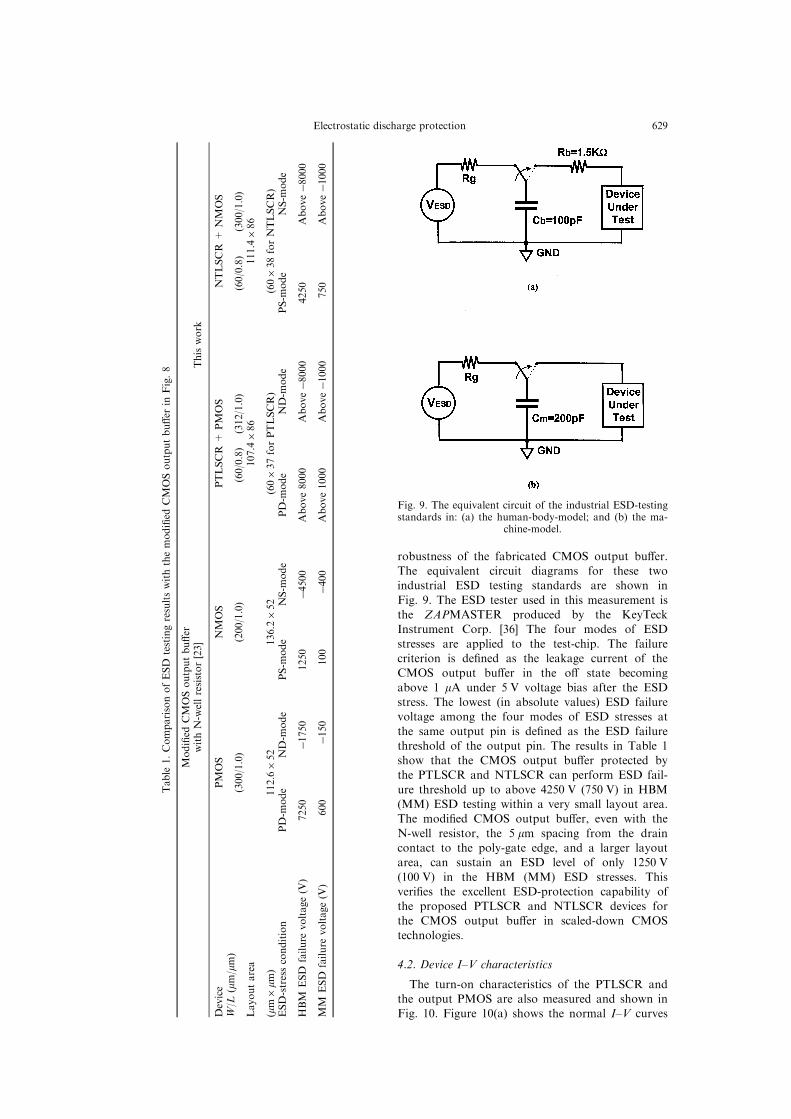
robustness of the fabricated CMOS output bu�er.The equivalent circuit diagrams for these twoindustrial ESD testing standards are shown in
Fig. 9. The ESD tester used in this measurement isthe ZAPMASTER produced by the KeyTeckInstrument Corp. [36] The four modes of ESD
stresses are applied to the test-chip. The failurecriterion is de®ned as the leakage current of theCMOS output bu�er in the o� state becoming
above 1 mA under 5 V voltage bias after the ESDstress. The lowest (in absolute values) ESD failurevoltage among the four modes of ESD stresses at
the same output pin is de®ned as the ESD failurethreshold of the output pin. The results in Table 1show that the CMOS output bu�er protected bythe PTLSCR and NTLSCR can perform ESD fail-
ure threshold up to above 4250 V (750 V) in HBM(MM) ESD testing within a very small layout area.The modi®ed CMOS output bu�er, even with the
N-well resistor, the 5 mm spacing from the draincontact to the poly-gate edge, and a larger layoutarea, can sustain an ESD level of only 1250 V
(100 V) in the HBM (MM) ESD stresses. Thisveri®es the excellent ESD-protection capability ofthe proposed PTLSCR and NTLSCR devices forthe CMOS output bu�er in scaled-down CMOS
technologies.
4.2. Device I±V characteristics
The turn-on characteristics of the PTLSCR andthe output PMOS are also measured and shown inFig. 10. Figure 10(a) shows the normal I±V curves
Table
1.ComparisonofESD
testingresultswiththemodi®ed
CMOSoutputbu�er
inFig.8
Modi®ed
CMOSoutputbu�er
withN-w
ellresistor[23]
Thiswork
Device
PMOS
NMOS
PTLSCR
+PMOS
NTLSCR
+NMOS
W/L
(mm/mm)
(300/1.0)
(200/1.0)
(60/0.8)
(312/1.0)
(60/0.8)
(300/1.0)
Layoutarea
107.4�86
111.4�86
(mm�mm
)112.6�52
136.2�52
(60�37forPTLSCR)
(60�38forNTLSCR)
ESD-stresscondition
PD-m
ode
ND-m
ode
PS-m
ode
NS-m
ode
PD-m
ode
ND-m
ode
PS-m
ode
NS-m
ode
HBM
ESD
failure
voltage(V
)7250
ÿ1750
1250
ÿ4500
Above8000
Aboveÿ8
000
4250
Aboveÿ8
000
MM
ESD
failure
voltage(V
)600
ÿ150
100
ÿ400
Above1000
Aboveÿ1
000
750
Aboveÿ1
000
Fig. 9. The equivalent circuit of the industrial ESD-testingstandards in: (a) the human-body-model; and (b) the ma-
chine-model.
Electrostatic discharge protection 629
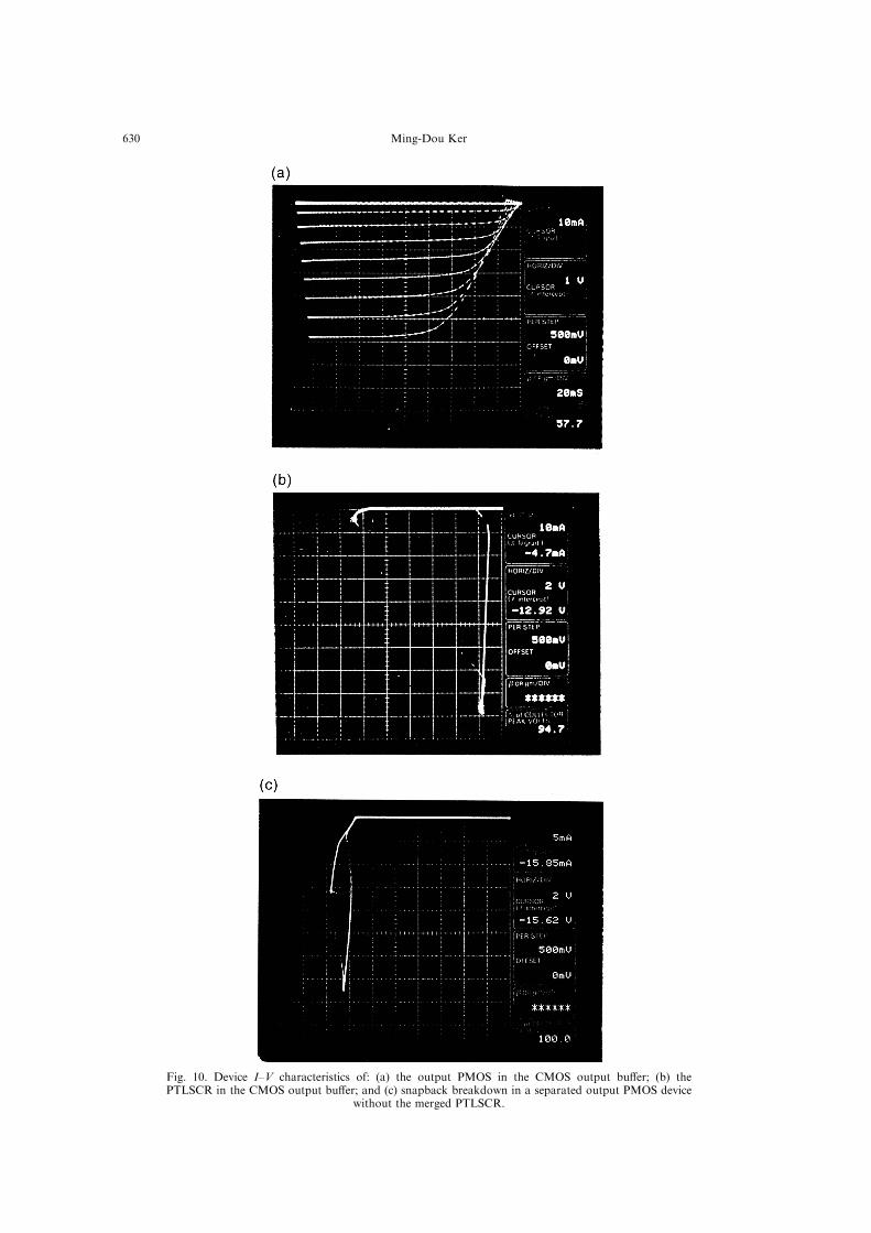
Fig. 10. Device I±V characteristics of: (a) the output PMOS in the CMOS output bu�er; (b) thePTLSCR in the CMOS output bu�er; and (c) snapback breakdown in a separated output PMOS device
without the merged PTLSCR.
Ming-Dou Ker630
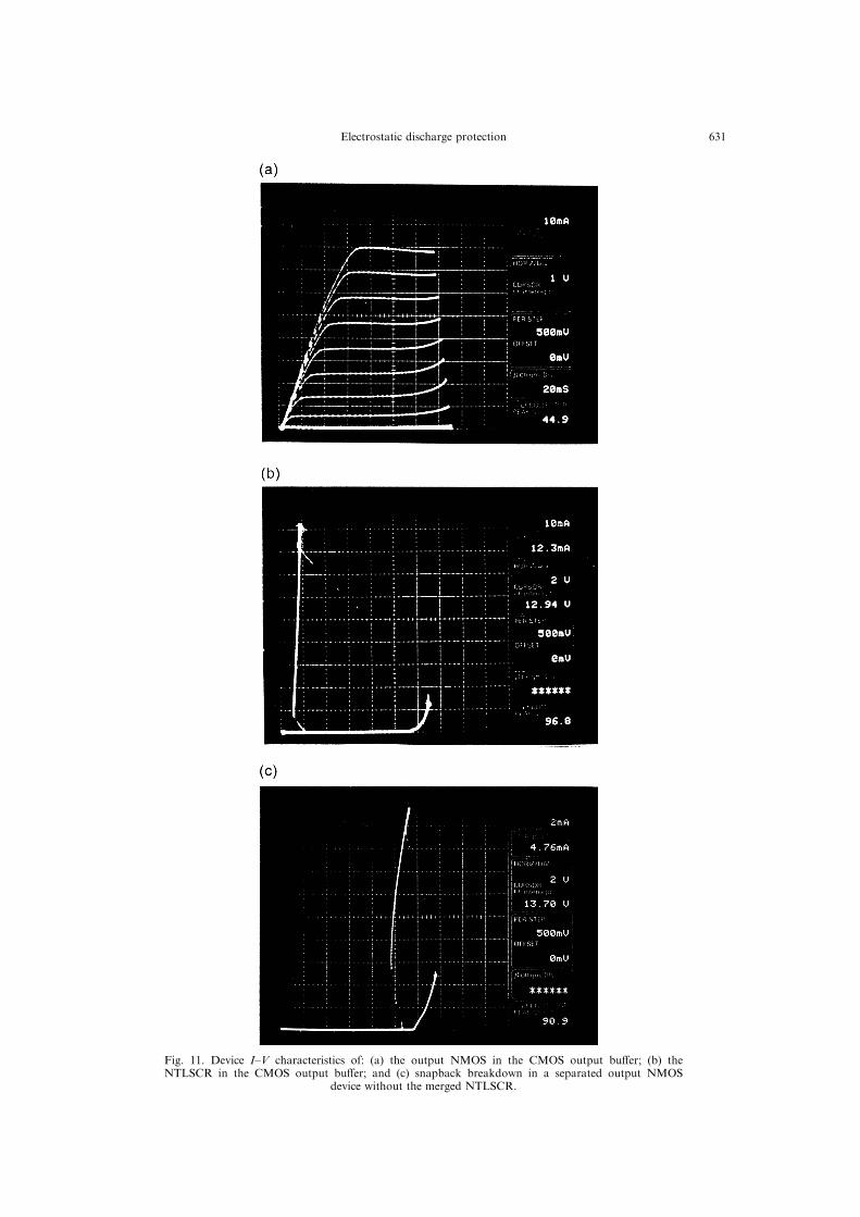
Fig. 11. Device I±V characteristics of: (a) the output NMOS in the CMOS output bu�er; (b) theNTLSCR in the CMOS output bu�er; and (c) snapback breakdown in a separated output NMOS
device without the merged NTLSCR.
Electrostatic discharge protection 631
of the output PMOS under di�erent Vgs biases in
the CMOS output bu�er of Fig. 5(a) with thePTLSCR. With a Vds of up to ÿ10 V applied to thedrain of the output PMOS, the I±V curves of
PMOS as shown in Fig. 10(a) are still not a�ectedby the PTLSCR. Thus, the PMOS device in theCMOS output bu�er can normally perform the
driving current to the output pad without anydegradation by the PTLSCR. If the gate of the
output PMOS is connected to its source and anND-mode voltage is applied to the output pad, theI±V curves of the PTLSCR can be measured and
are shown in Fig. 10(b). This means that thePTLSCR is triggered on before the breakdown ofthe output PMOS. The trigger voltage (current) of
the PTLSCR is ÿ12.92 V (ÿ4.7 mA), and its hold-ing voltage (current) is ÿ1.24 V (ÿ7.5 mA). The
channel length of the inserted PMOS in thePTLSCR is 0.8 mm. To verify that the PTLSCR isindeed triggered on before the output PMOS breaks
down, a separated PMOS device without thePTLSCR has to be also fabricated in the same test-chip to ®nd the snapback±breakdown character-
istics of the pure output PMOS. The snapback±breakdown I±V curve of the pure PMOS device
with a channel length of 1.0 mm is shown inFig. 10(c), which is measured by applying a nega-tive voltage to the drain of the PMOS device with
its gate and source connected to ground. Thetrigger voltage (current) of the snapback breakdownin the output PMOS is ÿ15.62 V (ÿ15.85 mA). The
holding voltage (current) of the output PMOS in itssnapback region is ÿ13.84 V (ÿ13.9 mA). Because
the trigger voltage and current of the output PMOSinto its snapback region is greater than that of thePTLSCR into its latching state, the PTLSCR has
been con®rmed to be turned on before the outputPMOS breaks down. Thus, under the ND-modeESD-stress condition, the PTLSCR is guaranteed
to be ®rst turned on to protect the CMOS outputbu�er.
The turn-on characteristics of the NTLSCR andthe output NMOS devices in the CMOS outputbu�er are also measured and are shown in Fig. 11.
The I±V curves of the output NMOS in the CMOSoutput bu�er with the NTLSCR under the normal
operation conditions are shown in Fig. 11(a). TheI±V curve of the NTLSCR in the CMOS outputbu�er is shown in Fig. 11(b). The channel length of
the inserted NMOS in the NTLSCR is 0.8 mm. Thetrigger voltage (current) of the NTLSCR is 12.94 V(12.3 mA) and its holding voltage (current) is 1.1 V
(6.9 mA). The snapback±breakdown characteristicsof a pure NMOS device with the channel length of
1.0 mm in the CMOS output bu�er is shown inFig. 11(c). The trigger voltage (current) of thesnapback breakdown in the output NMOS is
13.7 V (4.76 mA). The holding voltage (current) ofthe output NMOS in its snapback region is 9.78 V(5.42 mA). Comparing the I±V curves between
Fig. 11(b) and (c), it can be guaranteed that theNTLSCR can be ®rst turned on before the output
NMOS is broken down under the PS-mode ESD-stress condition. The holding voltage of theNTLSCR is also much smaller than the snapback
voltage of the NMOS in the CMOS output bu�er.Thus, the NTLSCR can e�ectively protect theCMOS output bu�er against ESD damage.
4.3. Pulse-type triggering characteristics
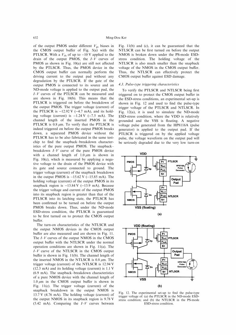
To verify the PTLSCR and NTLSCR being ®rsttriggered on to protect the CMOS output bu�er in
the ESD-stress conditions, an experimental set-up isshown in Fig. 12 and used to ®nd the pulse-typetrigger voltage of the PTLSCR and NTLSCR. In
Fig. 12(a), it is used to simulate the ND-modeESD-stress condition, where the VDD is relativelygrounded and the VSS is ¯oating. A negativevoltage pulse generated from the HP8116A (pulse
generator) is applied to the output pad. If thePTLSCR is triggered on by the applied voltagepulse, the voltage waveform on the output pad will
be seriously degraded due to the very low turn-on
Fig. 12. The experimental set-up to ®nd the pulse-typetrigger voltage of: (a) the PTLSCR in the ND-mode ESD-stress condition; and (b) the NTLSCR in the PS-mode
ESD-stress condition.
Ming-Dou Ker632
resistance of the PTLSCR and the voltage level on
the output pad will be clamped near to the holding
voltage ( 0ÿ 2 V) of the PTLSCR. If the output
PMOS is ®rst triggered on, the voltage on the out-
put pad will be clamped by the snapback voltage
(about 0ÿ 14 V) of the output PMOS. However,
if neither the PTLSCR nor the output PMOS is
triggered on, the voltage waveform on the output
pad will remain the same. The measured results are
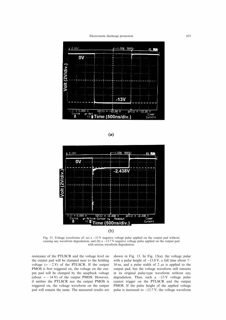
shown in Fig. 13. In Fig. 13(a), the voltage pulse
with a pulse height of ÿ13.0 V, a fall time about 7±
10 ns, and a pulse width of 2 ms is applied to the
output pad, but the voltage waveform still remains
in its original pulse-type waveform without any
degradation. Thus, such a ÿ13 V voltage pulse
cannot trigger on the PTLSCR and the output
PMOS. If the pulse height of the applied voltage
pulse is increased to ÿ13.7 V, the voltage waveform
Fig. 13. Voltage waveforms of: (a) a ÿ13 V negative voltage pulse applied on the output pad withoutcausing any waveform degradation; and (b) a ÿ13.7 V negative voltage pulse applied on the output pad
with serious waveform degradation.
Electrostatic discharge protection 633
on the output pad is measured and shown in
Fig. 13(b), where the voltage waveform is seriously
degraded. As shown in Fig. 13(b), the falling edge
of the applied negative voltage pulse triggers on
the PTLSCR and causes a voltage clamp about
ÿ2.438 V on the output pad. Thus, the PTLSCR
has been further veri®ed to be triggered on before
the output PMOS breaks down in the ND-mode
ESD-stress condition. With such a low clamping
voltage, the CMOS output bu�er can be fully
protected by the PTLSCR.
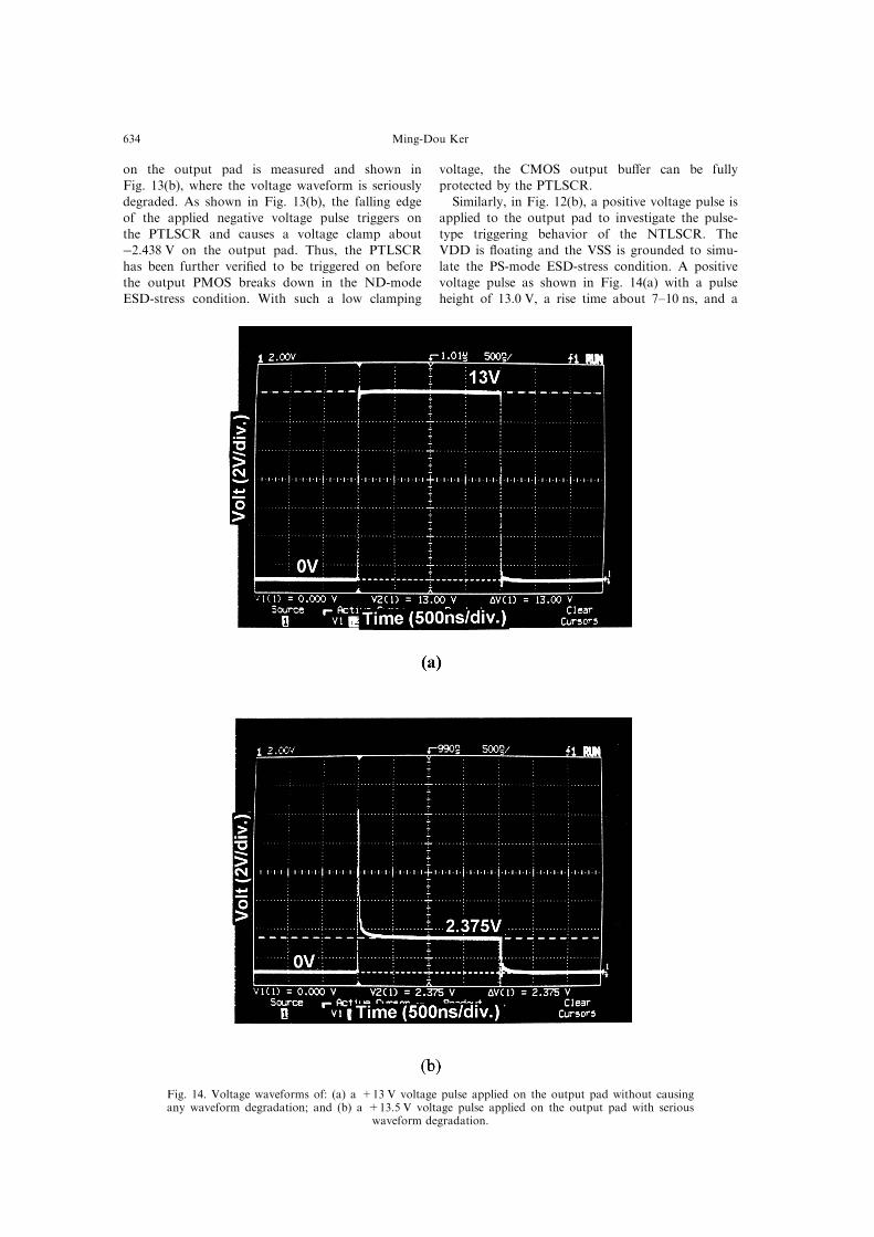
Similarly, in Fig. 12(b), a positive voltage pulse is
applied to the output pad to investigate the pulse-
type triggering behavior of the NTLSCR. The
VDD is ¯oating and the VSS is grounded to simu-
late the PS-mode ESD-stress condition. A positive
voltage pulse as shown in Fig. 14(a) with a pulse
height of 13.0 V, a rise time about 7±10 ns, and a
Fig. 14. Voltage waveforms of: (a) a +13 V voltage pulse applied on the output pad without causingany waveform degradation; and (b) a +13.5 V voltage pulse applied on the output pad with serious
waveform degradation.
Ming-Dou Ker634
pulse width of 2 ms is applied to the output pad,but the voltage waveform still remains in its original
pulse-type waveform without any degradation. So,such a 13 V voltage pulse cannot trigger on theNTLSCR and the output NMOS. If the pulse
height of the applied voltage pulse is increased to13.5 V, the voltage waveform on the output pad ismeasured and shown in Fig. 14(b), where the
voltage waveform is seriously degraded. The risingedge of the positive voltage pulse triggers on theNTLSCR and clamps the voltage level on the out-
put pad at 2.375 V. Thus, the NTLSCR has beenfurther veri®ed to be triggered on before the outputNMOS breaks down in the PS-mode ESD-stresscondition. With such a low clamping voltage, the
CMOS output bu�er can be fully protected by theNTLSCR.
4.4. Noise margin in the normal operating conditions
The PTLSCR and NTLSCR are designed to be
triggered on only in the ESD-stress conditions, butto be kept o� in the normal operating conditions ofthe CMOS IC with 5 V VDD and 0 V VSS powersupplies. However, in practical applications, there
may be some overshooting or undershooting noisepulses attaching to the output pad. Therefore, thePTLSCR and NTLSCR should have a suitable
noise margin to the output overshooting or under-shooting noise pulses that is dependent on theapplication environment of the IC. To investigate
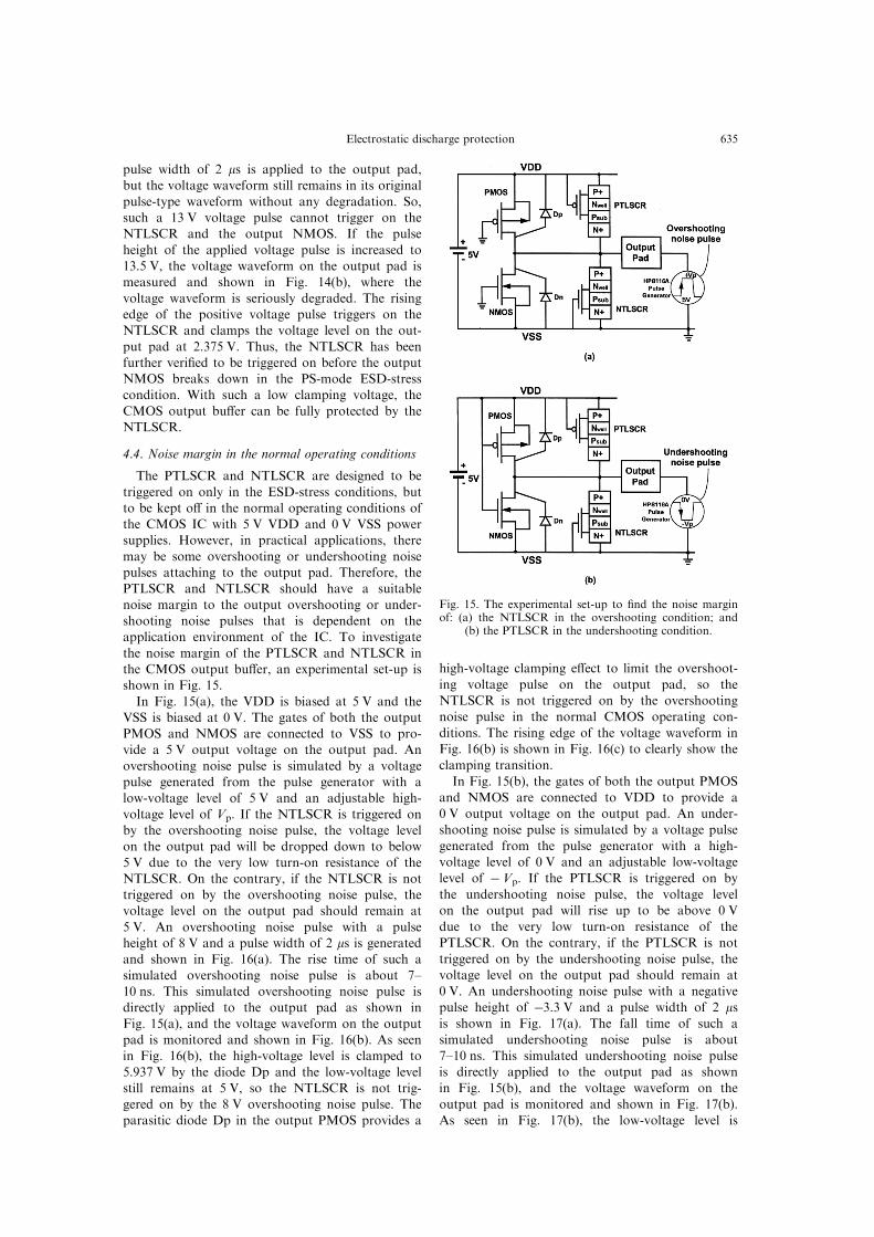
the noise margin of the PTLSCR and NTLSCR inthe CMOS output bu�er, an experimental set-up isshown in Fig. 15.
In Fig. 15(a), the VDD is biased at 5 V and theVSS is biased at 0 V. The gates of both the outputPMOS and NMOS are connected to VSS to pro-vide a 5 V output voltage on the output pad. An
overshooting noise pulse is simulated by a voltagepulse generated from the pulse generator with alow-voltage level of 5 V and an adjustable high-
voltage level of Vp. If the NTLSCR is triggered onby the overshooting noise pulse, the voltage levelon the output pad will be dropped down to below
5 V due to the very low turn-on resistance of theNTLSCR. On the contrary, if the NTLSCR is nottriggered on by the overshooting noise pulse, thevoltage level on the output pad should remain at
5 V. An overshooting noise pulse with a pulseheight of 8 V and a pulse width of 2 ms is generatedand shown in Fig. 16(a). The rise time of such a
simulated overshooting noise pulse is about 7±10 ns. This simulated overshooting noise pulse isdirectly applied to the output pad as shown in
Fig. 15(a), and the voltage waveform on the outputpad is monitored and shown in Fig. 16(b). As seenin Fig. 16(b), the high-voltage level is clamped to
5.937 V by the diode Dp and the low-voltage levelstill remains at 5 V, so the NTLSCR is not trig-gered on by the 8 V overshooting noise pulse. Theparasitic diode Dp in the output PMOS provides a
high-voltage clamping e�ect to limit the overshoot-
ing voltage pulse on the output pad, so theNTLSCR is not triggered on by the overshooting
noise pulse in the normal CMOS operating con-
ditions. The rising edge of the voltage waveform inFig. 16(b) is shown in Fig. 16(c) to clearly show the
clamping transition.
In Fig. 15(b), the gates of both the output PMOS
and NMOS are connected to VDD to provide a0 V output voltage on the output pad. An under-
shooting noise pulse is simulated by a voltage pulse
generated from the pulse generator with a high-voltage level of 0 V and an adjustable low-voltage
level of ÿVp. If the PTLSCR is triggered on by
the undershooting noise pulse, the voltage levelon the output pad will rise up to be above 0 V
due to the very low turn-on resistance of the
PTLSCR. On the contrary, if the PTLSCR is not
triggered on by the undershooting noise pulse, thevoltage level on the output pad should remain at
0 V. An undershooting noise pulse with a negative
pulse height of ÿ3.3 V and a pulse width of 2 msis shown in Fig. 17(a). The fall time of such a
simulated undershooting noise pulse is about
7±10 ns. This simulated undershooting noise pulseis directly applied to the output pad as shown
in Fig. 15(b), and the voltage waveform on the
output pad is monitored and shown in Fig. 17(b).As seen in Fig. 17(b), the low-voltage level is
Fig. 15. The experimental set-up to ®nd the noise marginof: (a) the NTLSCR in the overshooting condition; and
(b) the PTLSCR in the undershooting condition.
Electrostatic discharge protection 635
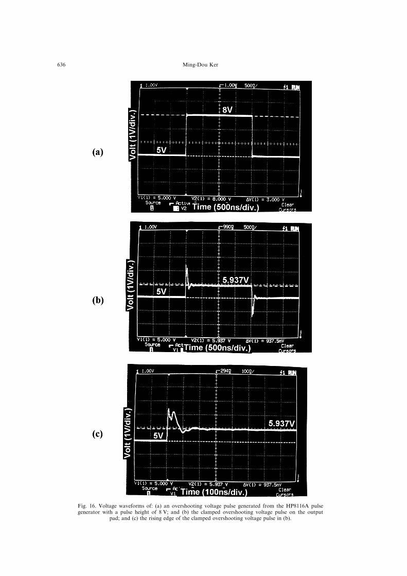
Fig. 16. Voltage waveforms of: (a) an overshooting voltage pulse generated from the HP8116A pulsegenerator with a pulse height of 8 V; and (b) the clamped overshooting voltage pulse on the output
pad; and (c) the rising edge of the clamped overshooting voltage pulse in (b).
Ming-Dou Ker636
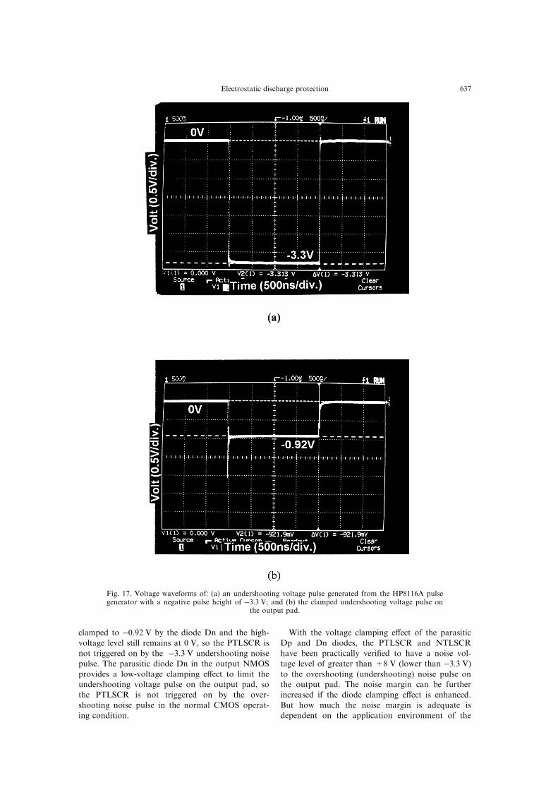
clamped to ÿ0.92 V by the diode Dn and the high-
voltage level still remains at 0 V, so the PTLSCR is
not triggered on by the ÿ3.3 V undershooting noise
pulse. The parasitic diode Dn in the output NMOS
provides a low-voltage clamping e�ect to limit the
undershooting voltage pulse on the output pad, so
the PTLSCR is not triggered on by the over-
shooting noise pulse in the normal CMOS operat-
ing condition.
With the voltage clamping e�ect of the parasitic
Dp and Dn diodes, the PTLSCR and NTLSCR
have been practically veri®ed to have a noise vol-
tage level of greater than +8 V (lower than ÿ3.3 V)to the overshooting (undershooting) noise pulse on
the output pad. The noise margin can be further
increased if the diode clamping e�ect is enhanced.
But how much the noise margin is adequate is
dependent on the application environment of the
Fig. 17. Voltage waveforms of: (a) an undershooting voltage pulse generated from the HP8116A pulsegenerator with a negative pulse height of ÿ3.3 V; and (b) the clamped undershooting voltage pulse on
the output pad.
Electrostatic discharge protection 637
IC. In the most applications of CMOS ICs with a5 V power supply, a voltage margin of +8 V
(ÿ3.3 V) to the overshooting (undershooting) noisepulse has been a reasonable design.
4.5. Discussion on layout spacing in the output bu�er
For better ESD robustness consideration, thelayout spacing `` d'' from the drain contact to the
poly-gate edge is often drawn as 5 mm in the outputNMOS and PMOS [14, 37]. Suitably spaced d canhelp the uniform current distribution among the
drain contacts of the ®ngers in the ®nger-typelayout to improve the ESD level of the outputbu�er. But a wider layout spacing d causes the out-put bu�er to occupy a larger layout area.
Because the channel length of the insertedNMOS/PMOS in the NTLSCR/PTLSCR is shorterthan that of the output bu�er, the NTLSCR/
PTLSCR can be triggered on to protect the outputbu�er before the output bu�er is damaged by theESD pulse. The turn-on speed of the PTLSCR/
NTLSCR has been practically veri®ed in Figs 13and 14 in the ND- and PS-mode ESD-stress con-ditions, respectively. As shown in Fig. 13(b) and
14(b), the PTLSCR (NTLSCR) can be immediatelytriggered on by the applied negative (positive)voltage pulse. Therefore, the spacing d in the outputbu�er which is protected by such PTLSCR/
NTLSCR can be reasonably reduced from 5 mm toabout 1 mm to further save the layout area.
5. CONCLUSION
A robust output ESD protection has beendesigned and veri®ed in an advanced 0.6 mmCMOS process. The trigger voltage of PTLSCR
(NTLSCR) is lowered to the snapback±triggervoltage of a short-channel thin-oxide PMOS(NMOS) device inserted into the SCR structure.
However, the holding voltage of PTLSCR andNTLSCR devices is still the same as that of a lat-eral SCR device. The PTLSCR and NTLSCR
devices with enough lower trigger voltage can e�ec-tively protect the CMOS output bu�er within asmall layout area than other output ESD protectioncircuits in submicron CMOS ICs. The PTLSCR
and NTLSCR provide the CMOS output bu�erwith direct ESD discharging paths and low clamp-ing voltage levels from the output pad to both
VDD and VSS, so the unexpected ESD damages inthe internal circuits can be avoided. This ESD pro-tection circuit can be also free to the VDD-to-VSS
latchup problem in 5 V CMOS ICs. Under the 5 VCMOS operating conditions, the CMOS outputbu�er has a noise margin greater than +8 V (lower
than ÿ3.3 V) to the overshooting (undershooting)noise pulse for practical applications withoutthe undesired triggering on the PTLSCR andNTLSCR. One set of area-e�cient CMOS output
bu�ers with di�erent driving speci®cations has beendesigned with this ESD protection circuit and
included into a 0.6 mm CMOS standard cell libraryfor chip synthesis. It has been successfully used insome ASICs to provide the output function with an
operating frequency of up to 50 MHz.With a high ESD failure threshold in a small
layout area and without adding any extra series
resistor between the output pad and the outputbu�er, this proposed output ESD protection designprovides an e�ective ESD protection to the CMOS
output bu�er without causing any degradation onthe circuit performance or the output voltage leveland timing speci®cations. Thus, this proposed out-put ESD protection design is very suitable for the
scaled-down CMOS VLSI in high-reliability, high-density and high-speed applications.
REFERENCES
1. Duvvury, C., Rountree, R. N., Fong, Y. and McPhee,R. A., in Proceedings of the IRPS, 1987, pp. 174±180.
2. Duvvury, C. and Amerasekera, A., in Proceedings ofthe IEEE, 81, 1993, pp. 690±702.
3. Amerasekera, A. and Duvvury, C., in Proceedings ofthe EOS/ESD Symposium, 1994, pp. 237±245.
4. Duvvury, C., McPhee, R., Baglee, D. and Rountree,R., in Proceedings of the IRPS, 1986, pp. 199±205.
5. Rountree, R. N., IEDM Technical Digest, 1988, pp.580±583.
6. Duvvury, C. and Rountree, R. N., in Proceedings ofthe EOS/ESD Symposium, 1991, pp. 88±97.
7. Wu, C-Y., Ker, M-D., Lee, C-Y. and Ko, J., IEEEJournal of Solid-State Circuits, 1992, 27, 274±280.
8. Ker, M-D. and Wu, C-Y., IEEE Transactions onElectronic Devices, 1995, 42, 1297±1304.
9. Ker, M-D., Wu, C-Y., Cheng, T., Wu, M., Yu, T-L.and Wang, A., in Proceedings of the IEEEInternational Integrated Reliability Workshop, 1994,pp. 124±128.
10. Ker, M-D., Wang, K-F., Joe, M-C., Chu, Y-H. andWu, T-S., in Proceedings of the 8th IEEE InternationalASIC Conference and Exhibition, 1995, pp. 123±126.
11. Hu, C., Tam, S. C., Hsu, F-C., Ko, P. K., Chan, T.Y. and Terrill, K. W., IEEE Journal of Solid-StateCircuits, 1985, 20, 295±305.
12. Sanchez, J. J., Hsueh, K. K. and DeMassa, T.A., IEEE Transactions on Electronic Devices, 1989, 36,1125±1132.
13. Aur, S., Chatterjee, A. and Polgreen, T., IEEETransactions on Electronic Devices, 1988, 35, 2189±2193.
14. Daniel, S. and Krieger, G., in Proceedings of the EOS/ESD Symposium, 1990, pp. 206±213.
15. Wei, Y., Loh, Y., Wang, C. and Hu, C., inProceedings of the EOS/ESD Symposium, 1993, pp.143±148.
16. Kurachi, I., Fukuda, Y., Miura, N. and Ichikawa,F., IEEE Transactions on Industry Applications, 1994,30, 358±364.
17. Diaz, C., Kopley, T. and Marcoux, P., in Proceedingsof the IRPS, 1995, pp. 276±283.
18. Hsue, C-C., US Patent no. 5,416,036, 1995.19. Liu, Y-J. B. and Cagnina, S., US Patent no. 4,734,752,
1988.20. Chan, T. C. and Culver, D. S., US Patent no.
5,329,143, 1994.21. Smooha, Y., US Patent no. 4,990,802, 1991.
Ming-Dou Ker638
22. Roberts, G. N., US Patent no. 5,218,222, 1993.23. Scott, D. B., Bosshart, P. W. and Gallia, J. D., US
Patent no. 5,019,888, 1991.24. Lee, K. F., Lee, A., Marmet, M. L. and Ouyang, K.
W., US Patent no. 5,270,565, 1993.25. Chatterjee, A. and Polgreen, T., IEEE Electronic
Device Letters, 1991, 12, 21±22.26. Chatterjee, A. and Polgreen, T., in Proceedings of the
Symposium on VLSI Technology, 1990, pp. 75±76.27. Duvvury, C. and Rountree, R. N., Output bu�er with
improved ESD protection, US Patent no. 4,855,620,1989.
28. Duvvury, C., Diaz, C. and Haddock, T., IEDMTechnical Digest, 1992, pp. 131±134.
29. Duvvury, C. and Diaz, C., in Proceedings of the IRPS,1992, pp. 141±150.
30. Diaz, C., Duvvury, C. and Kang, S-M., in Proceedingsof the EOS/ESD Symposium, 1993, pp. 83±91.
31. Polgreen, T. L. and Chatterjee, A., IEEE Transactionson Electronic Devices, 1992, 39, 379±388.
32. Johnson, C. C., Maloney, T. J. and Oawami, S., inProceedings of the EOS/ESD Symposium, 1993, pp.225±231.
33. Terletzki, H., Nikutta, W. and Reczek, W., IEEETransactions on Electronic Devices, 1993, 40, 2081±2083.
34. Duvvury, C., Rountree, R. N. and Adams, O., IEEETransactions on Electronic Devices, 1988, 35, 2133±2139.
35. Ja�e, M. D. and Cottrell, P. E., in Proceedings of theEOS/ESD Symposium, 1990, pp. 218±223.
36. 2nd edn ESD Testing for ICs. 1990. KeyTekInstrument Corp., U.S.A.
37. Ker, M-D., Wu, C-Y. and Wu, T-S., IEEETransactions on Electronic Devices, 1997, 44, 635±645.
Electrostatic discharge protection 639