Electronic Supporting Information: Role of boric acid in nickel ... · Electronic Supporting...
7
Electronic Supporting Information: Role of boric acid in nickel nanotube electrodeposition: a surface-directed growth mechanism Lauren M. Graham, Seungil Il Cho, Sung Kyoung Kim, Malachi Noked, and Sang Bok Lee Experimental: Prior to deposition, a homemade working electrode was fabricated. First, a Denton Desk III Sputter machine was used to sputter a ~200nm layer of gold on the branched side of a Whatman AAO membrane. Copper tape was attached to the gold layer to allow for good electrical contact. The membrane was sandwiched between two pieces of teflon with a 1.92 cm 2 window in which the non-branched side was exposed. All electrodeposition experiments were performed using a VSP Modular Potentiostat/ Galvanostat by Bio-Logic Science Instruments. First, the working electrode was placed in a gold plating solution (OROTEMP 24) along with a Pt counter electrode and an Ag/AgCl reference electrode. Au nanowires, which acted as the base electrode for Ni depostion, were formed by appying a constant current of -0.3 mA for 30 min. All three electrodes were rinsed and placed in Ni plating solution (0.5 M NiSO 4 , 0.4 M H 3 BO 3 , pH 4.3; unless otherwise specified). NaOH and HCl were added to the plating solution for experiments performed at higher and lower pH, respectively. Ni was deposited at a constant potential of -1V for 30 min, unless otherwise specified. The AAO membrane was dissolved by soaking in 3 M NaOH for 30 min, resulting in free standing nanotubes. Imaging of the nanomaterials was performed on a Hitachi SU-70 FEG- SEM and a JEM 2100 FE-TEM. Energy-dispersive X-ray spectroscopy (EDS) was performed using an Oxford INCA 250 system attached to the FE-TEM. Electronic Supplementary Material (ESI) for Chemical Communications This journal is © The Royal Society of Chemistry 2013
Transcript of Electronic Supporting Information: Role of boric acid in nickel ... · Electronic Supporting...

Electronic Supporting Information:
Role of boric acid in nickel nanotube electrodeposition: a surface-directed
growth mechanism Lauren M. Graham, Seungil Il Cho, Sung Kyoung Kim, Malachi Noked, and Sang Bok Lee
Experimental:
Prior to deposition, a homemade working electrode was fabricated. First, a Denton Desk III
Sputter machine was used to sputter a ~200nm layer of gold on the branched side of a Whatman
AAO membrane. Copper tape was attached to the gold layer to allow for good electrical contact.
The membrane was sandwiched between two pieces of teflon with a 1.92 cm2 window in which
the non-branched side was exposed.
All electrodeposition experiments were performed using a VSP Modular Potentiostat/
Galvanostat by Bio-Logic Science Instruments. First, the working electrode was placed in a gold
plating solution (OROTEMP 24) along with a Pt counter electrode and an Ag/AgCl reference
electrode. Au nanowires, which acted as the base electrode for Ni depostion, were formed by
appying a constant current of -0.3 mA for 30 min. All three electrodes were rinsed and placed in
Ni plating solution (0.5 M NiSO4, 0.4 M H3BO3, pH 4.3; unless otherwise specified). NaOH
and HCl were added to the plating solution for experiments performed at higher and lower pH,
respectively. Ni was deposited at a constant potential of -1V for 30 min, unless otherwise
specified. The AAO membrane was dissolved by soaking in 3 M NaOH for 30 min, resulting in
free standing nanotubes. Imaging of the nanomaterials was performed on a Hitachi SU-70 FEG-
SEM and a JEM 2100 FE-TEM. Energy-dispersive X-ray spectroscopy (EDS) was performed
using an Oxford INCA 250 system attached to the FE-TEM.
Electronic Supplementary Material (ESI) for Chemical CommunicationsThis journal is © The Royal Society of Chemistry 2013
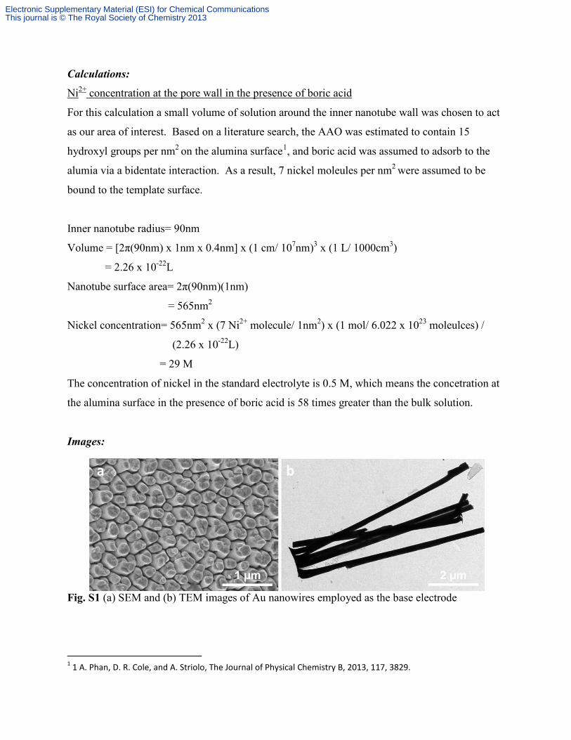
Calculations:
Ni2+ concentration at the pore wall in the presence of boric acid
For this calculation a small volume of solution around the inner nanotube wall was chosen to act
as our area of interest. Based on a literature search, the AAO was estimated to contain 15
hydroxyl groups per nm2 on the alumina surface1, and boric acid was assumed to adsorb to the
alumia via a bidentate interaction. As a result, 7 nickel moleules per nm2 were assumed to be
bound to the template surface.
Inner nanotube radius= 90nm
Volume = [2π(90nm) x 1nm x 0.4nm] x (1 cm/ 107nm)3 x (1 L/ 1000cm3)
= 2.26 x 10⁻²²L
Nanotube surface area= 2π(90nm)(1nm)
= 565nm2
Nickel concentration= 565nm2 x (7 Ni2+ molecule/ 1nm2) x (1 mol/ 6.022 x 10²³ moleulces) /
(2.26 x 10⁻²²L)
= 29 M
The concentration of nickel in the standard electrolyte is 0.5 M, which means the concetration at
the alumina surface in the presence of boric acid is 58 times greater than the bulk solution.
Images:
Fig. S1 (a) SEM and (b) TEM images of Au nanowires employed as the base electrode
1 1 A. Phan, D. R. Cole, and A. Striolo, The Journal of Physical Chemistry B, 2013, 117, 3829.
Electronic Supplementary Material (ESI) for Chemical CommunicationsThis journal is © The Royal Society of Chemistry 2013
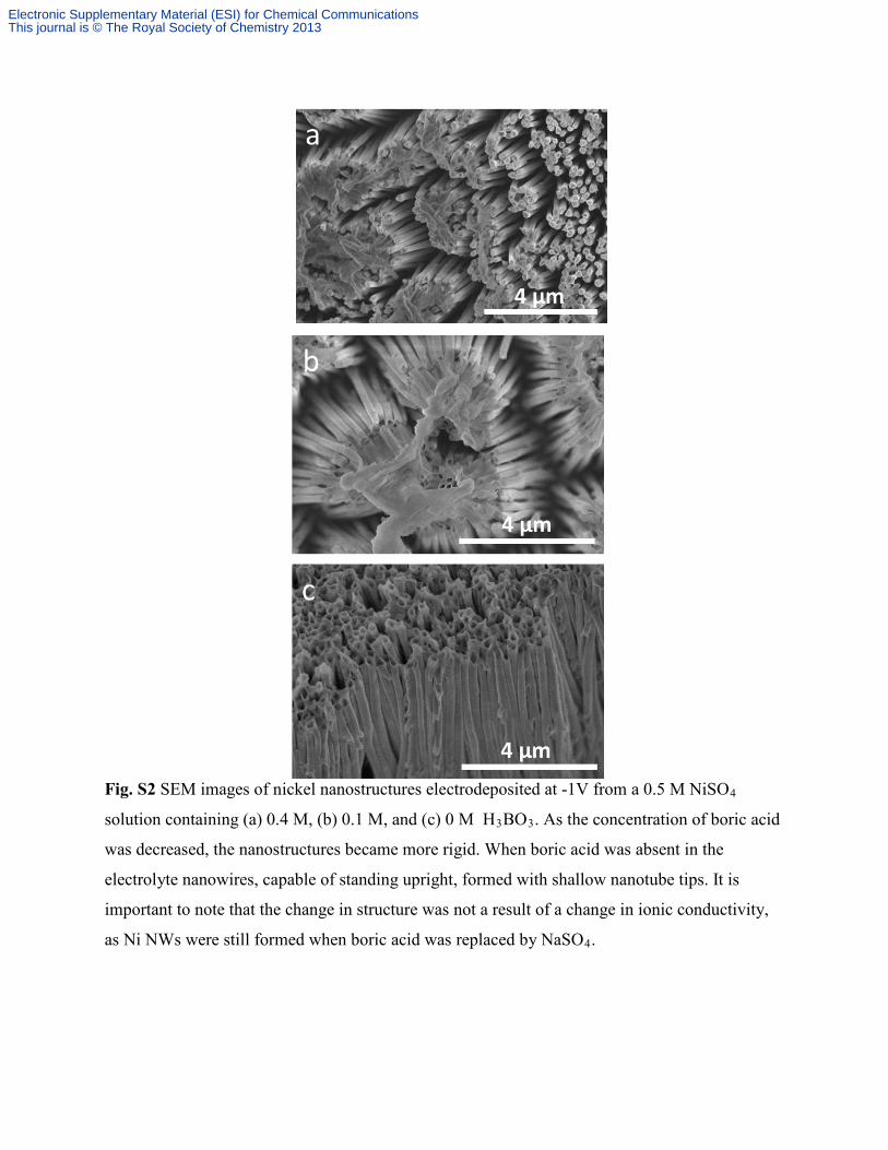
Fig. S2 SEM images of nickel nanostructures electrodeposited at -1V from a 0.5 M NiSO4
solution containing (a) 0.4 M, (b) 0.1 M, and (c) 0 M H3BO3. As the concentration of boric acid
was decreased, the nanostructures became more rigid. When boric acid was absent in the
electrolyte nanowires, capable of standing upright, formed with shallow nanotube tips. It is
important to note that the change in structure was not a result of a change in ionic conductivity,
as Ni NWs were still formed when boric acid was replaced by NaSO4.
Electronic Supplementary Material (ESI) for Chemical CommunicationsThis journal is © The Royal Society of Chemistry 2013
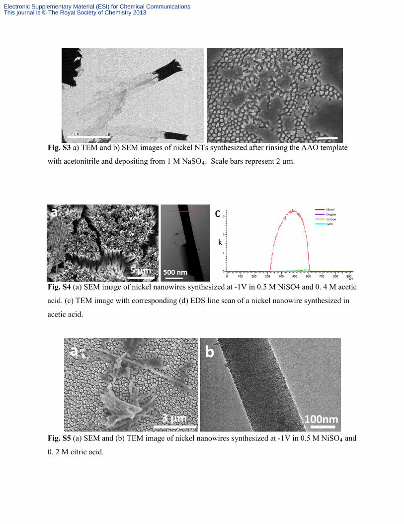
Fig. S3 a) TEM and b) SEM images of nickel NTs synthesized after rinsing the AAO template
with acetonitrile and depositing from 1 M NaSO4. Scale bars represent 2 µm.
Fig. S4 (a) SEM image of nickel nanowires synthesized at -1V in 0.5 M NiSO4 and 0. 4 M acetic
acid. (c) TEM image with corresponding (d) EDS line scan of a nickel nanowire synthesized in
acetic acid.
Fig. S5 (a) SEM and (b) TEM image of nickel nanowires synthesized at -1V in 0.5 M NiSO4 and
0. 2 M citric acid.
Electronic Supplementary Material (ESI) for Chemical CommunicationsThis journal is © The Royal Society of Chemistry 2013

Fig. S6 TEM images of nickel nanotubes synthesized at -1V in 0.5 M NiSO4, 0.4 M H3BO3 at pH (a) 1.8, (b) 3.1, and (c) 5.2.
Electronic Supplementary Material (ESI) for Chemical CommunicationsThis journal is © The Royal Society of Chemistry 2013

Fig. S7 Current density profile for the deposition of nickel.
Electronic Supplementary Material (ESI) for Chemical CommunicationsThis journal is © The Royal Society of Chemistry 2013

Fig. S8 TEM images of nickel nanotubes electrodeposited from a solution of 0.5 M NiSO4 and
0.4 M H3BO3 at (a) -0.4V, (b) -0.6V, and (c) -1V.
Electronic Supplementary Material (ESI) for Chemical CommunicationsThis journal is © The Royal Society of Chemistry 2013