
Electronic Packaging Technologies – from Bump Bonding to ... · • Functionally tested ASIC...
49
© Fraunhofer IZM [email protected] 1 University of Hamburg, 08.12.2017 Fraunhofer Institute for Reliability and Microintegration (IZM) Gustav-Meyer-Allee 25 13355 Berlin Germany Dipl.-Ing. Thomas Fritzsch Contact: [email protected] Electronic Packaging Technologies – from Bump Bonding to 3D Integration
Transcript of Electronic Packaging Technologies – from Bump Bonding to ... · • Functionally tested ASIC...
© Fraunhofer IZM [email protected]
1
University of Hamburg, 08.12.2017
Fraunhofer Institute for Reliability and Microintegration (IZM)
Gustav-Meyer-Allee 25
13355 Berlin
Germany
Dipl.-Ing. Thomas Fritzsch
Contact: [email protected]
Electronic Packaging Technologies –from Bump Bonding to 3D Integration

© Fraunhofer IZM [email protected]
2
University of Hamburg, 08.12.2017
Electronic Packaging
Telephone - Johann Philipp Reis1861
Wikipedia.de
Goal:Provide reliable interconnects and reliable systems fora specific application and under various conditions(temperature, moisture, vibration, radiation, dust)
Driving forces:Miniaturisation
Functionallity
Reliability
Cost
Packaging Level:Packaging at component level
Packaging at sub-assembly level
Packaging at system level
Packaging has four major functions:
Mechanical Connection
Electrical Connection (Signal and Power distribution)
Heat dissipation
Protection (mechanical, chemical, electromagnetic)
Smartphone 2013© David Hodson/www.ifixit.com

© Fraunhofer IZM [email protected]
3
University of Hamburg, 08.12.2017
Wire and Connector AssemblySub-Assembly IntegrationHousing
System - / Product Level
Electronic Packaging
Component-/ Wafer Level
Bumping and Interconnects
Redistribution Layer
Hermetic Caping / Sealing
Flip Chip Bonding
3D Chip Stacking
ReliabilityTemperature Cycle Test
Humidity Storage
Vibration / Drop Test
Power Cyling
PCB-/ Sub-Assembly Level
Wire Bonding
Soldering
Encapsulation / Molding
Flip Chip / SMD Assembly

© Fraunhofer IZM [email protected]
4
University of Hamburg, 08.12.2017
Outline
Fraunhofer IZM – The Electronic Packaging Institute
Wafer Level Packaging – Micro Bumping Technology
Bump Bonding and Interconnection Technologies for Hybrid
Pixel Radiation Detectors
3D Integration Technologies and Applications
5
© Fraunhofer IZM [email protected]
University of Hamburg, 08.12.2017
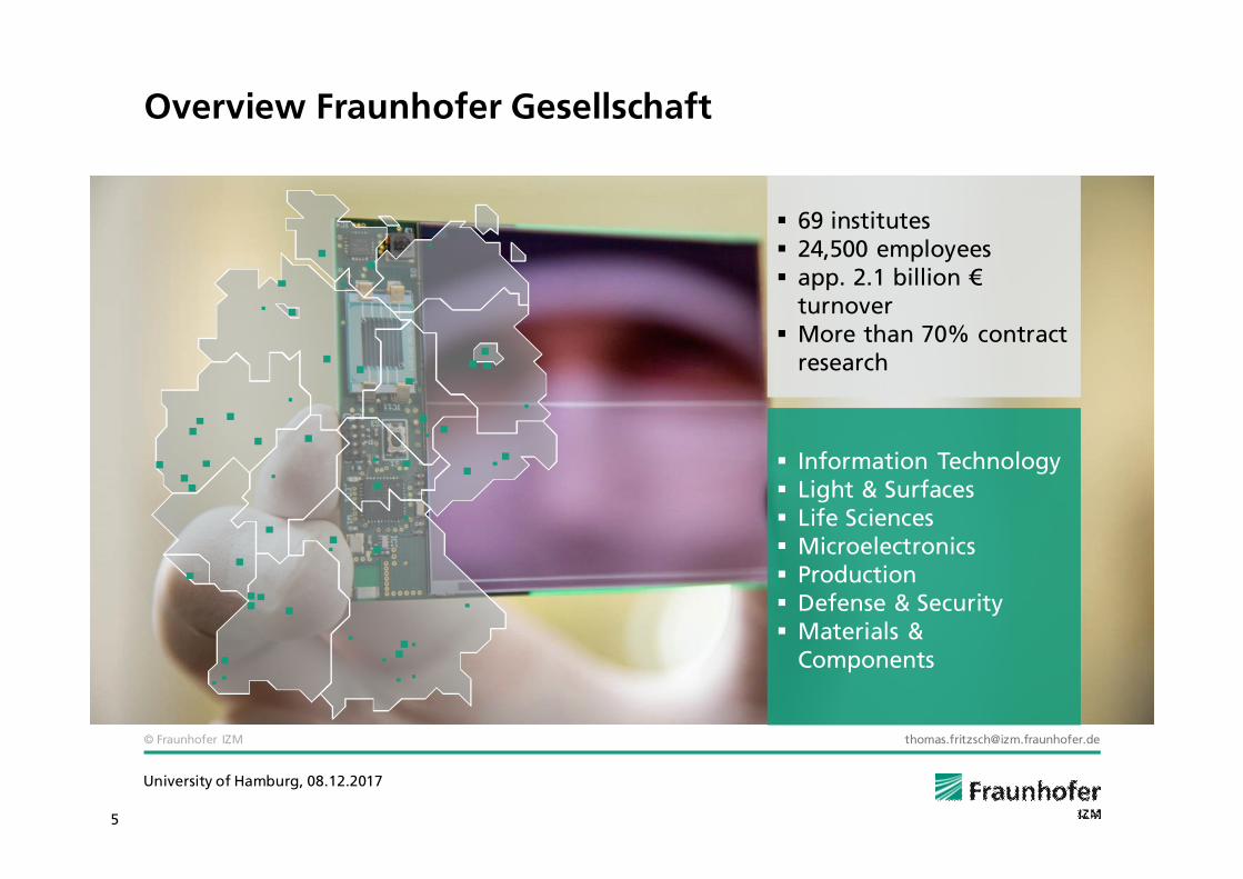
Overview Fraunhofer Gesellschaft
Information Technology Light & Surfaces Life SciencesMicroelectronicsProductionDefense & SecurityMaterials & Components
69 institutes24,500 employeesapp. 2.1 billion €turnoverMore than 70% contract research

© Fraunhofer IZM [email protected]
6
University of Hamburg, 08.12.2017
Fraunhofer Institute For Reliability and Microintegration - IZM
Material characterization Process evaluation Reliability testing Failure analysis Sample production Training courses
29.5 Mio. € turnover85 % contract research367 employees(235 full time, 132 students, PhD, trainee)
Figures 2016
DirectorProf. K.-D. Lang
BerlinDresden
Locations
Long-term contract with Technical University of BerlinResearch Center Microperipheric TechnologiesApprox. 90 additional staffJoint use of equipment, facilities and infrastructure
University Cooperation

7
© Fraunhofer IZM [email protected]
University of Hamburg, 08.12.2017
Fraunhofer IZMBringing Microelectronics into Application
Wafer Level Packaging
Printed Circuit Board Level Packaging Product Level
DesignASIC, components
Final Product

© Fraunhofer IZM [email protected]
8
University of Hamburg, 08.12.2017
Outline
Fraunhofer IZM – The Electronic Packaging Institute
Wafer Level Packaging – Micro Bumping Technology
Bump Bonding and Interconnection Technologies for Hybrid
Pixel Radiation Detectors
3D Integration Technologies and Applications

© Fraunhofer IZM [email protected]
9
University of Hamburg, 08.12.2017
Wafer Fabrication and Wafer Level Packaging (WLP)
Frontend - Wafer Fabrication
ASIC cross section
• ASIC fabrication on silicon wafer in sub-micron technology (180…22nm)
• Wafer size 150, 200, 300, (450) mm• Top pad metal aluminium (AlSi, AlSiCu,Cu)
developed for wire bonding• Functionally tested ASIC (KGD)
Structure size nm
©ZDNet
Backend - Wafer Level Packaging
Micro-Bumping25µm size
Thin Film MultilayerRedistribution (RDL)4…20µm width
Structure size µm
Adaption of ASICs tofurther assembly steps
Additional contactlayers (bumps, RDL, …)

© Fraunhofer IZM [email protected]
10
University of Hamburg, 08.12.2017
Fraunhofer IZM – ASSID DresdenFraunhofer IZM - Berlin
900 m² cleanroomWafer size: 200, 300mm
~ 800 m² cleanroomWafer size: 100, 150, 200, (300)mm
PVD Sputtering
CVD (Oxid / Barrier / Seed)
Polymer/ Resist application
Electrochemical depositionand Wet Etch
DRIE Si EtchThinning / Grinding
Wafer Bonding andDebonding
Chip BondingD2D, D2W
Dicing
Automatic OpticalWafer Inspection
CMP
Metrology
Wafer Level Packaging at Fraunhofer IZM
Lithography
© Fraunhofer IZM [email protected]
11
University of Hamburg, 08.12.2017
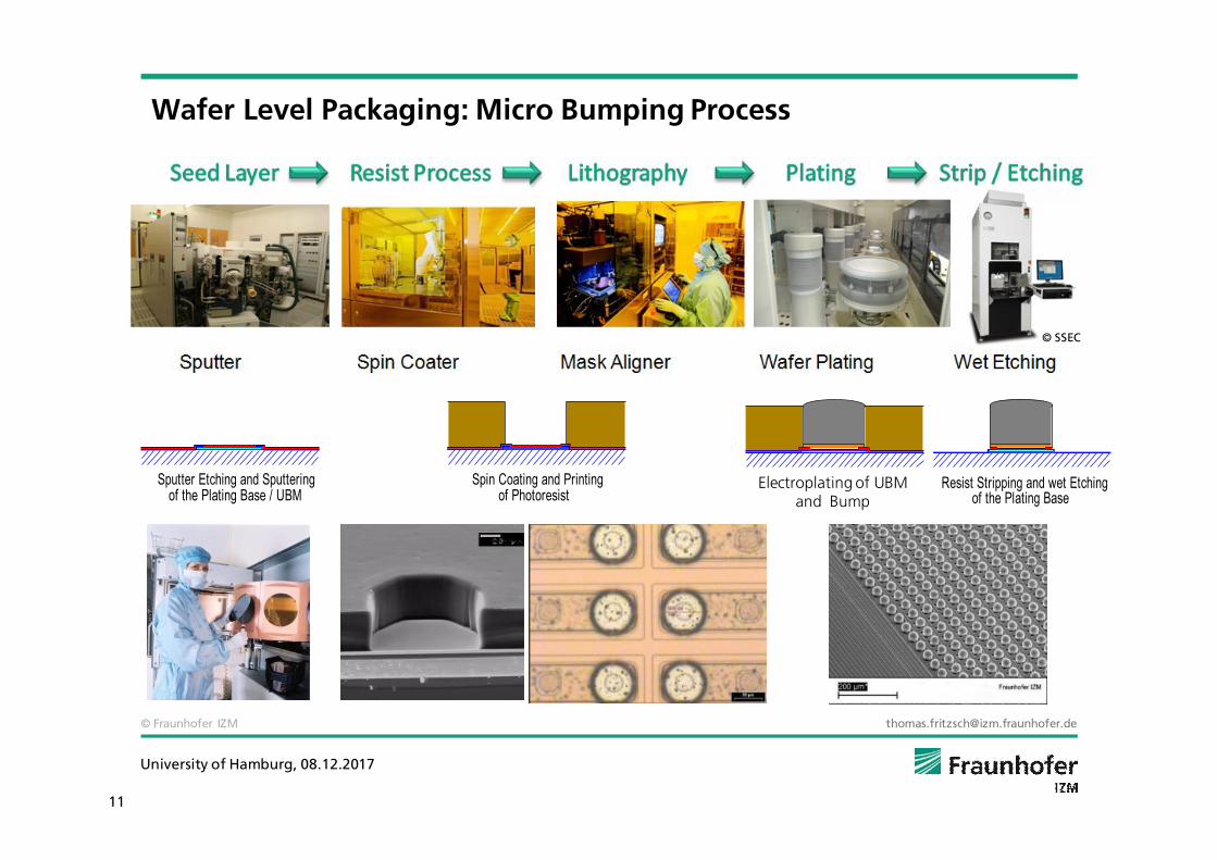
Wafer Level Packaging: Micro Bumping Process
Sputter Etching and Sputteringof the Plating Base / UBM
Spin Coating and Printingof Photoresist
Resist Stripping and wet Etchingof the Plating Base Electroplating of Cu and PbSnElectroplating of UBM
and Bump
© SSEC

© Fraunhofer IZM [email protected]
12
University of Hamburg, 08.12.2017
Physical Vapour Deposition (PVD) – Sputtering of Plating Base
Metal deposition: TiW, Ti, Cu, Au, Pt, NiCr, Al, AlSi, … (barrier + seed layer)
Layer thickness: 10…1000nm
Goals:
minimum layer stress
Diffusion barrier between contact pad and plating base
Plating base layer with low resistivity
Seed Layer Resist Lithography Plating Etching Inspection Dicing

© Fraunhofer IZM [email protected]
13
University of Hamburg, 08.12.2017
Resist Patterning by Mask Lithography
Resist deposition by spin-coating, spray-coating or dry film lamination
Resist thickness 5µm – 100µm
UV mask exposure & resist development
Goals:
Accurate wafer-mask alignment
Edge steepness/resist stability
Residue free via
Seed Layer Resist Lithography Plating Etching Inspection Dicing

© Fraunhofer IZM [email protected]
14
University of Hamburg, 08.12.2017
Electrochemical Deposition - Electroplating
A B
C
D E
F
G Rack PlaterA: Anode
B: Spray Tubes
C: Shielding
D: Wafer
E: Overflow
F: Immersion Heater
G: Level Switch
Metal deposition: Cu, Au, Ni, Sn, SnAg, In, Au/Ag
Layer thickness: 2…100µm
Goals:
Minimum layer stress
Homogenious layer thickness
Defect free deposition
Seed Layer Resist Lithography Plating Etching Inspection Dicing

© Fraunhofer IZM [email protected]
15
University of Hamburg, 08.12.2017
Wet Etching Process
Removal of resist layer by solvent solution
Removal of seed- and barrier layer by wet etching
Residueless removal of resist and plating base
Differential etch of TiW, Ti, Cu, Au, Cr
Tools:
Manual and automated wet etch processes available
Manual single wafer load and automated waferhandling process (C2C)
Seed Layer Resist Lithography Plating Etching Inspection Dicing
© SSEC
© Fraunhofer IZM [email protected]
16
University of Hamburg, 08.12.2017
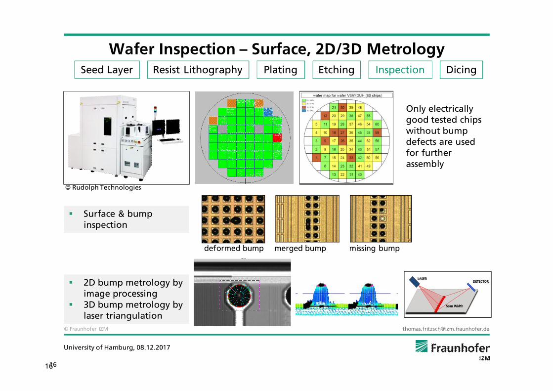
Wafer Inspection – Surface, 2D/3D Metrology
16
Only electrically good tested chips without bump defects are used for further assembly
merged bump missing bumpdeformed bump
2D bump metrology by image processing3D bump metrology by laser triangulation
Surface & bump inspection
Seed Layer Resist Lithography Plating Etching Inspection Dicing
© Rudolph Technologies

© Fraunhofer IZM [email protected]
17
University of Hamburg, 08.12.2017
Wafer Dicing
Dicing Technologies:Saw DicingLaser Dicing:
Full-CutStealth Dicing
Dicing by GrindingPlasma Dicing
Dicing Process:Mounting on dicing tapeDicing (saw, laser)Detaping and sorting
Source DISCO
Source Microworld Source DISCO
Seed Layer Resist Lithography Plating Etching Inspection Dicing

© Fraunhofer IZM [email protected]
18
University of Hamburg, 08.12.2017
Flip Chip Assembly
Flip Chip Assembly with Bonding Tools:
• High Accuracy Chip Pick and Place Process
• Interconnection by temperature and pressure: reflow soldering, thermo-compression bonding, thermosonic bonding
Chip 2 WaferChip 2 Chip
Chip with function Ai.e. ASIC
Chip withfunction Bi.e. sensor, MEMS

© Fraunhofer IZM [email protected]
19
University of Hamburg, 08.12.2017
SET FC150 Panasonic FCB3
High Accuracy Flip Chip Assembly – Bonder Tools
• Semi automatic flip chip bonder• Accuracy ± 1µm @ 3 Sigma• Bonding force up to 500N• C2C bonding• Substrate size up to 50 x 50 mm²• Capable for Adhesive-, TC- and Thermode
Bonding
• Full automatic flip chip bonder• Accuracy ± 3µm @ 3 Sigma• Bonding force up to 490N• C2C, C2W bonding• Substrate size up to 12“ wafer size• Capable for Adhesive-, TC- and TS
Bonding
© set-na.com © panasonicfa.com

© Fraunhofer IZM [email protected]
20
University of Hamburg, 08.12.2017
X-ray Inspection
Process:X-ray scanning of moduleAlignment between sensor and ROCMissing / Bridged BumpsParticles / residuesNo open bump connections detectable!
source: http://www.phoenix-xray.com/
Misalignedchip
particles Missing bumps/Bridged bumps
Xray source
DeviceUnderTest
Xray detector screen

© Fraunhofer IZM [email protected]
21
University of Hamburg, 08.12.2017
Outline
Fraunhofer IZM – The Electronic Packaging Institute
Wafer Level Packaging – Micro Bumping Technology
Bump Bonding and Interconnection Technologies for Hybrid
Pixel Radiation Detectors
3D Integration Technologies and Applications

© Fraunhofer IZM [email protected]
22
University of Hamburg, 08.12.2017
Readout Chip
Pixel Sensor Chip
Sensor Pixel
Communication, Data processing
Flip Chip Interconnection
Back Side Electrode
Setup:
Sensor chip
Readout chip
Function:
particle / photon
Hybrid Pixel Detectors

© Fraunhofer IZM [email protected]
23
University of Hamburg, 08.12.2017
Advantages:Separate development and optimization of sensor and readout chip
Variable use of different semiconductor sensor materials
SensorRadiation hardness
High detection efficiency
Fast signal response
High spectral and spatial resolution
Large detector array
Requirements
Readout ChipRadiation hardness
High readout speed
Low noise electronic
Low power consumption
Short connections to the sensor
Hybrid Pixel Detectors

© Fraunhofer IZM [email protected]
24
University of Hamburg, 08.12.2017
• Step 2: solder bump deposition on readout chip wafer
Flip Chip Bump Bonding
Packaging of Hybrid Pixel Detectors
• Step 3: Flip Chip Assembly of readout chip to sensor chip
• Step 1: UBM deposition on sensor wafer
© Fraunhofer IZM [email protected]
25
University of Hamburg, 08.12.2017
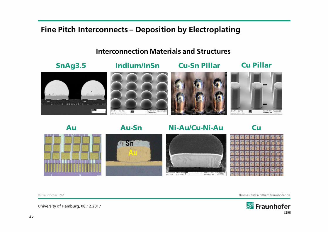
SnAg3.5 Indium/InSn Cu-Sn Pillar
Au-SnAu
Cu Pillar
Ni-Au/Cu-Ni-Au
Fine Pitch Interconnects – Deposition by Electroplating
Interconnection Materials and Structures
Cu

© Fraunhofer IZM [email protected]
26
University of Hamburg, 08.12.2017
SnAg Solder Bumping on 200mm Readout Chip (ROC) Wafer
TIMEPIX / MEDIPIX
Bump size: 25…30µmBump Pitch: 55µm (x, y)Chip Size: ~14 x 16 cm²Bump matrix: 256x257 (65792 per chip)Number of bumps: >7 Mio. (200mm)Application: Research, Industry
ATLAS FE-I4
Bump size: 25µmBump Pitch: 50µm (x, y1), 450µm (y2)Chip Size: ~20 x 20 cm²Bump matrix: 80 x 336 (26880 per chip)Number of bumps: >1.6 Mio. (200mm)Application: Research

© Fraunhofer IZM [email protected]
27
University of Hamburg, 08.12.2017
Hybrid Pixel Detectors for Particel Tracking and Xray Imaging
© CERN
Particle Tracking: LHC @ CERN
Hybrid pixel detector modules are the main building blocks of the inner tracking detector
© CERN
Courtesy of MEDIPIX Collaboration
X-ray Imaging for Synchrotrons
http://de.wikipedia.org/wiki/Röntgenbeugung
Hybrid pixel detector modules are usedfor x-ray imaging in photon-counting pixel detectors for synchrotrons and FEL

© Fraunhofer IZM [email protected]
28
University of Hamburg, 08.12.2017
CERN ATLAS IBL Pixel Tracking Detector UpgradeATLAS FE-I4B Modules for ATLAS Insertable B-Layer (IBL)
SnAg Bumping on 200mm Readout chip wafer, min. pitch 50µm
Assembly of 168 double and 112 single chip modules for ATLAS IBL
Readout Chip size 2x2 cm², module size 4x2 cm²
150µm thin chip ROC assembly
ATLAS FE-I4B double chip modul ATLAS IBL insertion(courtesy of Heinz Pernegger/CERN)
ATLAS Pixel Tracking Detector(InSpire/CERN)

© Fraunhofer IZM [email protected]
29
University of Hamburg, 08.12.2017
Silicon Pixel Detector Modules for the CMS Detector - Upgrade at LHC - CERNUpgrade Phase for the new 4 barrel layer CMS Silicon Pixel Detector
Fraunhofer IZM processed 316 modules for the 3rd layer (incl. spares)
SnAg Bumping of 26x 200mm Readout Chip wafers (6448 ROCs total)
Cu-UBM deposition on 130x 100mm sensor wafers
Flip Chip Assembly of 16 Readout Chips per module (5056 ROCs total)
Total module count: assembly of 316 modules
New 3rd layer with modules fabricated at IZM
Innermost part: silicon pixel tracking detector
CMS detector at LHC / CERN (© CMS/CERN)

© Fraunhofer IZM [email protected]
30
University of Hamburg, 08.12.2017
The European X-Ray Free-Electron Laser (XFEL) at DESY Hamburg
European XFEL, the largest and most powerful X-ray laser in the world, was officially inaugurated on September 1st, 2017
The European XFEL produces extremely bright and ultrashort light pulses. The facility will generate up to 27 000 pulses per second – 200 times more than other X-ray lasers.
With the help of specialized instruments, these X-rays enable completely new insights into the atomic details and extremely fast processes of the nanoworld.
Scientists will use these X-ray flashes to map the three-dimensional structure of biomolecules and other biological particles,
single snapshots of particles produced with the X-ray laser can be sewn together to create “molecular movies” to study the progress of biochemical and chemical reactions
[www.xfel.eu]
(© www.xfeal.eu)

© Fraunhofer IZM [email protected]
31
University of Hamburg, 08.12.2017
Pixel-Detector Modules for European X-Ray Free-Electron Laser (XFEL)
The European X-Ray Free Electron Laser (XFEL) will provide ultra-short, highly coherent X-ray pulses which will revolutionize scientific experiments in a variety of disciplines spanning physics, chemistry, materials science, and biology
European XFEL will provide very short x-ray pulses in a high repetition frequency with 27000 pulsesper second
Detection of molecule diffraction pattern with radiation hard X-ray cameras
Very fast and high dynamic range readout ASICs necessary because most experiments using particle injection mechanisms
Adaptive Gain Integrating Pixel Detector (AGIPD) Modules assembled at Fraunhofer IZM for European XFEL
http://de.wikipedia.org/wiki/Röntgenbeugung
www.xfel.eu
X-ray Diffractometry:

© Fraunhofer IZM [email protected]
32
University of Hamburg, 08.12.2017
Pixel-Detector Modules for European X-Ray Free-Electron Laser (XFEL)Adaptive Gain Integrating Pixel Detector (AGIPD) Modules assembled at Fraunhofer IZM for European XFEL
16-Chip Module with AGIPD Readout ASICS, module size 11x3 cm²
200 x 200 µm² pixel size, 65536 pixels per modules
1MPix X-ray camera consist of 16 modules positioned around the beam line center
Fabrication of AGIPD modules in cooperation with DESY
XFEL SPB-beamline withAGIPD Detector(SPB – Single particles, Clusters and Biomolecules)
Functional-Test ofAGIPD Detector-Three
Module Camera
© A.Allahgholi - CFEL© A.Allahgholi - CFEL

© Fraunhofer IZM [email protected]
33
University of Hamburg, 08.12.2017
Detectors with “high-Z” Sensors for Hard X-rays
D. Pennicard. Germanium pixel detector, 2013.
Materials:
Cadmium Telluride
Gallium Arsenide
Germanium
CdTe Sensor with Pixel metallizationGaAs Sensor with Pixel metallization
Requirements:
Bump Material adapted to GaAs and CdTe pad metallization
Maximum process and bonding temperaturebelow 120°C … 150°C (CdTe, Ge)
Low bonding pressure
Indium based solder bumps
© Fraunhofer IZM [email protected]
34
University of Hamburg, 08.12.2017
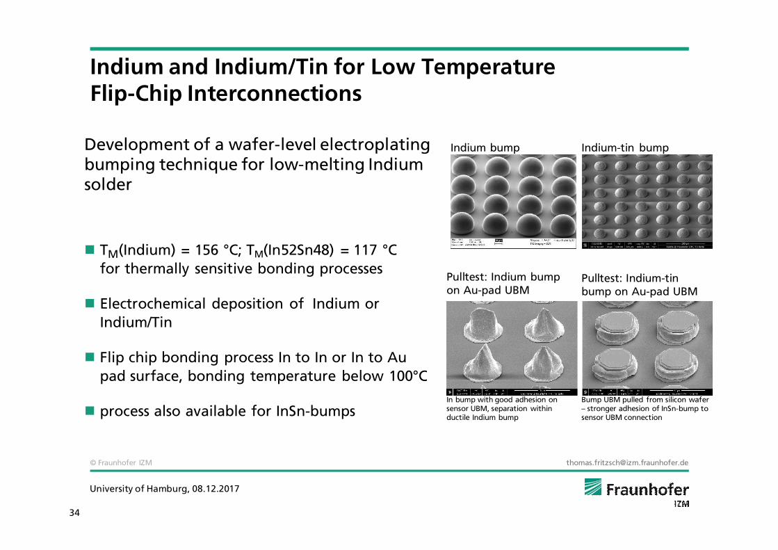
Development of a wafer-level electroplatingbumping technique for low-melting Indium solder
TM(Indium) = 156 °C; TM(In52Sn48) = 117 °Cfor thermally sensitive bonding processes
Electrochemical deposition of Indium orIndium/Tin
Flip chip bonding process In to In or In to Au pad surface, bonding temperature below 100°C
process also available for InSn-bumps
Indium and Indium/Tin for Low Temperature Flip-Chip Interconnections
Indium-tin bumpIndium bump
Pulltest: Indium bumpon Au-pad UBM
Pulltest: Indium-tinbump on Au-pad UBM
Bump UBM pulled from silicon wafer– stronger adhesion of InSn-bump tosensor UBM connection
In bump with good adhesion on sensor UBM, separation withinductile Indium bump

© Fraunhofer IZM [email protected]
35
University of Hamburg, 08.12.2017
Germanium X-ray detector using Indium bumping
2015: Ge Sensor HEXA Module

© Fraunhofer IZM [email protected]
36
University of Hamburg, 08.12.2017
Germanium X-ray detector using Indium bumping
spot of cosmic radiation with Ge HEXA Detector
M. Sarajilic, Medipix Meeting, Maastricht 18.05.2016

© Fraunhofer IZM [email protected]
37
University of Hamburg, 08.12.2017
Alternative Bonding Techniques for 3D Integration
Transient Liquid Phase (TLP) Bonding
Cu3Sn Intermetallics
Cu
CuSn
• ECD Cu and Cu-Sn pads
• High melting Cu3Sn IMC Ts = 700°C
• Bonding parameters: 220…280°C, 10…50MPa
• High planarity necessary
Metal-Metal DirectBonding
Cu, (Au, Ni)
Cu, (Au, Ni)
• ECD Cu pads (Au, Ni)
• Planarized surfaces, pre-conditioning
• Bonding parameters: 300°C…400°C, >100MPa, t= min…h, vacuum
Pillar bump bonding
• ECD Cu-pillar withsolder cap
• Short reflow process
• Use of underfiller forhigher reliability
• Use of different soldertypes for chip stacking
Higher Bonding and Application Temperature

© Fraunhofer IZM [email protected]
38
University of Hamburg, 08.12.2017
Development electro-plating baths for Ag/Au alloy deposition
Prozess flow similar to conventional Au Bumping
Skeleton formation due to simple dealloying by wet etching of Ag
Average pore sizes adjustable from 20 nm up to 500 nm
TC-Bonding with reduced bonding parameters possible,typ. 10 Mpa / 200°C / 300s
Sponge-like Au is fully compressible and able to compensate topography and inhomogeneities on chip and substrate
R&D: Nano-Porous Gold Bumps for Chip Interconnections

© Fraunhofer IZM [email protected]
39
University of Hamburg, 08.12.2017
Outline
Fraunhofer IZM – The Electronic Packaging Institute
Wafer Level Packaging – Micro Bumping Technology
Bump Bonding and Interconnection Technologies for Hybrid
Pixel Radiation Detectors
3D Integration Technologies and Applications

© Fraunhofer IZM [email protected]
40
University of Hamburg, 08.12.2017
2.5D/3D Integration Technology
Filled TSV (2…20µm Ø)for high density throughvia interconnects
Interposer applicationsHigh IO ASICs
Linered TSV (>20µm Ø)for moderate density through via interconnects
Low IO ASIC and sensors
TSV – Through Silicon Via
LETI

© Fraunhofer IZM [email protected]
41
University of Hamburg, 08.12.2017
Basic Technologies for TSV Formation
1.TSV siliconetchingDRIE BOSCH Process
2. TSV-InsulationTEOS, PE-CVD, SA-CVD,
3. Barrier-/Seed-LayerTi (TiW, TiN, Ta(N)) / Cu HI-PVD
4. Via fillingECD Cu bottomup filling
© DISCO
5. Si-Thinning / TSV-Reveal Backside
6. Frontside- /Backside RDLCu-Electroplating orAl-Sputtering

© Fraunhofer IZM [email protected]
42
University of Hamburg, 08.12.2017
IC1IC2
Interposer
Application: Silicon Interposer for High Bandwidth Module
Front: HD-side
Back: PCB-side(as seen in a mirror)
More than 200 modules delivered by IZM
Fabrication of silicon interposers with Cu TSVs and high density RDL at 200 mm Size: 20 x 21,7 mm2, Thickness: 100 m42,459 TSVs per DeviceCu-TSV density ~10,000/cm²
© Fraunhofer IZM [email protected]
43
University of Hamburg, 08.12.2017
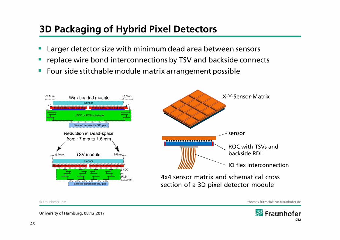
3D Packaging of Hybrid Pixel Detectors
Larger detector size with minimum dead area between sensors
replace wire bond interconnections by TSV and backside connects
Four side stitchable module matrix arrangement possible
4x4 sensor matrix and schematical cross section of a 3D pixel detector module
sensor
ROC with TSVs and backside RDL
IO flex interconnection
X-Y-Sensor-Matrix

© Fraunhofer IZM [email protected]
44
University of Hamburg, 08.12.2017
MEDIPIX3 TSV Development
RDL lines and pad metallisation
• TSV process from wafer backside• UBM on MEDIPIX wafer• Bumping of sensor wafer• Module hybridization• 2nd level assembly of LTCC/PCB substrate
Cu-filled TSV (x-ray left, cross cut right)
© Fraunhofer IZM [email protected]
45
University of Hamburg, 08.12.2017
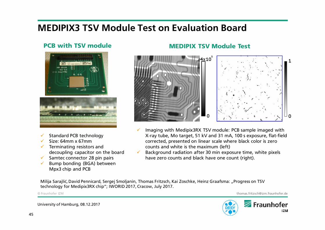
MEDIPIX3 TSV Module Test on Evaluation Board
PCB with TSV module
Standard PCB technologySize: 64mm x 67mmTerminating resistors anddecoupling capacitor on the boardSamtec connector 28 pin pairsBump bonding (BGA) betweenMpx3 chip and PCB
MEDIPIX TSV Module Test
Imaging with Medipix3RX TSV module: PCB sample imaged with X-ray tube, Mo target, 51 kV and 31 mA, 100 s exposure, flat-field corrected, presented on linear scale where black color is zero counts and white is the maximum (left)Background radiation after 30 min exposure time, white pixels have zero counts and black have one count (right).
Milija Sarajli , David Pennicard, Sergej Smoljanin, Thomas Fritzsch, Kai Zoschke, Heinz Graafsma: „Progress on TSV technology for Medipix3RX chip”; IWORID 2017, Cracow, July 2017.

© Fraunhofer IZM [email protected]
46
University of Hamburg, 08.12.2017
TSV Process for Ultra Fast Xray Pixel Matrix Chip
Process at IZM:
TSV-frontside process
Completely-filled Cu-TSV
Frontside and backside RDL
Fronside Solder Bumps/Pillars
Backside solderable Pad
Metallization
Hybridization to sensor
2nd level assembly to LTCC
ROC backside after TSV and backsideRDL process
UFXC32k Readout Chip developed by AGH Krakow, Poland
Prepared for TSV frontside option
Cross section of ROC-Sensor Module, with Cu filled TSV
TSV ROC

© Fraunhofer IZM [email protected]
47
University of Hamburg, 08.12.2017
TSV Process for Ultra Fast Xray Pixel Matrix Chip
The tests of a detector module:measurement of a total power consumption (1.7 W @ 200 MHz)
functionality verification of digital blocks in UFXC32k ICs
(registers and counters readout),
measurements of the effective offset spread from pixel to pixel
before and after trimming,
test with the charge injection circuit to verify the in-pixel analog
front-end operation,
test with X-ray radiation of different energy,
measurement of example radiograms.
Kai Zoschke et al. “Fabrication of 3D Hybrid Pixel Detector Modules Based on TSV Processing and Advanced Flip Chip Assembly of Thin Read Out Chips”, ECTC 2017, Lake Buena Vista, Florida, May 30 to June 2, 2017.

© Fraunhofer IZM [email protected]
48
University of Hamburg, 08.12.2017
Summary
Bump Bonding and Interconnection Technologies SnAg, In solder bump deposition and bump bondingUsed for Hybrid Pixel Detector Modules for Particletracking in High Energy Physics and X-ray imagingfor synchrotrons and FEL
3D Integration Technologies and Applications2.5D and 3D integration technology using TSVsInterposer and active die stacking3D packaging on R&D level for hybrid pixeldetectors available
Wafer Level Packaging – A Micro Integration Technology Adaption of IOs to further chip assembly steps and integration into electronical systemsBumping, RDL, TSV processes, Chip assembly

© Fraunhofer IZM [email protected]
49
University of Hamburg, 08.12.2017
Thank You For Your Attention
Fraunhofer Institute for Reliability and Microintegration (IZM)Gustav-Meyer-Allee 2513355 Berlin, GermanyContact: [email protected]


![[RecoPick] ZDNet 발표자료_20140703](https://static.fdocuments.net/doc/165x107/558bd10ed8b42ad9448b4657/recopick-zdnet-20140703.jpg)


![[ZDNet korea] 7th Cvision Daum tv](https://static.fdocuments.net/doc/165x107/547dc91e5806b5e55e8b45f3/zdnet-korea-7th-cvision-daum-tv.jpg)

![미래인터넷 서비스와 User-Centric Identity Management · 웹2.0 기반의신규서비스창출을위해서는프라이버시보호가필수적임[ZDNet, ‘06.12] 디지털ID보안연구팀](https://static.fdocuments.net/doc/165x107/60224485e5a7b5115b204768/eee-oee-user-centric-identity-20-eeeoeoeeoeoeoeeeeoeeezdnet.jpg)

