Electronic Engineering Laboratory IV
15
Lab No. 1 Lab Title CPU Instructions Semester 01 Session 2021/2022 Lab Duration 4 Hours (2 weeks) Electronic Engineering Laboratory IV BEJ40401 Instruction Sheet Faculty of Electric and Electronic Engineering
Transcript of Electronic Engineering Laboratory IV
Lab No. 1
Lab Title CPU Instructions
Semester 01
Session 2021/2022
Lab Duration 4 Hours (2 weeks)
Electronic Engineering Laboratory IV
BEJ40401
Instruction Sheet
Fa
cult
y o
f E
lect
ric
an
d E
lect
ron
ic E
ng
ine
eri
ng
Electronic Engineering Laboratory IV (BEJ40401)
Lab1: CPU Instructions ii
FKEE, Semester 01 Session 2021/2022
Table of Content
Table of Content 2
1.0 Outcomes 1
2.0 Guidelines 1
3.0 Pre-Lab (5%) 2
4.0 Lab instructions 2
Overview 2
5.0 Lab activity 1 (15%) 4
6.0 Lab activity 2 (15%) 6
7.0 Observations (15%) 9
8.0 Questions (15%) 10
9.0 References 10
10.0 Appendix 11
CPU Simulator Instruction Set 11
Electronic Engineering Laboratory IV (BEJ40401)
Lab1: CPU Instructions 1
FKEE, Semester 01 Session 2021/2022
1.0 Outcomes
After completing this module, the students should be able to:
1. Generate an appropriate basic CPU instruction on the CPU-OS simulator.
2. Perform the algorithm or program for computer architecture using CPU-OS simulator.
3. Adapt the current technology in computer architecture with morale and etiquette.
2.0 Guidelines
1. Lab group: should consist of two team members.
2. Pre-Lab: pre-lab questions should be answered before the lab session and should be attached with the lab report.
3. Lab Activities: all lab activities such as sample code, examples and lab assignments should be completed within the given times.
4. Demonstration: students should demonstrate the successful sample code, examples,
and lab assignments to the respective instructor. Verification only will be given upon completion of all lab activities and initialized by the instructor on the cover page.
5. Report Organization: report must be organized according to the given report template.
6. Report Submission: report must be submitted not later than one week upon
completion of the lab session.
Electronic Engineering Laboratory IV (BEJ40401)
Lab1: CPU Instructions 2
FKEE, Semester 01 Session 2021/2022
3.0 Pre-Lab (5%)
1. Explain the functions of the special CPU register: Program Counter (PC), Status Register (SR), and Stack Pointer (SP) register.
2. What kinds of CPU instructions are used to store values on top of the stack?
3. What is subroutine? What is the function of a subroutine?
4.0 Lab instructions
Overview
(2 marks)
(1 mark)
(2 marks)
The programming model of computer architecture defines those low-level architectural
components, which include the following
▪ CPU instruction set
▪ CPU registers
▪ Different ways of addressing instructions and data in instructions
It also defines the interaction between the above components. It is a low-level programming
model that makes programmed computations possible.
Next is some basic information on the simulator, which should enable the students to use the
simulator. The simulator for this lab is running on the MS Windows operating systems.
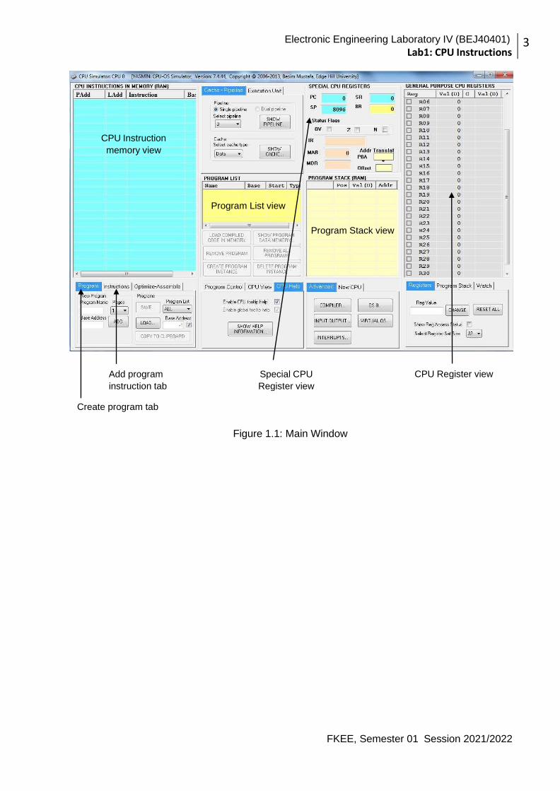
The main window is composed of several views, which represent different functional parts of the
simulated processor. These are shown in Figure 1.1 and are consist of
▪ CPU Instruction Memory
▪ Special CPU Registers
▪ General Purpose CPU Registers
▪ Program Stack
▪ Program Creation and Running Features
Electronic Engineering Laboratory IV (BEJ40401)
Lab1: CPU Instructions 3
FKEE, Semester 01 Session 2021/2022
Create program tab
Figure 1.1: Main Window
CPU Instruction
memory view
Program List view
Program Stack view
Add program
instruction tab
Special CPU
Register view
CPU Register view
Electronic Engineering Laboratory IV (BEJ40401)
Lab1: CPU Instructions 4
FKEE, Semester 01 Session 2021/2022
5.0 Lab activity 1 (15%)
First, we need to place some instructions in the Instruction Memory View, representing the
RAM in the real machine, before executing any instructions.
1. In the Program tab, first, enter a Program Name, and then enter a Base Address (this
can be any number, but for this exercise use 100).
2. Click on the ADD button. A new program name will be entered in the Program List view.
Now, we are ready to enter instructions into the CPU simulator. We do this by clicking on the
ADD NEW button in the Instructions tab. This will display the Instruction: CPU0 window. We
use this window to select and enter the CPU instructions. The appendix lists some of the
instructions this simulator uses and also gives examples of their usage.
3. Create an instruction, which moves number 5 to register R00. Execute the above instruction
(to do this, simply double click on it in the Instruction Memory View). Observe the result in
the CPU Registers View.
4. Create an instruction, which moves number 8 to register R01. Execute it (double click on the
instruction). Observe the contents of R00 and R01.
5. Create an instruction, which adds the contents of R00 and R01. Execute it, and observe
which register the result is put in.
6. Create an instruction, which pushes the above result to the top of the hardware stack, and
then execute it.
7. Create an instruction to push number -2 on top of the stack and execute it. Observe the
value in Program Stack.
8. Observe the value in the SP register (Special CPU Register view). Whenever we push a
value on Program Stack, the SP register is updated.
9. Create an instruction to compare the values in registers R00 and R01. Execute it, and
observe the value in SR (Special CPU Registers view).
10. Observe the status of the OV/Z/N parts of the status register. Which boxes are checked and
which are not? What do they indicate?
11. Create an instruction to unconditionally jump to the first instruction. Execute it, and observe
the value in the PC register. This is the address of the next instruction to be executed. Make
a note of which instruction it is pointing to?
12. Observe the values in the PAdd and LAdd columns. What do these values indicate? Are
they different (Hint: Check out Base Address value)?
13. Create an instruction to pop the value on top of the Program Stack into register R02.
Execute it, and observe the value in the SP register.
Electronic Engineering Laboratory IV (BEJ40401)
Lab1: CPU Instructions 5
FKEE, Semester 01 Session 2021/2022
14. Create an instruction to pop the value on top of the Program Stack into register R03.
Execute it, and observe the value in the SP register.
15. Execute the last instruction again. What happened? Explain.
16. Create a compare instruction, which compares values in registers R04 and R05.
17. Manually insert two equal values in registers R04 and R05. Execute the compare instruction.
Which of the status flags OV/Z/N is set? Why?
18. Manually insert a value in register R05 greater than that in register R04. Execute the
compare instruction. Which of the status flags OV/Z/N is set? Why?
19. Manually insert a value in register R04 greater than that in register R05. Execute the
compare instruction. Which of the status flags OV/Z/N is set? Why?
20. Create an instruction, which will jump to the first instruction if the values in register R04 and
R05 are equal. Test this instruction by manually putting equal values in register R04 and R05,
then first executing the compare instruction followed by executing the jump instruction.
21. Create an instruction that subtracts the content in R04 and R05 if the condition in the
previous instructions is not met. Execute the instruction that compares the content of R04
and R05. Observe the register that stores the result.
22. Save the instructions in the Instruction Memory View in a file by clicking on the SAVE
button.
Electronic Engineering Laboratory IV (BEJ40401)
Lab1: CPU Instructions 6
FKEE, Semester 01 Session 2021/2022
MOV
L0:
ADD
CMP
JNE
HLT
#0, R01
#1, R01
#5, R01
$L0
6.0 Lab activity 2 (15%)
In this assignment, the students will be familiar with direct and indirect addressing modes of
accessing data in memory. The students also learn about subroutine, call and return from a
subroutine, to create an iterative loop of instruction.
First, you need to place some instruction in the Instruction Memory View, representing the
RAM in the real machine, before executing any instructions.
1. In the Appendix (at the end of this document), locate the instruction, which is used to
store one byte of data in a memory location. Use it to store number 65 in address location 20
using direct addressing mode (all numbers are in decimal).
2. Create an instruction to move decimal number 22 to register. Execute this instruction and
verify the result in R01
3. Create an instruction to store decimal number 51 in memory location the address of which is
currently stored in register R01. This is an example of indirect addressing. Note the use of
“@” prefix next to R01 in this case.
4. Observe data memory locations 20 and 22.
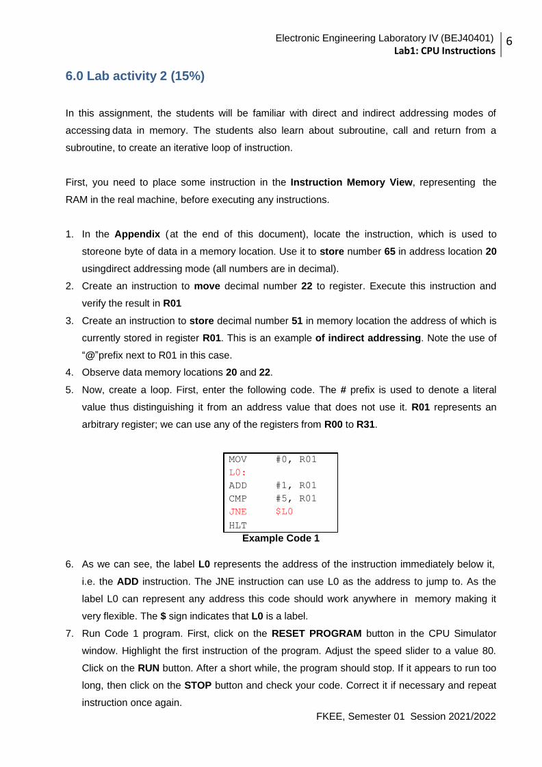
5. Now, create a loop. First, enter the following code. The # prefix is used to denote a literal
value thus distinguishing it from an address value that does not use it. R01 represents an
arbitrary register; we can use any of the registers from R00 to R31.
Example Code 1
6. As we can see, the label L0 represents the address of the instruction immediately below it,
i.e. the ADD instruction. The JNE instruction can use L0 as the address to jump to. As the
label L0 can represent any address this code should work anywhere in memory making it
very flexible. The $ sign indicates that L0 is a label.
7. Run Code 1 program. First, click on the RESET PROGRAM button in the CPU Simulator
window. Highlight the first instruction of the program. Adjust the speed slider to a value 80.
Click on the RUN button. After a short while, the program should stop. If it appears to run too
long, then click on the STOP button and check your code. Correct it if necessary and repeat
instruction once again.
Electronic Engineering Laboratory IV (BEJ40401)
Lab1: CPU Instructions 7
FKEE, Semester 01 Session 2021/2022
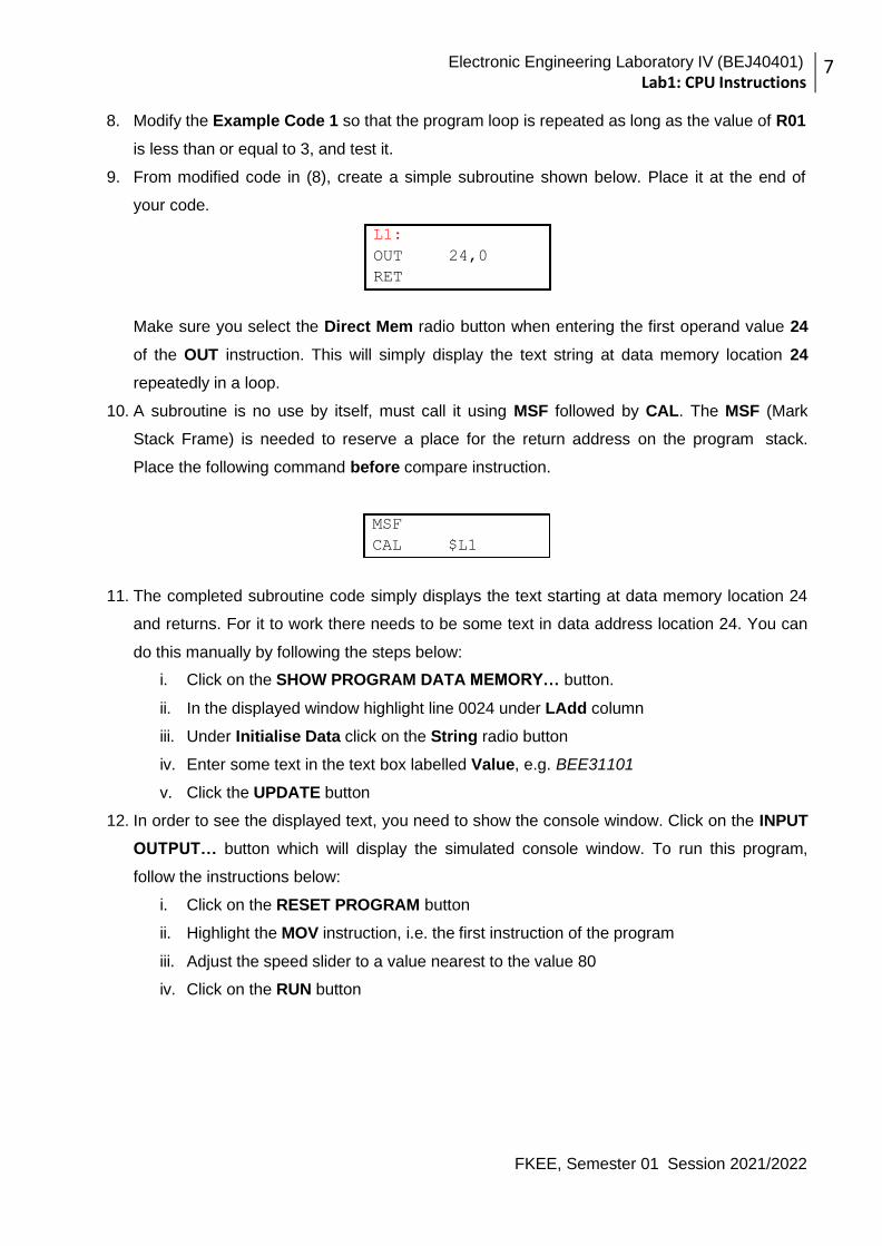
MSF
CAL $L1
8. Modify the Example Code 1 so that the program loop is repeated as long as the value of R01
is less than or equal to 3, and test it.
9. From modified code in (8), create a simple subroutine shown below. Place it at the end of
your code.
Make sure you select the Direct Mem radio button when entering the first operand value 24
of the OUT instruction. This will simply display the text string at data memory location 24
repeatedly in a loop.
10. A subroutine is no use by itself, must call it using MSF followed by CAL. The MSF (Mark
Stack Frame) is needed to reserve a place for the return address on the program stack.
Place the following command before compare instruction.
11. The completed subroutine code simply displays the text starting at data memory location 24
and returns. For it to work there needs to be some text in data address location 24. You can
do this manually by following the steps below:
i. Click on the SHOW PROGRAM DATA MEMORY… button.
ii. In the displayed window highlight line 0024 under LAdd column
iii. Under Initialise Data click on the String radio button
iv. Enter some text in the text box labelled Value, e.g. BEE31101
v. Click the UPDATE button
12. In order to see the displayed text, you need to show the console window. Click on the INPUT
OUTPUT… button which will display the simulated console window. To run this program,
follow the instructions below:
i. Click on the RESET PROGRAM button
ii. Highlight the MOV instruction, i.e. the first instruction of the program
iii. Adjust the speed slider to a value nearest to the value 80
iv. Click on the RUN button
L1:
OUT
RET
24,0
Electronic Engineering Laboratory IV (BEJ40401)
Lab1: CPU Instructions 8
FKEE, Semester 01 Session 2021/2022
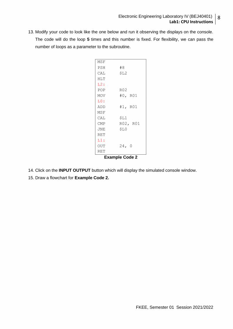
13. Modify your code to look like the one below and run it observing the displays on the console.
The code will do the loop 5 times and this number is fixed. For flexibility, we can pass the
number of loops as a parameter to the subroutine.
MSF
PSH
#8
CAL $L2
HLT
L2:
POP R02
MOV #0, R01
L0:
ADD #1, R01
MSF
CAL $L1
CMP R02, R01
JNE $L0
RET
L1:
OUT 24, 0
RET
Example Code 2
14. Click on the INPUT OUTPUT button which will display the simulated console window.
15. Draw a flowchart for Example Code 2.
Electronic Engineering Laboratory IV (BEJ40401)
Lab1: CPU Instructions 9
FKEE, Semester 01 Session 2021/2022
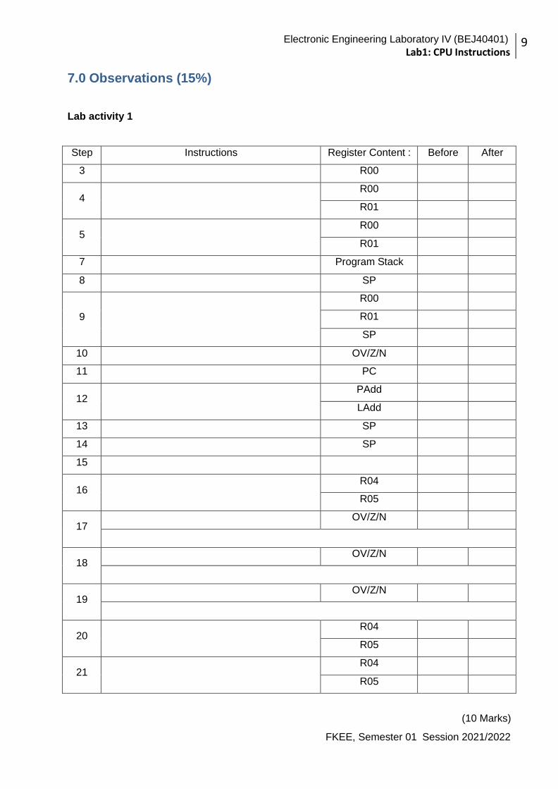
7.0 Observations (15%)
Lab activity 1
Step Instructions Register Content : Before After
3 R00
4 R00
R01
5 R00
R01
7 Program Stack
8 SP
9
R00
R01
SP
10 OV/Z/N
11 PC
12 PAdd
LAdd
13 SP
14 SP
15
16 R04
R05
17 OV/Z/N
18 OV/Z/N
19 OV/Z/N
20 R04
R05
21 R04
R05
(10 Marks)
Electronic Engineering Laboratory IV (BEJ40401)
Lab1: CPU Instructions 10
FKEE, Semester 01 Session 2021/2022
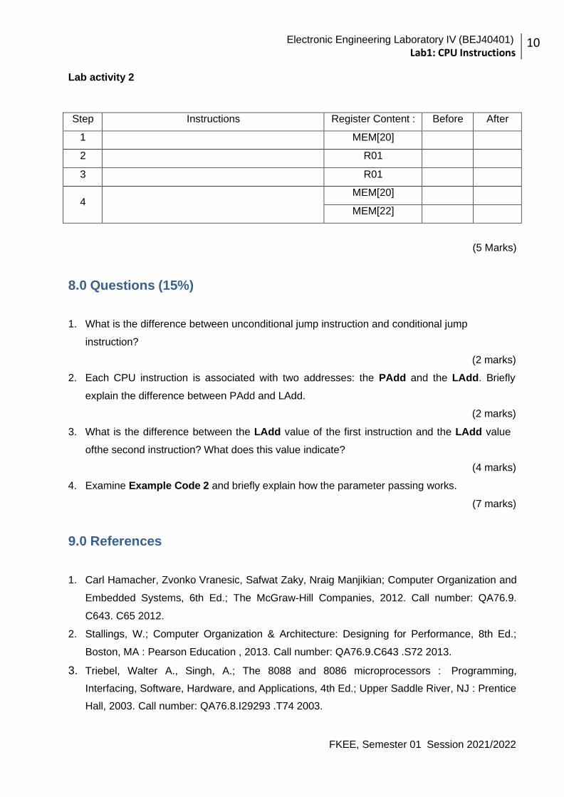
Lab activity 2
Step Instructions Register Content : Before After
1 MEM[20]
2 R01
3 R01
4 MEM[20]
MEM[22]
(5 Marks)
8.0 Questions (15%)
1. What is the difference between unconditional jump instruction and conditional jump
instruction?
(2 marks)
2. Each CPU instruction is associated with two addresses: the PAdd and the LAdd. Briefly
explain the difference between PAdd and LAdd.
(2 marks)
3. What is the difference between the LAdd value of the first instruction and the LAdd value
of the second instruction? What does this value indicate?
4. Examine Example Code 2 and briefly explain how the parameter passing works.
(4 marks)
(7 marks)
9.0 References
1. Carl Hamacher, Zvonko Vranesic, Safwat Zaky, Nraig Manjikian; Computer Organization and
Embedded Systems, 6th Ed.; The McGraw-Hill Companies, 2012. Call number: QA76.9.
C643. C65 2012.
2. Stallings, W.; Computer Organization & Architecture: Designing for Performance, 8th Ed.;
Boston, MA : Pearson Education , 2013. Call number: QA76.9.C643 .S72 2013.
3. Triebel, Walter A., Singh, A.; The 8088 and 8086 microprocessors : Programming,
Interfacing, Software, Hardware, and Applications, 4th Ed.; Upper Saddle River, NJ : Prentice
Hall, 2003. Call number: QA76.8.I29293 .T74 2003.
Electronic Engineering Laboratory IV (BEJ40401)
Lab1: CPU Instructions 11
FKEE, Semester 01 Session 2021/2022
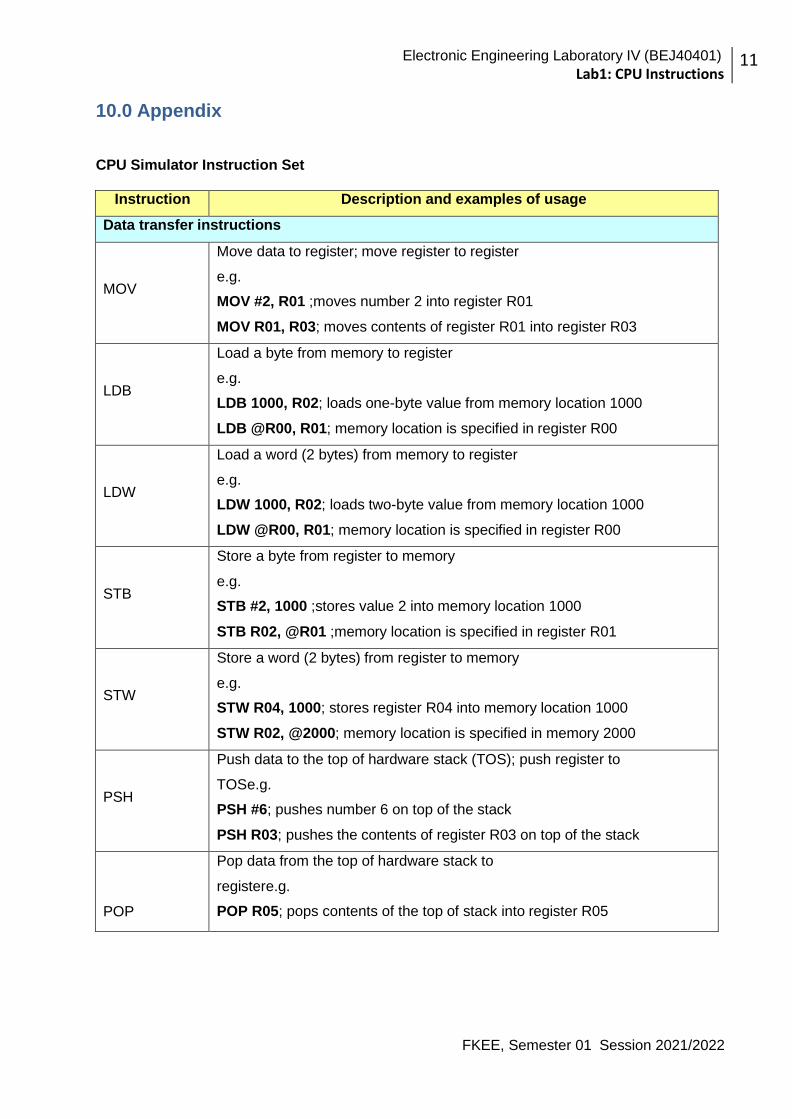
10.0 Appendix
CPU Simulator Instruction Set
Instruction Description and examples of usage
Data transfer instructions
MOV
Move data to register; move register to register
e.g.
MOV #2, R01 ;moves number 2 into register R01
MOV R01, R03; moves contents of register R01 into register R03
LDB
Load a byte from memory to register
e.g.
LDB 1000, R02; loads one-byte value from memory location 1000
LDB @R00, R01; memory location is specified in register R00
LDW
Load a word (2 bytes) from memory to register
e.g.
LDW 1000, R02; loads two-byte value from memory location 1000
LDW @R00, R01; memory location is specified in register R00
STB
Store a byte from register to memory
e.g.
STB #2, 1000 ;stores value 2 into memory location 1000
STB R02, @R01 ;memory location is specified in register R01
STW
Store a word (2 bytes) from register to memory
e.g.
STW R04, 1000; stores register R04 into memory location 1000
STW R02, @2000; memory location is specified in memory 2000
PSH
Push data to the top of hardware stack (TOS); push register to
TOS e.g.
PSH #6; pushes number 6 on top of the stack
PSH R03; pushes the contents of register R03 on top of the stack
POP
Pop data from the top of hardware stack to
register e.g.
POP R05; pops contents of the top of stack into register R05
Electronic Engineering Laboratory IV (BEJ40401)
Lab1: CPU Instructions 12
FKEE, Semester 01 Session 2021/2022
Arithmetic instructions
ADD
Add number to register; add register to register
e.g.
ADD #3, R02; adds number 3 to contents of register R02 and stores the
result in register R02.
ADD R00, R01; adds contents of register R00 to contents of register R01
and stores the result in register R01.
SUB Subtract number from register; subtract register from register.
MUL Multiply number with register; multiply register with register.
DIV Divide number with register; divide register with register.
Control transfer instructions
JMP
Jump to instruction address unconditionally
e.g.
JMP 100; unconditionally jumps to address location 100.
JLT
Jump to instruction address if less than (after the last
comparison) e.g.
JLT 120; jumps to address location 120 if the previous comparison
instruction result indicates that CMP operand 2 is less than CMP operand 1
(i.e. the N status flag is set). Also, see CMP instruction.
JGT
Jump to instruction address if greater than (after the last
comparison) e.g.
JGT 25; jumps to address location 25 if the previous comparison instruction
result indicates that CMP operand 2 is greater than CMP operand 1 (i.e.
flags Z and N not set). Also, see CMP instruction.
JEQ
Jump to instruction address if equal (after the last
comparison) e.g.
JEQ 1000; jumps to address location 1000 if the previous comparison
instruction result indicates that the two CMP operands are equal (i.e. the Z
status flag is set). Also, see CMP instruction.
JNE
Jump to instruction address if not equal (after the last
comparison) e.g.
JNE 220; jumps to address location 220 if the previous comparison
instruction result indicates that CMP operand 2 is less than CMP operand 1
(i.e. the N status flag is set). Also, see CMP instruction.
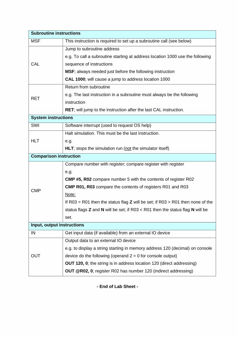
Subroutine instructions
MSF This instruction is required to set up a subroutine call (see below)
CAL
Jump to subroutine address
e.g. To call a subroutine starting at address location 1000 use the following
sequence of instructions
MSF; always needed just before the following instruction
CAL 1000; will cause a jump to address location 1000
RET
Return from subroutine
e.g. The last instruction in a subroutine must always be the following
instruction
RET; will jump to the instruction after the last CAL instruction.
System instructions
SWI Software interrupt (used to request OS help)
HLT
Halt simulation. This must be the last instruction.
e.g.
HLT; stops the simulation run (not the simulator itself)
Comparison instruction
CMP
Compare number with register; compare register with register
e.g.
CMP #5, R02 compare number 5 with the contents of register R02
CMP R01, R03 compare the contents of registers R01 and R03
Note:
If R03 = R01 then the status flag Z will be set; if R03 > R01 then none of the
status flags Z and N will be set; if R03 < R01 then the status flag N will be
set.
Input, output instructions
IN Get input data (if available) from an external IO device
OUT
Output data to an external IO device
e.g. to display a string starting in memory address 120 (decimal) on console
device do the following (operand 2 = 0 for console output)
OUT 120, 0; the string is in address location 120 (direct addressing)
OUT @R02, 0; register R02 has number 120 (indirect addressing)
- End of Lab Sheet -