Electron Microscopy - Wikis introduction to em_01.pdf · TEM dark field image g=(200)dyn HRTEM zone...
48
Electron Microscopy An Introduction MSE-621 2013 1 Electron Microscopy MSE-621 2013 1. Introduction, types of microscopes, some examples 2. Electron guns, Electron optics 3. SEM, interaction volume, contrasts 4. Electron diffraction, X-ray diffraction 5. TEM, contrast, image formation 2
Transcript of Electron Microscopy - Wikis introduction to em_01.pdf · TEM dark field image g=(200)dyn HRTEM zone...

Electron Microscopy
An Introduction
MSE-621 2013 1
Electron Microscopy
MSE-621 2013
1. Introduction, types of microscopes, some examples
2. Electron guns, Electron optics3. SEM, interaction volume,
contrasts4. Electron diffraction, X-ray
diffraction5. TEM, contrast, image formation
2

Microscopes…
http://www.ucmp.berkeley.edu/history/hooke.html
1665
2007
MSE-621 2013 3
Optical Microscopy
• Antique: first convex lenses• XII-XIII century: magnifying
power of convex lenses: magnifying glass, looking glasses
• 1590: Janssen, first comound microscope
• 1609 Galilei: occhiolino• 1665 Hooke: first image of
biological cell• 1801 Young: wave character of
light• 1872 (~) Abbe: resolution limit
linked to the wave length of the illuminating wave
MSE-621 2013 4

magnification
• Ratio between real size of an object and its apparent size on the image (paper, screen, eye)
MSE-621 2013 5
Which magnification…?
Who is lying ? The scale bar or the indicted magnification……?
Measure the size of a grain on the screen and calculate the magnification !
MSE-621 2013 6

resolution
MSE-621 2013 7
Why electrons…?
MSE-621 2013 8

Homework
How many electrons are at the same time in the column of a TEM…?
300keVL = 1.5 m
Beam current 1nA
MSE-621 2013 9
History
1897: J.J. Thomson: predicts the existence of electrons
1923: De Broglie: concept of wavelength associated to particles, confirmation by Young’s experiment
1927: Busch: focalisation low for magnetic fields, Davisson, Gremer, Thomson: electron diffraction
1931: Ruska, Knoll: first images by electron microscope
MSE-621 2013 10

History
FEI Titan2009
Siemens 1939
MSE-621 2013 11
Comparison of different microscopes
MSE-621 2013 12

Depth of field: photons and SEM
LM
~10-20°
SEM
~10-3 rad
10mm
1mm
100µm
10µm
1µm
0.1µm
10µm 1µm 100nm 10nm
10 102 103 104
1nm
105
SEMLM
=500nm
10mrad
1mrad
0.1mrad
Résolution
Pro
fond
eur
de c
ham
p h
Grandissement (grossissement) G
LM=0.5m
dept
h of
fiel
d h
resolution
magnification M
MSE-621 2013 13
Types of electron microscopes
TransmissionElectron Microscope
ScanningElectron Microscope
Slide ProjectorTV
What you see is what the
detector sees !!!
Scanning beam
MSE-621 2013 14

15
Types of microscopes
SEM• 0.3-30keV• Inelastic scattering: surface
information: topography• Chemical composition (EDX)• Pseudo-elastic (back-)
scattering: Compositional information (diffraction, EBSD)
• TEM• 60-300keV (up to 3 MeV)• “Projection” of the THIN
sample• Elastic scattering dominant:
Diffraction and diffraction contrast
• Interference between transmitted and diffracted beams: high-resolution (atomic resolution)
• Inelastic scattering: chemical composition (EDX)
MSE-621 2013
SEM, signals
X-rayselasticinelastic
Backscattered electrons
e-beam
Secondaryelectrons
photons Auger electrons
IR,UV,vis.
Absorbed current, EBIC
• Secondary electrons(~0-30eV), SE
• Backscattered electrons(~eVo), BSE
• Auger electrons
• Photons: visible, UV, IR,X-rays
• Phonons, Heating
• Absorbtion of incidentelectrons (EBIC-Current)
MSE-621 2013 16

Some typical SEM
At CIME:Zeiss NVision40
(FIB)
Zeiss UltraHR-SEM
Resolution
1.0 nm @ 15 kV, 1.7 nm @ 1 kV, 4.0 nm @ 0.1 kV
Magnification12 - 900,000x in SE mode Acceleration Voltage0.02 - 30 kV
Probe Current4 pA - 10 nA
Standard Detectors:EsB Detector with filtering gridHigh efficiency In-lens SE DetectorEverhart-Thornley Secondary Electron Detector
MSE-621 2013 17
SEM low kV imaging
No specimen preparation needed:Low kV imaging of non-conducting, low density samples
FEI MagellanOperator: Ingo GestmannSamples: Marco Cantoni
Al2O3 Nano-crystals
MSE-621 2013 18

Interaction e – matter in a TEM
MSE-621 2013 19
Signals from a thin sample
Specimen
Inc
ide
nt b
ea
m
Auger electrons
Backscattered electronsBSE
secondary electronsSE Characteristic
X-rays
visible light
“absorbed” electrons electron-hole pairs
elastically scatteredelectrons
dire
ct
be
am
inelasticallyscattered electrons
BremsstrahlungX-rays
1-100 nm
MSE-621 2013 20

Some “typical” TEMs
EPFL: Philips CM300
Japan: HITACHI H-1500
1’300’000V !!!
300’000V
resolution < 1.7Å
MSE-621 2013 21
22
Some “numbers”
• “Speed”of a 300keV electron: 76% oflight-speed
• Wavelength of a 300’000V beam:0.0197 Å~2pm (0.002nm)
• Image resolution: ~1.7Å• Typical scattering
angles: 10-3 rad
Pb
Mg/Nb
MSE-621 2013
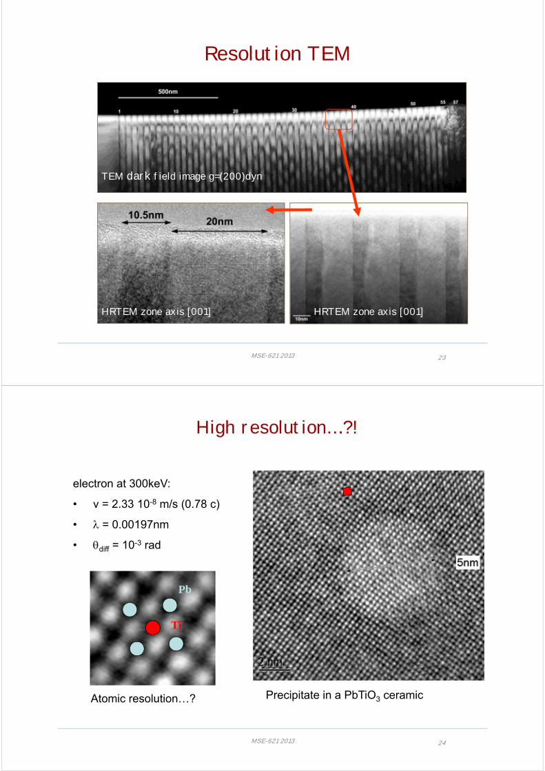
Resolution TEM
TEM dark field image g=(200)dyn
HRTEM zone axis [001] HRTEM zone axis [001]
MSE-621 2013 23
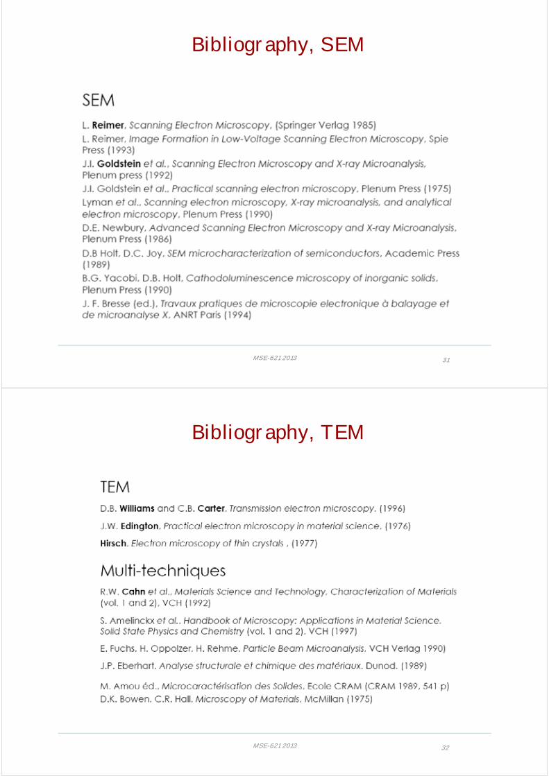
High resolution….?!
electron at 300keV:
• v = 2.33 10-8 m/s (0.78 c)
• = 0.00197nm
• diff = 10-3 rad
Precipitate in a PbTiO3 ceramic
Pb
Ti
Atomic resolution…?
MSE-621 2013 24

Scherzer-defocus: “black-atom” contrast
MSE-621 2013 25
Cu
O2
Hg Hg
“White-atom” contrast
MSE-621 2013 26

experimental image compared to simulations
Space-charge Random-site
Ta
Mg
Pb
Pb
Cantoni, M; Bharadwaja, S; Gentil, S; Setter, N. 2004. Direct observation of the B-site cationic order in the ferroelectric relaxor Pb(Mg1/3Ta2/3)O-3.JOURNAL OF APPLIED PHYSICS 96 (7): 3870-3875.
MSE-621 2013 27
MSE-621 2013 28

Light element analysis (O)
MSE-621 2013 29
Electron microscopy
• A very powerful and versatile tool• “nice images”• High resolution• Different information (signals) from the same
sample• Understanding the image contrast requires
understanding of the interaction of electrons with matter and electron optics (especially in TEM).
MSE-621 2013 30
Bibliography, SEM
MSE-621 2013 31
Bibliography, TEM
MSE-621 2013 32

Electron Microscopy
MSE-621 2013
1. Introduction, types of microscopes, some examples
2. Electron guns, Electron optics3. SEM, interaction volume,
contrasts4. Electron diffraction, X-ray
diffraction5. TEM, contrast, image formation
33
Summary
•Electron propagation is only possible through vacuum. The vacuum level varies in the different areas of an electron microscope. The highest vacuum level (<10-7 Pa or 10-9mBar) is required in the gun where electrons are emitted through field emission. Also the specimen area requires a high vacuum level especially for chemical analysis when the electron beam is resting for a longer time in the same area. Hydrocarbon build up (contamination) on the observed area is often the result of a low system vacuum level. Turbomolecular and oil-diffusion pumps for high vaccum cannot work against atmospheric pressure and need a mechanical prevaccum pump in order to function.•Electron beams can either be generated by thermal emission (thermionic sources, cheap) or field emission. Only field emission sources can provide the necessary low energy spread and coherence for modern high resolution electron microscopy and electron spectroscopy.Electrons are focused by simple round magnetic lenses which properties resemble the optical properties of a wine glass…. Unlike in light optics the wavelength (2pm for 300kV) is not the resolution limiting factor. However lens aberrations and instabilities of the electronics (lens currents etc.) limit the resolution of even the best and most expensive transmission electron microscopes to about 50pm.Recording an image means detecting electrons. Depending on their energy electrons can be detected by different detectors. A high detector efficiency and a high signal to noise ratio allows faster recording and reduces the exposure (beam damage) of the sample to the electron beam. A high linearity and high dynamic range permits to quantify images and to record high and low intensities in one image (important for diffraction experiments).
MSE-621 2013 34

Components of an electron microscope
•Source: electron gun
•Lenses and apertures
•Sample holder (stage)
•Detector(s)
common SEM and TEM
Specific for each technique
Vacuumsystem !
MSE-621 2013 35
Pumping system
• Primary vacuum (>0.1 Pa)– Mechanical pump
• Secondary vacuum (<10-4 Pa)– Oil diffusion pump– Turbomolecular pump
• High and ultra-high vacuumGun & specimen area (<10-6 Pa)
– Ion getter pump– Cold trap
Vaccum level in space:1 Pa at 100km
above earth surface
MSE-621 2013 36

SOURCES (gun)
http://www.feibeamtech.com
LaB6 Cathode
MSE-621 2013 37
Emission of electrons
metalvacuum(with electrical field)
• Thermionic emission
• Shottky emissionfield-enhanced thermionic emission (108V/m)
• Extended Shottky emissionthermally assisted field emission
• Cold field emissiontunnel effect (quantum tunnelling)
tem
pera
ture
Electric field
MSE-621 2013 38

Emission of electrons
metalvacuum(with electrical field)
• Thermionic emission
• Shottky emissionfield-enhanced thermionic emission (108V/m)
• Extended Shottky emissionthermally assisted field emission
• Cold field emissiontunnel effect (quantum tunnelling)
tem
pera
ture
Electric field
MSE-621 2013 39
Electron gun
Important parameters
• Emitted current, energy
• Energy dispersion
• Brightnesscurrent per surface unit and solid angle
• Coupling to the column
• the gun incorporates often a first lens (Wehnelt, gun lens)
MSE-621 2013 40

Thermionic gun
• Tungsten wireheated up to 2800K
• LaB6 crystalheated to 1900K
• Advantagesimple, cheapno high vacuum requiredmaintenance friendly
• Disadvantageslow brightnesshigh energy dispersionlarge source size (30um) MSE-621 2013 41
Field emission guns
Cathods
• Cold field emission (E≈109V/m)W monocristal with sharp tiptip radius ~100nm
• Thermally assisted emission:Shottky effectW/Zr tip at 1700-1800K
• AdvantagesSmall energy dispersion (<0.4eV)high coherence, high brightness-> higher resolution at lower energies
• Disadvantagesexpensivehigh vacuum necessary
MSE-621 2013 42

Field emission guns
First anode (extractor)
• Some kV
• 5.109 V/m
Second anode
• Final acceleration
• Grounded
Characteristics
• Tip and anodes form an electrostatic condensor
• Cross-over (source) is virtualØ~5nm
MSE-621 2013 43
MSE-621 2013 44
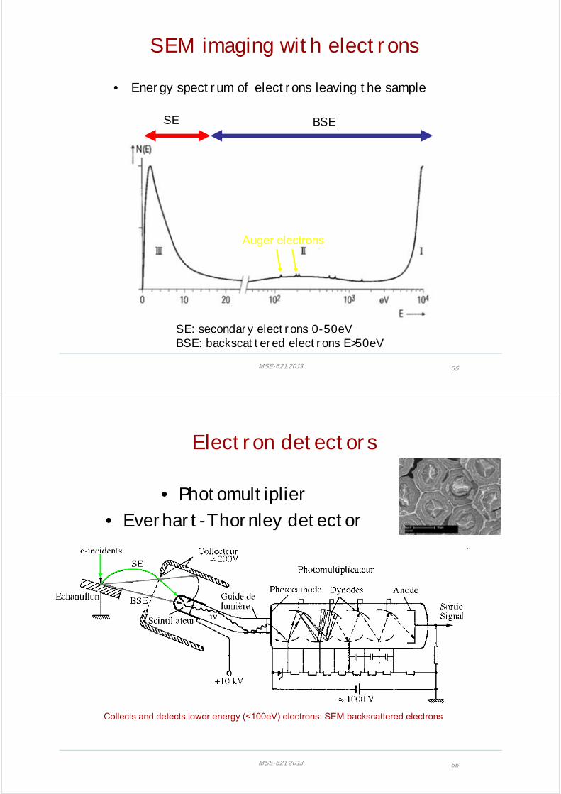
Projector lens system, TEM
mode DIFFRACTION mode IMAGE
• TEM:• Intermediate and
projector lenses– Projection of the
back focal plane to the screen“diffraction”mode
– Projection of the image plane to the screen“image” mode(haute resolution)
MSE-621 2013 45
Projector lens system, TEM
mode DIFFRACTION mode IMAGE
• TEM:• Intermediate and
projector lenses– Projection of the
back focal plane to the screen“diffraction”mode
– Projection of the image plane to the screen“image” mode(haute resolution)
MSE-621 2013 46

Lenses for electrons
• Light: glass lensesdeflection of light throughchanging refraction index
• Charged particlesLorentz Force!Electrostatic lensesMagnetic lenses
• Particularity:Variable focusTunable correctors (astigmatisme)
MSE-621 2013 47
Magnetic lens
• Field with rotational symmetry
• Lorenz Force : F = -e v ^ Be on optical axis: F = 0e not on optical axis : deviatedoptical axis: symmetry axis
• Scherzer 1936:• Magnetic lens with rotational
symmetry:Aberration coefficients:Cs: sphericalCc: chromatical– Always positive !!
4/14/366.0 sres CD
Example: = 0.00197nm, Cs = 1 mmDres = 1.8 10-10 = 1.8ÅResolution limit:
MSE-621 2013 48

Magnetic lens
• Electron optics: no sharp interface at lens « surface »
• No divergent lens !
• Electron beam diverges by itself – Electrostatic repulsion
• “multi-poles” lenses– Correction of aberrations
• “Pole piece”metal cone that confines the magnetic field
• Image rotation !
Pole piece
irone-beam
coil
www.x-raymicroanalysis.com
MSE-621 2013 49
Aberrations:
• Lens aberrations– sperical and chromatical aberrations– Astigmatism– Can be corrected or minimised
• Physical limits– Diffraction effect
Clic
hés:
P.-
A.
Buf
fat
MSE-621 2013 50

chromatical aberration
Focal length varies with energycritical for non-monochromatic beams (advantage for FE guns)
MSE-621 2013 51
Spherical aberration
Focal length depends on the distance from optical axis
Image of the object is dispersed along the optical axis
Circle of least confusion ds = ½ Cs 3
MSE-621 2013 52

Aberrations: astigmatism
Astigmatism: focal length varies in different planes.
MSE-621 2013 53
correctorsAstigmatism:
Light optics: correction with cylindrical lenses
Electron optics:
Correction with quadrupole lenses:2 quadrupole lenses under 45 degree allow to control strenght and direction of correction
Spherical Aberration:
Light optics: correction with combination of convergent and divergent lenses
Electron optics:
Correction with hexapole or quadrupole and octopole lenses
• Cs-corrector
MSE-621 2013 54

Aberrations: diffraction
MSE-621 2013 55
Résolution SEM
• Limite SEM modèrne
MSE-621 2013 56

Resolution: SEM
100
50
10
5
10.5 1 2 5 10 20 30
FE LaB6
W
Tension d'accélération (kV)
Rés
olut
ion
(nm
)
Basse tension/haute résolution: - observation de la surface réelle - échantillons non-métallisés - faible endommagement dû au faisceau
Haute tension/haute résolution: - effets de bord - détails fins non-résolus - fort endommagement dû au faisceau
1985
2000
High voltage, high resolution
Edge effects, fine details not resolved
Beam damage
Low voltage, high resolution
Observation of the real surface
Uncoated samples
Very little beam damage
MSE-621 2013 57
SEM modèrne
• Pour éviter la perte de brillance à basse tension, le canon travaille toujours à tension élevée.
• Pour amener l'énergie des électrons à la valeur souhaitée par l'opérateur, ceux-ci sont ralentis en sortie de colonne (LEO 1500 Gemini)
• La section bleue (beam booster) est au potentiel élevé V0. Noter le changement de polarité entre V0 et VB
MSE-621 2013 58

Resolution of a TEM
• Resolution depends on the aberration of the objetive lens:– Chromatic:
depends on E/E; E @ 300 keV;Cc ~ 1 mm, not critical
– Diffraction: wave lenght = 2 pm @ 300 keV
– Spherical Aberration: limiting !!!
• In 2000: a standard non-corrected TEM 300 keV provides a resolution of ~2Å S
. Pen
nyco
ok e
t al.,
MR
S B
ull.
31, 3
6 (0
6)
MSE-621 2013 59
Electron Microscopy
MSE-621 2013
1. Introduction, types of microscopes, some examples
2. Electron guns, Electron optics3. SEM, interaction volume,
contrasts4. Electron diffraction, X-ray
diffraction5. TEM, contrast, image formation
60

SEM is easy! Just focus and shoot "Photo"!!!
Please comment this picture...
Any idea what itmight be???
MSE-621 2013 61
SEM is easy! Just focus and shoot "Photo"!!!
Does this one sound more obvious?
MSE-621 2013 62

Image formation
MSE-621 2013 63
SEM, signals
X-rayselasticinelastic
Backscattered electrons
e-beam
Secondaryelectrons
photons Auger electrons
IR,UV,vis.
Absorbed current, EBIC
• Secondary electrons(~0-30eV), SE
• Backscattered electrons (~eVo), BSE
• Auger electrons
• Photons: visible, UV, IR,X-rays
• Phonons, Heating
• Absorbtion of incident electrons (EBIC-Current)
MSE-621 2013 64
SEM imaging with electrons
• Energy spectrum of electrons leaving the sample
SE BSE
Auger electrons
SE: secondary electrons 0-50eVBSE: backscattered electrons E>50eV
MSE-621 2013 65
Electron detectors
Collects and detects lower energy (<100eV) electrons: SEM backscattered electrons
• Photomultiplier• Everhart-Thornley detector
MSE-621 2013 66

Electron detectors
• semiconductor
BSE semiconductor detector: a silicon diode with a p-n junction close to its surface collects the BSE (3.8eV/ehole pair)
large collection angleslow (poor at TV frequency)
some diodes are split in 2 or 4 quadrants to bring spatial BSE distribution info
Detects higher energy (>5kV) electrons: SEM backscattered electrons
MSE-621 2013 67
SEM, secondary electrons
• Electrons with low energy (0-50eV) leaving the sample surface
• Intensity depends on inclination of the surface
• topography
MSE-621 2013 68
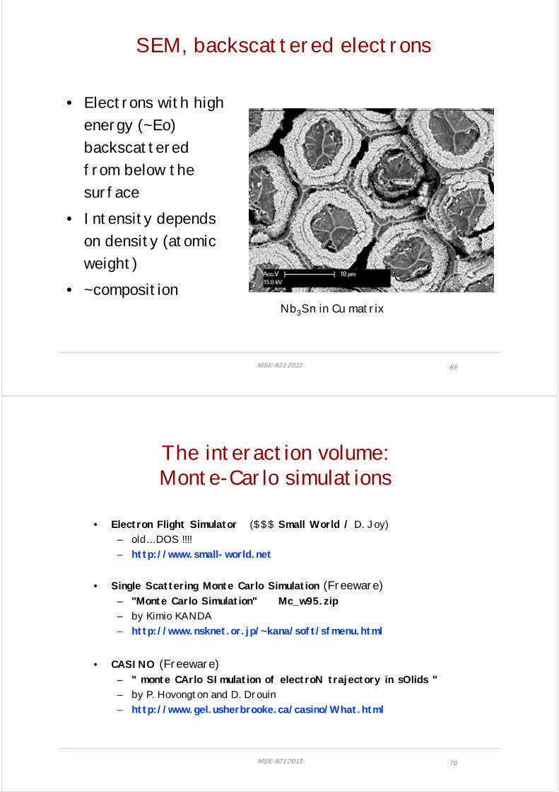
SEM, backscattered electrons
• Electrons with high energy (~Eo) backscattered from below the surface
• Intensity depends on density (atomic weight)
• ~compositionNb3Sn in Cu matrix
MSE-621 2013 69
The interaction volume:Monte-Carlo simulations
• Electron Flight Simulator ($$$ Small World / D. Joy)– old… DOS !!!!– http://www.small-world.net
• Single Scattering Monte Carlo Simulation (Freeware)– "Monte Carlo Simulation" Mc_w95.zip– by Kimio KANDA – http://www.nsknet.or.jp/~kana/soft/sfmenu.html
• CASINO (Freeware)– " monte CArlo SImulation of electroN trajectory in sOlids "– by P. Hovongton and D. Drouin– http://www.gel.usherbrooke.ca/casino/What.html
MSE-621 2013 70

Vacc = 20kV = cte
Depth of electron penetration vs Z and yield of electron backscattering BSE (Monte-Carlo simulation):
Cu 20keV
1
1
C 20keV
1
U 20keV
BSE=6%
BSE=33%
BSE=50%
Penetration and backscatteringvs elements (Z)
MSE-621 2013 71
Z = cteDepth of electron penetration in Cu vs energy E0and yield of electron backscattering BSE (Monte-Carlo simulation):
Cu 20keV
1
Cu 5keV1
Cu 1keV
Cu 1keV
1
BSE=32%
BSE=33%
BSE=35%
MSE-621 2013 72

Vacc = 1kV = cte
Depth of electron penetration vs Z and yield of electron backscattering BSE (Monte-Carlo simulation):
10nm
C 1keV
U 1keV10nm
Cu 1keV
10nm
BSE=14%
BSE=34%
BSE=44%
Penetration and backscattering
MSE-621 2013 73
Vacc = 5kV = cte
Depth of electron penetration vs Z and yield of electron backscattering BSE (Monte-Carlo simulation):
200nm
C 5keV
Cu 5keV
200nm
U 5keV
200nm
BSE=8%
BSE=33%
BSE=47%
Penetration and backscattering
MSE-621 2013 74

SEM: "true" secondary electrons SE1 and "converted BSE" secondaries SE2+SE3
Different types of SE from•SE1: incident probe•SE2: BSE leaving the sample•SE3: BSE hitting the surroundings
The SE signal always contain a high resolution part (SE1 from the probe) and an average (low resolution) part from SE2+SE3!
although this signal is gathered around the probe, its intensity is only attributed to the pixel corresponding to the actual probe position
x0,y0
intensity and delocalisation of SE stemming from the probe at x0,y0 (leadingto the X0,Y0 pixel intensity on the image)
(from L. Reimer, Scanning Electron Microscopy)
MSE-621 2013 75
Relative contribution of SE1 and SE2 (+SE3) vs primary energy
total
total
total
SE1
SE2
The total intensity (green+brown) is attributed to the (x,y) pixel, here at 0 nm on this 1-D model
(adapted from D.C. Joy Hitachi News 16 1989)
MSE-621 2013 76

Yield for SE and BSE emission per incident electron vs atomic number Zsample surface polished (no topography) and perpendicular to the incident beam direction
(intermediate energy E0 15 keV)
SE: low or no chemicalcontrast but for light elementsthe topographical contrast willdominate on rough surfaces
ISE=Ipe· +ISE3
Ipe(pe+pe·sur·)
with the total SE yield, pe the yieldfor SE1 and sur the SE3 yield for materials surrounding the sample (pole-pieces...)
SE1 SE2 SE3
Al Ni
0.11
0.28
(SE1)
BSE: chemical contrast for all the elements (sensitivity Z=0.5)A fast way to phase mapping
IBSE=Ipe· with Ipe the intensity of the primary beam, the BSE yield
MSE-621 2013 77
SE 25 kV BSE
Dust on WC (different Z materialslow Z materialflat material rough material low Z material
thin low Z material
MSE-621 2013 78

MSE-621 2013 79
Relative yield of SE vs angle of incidence on the sample surface
Topographic contrast in SE mode
(0)( ) cos peII I
I0I()
1-10nm
penetration depth ("range") >>SE escape length
(adapted from D.C. Joy Hitachi News 16 1989)
This image cannot currently be displayed.
Autumn 2009 Experimental Methods in Physics Marco CantoniMSE-621 2013 80

Size and edge effects
Do not forget, in SEM:The signal is displayed at the probe position, not at the actual SE production position!!!
intensity profile on image
(adapted from L.Reimer, Scanning Electron Microscopy)
MSE-621 2013 81
(From L. Reimer, Image Formation in Low-Voltage
Scanning Electron Microscopy,
(1993))
MSE-621 2013 82

Tin balls
MSE-621 2013 83
Change in secondary electron contrast withaccelerating voltage
(from L.Reimer, Image formation in the low-voltage SEM)
MSE-621 2013 84

Contraste enhancement at low voltage: less delocalization by SE2. An example: a fracture in Ni-Cr alloy
SE, 5 kV SE, 30 kV
MSE-621 2013 85
SEM low kV imaging
No specimen preparation needed:Low kV imaging of non-conducting, low density samples
FEI MagellanOperator: Ingo GestmannSamples: Marco Cantoni
Al2O3 Nano-crystals
MSE-621 2013 86

SEM low kV imaging
No specimen preparation needed:Low kV imaging of non-conducting, low density samples
FEI MagellanOperator: Ingo GestmannSamples: Marco Cantoni
Al2O3 Nano-crystals
MSE-621 2013 87
SEM low kV imaging
No specimen preparation needed:Low kV imaging of non-conducting, low density samples
FEI MagellanOperator: Ingo GestmannSamples: Marco Cantoni
Carbon nano-tubes(MWCT)
MSE-621 2013 88

SEM low kV imaging
No specimen preparation needed:Low kV imaging of non-conducting samples
Liquid filledorganic membranes
Zeiss Nvision 40Marco Cantoni
MSE-621 2013 89
SEM low kV imaging
No specimen preparation needed:Low kV imaging of non-conducting samples
Liquid filledorganic membranes
Zeiss Nvision 40Marco Cantoni
MSE-621 2013 90

SEM low kV imaging
Purely organic specimen: non-conductive, low density:Metal coating
HeLa Cells, Graham KnottMarco Cantoni, Nvision 40
15nm Ag/Pd coating
3nm Os coating
MSE-621 2013 91
SEM low kV imaging
“Easy” samples:
SC wireNb3Sn in Cu matrix
MSE-621 2013 92

SEM low kV imaging
“classical” conditions: 20kV Everhard-Thornley detector (SE)
Solid state BSEdetector
MSE-621 2013 93
SEM low kV imaging SE and BSE imaging
MSE-621 2013 94

Electron Microscopy
MSE-621 2013
1. Introduction, types of microscopes, some examples
2. Electron guns, Electron optics3. SEM, interaction volume,
contrasts4. Electron diffraction, X-ray
diffraction5. TEM, contrast, image formation
95
Typical TEM
EPFL: Philips CM300
300’000V
MSE-621 2013 96


![HRTEM ontrast nalysis for 6tructure haracterization …...Graphene films were grown on the Ni substrates [4] which were transferred to copper grids for electron microscopy analysis.](https://static.fdocuments.net/doc/165x107/5fd3c7c618ab3b3dc004becb/hrtem-ontrast-nalysis-for-6tructure-haracterization-graphene-films-were-grown.jpg)