Electron Energy-Loss Spectroscopy: A versatile tool for ... · The inelastic scattering of...
29
Electron Energy-Loss Spectroscopy: A versatile tool for the investigations of plasmonic excitations Friedrich Roth, 1,2, * Andreas K¨ onig, 2 J¨ org Fink, 2 Bernd B¨ uchner, 2, 3 and Martin Knupfer 2, † 1 Center for Free-Electron Laser Science / DESY, Notkestraße 85, D-22607 Hamburg, Germany 2 IFW Dresden, P.O. Box 270116, D-01171 Dresden, Germany 3 Institut f¨ ur Festk¨ orperphysik, Technische Universit¨ at Dresden, D-01062 Dresden, Germany (Dated: May 15, 2014) Abstract The inelastic scattering of electrons is one route to study the vibrational and electronic proper- ties of materials. Such experiments, also called electron energy-loss spectroscopy, are particularly useful for the investigation of the collective excitations in metals, the charge carrier plasmons. These plasmons are characterized by a specific dispersion (energy-momentum relationship), which contains information on the sometimes complex nature of the conduction electrons in topical ma- terials. In this review we highlight the improvements of the electron energy-loss spectrometer in the last years, summarize current possibilities with this technique, and give examples where the investigation of the plasmon dispersion allows insight into the interplay of the conduction electrons with other degrees of freedom. * [email protected] † [email protected] 1 arXiv:1405.3369v1 [cond-mat.mtrl-sci] 14 May 2014
Transcript of Electron Energy-Loss Spectroscopy: A versatile tool for ... · The inelastic scattering of...

Electron Energy-Loss Spectroscopy: A versatile tool for the
investigations of plasmonic excitations
Friedrich Roth,1, 2, ∗ Andreas Konig,2 Jorg Fink,2 Bernd Buchner,2, 3 and Martin Knupfer2, †
1Center for Free-Electron Laser Science / DESY,
Notkestraße 85, D-22607 Hamburg, Germany
2IFW Dresden, P.O. Box 270116, D-01171 Dresden, Germany
3Institut fur Festkorperphysik, Technische Universitat Dresden, D-01062 Dresden, Germany
(Dated: May 15, 2014)
Abstract
The inelastic scattering of electrons is one route to study the vibrational and electronic proper-
ties of materials. Such experiments, also called electron energy-loss spectroscopy, are particularly
useful for the investigation of the collective excitations in metals, the charge carrier plasmons.
These plasmons are characterized by a specific dispersion (energy-momentum relationship), which
contains information on the sometimes complex nature of the conduction electrons in topical ma-
terials. In this review we highlight the improvements of the electron energy-loss spectrometer in
the last years, summarize current possibilities with this technique, and give examples where the
investigation of the plasmon dispersion allows insight into the interplay of the conduction electrons
with other degrees of freedom.
∗ [email protected]† [email protected]
1
arX
iv:1
405.
3369
v1 [
cond
-mat
.mtr
l-sc
i] 1
4 M
ay 2
014
CONTENTS
I. Introduction 2
II. Instrumentation 4
A. Working Principle 4
B. Scattering Theory - The EELS Cross Section 6
C. Experimental Details 10
1. The Spectrometer 10
2. Sample Preparation 13
III. Selected Results: The investigation of plasmons in topical materials 15
A. Peculiar plasmon dispersion in potassium intercalated picene 16
B. Negative plasmon dispersion in the charge density wave compound 2H-TaSe2 18
C. Unusual plasmon behavior in the spin-ladder cuprate CaxSr14−xCu24O41 20
IV. Summary 24
V. Acknowledgments 25
References 25
I. INTRODUCTION
The exploration of the electronic properties of topical materials represents a major task
in condensed matter physics and beyond. Various experimental and theoretical approaches
have been developed and steadily improved throughout the last decades. Concerning the
experimental techniques, inelastic scattering of particles has become one important branch
in order to analyze the electronic excitation spectrum of materials. They often offer the
beauty to independently select the scattering angle, and in this way to allow momentum
dependent studies of the particular electronic excitation. Inelastic scattering experiments of
electron systems require that the probe particles interact with the electrons of the materials
under investigation. Therefore two, actually complementary inelastic methods are applied,
in particular in condensed matter physics, which are inelastic electron scattering, also called
2

electron energy-loss spectroscopy (EELS) [1–3], and inelastic light scattering, termed with
various acronyms in dependence of the light energy used (Raman scattering, x-ray Raman
scattering, inelastic x-ray scattering (IXS)) [4–6].
In this article we describe some recent application of EELS in transmission for the in-
vestigation of the collective density excitation of electron gases, the plasmons. In general,
EELS is known for many years and has been applied to study the excitations of core elec-
tron, valence electrons and vibrations/phonons. This is closely related to the equipment and
spectrometers used.
The application of EELS in transmission electron microscopes (TEM) represents one
important branch [7–10]. It has been proven to be very useful to detect the chemical and
structural composition of the material under scrutiny in combination with a very high lateral
resolution. Thereby, core level excitations are predominantly used. Also, using energy filters
in combination with microscopy can enhance particular contrasts in the TEM images. The
resolution capability of the EELS option in microscopes has been improved during the last
years, and also valence band excitation come into the focus of researchers. We note however,
that in most cases EELS studies in transmission electron microscopes are not carried out as
a function of momentum.
High resolution electron energy-loss spectroscopy (HREELS) carried out in a reflection
geometry represents another branch of EELS [11–13]. In this case, the electrons are backscat-
tered from a sample surface where they undergo the inelastic scattering process. The primary
electron energies used in HREELS are quite low, often in the range of 10 eV or lower. Low
energies are chosen to achieve very high energy resolution down to or even less than 1 meV,
which renders it possible to study electronic excitations in detail as well as surface vibra-
tions. One of the most important application of HREELS is the investigation of adsorbates
on crystal surfaces with many interesting aspects ranging from fundamental surface science
to application related questions in ,e. g., catalysis. Applying HREELS it should always be
kept in mind that one is dealing with a very surface sensitive technique, the scattered elec-
trons do hardly penetrate the material. As a consequence, the excitations studied are surface
excitations only, and these can be very different from their bulk counterparts in particular
for electronic excitations.
In this contribution, we report on studies using a dedicated spectrometer for EELS in
transmission with state-of-the-art resolution parameters and with the option to vary the
3

sample temperature in a rather wide range. In order to elucidate the current status we sum-
marize recent investigations of the behavior of charge carrier plasmons in topical materials,
and we discuss the physical insight that is provided by such investigations. The excitation of
plasmons, the longitudinal collective excitations of the charge carriers in metals is a specialty
of EELS (or IXS) [1, 2, 4, 14], as it cannot be achieved by light absorption techniques. EELS
however is not restricted to the investigation of plasmons, also other excitations such as ex-
citons or inter-band transition can provide valuable information, in particular when probed
as a function of momentum transfer [15–26]. In addition, we note that the momentum de-
pendence of electronic excitations can be governed by crystal local field effects, a topic that
is also studied using EELS in transmission and as a function of momentum transfer [27–29].
II. INSTRUMENTATION
A. Working Principle
E0,k0
Incoming ElectronSample
Θ
k0
E1,k1
Scattered Electron
q⊥
q‖
q
γ
FIG. 1. The basic scheme for an EELS experiment in transmission. The electrons with an energy
E0 and an incoming momentum k0 are focused on the thin sample and scattered under an angle
θ. During the scattering event both a momentum transfer q and an energy transfer ω can occur in
the sample. It is possible to perform elastic scattering (Bragg scattering) too by setting the energy
loss to zero.
The basic scattering geometry of an electron scattering experiment in transmission is
4

shown in Fig. 1. A beam of rather fast electrons, specified by a momentum hk0, is focused
on a thin (≈ 100 nm) film of the material under investigation. While passing through this
sample a fraction of the beam electrons is inelastically scattered by an angle θ away from
the initial direction. This leads to a momentum- (hq) and energy-transfer (hω) given by
hq = hk0 − hk1 (1)
and
hω = E0 − E1 =h2(k2
0 − k21)
2m(2)
and will as a consequence leave the sample in an excited state, which is characterized by the
energy and momentum it acquired from the electrons of the primary beam.
According to Fig. 1 the momentum transfer q can be decomposed into components parallel
and perpendicular to the incoming momentum k0
q2 = q2‖ + q2⊥. (3)
It is important to realize that the primary energy of the electrons is rather high (the spec-
trometer described in this contribution works with E0 = 172 keV). This leads to a large
value of k0 ∼ 230 A−1. Comparing this to a typical extension of a Brillouin zone inside a
solid, which is of the order 1 A−1, one arrives at small scattering angles θ and therefore
q⊥ = k1 sin θ ∼= k1θ ∼= k0θ. (4)
Furthermore, the cosine theorem yields (cf. Fig. 1)
k21 = k20 + q2 − 2k0q cos γ ∼= k20 − 2k0q cos γ. (5)
Therefore q‖ is related to the energy-loss by
hω ∼=h2(k20 − k21)
2m∼=hk0m· q cos γ =
hk0m· q‖. (6)
5

For a typical energy loss around hω ∼ 10 eV and at experimentally used scattering angles
of θ ∼ 0.25, we obtain the important result
q‖q⊥
=mω
hk20θ∼ 10−3 (7)
and so the momentum transfer can be regarded as lying completely within the plane which is
perpendicular to the incoming electron beam. To obtain information beyond this particular
plane one has to rotate the sample with respect to the beam or one has to select other polar
directions of k1. Another very important conclusion is that q ∼ q⊥ remains valid over a large
energy range (up to 100 eV). This fact is essential for a correct evaluation of the dispersion
measurements as well as the Kramers-Kronig analysis.
In addition to the possibility of inelastic scattering processes with non-zero energy-loss
it is also possible to perform elastic scattering (Bragg scattering) by setting the energy-
loss to zero. This allows the analysis of the crystal structure and is an important tool for
investigations of single-crystals where the electronic properties may depend on the direction
in the reciprocal lattice.
B. Scattering Theory - The EELS Cross Section
The essential quantity which is actually measured in the EELS experiment is the doubly
differentiated cross section
d2σ
dΩdω,
which gives the probability of detecting an electron in a scattering angle element dΩ having
lost an energy dω compared to its initial energy E0. Quantum mechanically, the scattering
process can be described by a transition from an initial state |n0, k0〉 (incident electron plus
electrons in the solid in the ground state) to a final state |n1, k1〉 (outgoing electron plus
excited electrons in the solid). The interaction of the scattered electrons with the charges
in the sample is driven by the Coulomb potential which (in momentum space) is given by
Hint =e2
q2.
6

Due to their high kinetic energy, the incident electrons are distinguishable from electrons in
the solid and only weak interactions of the electrons with the sample have to be considered.
Then the differential cross-section can be written in the Born approximation [30, 31]
d2σ
dΩdω=∑n0,n1
|〈n1, k1|Hint|n0, k0〉|2 δ(En0 + E0 − En1 − E1) (8)
with the initial (final) states of the incoming (outgoing) electrons and the corresponding
states for the sample |nl〉. The initial and final states can be written as simple products
which leads to a new equation for the differential cross-section
d2σ
dΩdω=
(dσ
dΩ
)Ruth
· S(q, ω), (9)
where
(dσ
dΩ
)Ruth
=4
a20q4
is the elastic Rutherford cross-section with a0 being the Bohr radius. The dynamic structure
factor S(q, ω) is defined by
S(q, ω) =1
N
∑n0,n1
pn0
∣∣∣∣∣〈n1|∑j
eiqrj |n0〉
∣∣∣∣∣2
δ(En0 − En1 + ω). (10)
The factor 1/N has been included because the cross-section is defined per electron. This
close relationship between the dynamic structure factor and the density-density correlation
function was first derived by Van Hove [30].
With the help of the Kubo formalism of linear-response theory [32, 33] and the fluctuation-
dissipation theorem [34, 35] one may establish a relation between the dynamic structure
factor S(q, ω) and the dielectric function ε(q, ω). This is an example of a very general
principle in statistical physics, namely the fluctuation-dissipation theorem which always
connects some sort of correlation function (the density-density correlation in this case) with
a response function (ε(q, ω))
7
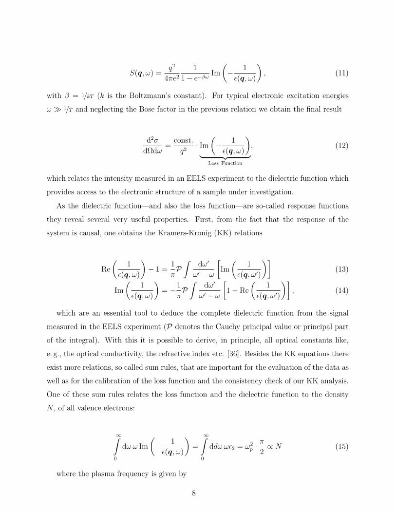
S(q, ω) =q2
4πe21
1− e−βωIm
(− 1
ε(q, ω)
), (11)
with β = 1/kT (k is the Boltzmann’s constant). For typical electronic excitation energies
ω 1/T and neglecting the Bose factor in the previous relation we obtain the final result
d2σ
dΩdω=
const.
q2· Im
(− 1
ε(q, ω)
)︸ ︷︷ ︸
Loss Function
, (12)
which relates the intensity measured in an EELS experiment to the dielectric function which
provides access to the electronic structure of a sample under investigation.
As the dielectric function—and also the loss function—are so-called response functions
they reveal several very useful properties. First, from the fact that the response of the
system is causal, one obtains the Kramers-Kronig (KK) relations
Re
(1
ε(q, ω)
)− 1 =
1
πP∫
dω′
ω′ − ω
[Im
(1
ε(q, ω′)
)](13)
Im
(1
ε(q, ω)
)= − 1
πP∫
dω′
ω′ − ω
[1− Re
(1
ε(q, ω′)
)], (14)
which are an essential tool to deduce the complete dielectric function from the signal
measured in the EELS experiment (P denotes the Cauchy principal value or principal part
of the integral). With this it is possible to derive, in principle, all optical constants like,
e. g., the optical conductivity, the refractive index etc. [36]. Besides the KK equations there
exist more relations, so called sum rules, that are important for the evaluation of the data as
well as for the calibration of the loss function and the consistency check of our KK analysis.
One of these sum rules relates the loss function and the dielectric function to the density
N , of all valence electrons:
∞∫0
dω ω Im
(− 1
ε(q, ω)
)=
∞∫0
ddω ωε2 = ω2p ·π
2∝ N (15)
where the plasma frequency is given by
8

ωp =
√4πNe2
me
. (16)
Thus, the strengths of possible transitions are not independent from each other but are
balanced in a way that enhancing the weight in a particular energy range of the spectrum
by, e. g., the appearance of a phase transition will reduce the intensity in another energy
window to keep the above given integral at a constant value. In practice, calculations as
well as experiments are of course always restricted to a finite energy window and one may
evaluate partial sum-rules according to
ω1∫ω0
dωω Im
(− 1
ε(q, ω)
)= ω2
p ·π
2(Neff/N),
that provide access to an effective number of charge carriers Neff contributing to a particular
type of excitation within a given energy range.
Finally, for metallic systems a further sum rule can be employed [31], which may allow
an additional check of the data analysis:
∞∫0
dωIm(− 1ε(q,ω)
)ω
=π
2. (17)
Moreover, measurements of the resistivity represent another way to observe how several
degrees of freedom influence the conduction electrons. Interestingly, there exist a simple re-
lation between the resistivity (reciprocal value of the (DC)-conductivity σ) and the plasmon
properties:
σ = ω2p · ε0 · τ, (18)
where ε0 is the background dielectric constant and τ displays the scattering rate (corre-
lated with the width of the plasmon) [37].
9
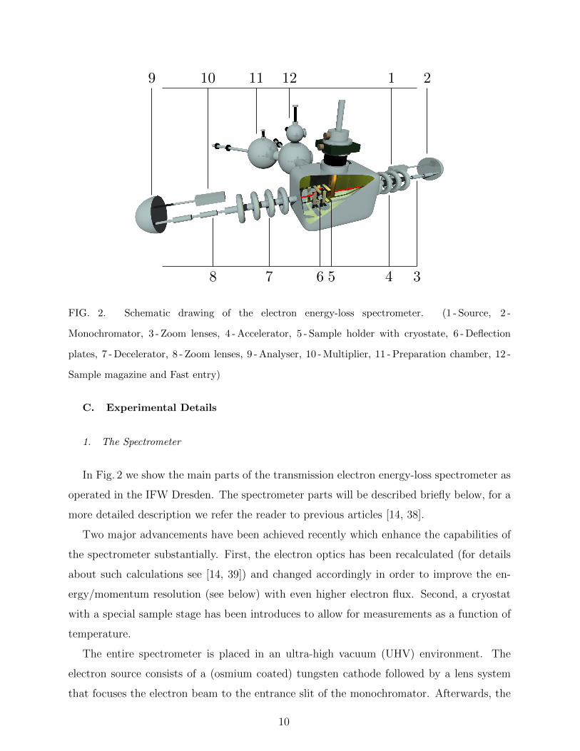
1 29 10 11 12
345678
FIG. 2. Schematic drawing of the electron energy-loss spectrometer. (1 - Source, 2 -
Monochromator, 3 - Zoom lenses, 4 - Accelerator, 5 - Sample holder with cryostate, 6 - Deflection
plates, 7 - Decelerator, 8 - Zoom lenses, 9 - Analyser, 10 - Multiplier, 11 - Preparation chamber, 12 -
Sample magazine and Fast entry)
C. Experimental Details
1. The Spectrometer
In Fig. 2 we show the main parts of the transmission electron energy-loss spectrometer as
operated in the IFW Dresden. The spectrometer parts will be described briefly below, for a
more detailed description we refer the reader to previous articles [14, 38].
Two major advancements have been achieved recently which enhance the capabilities of
the spectrometer substantially. First, the electron optics has been recalculated (for details
about such calculations see [14, 39]) and changed accordingly in order to improve the en-
ergy/momentum resolution (see below) with even higher electron flux. Second, a cryostat
with a special sample stage has been introduces to allow for measurements as a function of
temperature.
The entire spectrometer is placed in an ultra-high vacuum (UHV) environment. The
electron source consists of a (osmium coated) tungsten cathode followed by a lens system
that focuses the electron beam to the entrance slit of the monochromator. Afterwards, the
10
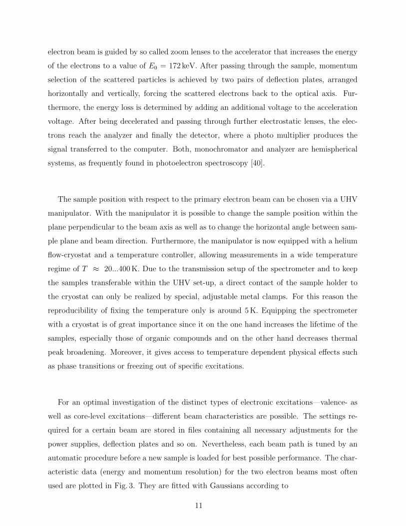
electron beam is guided by so called zoom lenses to the accelerator that increases the energy
of the electrons to a value of E0 = 172 keV. After passing through the sample, momentum
selection of the scattered particles is achieved by two pairs of deflection plates, arranged
horizontally and vertically, forcing the scattered electrons back to the optical axis. Fur-
thermore, the energy loss is determined by adding an additional voltage to the acceleration
voltage. After being decelerated and passing through further electrostatic lenses, the elec-
trons reach the analyzer and finally the detector, where a photo multiplier produces the
signal transferred to the computer. Both, monochromator and analyzer are hemispherical
systems, as frequently found in photoelectron spectroscopy [40].
The sample position with respect to the primary electron beam can be chosen via a UHV
manipulator. With the manipulator it is possible to change the sample position within the
plane perpendicular to the beam axis as well as to change the horizontal angle between sam-
ple plane and beam direction. Furthermore, the manipulator is now equipped with a helium
flow-cryostat and a temperature controller, allowing measurements in a wide temperature
regime of T ≈ 20...400 K. Due to the transmission setup of the spectrometer and to keep
the samples transferable within the UHV set-up, a direct contact of the sample holder to
the cryostat can only be realized by special, adjustable metal clamps. For this reason the
reproducibility of fixing the temperature only is around 5 K. Equipping the spectrometer
with a cryostat is of great importance since it on the one hand increases the lifetime of the
samples, especially those of organic compounds and on the other hand decreases thermal
peak broadening. Moreover, it gives access to temperature dependent physical effects such
as phase transitions or freezing out of specific excitations.
For an optimal investigation of the distinct types of electronic excitations—valence- as
well as core-level excitations—different beam characteristics are possible. The settings re-
quired for a certain beam are stored in files containing all necessary adjustments for the
power supplies, deflection plates and so on. Nevertheless, each beam path is tuned by an
automatic procedure before a new sample is loaded for best possible performance. The char-
acteristic data (energy and momentum resolution) for the two electron beams most often
used are plotted in Fig. 3. They are fitted with Gaussians according to
11
Inte
nsi
ty (
arb
. un
its)
-0.3 -0.2 -0.1 0.0 0.1 0.2 0.3
Energy (eV)
beam A
beam B
Inte
nsity
(ar
b.un
its)
-0.10 0.00 0.10
Momentum Transfer (1/Å)
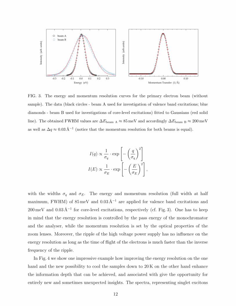
FIG. 3. The energy and momentum resolution curves for the primary electron beam (without
sample). The data (black circles - beam A used for investigation of valence band excitations; blue
diamonds - beam B used for investigations of core-level excitations) fitted to Gaussians (red solid
line). The obtained FWHM values are ∆Ebeam A ≈ 85 meV and accordingly ∆Ebeam B ≈ 200 meV
as well as ∆q ≈ 0.03 A−1 (notice that the momentum resolution for both beams is equal).
I(q) ∝ 1
σq· exp
[−(q
σq
)2]
I(E) ∝ 1
σE· exp
[−(E
σE
)2],
with the widths σq and σE. The energy and momentum resolution (full width at half
maximum, FWHM) of 85 meV and 0.03 A−1 are applied for valence band excitations and
200 meV and 0.03 A−1 for core-level excitations, respectively (cf. Fig. 3). One has to keep
in mind that the energy resolution is controlled by the pass energy of the monochromator
and the analyser, while the momentum resolution is set by the optical properties of the
zoom lenses. Moreover, the ripple of the high voltage power supply has no influence on the
energy resolution as long as the time of flight of the electrons is much faster than the inverse
frequency of the ripple.
In Fig. 4 we show one impressive example how improving the energy resolution on the one
hand and the new possibility to cool the samples down to 20 K on the other hand enhance
the information depth that can be achieved, and associated with give the opportunity for
entirely new and sometimes unexpected insights. The spectra, representing singlet excitons
12

Los
s fu
ncti
on (
arb.
uni
ts)
3.02.82.62.42.22.01.81.61.41.21.0
Energy (eV)
DE = 185 meV, 300 K DE = 80 meV, 300 K DE = 80 meV, 20 K
pentacene
q = 0.1 Å-1
q || a*
Los
s fu
ncti
on (
arb.
uni
ts)
3.02.82.62.42.22.01.81.61.41.21.0
Energy (eV)
DE = 185 meV, 300 K DE = 80 meV, 300 K DE = 80 meV, 20 K
pentacene
q = 0.1 Å-1
q || b*
FIG. 4. Comparison of the loss function of pentacene single crystals for q ‖ a∗ (left panel) and
q ‖ b∗ (right panel) as a function of the energy resolution of the used electron beam (red circles)
as well as the temperature (black squares - room temperature, blue diamonds - 20 K).
in pentacene for small momentum transfer along the fundamental reciprocal lattice vectors,
which were measured some years ago with an energy resolution of about 185 meV at 300 K
show now visible structure and are represented by a broad asymmetric feature [20]. The
situation changes significantly by measuring the equivalent spectra with a better energy
resolution of 80 meV and further by cooling the samples down to 20 K. As shown in Fig. 4 one
now can identify a fine structure in the energy range of the former broad excitation feature
(for further reading see Ref. [41]). Thus, the much higher resolution allows the identification
of several excitonic/ vibronic features, the exact nature of which is not completely understood
yet.
2. Sample Preparation
One of the major challenges in the application of EELS in transmission in solid-state
physics and material science is the preparation of the samples. The mean free path of elec-
trons in solids is limited due to a number of interactions, predominantly plasmon excitations
[7, 42–45].
Therefore samples with a thickness of only about 100 nm are required and form the main
criterion whether or not a system can be investigated by EELS. Furthermore, the electron
beam in the spectrometer described here has a focal size of the order of 0.5 mm2, i. e. the
samples also must have a similar lateral extension. There exist several possibilities to obtain
13
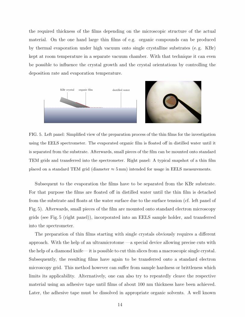
the required thickness of the films depending on the microscopic structure of the actual
material. On the one hand large thin films of e.g. organic compounds can be produced
by thermal evaporation under high vacuum onto single crystalline substrates (e. g. KBr)
kept at room temperature in a separate vacuum chamber. With that technique it can even
be possible to influence the crystal growth and the crystal orientations by controlling the
deposition rate and evaporation temperature.
KBr crystal organic film destilled water
FIG. 5. Left panel: Simplified view of the preparation process of the thin films for the investigation
using the EELS spectrometer. The evaporated organic film is floated off in distilled water until it
is separated from the substrate. Afterwards, small pieces of the film can be mounted onto standard
TEM grids and transferred into the spectrometer. Right panel: A typical snapshot of a thin film
placed on a standard TEM grid (diameter ≈ 5 mm) intended for usage in EELS measurements.
Subsequent to the evaporation the films have to be separated from the KBr substrate.
For that purpose the films are floated off in distilled water until the thin film is detached
from the substrate and floats at the water surface due to the surface tension (cf. left panel of
Fig. 5). Afterwards, small pieces of the film are mounted onto standard electron microscopy
grids (see Fig. 5 (right panel)), incorporated into an EELS sample holder, and transferred
into the spectrometer.
The preparation of thin films starting with single crystals obviously requires a different
approach. With the help of an ultramicrotome —a special device allowing precise cuts with
the help of a diamond knife— it is possible to cut thin slices from a macroscopic single crystal.
Subsequently, the resulting films have again to be transferred onto a standard electron
microscopy grid. This method however can suffer from sample hardness or brittleness which
limits its applicability. Alternatively, one can also try to repeatedly cleave the respective
material using an adhesive tape until films of about 100 nm thickness have been achieved.
Later, the adhesive tape must be dissolved in appropriate organic solvents. A well known
14

example would be the preparation of thin graphite samples [46], where it is even possible to
thin the crystal down to a monolayer of graphene (also called exfoliation of graphene [47]).
I
FIG. 6. Left panel: Schematic drawing of a sample holder and the in situ doping with alkali
metals evaporated from commercial getter sources. Right panel: Snapshot of the construction in
the vacuum chamber. At the bottom of the picture one can see the holder for the getter sources
(notice that the fifth getter is in an operating state). Furthermore, one can identify the transfer
rod with a sample holder on top as well as the oven in the upper part of the picture.
In addition, the UHV set-up of our EELS spectrometer including a preparation chamber
also enables to further modify the samples by for instance heating to temperatures up to
about 800 K in a dedicated sample furnace and under inert conditions. Another option
is the evaporation of further materials onto the samples, e. g., it is possible to intercalate
the particular samples with alkali metals in the preparation chamber. For this, the sample
is exposed to an alkali metal atmosphere from commercially available alkali metal getter
sources (distance between getter source and sample is about 30 mm)(cf. Fig. 6).
III. SELECTED RESULTS: THE INVESTIGATION OF PLASMONS IN TOPI-
CAL MATERIALS
The most prominent excitations of the electron gas for small momentum transfers are
collective oscillations. Quantum-mechanically these excitations are described as quasi par-
ticles and are called plasmons. In consideration of the conduction electrons as a quasi-free
15
electron gas, the density of this electron gas is unstable towards an external electrostatic
perturbation at a characteristic frequency, i. e., it will oscillate at this characteristic fre-
quency ωp (see Eq. 16) like a harmonic oscillator provided that its wavelength is longer than
a characteristic cutoff 1/qc, which is determined by the decay of the density oscillations into
intra-band excitations (n is the density of the electron gas, e denotes the elementary charge,
ε∞ the background dielectric screening due to interband excitations, and m∗ the (optical)
effective mass of the charge carriers). The quanta of these collective density fluctuations
were first coined plasmons by David Pines in Ref. [48].
A feature of special importance related to plasmons is the momentum dependence of the
plasma frequency, i. e., the plasmon dispersion which can be derived from the Lindhard func-
tion under some assumptions [49–51]. As a result, the plasmon dispersion can be expanded
into a Taylor series at q = 0 given by
ω(qqq) = ωp + αqqq2 +O(qqq4); α ∝ v2F , (19)
where vF is the mean Fermi velocity. This is the generic behavior of the collective plasmon
modes in the random phase approximation (RPA) and there are numerous examples in the
literature, that this shape of plasmon dispersion is realized for different simple metals, such
as Li and Na [52] as well as for more complex structures, such as the planar cuprates, e. g.,
Bi2Sr2CaCu2O8 [53]. However, there are also examples for anomalous dispersions, varying
from linear to even negative slope. They contain important physical information on the
modification of the electron gas by other degrees of freedom in the material. This will be
further emphasized in the following sections, which demonstrate that EELS is a versatile
spectroscopic method for the study of condensed matter and has become a standard method
for investigating the collective excitations of electrons.
A. Peculiar plasmon dispersion in potassium intercalated picene
In the next section we present measurements on a recently reported organic supercon-
ductor, potassium doped picene [54]. Picene (C22H14) is a molecule that consists of five
benzene rings arranged in a zigzag like manner and forms a herringbone, monoclinic crystal
structure, similar to other aromatic molecules [55].
16
The addition of potassium results in a charge transfer of the outer s electrons to the
picene molecules, i. e., a doping of the molecular crystal. For such crystals superconductiv-
ity has been reported with a transition temperature up to 18 K [54], which is rather high
as compared to many other doped molecular crystals or charge transfer salts. The only
molecular materials that shows superconductivity at higher temperatures are the fullerides,
the discovery of which represented a breakthrough in the field of superconductivity [56, 57].
norm
. Int
ensi
ty (
arb.
uni
ts)
10987654321Energy (eV)
undoped picene potassium doped picene
norm
. Int
ensi
ty (
arb.
uni
ts)
4.03.53.02.52.01.51.00.5
Energy (eV)
q (1/Å)
0.1
0.2
0.3
0.4
0.5
0.6
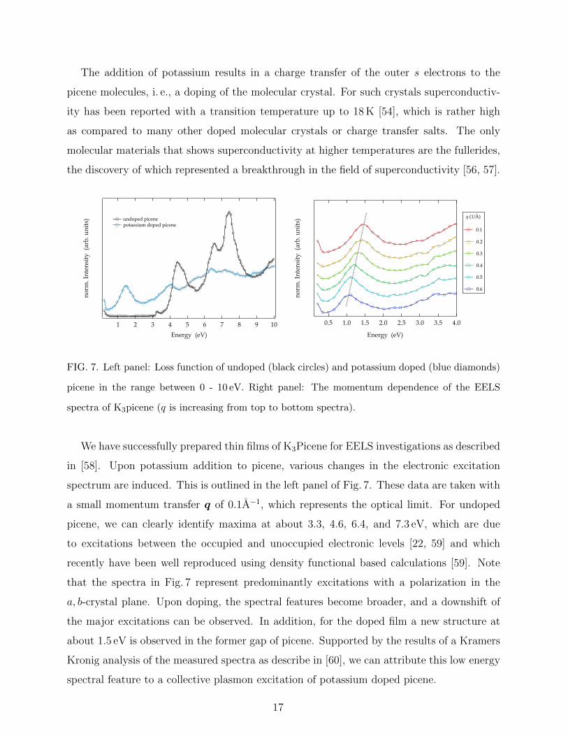
FIG. 7. Left panel: Loss function of undoped (black circles) and potassium doped (blue diamonds)
picene in the range between 0 - 10 eV. Right panel: The momentum dependence of the EELS
spectra of K3picene (q is increasing from top to bottom spectra).
We have successfully prepared thin films of K3Picene for EELS investigations as described
in [58]. Upon potassium addition to picene, various changes in the electronic excitation
spectrum are induced. This is outlined in the left panel of Fig. 7. These data are taken with
a small momentum transfer q of 0.1A−1, which represents the optical limit. For undoped
picene, we can clearly identify maxima at about 3.3, 4.6, 6.4, and 7.3 eV, which are due
to excitations between the occupied and unoccupied electronic levels [22, 59] and which
recently have been well reproduced using density functional based calculations [59]. Note
that the spectra in Fig. 7 represent predominantly excitations with a polarization in the
a, b-crystal plane. Upon doping, the spectral features become broader, and a downshift of
the major excitations can be observed. In addition, for the doped film a new structure at
about 1.5 eV is observed in the former gap of picene. Supported by the results of a Kramers
Kronig analysis of the measured spectra as describe in [60], we can attribute this low energy
spectral feature to a collective plasmon excitation of potassium doped picene.
17
The dispersion of the charge carrier plasmon in K3Picene is presented in the right panel
of Fig. 7. It can be seen that the plasmon dispersion is clearly negative, which deviates
from the traditional picture of metals based on the homogeneous electron gas, where the
plasmon dispersion should be quadratic and positive (see discussion above). Interestingly,
previous investigations of the plasmon dispersion in another doped molecular crystal, K3C60,
have also revealed an unusual behavior of the plasmon as it is characterized by a vanishing
momentum dependence [61, 62].
For molecular solids there exists an important difference to free electron gas metals,
which is the strong localization of the conduction electron wave functions to the molecules
with little resemblance to a homogeneous distribution. As a consequence, the momentum
dependence of the dielectric function and thus the loss function too is different for molecular
crystals and those with homogeneous electron gases. In other words, in molecular solids
there is strong competition between charge localization and metallicity. This can cause the
bare plasmon dispersion for doped molecular solids to be negative [63]. However, there
is even more to be considered for molecular solids. Energetically higher lying inter-band
transitions show a quite substantial momentum dependence in their spectral weight, which
again is a consequence of the localized wave functions in these materials. As these inter-band
transitions represent the dielectric background (screening) of the charge carrier plasmon,
they can counteract and even cancel the negative plasmon dispersion [62, 63]. Finally, since
molecular solids have quite inhomogeneous electron systems, also crystal local-field effects
have to be considered, which are related to the fact that the polarization due to an external
perturbation fluctuates on the atomic scale and the spatial average of the perturbing field is
not the same [62–64]. In dependence of the exact crystal packing and molecular structure,
in some cases they can even support a negative plasmon dispersion [62–64].
B. Negative plasmon dispersion in the charge density wave compound 2H-TaSe2
2H-TaSe2 is a member of the large family of transition metal dichalcogenides, in which
many and very interesting physical phenomena occur and can be studied [65–67]. The
general stoichiometry is TX2 with a transition metal T=Ti, Nb, Ta, etc. bound to two
chalcogenides X=S, Se, Te. All members show layered structures with only weak van der
Waals interlayer interactions and a stacking X-T-X. In addition, the layering allows several
18

geometrical arrangements leading to numerous polymorphs. Depending on the exact com-
position of the material, various ground states such as semiconductors (e. g. MoS2 or WS2),
metals (TaSe2, NbSe2), superconductors (e. g. NbS2) or charge density waves (e. g. TaSe2
or NbSe2) are realized [65, 66].
The compound discussed in the following, 2H-TaSe2, shows a charge density wave (CDW)
phase transition by cooling down below 120 K [66, 68]. The electronic excitations, in par-
ticular the behavior of the charge carrier plasmon in 2H-TaSe2 have been studied recently
using EELS as a function of momentum and temperature. Its energy-loss spectrum in the
low energy range is governed by a collective charge carrier plasmon excitation at around 1 eV
(cf. Fig. 8 left panel). The dominant feature at 21 eV can be associated to the volume plas-
mon, while the excitations at even higher energies (around 40 eV) arise from Ta core-level
excitations as well as from multiple scattering of the lower lying excitations.
Inte
nsity
(ar
b. u
nits
)
1009080706050403020100
Energy (eV)
Inte
nsity
(arb
. uni
ts)
43210Energy (eV)
T = 300 K
q = 0.1 -1
Inte
nsity
(ar
b. u
nits
)
3.53.02.52.01.51.00.50.0
Energy (eV)
1.0
0.9
0.8Ener
gy /
wP
1.51.00.5Mom. Transfer / Q
q (1/)
0.1 0.125 0.15 0.175 0.2 0.225 0.25 0.275 0.3 0.4 0.5
2H-TaSe2
FIG. 8. Left panel: Energy-loss spectrum of 2H-TaSe2 over a broad energy range, corrected for the
elastic line contribution. The inset shows a detailed view of the low energy regime with the 1 eV
charge-carrier plasmon. Right panel: Loss spectra for 2H-TaSe2 at different momentum transfers
in the regime of 0.1 to 0.5A−1. The inset shows the peak position normalised to ωp in energy as
well as to the CDW ordering vector’s absolute value Q in momentum transfer.
The behavior of the plasmon as a function of momentum in 2H-TaSe2 is very surprising.
As can be seen in Fig. 8 (right panel) the plasmon dispersion is negative up to a momentum
value of about 0.7 A−1 where it starts to level off or to increase slightly [69]. In general,
negative plasmon dispersions have been demonstrated in several other materials, among
them molecular crystals (see discussion above) but also the heavier alkali metals [70, 71].
19

The presence of a negative plasmon dispersion in 2H-TaSe2 with a CDW ground state,
and the contrary observation for 2H-NbS2 [72], which does not show a phase transition
into a low temperature CDW phase, might indicate the importance of charge density wave
fluctuations for the momentum dependent behavior of the plasmon. Since the plasmon mode
involves a redistribution of electronic charge, it can be strongly coupled to the fluctuations
of the charge ordered state, in other words the two density “waves” compete for the same
electrons. In an empirical model put forward recently, the energy required for the excitation
of a particular plasmon mode decreases as its wave vector more closely coincides with the
preferred wave vector of the charge ordered state and its fluctuations [69]. The plasmon
dispersion is affected whenever the tendency towards electronic order defines a preferred
wave vector for the charge density fluctuations. This may thus represent a novel signature
of electronic order. It may therefore be expected that the plasmons in a large class of charge
ordered materials will develop a signature of the electronic order in their dispersions, in close
analogy to that observed in the studied group of transition-metal dichalcogenides.
In contrast, recent calculations of the plasmon dispersion in 2H-TaSe2 and related ma-
terials based on density functional theory argue in a different direction [73]. There, the
negative plasmon dispersion as observed for 2H-TaSe2 is a consequence of the band struc-
ture in these compounds, where the conduction electrons occupy bands derived from d-levels.
It has been concluded that the negative plasmon dispersion results from a peculiar behavior
of the intraband transitions within the d-derived conduction bands, that give rise to the
plasmon, which are very different from those of a homogeneous electron gas. Since the band
structure of many 2H polymorphs of the transition metal dichalcogenides is very similar,
a negative plasmon dispersion should be a common behavior of these compounds. This
conclusion however contradicts the reported positive plasmon dispersion in 2H-NbS2 [72],
but it has been argued that this could be due to a non-stoichiometric sample in this case.
Therefore, the microscopic origin of the negative plasmon dispersion in 2H-TaSe2 still is not
understood, and the subject asks for further investigations in order to solve this issue.
C. Unusual plasmon behavior in the spin-ladder cuprate CaxSr14−xCu24O41
Since the discovery of high-temperature superconductivity in Cu-O frameworks [74] a
large family of different Cu-O based systems was studied, whereas the dimensionality varied
20

from quasi zero-dimensional systems to two-dimensional networks. The dimension of a
system and the associated electronic and magnetic pathway joining neighboring Cu ions,
which depends upon the manner in which the CuO4 plaquettes are arranged, plays a key
role for the electronic excitations [75].
The family of (La, Y, Sr, Ca)14Cu24O41, the so called spin-ladders, moved into the fo-
cus of research after the discovery of superconductivity in the two-leg ladder compound
Ca13.6Sr0.4Cu24O41 under pressure [76], in particular since this system was the first super-
conducting copper oxide material with a non-square lattice [77]. Interesting is the fact, that
superconductivity only occurs when Sr is replaced by Ca. Thereby, the nominal valence
of copper remains unchanged but the change in chemical pressure (caused by the different
atomic radii of the two elements) within the lattice causes a redistribution of holes from
the chain to the ladder subsystem [78–80]. The compound CaxSr14−xCu24O41 is a so-called
quasi-one dimensional system and shows additional complexity since it consists of two dif-
ferent types of copper oxide networks—CuO2 (edge sharing) chains and Cu2O3 (two-leg)
ladders—which are separated by strings of Sr, Ca and La atoms. These networks are ar-
ranged in layers, and the layers are oriented in the crystallographic ac-plane while they are
stacked in an alternating manner along the perpendicular b-axis. Both of these two subsys-
tems, chains and ladders, have orthorhombic symmetry but are structurally incommensurate
[81, 82].
Inte
nsity
(ar
b. u
nits
)
10987654321
Energy (eV)
q = 0.1 Å-1
q = 0.15 Å-1
q = 0.2 Å-1
q = 0.25 Å-1
q = 0.3 Å-1
q = 0.35 Å-1
q = 0.4 Å-1
Ca8Sr6Cu24O41
T= 300 K q || c
Inte
nsity
(ar
b. u
nits
)
10987654321
Energy (eV)
q = 0.1 Å-1
q = 0.15 Å-1
q = 0.2 Å-1
q = 0.25 Å-1
q = 0.3 Å-1
q = 0.35 Å-1
q = 0.4 Å-1
Ca11.5Sr2.5Cu24O41
T = 300 Kq || c
FIG. 9. The momentum dependence of the EELS spectra of Ca8Sr6Cu24O41 (left panel) and
Ca11.5Sr2.5Cu24O41 (right panel) for q parallel to the crystallographic c - axis (q is increasing from
top to bottom spectra). The upturn towards 0 eV is due to the quasi-elastic line.
We have investigated the electronic excitations of CaxSr14−xCu24O41 with x = 8 and x =
21

1.5
1.4
1.3
1.2
1.1
1.0
0.9
0.8
0.7En
ergy
(eV
)0.450.400.350.300.250.200.150.10
Momentum Transfer (1/Å)
Ca11.5Sr2.5Cu24O41
Ca8Sr6Cu24O41
FIG. 10. Comparison of the plasmon dispersion in Ca8Sr9Cu24O41 (black squares) and
Ca11.5Sr2.5Cu24O41 (red circles) along the c - direction.
11.5 on thin crystalline films that have been cut from a bulk crystal using an ultra-microtome.
Figure 9 displays the evolution of the loss function of Ca8Sr6Cu24O41 and Ca11.5Sr2.5Cu24O41
with increasing q in an energy range between 0.5 - 10 eV for a momentum transfer parallel to
the crystallographic c - axis, i. e., parallel to the ladders and chains in the two compounds.
The data have been normalized to the high-energy region between 9 and 10 eV, where they
are almost momentum independent. We can clearly identify a well pronounced double peak
structure with maxima at 3.5 - 4 eV and at 5 eV. These spectral features arise from interband
transitions in the two compounds, and the similarity in their energy position and momentum
behavior suggests a similar origin.
In addition, Fig. 9 reveals a further excitation feature around 1 eV. In both cases, this
additional excitation clearly disperses to higher energies with increasing q. Furthermore, the
peak width increases with increasing momentum, which indicates damping of this excitation
which also is increasing with q. According to resistivity data [83], compounds with higher
Ca concentrations show a metallic behavior along the c - direction, which is also in line with
the appearance of a plasma edge close around 1 eV in the corresponding reflectivity spectra
[84, 85]. Consequently, we ascribe the peak around 1 eV to the charge carrier plasmon
of Ca8Sr9Cu24O41 and Ca11.5Sr2.5Cu24O41, respectively, which is polarized along the ladder
direction. We note that the plasmon energy is analogous to what has been observed for
other similarly doped, two-dimensional cuprate systems [86–88].
In order to further quantify the behavior of the charge carrier plasmon we present in
Fig. 10 the evolution of the peak position in the range 0.125 A−1 to 0.45 A−1 for q ‖ c.
22
Due to the strong damping of the plasmon and the low cross section for higher momentum
transfers, data for a momentum transfer above q= 0.35 A−1 (x = 8) and above q= 0.45 A−1
(x = 11.5) are not included.
Fig. 10 provides several interesting aspects on the plasmons in CaxSr14−xCu24O41 com-
pounds. Upon increasing Ca content, the plasmon energy shift to higher values. This is
expected since higher Ca content results in a higher charge carrier concentration in the
CuO2 ladders within these materials. From the measured plasmon energies our data allow a
rough estimate of the increase in charge carrier density (ω2p ∝ n2) of about a factor of 1.4 to
1.5 going from Ca8Sr6Cu24O41 to Ca11.5Sr2.5Cu24O41. We note however, that this estimate
requires that both the background dielectric constant and the effective mass of the charge
carriers is not or only weakly doping dependent, an assumption that is probably invalid for
CaxSr14−xCu24O41.
In Fig. 10 it can also be seen that the plasmon dispersion for both compounds is pos-
itive, in the case of Ca11.5Sr2.5Cu24O41 the measured dispersion range of about 500 meV
corresponds to what has been reported for planar, optimally doped cuprates such as
Bi2Sr2CaCu2O8−δ [87]. The latter seems reasonable, taking into account that the dop-
ing level of the ladders in Ca11.5Sr2.5Cu24O41 is about 0.15 - 0.2 holes per Cu unit, as
reported from recent angular resolved photoemission experiments [80], i. e., of similar size
as in the optimally doped Bi2Sr2CaCu2O8−δ. Interestingly, the slope of the plasmon dis-
persion is significantly doping dependent. It decreases when going from Ca8Sr6Cu24O41 to
Ca11.5Sr2.5Cu24O41, while the plasmon energy (at low momenta) increases. This is in con-
tradiction to what would be expected for a homogeneous electron gas. There the plasmon
energy ωp(q = 0) increases proportional to n1/2 (n is the charge carrier density), but also
the slope of the plasmon dispersion would increase proportional to n1/6 [1]. This clearly
signals that plasmons in correlated materials cannot be described using the simple electron
gas approach. Rather, the changes in the electronic band structure and most likely also
electronic correlation effects play a considerable role. This conclusion is further supported by
the observation of a quasi-linear plasmon dispersion in Fig. 10. In this context we emphasize
that for the planar, two-dimensional Bi2Sr2CaCu2O8−δ a quadratic plasmon dispersion has
been reported, which points to an important role of the dimensionality of the structures.
Deviations from the expectation of a quadratic plasmon dispersion have already been re-
ported in the past and also in the chapters above. In regard of quasi one-dimensional metallic
23
systems, there are studies for a few compounds. Within RPA it has been predicted [89] that
the plasmon dispersion in one dimensional metals can be substantially modified by local
field effects, i. e., the inhomogeneous character of the electron gas. This modification can
even cause a negative plasmon dispersion in case of a tight binding description of the elec-
tronic bands [89]. Experimental studies of the plasmon dispersion in quasi one-dimensional
(TaSe4)2I [90] and K0.3MoO3, [91] found a quasi-linear dispersion, which in these cases has
been explained to predominantly be an effect of the band structure in these materials.
Moreover, going to lower doping levels of about 0.1 holes per Cu atom in two-dimensional
cuprate structures, the plasmon dispersion is drastically reduced compared to optimal
doping (i. e. about 0.15 holes per copper atom). The band width of the plasmon in
Ca1.9Na0.1CuO2Cl2 is only half of that observed for the doping level of 0.15 holes per copper
unit [92]. And finally, for CaxSr14−xCu24O41 compounds the formation of a hole crystal
[93–96] (i. e., a charge density wave) has been reported. These findings suggest that also
in the cuprate ladders there might be a phase quite similar to the pseudo gap phase in the
planar cuprates, with complex electronic degrees of freedom and interactions. To this end,
a final rationalization of the behavior of plasmons in the quasi one-dimensional correlated
CaxSr14−xCu24O41 compounds still is not achieved.
IV. SUMMARY
To summarize, we have demonstrated that energy and momentum of plasmons can depend
on other degrees of freedom in the material under investigation. In turn, a detailed study
of the plasmon behavior allows insight into the complex behavior of materials, and thus
contributes to the development of our fundamental knowledge of the electronic structure
of condensed matter. The very important improvements of the EELS technique in the
last years, especially the increased energy resolution, helps to answer current questions in
solid state physics and leads to new and sometime unexpected insights into the electronic
structure of actual and novel materials.
24
V. ACKNOWLEDGMENTS
We thank M. Naumann, R. Schonfelder, R. Hubel and S. Leger for technical assis-
tance. Part of this work has been supported by the Deutsche Forschungsgemeinschaft under
KN393/13, KN393/14 and GRK1621.
[1] H. Raether, Excitation of plasmons and interband transitions by electrons (Springer Verlag,
Berlin, 1980).
[2] S. Schnatterly (Academic Press, 1979) pp. 275 – 358.
[3] A. Lucas and M. Sunjic, Prog. Surf. Sci. 2, Part 2, 75 (1972).
[4] W. Schulke, Electron Dynamics by Inelastic X-Ray Scattering (Oxford University Press, USA,
2007).
[5] A. Kotani and S. Shin, Rev. Mod. Phys. 73, 203 (2001).
[6] L. J. P. Ament, M. van Veenendaal, T. P. Devereaux, J. P. Hill, and J. van den Brink, Rev.
Mod. Phys. 83, 705 (2011).
[7] R. Egerton, Electron Energy-Loss Spectroscopy in the Electron Microscope, 2nd ed. (Plenum
Press, New York, 1996).
[8] R. F. Egerton, Rep. Prog. Phys. 72, 016502 (2009).
[9] F. J. Garcia de Abajo, Rev. Mod. Phys. 82, 209 (2010).
[10] P. Schattschneider, Fundamentals of inelastic electron scattering (Springer, 1986).
[11] H. Ibach and D. L. Mills, Electron Energy Loss Spectroscopy and Surface Vibrations (Academic
Press, New York, 1982).
[12] H. Ibach, J. Electron. Spectrosc. Relat. Phenom. 64-65, 819 (1993).
[13] N. V. Richardson, Curr. Opin. Solid State Mater. Sci. 2, 517 (1997).
[14] J. Fink, Adv. Electr. Electr. Phys. 75, 121 (1989).
[15] T. Pichler, M. Knupfer, M. S. Golden, J. Fink, A. Rinzler, and R. E. Smalley, Phys. Rev.
Lett. 80, 4729 (1998).
[16] R. Neudert, M. Knupfer, M. S. Golden, J. Fink, W. Stephan, K. Penc, N. Motoyama, H. Eisaki,
and S. Uchida, Phys. Rev. Lett. 81, 657 (1998).
25

[17] M. Knupfer, T. Pichler, M. S. Golden, J. Fink, M. Murgia, R. H. Michel, R. Zamboni, and
C. Taliani, Phys. Rev. Lett. 83, 1443 (1999).
[18] M. Knupfer, J. Fink, E. Zojer, G. Leising, and D. Fichou, Chem. Phys. Lett. 318, 585 (2000).
[19] M. Knupfer, T. Schwieger, J. Fink, K. Leo, and M. Hoffmann, Phys. Rev. B 66, 035208
(2002).
[20] R. Schuster, M. Knupfer, and H. Berger, Phys. Rev. Lett. 98, 037402 (2007).
[21] C. Kramberger, R. Hambach, C. Giorgetti, M. H. Rummeli, M. Knupfer, J. Fink, B. Buchner,
L. Reining, E. Einarsson, S. Maruyama, F. Sottile, K. Hannewald, V. Olevano, A. G.
Marinopoulos, and T. Pichler, Phys. Rev. Lett. 100, 196803 (2008).
[22] F. Roth, B. Mahns, B. Buchner, and M. Knupfer, Phys. Rev. B 83, 165436 (2011).
[23] G. Crecelius, J. Fink, J. J. Ritsko, M. Stamm, H.-J. Freund, and H. Gonska, Phys. Rev. B
28, 1802 (1983).
[24] J. J. Ritsko, G. Crecelius, and J. Fink, Phys. Rev. B 27, 4902 (1983).
[25] E. Pellegrin, J. Fink, and S. L. Drechsler, Phys. Rev. Lett. 66, 2022 (1991).
[26] J. Fink and G. Leising, Phys. Rev. B 34, 5320 (1986).
[27] A. G. Marinopoulos, L. Reining, V. Olevano, A. Rubio, T. Pichler, X. Liu, M. Knupfer, and
J. Fink, Phys. Rev. Lett. 89, 076402 (2002).
[28] S. Waidmann, M. Knupfer, B. Arnold, J. Fink, A. Fleszar, and W. Hanke, Phys. Rev. B 61,
10149 (2000).
[29] F. Aryasetiawan, O. Gunnarsson, M. Knupfer, and J. Fink, Phys. Rev. B 50, 7311 (1994).
[30] L. Van Hove, Phys. Rev. 95, 249 (1954).
[31] G. D. Mahan, Many Particle Physics (Physics of Solids and Liquids), 3rd ed. (Springer, 2000).
[32] R. Kubo, J. Phys. Soc. Jpn. 12, 570 (1957).
[33] W. Hanke, Adv. Phys. 27, 287 (1978).
[34] H. Nyquist, Phys. Rev. 32, 110 (1928).
[35] H. B. Callen and T. A. Welton, Phys. Rev. 83, 34 (1951).
[36] M. Dressel and G. Gruner, Electrodynamics of Solids: Optical Properties of Electrons in Mat-
ter, 1st ed. (Cambridge University Press, 2002).
[37] R. Gross and A. Marx, Festkorperphysik (Oldenbourg Wissenschaftsverlag, 2012).
[38] J. C. Fuggle and J. E. Inglesfield, eds., Unoccupied Electronic States (Topics in Applied Physics
vol. 69) (Springer, Berlin, 1992).
26
[39] J. Fink and E. Kisker, Rev. Sci. Instrum. 51, 918 (1980).
[40] A. Damascelli, Z. Hussain, and Z.-X. Shen, Rev. Mod. Phys. 75, 473 (2003).
[41] F. Roth, R. Schuster, A. Konig, M. Knupfer, and H. Berger, J. Chem. Phys. 136, 204708
(2012).
[42] R. Egerton and S. Cheng, Ultramicroscopy 21, 231 (1987).
[43] F. Wang, H.-B. Zhang, M. Cao, R. Nishi, and A. Takaoka, Micron 41, 769 (2010).
[44] I. Pozsgai, Ultramicroscopy 107, 191 (2007).
[45] H.-R. Zhang, R. F. Egerton, and M. Malac, Micron 43, 8 (2012).
[46] F. Roth, A. Konig, C. Kramberger, T. Pichler, B. Buchner, and M. Knupfer, Europhys. Lett.
102, 17001 (2013).
[47] A. K. Geim, Science 324, 1530 (2009).
[48] D. Pines, Rev. Mod. Phys. 28, 184 (1956).
[49] S. Raimes, Rep. Prog. Phys. 20, 1 (1957).
[50] J. Lindhard, Kgl. Danske Videnskab.Selskab, Mat.-fys. Medd. 28, 1 (1954).
[51] W. Nolting, Fundamentals of Many-body Physics (Springer, 2009).
[52] P. C. Gibbons, S. E. Schnatterly, J. J. Ritsko, and J. R. Fields, Phys. Rev. B 13, 2451 (1976).
[53] N. Nucker, H. Romberg, S. Nakai, B. Scheerer, J. Fink, Y. F. Yan, and Z. X. Zhao, Phys.
Rev. B 39, 12379 (1989).
[54] R. Mitsuhashi, Y. Suzuki, Y. Yamanari, H. Mitamura, T. Kambe, N. Ikeda, H. Okamoto,
A. Fujiwara, M. Yamaji, N. Kawasaki, Y. Maniwa, and Y. Kubozono, Nature 464, 76 (2010).
[55] A. De, R. Ghosh, S. Roychowdhury, and P. Roychowdhury, Acta Crystallogr. Sec. C 41, 907
(1985).
[56] A. Hebard, M. Rosseinsky, R. Haddon, D. Murphy, S. Glarum, T. Palastra, A. Ramirez, and
A. Kortan, Nature 350, 600 (1991).
[57] O. Gunnarson, Alkali Doped Fullerides (World Scientific, Singapore, 2004).
[58] F. Roth, B. Mahns, B. Buchner, and M. Knupfer, Phys. Rev. B 83, 144501 (2011).
[59] F. Roth, M. Gatti, P. Cudazzo, M. Grobosch, B. Mahns, B. Buchner, A. Rubio, and
M. Knupfer, New J. Phys. 12, 103036 (2010).
[60] F. Roth, B. Mahns, B. Buchner, and M. Knupfer, Phys. Rev. B 83, 144501 (2011).
[61] O. Gunnarsson, A. I. Liechtenstein, V. Eyert, M. Knupfer, J. Fink, and J. F. Armbruster,
Phys. Rev. B 53, 3455 (1996).
27

[62] O. Gunnarsson, V. Eyert, M. Knupfer, J. Fink, and J. F. Armbruster, J. Phys.: Condens.
Matter 8, 2557 (1996).
[63] P. Cudazzo, M. Gatti, F. Roth, B. Mahns, M. Knupfer, and A. Rubio, Phys. Rev. B 84,
155118 (2011).
[64] V. V. Kresin and V. Z. Kresin, Phys. Rev. B 49, 2715 (1994).
[65] J. A. Wilson and A. D. Yoffe, Adv. Phys. 18, 193 (1969).
[66] J. Wilson, F. Di Salvo, and S. Mahajan, Adv. Phys. 24, 117 (1975).
[67] R. Friend and A. Yoffe, Adv. Phys. 36, 1 (1987).
[68] D. E. Moncton, J. D. Axe, and F. J. Di Salvo, Phys. Rev. Lett. 34, 734 (1975).
[69] J. van Wezel, R. Schuster, A. Konig, M. Knupfer, J. van den Brink, H. Berger, and B. Buchner,
Phys. Rev. Lett. 107, 176404 (2011).
[70] A. vom Felde, J. Fink, T. Buche, B. Scheerer, and N. Nucker, Europhys. Lett. 4, 1037 (1987).
[71] A. vom Felde, J. Sprosser-Prou, and J. Fink, Phys. Rev. B 40, 10181 (1989).
[72] R. Manzke, G. Crecelius, J. Fink, and R. Schollhorn, Solid State Commun. 40, 103 (1981).
[73] P. Cudazzo, M. Gatti, and A. Rubio, Phys. Rev. B 86, 075121 (2012).
[74] J. Bednorz and K. Muller, Z. Phys. B 64, 189 (1986).
[75] M. Knupfer, J. Fink, S.-L. Drechsler, R. Hayn, J. Malek, and A. Moskvin, J. Electron.
Spectrosc. Relat. Phenom. 137–140, 469 (2004).
[76] M. Uehara, T. Nagata, J. Akimitsu, H. Takahashi, N. Mori, and K. Kinoshita, J. Phys. Soc.
Jpn. 65, 2764 (1996).
[77] T. Nagata, M. Uehara, J. Goto, N. Komiya, J. Akimitsu, N. Motoyama, H. Eisaki, S. Uchida,
H. Takahashi, T. Nakanishi, and N. Mori, Physica C: Superconductivity 282-287, 153 (1997).
[78] M. Kato, K. Shiota, and Y. Koike, Physica C: Superconductivity 258, 284 (1996).
[79] N. Nucker, M. Merz, C. A. Kuntscher, S. Gerhold, S. Schuppler, R. Neudert, M. S. Golden,
J. Fink, D. Schild, S. Stadler, V. Chakarian, J. Freeland, Y. U. Idzerda, K. Conder, M. Uehara,
T. Nagata, J. Goto, J. Akimitsu, N. Motoyama, H. Eisaki, S. Uchida, U. Ammerahl, and
A. Revcolevschi, Phys. Rev. B 62, 14384 (2000).
[80] A. Koitzsch, D. S. Inosov, H. Shiozawa, V. B. Zabolotnyy, S. V. Borisenko, A. Varykhalov,
C. Hess, M. Knupfer, U. Ammerahl, A. Revcolevschi, and B. Buchner, Phys. Rev. B 81,
113110 (2010).
28

[81] E. McCarron, M. Subramanian, J. Calabrese, and R. Harlow, Mater. Res. Bull. 23, 1355
(1988).
[82] T. Siegrist, L. Schneemeyer, S. Sunshine, J. Waszczak, and R. Roth, Mater. Res. Bull. 23,
1429 (1988).
[83] N. Motoyama, T. Osafune, T. Kakeshita, H. Eisaki, and S. Uchida, Phys. Rev. B 55, R3386
(1997).
[84] T. Osafune, N. Motoyama, H. Eisaki, and S. Uchida, Phys. Rev. Lett. 78, 1980 (1997).
[85] B. Ruzicka, L. Degiorgi, U. Ammerahl, G. Dhalenne, and A. Revcolevschi, Eur. Phys. J. B
6, 301 (1998).
[86] Y.-Y. Wang, G. Feng, and A. L. Ritter, Phys. Rev. B 42, 420 (1990).
[87] N. Nucker, U. Eckern, J. Fink, and P. Muller, Phys. Rev. B 44, 7155 (1991).
[88] M. Knupfer, G. Roth, J. Fink, J. Karpinski, and E. Kaldis, Physica C: Superconductivity
230, 121 (1994).
[89] P. F. Williams and A. N. Bloch, Phys. Rev. B 10, 1097 (1974).
[90] M. Sing, V. G. Grigoryan, G. Paasch, M. Knupfer, J. Fink, H. Berger, and F. Levy, Phys.
Rev. B 57, 12768 (1998).
[91] M. Sing, V. Grigoryan, G. Paasch, M. Knupfer, J. Fink, F. Levy, H. Berger, B. Lommel, and
W. Assmus, Synthetic Metals 102, 1591 (1999).
[92] R. Schuster, Electron Energy-Loss Spectroscopy On Underdoped Cuprates And Transition-
Metal Dichalcogenides, Ph.D. thesis, TU Dresden (2010).
[93] P. Abbamonte, G. Blumberg, A. Rusydi, A. Gozar, P. Evans, T. Siegrist, L. Venema, H. Eisaki,
E. Isaacs, and G. Sawatzky, Nature 431, 1078 (2004).
[94] S. T. Carr and A. M. Tsvelik, Phys. Rev. B 65, 195121 (2002).
[95] S. R. White, I. Affleck, and D. J. Scalapino, Phys. Rev. B 65, 165122 (2002).
[96] C. Hess, H. ElHaes, B. Buchner, U. Ammerahl, M. Hucker, and A. Revcolevschi, Phys. Rev.
Lett. 93, 027005 (2004).
29