Electrochemical supercapacitor properties of SnS thin ... · Electrochemical supercapacitor...
9
Electrochemical supercapacitor properties of SnS thin films deposited by low-cost chemical bath deposition route A. M. Patil Thin Film Physics Laboratory, Department of Physics, Shivaji University, Kolhapur, 416004 (M.S), India A. C. Lokhande Department of Materials Science and Engineering, Chonnam National University 300 Yongbong-Dong, Puk-Gu, Gwangju, South Korea P. A. Shinde Thin Film Physics Laboratory, Department of Physics, Shivaji University, Kolhapur, 416004 (M.S), India H. D. Shelke Thin Film Physics Laboratory, Department of Physics, Shivaji University, Kolhapur, 416004 (M.S), India C. D. Lokhande Centre for Interdisciplinary Research, D. Y. Patil University, Kolhapur. Abstract In this work, the microflowers like surface morphological SnS thin film material prepared by simple, convenient and inexpensive chemical bath deposition method. The structural analysis shows orthorhombic crystal structure of all the SnS thin films prepared at different deposition time period. The electrochemical supercapacitive properties of all the electrode materials are investigated in 2 M KOH electrolyte. The maximum specific capacitance of 1375 Fg -1 is achieved for SnS thin film at a deposition time of 1 h. The highest energy density and power density of 60 Wh kg -1 and 8 KW kg -1 is achieved, respectively for SnS thin films. Keywords:chemical bath deposition, thin film, SnS, electrochemical supercapacitor Introduction In electric energy storage, supercapacitor received great attention due to its vital properties like higher power density (SPD) than batteries and more energy density (SED) than conventional capacitors. However, supercapacitors have additional advantages over batteries such as longer cycling life, simple fabrication, inexpensive and requirement of simple electric circuit mechanism [1-3]. The use of supercapacitors with batteries at the period of braking in hybrid electric vehicles provide the higher electric power during acceleration. The charge storage mechanism divides supercapacitor in to two categories as; electrochemical double layer capacitor (EDLC) and pseudocapacitor. The charge storage in EDLC type supercapacitor is due to the reversible adsorption of cations as well as anions at the electrode- electrolyte interface, while in pseudocapacitor charge storage belongs to fast surface redox reactions of the electrode with the electrolyte ions [4, 5]. Presently, the highly porous carbon materials are used in commercial EDLCs because of the higher surface area of the porous carbon electrodes which increases the interaction of electrolyte ions and the electrode material [6, 7]. In contradict, the synthesis process of carbon materials is difficult and expensive. Therefore, the inexpensive, easily available and electrical conductive stainless steel (SS) material is suitable as a substrate material in supercapacitor application. In other side, the electrode material which has higher electrochemical efficiency and ability to store more electric charges per unit area are required for supercapacitor. Generally, carbon material [9], metal oxide and chalcogenide nanoparticles [10] or their nanocomposites [11, 12] have been explored as electrode materials for supercapacitor. Nevertheless, Sn-based metal chalcogenide materials like SnS, SnS2, SnSe, etc. are used for various applications due to their excellent optical and electrochemical properties such as solar cell [13], supercapacitor [14], and lithium ion batteries [15]. But these materials have not been extensively examined as supercapacitor materials, while they are broadly used as electrode material for lithium ion batteries because of large volume expansion. From various phases of tin sulfide, the tin monosulfide (SnS) thin films are more important in the view of solar cell and supercapacitor [16]. The phase of SnS holds two layers per unit cell, in which one is along with elongated distance „S‟ atom among the adjacent layers. This layer is important because of the arrangement of cations and anions of SnS is depends on this type of layer and the cations layer detached by weak van der Waals forces [14]. The layer of SnS thin film provides the intercalation with cationic ion of electrode material, which helps to improve the electrochemical supercapacitor performance of SnS electrode material. The properties of SnS like high absorption coefficient, dual type semiconductor and lower toxic nature International Journal of Engineering Research and Technology. ISSN 0974-3154 Volume 10, Number 1 (2017) © International Research Publication House http://www.irphouse.com 914
Transcript of Electrochemical supercapacitor properties of SnS thin ... · Electrochemical supercapacitor...
Electrochemical supercapacitor properties of SnS thin films deposited by
low-cost chemical bath deposition route
A. M. Patil
Thin Film Physics Laboratory, Department of Physics, Shivaji University, Kolhapur, 416004 (M.S), India
A. C. Lokhande
Department of Materials Science and Engineering, Chonnam National University 300 Yongbong-Dong, Puk-Gu, Gwangju, South
Korea
P. A. Shinde
Thin Film Physics Laboratory, Department of Physics, Shivaji University, Kolhapur, 416004 (M.S), India
H. D. Shelke
Thin Film Physics Laboratory, Department of Physics, Shivaji University, Kolhapur, 416004 (M.S), India
C. D. Lokhande Centre for Interdisciplinary Research, D. Y. Patil University, Kolhapur.
Abstract
In this work, the microflowers like surface morphological SnS
thin film material prepared by simple, convenient and
inexpensive chemical bath deposition method. The structural
analysis shows orthorhombic crystal structure of all the SnS
thin films prepared at different deposition time period. The
electrochemical supercapacitive properties of all the electrode
materials are investigated in 2 M KOH electrolyte. The
maximum specific capacitance of 1375 Fg-1 is achieved for
SnS thin film at a deposition time of 1 h. The highest energy
density and power density of 60 Wh kg-1 and 8 KW kg-1 is achieved, respectively for SnS thin films.
Keywords:chemical bath deposition, thin film, SnS,
electrochemical supercapacitor
Introduction
In electric energy storage, supercapacitor received great
attention due to its vital properties like higher power density
(SPD) than batteries and more energy density (SED) than
conventional capacitors. However, supercapacitors have
additional advantages over batteries such as longer cycling
life, simple fabrication, inexpensive and requirement of
simple electric circuit mechanism [1-3]. The use of
supercapacitors with batteries at the period of braking in
hybrid electric vehicles provide the higher electric power
during acceleration. The charge storage mechanism divides
supercapacitor in to two categories as; electrochemical double
layer capacitor (EDLC) and pseudocapacitor. The charge
storage in EDLC type supercapacitor is due to the reversible
adsorption of cations as well as anions at the electrode-
electrolyte interface, while in pseudocapacitor charge storage
belongs to fast surface redox reactions of the electrode with
the electrolyte ions [4, 5]. Presently, the highly porous carbon
materials are used in commercial EDLCs because of the
higher surface area of the porous carbon electrodes which
increases the interaction of electrolyte ions and the electrode
material [6, 7]. In contradict, the synthesis process of carbon
materials is difficult and expensive. Therefore, the
inexpensive, easily available and electrical conductive
stainless steel (SS) material is suitable as a substrate material
in supercapacitor application. In other side, the electrode
material which has higher electrochemical efficiency and
ability to store more electric charges per unit area are required
for supercapacitor.
Generally, carbon material [9], metal oxide and chalcogenide
nanoparticles [10] or their nanocomposites [11, 12] have been
explored as electrode materials for supercapacitor.
Nevertheless, Sn-based metal chalcogenide materials like
SnS, SnS2, SnSe, etc. are used for various applications due to
their excellent optical and electrochemical properties such as
solar cell [13], supercapacitor [14], and lithium ion batteries
[15]. But these materials have not been extensively examined
as supercapacitor materials, while they are broadly used as
electrode material for lithium ion batteries because of large
volume expansion. From various phases of tin sulfide, the tin
monosulfide (SnS) thin films are more important in the view
of solar cell and supercapacitor [16]. The phase of SnS holds
two layers per unit cell, in which one is along with elongated
distance „S‟ atom among the adjacent layers. This layer is
important because of the arrangement of cations and anions of
SnS is depends on this type of layer and the cations layer
detached by weak van der Waals forces [14]. The layer of SnS
thin film provides the intercalation with cationic ion of
electrode material, which helps to improve the
electrochemical supercapacitor performance of SnS electrode
material. The properties of SnS like high absorption
coefficient, dual type semiconductor and lower toxic nature
International Journal of Engineering Research and Technology. ISSN 0974-3154 Volume 10, Number 1 (2017) © International Research Publication House http://www.irphouse.com
914
fix the scope of SnS electrode in future electrode material
fabrication. Also, the storage ability of SnS electrode material
can be enhanced by the wide range of potential windows over
some other metal chalcogenides (e.g NiS, MnS, CoS, MoS
etc) [17].
In the present work, SnS thin films are successfully
synthesized from simple, inexpensive, surfactant free and
convenient chemical bath deposition (CBD) method. The time
variation in the deposition effects on the surface morphology
and other properties including electrochemical supercapacitor
performance of electrode material. The basic characterization
of prepared SnS electrode material carried out with different
characterization techniques. The electrochemical
supercapacitor properties of electrode material also studied
using cyclic voltammetry (CV), galvonnostatic charge-
discharge (GCD), electrochemical stability and
electrochemical impedance spectroscopy analysis. In this way, obtained electrochemical values of SnS material is much
better than previous reports [14, 17].
Experimental
Chemicals:
The tin chloride (SnCl2), triethylamine (TEA), hydrochloric
acid (HCl), potassium hydroxide (KOH) and sodium
thiosulfate pentahydrate (Na2S2O3.5H2O) were used without
further purification (Sigma Aldrich). The commercially
available flexible SS material (304 grade) was used as current
collector material.
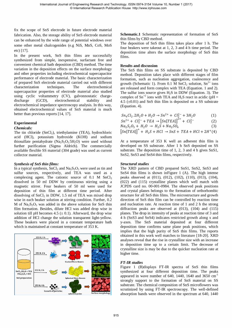
Synthesis of SnS thin films: In a typical synthesis, SnCl2 and Na2S2O3 were used as tin and
sulfur sources, respectively, and TEA was used as a
complexing agent. The cationic source of 0.1 M SnCl2
dissolved in 50 ml DDW by continuous stirring using a
magnetic stirrer. Four beakers of 50 ml were used for
deposition of thin film at different time period. After
dissolving of SnCl2 in DDW, 1.5 ml of TEA was mixed drop
wise in each beaker solution at stirring condition. Further, 0.2
M of Na2S2O3 was added in the above solution for SnS thin
film formation. Besides, dilute HCl was added drop wise in
solution till pH becomes 4.5 (± 0.1). Afterward, the drop wise
addition of HCl change the solution transparent light-yellow. These beakers were placed in a constant temperature bath
which is maintained at constant temperature of 353 K.
Schematic.1 Schematic representation of formation of SnS
thin films by CBD method.
The deposition of SnS thin films takes place after 1 h. The
four beakers were takeout at 1, 2, 3 and 4 h time period. The
deposition time alters the surface morphology of SnS thin films.
Results and discussion
The SnS thin films on SS substrate is deposited by CBD
method. Deposition takes place with different stages of film
formation, such as nucleation aggregation, coalescence and
growth (Schematic 1). From 0.1 M SnCl2 solution, Sn2+ ions
are released and form complex with TEA (Equation. 1 and 2).
The sulfur ions source gives H2S in DDW (Equation. 3). The
complex of Sn+2 ions with TEA and H2S react in acidic (pH =
4.5 (±0.01) and SnS thin film is deposited on a SS substrate
(Equation. 4).
𝑆𝑛4𝐶𝑙2 . 2𝐻2𝑂 + 𝐻2𝑂 → 𝑆𝑛2+ + 𝐶𝑙22− + 3𝐻2𝑂 (1)
𝑆𝑛2+ + 𝐶𝑙22− + 𝑇𝐸𝐴 → 𝑆𝑛 𝑇𝐸𝐴
2++ 𝐶𝑙2
2− (2) 𝑁𝑎2𝑆2𝑂3 + 𝐻2𝑂 → 𝐻2𝑆 + 𝑁𝑎2𝑆𝑂4 (3)
𝑆𝑛 𝑇𝐸𝐴 +
+ 𝐻2𝑆 + 𝐻𝐶𝑙 → 𝑆𝑛𝑆 + 𝑇𝐸𝐴 + 𝐻𝐶𝑙 + 2𝐻+(4)
At a temperature of 353 K well an adherent thin film is
developed on SS substrate. After 1 h SnS deposited on SS
substrate. The deposition time of 1, 2, 3 and 4 h gives SnS1,
SnS2, SnS3 and SnS4 thin films, respectively.
Structural studies The XRD pattern of CBD prepared SnS1, SnS2, SnS3 and
SnS4 thin films is shown inFigure 1 (A). The high intense
peaks observed at (011), (012), (102), (110), (013), (104),
(022) and (115) crystalline planes which well match with JCPDS card no. 00-001-0984. The observed peak positions
and crystal planes belongs to the formation of orthorhombic
structure for all SnS thin films. The microstructure and growth
direction of SnS thin film can be controlled by reaction time
and nucleation rate. At reaction time of 1 and 2 h the strong
diffraction peaks are observed at (013), (104) and (115)
planes. The drop in intensity of peaks at reaction time of 3 and
4 h (SnS3 and SnS4) indicates restricted growth along x and
y-axes. The SnS material deposited at four different
deposition time confirms same plane peak positions, which
implies that the high purity of SnS thin films. The reports obtained in this work well matches to literature [18-20]. XRD
analyses reveal that the rise in crystalline size with an increase
in deposition time up to a certain limit. The decrease of
crystalline size is may be due to the quicker nucleation rate at
higher time.
FT-IR studies
Figure 1 (B)displays FT-IR spectra of SnS thin films
synthesized at four different deposition time. The peaks
appeared in wave number of 640, 1440, 1640 and 3650 cm-1
strongly support to the formation of SnS material on SS
substrate. The chemical composition of SnS microflowers was scrutinized by using FT-IR spectroscopy. The well-defined
absorption bands were observed in the spectrum at 640, 1440
International Journal of Engineering Research and Technology. ISSN 0974-3154 Volume 10, Number 1 (2017) © International Research Publication House http://www.irphouse.com
915
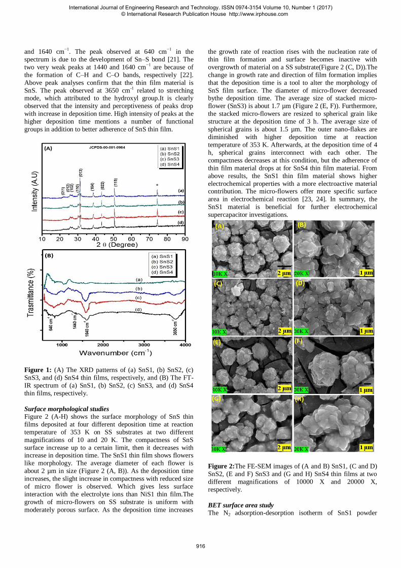
and 1640 cm−1. The peak observed at 640 cm−1 in the
spectrum is due to the development of Sn–S bond [21]. The
two very weak peaks at 1440 and 1640 cm−1 are because of
the formation of C–H and C–O bands, respectively [22].
Above peak analyses confirm that the thin film material is
SnS. The peak observed at 3650 cm-1 related to stretching mode, which attributed to the hydroxyl group.It is clearly
observed that the intensity and perceptiveness of peaks drop
with increase in deposition time. High intensity of peaks at the
higher deposition time mentions a number of functional
groups in addition to better adherence of SnS thin film.
Figure 1: (A) The XRD patterns of (a) SnS1, (b) SnS2, (c)
SnS3, and (d) SnS4 thin films, respectively, and (B) The FT-
IR spectrum of (a) SnS1, (b) SnS2, (c) SnS3, and (d) SnS4
thin films, respectively.
Surface morphological studies Figure 2 (A-H) shows the surface morphology of SnS thin
films deposited at four different deposition time at reaction
temperature of 353 K on SS substrates at two different
magnifications of 10 and 20 K. The compactness of SnS
surface increase up to a certain limit, then it decreases with increase in deposition time. The SnS1 thin film shows flowers
like morphology. The average diameter of each flower is
about 2 µm in size (Figure 2 (A, B)). As the deposition time
increases, the slight increase in compactness with reduced size
of micro flower is observed. Which gives less surface
interaction with the electrolyte ions than NiS1 thin film.The
growth of micro-flowers on SS substrate is uniform with
moderately porous surface. As the deposition time increases
the growth rate of reaction rises with the nucleation rate of
thin film formation and surface becomes inactive with
overgrowth of material on a SS substrate(Figure 2 (C, D)).The
change in growth rate and direction of film formation implies
that the deposition time is a tool to alter the morphology of
SnS film surface. The diameter of micro-flower decreased bythe deposition time. The average size of stacked micro-
flower (SnS3) is about 1.7 µm (Figure 2 (E, F)). Furthermore,
the stacked micro-flowers are resized to spherical grain like
structure at the deposition time of 3 h. The average size of
spherical grains is about 1.5 µm. The outer nano-flakes are
diminished with higher deposition time at reaction
temperature of 353 K. Afterwards, at the deposition time of 4
h, spherical grains interconnect with each other. The
compactness decreases at this condition, but the adherence of
thin film material drops at for SnS4 thin film material. From
above results, the SnS1 thin film material shows higher
electrochemical properties with a more electroactive material contribution. The micro-flowers offer more specific surface
area in electrochemical reaction [23, 24]. In summary, the
SnS1 material is beneficial for further electrochemical
supercapacitor investigations.
Figure 2:The FE-SEM images of (A and B) SnS1, (C and D)
SnS2, (E and F) SnS3 and (G and H) SnS4 thin films at two
different magnifications of 10000 X and 20000 X,
respectively.
BET surface area study The N2 adsorption-desorption isotherm of SnS1 powder
International Journal of Engineering Research and Technology. ISSN 0974-3154 Volume 10, Number 1 (2017) © International Research Publication House http://www.irphouse.com
916
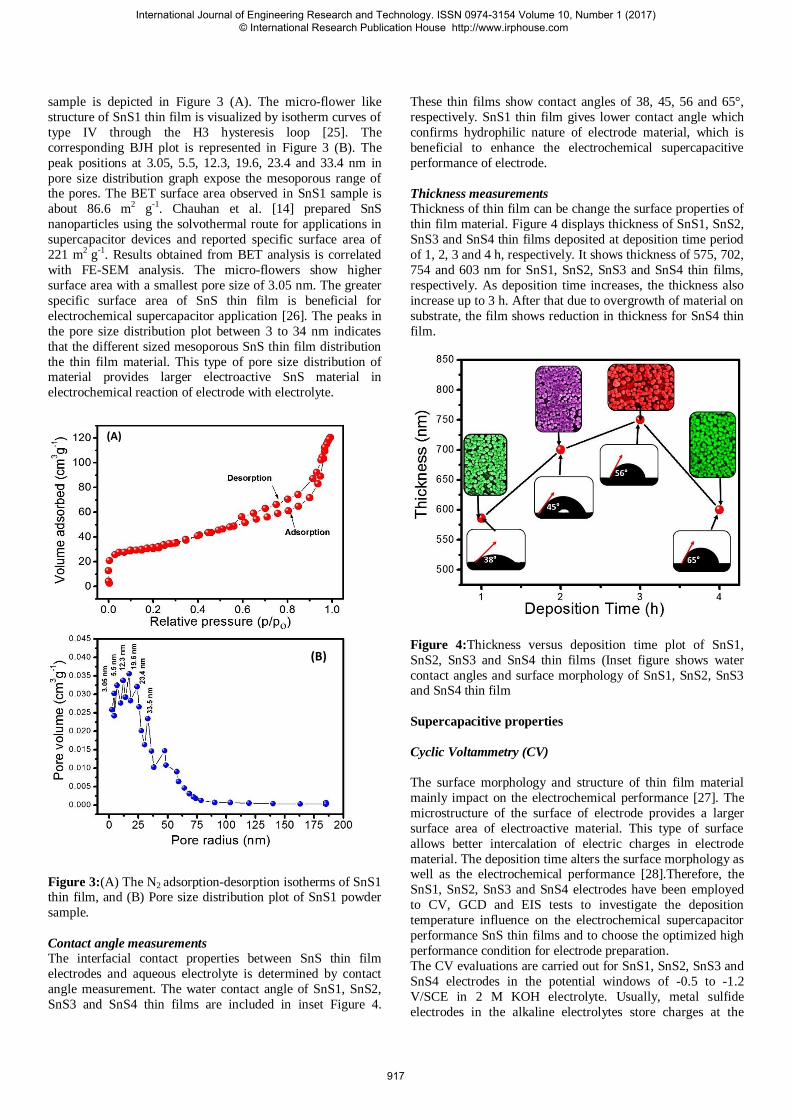
sample is depicted in Figure 3 (A). The micro-flower like
structure of SnS1 thin film is visualized by isotherm curves of
type IV through the H3 hysteresis loop [25]. The
corresponding BJH plot is represented in Figure 3 (B). The
peak positions at 3.05, 5.5, 12.3, 19.6, 23.4 and 33.4 nm in
pore size distribution graph expose the mesoporous range of the pores. The BET surface area observed in SnS1 sample is
about 86.6 m2 g-1. Chauhan et al. [14] prepared SnS
nanoparticles using the solvothermal route for applications in
supercapacitor devices and reported specific surface area of
221 m2 g-1. Results obtained from BET analysis is correlated
with FE-SEM analysis. The micro-flowers show higher
surface area with a smallest pore size of 3.05 nm. The greater
specific surface area of SnS thin film is beneficial for
electrochemical supercapacitor application [26]. The peaks in
the pore size distribution plot between 3 to 34 nm indicates
that the different sized mesoporous SnS thin film distribution
the thin film material. This type of pore size distribution of material provides larger electroactive SnS material in
electrochemical reaction of electrode with electrolyte.
Figure 3:(A) The N2 adsorption-desorption isotherms of SnS1 thin film, and (B) Pore size distribution plot of SnS1 powder
sample.
Contact angle measurements
The interfacial contact properties between SnS thin film
electrodes and aqueous electrolyte is determined by contact
angle measurement. The water contact angle of SnS1, SnS2,
SnS3 and SnS4 thin films are included in inset Figure 4.
These thin films show contact angles of 38, 45, 56 and 65°,
respectively. SnS1 thin film gives lower contact angle which
confirms hydrophilic nature of electrode material, which is
beneficial to enhance the electrochemical supercapacitive
performance of electrode.
Thickness measurements
Thickness of thin film can be change the surface properties of
thin film material. Figure 4 displays thickness of SnS1, SnS2,
SnS3 and SnS4 thin films deposited at deposition time period
of 1, 2, 3 and 4 h, respectively. It shows thickness of 575, 702,
754 and 603 nm for SnS1, SnS2, SnS3 and SnS4 thin films,
respectively. As deposition time increases, the thickness also
increase up to 3 h. After that due to overgrowth of material on
substrate, the film shows reduction in thickness for SnS4 thin
film.
Figure 4:Thickness versus deposition time plot of SnS1,
SnS2, SnS3 and SnS4 thin films (Inset figure shows water
contact angles and surface morphology of SnS1, SnS2, SnS3 and SnS4 thin film
Supercapacitive properties
Cyclic Voltammetry (CV)
The surface morphology and structure of thin film material
mainly impact on the electrochemical performance [27]. The
microstructure of the surface of electrode provides a larger
surface area of electroactive material. This type of surface
allows better intercalation of electric charges in electrode
material. The deposition time alters the surface morphology as well as the electrochemical performance [28].Therefore, the
SnS1, SnS2, SnS3 and SnS4 electrodes have been employed
to CV, GCD and EIS tests to investigate the deposition
temperature influence on the electrochemical supercapacitor
performance SnS thin films and to choose the optimized high
performance condition for electrode preparation.
The CV evaluations are carried out for SnS1, SnS2, SnS3 and
SnS4 electrodes in the potential windows of -0.5 to -1.2
V/SCE in 2 M KOH electrolyte. Usually, metal sulfide
electrodes in the alkaline electrolytes store charges at the
(A)
(B)
International Journal of Engineering Research and Technology. ISSN 0974-3154 Volume 10, Number 1 (2017) © International Research Publication House http://www.irphouse.com
917
interface of the electrode/electrolyte and in the bulk of
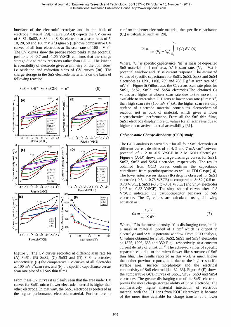
electrode material [29]. Figure 5(A-D) depicts the CV curves
of SnS1, SnS2, SnS3 and SnS4 electrode at a scan rates of 5,
10, 20, 50 and 100 mV s-1.Figure 5 (E)shows comparative CV
curves of all four electrodes at fix scan rate of 100 mV s-1.
The CV curves show the precise redox peaks at the potential positions of -0.7 and -1.05 V/SCE confirms that the charge
storage due to redox reactions rather than EDLC. The kinetic
irreversibility of electrode gives asymmetry on the both sides,
i.e oxidation and reduction sides of CV curves [30]. The
charge storage in the SnS electrode material is on the basis of
following reaction,
SnS + OH− ↔ SnSOH + e− (5)
Figure 5: The CV curves recorded at different scan rate for (A) SnS1, (B) SnS2, (C) SnS3 and (D) SnS4 electrodes,
respectively, (E) the comparative CV curves of all electrodes
at 100 mV s-1scan rate, and (F) the specific capacitance versus
scan rate plot of all SnS thin films.
From these CV curves it is clearly seen that the area under CV
curves for SnS1 micro-flower electrode material is higher than
other electrode. In that way, the SnS1 electrode is preferred as
the higher performance electrode material. Furthermore, to
confirm the better electrode material, the specific capacitance
(Cs) is calculated such as [28],
Cs =1
ms (V1 − V0) I (V) dV
V1
V0
(6)
Where, „Cs‟ is specific capacitance, „m‟ is mass of deposited SnS material on 1 cm2 area, „s‟ is scan rate, (V1 – V0) is
potential window and „I‟ is current response. The estimated
values of specific capacitance for SnS1, SnS2, SnS3 and SnS4
electrodes as 1290, 1100, 759 and 708 F g-1 at scan rate of 5
mV s-1. Figure 5(F)illustrates the Cs versus scan rate plots for
SnS1, SnS2, SnS3 and SnS4 electrodes.The obtained Cs
values are higher at alower scan rate due to the more time
available to intercalate OH- ions at lower scan rate (5 mV s-1)
than high scan rate (100 mV s-1).At the higher scan rate only
surface of electrode material contributes electrochemical
reaction not in bulk of material, which gives a lower
electrochemical performance. From all the SnS thin films, SnS1 electrode display more Cs values for all scan rates due to
higher electroactive material accessibility [31].
Galvonostatic Charge-discharge (GCD) study
The GCD analysis is carried out for all four SnS electrodes at
different current densities of 3, 4, 5 and 7 mA cm-2 between
potential of -1.2 to -0.5 V/SCE in 2 M KOH electrolyte.
Figure 6 (A-D) shows the charge-discharge curves for SnS1,
SnS2, SnS3 and SnS4 electrodes, respectively. The results
obtained from GCD curves confirms the capacitance
contributed from pseudocapacitor as well as EDLC type[14].
The lower interface resistance (IR) drop is observed for SnS1 electrode (-0.5 to -0.73 V/SCE) as compared to SnS2 (-0.5 to -
0.78 V/SCE), SnS3 (-0.5 to -0.81 V/SCE) and SnS4 electrodes
(-0.5 to -0.83 V/SCE). The slope shaped curves after -0.8
V/SCE indicated the pseudocapacitor behavior of SnS
electrode. The Cs values are calculated using following
equation as,
𝐶𝑠 =𝐼 × 𝑡
𝑚 × ∆𝑉 (7)
Where, „I‟ is the current density, „t‟ is discharging time, „m‟ is a mass of material loaded at 1 cm2 which is dipped in
electrolyte and „V‟ is potential window. From GCD analysis, Cs values obtained for SnS1, SnS2, SnS3 and SnS4 electrodes
as 1375, 1206, 688 and 350 F g-1, respectively, at a constant
current density of 3 mA cm-2. The achieved values of specific
capacitance is due to the micro-flower like structure of SnS
thin film. The results reported in this work is much higher
than other previous reports, it is due to the higher specific
surface area, surface morphology and the electrical
conductivity of SnS electrode[14, 32, 33]. Figure 6 (E) shows
the comparative GCD curves of SnS1, SnS2, SnS3 and SnS4
electrodes. The greater discharging rate of the SnS1 electrode
proves the more charge storage ability of SnS1 electrode. The comparatively higher material interaction of electrode
material with the OH- ions from KOH electrolyte is because
of the more time available for charge transfer at a lower
(A) (B)
(E)
(C) (D)
(F)
International Journal of Engineering Research and Technology. ISSN 0974-3154 Volume 10, Number 1 (2017) © International Research Publication House http://www.irphouse.com
918
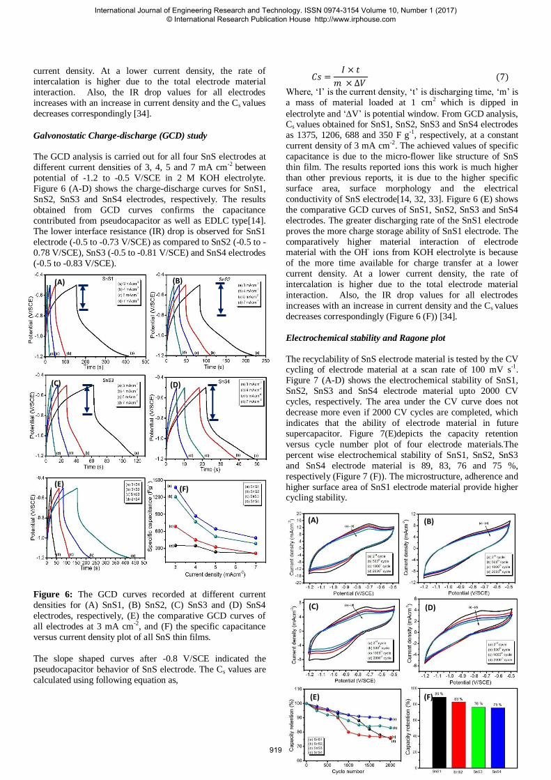
current density. At a lower current density, the rate of
intercalation is higher due to the total electrode material
interaction. Also, the IR drop values for all electrodes
increases with an increase in current density and the Cs values
decreases correspondingly [34].
Galvonostatic Charge-discharge (GCD) study
The GCD analysis is carried out for all four SnS electrodes at
different current densities of 3, 4, 5 and 7 mA cm-2 between
potential of -1.2 to -0.5 V/SCE in 2 M KOH electrolyte.
Figure 6 (A-D) shows the charge-discharge curves for SnS1,
SnS2, SnS3 and SnS4 electrodes, respectively. The results
obtained from GCD curves confirms the capacitance
contributed from pseudocapacitor as well as EDLC type[14].
The lower interface resistance (IR) drop is observed for SnS1
electrode (-0.5 to -0.73 V/SCE) as compared to SnS2 (-0.5 to -
0.78 V/SCE), SnS3 (-0.5 to -0.81 V/SCE) and SnS4 electrodes
(-0.5 to -0.83 V/SCE).
Figure 6: The GCD curves recorded at different current
densities for (A) SnS1, (B) SnS2, (C) SnS3 and (D) SnS4
electrodes, respectively, (E) the comparative GCD curves of
all electrodes at 3 mA cm-2, and (F) the specific capacitance
versus current density plot of all SnS thin films.
The slope shaped curves after -0.8 V/SCE indicated the
pseudocapacitor behavior of SnS electrode. The Cs values are
calculated using following equation as,
𝐶𝑠 =𝐼 × 𝑡
𝑚 × ∆𝑉 (7)
Where, „I‟ is the current density, „t‟ is discharging time, „m‟ is
a mass of material loaded at 1 cm2 which is dipped in
electrolyte and „V‟ is potential window. From GCD analysis, Cs values obtained for SnS1, SnS2, SnS3 and SnS4 electrodes
as 1375, 1206, 688 and 350 F g-1, respectively, at a constant
current density of 3 mA cm-2. The achieved values of specific
capacitance is due to the micro-flower like structure of SnS
thin film. The results reported ions this work is much higher
than other previous reports, it is due to the higher specific
surface area, surface morphology and the electrical
conductivity of SnS electrode[14, 32, 33]. Figure 6 (E) shows
the comparative GCD curves of SnS1, SnS2, SnS3 and SnS4
electrodes. The greater discharging rate of the SnS1 electrode
proves the more charge storage ability of SnS1 electrode. The
comparatively higher material interaction of electrode material with the OH- ions from KOH electrolyte is because
of the more time available for charge transfer at a lower
current density. At a lower current density, the rate of
intercalation is higher due to the total electrode material
interaction. Also, the IR drop values for all electrodes
increases with an increase in current density and the Cs values
decreases correspondingly (Figure 6 (F)) [34].
Electrochemical stability and Ragone plot
The recyclability of SnS electrode material is tested by the CV cycling of electrode material at a scan rate of 100 mV s-1.
Figure 7 (A-D) shows the electrochemical stability of SnS1,
SnS2, SnS3 and SnS4 electrode material upto 2000 CV
cycles, respectively. The area under the CV curve does not
decrease more even if 2000 CV cycles are completed, which
indicates that the ability of electrode material in future
supercapacitor. Figure 7(E)depicts the capacity retention
versus cycle number plot of four electrode materials.The
percent wise electrochemical stability of SnS1, SnS2, SnS3
and SnS4 electrode material is 89, 83, 76 and 75 %,
respectively (Figure 7 (F)). The microstructure, adherence and
higher surface area of SnS1 electrode material provide higher cycling stability.
(A)
(E)
(B)
(C) (D)
(F)
(A) (B)
(C) (D)
(E) (F)
International Journal of Engineering Research and Technology. ISSN 0974-3154 Volume 10, Number 1 (2017) © International Research Publication House http://www.irphouse.com
919
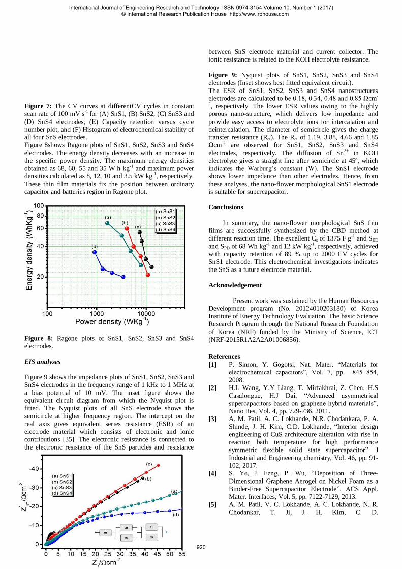
Figure 7: The CV curves at differentCV cycles in constant
scan rate of 100 mV s-1 for (A) SnS1, (B) SnS2, (C) SnS3 and
(D) SnS4 electrodes, (E) Capacity retention versus cycle
number plot, and (F) Histogram of electrochemical stability of
all four SnS electrodes.
Figure 8shows Ragone plots of SnS1, SnS2, SnS3 and SnS4
electrodes. The energy density decreases with an increase in
the specific power density. The maximum energy densities
obtained as 68, 60, 55 and 35 W h kg-1 and maximum power
densities calculated as 8, 12, 10 and 3.5 kW kg-1, respectively.
These thin film materials fix the position between ordinary capacitor and batteries region in Ragone plot.
Figure 8: Ragone plots of SnS1, SnS2, SnS3 and SnS4
electrodes.
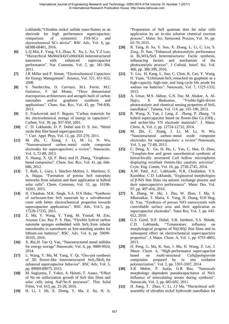
EIS analyses
Figure 9 shows the impedance plots of SnS1, SnS2, SnS3 and
SnS4 electrodes in the frequency range of 1 kHz to 1 MHz at
a bias potential of 10 mV. The inset figure shows the
equivalent circuit diagram from which the Nyquist plot is
fitted. The Nyquist plots of all SnS electrode shows the
semicircle at higher frequency region. The intercept on the
real axis gives equivalent series resistance (ESR) of an
electrode material which consists of electronic and ionic
contributions [35]. The electronic resistance is connected to
the electronic resistance of the SnS particles and resistance
between SnS electrode material and current collector. The
ionic resistance is related to the KOH electrolyte resistance.
Figure 9: Nyquist plots of SnS1, SnS2, SnS3 and SnS4
electrodes (Inset shows best fitted equivalent circuit).
The ESR of SnS1, SnS2, SnS3 and SnS4 nanostructures electrodes are calculated to be 0.18, 0.34, 0.48 and 0.85 Ωcm-
2, respectively. The lower ESR values owing to the highly
porous nano-structure, which delivers low impedance and
provide easy access to electrolyte ions for intercalation and
deintercalation. The diameter of semicircle gives the charge
transfer resistance (Rct). The Rct of 1.19, 3.88, 4.66 and 1.85
Ωcm-2 are observed for SnS1, SnS2, SnS3 and SnS4
electrodes, respectively. The diffusion of Sn2+ in KOH
electrolyte gives a straight line after semicircle at 45º, which
indicates the Warburg‟s constant (W). The SnS1 electrode
shows lower impedance than other electrodes. Hence, from
these analyses, the nano-flower morphological SnS1 electrode is suitable for supercapacitor.
Conclusions
In summary, the nano-flower morphological SnS thin
films are successfully synthesized by the CBD method at
different reaction time. The excellent Cs of 1375 F g-1 and SED
and SPD of 68 Wh kg-1 and 12 kW kg-1, respectively, achieved
with capacity retention of 89 % up to 2000 CV cycles for
SnS1 electrode. This electrochemical investigations indicates
the SnS as a future electrode material.
Acknowledgement
Present work was sustained by the Human Resources
Development program (No. 20124010203180) of Korea
Institute of Energy Technology Evaluation. The basic Science
Research Program through the National Research Foundation
of Korea (NRF) funded by the Ministry of Science, ICT
(NRF-2015R1A2A2A01006856).
References
[1] P. Simon, Y. Gogotsi, Nat. Mater. “Materials for
electrochemical capacitors”, Vol. 7, pp. 845−854,
2008.
[2] H.L Wang, Y.Y Liang, T. Mirfakhrai, Z. Chen, H.S
Casalongue, H.J Dai, “Advanced asymmetrical
supercapacitors based on graphene hybrid materials”,
Nano Res, Vol. 4, pp. 729-736, 2011.
[3] A. M. Patil, A. C. Lokhande, N.R. Chodankara, P. A.
Shinde, J. H. Kim, C.D. Lokhande, “Interior design
engineering of CuS architecture alteration with rise in
reaction bath temperature for high performance
symmetric flexible solid state supercapacitor”. J
Industrial and Engineering chemistry, Vol. 46, pp. 91-
102, 2017.
[4] S. Ye, J. Feng, P. Wu, “Deposition of Three-
Dimensional Graphene Aerogel on Nickel Foam as a
Binder-Free Supercapacitor Electrode”. ACS Appl.
Mater. Interfaces, Vol. 5, pp. 7122-7129, 2013.
[5] A. M. Patil, V. C. Lokhande, A. C. Lokhande, N. R. Chodankar, T. Ji, J. H. Kim, C. D.
International Journal of Engineering Research and Technology. ISSN 0974-3154 Volume 10, Number 1 (2017) © International Research Publication House http://www.irphouse.com
920
Lokhande,“Ultrathin nickel sulfide nano-flames as an
electrode for high performance supercapacitor;
comparison of symmetric FSS-SCs and
electrochemical SCs device”. RSC Adv, Vol. 6, pp.
68388-68401, 2016.
[6] L.Q Mai, F. Yang, Y.L Zhao, X. Xu, L. Xu, Y.Z Luo, “Hierarchical MnMoO(4)/CoMoO(4) heterostructured
nanowires with enhanced supercapacitor
performance”. Nat. Commun, Vol. 2, pp. 381-384,
2011.
[7] J.R Miller and P. Simon, “Electrochemical Capacitors
for Energy Management”. Science, Vol. 321, 651-652,
2008.
[8] S. Nardecchia, D. Carriazo, M.L Ferrer, M.C
Gutierrez, F. del Monte, “Three dimensional
macroporous architectures and aerogels built of carbon
nanotubes and/or graphene: synthesis and
applications”. Chem. Soc. Rev, Vol. 42, pp. 794-830, 2013.
[9] E. Frackowiak and F. Beguin, “Carbon materials for
the electrochemical storage of energy in capacitors”.
Carbon, Vol. 39, pp. 937-950, 2001.
[10] C. D. Lokhande, D. P. Dubal and O. S. Joo, “Metal
oxide thin film based supercapacitors
”. Curr. Appl. Phys, Vol. 11, pp. 255-270, 2011.
[11] M. Zhi, C. Xiang, J. Li, M. Li, N. Wu,
“Nanostructured carbon–metal oxide composite
electrodes for supercapacitors: a review”. Nanoscale,
Vol. 5, 72-88, 2013.
[12] X. Huang, X. Qi, F. Boey and H. Zhang, “Graphene-
based composites”. Chem. Soc. Rev, Vol. 41, pp. 666-
686, 2012.
[13] T. Rath, L. Gury, I. Sánchez-Molina, L. Martínez, S.
A. Haque, “Formation of porous SnS nanoplate
networks from solution and their application in hybrid
solar cells”. Chem. Commun, Vol. 51, pp. 10198-
10201, 2015.
[14] H. Chauhan, M.K. Singh, S.A. H.S Deka, “Synthesis
of surfactant-free SnS nanorods by a solvothermal
route with better electrochemical properties towards
supercapacitor applications”. RSC Adv, Vol.5, pp. 17228-17235, 2015.
[15] Z. Ma, Y. Wang, Y. Yang, M. Yousaf, M. Zou,
Anyuan Cao, Ray P. S. Han, “Flexible hybrid carbon
nanotube sponges embedded with SnS2 from tubular
nanosheaths to nanosheets as free-standing anodes for
lithium-ion batteries”. RSC. Adv, Vol. 6, pp. 30098-
30105, 2016.
[16] X. Rui,H. Tan, Q. Yan, “Nanostructured metal sulfides
for energy storage”.Nanoscale, Vol. 6, pp. 9889-9924,
2014.
[17] L. Wang, Y. Ma, M. Yang, Y. Qi, “One-pot synthesis of 3D flower-like heterostructured SnS2/MoS2 for
enhanced supercapacitor behavior”. RSC Adv, Vol. 5,
pp. 89069-89075, 2015.
[18] M. Sugiyama, T. Yokoi, A. Henmi, T. Asano, “Effect
of Na on sulfurization growth of SnS thin films and
solar cells using NaF/Sn-S precursor”. Thin Solid
Films, Vol. 615, pp. 25-28, 2016.
[19] H. Li, J. Jib, X. Zheng, Y. Ma, Z. Jin, H. Ji,
“Preparation of SnS quantum dots for solar cells
application by an in-situ solution chemical reaction
process”. Mater. Sci. Semicond. Process, Vol. 36, pp.
65-70, 2015.
[20] R. Tang, H. Su, Y. Sun, X. Zhang, L. Li, C. Liu, S.
Zeng, D. Sun, “Enhanced photocatalytic performance in Bi2WO6/SnS heterostructures: Facile synthesis,
influencing factors and mechanism of the
photocatalytic process”. J Colloid. Interf. Sci, Vol.
466, pp. 388-399, 2016.
[21] Y. Liu, H. Kang, L. Jiao, C. Chen, K. Cao, Y. Wang,
H. Yuan, “Exfoliated-SnS2 restacked on graphene as a
high-capacity, high-rate, and long-cycle life anode for
sodium ion batteries”. Nanoscale, Vol. 7, 1325-1332,
2015.
[22] A. Umar, M.S. Akhtar, G.N. Dar, M. Abaker, A. Al-
Hajry, S. Baskoutas, “Visible-light-driven
photocatalytic and chemical sensing properties of SnS2 nanoflakes”. Talanta, Vol. 114, pp. 183-190, 2013.
[23] R. Wang, X. Yan, J. Lang, Z. Zheng, P. Zhang, “A
hybrid supercapacitor based on flower-like Co (OH) 2
and urchin-like VN electrode materials”. J. Mater.
Chem. A, Vol. 2, pp. 12724-12732, 2014.
[24] M. Zhi, C. Xiang, J. Li, M. Li, N. Wu,
“Nanostructured carbon–metal oxide composite
electrodes for supercapacitors: a review”.Nanoscale,
Vol. 5, pp. 72-88, 2013.
[25] C. Deng, X. Ge, H. Hu, L. Yao, C. Han, D. Zhao,
“Template-free and green sonochemical synthesis of hierarchically structured CuS hollow microspheres
displaying excellent Fenton-like catalytic activities”.
Cryst. Eng. Comm, Vol. 16, pp. 2738-2745, 2014.
[26] A.M. Patil, A.C. Lokhande, N.R. Chodankar, V.S.
Kumbhar, C.D. Lokhande, “Engineered morphologies
of β-NiS thin films via anionic exchange process and
their supercapacitive performance”. Mater. Des. Vol.
97, pp. 407-416, 2016.
[27] X. Zhang, W. Shi, J. Zhu, W. Zhao, J. Ma, S.
Mhaisalkar, T. Maria, Y. Yang, H. Zhang, H.H Hng,
Q. Yan, “Synthesis of porous NiO nanocrystals with
controllable surface area and their application as supercapacitor electrodes”. Nano Res, Vol. 3, pp. 643-
652, 2010.
[28] G.S. Gund, D.P. Dubal, S.B. Jambure, S.S. Shinde,
C.D. Lokhande, “Temperature influence on
morphological progress of Ni(OH)2 thin films and its
subsequent effect on electrochemical supercapacitive
properties”. J. Mater. Chem. A, Vol. 1, pp. 4793-4803,
2013.
[29] H. Peng, G. Ma, K. Sun, J. Mu, H. Wang, Z. Lei, J.
Mater. Chem. A, “High-performance supercapacitor
based on multi-structural CuS@polypyrrole composites prepared by in situ oxidative
polymerization”. Vol. 2, pp. 3303-3307, 2014.
[30] S.K Meher, P. Justin, G.R Rao, “Nanoscale
morphology dependent pseudocapacitance of NiO:
Influence of intercalating anions during synthesis”.
Nanoscale, Vol. 3, pp. 683-692, 2011.
[31] H. Jiang, T. Zhao, C. Li, J.J Ma, “Hierarchical self-
assembly of ultrathin nickel hydroxide nanoflakes for
International Journal of Engineering Research and Technology. ISSN 0974-3154 Volume 10, Number 1 (2017) © International Research Publication House http://www.irphouse.com
921
high-performance supercapacitors”. Mater. Chem,
Vol. 21, pp. 3818-3823, 2011.
[32] Y. Li, H. Xie and J. Tu, Mater. Lett, “Nanostructured
SnS/carbon composite for supercapacitor”. Vol. 63,
pp. 1785-1787, 2009.
[33] S. Sohila, M. Rajalakshmi, C. Muthamizhchelvan, S. Kalavathi, C. Ghosh, R. Divakar, C. N.
Venkiteswaran, N. G. Muralidharan, A. K. Arora, E.
Mohandas, “Synthesis and characterization of SnS
nanosheets through simple chemical route”. Mater.
Lett, Vol. 65, pp. 1148-1150, 2011.
[34] S. Vijayakumar, S. Nagamuthu, G. Muralidharan,
ACS Appl. Mater. Interfaces, 5 (2013) 2188.
International Journal of Engineering Research and Technology. ISSN 0974-3154 Volume 10, Number 1 (2017) © International Research Publication House http://www.irphouse.com
922