Electrochemical Modification & Photoelectronic Properties ... · Electrochemical Modification &...
106
Electrochemical Modification & Photoelectronic Properties of Carbon Nanotubes TH ` ESE N ◦ 3201 (2005) PR ´ ESENT ´ EE A LA FACULTE SCIENCES DE BASE Institut de physique des nanostructures SECTION DE PHYSIQUE ´ ECOLE POLYTECHNIQUE F ´ ED ´ ERALE DE LAUSANNE POUR L’OBTENTION DU GRADE DE DOCTEUR ` ES SCIENCES PAR Kannan Balasubramanian M. Sc. / Diplom Ingenieur, Universit¨at Gesamthochschule Kassel, Allemagne et de nationalit´ e indienne accept´ ee sur proposition du jury: Prof. K. Kern, directeur de th` ese Dr. M. Burghard, rapporteur Prof. L. Forr´o, rapporteur Prof. L. Schlapbach, rapporteur Lausanne, EPFL 2005
Transcript of Electrochemical Modification & Photoelectronic Properties ... · Electrochemical Modification &...
Electrochemical Modification &
Photoelectronic Properties of
Carbon Nanotubes
THESE N 3201 (2005)
PRESENTEE A LA FACULTE SCIENCES DE BASE
Institut de physique des nanostructures
SECTION DE PHYSIQUE
ECOLE POLYTECHNIQUE FEDERALE DE LAUSANNE
POUR L’OBTENTION DU GRADE DE DOCTEUR ES SCIENCES
PAR
Kannan Balasubramanian
M. Sc. / Diplom Ingenieur, Universitat Gesamthochschule Kassel, Allemagne
et de nationalite indienne
acceptee sur proposition du jury:
Prof. K. Kern, directeur de these
Dr. M. Burghard, rapporteur
Prof. L. Forro, rapporteur
Prof. L. Schlapbach, rapporteur
Lausanne, EPFL
2005

Abstract
This thesis reports on the investigations performed on electrochemical functionaliza-
tion and photoelectronic transport properties of individual single-wall carbon nanotubes
(SWCNTs).
The first part of the thesis is concerned with the controlled modification of indi-
vidual nanotubes through electrochemistry. The electrochemical modification has been
performed using reductive and oxidative coupling schemes, resulting in thin molecular
coatings around the SWCNTs. The former scheme is based on a reactive diazonium salt,
while the latter involved a substituted aromatic amine. The characterization methods
included electrical transport measurements and confocal Raman spectroscopy, both of
which can address selected single SWCNTs or bundles. These studies were performed
separately on metallic and semiconducting nanotubes, in both cases comparing the effect
of the oxidative and reductive coupling schemes. While the oxidative scheme was found
to yield non-covalently attached layers on the nanotubes, the reductive modification led
to covalently grafted phenyl groups.
The reductive coupling scheme was utilized to address a fundamental problem in
the creation of nanotube field-effect transistors (FETs). The fabrication of FETs using
carbon nanotubes has been impeded as all current production procedures yield a mix-
ture of metallic and semiconducting tubes. In this work, a generic approach employing
electrochemistry for selective covalent modification of metallic nanotubes was devised,
resulting in exclusive electrical transport through the unmodified semiconducting tubes.
Towards this goal, the semiconducting tubes were rendered non-conductive by applica-
tion of an appropriate gate voltage prior to the electrochemical modification. The FETs
fabricated in this manner were found to display favourable hole mobilities and a high
ratio approaching 106 between the current in the ON and OFF state.
The second part of the thesis deals with electronic transport through individual
carbon nanotubes under local photo–illumination. The source of excitation was a
diffraction–limited laser spot (diameter ≈ λexc/2) generated by a confocal scanning
optical microscope. Using this setup, photoconductivity in individual semiconducting
i
ii ABSTRACT
SWCNTs was investigated in detail. The magnitude of the photocurrent was found
to increase linearly with the laser intensity, and was maximum for parallel orientation
between the light polarization and the tube axis. Larger currents were obtained upon
illuminating the tubes at 514.5 nm in comparison to those at 647.1 nm, consistent with
the investigated semiconducting tubes having a resonant absorption energy at the former
wavelength.
Furthermore, due to the relatively small diameter of the laser spot, the photore-
sponse could be measured as a function of position, which allowed the acquisition of
photoelectronic transport (PET) images of individual nanotubes. During the course
of this work, the PET imaging technique was developed into a useful tool to monitor
local electronic structure effects, including the observation of Schottky barriers at the
contacts with semiconducting SWCNTs. Subsequently, metallic SWCNTs were investi-
gated by recording PET images. The locally induced photocurrents directly reflect the
existence of built-in electric fields associated with the presence of depletion layers at
the contacts or structural defects along the tubes. These observations have strong im-
plications on the realisation of high-performance electrical devices incorporating carbon
nanotubes, which critically depends on the minimisation of charge transport barriers
along the tubes and at the contacts.
Resume
Cette these rapporte les investigations effectuees sur la fonctionnalisation
electrochimique et les proprietes de transport photoelectrique de nanotubes de
carbone individuels a mono-parois (SWCNTs).
La premiere partie de la these traite la modification controlee de nanotubes indi-
viduels par l’electrochimie. La modification electrochimique a ete effectuee en utilisant
des reactions de couplage par reduction et par oxydation, donnant lieu a une fine couche
moleculaire autour des SWCNTs. La reaction de reduction est faite a partir d’un sel
reactif de diazonium, tandis qu’une amine aromatique substituee est utilisee pour la
reaction d’oxydation. Les methodes de caracterisation ont inclu des mesures de trans-
port electriques et de spectroscopie confocale de Raman. Dans les deux cas, il a ete
possible de choisir d’effectuer selectivement les mesures sur un unique ou bien un pa-
quet de SWCNTs. Ces etudes ont ete realisees separement sur des nanotubes metalliques
et semi-conducteurs en comparant l’effet des reactions de couplage par oxydation et par
reduction. Tandis que la reaction d’oxydation a cree des couches attachees de maniere
non covalentes aux nanotubes, la modification par reduction a mene a des groupes
phenyles lies de facon covalente aux nanotubes.
La reaction de couplage par reduction a ete utilisee pour resoudre un probleme
fondamental dans la creation des transistors a effet de champ base sur les nanotubes
(FETs). La fabrication des FETs a partir de nanotubes de carbone s’est heurtee au fait
des procedures courantes de production qui donnent lieu exclusivement a un melange
de tubes metalliques et semi-conducteurs. Dans ce travail, une approche generique
utilisant l’electrochimie a ete concue pour modifier par oxydation de facon selective les
seuls nanotubes metalliques, ayant pour resultat le transport electrique exclusif par les
tubes semi-conducteurs non modifies. Pour cette realisation, les tubes semi-conducteurs
ont ete rendus non-conducteurs par l’application d’une tension gate appropriee avant la
modification electrochimique. Les FETs ainsi fabriques ont montre des mobilites de trou
favorables et un rapport eleve approchant 106 entre le courant dans l’etat de marche et
le courant dans l’etat d’arret.
iii
iv RESUME
La deuxieme partie de la these traite le transport electrique par des nanotubes in-
dividuels de carbone sous l’effet d’une photo-illumination locale. La source d’excitation
fut un faisceau laser a diffraction limitee (diametre ≈ λexc/2) produite par un micro-
scope optique confocal a balayage. En utilisant cette installation, la photoconductivite
de SWCNTs semi-conducteurs individuels a ete etudiee en detail. L’importance du
courant photoelectrique montre une augmentation lineaire avec l’intensite du laser, et
devient maximale pour une orientation parallele entre la polarisation de la lumiere et
l’axe du tube. De plus grands courants ont ete obtenus lorsque les tubes ont ete illumine
par une lumiere de 514,5 nm de longueur d’onde au lieu de 647,1 nm. Ce resultat est
coherent avec l’energie resonnante d’absorption a 514,5 nm de longueur d’onde des tubes
semi-conducteurs etudies.
En outre, en raison du diametre relativement petit du faisceau laser, la reponse
photoelectrique peut etre mesuree en fonction de la position du faisceau sur le tube,
ce qui a permis l’obtention d’images du transport photoelectrique (PET) de nanotubes
individuels. Au cours de ce travail, la technique images PET a ete developpee afin de
pouvoir surveiller les effets de structure electronique locale, y compris l’observation de
barrieres de Schottky au niveau des contacts avec les SWCNTs semi-conducteurs. Par la
suite, les images PET des SWCNTs metalliques ont ete etudiees avec la meme technique.
Les courants photoelectriques localement induits refletent directement la pre-existence
de champs electriques lies a la presence de region a densite de charge plus faible au
niveau des contacts ainsi qu’a l’effet des defauts structuraux le long des tubes. Ces
observations ont d’importantes implications pour la realisation de dispositifs electriques
a rendement eleve incorporant des nanotubes de carbone puisqu’un element essentiel a
leur realisation est la minimisation des barrieres de transport de charge le long des tubes
et au niveau des contacts.
Contents
Abstract i
Resume iii
1 Introduction 1
2 Carbon Nanotubes: Fundamentals 5
2.1 Physical structure . . . . . . . . . . . . . . . . . . . . . . . . . . . . . . . 6
2.2 Electronic structure . . . . . . . . . . . . . . . . . . . . . . . . . . . . . . 7
2.3 Optical absorption and photoluminescence . . . . . . . . . . . . . . . . . 10
2.4 Phonon structure . . . . . . . . . . . . . . . . . . . . . . . . . . . . . . . 12
2.4.1 Resonant Raman scattering . . . . . . . . . . . . . . . . . . . . . 12
2.4.2 Phonon modes and Raman spectra . . . . . . . . . . . . . . . . . 12
2.5 Chemically functionalized carbon nanotubes . . . . . . . . . . . . . . . . 15
2.5.1 Chemical nature of carbon nanotubes . . . . . . . . . . . . . . . . 16
2.5.2 Thermally activated chemistry . . . . . . . . . . . . . . . . . . . . 17
2.5.3 Electrochemical modification . . . . . . . . . . . . . . . . . . . . . 20
2.5.4 Photochemical functionalization . . . . . . . . . . . . . . . . . . . 22
3 Experimental 25
3.1 Sample preparation . . . . . . . . . . . . . . . . . . . . . . . . . . . . . . 25
3.2 Electronic transport measurements . . . . . . . . . . . . . . . . . . . . . 29
3.3 Confocal laser scanning microscopy . . . . . . . . . . . . . . . . . . . . . 34
4 Electrochemical Modification 41
4.1 Instrumentation . . . . . . . . . . . . . . . . . . . . . . . . . . . . . . . . 42
4.2 Electrochemical modification . . . . . . . . . . . . . . . . . . . . . . . . . 43
4.2.1 Coupling schemes . . . . . . . . . . . . . . . . . . . . . . . . . . . 43
4.2.2 Oxidative electrochemical modification . . . . . . . . . . . . . . . 44
4.2.3 Reductive electrochemical modification . . . . . . . . . . . . . . . 47
v
vi CONTENTS
4.2.4 Discussion . . . . . . . . . . . . . . . . . . . . . . . . . . . . . . . 48
4.3 Field-effect transistors through selective ECM . . . . . . . . . . . . . . . 50
4.3.1 Motivation - Separation techniques . . . . . . . . . . . . . . . . . 50
4.3.2 Selective ECM on bundles of SWCNTs . . . . . . . . . . . . . . . 51
4.3.3 Selective ECM applied to nanotube networks . . . . . . . . . . . . 56
4.4 Outlook . . . . . . . . . . . . . . . . . . . . . . . . . . . . . . . . . . . . 57
5 Photoelectronic transport 59
5.1 Photoelectronic transport – Background . . . . . . . . . . . . . . . . . . 59
5.2 Instrumentation . . . . . . . . . . . . . . . . . . . . . . . . . . . . . . . . 61
5.2.1 Inverted Zeiss confocal microscope . . . . . . . . . . . . . . . . . 62
5.2.2 Leica confocal microscope . . . . . . . . . . . . . . . . . . . . . . 63
5.3 Photoelectronic transport in semiconducting SWCNTs . . . . . . . . . . 64
5.3.1 Photoconductivity in s-SWCNTs . . . . . . . . . . . . . . . . . . 64
5.3.2 Effect of Schottky barriers . . . . . . . . . . . . . . . . . . . . . . 68
5.4 Photoelectronic transport in metallic SWCNTs . . . . . . . . . . . . . . 73
5.4.1 Schottky barriers in m-SWCNT devices . . . . . . . . . . . . . . . 73
5.4.2 Structural inhomogeneities in m-SWCNTs . . . . . . . . . . . . . 77
5.5 Outlook . . . . . . . . . . . . . . . . . . . . . . . . . . . . . . . . . . . . 79
6 Summary and Conclusion 81
Bibliography 85
Publications 93
Curriculum vitae 95
Acknowledgements 97
Chapter 1
Introduction
Since the days of the earliest known human civilization, mankind is motivated with a
continuous drive for development. First came the invention of the wheel, followed by
the ability to use metals and going through a series of Ages there came the Industrial
Revolution in the 18th century A.D. This was ensued by the semiconductor era in the
20th century with the invention of the transistor and integrated circuits. This series of
developments has brought in comfort and luxury that one could not have imagined of
at the dawn of civilization. Apart from these technological developments, one tends to
forget the progress that has been made in the development of basic services to humanity.
This concerns the advances in medicine that has occured since the Stone Age. We have
come a long way from using herbs available in the jungle to drugs that are specifically
designed for a particular purpose. The technological advances have always walked hand-
in-hand with medicinal research to achieve capabilities as complex as transplanting a
heart of one person by that of another.
The human urge to continue along this trend has led to the emergence of a new field
towards the end of the last century, namely nanotechnology. This involves – among
other objectives – bringing the technological advances one step further by reducing
the size of electronic devices by around three orders of magnitude. Carbon Nanotubes
(CNTs) are an important element in this rapidly emerging field due to their miniscule
diameters of a few nm combined with their promise to function as efficient components
of electronic devices. Apart from use in nano-scale devices, due to their biocompatibility
arising from their carbonaceous nature, they are being considered for drug delivery and
for basic research in medicine. Thus they possess the unique aspect of the ability to
merge technological advances with medicinal applications and hence have become one
of the most intensively investigated materials. This is reflected, for instance, by the
continuously increasing number of publications, which exceeded three thousand in the
1
2 CHAPTER 1. INTRODUCTION
year 2003 [1].
CNTs can be visualized as being composed of concentric cylinders of a single atomic
layer of graphite (graphene sheet). They are classified as single-wall CNTs (SWCNTs)
comprising of just a single shell and multi-wall CNTs (MWCNTs) comprising of at
least two shells of the graphene layer. The work in this thesis focusses only on SWC-
NTs. The extraordinary interest in the study of SWCNTs stems from their outstanding
structural, mechanical and electronic properties. SWCNTs are ideal candidates as 1D
single molecule systems and are intriguing for fundamental studies. Mechanically they
possess extraordinarily high tensile strength, which outreaches that of a steel wire of
corresponding thickness by around one order of magnitude. This combined with their
low density (one-sixth that of steel) makes them highly suited for composites. Elec-
trically, they can be found as both metallic and semiconducting tubes. Due to their
microscopic dimensions, they have become one of the most successful materials for the
fabrication of molecular-scale electronic devices. These aspects make them highly valu-
able for applications in electronics, scanning probe microscopy, chemical and biological
sensing, reinforced composite materials, and many more. While some of the proposed
applications remain still a far-off dream, others are close to a technical realization.
Recent advances in the development of reliable methods for the chemical function-
alization of nanotubes provide an additional impetus towards extending the scope of
their application spectrum. Through appropriate modification schemes, the surface of
the SWCNTs can be imparted with a desired functionality, such as high water solubil-
ity, good chemical sensitivity or large photoresponsiveness. Although such possibilities
sound indeed promising, reports on controlled chemical modification of SWCNTs are
only starting to appear. Due to their curvature introduced by their cylindrical na-
ture, they are more reactive than graphite [2]. The chemical modification schemes that
are being devised can be classified into three categories [3] namely thermally activated
chemistry, electrochemical modification (ECM) and photochemistry. While thermally
activated functionalization procedures have been demonstrated for the attachment of a
variety of functional groups onto SWCNTs [4, 5], photochemical modification of SWC-
NTs is still in its infancy. Electrochemistry is an elegant approach that allows for an
effective control over the extent and type of modification.
Work on chemical functionalization of SWCNTs has been until now mostly per-
formed on bulk SWCNT material. However, for a detailed understanding of the mech-
anism of chemical modification and the resulting properties, molecular-scale studies at
a single object level are essential. This thesis describes a first step in this direction,
wherein individually addressable SWCNTs have been electrochemically modified and
3
characterized. The characterization has been performed by electronic transport and
confocal Raman spectroscopic measurements on the same individual SWCNTs before
and after the electrochemical modification. These studies were undertaken separately
for individual metallic and semiconducting SWCNTs.
The ECM approach has enabled a novel route to field-effect transistors (FETs). Pris-
tine SWCNTs are themselves prospective components of nanoscale electronic devices [6].
For instance, FETs have been successfully fabricated from single semiconducting nan-
otubes [7,8]. The overall performance of SWCNT-FETs has been reported to be superior
to that of state-of-the-art silicon based MOSFETs, as reflected in the values of the drive
current and transconductance being higher by a factor of four [9]. Moreover, devices
implementing CVD-grown SWCNTs have shown extremely high hole mobilities [10] of
up to 9000 cm2/Vs at room–temperature. With palladium as the electrode material,
Schottky barrier-free ballistic FETs [11] have recently been realized, exhibiting high
drive currents, good transconductance and switching ratios of 106.
However, the use of SWCNTs in the electronics industry is largely limited due to
the occurence of a mixture of both metallic and semiconducting SWCNTs. Solution-
based techniques for separation of metallic SWCNTs (m-SWCNTs) from semiconduct-
ing ones (s-SWCNTs) do not provide a quantitative separation [12–15]. Another ap-
proach is based on the fabrication of the FET device with a mixture of m-SWCNTs
and s-SWCNTs followed by selective burning of the m-SWCNTs through high voltage
ramps [16]. The procedure developed in this thesis extends the scope of the latter
technique by using the gate voltage to switch off the s-SWCNTs in an ensemble and se-
lectively modify the m-SWCNTs in a covalent manner. Since the modified m-SWCNTs
do not contribute to the transport due to their high resistance, this results in a purely
semiconducting network that can function as an FET.
Apart from their exquisite electronic properties, the optical properties of SWCNTs
have also attracted great attention. The direct band gap in semiconducting nanotubes
combined with their one dimensional electronic structure opens up possibilities for their
use as components of future nanoscale optoelectronic devices. The strong 1D con-
finement in SWCNTs should lead to large Coulombic coupling between photoexcited
electrons (e) and holes (h) to create strongly bound excitons [17]. Correspondingly, the
absorption intensity should be enhanced because of the increased e–h overlap. Appli-
cation of a drain-source bias leads to a flow of the photoexcited carriers resulting in
the generation of a photocurrent in s-SWCNTs. Photoinduced current modulation was
first observed in nanotube films [18]. Illumination of ensembles of very small diameter
nanotubes formed within a zeolite pores produced a slight polarization-dependent cur-
4 CHAPTER 1. INTRODUCTION
rent enhancement [19]. Filaments of nanotube bundles between two electrodes showed
current generation upon light illumination, which was attributed to either a thermoelec-
tric or a photovoltaic effect [20]. Although these experiments indicated that ensembles
of carbon nanotubes do respond electronically to light, it is highly desirable to under-
stand this interaction in detail and on a single molecule basis. Using an infrared laser,
photoconductivity from a single s-SWCNT incorporated as the channel of an ambipolar
FET could be observed [21]. However, in this and all the other previous experiments, a
laser spot with a diameter of at least a few µm was used for illumination of the whole
sample to observe the photoelectronic effects. This does not allow the investigation
of transport barriers at the contacts and other local inhomogeneities along the tube.
This thesis describes the first experimental setup of its kind that combines a confocal
laser scanning Raman microscope with electronic transport measurements to observe
localized photoelectronic transport through individual SWCNTs.
The thesis is organized as follows. The second chapter gives an overview of the
fundamental properties of carbon nanotubes. In the third chapter, the experimental
techniques used in this work are outlined. Electrochemical modification of individual
carbon nanotubes and its ensuing application towards fabrication of FETs is presented
in the fourth chapter. Chapter 5 is devoted to the investigations performed on photoelec-
tronic transport properties of individual metallic and semiconducting SWCNTs. The
thesis finally ends with a conclusion including a summary of the important achievements
attained in this work.
Chapter 2
Carbon Nanotubes: Fundamentals
Carbon nanotubes (CNTs) are cylinder-shaped macromolecules with radius as small
as few nm, which can be grown up to 20 cm in length [22]. The walls of these tubes
are made up of a hexagonal lattice of carbon atoms analogous to the atomic plane of
graphite. They are capped at their ends by a half of a fullerene-like molecule. In the
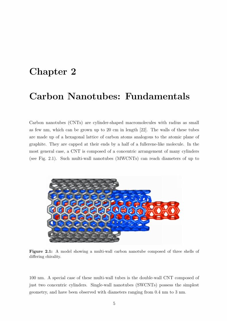
most general case, a CNT is composed of a concentric arrangement of many cylinders
(see Fig. 2.1). Such multi-wall nanotubes (MWCNTs) can reach diameters of up to
Figure 2.1: A model showing a multi-wall carbon nanotube composed of three shells ofdiffering chirality.
100 nm. A special case of these multi-wall tubes is the double-wall CNT composed of
just two concentric cylinders. Single-wall nanotubes (SWCNTs) possess the simplest
geometry, and have been observed with diameters ranging from 0.4 nm to 3 nm.
5
6 CHAPTER 2. CARBON NANOTUBES: FUNDAMENTALS
2.1 Physical structure
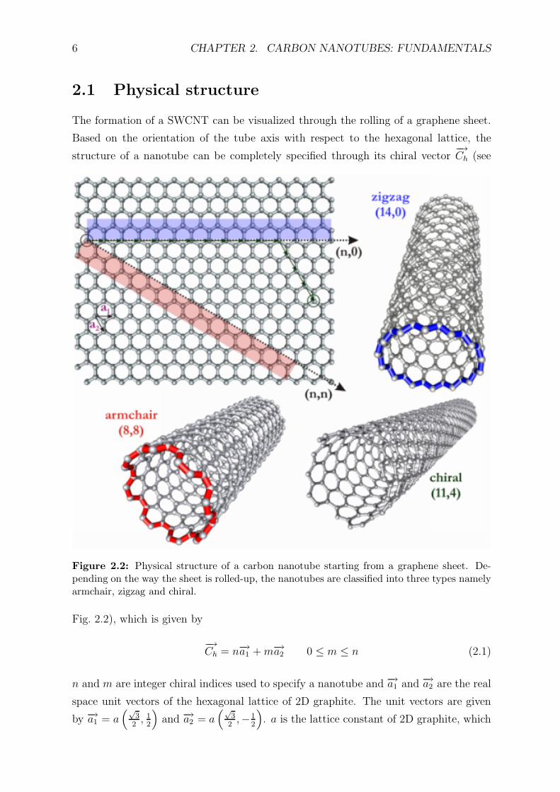
The formation of a SWCNT can be visualized through the rolling of a graphene sheet.
Based on the orientation of the tube axis with respect to the hexagonal lattice, the
structure of a nanotube can be completely specified through its chiral vector−→Ch (see
Figure 2.2: Physical structure of a carbon nanotube starting from a graphene sheet. De-pending on the way the sheet is rolled-up, the nanotubes are classified into three types namelyarmchair, zigzag and chiral.
Fig. 2.2), which is given by
−→Ch = n−→a1 + m−→a2 0 ≤ m ≤ n (2.1)
n and m are integer chiral indices used to specify a nanotube and −→a1 and −→a2 are the real
space unit vectors of the hexagonal lattice of 2D graphite. The unit vectors are given
by −→a1 = a(√
32
, 12
)
and −→a2 = a(√
32
,−12
)
. a is the lattice constant of 2D graphite, which
2.2. ELECTRONIC STRUCTURE 7
is 2.46 Angstrom. The diameter of an (m, n) SWCNT is then given by d =∣
∣
∣
−→Ch
∣
∣
∣/π.
The classification of the nanotubes as armchair (n = m) or zigzag (m = 0) has its
origin from the geometric arrangement of the carbon atoms at the seam of the cylinders.
While both these types of tubes possess mirror symmetry, nanotubes with m 6= n are
chiral. The latter kind of tubes exists as two enantiomers with right- and left-handed
helicity. Historically the multi-wall nanotubes were the first to be discovered (1991) [23],
followed by their single-wall [24, 25] counterparts (1993).
2.2 Electronic structure
Since the earliest stages of the emergence of carbon nanotubes, their electrical properties
have attracted particular interest. The electronic properties of SWCNTs were first
calculated using a tight-binding model by applying the zone-folding approach [6], which
derives the electronic structure of nanotubes directly from that of graphite. In graphite,
the electrons in the π-(valence) band and the π∗-(conduction) band are the ones that
are relevant for the electronic transport and other solid state properties. Despite the
simplicity of the tight-binding approach, it provides important insight into the electronic
strucutre of the π- and π∗-bands of graphite.
To arrive at the electronic structure of carbon nanotubes, one starts with the energy
dispersion relation for 2D graphite, which is given by [6]
Eg (kx, ky) = ±t
1 + 4 cos
(√3kxa
2
)
cos
(
kya
2
)
+ 4 cos2
(
kya
2
)
1/2
(2.2)
where kx and ky are the x and y components of the wave vector in the reciprocal lattice
and t is the tight-binding transfer integral signifying the interaction between nearest
neighbour carbon atoms. For the purpose of calulations t takes a value of −2.9 eV.
However, from experiments that are used to measure the electronic structure, differing
values around −3 eV have been found. The energy dispersion relations given by (2.2)
are plotted in Fig. 2.3. The upper half of the energy dispersion curves in Fig. 2.3(a)
describes the π∗-(conduction) bands while the lower half the π-(valence) band. The
π∗ and the π bands are degenerate at the K point through which the Fermi energy
passes. The shaded hexagon corresponds to the first Brillouin zone. In Fig. 2.3(b) a
color-coded projection of the dispersion relations is depicted, with the marked hexagon
again describing the first Brillouin zone. The high symmetry points are marked by K,
Γ and M.
The electronic structure of a SWCNT can now be directly obtained from that of

8 CHAPTER 2. CARBON NANOTUBES: FUNDAMENTALS
Figure 2.3: Dispersion relations for a 2D graphene sheet, obtained by the tight binding model:(a) 3D plot of the energy dispersion relations for 2D graphite given by (2.2). (b) Color-codedplot of the same function with blue regions having values close to minima and the red regionshaving values close to maxima. The vertices of the hexagon correspond to those points wherethe π and π∗ bands are degenerate.
two-dimensional graphite. By using periodic boundary conditions along the circumfer-
ential direction denoted by the chiral vectior−→Ch, the wave vector associated with the
circumferential direction gets quantized, while the translational wave vector that runs
along an infinitely long nanotube remains continuous. As a result of this, the energy
bands consist of a set of one-dimensional energy dispersion relations, which are cross
sections of those for 2D graphite. When performing this procedure, if one of the cutting
lines passes through the K point of the 2D Brillouin zone, the one-dimensional energy
bands will have a zero energy gap and the density of states at the Fermi level will be
finite. Such nanotubes are metallic. Armchair tubes (m = n) and zigzag and chiral
tubes with m − n being a multiple of 3 belong to this category. On the other hand,
if the intersecting lines does not pass through a K point, then the carbon nanotube
is semiconducting with a finite energy gap between the valence and conduction bands.
Zigzag and chiral tubes with m−n not being a multiple of 3 are semiconducting [26,27].
Explicit expressions for the energy dispersion relations for SWCNTs can be obtained
by imposing appropriate boundary conditions into the 2D dispersion relations of (2.2),
depending on the type of tube under consideration. The relations for the armchair and
zigzag tubes are the simplest to obtain in this manner. The one-dimensional energy
dispersion relations for armchair SWCNTs with−→Ch = (n, n) is given by [28]
Eq(k) = ±t
1 ± 4 cos(qπ
n
)
cos
(
ka
2
)
+ 4 cos2
(
ka
2
)1/2
(
−π
a< k <
π
a
)
, (q = 1, · · · , 2n) (2.3)

2.2. ELECTRONIC STRUCTURE 9
Thus all armchair tubes possess 4n energy subbands with 2n conduction and 2n valence
bands and of the 2n bands, two are nondegenerate and (n−1) are doubly degenerate. In
a similar manner, the energy dispersion relations for zigzag nanotubes with−→Ch = (n, 0)
have been derived as [28]
Eq(k) = ± t
1 ± 4 cos(qπ
n
)
cos
(√3ka
2
)
+ 4 cos2(qπ
n
)
1/2
(
−π√3a
< k <π√3a
)
, (q = 1, · · · , 2n) (2.4)
Figure 2.4: Calculated energy dispersion relations for SWCNTs: (a) (15,0) metallic SWCNT.(b) (14,0) semiconducting SWCNT.
Figures 2.4(a) and (b) show respectively the energy dispersion relations for a (15,0)
SWCNT and a (14,0) SWCNT. There is no energy gap at k = 0 for the (15,0) metallic
nanotube, while the (14,0) semiconducting SWCNT shows an energy gap. The (14,0)
SWCNT has a diameter of ≈1.1 nm and the (15,0) tube 1.3 nm. Thus both these tubes
are representative of a sample from the arc discharge process.
Obtaining the electronic density of states (EDOS) from the dispersion relations is
rather straightforward. For this purpose, the inverse slopes of the energy dispersion
curves are integrated at each energy point [29]. The resulting EDOS for the (14,0) and
(15,0) SWCNT is shown in Fig. 2.5. The metallic (15,0) nanotube exhibits two bands
at the Fermi energy. The semiconducting (14,0) nanotube has zero density of states at
the Fermi level with a band gap of around 0.7 eV. For both tubes, the EDOS exhibits
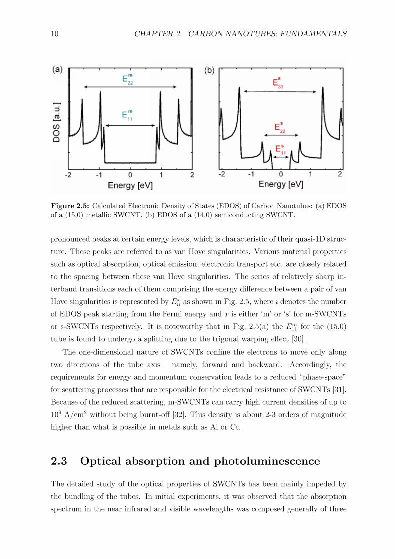
10 CHAPTER 2. CARBON NANOTUBES: FUNDAMENTALS
Figure 2.5: Calculated Electronic Density of States (EDOS) of Carbon Nanotubes: (a) EDOSof a (15,0) metallic SWCNT. (b) EDOS of a (14,0) semiconducting SWCNT.
pronounced peaks at certain energy levels, which is characteristic of their quasi-1D struc-
ture. These peaks are referred to as van Hove singularities. Various material properties
such as optical absorption, optical emission, electronic transport etc. are closely related
to the spacing between these van Hove singularities. The series of relatively sharp in-
terband transitions each of them comprising the energy difference between a pair of van
Hove singularities is represented by Exii as shown in Fig. 2.5, where i denotes the number
of EDOS peak starting from the Fermi energy and x is either ‘m’ or ‘s’ for m-SWCNTs
or s-SWCNTs respectively. It is noteworthy that in Fig. 2.5(a) the Em11 for the (15,0)
tube is found to undergo a splitting due to the trigonal warping effect [30].
The one-dimensional nature of SWCNTs confine the electrons to move only along
two directions of the tube axis – namely, forward and backward. Accordingly, the
requirements for energy and momentum conservation leads to a reduced “phase-space”
for scattering processes that are responsible for the electrical resistance of SWCNTs [31].
Because of the reduced scattering, m-SWCNTs can carry high current densities of up to
109 A/cm2 without being burnt-off [32]. This density is about 2-3 orders of magnitude
higher than what is possible in metals such as Al or Cu.
2.3 Optical absorption and photoluminescence
The detailed study of the optical properties of SWCNTs has been mainly impeded by
the bundling of the tubes. In initial experiments, it was observed that the absorption
spectrum in the near infrared and visible wavelengths was composed generally of three
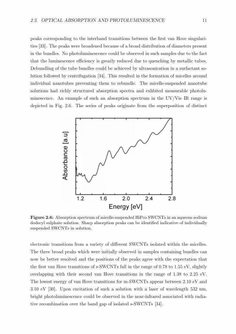
2.3. OPTICAL ABSORPTION AND PHOTOLUMINESCENCE 11
peaks corresponding to the interband transitions between the first van Hove singulari-
ties [33]. The peaks were broadened because of a broad distribution of diameters present
in the bundles. No photoluminescence could be observed in such samples due to the fact
that the luminescence efficiency is greatly reduced due to quenching by metallic tubes.
Debundling of the tube bundles could be achieved by ultrasonication in a surfactant so-
lution followed by centrifugation [34]. This resulted in the formation of micelles around
individual nanotubes preventing them to rebundle. The micelle-suspended nanotube
solutions had richly structured absorption spectra and exhbited measurable photolu-
minescence. An example of such an absorption spectrum in the UV/Vis–IR range is
depicted in Fig. 2.6. The series of peaks originate from the superposition of distinct
Figure 2.6: Absorption spectrum of micelle-suspended HiPco SWCNTs in an aqueous sodiumdodecyl sulphate solution. Sharp absorption peaks can be identified indicative of individuallysuspended SWCNTs in solution.
electronic transitions from a variety of different SWCNTs isolated within the micelles.
The three broad peaks which were initially observed in samples containing bundles can
now be better resolved and the positions of the peaks agree with the expectation that
the first van Hove transitions of s-SWCNTs fall in the range of 0.78 to 1.55 eV, slightly
overlapping with their second van Hove transitions in the range of 1.38 to 2.25 eV.
The lowest energy of van Hove transitions for m-SWCNTs appear between 2.10 eV and
3.10 eV [30]. Upon excitation of such a solution with a laser of wavelength 532 nm,
bright photoluminescence could be observed in the near-infrared associated with radia-
tive recombination over the band gap of isolated s-SWCNTs [34].
12 CHAPTER 2. CARBON NANOTUBES: FUNDAMENTALS
2.4 Phonon structure
2.4.1 Resonant Raman scattering
The main technique for probing the phonon spectra has been Raman spectroscopy.
Raman spectroscopy is a powerful tool that provides insight into the physical properties
as well as the material quality of an investigated system. A first order Raman scattering
process involves the absorption of an incoming photon with a certain frequency ωexc that
generates an electron-hole pair, which then scatters inelastically under the creation or
annihilation of a phonon (of frequency ωph). The scattered photon has a frequency ωsca
different from that of the incident photon. Energy and momentum are conserved in a
Raman process with ~ωexc = ~ωsca±~ωph. The ± signs refer to Stokes (phonon creation)
and anti-Stokes (phonon annihilation) scattering. In a typical Raman experiment, the
sample is irradiated with a laser source of a certain wavelength λexc and the scattered
light is recorded over a range of wavelengths very close to λexc. If λexc is such that the
incident photon energy is close to any transition energy, then resonant Raman scattering
occurs. In the case of SWCNTs, sharp van Hove maxima exist at certain energies. Thus
when they are excited by a laser wavelength with an energy close to their transition
energies, Raman scattering is remarkably enhanced [35].
The Kataura plot [36] can be used to illustrate the principle of resonant Raman
scattering in SWCNTs from the arc discharge and HiPco processes. The plot shows
the distribution of allowed transition energies Exii for SWCNTs in a range of diameters
as displayed in Fig. 2.7. For the purpose of excitation of the SWCNTs, laser radiation
in the visible region is utilized. The common wavelengths available with an Argon-
Krypton laser that were used in this work are the green (λexc = 514.5 nm) and red
(λexc = 647.1 nm) lines corresponding to energies of 2.41 eV and 1.92 eV respectively,
marked appropriately in the figure. The diameter range of the arc discharge and HiPco
SWCNTs are also marked as rectangles in the figure. It can be observed from the figure
that within the range of arc-discharge tubes (1.1–1.4 nm) a laser excitation using the
green line would excite exclusively the s-SWCNTs and the red line only the m-SWCNTs.
On the other hand, for samples fabricated using HiPco tubes, the red line would excite
only the s-SWCNTs and the green line the m-SWCNTs.
2.4.2 Phonon modes and Raman spectra
The phonon dispersion relations in SWCNTs can be obtained from those of the 2D
graphene sheet by using the same zone folding approach as used to derive the 1D elec-

2.4. PHONON STRUCTURE 13
Figure 2.7: Calculated energy separations Exii as a function of nanotube diameter between
0.7 and 3 nm(Kataura plot). The red circles refer to m-SWCNTs and the black ones to s-SWCNTs. The laser wavelengths used in this work are marked by the red and green linescorresponding to λexc = 647.1 nm and λexc = 514.5 nm respectively. The diameter range ofthe arc discharge SWCNTs is represented using a blue rectangle while that of HiPco SWCNTsusing a brown rectangle.
tronic dispersion relations [35]. The phonon dispersion relations for SWCNTs depend on
the indices (n, m), since the phonon wave vector in the circumferential direction becomes
discrete in accordance with the periodic boundary conditions of the chiral vector−→Ch. The
number of hexagons N in a unit cell of an (m, n) SWCNT is N = 2 (m2 + n2 + nm) /d.
Since there are 2N carbon atoms in the unit cell, each of them with three degrees of
freedom, the phonon dispersion relations consist of 6N branches. For example, a (10, 10)
SWCNT has 40 carbon atoms in the unit cell and correspondingly 120 vibrational de-
grees of freedom. But because of mode degeneracies there are only 66 distinct phonon
branches, of which 12 are non-degenerate and 54 are doubly degenerate.
Although the zone folding approach can compute the phonon branches of SWCNTs
that are similar to that of the graphene sheet, new modes occuring due to the curvature
of the nanotube are not predicted. For this, one has to introduce additional physical
concepts or use ab initio calculations. For example, the out-of-plane tangential acoustic
14 CHAPTER 2. CARBON NANOTUBES: FUNDAMENTALS
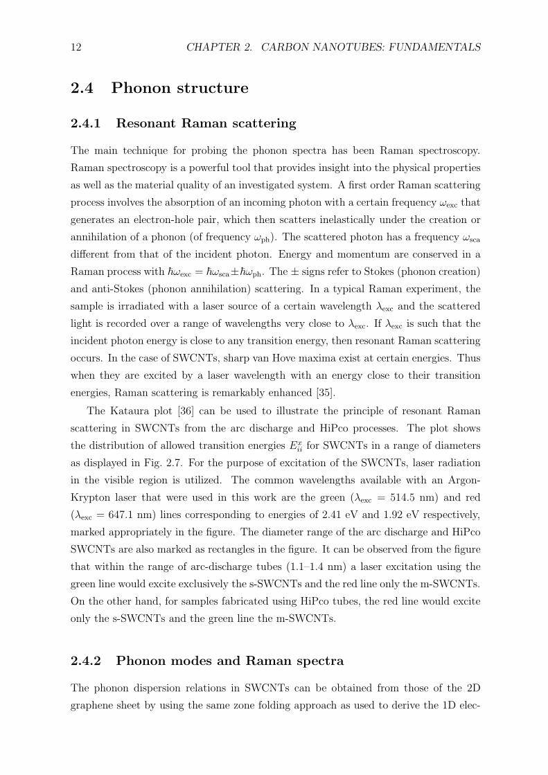
mode of a graphene sheet shown in Fig. 2.8(a) gives rise to the radial breathing mode
Figure 2.8: (a) The out-of-plane tangential mode in a graphene sheet gives rise to the radialbreathing mode (RBM) in a SWCNT. (b) The in-plane and out-of-plane modes do not couplein a graphene sheet while they indeed do upon rolling up of the sheet giving rise to a vibrationalmode perpendicular to the tube axis.
(RBM) in nanotubes and the resulting vibration does not have ω → 0 as k → 0.
Hence, the RBM is not an acoustic mode, but rather an optical mode with a non-zero
frequency at k = 0. In addition, in a graphene sheet, the in-plane and out-of-plane
modes are decoupled from each other. However, when the graphene sheet is rolled up
into a nanotube, the graphite-derived in-plane and out-of-plane modes do couple to each
other to form the acoustic mode of the nanotube as shown in Fig. 2.8(b).
The special symmetry properties of 1D SWCNTs results in only a few of the 6N
vibrational modes being Raman-active or infrared (IR)-active. Since only k vectors
very close to k = 0 are coupled to the incident light because of the energy-momentum
conservation requirements for the photons and phonons, only the modes close to the Γ
point are relevant. The numbers of Raman-active and IR-active modes can be obtained
by using group theory. Although group theory predicts the presence of 15 to 16 Raman-
active modes, only a few of them have sufficient cross-section to be detectable through
Raman spectroscopy. Among these, several modes close to 1600 cm−1 can be detected
that arise due to tangential vibrations of the carbon atoms. Since this set of modes
has its origin from the graphene sheet, they are referred to as the G-line in the Raman
spectrum. Another high frequency mode that can be detected by Raman spectroscopy is
the D-line occuring at about 1300 cm−1, which is related to the amount of defects within
2.5. CHEMICALLY FUNCTIONALIZED CARBON NANOTUBES 15
the nanotubes that lower the crystal symmetry of the sp2–bonded framework. The RBM
is also a Raman-active mode and occurs in the low frequency regime of around 100 to
300 cm−1. Apart from these a multitude of higher order modes can be identified in the
Raman spectra at frequencies higher than 1600 cm−1 arising due to a combination of
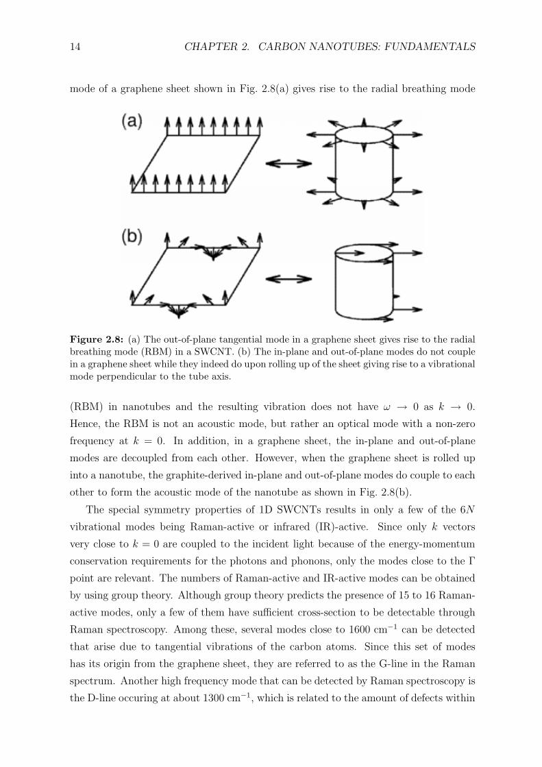
the RBM, D and G lines. A typical Raman spectrum from an individual bundle showing
the various lines is presented in Fig. 2.9. Two RBM peaks, the D-line and G-line can be
Figure 2.9: A typical Raman spectrum of a bundle of SWCNTs obtained with λexc =514.5 nm. Two RBM peaks can be identified at ≈ 129 cm−1 and 163 cm−1, in additionto the D-line at 1318 cm−1 and the G-line at 1566 cm−1. There are two higher modes ap-pearing in this tube bundle at 1717 cm−1 (attributed to RBM/G-line combination) and at2655 cm−1 (second order D-line).
easily identified in the spectrum. The D-line is very weak indicative of the bundle being
almost free of defects. Additionally, two higher order modes (marked by the asterisk
signs) can be recognized. The experimental setup for obtaining such a spectrum from
an individual SWCNT is detailed in the next chapter.
2.5 Chemically functionalized carbon nanotubes
On top of their excellent electrical and optical properties, nanotubes possess high me-
chanical and chemical stability. While the latter is certainly advantageous from an ap-
plication point of view, at the same time it imposes a severe hurdle for the development
of methods allowing for the selective and controlled functionalization of the nanotubes.
This explains why it was only within the past 3-4 years that a wider range of reliable
16 CHAPTER 2. CARBON NANOTUBES: FUNDAMENTALS
functionalization schemes became available. In this section, following a short discussion
of the chemical nature of SWCNTs, different functionalization schemes are summarized.
Specifically three different approaches have been undertaken for the chemical modifica-
tion of SWCNTs namely thermally activated chemistry, electrochemical modification
and photochemical functionalization.
2.5.1 Chemical nature of carbon nanotubes
Ideal SWCNTs possess two distinct regions of differing reactivity towards covalent chem-
ical modification. The presence of 5-membered rings at the caps leads to a relatively
higher reactivity there, which is comparable to that of fullerenes [37]. By comparison,
functionalization of the sidewall comprising the regular graphene framework is more dif-
ficult to accomplish. In general, addition reactions to the partial carbon-carbon double
bonds cause the transformation of sp2- into sp3-hybridized carbons, which is associated
with a change from a trigonal-planar to a tetrahedral local bonding geometry. This
process is energetically more favorable at the caps due to their pronounced curvature in
two dimensions, in marked contrast to the sidewall with its comparatively low curvature
in only one dimension. On the other hand, the non-zero curvature makes the sidewall
more reactive than the planar graphene sheet. Correspondingly, the binding energy of
atoms or functional groups on the sidewall should increase with decreasing tube diame-
ter. This tendency is supported by theoretical studies, as has been reported for instance
for the bonding of alkyl radicals to the SWCNT sidewall [38]. On the contrary, the
concave curvature of the inner surface of the nanotube imparts a very low reactivity
towards addition reactions [39], so that carbon nanotubes have been proposed as nano-
containers for reactive gas atoms, in analogy to fullerenes encapsulating nitrogen atoms
(e.g., N@C60).
In reality, however, nanotubes are no ideal structures, but rather contain defects
formed during synthesis. Typically around 1-3% of the carbon atoms of a nanotube
take part in a defect site [40]. A frequently encountered defect type is the so-called
Stone-Wales defect that comprises of two pairs of 5-membered and 7-membered rings,
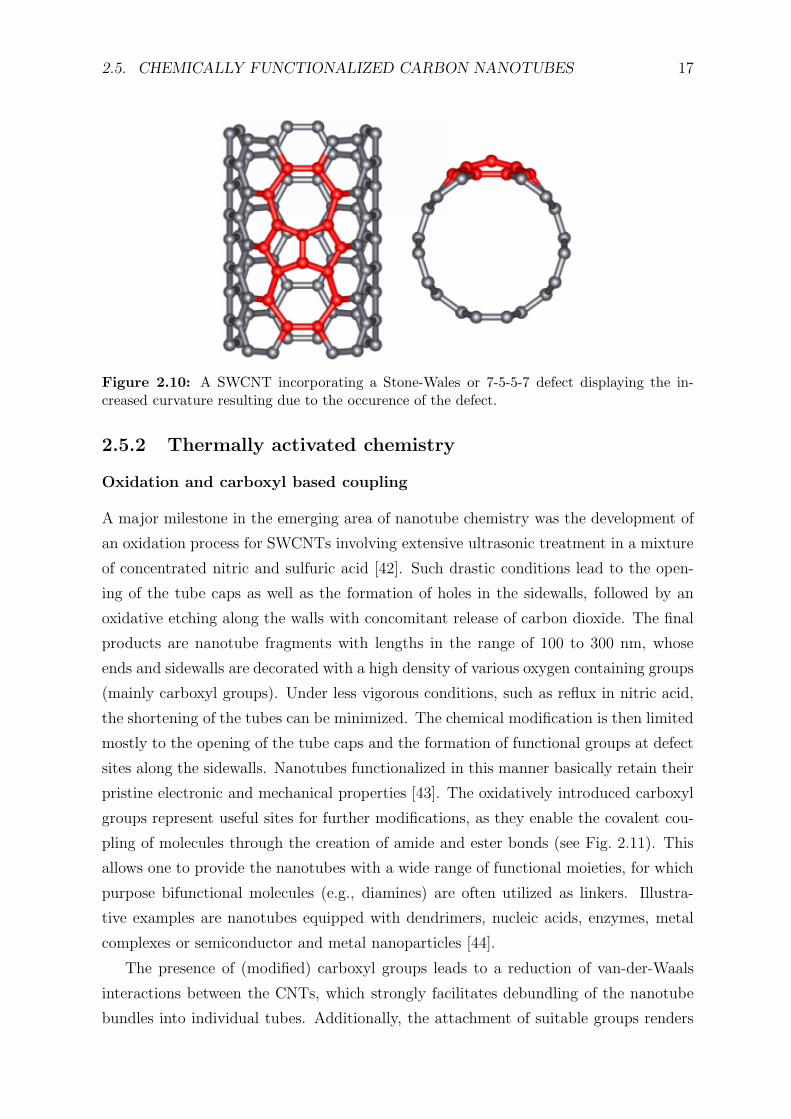
and is hence referred to as a 7-5-5-7 defect (see Fig. 2.10). A Stone-Wales defect leads
to a local deformation of the graphitic sidewall and thereby introduces an increased
curvature in this region. The strongest curvature exists at the interface between the two
five-membered rings, because of which an addition reaction is the most favored at the
C=C double bond there [41].
2.5. CHEMICALLY FUNCTIONALIZED CARBON NANOTUBES 17
Figure 2.10: A SWCNT incorporating a Stone-Wales or 7-5-5-7 defect displaying the in-creased curvature resulting due to the occurence of the defect.
2.5.2 Thermally activated chemistry
Oxidation and carboxyl based coupling
A major milestone in the emerging area of nanotube chemistry was the development of
an oxidation process for SWCNTs involving extensive ultrasonic treatment in a mixture
of concentrated nitric and sulfuric acid [42]. Such drastic conditions lead to the open-
ing of the tube caps as well as the formation of holes in the sidewalls, followed by an
oxidative etching along the walls with concomitant release of carbon dioxide. The final
products are nanotube fragments with lengths in the range of 100 to 300 nm, whose
ends and sidewalls are decorated with a high density of various oxygen containing groups
(mainly carboxyl groups). Under less vigorous conditions, such as reflux in nitric acid,
the shortening of the tubes can be minimized. The chemical modification is then limited
mostly to the opening of the tube caps and the formation of functional groups at defect
sites along the sidewalls. Nanotubes functionalized in this manner basically retain their
pristine electronic and mechanical properties [43]. The oxidatively introduced carboxyl
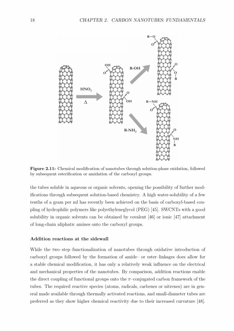
groups represent useful sites for further modifications, as they enable the covalent cou-
pling of molecules through the creation of amide and ester bonds (see Fig. 2.11). This
allows one to provide the nanotubes with a wide range of functional moieties, for which
purpose bifunctional molecules (e.g., diamines) are often utilized as linkers. Illustra-
tive examples are nanotubes equipped with dendrimers, nucleic acids, enzymes, metal
complexes or semiconductor and metal nanoparticles [44].
The presence of (modified) carboxyl groups leads to a reduction of van-der-Waals
interactions between the CNTs, which strongly facilitates debundling of the nanotube
bundles into individual tubes. Additionally, the attachment of suitable groups renders
18 CHAPTER 2. CARBON NANOTUBES: FUNDAMENTALS
Figure 2.11: Chemical modification of nanotubes through solution-phase oxidation, followedby subsequent esterification or amidation of the carboxyl groups.
the tubes soluble in aqueous or organic solvents, opening the possibility of further mod-
ifications through subsequent solution-based chemistry. A high water-solubility of a few
tenths of a gram per ml has recently been achieved on the basis of carboxyl-based cou-
pling of hydrophilic polymers like polyethyleneglycol (PEG) [45]. SWCNTs with a good
solubility in organic solvents can be obtained by covalent [46] or ionic [47] attachment
of long-chain aliphatic amines onto the carboxyl groups.
Addition reactions at the sidewall
While the two–step–functionalization of nanotubes through oxidative introduction of
carboxyl groups followed by the formation of amide– or ester–linkages does allow for
a stable chemical modification, it has only a relatively weak influence on the electrical
and mechanical properties of the nanotubes. By comparison, addition reactions enable
the direct coupling of functional groups onto the π–conjugated carbon framework of the
tubes. The required reactive species (atoms, radicals, carbenes or nitrenes) are in gen-
eral made available through thermally activated reactions, and small-diameter tubes are
preferred as they show higher chemical reactivity due to their increased curvature [48].
2.5. CHEMICALLY FUNCTIONALIZED CARBON NANOTUBES 19
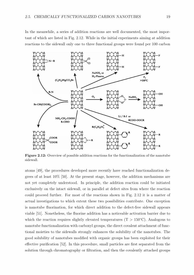
In the meanwhile, a series of addition reactions are well documented, the most impor-
tant of which are listed in Fig. 2.12. While in the initial experiments aiming at addition
reactions to the sidewall only one to three functional groups were found per 100 carbon
Figure 2.12: Overview of possible addition reactions for the functionalization of the nanotubesidewall.
atoms [49], the procedures developed more recently have reached functionalization de-
grees of at least 10% [50]. At the present stage, however, the addition mechanisms are
not yet completely understood. In principle, the addition reaction could be initiated
exclusively on the intact sidewall, or in parallel at defect sites from where the reaction
could proceed further. For most of the reactions shown in Fig. 2.12 it is a matter of
actual investigations to which extent these two possibilities contribute. One exception
is nanotube fluorination, for which direct addition to the defect-free sidewall appears
viable [51]. Nonetheless, the fluorine addition has a noticeable activation barrier due to
which the reaction requires slightly elevated temperatures (T > 150C). Analogous to
nanotube functionalization with carboxyl groups, the direct covalent attachment of func-
tional moieties to the sidewalls strongly enhances the solubility of the nanotubes. The
good solubility of nanotubes modified with organic groups has been exploited for their
effective purification [52]. In this procedure, small particles are first separated from the
solution through chromatography or filtration, and then the covalently attached groups
20 CHAPTER 2. CARBON NANOTUBES: FUNDAMENTALS
are removed through thermal annealing (T > 250C).
Substitution reactions on fluorinated nanotubes
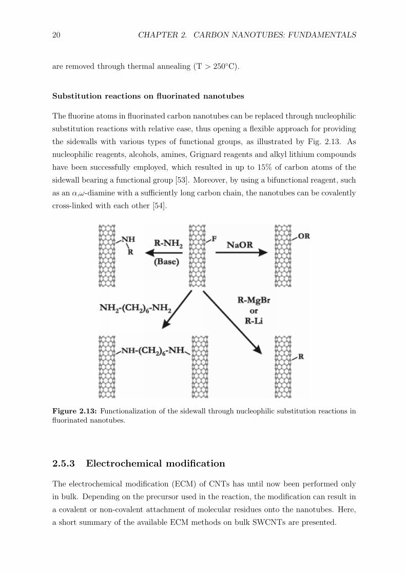
The fluorine atoms in fluorinated carbon nanotubes can be replaced through nucleophilic
substitution reactions with relative ease, thus opening a flexible approach for providing
the sidewalls with various types of functional groups, as illustrated by Fig. 2.13. As
nucleophilic reagents, alcohols, amines, Grignard reagents and alkyl lithium compounds
have been successfully employed, which resulted in up to 15% of carbon atoms of the
sidewall bearing a functional group [53]. Moreover, by using a bifunctional reagent, such
as an α,ω-diamine with a sufficiently long carbon chain, the nanotubes can be covalently
cross-linked with each other [54].
Figure 2.13: Functionalization of the sidewall through nucleophilic substitution reactions influorinated nanotubes.
2.5.3 Electrochemical modification
The electrochemical modification (ECM) of CNTs has until now been performed only
in bulk. Depending on the precursor used in the reaction, the modification can result in
a covalent or non-covalent attachment of molecular residues onto the nanotubes. Here,
a short summary of the available ECM methods on bulk SWCNTs are presented.
2.5. CHEMICALLY FUNCTIONALIZED CARBON NANOTUBES 21
Covalent ECM of SWCNTs in bulk
Covalent modification of SWCNTs has been successfully employed to attach organic
(aromatic) residues, as well as oxygen (oxidation) and halogen atoms (halogenation).
In these cases, the formation of covalent bonds has been concluded from changes in the
optical absorption or Raman spectra of the tubes. As the chemical reactivity of SWCNTs
increases with increasing curvature of their sidewalls [48], small diameter tubes have
often been used for covalent functionalization. Especially the HiPco SWCNT material
was frequently chosen, since it has a low minimum diameter of 0.7 nm. However, it
should be noted that the chemical reactivity of SWCNTs is not fully explored, and
there is some evidence obtained during the course of this work that also larger diameter
tubes (from the arc dicharge process) are sufficiently reactive, at least towards highly
active species [55].
Aromatic groups can be covalently linked to SWCNTs via reductive coupling of
diazonium salts. The diazonium-based attachment of (substituted) phenyl rings to SW-
CNT paper electrodes represents the first example of covalent ECM of SWCNTs [56].
Pronounced changes have been observed in the Raman spectra after modification,
specifically an increase in the relative intensity of the disorder mode peak (D-line) at
≈ 1290 cm−1, and a lowering of the intensity of RBM. While the former change di-
rectly indicates an increased amount of sp3-hybridized carbons, the latter signifies the
disturbance in the carbon framework of the sidewalls. Chemical analysis of the modified
products revealed that the extent of modification depends on the type of aryl diazonium
salt. Functionalization degrees of up to 0.05 have been found, which corresponds to one
in 20 carbon atoms bearing an aromatic residue. In the simplest scenario, the diazonium
salt is reduced by accepting an electron from the SWCNT, followed by loss of nitrogen
to form an aryl radical, and covalent binding of this radical to the intact sidewall via
addition to the partial double bonds. On the other hand, there are experimental in-
dications that the preferred attachment sites are defects [57]. Once started at such an
initiation site, the locally enhanced curvature would enhance the attachment of further
radicals, thus enabling the reaction to spread along the tube.
Noncovalent ECM of SWCNTs in bulk
The attachment of molecules onto the SWCNTs in a non-covalent manner is of in-
terest for some applications, since the carbon framework of the tubes remains intact,
and therefore their electronic properties are largely preserved. Non-covalent ECM has
been utilized to coat SWCNTs with a polymer consisting of polypyrrole or polyaniline,
22 CHAPTER 2. CARBON NANOTUBES: FUNDAMENTALS
which allows one to combine the specific properties of carbon nanotubes and electrically
conducting polymers (ECP) in a novel composite material [58]. High-resolution SEM
images revealed the presence of SWCNTs incorporated within the polypyrrole matrix,
and the formation of dense, high-quality composite films. It is possible to control the
thickness of the polymer coating on the tubes through the magnitude of the applied
potential and the duration of electropolymerization.
2.5.4 Photochemical functionalization
In contrast to the chemical functionalization routes based upon thermally activated
chemistry or electrochemistry, photochemical approaches have been employed to a much
lesser extent until now. Photo-irradiation has been used to generate reactive species such
as nitrenes in the course of sidewall addition reactions [59]. However, here the photo-
activation involves exclusively the azido compound employed as nitrene precursor. Only
one case of ”true” photochemical modification of SWCNTs has been reported to date,
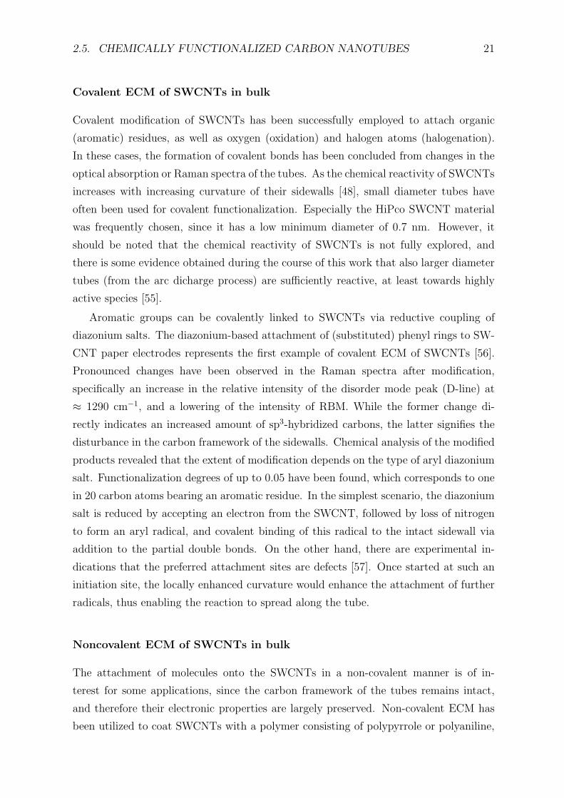
which is sidewall osmylation [60,61] Initially, it has been observed that SWCNTs exposed
to osmium tetroxide (OsO4) under UV-light irradiation show a pronounced increase in
electrical resistance (see Fig. 2.14). This change has been ascribed to the photo-induced
cycloaddition of OsO4 to the partial carbon/carbon double bonds, as a result of which
the π–electron density in the nanotubes is decreased. It is interesting to note that
when humidity is carefully avoided, the OsO4 addition is reversible, i.e. the cycloadduct
can be cleaved by photo-irradiation, whereby the original resistance is restored. In a
later stage, UV-light induced osmylation of SWCNTs has been studied also in organic
solvents [61]. Under these conditions, OsO4 appears to react preferentially with the
metallic tubes contained within the sample. This selectivity may originate from the
availability of electronic states at the Fermi level in the metallic tubes, which facilitates
the formation of an intermediate charge-transfer complex. As distinguished from the
reactions performed by exposure to gaseous OsO4, the major product in the organic
medium are SWCNTs decorated with OsO2 particles, resulting in the formation of
extended tube aggregates. This difference most likely arises from the fact that in the
latter case, the cycloadduct is readily hydrolyzed by the presence of water traces.
2.5. CHEMICALLY FUNCTIONALIZED CARBON NANOTUBES 23
Figure 2.14: (a) Reaction scheme for sidewall osmylation of a SWCNT using UV light. (b)Resistance change of an individiual m-SWCNT upon exposure to OsO4 and O2 under UV lightirradiation [60].

24 CHAPTER 2. CARBON NANOTUBES: FUNDAMENTALS
Chapter 3
Experimental
3.1 Sample preparation
For the experimental investigation of the nanotubes and for the fabrication of devices,
the SWCNTs have to be brought onto a substrate. There are two different methods to
perform this. The first method is based on the use of commercially available SWCNT
raw material obtained by arc-discharge. In the second method, the tubes are directly
grown on the substrate and are subsequently used for experiments. These two methods
are outlined in this section.
Arc discharge
The arc discharge method was first invented by Ebbesen and Ajayan [62] who achieved
growth and purification of MWCNTs at the gram level. This method, initially used
for producing fullerenes is the most common and easiest way to produce nanotubes.
However, the nanotubes obtained in this manner usually contain a large amount of
unwanted impurities. This method creates nanotubes through arc-vaporisation of two
carbon rods placed end to end in an inert atmosphere at low pressure. SWCNTs are
obtained in the presence of a metal catalyst [25,63]. In the current work, SWCNTs from
two different arc discharge processes have been used – Carbolex (Lexingtion, KY) [64]
and MER (Tucson, AZ) [65]. The diameter of the SWCNTs is in the range of 1.1 to
1.4 nm.
Procedures for the synthesis of large quantities of nanotubes invariably deliver bun-
dles (see for e.g. Fig. 3.1) that are composed of up to hundreds of single nanotubes
bound together by van der Waals interactions. It is advantageous, however to have indi-
vidually dispersed nanotubes instead of bundles for applications. This is important, for
25

26 CHAPTER 3. EXPERIMENTAL
example, in the fabrication of nano-scale devices where nanotubes of uniform properties
are a necessary prerequisite. Also while devising chemical functionalization schemes for
nanotubes, it is important to provide for easy access to chemical reagents. For this
purpose, ultrasonic treatment of the CNTs in an aqueous surfactant solution has turned
out to be effective [34], which leads to the enclosure of the individual tubes in a deter-
gent shell. It should be stressed that the experimental conditions have to be carefully
controlled, since intensive ultrasonication may otherwise cause noticeable damage of the
tube walls [66].
Figure 3.1: A low temperature scanning tunneling microscope (STM) image showing anatomically resolved SWCNT bundle composed of at least 8 individual tubes. (Courtesy:Dr. Lucia Vitali)
A 1 wt.% aqueous solution of sodium dodecylsulphate (SDS) or lithium dodecyl-
sulphate (LDS) is used to disperse the SWCNTs using an ultrasonic stick mixer. This
solution is then left in an ultrasonic bath for a few minutes to enable further debundling.
Upon centrifuging this dispersion, the heavy catalyst particles and big bundles are sed-
imented out at the bottom. The supernatant of the resulting suspension is placed on
a substrate, after the surface is treated for 2 m in an aqueous solution of 0.1 vol.% 3–
(aminopropyl)triethoxysilane. After an adsorption time of 30 m, the substrate surface
is dried in a stream of nitrogen and then rinsed in ultra-pure water and dried again.
This procedure yields a random distribution of the nanotubes on the surface. Based on
the specific application for which the samples are produced and depending on the raw
material used, the parameters of ultrasonication, the speed of centrifuge and the time of
deposition need to be carefully controlled. For example, a high fraction of single tubes
are obtained with a strong ultrasonication and a short deposition time, while dense
3.1. SAMPLE PREPARATION 27
networks require a rather weaker ultrasonication with a longer deposition time.
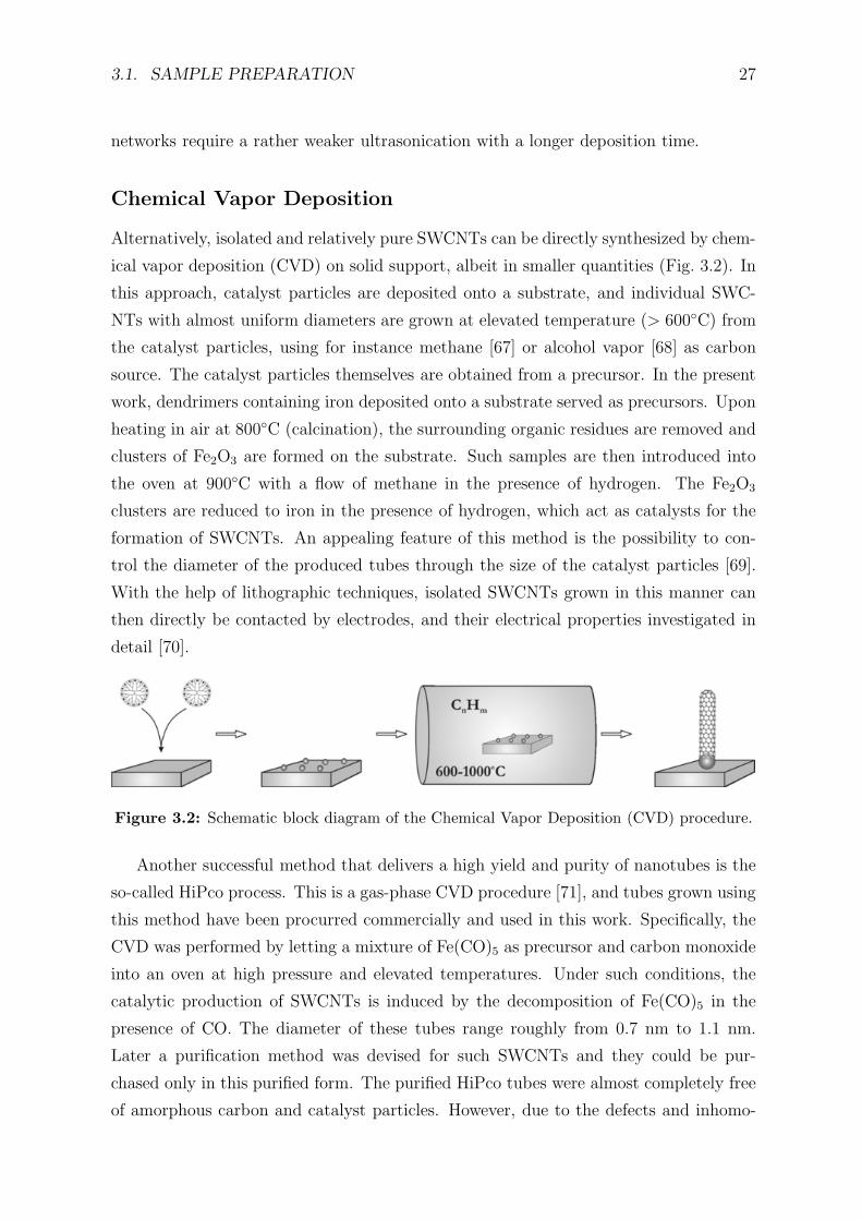
Chemical Vapor Deposition
Alternatively, isolated and relatively pure SWCNTs can be directly synthesized by chem-
ical vapor deposition (CVD) on solid support, albeit in smaller quantities (Fig. 3.2). In
this approach, catalyst particles are deposited onto a substrate, and individual SWC-
NTs with almost uniform diameters are grown at elevated temperature (> 600C) from
the catalyst particles, using for instance methane [67] or alcohol vapor [68] as carbon
source. The catalyst particles themselves are obtained from a precursor. In the present
work, dendrimers containing iron deposited onto a substrate served as precursors. Upon
heating in air at 800C (calcination), the surrounding organic residues are removed and
clusters of Fe2O3 are formed on the substrate. Such samples are then introduced into
the oven at 900C with a flow of methane in the presence of hydrogen. The Fe2O3
clusters are reduced to iron in the presence of hydrogen, which act as catalysts for the
formation of SWCNTs. An appealing feature of this method is the possibility to con-
trol the diameter of the produced tubes through the size of the catalyst particles [69].
With the help of lithographic techniques, isolated SWCNTs grown in this manner can
then directly be contacted by electrodes, and their electrical properties investigated in
detail [70].
Figure 3.2: Schematic block diagram of the Chemical Vapor Deposition (CVD) procedure.
Another successful method that delivers a high yield and purity of nanotubes is the
so-called HiPco process. This is a gas-phase CVD procedure [71], and tubes grown using
this method have been procurred commercially and used in this work. Specifically, the
CVD was performed by letting a mixture of Fe(CO)5 as precursor and carbon monoxide
into an oven at high pressure and elevated temperatures. Under such conditions, the
catalytic production of SWCNTs is induced by the decomposition of Fe(CO)5 in the
presence of CO. The diameter of these tubes range roughly from 0.7 nm to 1.1 nm.
Later a purification method was devised for such SWCNTs and they could be pur-
chased only in this purified form. The purified HiPco tubes were almost completely free
of amorphous carbon and catalyst particles. However, due to the defects and inhomo-
28 CHAPTER 3. EXPERIMENTAL
geneities introduced during the purification procedure, their electrical performance was
quite poor as observed in our electronic transport investigations on such tubes.
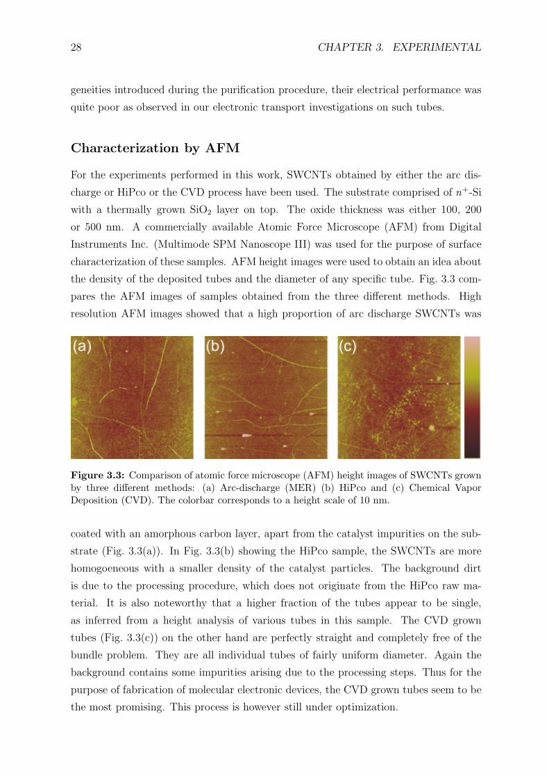
Characterization by AFM
For the experiments performed in this work, SWCNTs obtained by either the arc dis-
charge or HiPco or the CVD process have been used. The substrate comprised of n+-Si
with a thermally grown SiO2 layer on top. The oxide thickness was either 100, 200
or 500 nm. A commercially available Atomic Force Microscope (AFM) from Digital
Instruments Inc. (Multimode SPM Nanoscope III) was used for the purpose of surface
characterization of these samples. AFM height images were used to obtain an idea about
the density of the deposited tubes and the diameter of any specific tube. Fig. 3.3 com-
pares the AFM images of samples obtained from the three different methods. High
resolution AFM images showed that a high proportion of arc discharge SWCNTs was
Figure 3.3: Comparison of atomic force microscope (AFM) height images of SWCNTs grownby three different methods: (a) Arc-discharge (MER) (b) HiPco and (c) Chemical VaporDeposition (CVD). The colorbar corresponds to a height scale of 10 nm.
coated with an amorphous carbon layer, apart from the catalyst impurities on the sub-
strate (Fig. 3.3(a)). In Fig. 3.3(b) showing the HiPco sample, the SWCNTs are more
homogoeneous with a smaller density of the catalyst particles. The background dirt
is due to the processing procedure, which does not originate from the HiPco raw ma-
terial. It is also noteworthy that a higher fraction of the tubes appear to be single,
as inferred from a height analysis of various tubes in this sample. The CVD grown
tubes (Fig. 3.3(c)) on the other hand are perfectly straight and completely free of the
bundle problem. They are all individual tubes of fairly uniform diameter. Again the
background contains some impurities arising due to the processing steps. Thus for the
purpose of fabrication of molecular electronic devices, the CVD grown tubes seem to be
the most promising. This process is however still under optimization.
3.2. ELECTRONIC TRANSPORT MEASUREMENTS 29
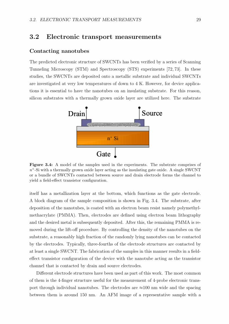
3.2 Electronic transport measurements
Contacting nanotubes
The predicted electronic structure of SWCNTs has been verified by a series of Scanning
Tunneling Microscopy (STM) and Spectroscopy (STS) experiments [72, 73]. In these
studies, the SWCNTs are deposited onto a metallic substrate and individual SWCNTs
are investigated at very low temperatures of down to 4 K. However, for device applica-
tions it is essential to have the nanotubes on an insulating substrate. For this reason,
silicon substrates with a thermally grown oxide layer are utilized here. The substrate
Figure 3.4: A model of the samples used in the experiments. The substrate comprises ofn+-Si with a thermally grown oxide layer acting as the insulating gate oxide. A single SWCNTor a bundle of SWCNTs contacted between source and drain electrode forms the channel toyield a field-effect transistor configuration.
itself has a metallization layer at the bottom, which functions as the gate electrode.
A block diagram of the sample composition is shown in Fig. 3.4. The substrate, after
deposition of the nanotubes, is coated with an electron beam resist namely polymethyl-
methacrylate (PMMA). Then, electrodes are defined using electron beam lithography
and the desired metal is subsequently deposited. After this, the remaining PMMA is re-
moved during the lift-off procedure. By controlling the density of the nanotubes on the
substrate, a reasonably high fraction of the randomly lying nanotubes can be contacted
by the electrodes. Typically, three-fourths of the electrode structures are contacted by
at least a single SWCNT. The fabrication of the samples in this manner results in a field-
effect transistor configuration of the device with the nanotube acting as the transistor
channel that is contacted by drain and source electrodes.
Different electrode structures have been used as part of this work. The most common
of them is the 4-finger structure useful for the measurement of 4-probe electronic trans-
port through individual nanotubes. The electrodes are ≈100 nm wide and the spacing
between them is around 150 nm. An AFM image of a representative sample with a
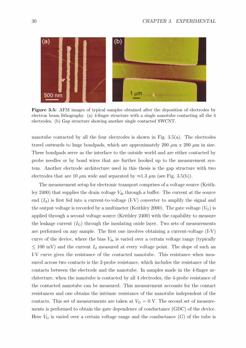
30 CHAPTER 3. EXPERIMENTAL
Figure 3.5: AFM images of typical samples obtained after the deposition of electrodes byelectron beam lithography. (a) 4-finger structure with a single nanotube contacting all the 4electrodes. (b) Gap structure showing another single contacted SWCNT.
nanotube contacted by all the four electrodes is shown in Fig. 3.5(a). The electrodes
travel outwards to huge bondpads, which are approximately 200 µm x 200 µm in size.
These bondpads serve as the interface to the outside world and are either contacted by
probe needles or by bond wires that are further hooked up to the measurement sys-
tem. Another electrode architecture used in this thesis is the gap structure with two
electrodes that are 10 µm wide and separated by ≈1.3 µm (see Fig. 3.5(b)).
The measurement setup for electronic transport comprises of a voltage source (Keith-
ley 2400) that supplies the drain voltage Vds through a buffer. The current at the source
end (Id) is first fed into a current-to-voltage (I-V) converter to amplify the signal and
the output voltage is recorded by a multimeter (Keithley 2000). The gate voltage (VG) is
applied through a second voltage source (Keithley 2400) with the capability to measure
the leakage current (IG) through the insulating oxide layer. Two sets of measurements
are performed on any sample. The first one involves obtaining a current-voltage (I-V)
curve of the device, where the bias Vds is varied over a certain voltage range (typically
≤ 100 mV) and the current Id measured at every voltage point. The slope of such an
I-V curve gives the resistance of the contacted nanotube. This resistance when mea-
sured across two contacts is the 2-probe resistance, which includes the resistance of the
contacts between the electrode and the nanotube. In samples made in the 4-finger ar-
chitecture, when the nanotube is contacted by all 4 electrodes, the 4-probe resistance of
the contacted nanotube can be measured. This measurement accounts for the contact
resistances and one obtains the intrinsic resistance of the nanotube independent of the
contacts. This set of measurements are taken at VG = 0 V. The second set of measure-
ments is performed to obtain the gate dependence of conductance (GDC) of the device.
Here VG is varied over a certain voltage range and the conductance (G) of the tube is
3.2. ELECTRONIC TRANSPORT MEASUREMENTS 31
measured at every value of VG at small drain-source bias, providing information about
the switching capability of the device.
Room-temperature measurements
Room-temperature electronic transport measurements are used to find out if a specific
contacted nanotube is metallic or semiconducting. Following the fabrication of the
device, AFM images are used to determine if a certain electrode structure incorporates
a contacted SWCNT. The diameter of the SWCNT can be obtained from the AFM
height images. Subsequently the resistance and the GDC of the device are measured
at room temperature. With the same electrode material and the same type of SWCNT
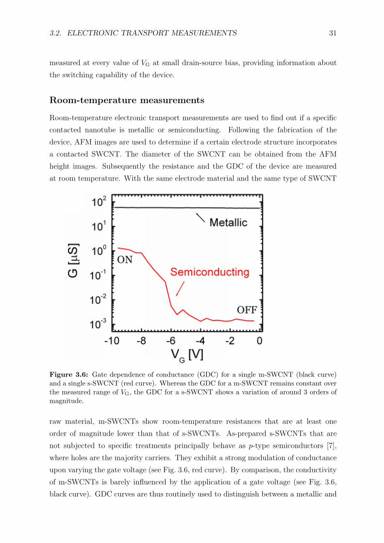
Figure 3.6: Gate dependence of conductance (GDC) for a single m-SWCNT (black curve)and a single s-SWCNT (red curve). Whereas the GDC for a m-SWCNT remains constant overthe measured range of VG, the GDC for a s-SWCNT shows a variation of around 3 orders ofmagnitude.
raw material, m-SWCNTs show room-temperature resistances that are at least one
order of magnitude lower than that of s-SWCNTs. As-prepared s-SWCNTs that are
not subjected to specific treatments principally behave as p-type semiconductors [7],
where holes are the majority carriers. They exhibit a strong modulation of conductance
upon varying the gate voltage (see Fig. 3.6, red curve). By comparison, the conductivity
of m-SWCNTs is barely influenced by the application of a gate voltage (see Fig. 3.6,
black curve). GDC curves are thus routinely used to distinguish between a metallic and
32 CHAPTER 3. EXPERIMENTAL
a semiconducting nanotube. The high conductance state is referred to as the ON state
and the low conductance the OFF state. For the purpose of quantifying the switching
ability, it is worthwhile introducing a unitless quantity called the Gate Dependence
Ratio (GDR), which is the ratio of the ON conductance to the OFF conductance.
Purely m-SWCNTs have a GDR between 1 and 2, while s-SWCNTs show a GDR of at
least 103.
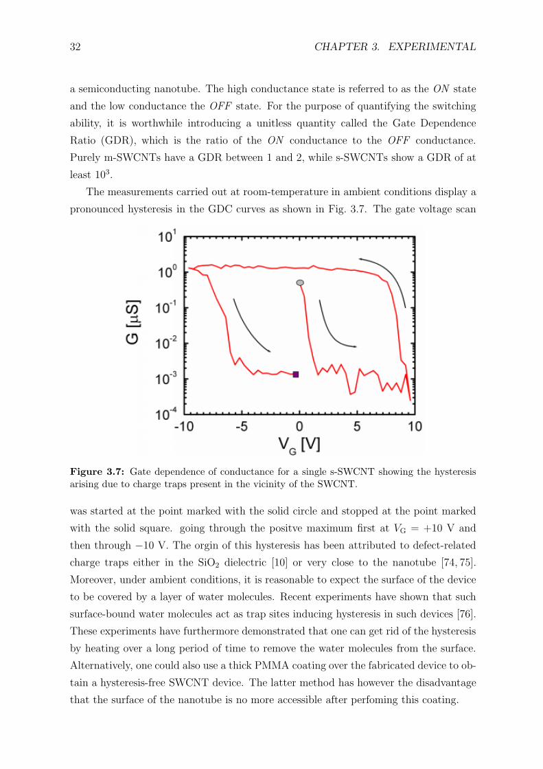
The measurements carried out at room-temperature in ambient conditions display a
pronounced hysteresis in the GDC curves as shown in Fig. 3.7. The gate voltage scan
Figure 3.7: Gate dependence of conductance for a single s-SWCNT showing the hysteresisarising due to charge traps present in the vicinity of the SWCNT.
was started at the point marked with the solid circle and stopped at the point marked
with the solid square. going through the positve maximum first at VG = +10 V and
then through −10 V. The orgin of this hysteresis has been attributed to defect-related
charge traps either in the SiO2 dielectric [10] or very close to the nanotube [74, 75].
Moreover, under ambient conditions, it is reasonable to expect the surface of the device
to be covered by a layer of water molecules. Recent experiments have shown that such
surface-bound water molecules act as trap sites inducing hysteresis in such devices [76].
These experiments have furthermore demonstrated that one can get rid of the hysteresis
by heating over a long period of time to remove the water molecules from the surface.
Alternatively, one could also use a thick PMMA coating over the fabricated device to ob-
tain a hysteresis-free SWCNT device. The latter method has however the disadvantage
that the surface of the nanotube is no more accessible after perfoming this coating.
3.2. ELECTRONIC TRANSPORT MEASUREMENTS 33
Metallic SWCNTs
The coherence length of electrons travelling in carbon nanotubes is of the order of
500 nm [77]. Thus in short nanotube fragments, electrons can travel from one end
to the other without any appreciable scattering. In such cases where the transport
is ballistic, the conductance of a nanotube is given by Landauer’s equation [78] as
G = (2e2/h)∑N
i Ti, where 2e2/h is the conductance quantum and Ti is the transmission
probability of each subband (conduction channel) that is contributing to transport.
As shown earlier, there are two subbands crossing at the Fermi energy for a metallic
nanotube and hence N = 2. In the absence of scattering (Ti = 1, ballistic transport),
the conductance of a m-SWCNT at low electron energies is 4e2/h. Alternatively, the
two-terminal resistance of a m-SWCNT in the ideal case is ≈ 6.5 kΩ. This resistance
is a contact resistance arising due to the mismatch between the number of conduction
channels in the SWCNT and the macroscopic metal leads [79]. In addition to this
mismatch, poor coupling between the leads and the SWCNT can increase the two-
terminal resistance of a m-SWCNT.
The type of the metal used to contact the SWCNTs determines the coupling be-
tween the leads and the SWCNT. Ohmic contacts with minimum contact resistance are
important to achieve the best coupling. Such ohmic contacts to individual m-SWCNTs
have been possible by Cr [80] and pure Pd [77]. This has enabled the observation of
quasi-ballistic transport at low-temperatures, with conductances of the order of 3e2/h
at 4 K. Although ballistic transport has been observed with Ti (G4K ≈ 2e2/h) [81], such
contacts are less reliable and their reproducibility has been found to be quite poor [82].
In these experiments, the low-temperature conductance was greater than 2e2/h imply-
ing that at least one transport channel was intact and the coupling was near optimal.
Upon cooling from room-temperature, the resistance of such samples decreased due to
the suppression of phonon-scattering at lower temperatures [83]. On the other hand,
individual defect-free m-SWCNTs contacted by other metals show in general G < 2e2/
h at room-temperature. The resistance of such samples increases upon lowering the
temperature [84, 85], signifying that potential barriers at the contacts formed due to
sub-optimal coupling have a strong impact on the transport.
In this work mainly two types of contacts have been used. In the first category
of samples, a Ti adhesion layer (typically less than 1 nm) was evaporated onto the
SWCNTs followed by 15 nm of AuPd. The second set of samples was fabricated with
AuPd electrodes directly contacting the SWCNTs. In both of these types of samples
the room-temperature conductances were much lower than 2e2/h. The conductance de-
creased upon lowering the temperature indicating that the transport in these samples
34 CHAPTER 3. EXPERIMENTAL
was strongly restricted by the barriers at the contacts. The reduction in conductance
upon cooling could also be explained by the presence of structural defects such as vacan-
cies, pentagon-heptagon pairs and Stone-Wales defects [31]. However, in such a case a
weak gate dependence of conductance would be observed [86]. The GDC curves of such
defective tubes exhibit gate dependence ratios in the range of 3 to 100. Thus the GDC
curves, apart from being able to distinguish between m-SWCNTs and s-SWCNTs, can
also be effectively used to identify if a contacted tube is defect-free or not.
Semiconducting SWCNTs
Similar to the case of m-SWCNTs, the electrical characteristics of s-SWCNTs is depen-
dent to a large extent on the type of metal used to contact them. s-SWCNTs contacted
by gold electrodes in general exhibit a p-type behavior due to the Fermi level of gold
aligning with the valence band of the s-SWCNT, making a barrier for the injection of
electrons [87]. It was found that this p-type behaviour in s-SWCNT-FETs is due to
the formation of Schottky barriers at the contacts, rather than an intrinsic effect [88].
Later experiments [89] confirmed that the electrical performance of such FET devices
was restricted by the existence of these Schottky barriers and their response to the ap-
plied electric fields. Thermionic emission and tunneling are involved in transport across
the barriers, which limit the ON state conductance of a nanotube FET to well below
the 4e2/h limit at room temperature [88, 90]. The use of Ti as the contacting metal
followed by a rapid thermal annealing procedure helped in the achievement of ambipo-
lar transport in SWCNTs [91] exhibiting relatively low resistance for the injection of
both p-type and n-type carriers. However, ballistic transport could still not be observed
in the Ti-contacted SWCNT FETs. Only recently, it has been shown that contacting
short segment s-SWCNTs (of length < 500 nm) by Pd greatly reduces or eliminates the
barriers for transport yielding ballistic s-SWCNT-FETs [11]. In the samples used in this
work, s-SWCNTs contacted by AuPd/Ti electrodes have been found to exhibit lower
ON conductances than those contacted by AuPd, signifying that the Schottky barriers
in the former case is higher and/or wider than that in the latter.
3.3 Confocal laser scanning microscopy
Initial experiments on Raman spectroscopy of carbon nanotubes used focussed laser
beams of µm spot sizes and generally probed a sample containing a large amount of
SWCNTs in solution. A spectrograph was used to collect the scattered light from the
whole solution. Due to the presence of a large number of tubes in such samples, a
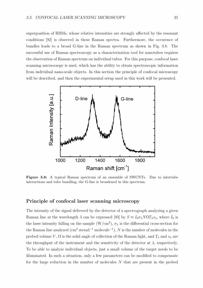
3.3. CONFOCAL LASER SCANNING MICROSCOPY 35
superposition of RBMs, whose relative intensities are strongly affected by the resonant
conditions [92] is observed in these Raman spectra. Furthermore, the occurence of
bundles leads to a broad G-line in the Raman spectrum as shown in Fig. 3.8. The
successful use of Raman spectroscopy as a characterization tool for nanotubes requires
the observation of Raman spectrum on individual tubes. For this purpose, confocal laser
scanning micrsocsopy is used, which has the ability to obtain spectroscopic information
from individual nano-scale objects. In this section the principle of confocal microscopy
will be described, and then the experimental setup used in this work will be presented.
Figure 3.8: A typical Raman spectrum of an ensemble of SWCNTs. Due to intertubeinteractions and tube bundling, the G-line is broadened in this spectrum.
Principle of confocal laser scanning microscopy
The intensity of the signal delivered by the detector of a spectrograph analyzing a given
Raman line at the wavelength λ can be expressed [93] by S ≈ I0σλNΩTλsλ, where I0 is
the laser intensity falling on the sample (W/cm2), σλ is the differential cross-section for
the Raman line analyzed (cm2 sterad−1 molecule−1), N is the number of molecules in the
probed volume V , Ω is the solid angle of collection of the Raman light, and Tλ and sλ are
the throughput of the instrument and the sensitivity of the detector at λ, respectively.
To be able to analyze individual objects, just a small volume of the target needs to be
illuminated. In such a situation, only a few parameters can be modified to compensate
for the large reduction in the number of molecules N that are present in the probed
36 CHAPTER 3. EXPERIMENTAL
volume V . These are the incident light intensity I0 and the solid angle of collection
Ω. It was found that the use of the same microscope objective for both illuminating
the sample and collecting the scattered light (and hence the name confocal microscopy)
was the best way to decrease V while simultaneously increasing Ω and I0. Indeed, high
magnification microscope objectives, which have high-numerical aperture (NA) optics
are able to focus the laser beam into a very small volume and to collect, under a wide
angle, the light scattered by this volume. Thus both the enormous increase of the local
laser intensity I0 and the wide angle of collection Ω compensate for the decrease of the
number of molecules N . The smallest size of the illumination spot that can be achieved
in this manner is diffraction-limited, and the diameter of such a spot that is obtainable
with a very good objective is ≈ λexc/2.
Confocal microscopy thus enables the maximum possible resolution in the optical far-
field through a combination of optical excitation onto and detection from a diffraction-
limited volume of the sample. The microscope is based on the use of a highly focussed
laser beam for illuminating the sample combined with the use of a pin-hole as a spatial
filter for detection. The pin-hole ensures that only scattered light from the illuminated
volume passes through to the detector and thus delivers a huge enhancement in resolu-
tion along the axial direction. Since this light contains no spatial information, a point
detector is sufficient to analyze the scattered light. To be able to still obtain an image
of the sample, the excitation volume in connection with the detection volume must be
continuously shifted with respect to the sample. This can be done in two different ways.
In the first method that has been implemented in the confocal microscope used in this
work, the sample is raster-scanned below the stationary focal spot of the microscope.
The second method utilizes a scanning laser beam with a stationary sample to obtain
an image of the sample. In contrast to the usual far-field imaging using a conventional
microscope where the imaging is done at once, confocal imaging is a sequential proce-
dure. It is possible to obtain images in various planes of a thick sample and obtain a
3D reconstruction of the analyzed data. The scattered light that is collected by the
microscope constitutes the Rayleigh, fluorescence and Raman components. Through
appropriate optical instrumentation the desired component can be filtered and recorded
as a function of position of the sample. This results in confocal reflection, confocal
fluorescence or confocal Raman images, respectively.
Instrumentation
The experimental setup of the confocal laser microscope used in this work [94] is de-
picted in Fig. 3.9. It comprises of an Argon-Krypton ion laser (Coherent, Innova 70
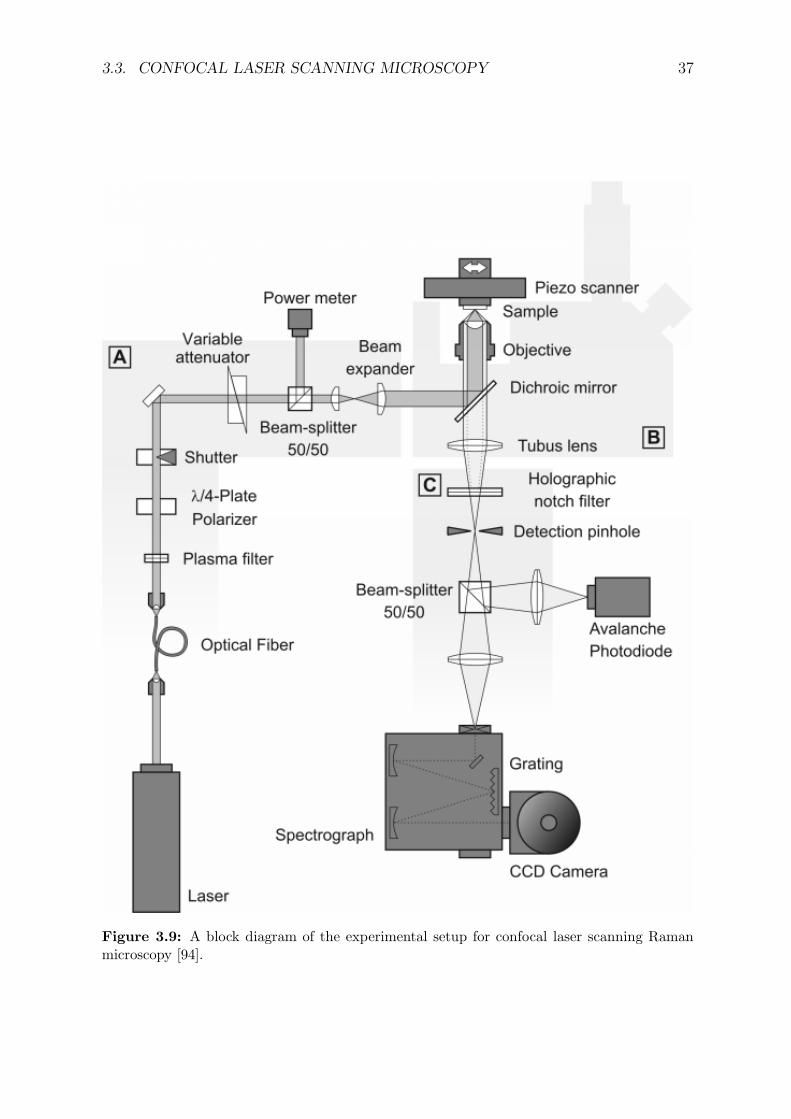
3.3. CONFOCAL LASER SCANNING MICROSCOPY 37
Figure 3.9: A block diagram of the experimental setup for confocal laser scanning Ramanmicroscopy [94].
38 CHAPTER 3. EXPERIMENTAL
Spectrum) that is used as the source of linearly polarized monochromatic light with
wavelengths of 647.1 nm and 514.5 nm. To avoid the spatial drift of the laser beam
(lateral displacement during adjustment and thermal drift of the laser resonator), the
laser light is first passed through a monomode glass fiber and then through a plasma
filter, which allows light of just the desired wavelength to pass through. This is fol-
lowed immediately by a polarizer and a λ/4-plate that produces circularly polarized
light. This is important to ensure that SWCNTs of various orientations lying on the
substrate can all be uniformly excited, since the efficiency of excitation is dependent on
the relative orientation of the nanotube axis with respect to the light polarization. For
performing polarization-dependent measurements, a motorized polarizer was addition-
ally introduced, which enabled to continuously modulate the polarization of the incident
light beam with a specified frequency. The beam is then guided through various mirrors
into a variable attenuator with the help of which the intensity of the laser beam could
be varied between 0.3 mW and 15 mW. Before entering the microscope (Zeiss Axiovert
135 TV), the beam is conditioned through a system of lenses to enable maximum illu-
mination of the microscope objective. The objective then focusses the beam down to a
spot that is diffraction-limited in size. For performing the Raman experiments, a 100X
objective (f = 1.645 mm) with an NA of 0.9 and a working distance of 0.27 mm was
used. The lateral resolution that is achievable mainly depends on the NA of the objec-
tives, and is given by 0.4λexc/NA. Usually a power of 1 mW is used in the experiments
that corresponds to a light intensity of ≈0.5 MW/cm2 at the center of the focussed
diffraction-limited spot. As discussed earlier, this value of I0 is quite high, which helps
in compensating for the reduction in the volume V of the sample that is illuminated.
The SWCNTs can withstand such high light intensities for a reasonable period of time
(in the order of a few hours). But upon prolonged exposure for more than 6 hours,
defects were found to be introduced in the nanotubes.
The scattered light from the sample collected by the same objective lens passes
through a 50:50 semi-transparent mirror and is then focussed onto a pinhole through a
convex lens. This detection pinhole is responsible for filtering the stray light arising from
sources that are out of the illumination volume, and hence to improve the signal-to-noise
ratio. The filtered beam contains a strong Rayleigh component due to the high inten-
sity of the incident laser beam. To suppress this component, a holographic notch filter
(Super-Notch-Plus) centered at the laser wavelength is used. This filter attenuates the
incoming signal strongly in a small band of ±100 cm−1 around the specified wavelength.
The Raman components in the scattered light are normally around 30 orders of mag-
nitude weaker than the Rayleigh component. Thus the attenuated light still contains a
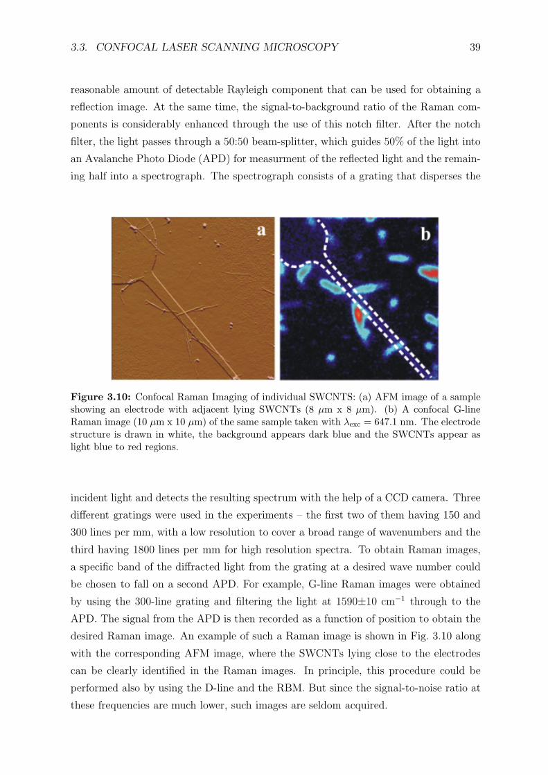
3.3. CONFOCAL LASER SCANNING MICROSCOPY 39
reasonable amount of detectable Rayleigh component that can be used for obtaining a
reflection image. At the same time, the signal-to-background ratio of the Raman com-
ponents is considerably enhanced through the use of this notch filter. After the notch
filter, the light passes through a 50:50 beam-splitter, which guides 50% of the light into
an Avalanche Photo Diode (APD) for measurment of the reflected light and the remain-
ing half into a spectrograph. The spectrograph consists of a grating that disperses the
Figure 3.10: Confocal Raman Imaging of individual SWCNTS: (a) AFM image of a sampleshowing an electrode with adjacent lying SWCNTs (8 µm x 8 µm). (b) A confocal G-lineRaman image (10 µm x 10 µm) of the same sample taken with λexc = 647.1 nm. The electrodestructure is drawn in white, the background appears dark blue and the SWCNTs appear aslight blue to red regions.
incident light and detects the resulting spectrum with the help of a CCD camera. Three
different gratings were used in the experiments – the first two of them having 150 and
300 lines per mm, with a low resolution to cover a broad range of wavenumbers and the
third having 1800 lines per mm for high resolution spectra. To obtain Raman images,
a specific band of the diffracted light from the grating at a desired wave number could
be chosen to fall on a second APD. For example, G-line Raman images were obtained
by using the 300-line grating and filtering the light at 1590±10 cm−1 through to the
APD. The signal from the APD is then recorded as a function of position to obtain the
desired Raman image. An example of such a Raman image is shown in Fig. 3.10 along
with the corresponding AFM image, where the SWCNTs lying close to the electrodes
can be clearly identified in the Raman images. In principle, this procedure could be
performed also by using the D-line and the RBM. But since the signal-to-noise ratio at
these frequencies are much lower, such images are seldom acquired.
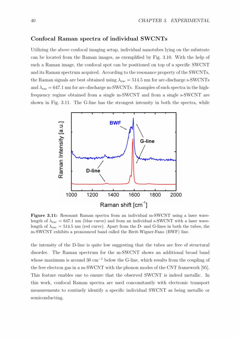
40 CHAPTER 3. EXPERIMENTAL
Confocal Raman spectra of individual SWCNTs
Utilizing the above confocal imaging setup, individual nanotubes lying on the substrate
can be located from the Raman images, as exemplified by Fig. 3.10. With the help of
such a Raman image, the confocal spot can be positioned on top of a specific SWCNT
and its Raman spectrum acquired. According to the resonance property of the SWCNTs,
the Raman signals are best obtained using λexc = 514.5 nm for arc-discharge s-SWCNTs
and λexc = 647.1 nm for arc-discharge m-SWCNTs. Examples of such spectra in the high-
frequency regime obtained from a single m-SWCNT and from a single s-SWCNT are
shown in Fig. 3.11. The G-line has the strongest intensity in both the spectra, while
Figure 3.11: Resonant Raman spectra from an individual m-SWCNT using a laser wave-length of λexc = 647.1 nm (blue curve) and from an individual s-SWCNT with a laser wave-length of λexc = 514.5 nm (red curve). Apart from the D- and G-lines in both the tubes, them-SWCNT exhibits a pronounced band called the Breit-Wigner-Fano (BWF) line.
the intensity of the D-line is quite low suggesting that the tubes are free of structural
disorder. The Raman spectrum for the m-SWCNT shows an additional broad band
whose maximum is around 30 cm−1 below the G-line, which results from the coupling of
the free electron gas in a m-SWCNT with the phonon modes of the CNT framework [95].
This feature enables one to ensure that the observed SWCNT is indeed metallic. In
this work, confocal Raman spectra are used concomitantly with electronic transport
measurements to routinely identify a specific individual SWCNT as being metallic or
semiconducting.
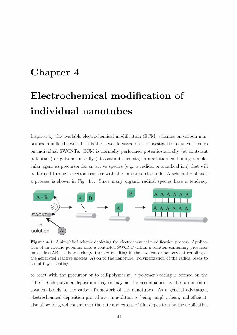
Chapter 4
Electrochemical modification of
individual nanotubes
Inspired by the available electrochemical modification (ECM) schemes on carbon nan-
otubes in bulk, the work in this thesis was focussed on the investigation of such schemes
on individual SWCNTs. ECM is normally performed potentiostatically (at contstant
potentials) or galvanostatically (at constant currents) in a solution containing a mole-
cular agent as precursor for an active species (e.g., a radical or a radical ion) that will
be formed through electron transfer with the nanotube electrode. A schematic of such
a process is shown in Fig. 4.1. Since many organic radical species have a tendency
Figure 4.1: A simplified scheme depicting the electrochemical modification process. Applica-tion of an electric potential onto a contacted SWCNT within a solution containing precursormolecules (AB) leads to a charge transfer resulting in the covalent or non-covlent coupling ofthe generated reactive species (A) on to the nanotube. Polymerization of the radical leads toa multilayer coating.
to react with the precursor or to self-polymerize, a polymer coating is formed on the
tubes. Such polymer deposition may or may not be accompanied by the formation of
covalent bonds to the carbon framework of the nanotubes. As a general advantage,
electrochemical deposition procedures, in addition to being simple, clean, and efficient,
also allow for good control over the rate and extent of film deposition by the application
41

42 CHAPTER 4. ELECTROCHEMICAL MODIFICATION
of appropriate electrochemical conditions such as duration and magnitude of the applied
potential. Furthermore, the use of a suitable agent containing the required substituent
enables one to tailor the chemical and physical properties of the resulting film.
This chapter starts with a short description of the experimental setup used for elec-
trochemical modification. This is followed by a discussion of two different coupling
schemes used in this work, namely oxidative and reductive ECM. The characterization
of individual SWCNTs modified by these two schemes is then presented. The next sec-
tion details the selective electrochemical modification of exclusively the m-SWCNTs in
an ensemble to obtain all–semiconducting networks that can be operated as FETs. The
chapter concludes with a collection of potential experiments for future work.
4.1 Instrumentation
The electrochemical experiments were carried out in a micro cell of capacity ≈ 500 µL
(see Fig. 4.2). The cell is made of teflon and comprises of platinum counter and
pseudoreference electrodes. A tungsten needle probe was used to make contact with
the electrodes on the substrate surface, which enabled the functioning of SWCNTs as
the working electrode. For the control of the potential that is applied to the SWCNTs
Figure 4.2: A mini-electrochemical cell used for performing electrochemical modification onindividually contacted SWCNTs. The counter and reference electrodes are made of platinumand a tungsten probe needle is used to contact the electrodes connected to the SWCNT. Thecell has a capacity of 500 µL.
through the working electrode and for monitoring the resulting current through the
electrochemical cell a Solartron 1285 potentiostat was used.
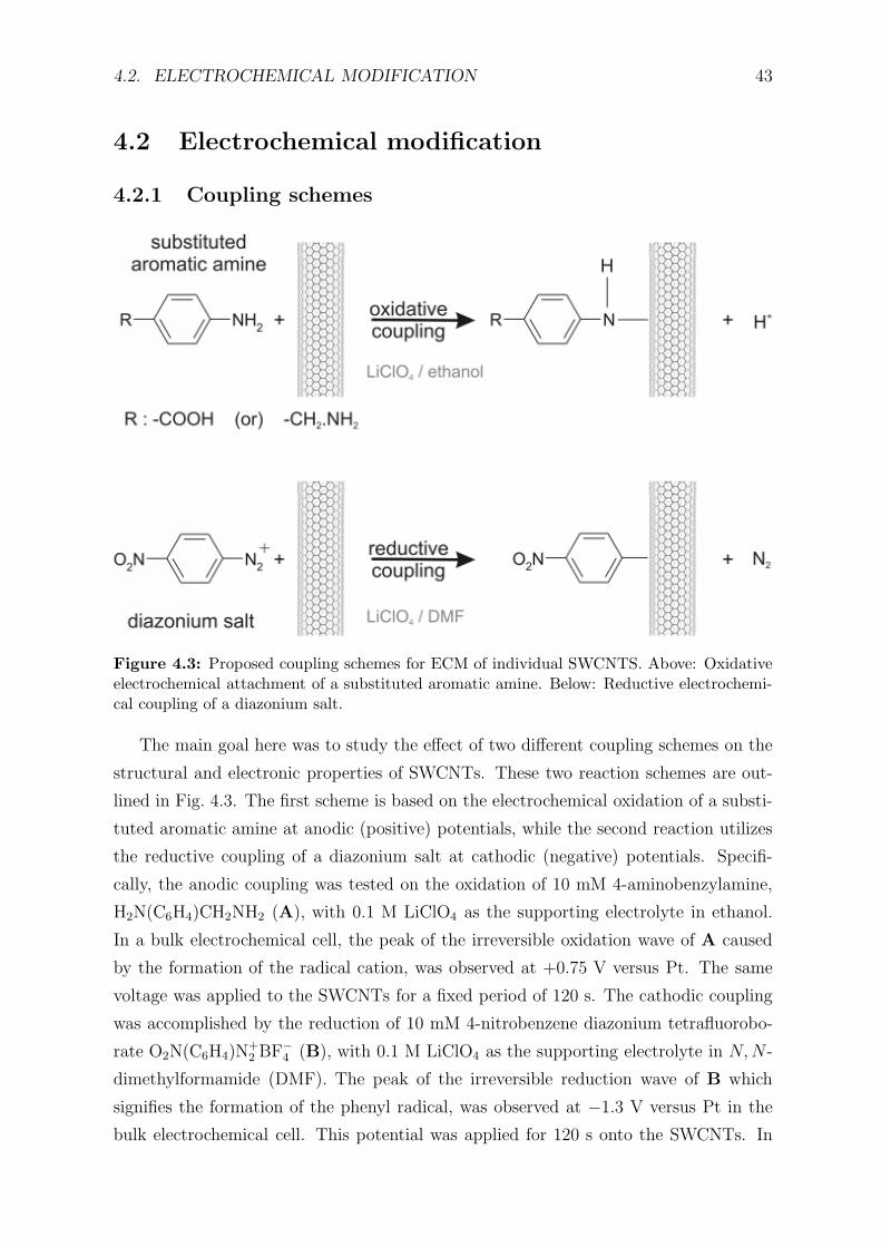
4.2. ELECTROCHEMICAL MODIFICATION 43
4.2 Electrochemical modification
4.2.1 Coupling schemes
Figure 4.3: Proposed coupling schemes for ECM of individual SWCNTS. Above: Oxidativeelectrochemical attachment of a substituted aromatic amine. Below: Reductive electrochemi-cal coupling of a diazonium salt.
The main goal here was to study the effect of two different coupling schemes on the
structural and electronic properties of SWCNTs. These two reaction schemes are out-
lined in Fig. 4.3. The first scheme is based on the electrochemical oxidation of a substi-
tuted aromatic amine at anodic (positive) potentials, while the second reaction utilizes
the reductive coupling of a diazonium salt at cathodic (negative) potentials. Specifi-
cally, the anodic coupling was tested on the oxidation of 10 mM 4-aminobenzylamine,
H2N(C6H4)CH2NH2 (A), with 0.1 M LiClO4 as the supporting electrolyte in ethanol.
In a bulk electrochemical cell, the peak of the irreversible oxidation wave of A caused
by the formation of the radical cation, was observed at +0.75 V versus Pt. The same
voltage was applied to the SWCNTs for a fixed period of 120 s. The cathodic coupling
was accomplished by the reduction of 10 mM 4-nitrobenzene diazonium tetrafluorobo-
rate O2N(C6H4)N+2 BF−
4 (B), with 0.1 M LiClO4 as the supporting electrolyte in N, N -
dimethylformamide (DMF). The peak of the irreversible reduction wave of B which
signifies the formation of the phenyl radical, was observed at −1.3 V versus Pt in the
bulk electrochemical cell. This potential was applied for 120 s onto the SWCNTs. In
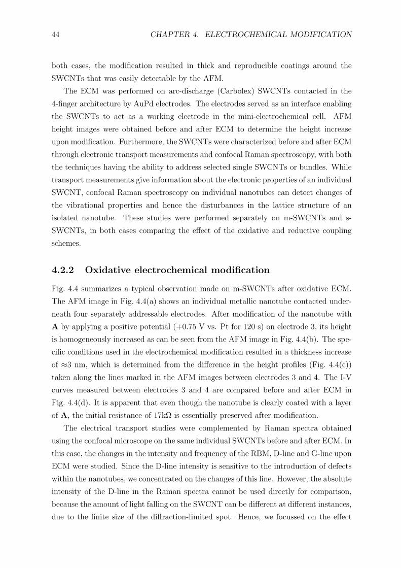
44 CHAPTER 4. ELECTROCHEMICAL MODIFICATION
both cases, the modification resulted in thick and reproducible coatings around the
SWCNTs that was easily detectable by the AFM.
The ECM was performed on arc-discharge (Carbolex) SWCNTs contacted in the
4-finger architecture by AuPd electrodes. The electrodes served as an interface enabling
the SWCNTs to act as a working electrode in the mini-electrochemical cell. AFM
height images were obtained before and after ECM to determine the height increase
upon modification. Furthermore, the SWCNTs were characterized before and after ECM
through electronic transport measurements and confocal Raman spectroscopy, with both
the techniques having the ability to address selected single SWCNTs or bundles. While
transport measurements give information about the electronic properties of an individual
SWCNT, confocal Raman spectroscopy on individual nanotubes can detect changes of
the vibrational properties and hence the disturbances in the lattice structure of an
isolated nanotube. These studies were performed separately on m-SWCNTs and s-
SWCNTs, in both cases comparing the effect of the oxidative and reductive coupling
schemes.
4.2.2 Oxidative electrochemical modification
Fig. 4.4 summarizes a typical observation made on m-SWCNTs after oxidative ECM.
The AFM image in Fig. 4.4(a) shows an individual metallic nanotube contacted under-
neath four separately addressable electrodes. After modification of the nanotube with
A by applying a positive potential (+0.75 V vs. Pt for 120 s) on electrode 3, its height
is homogeneously increased as can be seen from the AFM image in Fig. 4.4(b). The spe-
cific conditions used in the electrochemical modification resulted in a thickness increase
of ≈3 nm, which is determined from the difference in the height profiles (Fig. 4.4(c))
taken along the lines marked in the AFM images between electrodes 3 and 4. The I-V
curves measured between electrodes 3 and 4 are compared before and after ECM in
Fig. 4.4(d). It is apparent that even though the nanotube is clearly coated with a layer
of A, the initial resistance of 17kΩ is essentially preserved after modification.
The electrical transport studies were complemented by Raman spectra obtained
using the confocal microscope on the same individual SWCNTs before and after ECM. In
this case, the changes in the intensity and frequency of the RBM, D-line and G-line upon
ECM were studied. Since the D-line intensity is sensitive to the introduction of defects
within the nanotubes, we concentrated on the changes of this line. However, the absolute
intensity of the D-line in the Raman spectra cannot be used directly for comparison,
because the amount of light falling on the SWCNT can be different at different instances,
due to the finite size of the diffraction-limited spot. Hence, we focussed on the effect
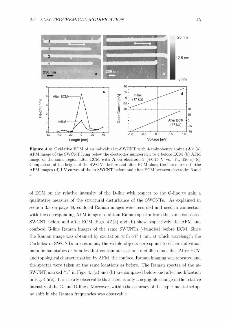
4.2. ELECTROCHEMICAL MODIFICATION 45
Figure 4.4: Oxidative ECM of an individual m-SWCNT with 4-aminobenzylamine (A): (a)AFM image of the SWCNT lying below the electrodes numbered 1 to 4 before ECM (b) AFMimage of the same region after ECM with A on electrode 3 (+0.75 V vs. Pt, 120 s) (c)Comparison of the height of the SWCNT before and after ECM along the line marked in theAFM images (d) I-V curves of the m-SWCNT before and after ECM between electrodes 3 and4.
of ECM on the relative intensity of the D-line with respect to the G-line to gain a
qualitative measure of the structural disturbance of the SWCNTs. As explained in
section 3.3 on page 39, confocal Raman images were recorded and used in connection
with the corresponding AFM images to obtain Raman spectra from the same contacted
SWCNT before and after ECM. Figs. 4.5(a) and (b) show respectively the AFM and
confocal G-line Raman images of the same SWCNTs (-bundles) before ECM. Since
the Raman image was obtained by excitation with 647.1 nm, at which wavelength the
Carbolex m-SWCNTs are resonant, the visible objects correspond to either individual
metallic nanotubes or bundles that contain at least one metallic nanotube. After ECM
and topological characterization by AFM, the confocal Raman imaging was repeated and
the spectra were taken at the same locations as before. The Raman spectra of the m-
SWCNT marked “x” in Figs. 4.5(a) and (b) are compared before and after modification
in Fig. 4.5(c). It is clearly observable that there is only a negligible change in the relative
intensity of the G- and D-lines. Moreover, within the accuracy of the experimental setup,
no shift in the Raman frequencies was observable.
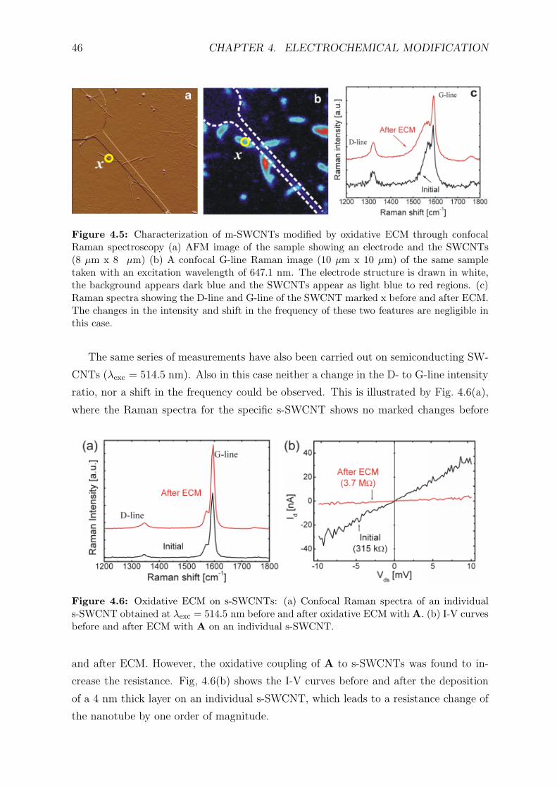
46 CHAPTER 4. ELECTROCHEMICAL MODIFICATION
Figure 4.5: Characterization of m-SWCNTs modified by oxidative ECM through confocalRaman spectroscopy (a) AFM image of the sample showing an electrode and the SWCNTs(8 µm x 8 µm) (b) A confocal G-line Raman image (10 µm x 10 µm) of the same sampletaken with an excitation wavelength of 647.1 nm. The electrode structure is drawn in white,the background appears dark blue and the SWCNTs appear as light blue to red regions. (c)Raman spectra showing the D-line and G-line of the SWCNT marked x before and after ECM.The changes in the intensity and shift in the frequency of these two features are negligible inthis case.
The same series of measurements have also been carried out on semiconducting SW-
CNTs (λexc = 514.5 nm). Also in this case neither a change in the D- to G-line intensity
ratio, nor a shift in the frequency could be observed. This is illustrated by Fig. 4.6(a),
where the Raman spectra for the specific s-SWCNT shows no marked changes before
Figure 4.6: Oxidative ECM on s-SWCNTs: (a) Confocal Raman spectra of an individuals-SWCNT obtained at λexc = 514.5 nm before and after oxidative ECM with A. (b) I-V curvesbefore and after ECM with A on an individual s-SWCNT.
and after ECM. However, the oxidative coupling of A to s-SWCNTs was found to in-
crease the resistance. Fig, 4.6(b) shows the I-V curves before and after the deposition
of a 4 nm thick layer on an individual s-SWCNT, which leads to a resistance change of
the nanotube by one order of magnitude.
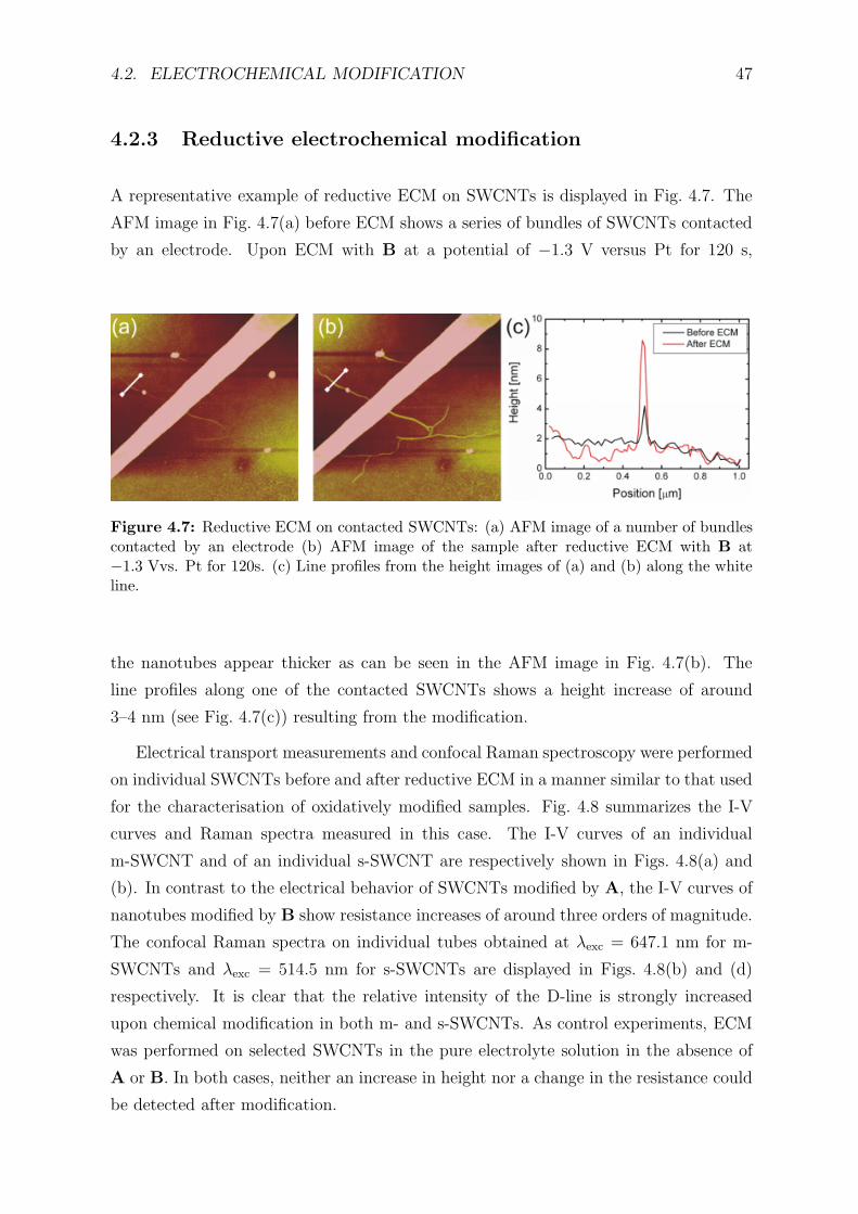
4.2. ELECTROCHEMICAL MODIFICATION 47
4.2.3 Reductive electrochemical modification
A representative example of reductive ECM on SWCNTs is displayed in Fig. 4.7. The
AFM image in Fig. 4.7(a) before ECM shows a series of bundles of SWCNTs contacted
by an electrode. Upon ECM with B at a potential of −1.3 V versus Pt for 120 s,
Figure 4.7: Reductive ECM on contacted SWCNTs: (a) AFM image of a number of bundlescontacted by an electrode (b) AFM image of the sample after reductive ECM with B at−1.3 Vvs. Pt for 120s. (c) Line profiles from the height images of (a) and (b) along the whiteline.
the nanotubes appear thicker as can be seen in the AFM image in Fig. 4.7(b). The
line profiles along one of the contacted SWCNTs shows a height increase of around
3–4 nm (see Fig. 4.7(c)) resulting from the modification.
Electrical transport measurements and confocal Raman spectroscopy were performed
on individual SWCNTs before and after reductive ECM in a manner similar to that used
for the characterisation of oxidatively modified samples. Fig. 4.8 summarizes the I-V
curves and Raman spectra measured in this case. The I-V curves of an individual
m-SWCNT and of an individual s-SWCNT are respectively shown in Figs. 4.8(a) and
(b). In contrast to the electrical behavior of SWCNTs modified by A, the I-V curves of
nanotubes modified by B show resistance increases of around three orders of magnitude.
The confocal Raman spectra on individual tubes obtained at λexc = 647.1 nm for m-
SWCNTs and λexc = 514.5 nm for s-SWCNTs are displayed in Figs. 4.8(b) and (d)
respectively. It is clear that the relative intensity of the D-line is strongly increased
upon chemical modification in both m- and s-SWCNTs. As control experiments, ECM
was performed on selected SWCNTs in the pure electrolyte solution in the absence of
A or B. In both cases, neither an increase in height nor a change in the resistance could
be detected after modification.
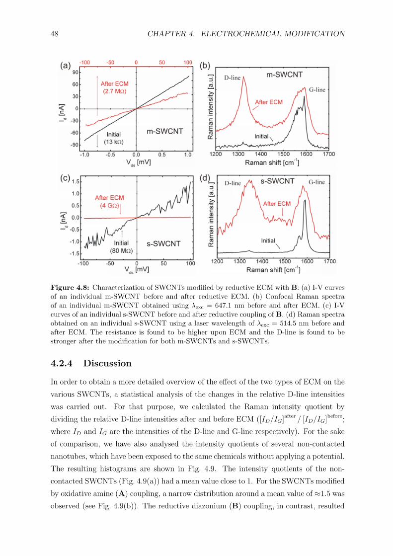
48 CHAPTER 4. ELECTROCHEMICAL MODIFICATION
Figure 4.8: Characterization of SWCNTs modified by reductive ECM with B: (a) I-V curvesof an individual m-SWCNT before and after reductive ECM. (b) Confocal Raman spectraof an individual m-SWCNT obtained using λexc = 647.1 nm before and after ECM. (c) I-Vcurves of an individual s-SWCNT before and after reductive coupling of B. (d) Raman spectraobtained on an individual s-SWCNT using a laser wavelength of λexc = 514.5 nm before andafter ECM. The resistance is found to be higher upon ECM and the D-line is found to bestronger after the modification for both m-SWCNTs and s-SWCNTs.
4.2.4 Discussion
In order to obtain a more detailed overview of the effect of the two types of ECM on the
various SWCNTs, a statistical analysis of the changes in the relative D-line intensities
was carried out. For that purpose, we calculated the Raman intensity quotient by
dividing the relative D-line intensities after and before ECM ([ID/IG]after / [ID/IG]before;
where ID and IG are the intensities of the D-line and G-line respectively). For the sake
of comparison, we have also analysed the intensity quotients of several non-contacted
nanotubes, which have been exposed to the same chemicals without applying a potential.
The resulting histograms are shown in Fig. 4.9. The intensity quotients of the non-
contacted SWCNTs (Fig. 4.9(a)) had a mean value close to 1. For the SWCNTs modified
by oxidative amine (A) coupling, a narrow distribution around a mean value of ≈1.5 was
observed (see Fig. 4.9(b)). The reductive diazonium (B) coupling, in contrast, resulted
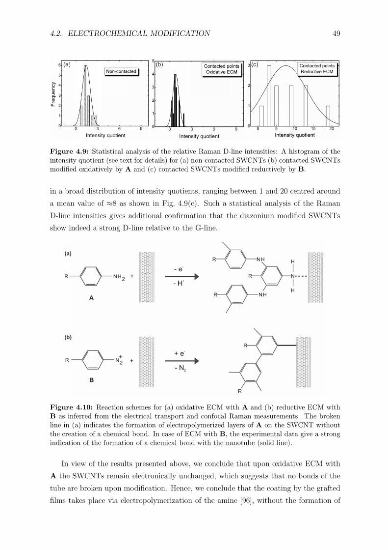
4.2. ELECTROCHEMICAL MODIFICATION 49
Figure 4.9: Statistical analysis of the relative Raman D-line intensities: A histogram of theintensity quotient (see text for details) for (a) non-contacted SWCNTs (b) contacted SWCNTsmodified oxidatively by A and (c) contacted SWCNTs modified reductively by B.
in a broad distribution of intensity quotients, ranging between 1 and 20 centred around
a mean value of ≈8 as shown in Fig. 4.9(c). Such a statistical analysis of the Raman
D-line intensities gives additional confirmation that the diazonium modified SWCNTs
show indeed a strong D-line relative to the G-line.
Figure 4.10: Reaction schemes for (a) oxidative ECM with A and (b) reductive ECM withB as inferred from the electrical transport and confocal Raman measurements. The brokenline in (a) indicates the formation of electropolymerized layers of A on the SWCNT withoutthe creation of a chemical bond. In case of ECM with B, the experimental data give a strongindication of the formation of a chemical bond with the nanotube (solid line).
In view of the results presented above, we conclude that upon oxidative ECM with
A the SWCNTs remain electronically unchanged, which suggests that no bonds of the
tube are broken upon modification. Hence, we conclude that the coating by the grafted
films takes place via electropolymerization of the amine [96], without the formation of
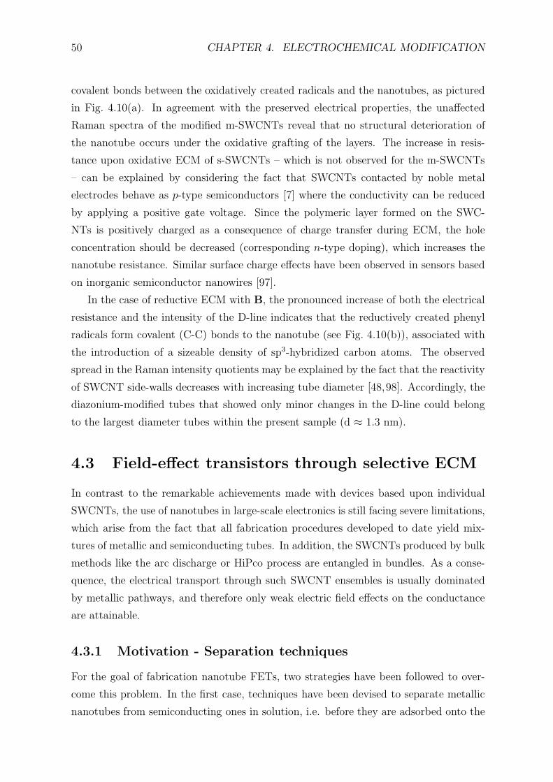
50 CHAPTER 4. ELECTROCHEMICAL MODIFICATION
covalent bonds between the oxidatively created radicals and the nanotubes, as pictured
in Fig. 4.10(a). In agreement with the preserved electrical properties, the unaffected
Raman spectra of the modified m-SWCNTs reveal that no structural deterioration of
the nanotube occurs under the oxidative grafting of the layers. The increase in resis-
tance upon oxidative ECM of s-SWCNTs – which is not observed for the m-SWCNTs
– can be explained by considering the fact that SWCNTs contacted by noble metal
electrodes behave as p-type semiconductors [7] where the conductivity can be reduced
by applying a positive gate voltage. Since the polymeric layer formed on the SWC-
NTs is positively charged as a consequence of charge transfer during ECM, the hole
concentration should be decreased (corresponding n-type doping), which increases the
nanotube resistance. Similar surface charge effects have been observed in sensors based
on inorganic semiconductor nanowires [97].
In the case of reductive ECM with B, the pronounced increase of both the electrical
resistance and the intensity of the D-line indicates that the reductively created phenyl
radicals form covalent (C-C) bonds to the nanotube (see Fig. 4.10(b)), associated with
the introduction of a sizeable density of sp3-hybridized carbon atoms. The observed
spread in the Raman intensity quotients may be explained by the fact that the reactivity
of SWCNT side-walls decreases with increasing tube diameter [48,98]. Accordingly, the
diazonium-modified tubes that showed only minor changes in the D-line could belong
to the largest diameter tubes within the present sample (d ≈ 1.3 nm).
4.3 Field-effect transistors through selective ECM
In contrast to the remarkable achievements made with devices based upon individual
SWCNTs, the use of nanotubes in large-scale electronics is still facing severe limitations,
which arise from the fact that all fabrication procedures developed to date yield mix-
tures of metallic and semiconducting tubes. In addition, the SWCNTs produced by bulk
methods like the arc discharge or HiPco process are entangled in bundles. As a conse-
quence, the electrical transport through such SWCNT ensembles is usually dominated
by metallic pathways, and therefore only weak electric field effects on the conductance
are attainable.
4.3.1 Motivation - Separation techniques
For the goal of fabrication nanotube FETs, two strategies have been followed to over-
come this problem. In the first case, techniques have been devised to separate metallic
nanotubes from semiconducting ones in solution, i.e. before they are adsorbed onto the
4.3. FIELD-EFFECT TRANSISTORS THROUGH SELECTIVE ECM 51
substrate. Dispersing a SWCNT soot with octadecylamine (ODA) in tetrahydrofuran
is expected to result in a physisorbed coating of ODA onto the sidewalls of s-SWCNTs
due to the higher affinity of the latter to ODA [12]. The m-SWCNTs could then be
separated by precipitation. In a similar experiment, SWCNTs have been dispersed with
single stranded DNA yelding nanotubes wrapped with DNA molecules [15]. Anion ex-
change chromatography has been subsequently used to extract an enriched fraction of
metallic tubes utililizing the difference in surface charge between the DNA-metallic and
the DNA-semiconducting SWCNTs. Another method relies on the increased capabil-
ity of charge-transfer complex formation by bromine with the m-SWCNTs, resulting in
the ability to separate one type from the other just by using centrifugation [13]. Re-
cently, it has been demonstrated that the varying dielectric constants of the metallic
and semiconducting tubes could be utilized in separating the m-SWCNTs alone from
a suspension through alternating current dielectrophoresis [14]. However, in all these
cases, no quantitive separation could be achieved.
The second kind of strategy utilizes the fact that the s-SWCNTs can be turned to
the insulating (OFF ) state by applying a positive gate voltage. By ramping the drain-
source voltage to sufficiently high potentials under the presence of oxygen, it is possible
to burn off the metallic nanotubes [16]. This approach, which has until now successfully
been applied to individual SWCNT bundles, has the disadvantage that the Joule heat
produced in the m-SWCNTs may strongly affect adjacent s-SWCNTs.
4.3.2 Selective ECM on bundles of SWCNTs
In this work, a novel method has been designed to fabricate SWCNT-FETs in a generic
manner, which extends the scope of the selective-destruction-approach. Specifically,
ECM is used to eliminate the current carrying capability of the m-SWCNTs within
an ensemble. As detailed in the previous section, this task is performed by electro-
chemically generating reactive phenyl radicals that are able to covalently attach in high
densities to the nanotube sidewall, leading to an increase in resistance by several orders
of magnitude. Selective reaction of the metallic tubes can be achieved after gate-induced
switching of the s-SWCNTs to the OFF state. This results in a purely semiconducting
SWCNT channel between source and drain electrodes. The major advantage of the
electrochemical approach is the creation of a reactive species directly at the surface of
the conducting tubes, which enables a highly localized functionalization.
The samples were fabricated using tubes from the HiPco process and contacted by
AuPd electrodes on top in the 1.3 µm gap configuration. The density of tubes was
chosen such that between 1 and 10 individual tubes or thin bundles connected the two
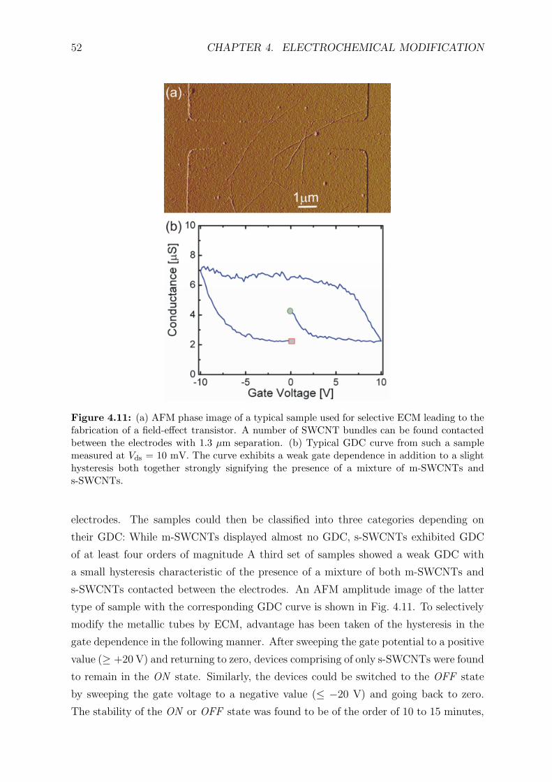
52 CHAPTER 4. ELECTROCHEMICAL MODIFICATION
Figure 4.11: (a) AFM phase image of a typical sample used for selective ECM leading to thefabrication of a field-effect transistor. A number of SWCNT bundles can be found contactedbetween the electrodes with 1.3 µm separation. (b) Typical GDC curve from such a samplemeasured at Vds = 10 mV. The curve exhibits a weak gate dependence in addition to a slighthysteresis both together strongly signifying the presence of a mixture of m-SWCNTs ands-SWCNTs.
electrodes. The samples could then be classified into three categories depending on
their GDC: While m-SWCNTs displayed almost no GDC, s-SWCNTs exhibited GDC
of at least four orders of magnitude A third set of samples showed a weak GDC with
a small hysteresis characteristic of the presence of a mixture of both m-SWCNTs and
s-SWCNTs contacted between the electrodes. An AFM amplitude image of the latter
type of sample with the corresponding GDC curve is shown in Fig. 4.11. To selectively
modify the metallic tubes by ECM, advantage has been taken of the hysteresis in the
gate dependence in the following manner. After sweeping the gate potential to a positive
value (≥ +20 V) and returning to zero, devices comprising of only s-SWCNTs were found
to remain in the ON state. Similarly, the devices could be switched to the OFF state
by sweeping the gate voltage to a negative value (≤ −20 V) and going back to zero.
The stability of the ON or OFF state was found to be of the order of 10 to 15 minutes,

4.3. FIELD-EFFECT TRANSISTORS THROUGH SELECTIVE ECM 53
sufficient to perform ECM with the semiconducting tubes in the OFF state without the
need for in-situ gate control.
In order to optimize the parameters of the ECM (for e.g. the concentration of the
diazonium salt, the magnitude and duration of the applied potential) with respect to
maximal preservation of the semiconducting nanotubes, control studies were initially
Figure 4.12: Room-temperature GDC curves of (a) a pure s-SWCNT: initial (black line),after OFF state ECM (red line) and after ON state ECM (blue line). (b) a m-SWCNT bundle:initial (black) and after OFF state ECM (red). The parameters of ECM were: −280 mV vs.Pt for 30 s in 10 mM B. Vdswas 100 mV in (a) and 1 mV before ECM and 100 mV after ECMin (b).
carried out with pure semiconducting and pure metallic tubes after gate tuning. It is
noteworthy that in order to obtain reproducible results, the samples were heated at
100C for 2 h immediately after ECM, to ensure removal of physisorbed solvent mole-
cules. The application of −280 mV versus Pt for 30 s in a 10 mM 4-nitrobenzene
diazonium salt (B) solution in N, N -dimethylformamide (DMF), with 0.1 M LiClO4 as
background electrolyte was found to cause only minor changes in the conductance of an
individual semiconducting nanotube in the OFF state, as demonstrated by Fig. 4.12(a).

54 CHAPTER 4. ELECTROCHEMICAL MODIFICATION
Here the black curve is the initial gate dependence of conductance, while the red curve
corresponds to the gate dependence after ECM in the OFF state. On the contrary,
after subjecting the same semiconducting SWCNT in the ON state to ECM (blue line
in Fig. 4.12(a)), the conductance reduced by four orders of magnitude for all gate volt-
ages. To test whether the metallic SWCNTs are indeed modified under the OFF state
conditions of the semiconducting tubes, the same parameters were applied to a purely
metallic SWCNT bundle. In general, the modified metallic tubes showed a strong in-
crease in resistance, as exemplified in Fig. 4.12(b) where the conductance is seen to drop
by four orders of magnitude.
The same methodology was then applied to ensembles of SWCNTs containing a
mixture of both m- and s-SWCNTs. For this purpose, a sample with few contacted
bundles was taken. This bundle displayed a weak gate dependence of conductance, as
apparent from Fig. 4.13 (black curve). After ECM in the OFF state, the bundle thick-
ness was found to be slightly increased, which results from the formation of a molecular
coating due to polymerisation of the electrochemically generated phenyl radicals at the
Figure 4.13: Creation of an FET through selective ECM of SWCNT bundles: Room-temperature GDC curves of the sample before ECM (black curve) showing a weak gate de-pendence (ON /OFF ratio) of 3, indicating the presence of both m-SWCNTs and s-SWCNTs.The red curve is obtained after OFF state ECM and the device now exhibits a switching ratioof 8 x 10⁵. Vds was 10 mV before ECM and 50 mV after ECM.
SWCNT/electrolyte interface. Most strikingly, the gate dependence of conductance of
the modified bundle (shown by the red line in Fig. 4.13) displays a significant increase
in the ON to OFF ratio from 3 before modification to ≈106 afterwards. The shape of
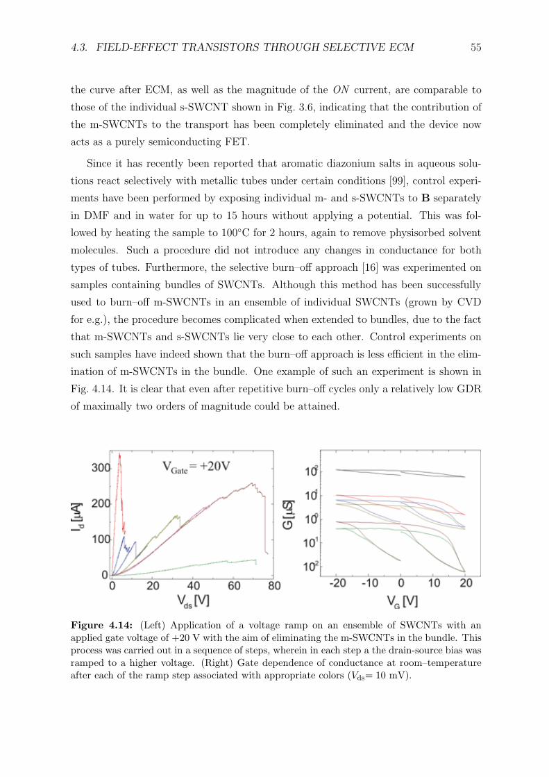
4.3. FIELD-EFFECT TRANSISTORS THROUGH SELECTIVE ECM 55
the curve after ECM, as well as the magnitude of the ON current, are comparable to
those of the individual s-SWCNT shown in Fig. 3.6, indicating that the contribution of
the m-SWCNTs to the transport has been completely eliminated and the device now
acts as a purely semiconducting FET.
Since it has recently been reported that aromatic diazonium salts in aqueous solu-
tions react selectively with metallic tubes under certain conditions [99], control experi-
ments have been performed by exposing individual m- and s-SWCNTs to B separately
in DMF and in water for up to 15 hours without applying a potential. This was fol-
lowed by heating the sample to 100C for 2 hours, again to remove physisorbed solvent
molecules. Such a procedure did not introduce any changes in conductance for both
types of tubes. Furthermore, the selective burn–off approach [16] was experimented on
samples containing bundles of SWCNTs. Although this method has been successfully
used to burn–off m-SWCNTs in an ensemble of individual SWCNTs (grown by CVD
for e.g.), the procedure becomes complicated when extended to bundles, due to the fact
that m-SWCNTs and s-SWCNTs lie very close to each other. Control experiments on
such samples have indeed shown that the burn–off approach is less efficient in the elim-
ination of m-SWCNTs in the bundle. One example of such an experiment is shown in
Fig. 4.14. It is clear that even after repetitive burn–off cycles only a relatively low GDR
of maximally two orders of magnitude could be attained.
Figure 4.14: (Left) Application of a voltage ramp on an ensemble of SWCNTs with anapplied gate voltage of +20 V with the aim of eliminating the m-SWCNTs in the bundle. Thisprocess was carried out in a sequence of steps, wherein in each step a the drain-source bias wasramped to a higher voltage. (Right) Gate dependence of conductance at room–temperatureafter each of the ramp step associated with appropriate colors (Vds= 10 mV).
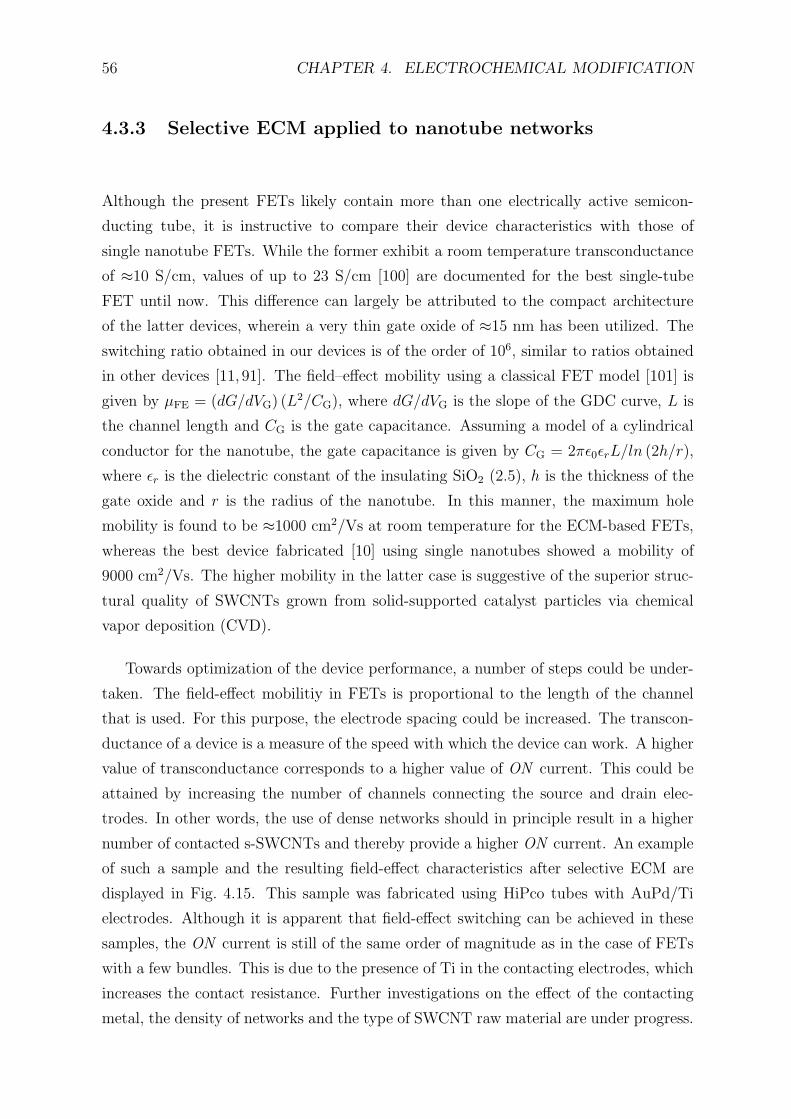
56 CHAPTER 4. ELECTROCHEMICAL MODIFICATION
4.3.3 Selective ECM applied to nanotube networks
Although the present FETs likely contain more than one electrically active semicon-
ducting tube, it is instructive to compare their device characteristics with those of
single nanotube FETs. While the former exhibit a room temperature transconductance
of ≈10 S/cm, values of up to 23 S/cm [100] are documented for the best single-tube
FET until now. This difference can largely be attributed to the compact architecture
of the latter devices, wherein a very thin gate oxide of ≈15 nm has been utilized. The
switching ratio obtained in our devices is of the order of 106, similar to ratios obtained
in other devices [11, 91]. The field–effect mobility using a classical FET model [101] is
given by µFE = (dG/dVG) (L2/CG), where dG/dVG is the slope of the GDC curve, L is
the channel length and CG is the gate capacitance. Assuming a model of a cylindrical
conductor for the nanotube, the gate capacitance is given by CG = 2πǫ0ǫrL/ln (2h/r),
where ǫr is the dielectric constant of the insulating SiO2 (2.5), h is the thickness of the
gate oxide and r is the radius of the nanotube. In this manner, the maximum hole
mobility is found to be ≈1000 cm2/Vs at room temperature for the ECM-based FETs,
whereas the best device fabricated [10] using single nanotubes showed a mobility of
9000 cm2/Vs. The higher mobility in the latter case is suggestive of the superior struc-
tural quality of SWCNTs grown from solid-supported catalyst particles via chemical
vapor deposition (CVD).
Towards optimization of the device performance, a number of steps could be under-
taken. The field-effect mobilitiy in FETs is proportional to the length of the channel
that is used. For this purpose, the electrode spacing could be increased. The transcon-
ductance of a device is a measure of the speed with which the device can work. A higher
value of transconductance corresponds to a higher value of ON current. This could be
attained by increasing the number of channels connecting the source and drain elec-
trodes. In other words, the use of dense networks should in principle result in a higher
number of contacted s-SWCNTs and thereby provide a higher ON current. An example
of such a sample and the resulting field-effect characteristics after selective ECM are
displayed in Fig. 4.15. This sample was fabricated using HiPco tubes with AuPd/Ti
electrodes. Although it is apparent that field-effect switching can be achieved in these
samples, the ON current is still of the same order of magnitude as in the case of FETs
with a few bundles. This is due to the presence of Ti in the contacting electrodes, which
increases the contact resistance. Further investigations on the effect of the contacting
metal, the density of networks and the type of SWCNT raw material are under progress.
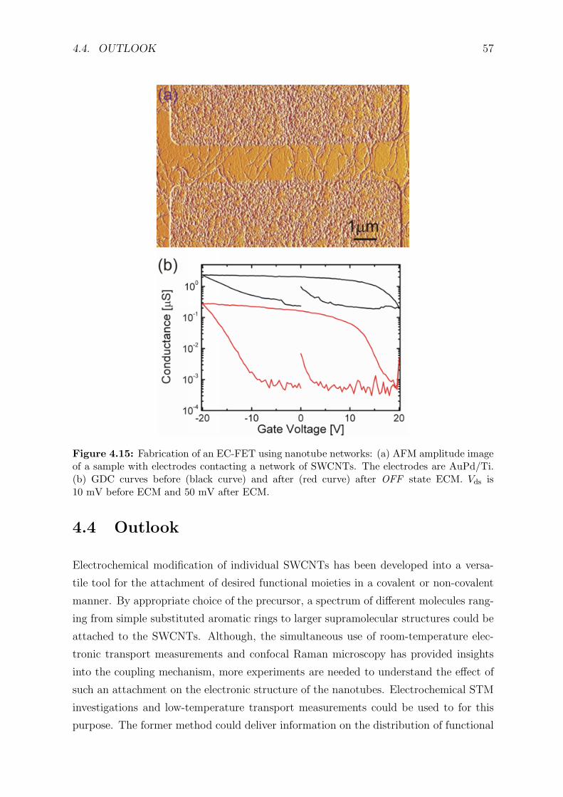
4.4. OUTLOOK 57
Figure 4.15: Fabrication of an EC-FET using nanotube networks: (a) AFM amplitude imageof a sample with electrodes contacting a network of SWCNTs. The electrodes are AuPd/Ti.(b) GDC curves before (black curve) and after (red curve) after OFF state ECM. Vds is10 mV before ECM and 50 mV after ECM.
4.4 Outlook
Electrochemical modification of individual SWCNTs has been developed into a versa-
tile tool for the attachment of desired functional moieties in a covalent or non-covalent
manner. By appropriate choice of the precursor, a spectrum of different molecules rang-
ing from simple substituted aromatic rings to larger supramolecular structures could be
attached to the SWCNTs. Although, the simultaneous use of room-temperature elec-
tronic transport measurements and confocal Raman microscopy has provided insights
into the coupling mechanism, more experiments are needed to understand the effect of
such an attachment on the electronic structure of the nanotubes. Electrochemical STM
investigations and low-temperature transport measurements could be used to for this
purpose. The former method could deliver information on the distribution of functional
58 CHAPTER 4. ELECTROCHEMICAL MODIFICATION
groups on tubes with sub-monolayer coatings.
On the other hand, from an application point of view, ECM is an elegant tool for the
fabrication of nano-scale electronic devices, as has been demonstrated in this work by
the selective electrochemical functionalization of m-SWCNTs contained within a nan-
otube network. ECM is also promising for the fabrication of chemical sensors. Due to
their large surface to volume ratio, individual pristine nanotubes show high sensitivites
for certain gases at room temperature [102]. However, for the detection of molecules
that are only weakly adsorbed (e.g. carbon monoxide and hydrogen), the change in re-
sistance is often too small. A possible workaround is accomplished by the modification
of the nanotube sidewalls through nanoparticles made of a suitable metal. For instance,
sensitive hydrogen sensors operating at room temperature have been fabricated via
electro-deposition of palladium nanoparticles [3]. Individual SWCNTs modified electro-
chemically by appropriate functional groups are also attractive for detecting ions (pH)
in aqueous solutions. One strategy that could be employed here is the introduction of
covalently bonded molecules containing pH-sensitive groups. The moieties introduced
in such a manner may behave as pH-dependent scattering sites, so that the resistance
of the nanotube would be a direct indicator of the pH of the solution. Future studies
could also involve the attachment of ligand- or receptorlike functionalities that offers the
potential of producing nanowires that are compatible with biological structural motifs
for applications such as the contacting of nerve cells on a solid support.

Chapter 5
Photoelectronic transport
properties of individual nanotubes
SWCNTs are evolving to be a promising candidate as components of nano-scale elec-
tronic devices. Towards fabrication of such molecular electronics devices, a detailed
understanding of the electronic transport through SWCNTs is essential. The effect of
the environment, the type of the contacts, the presence of structural inhomogeneities as
well as the type of raw material used all have a crucial impact on the electronic transport
behaviour of the nanotubes. A complete understanding of the influence of these factors
on the electrical properties of SWCNTs is, however, still in its infancy. While various
techniques have been utilized in the study of the transport properties in dark, much less
is known about their photoelectronic transport (PET) properties. The investigation of
electronic transport under the influence of photo-illumination helps in understanding
these effects to a great extent. Thus a study of the PET properties of individual nan-
otubes has important implications for future nano-scale optoelectronic and photovoltaic
devices. This chapter starts with a short description of the current status of investiga-
tions on photoelectronic transport in SWCNTs. This is followed by a short sketch of
the two experimental setups that have been used during this work. Subsequently the
PET investigations on individual s-SWCNTs and m-SWCNTs are presented separately
and the chapter concludes with an outlook of potential future experiments.
5.1 Photoelectronic transport – Background
The first ever experiments on the PET properties of SWCNTs were performed by Fuji-
wara et al. [18], who used thin films of SWCNT bundles obtained from the arc discharge
process. The thickness of the films ranged from 300 to 500 nm and were contacted
59
60 CHAPTER 5. PHOTOELECTRONIC TRANSPORT
directly by gold electrodes separated 10 µm apart. The whole sample was illuminated
with a pulsed laser whose energy could be tuned in the range of 0.5 eV to 2.8 eV. The
photocurrent at room temperature showed two strong peaks for excitation at 0.7 eV and
1.2 eV, in agreement with the first two interband transitions Es11 and Es
22 for arc-
discharge tubes having a diameter of ≈ 1.4 nm. The effect of the presence of other
metallic tubes in such a film was not discussed here, probably because the fraction of
s-SWCNTs in the film was quite high due to the sharp diameter distribution of these
samples. In another experiment with SWCNT films of similar thickness and electrode
spacings varying from 15 to 300 µm, photoconductivity could be observed at near infra-
red wavelengths corresponding to an energy of ≈ 1.46 eV [103]. The diameters of the
SWCNTs were however in a broader range of 0.8 to 1.1 nm. The samples exhibited a
slow response of the photocurrent towards illumination, which they attributed to the
sorption of oxygen onto the SWCNT films.
The mechanism of photoconductivity observed in the above experiments was not
really clear due to the investigation of a mixture containing both m-SWCNTs and s-
SWCNTs. The PET properties of an individual s-SWCNT was first studied by Chen
et al. [42], who used a CVD–grown tube with a diameter of 1.5 nm and contacted by
electrodes spaced by ≈1.5 µm. An ultraviolet (UV) light source with a wavelength of
λexc = 254 nm (4.9 eV) and a low power intensity of 2 mW/cm2 was utilized here.
A decrease in conductance was observed upon global illumination of these samples,
which was traced back to photoinduced desorption of oxygen from the surface of the
s-SWCNT. It has been shown previously that under ambient conditions, oxygen adsorbs
onto the SWCNTs and dopes them by withdrawing one tenth of an electron per oxygen
molecule [104,105], as a result of which s-SWCNTs behave as p-type semiconductors in
air. Under UV illumination, oxygen photodesorption causes a reduction of hole carriers,
thus lowering the sample conductance. Furthermore, the high energy of illumination
(4.9 eV) is quite close to the work function of the s-SWCNT (≈ 5 eV for a s-SWCNTof
diameter 1.5 nm), as obtained by first principles calculations [106]. Thus, the pho-
toexcited electrons have a high probability of inducing such a desorption process. A
wavelength dependence of this photoeffect indicated that photodesorption is maximum
at high energies and reduces drastically when moving down to lower excitation energies.
They also observed such a phenomenon using a SWCNT film sample. Ruling out the
possibility of photocurrent generation, they attributed photoinduced excitation of plas-
mons as the cause for the photodesorption of adsorbed molecules. There appear two
plausible reasons why photoconductivity could not be observed in this experiment. The
first one probably relates to the chosen wavelength where molecular photodesorption ef-
5.2. INSTRUMENTATION 61
fects are dominant. The second reason could be the illumination of the sample at a high
current state of the s-SWCNT. At VG = 0 V, the s-SWCNT was in its high conductance
state. In such a situation, the holes in the valence band contribute to the flow of cur-
rent through the device. The photoinduced carriers then form only a small fraction of
the current-carrying holes and hence it was not possible to measure the photogenerated
current in this experiment.
Incorporating this aspect and switching the device to the low conductance or
OFF state, it was indeed possible to measure true photoconductivity through an individ-
ual s-SWCNT [21]. Here, the ambipolar device comprised of an individual s-SWCNT of
diameter ≈ 1.3 nm obtained using the laser ablation procedure. The electrodes were
made of Ti spaced ≈ 800 nm apart and the device was protected from the effect of
surroundings by a 10 nm SiO2 layer. The s-SWCNT was also illuminated globally using
a laser tunable in the energy range of 1.27 to 1.59 eV and a maximum power intensity
of 10 kW/cm2. The photocurrent showed a linear dependence on the power intensity
and was maximum for the polarization of light being parallel to the orientation of the
tube. At 0.6 V, ≈ 3pA/( kW/cm2) of photocurrent could be observed corresponding to
a photoconductance of ≈ 5pS/( kW/cm2). The authors proposed a mechanism wherein
the incident infrared light excited the second exciton state Es22 of the s-SWCNT fol-
lowed by the decay of the excited state to an electron hole pair at the band edge which
then drifts under application of an electric field. Although this experiment enabled the
observation of photoconductivity the local origin of the generation of the photocurrent
could not be explored. The experiments performed in this work show for the first time
the effect of localized photo-excitation on the electronic transport through individual
SWCNTs.
5.2 Instrumentation
The heart of the experimental setup comprises of a focussed laser beam from the confocal
microscope (refer to section 3.3) to enable local illumination of an individual SWCNT.
This setup has been coupled with the arrangement for electronic transport measurement,
which in turn facilitates the investigation of photoinduced electronic transport at a local
scale. A block diagram of the measurement setup is displayed in Fig. 5.1. The relatively
small extension of the laser spot opens up the possibility to record the photocurrent
signal that originates from illumination at different locations along a contacted SWCNT.
When this photocurrent is plotted as a function of position, an image of the photocurrent
similar to a confocal reflection or Raman image is obtained. This image is termed as a
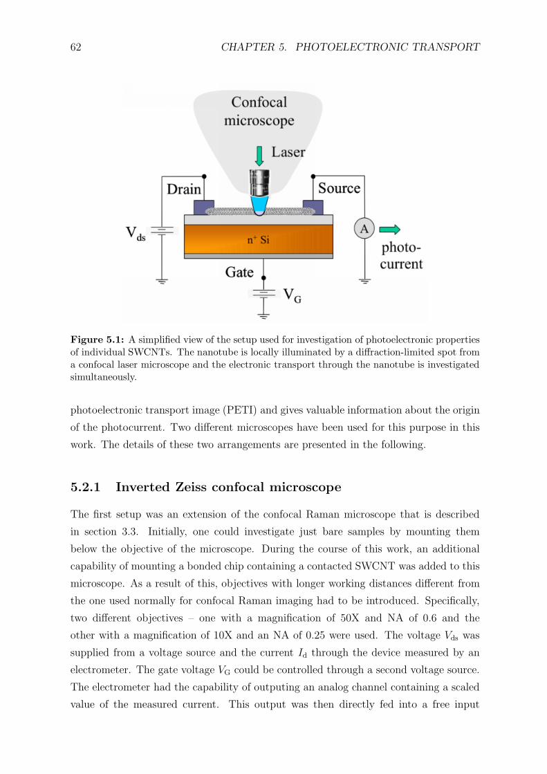
62 CHAPTER 5. PHOTOELECTRONIC TRANSPORT
Figure 5.1: A simplified view of the setup used for investigation of photoelectronic propertiesof individual SWCNTs. The nanotube is locally illuminated by a diffraction-limited spot froma confocal laser microscope and the electronic transport through the nanotube is investigatedsimultaneously.
photoelectronic transport image (PETI) and gives valuable information about the origin
of the photocurrent. Two different microscopes have been used for this purpose in this
work. The details of these two arrangements are presented in the following.
5.2.1 Inverted Zeiss confocal microscope
The first setup was an extension of the confocal Raman microscope that is described
in section 3.3. Initially, one could investigate just bare samples by mounting them
below the objective of the microscope. During the course of this work, an additional
capability of mounting a bonded chip containing a contacted SWCNT was added to this
microscope. As a result of this, objectives with longer working distances different from
the one used normally for confocal Raman imaging had to be introduced. Specifically,
two different objectives – one with a magnification of 50X and NA of 0.6 and the
other with a magnification of 10X and an NA of 0.25 were used. The voltage Vds was
supplied from a voltage source and the current Id through the device measured by an
electrometer. The gate voltage VG could be controlled through a second voltage source.
The electrometer had the capability of outputing an analog channel containing a scaled
value of the measured current. This output was then directly fed into a free input
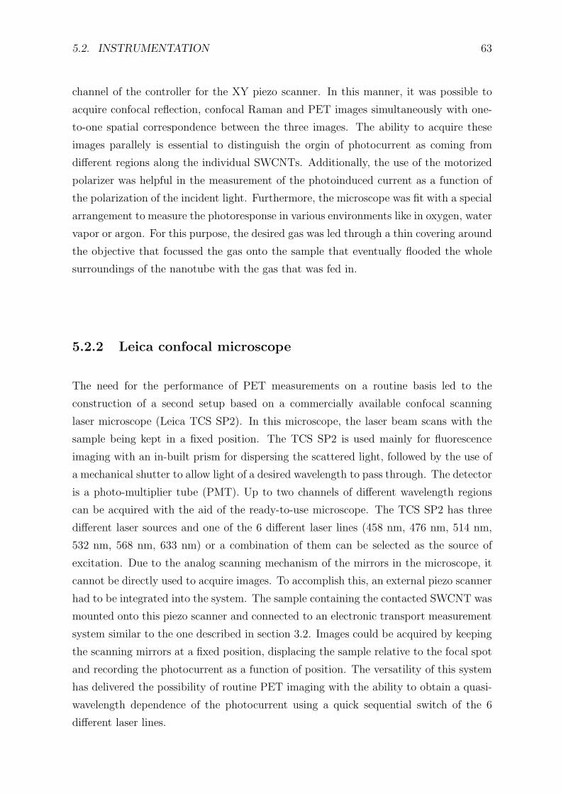
5.2. INSTRUMENTATION 63
channel of the controller for the XY piezo scanner. In this manner, it was possible to
acquire confocal reflection, confocal Raman and PET images simultaneously with one-
to-one spatial correspondence between the three images. The ability to acquire these
images parallely is essential to distinguish the orgin of photocurrent as coming from
different regions along the individual SWCNTs. Additionally, the use of the motorized
polarizer was helpful in the measurement of the photoinduced current as a function of
the polarization of the incident light. Furthermore, the microscope was fit with a special
arrangement to measure the photoresponse in various environments like in oxygen, water
vapor or argon. For this purpose, the desired gas was led through a thin covering around
the objective that focussed the gas onto the sample that eventually flooded the whole
surroundings of the nanotube with the gas that was fed in.
5.2.2 Leica confocal microscope
The need for the performance of PET measurements on a routine basis led to the
construction of a second setup based on a commercially available confocal scanning
laser microscope (Leica TCS SP2). In this microscope, the laser beam scans with the
sample being kept in a fixed position. The TCS SP2 is used mainly for fluorescence
imaging with an in-built prism for dispersing the scattered light, followed by the use of
a mechanical shutter to allow light of a desired wavelength to pass through. The detector
is a photo-multiplier tube (PMT). Up to two channels of different wavelength regions
can be acquired with the aid of the ready-to-use microscope. The TCS SP2 has three
different laser sources and one of the 6 different laser lines (458 nm, 476 nm, 514 nm,
532 nm, 568 nm, 633 nm) or a combination of them can be selected as the source of
excitation. Due to the analog scanning mechanism of the mirrors in the microscope, it
cannot be directly used to acquire images. To accomplish this, an external piezo scanner
had to be integrated into the system. The sample containing the contacted SWCNT was
mounted onto this piezo scanner and connected to an electronic transport measurement
system similar to the one described in section 3.2. Images could be acquired by keeping
the scanning mirrors at a fixed position, displacing the sample relative to the focal spot
and recording the photocurrent as a function of position. The versatility of this system
has delivered the possibility of routine PET imaging with the ability to obtain a quasi-
wavelength dependence of the photocurrent using a quick sequential switch of the 6
different laser lines.
64 CHAPTER 5. PHOTOELECTRONIC TRANSPORT
5.3 Photoelectronic transport in semiconducting
SWCNTs
The electronic transport through s-SWCNTs under photo-illumination has been found
to be strongly influenced by the type of metal that is used to contact them. When using
pure AuPd, the contact is more ohmic and the band alignment between the SWCNT
and the metal leads is roughly mid-gap. The use of Ti as an adhesion layer on top
of the SWCNTs produces a pronounced Schottky barrier at the contact, but imparts
a smaller sensitivity to the surroundings. By contrast, the thickness of the thermally
grown SiO2 layer that serves as the gate insulator has only a negligible effect on the pho-
toelectronic transport through individual SWCNTs. In the following, the observation
of photoconductivity in individual SWCNTs using a focussed beam of visible laser light
is presented. Then, the use of PET imaging to identify the local origin of photoconduc-
tivity and the effect of Schottky barriers at the contacts is described. The observations
reported here concern only the devices containing arc-dicharge SWCNTs contacted by
AuPd/Ti electrodes.
5.3.1 Photoconductivity in s-SWCNTs
Individual s-SWCNTs were identified with the help of AFM height images and their
strong gate dependence of conductance. In total, 12 different s-SWCNT devices were
investigated in this work and all of them exhibited p-type behavior with a GDR exceed-
ing 103 in a VG range of ±5 V. A representative example of such a device is depicted in
Fig. 5.2. Fig. 5.2(a) shows an AFM amplitude image with a single s-SWCNT contacted
between the two electrodes. The GDC curve for this device is shown in Fig. 5.2(b), which
displays a GDR of ≈ 104 and a pronounced hysteresis. A confocal Raman image of the
G-line intensity, acquired using the green line (λexc = 514.5 nm, 0.5 MW/cm2) overlaid
above a simultaneously acquired reflection image is shown in Fig. 5.2(c). The combina-
tion of the reflection image and the Raman image helps in identifying the exact location
of the contacted s-SWCNT, which subsequently enables positioning of the incident laser
spot exactly above the specific SWCNT bridging the electrode gap. A Raman spectrum
of this s-SWCNT could then be obtained, which is displayed in Fig. 5.2(d). The Raman
spectrum ensures additionally that this tube is semiconducting, as is apparent from the
absence of the BWF line characteristic of m-SWCNTs.
Before performing the PET experiments, the devices were switched to the OFF state
by performing one full gate voltage cycle. Specifically, the gate voltage is scanned to
5.3. PHOTOELECTRONIC TRANSPORT IN SEMICONDUCTING SWCNTS 65
Figure 5.2: Locating an individual s-SWCNT for PET measurements: (a) AFM amplitudeimage of a device comprising a single s-SWCNT (height ≈ 1.3±0.3 nm). (b) Gate dependenceof conductance for the same sample with Vds = 0.1 V. The arrows indicate the direction inwhich VG is scanned. (c) False color Raman G-line image of the sample (λexc = 514.5 nm,0.5 MW/cm2), overlaid with a reflection image to obtain the position of electrodes. (d) Ramanspectrum of the s-SWCNT taken with the laser spot positioned at the marked region (circle)of (c).
negative voltages and brought back to zero. Due to the hysteresis present in the device,
after the performance of this scan, the device remained in the OFF state long enough
to perform the subsequent measurements. Using the technique outlined in Fig. 5.2,
the laser spot was positioned over the tube approximately in the middle of the gap.
By using a manual shutter in the laser beam path, the effect of photo-illumination on
the current through the tube could be monitored for short laser pulses of intensities
varying in the range of 0.5 to 7.5 MW/cm2. A result of such a measurement is shown in
Fig. 5.3(a). It can be observed that the photoresponse is instantaneous within the limits
of the measurement speed used. The measured photocurrents are plotted as a function
of the incident laser intensity in Fig. 5.3(b), exhibiting a quasi-linear power dependence
of the photogenerated current. The slope of the linear fit has been determined to be
0.2 nA/( MW/cm2) or equivalently 2nS/( MW/cm2), comparable to the photoresponse
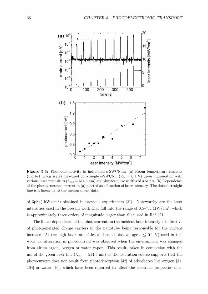
66 CHAPTER 5. PHOTOELECTRONIC TRANSPORT
Figure 5.3: Photoconductivity in individual s-SWCNTs: (a) Room temperature currents(plotted in log scale) measured on a single s-SWCNT (Vds = 0.1 V) upon illumination withvarious laser intensities (λexc = 514.5 nm) and shutter pulse widths of 3 or 7 s. (b) Dependenceof the photogenerated current in (a) plotted as a function of laser intensity. The dotted straightline is a linear fit to the measurement data.
of 3pS/( kW/cm2) obtained in previous experiments [21]. Noteworthy are the laser
intensities used in the present work that fall into the range of 0.5–7.5 MW/cm2, which
is approximately three orders of magnitude larger than that used in Ref. [21].
The linear dependence of the photocurrent on the incident laser intensity is indicative
of photogenerated charge carriers in the nanotube being responsible for the current
increase. At the high laser intensities and small bias voltages (≤ 0.1 V) used in this
work, no alteration in photocurrent was observed when the environment was changed
from air to argon, oxygen or water vapor. This result, taken in connection with the
use of the green laser line (λexc = 514.5 nm) as the excitation source supports that the
photocurrent does not result from photodesorption [42] of adsorbates like oxygen [31,
104] or water [76], which have been reported to affect the electrical properties of s-
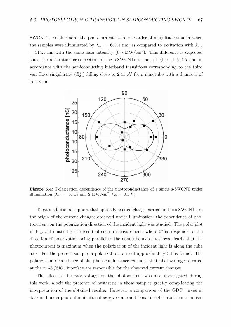
5.3. PHOTOELECTRONIC TRANSPORT IN SEMICONDUCTING SWCNTS 67
SWCNTs. Furthermore, the photocurrents were one order of magnitude smaller when
the samples were illuminated by λexc = 647.1 nm, as compared to excitation with λexc
= 514.5 nm with the same laser intensity (0.5 MW/cm2). This difference is expected
since the absorption cross-section of the s-SWCNTs is much higher at 514.5 nm, in
accordance with the semiconducting interband transitions corresponding to the third
van Hove singularties (Es33) falling close to 2.41 eV for a nanotube with a diameter of
≈ 1.3 nm.
Figure 5.4: Polarization dependence of the photoconductance of a single s-SWCNT underillumination (λexc = 514.5 nm, 2 MW/cm2, Vds = 0.1 V).
To gain additional support that optically excited charge carriers in the s-SWCNT are
the origin of the current changes observed under illumination, the dependence of pho-
tocurrent on the polarization direction of the incident light was studied. The polar plot
in Fig. 5.4 illustrates the result of such a measurement, where 0 corresponds to the
direction of polarization being parallel to the nanotube axis. It shows clearly that the
photocurrent is maximum when the polarization of the incident light is along the tube
axis. For the present sample, a polarization ratio of approximately 5:1 is found. The
polarization dependence of the photoconductance excludes that photovoltages created
at the n+-Si/SiO2 interface are responsible for the observed current changes.
The effect of the gate voltage on the photocurrent was also investigated during
this work, albeit the presence of hysteresis in these samples greatly complicating the
interpretation of the obtained results. However, a comparison of the GDC curves in
dark and under photo-illumination does give some additional insight into the mechanism
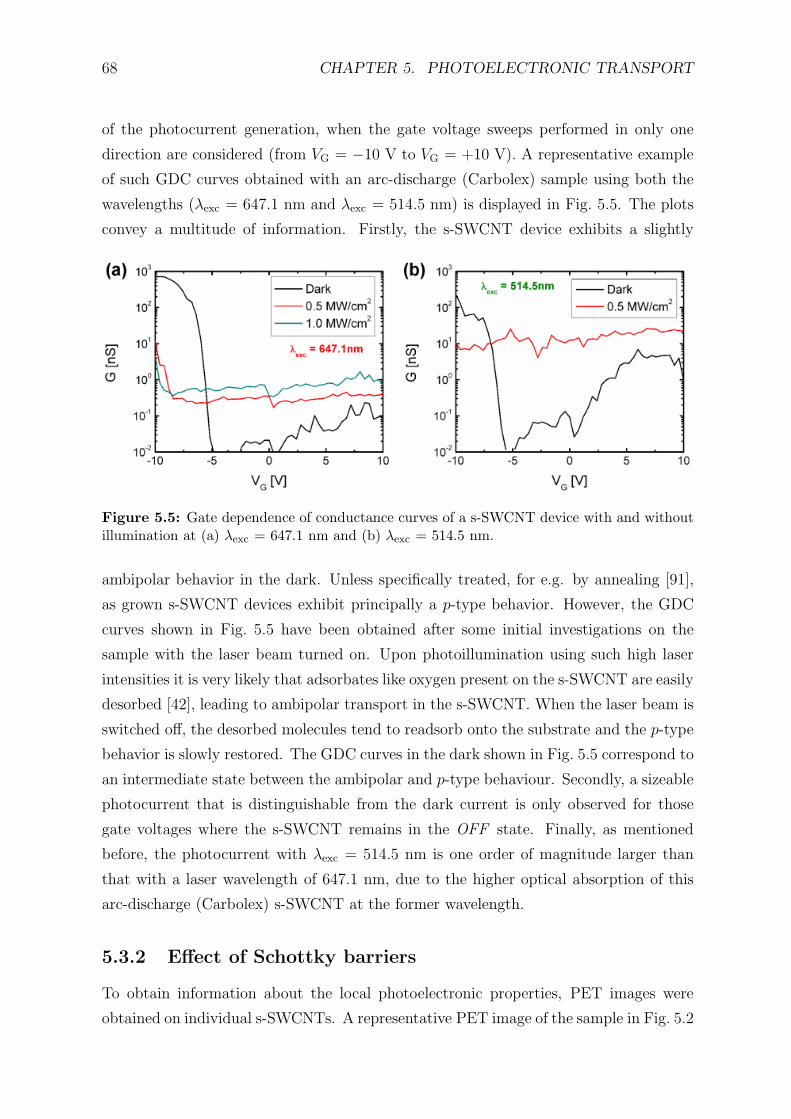
68 CHAPTER 5. PHOTOELECTRONIC TRANSPORT
of the photocurrent generation, when the gate voltage sweeps performed in only one
direction are considered (from VG = −10 V to VG = +10 V). A representative example
of such GDC curves obtained with an arc-discharge (Carbolex) sample using both the
wavelengths (λexc = 647.1 nm and λexc = 514.5 nm) is displayed in Fig. 5.5. The plots
convey a multitude of information. Firstly, the s-SWCNT device exhibits a slightly
Figure 5.5: Gate dependence of conductance curves of a s-SWCNT device with and withoutillumination at (a) λexc = 647.1 nm and (b) λexc = 514.5 nm.
ambipolar behavior in the dark. Unless specifically treated, for e.g. by annealing [91],
as grown s-SWCNT devices exhibit principally a p-type behavior. However, the GDC
curves shown in Fig. 5.5 have been obtained after some initial investigations on the
sample with the laser beam turned on. Upon photoillumination using such high laser
intensities it is very likely that adsorbates like oxygen present on the s-SWCNT are easily
desorbed [42], leading to ambipolar transport in the s-SWCNT. When the laser beam is
switched off, the desorbed molecules tend to readsorb onto the substrate and the p-type
behavior is slowly restored. The GDC curves in the dark shown in Fig. 5.5 correspond to
an intermediate state between the ambipolar and p-type behaviour. Secondly, a sizeable
photocurrent that is distinguishable from the dark current is only observed for those
gate voltages where the s-SWCNT remains in the OFF state. Finally, as mentioned
before, the photocurrent with λexc = 514.5 nm is one order of magnitude larger than
that with a laser wavelength of 647.1 nm, due to the higher optical absorption of this
arc-discharge (Carbolex) s-SWCNT at the former wavelength.
5.3.2 Effect of Schottky barriers
To obtain information about the local photoelectronic properties, PET images were
obtained on individual s-SWCNTs. A representative PET image of the sample in Fig. 5.2
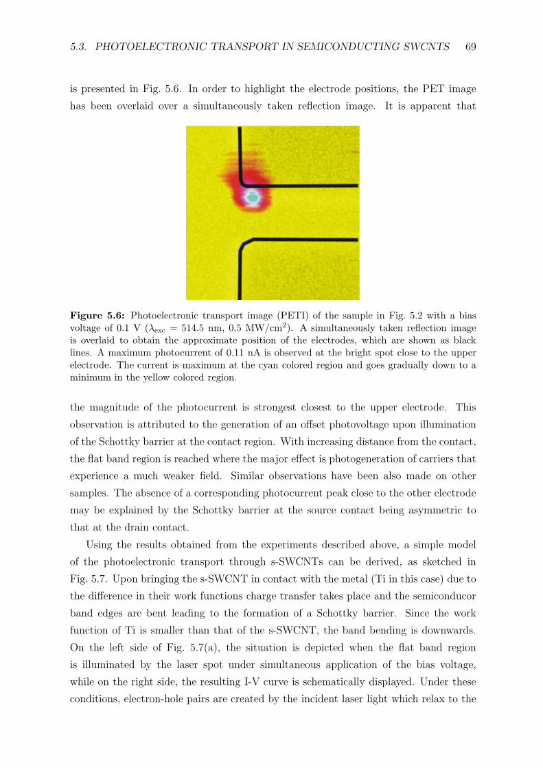
5.3. PHOTOELECTRONIC TRANSPORT IN SEMICONDUCTING SWCNTS 69
is presented in Fig. 5.6. In order to highlight the electrode positions, the PET image
has been overlaid over a simultaneously taken reflection image. It is apparent that
Figure 5.6: Photoelectronic transport image (PETI) of the sample in Fig. 5.2 with a biasvoltage of 0.1 V (λexc = 514.5 nm, 0.5 MW/cm2). A simultaneously taken reflection imageis overlaid to obtain the approximate position of the electrodes, which are shown as blacklines. A maximum photocurrent of 0.11 nA is observed at the bright spot close to the upperelectrode. The current is maximum at the cyan colored region and goes gradually down to aminimum in the yellow colored region.
the magnitude of the photocurrent is strongest closest to the upper electrode. This
observation is attributed to the generation of an offset photovoltage upon illumination
of the Schottky barrier at the contact region. With increasing distance from the contact,
the flat band region is reached where the major effect is photogeneration of carriers that
experience a much weaker field. Similar observations have been also made on other
samples. The absence of a corresponding photocurrent peak close to the other electrode
may be explained by the Schottky barrier at the source contact being asymmetric to
that at the drain contact.
Using the results obtained from the experiments described above, a simple model
of the photoelectronic transport through s-SWCNTs can be derived, as sketched in
Fig. 5.7. Upon bringing the s-SWCNT in contact with the metal (Ti in this case) due to
the difference in their work functions charge transfer takes place and the semiconducor
band edges are bent leading to the formation of a Schottky barrier. Since the work
function of Ti is smaller than that of the s-SWCNT, the band bending is downwards.
On the left side of Fig. 5.7(a), the situation is depicted when the flat band region
is illuminated by the laser spot under simultaneous application of the bias voltage,
while on the right side, the resulting I-V curve is schematically displayed. Under these
conditions, electron-hole pairs are created by the incident laser light which relax to the
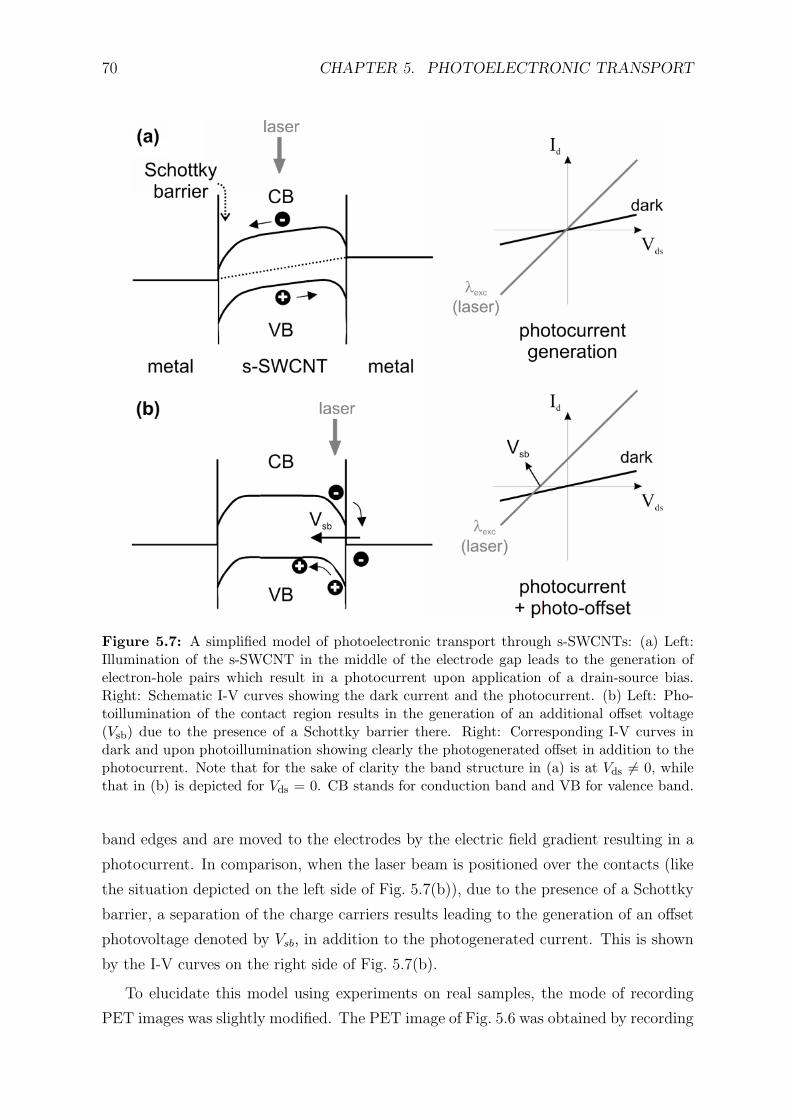
70 CHAPTER 5. PHOTOELECTRONIC TRANSPORT
Figure 5.7: A simplified model of photoelectronic transport through s-SWCNTs: (a) Left:Illumination of the s-SWCNT in the middle of the electrode gap leads to the generation ofelectron-hole pairs which result in a photocurrent upon application of a drain-source bias.Right: Schematic I-V curves showing the dark current and the photocurrent. (b) Left: Pho-toillumination of the contact region results in the generation of an additional offset voltage(Vsb) due to the presence of a Schottky barrier there. Right: Corresponding I-V curves indark and upon photoillumination showing clearly the photogenerated offset in addition to thephotocurrent. Note that for the sake of clarity the band structure in (a) is at Vds 6= 0, whilethat in (b) is depicted for Vds = 0. CB stands for conduction band and VB for valence band.
band edges and are moved to the electrodes by the electric field gradient resulting in a
photocurrent. In comparison, when the laser beam is positioned over the contacts (like
the situation depicted on the left side of Fig. 5.7(b)), due to the presence of a Schottky
barrier, a separation of the charge carriers results leading to the generation of an offset
photovoltage denoted by Vsb, in addition to the photogenerated current. This is shown
by the I-V curves on the right side of Fig. 5.7(b).
To elucidate this model using experiments on real samples, the mode of recording
PET images was slightly modified. The PET image of Fig. 5.6 was obtained by recording
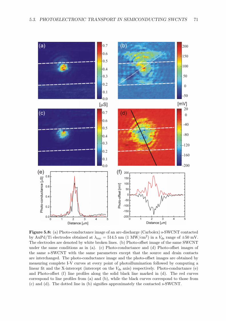
5.3. PHOTOELECTRONIC TRANSPORT IN SEMICONDUCTING SWCNTS 71
Figure 5.8: (a) Photo-conductance image of an arc-discharge (Carbolex) s-SWCNT contactedby AuPd/Ti electrodes obtained at λexc = 514.5 nm (1 MW/cm2) in a Vds range of ±50 mV.The electrodes are denoted by white broken lines. (b) Photo-offset image of the same SWCNTunder the same conditions as in (a). (c) Photo-conductance and (d) Photo-offset images ofthe same s-SWCNT with the same parameters except that the source and drain contactsare interchanged. The photo-conductance image and the photo-offset images are obtained bymeasuring complete I-V curves at every point of photoillumination followed by computing alinear fit and the X-intercept (intercept on the Vds axis) respectively. Photo-conductance (e)and Photo-offset (f) line profiles along the solid black line marked in (d). The red curvescorrespond to line profiles from (a) and (b), while the black curves correspond to those from(c) and (d). The dotted line in (b) signifies approximately the contacted s-SWCNT.
72 CHAPTER 5. PHOTOELECTRONIC TRANSPORT
the current Id as a function of the position of the laser spot at a fixed drain-source bias
of 0.1 V. Under these circumstances, the lobe seen in the PET image close to the top
electrode contains the contribution of both the photocurrent and the photo-offset. In
the present experiments, using the Leica microscope the acquisition of PET images
was made in such a way that complete I-V curves could be measured at every point
during the scan of the sample below the laser spot. As a consequence of this, the
linear fit of the I-V curves (corresponding to resistance or conductance) and the X-
intercept (intercept on the Vds axis) of I-V curves (corresponding to an offset voltage)
could be calculated at every point. This resulted in two PET images – one of them
a photo-resistance or photo-conductance image and the other a photo-offset voltage
image. The result of such a measurement is summarized in Fig. 5.8. Figs. 5.8(a) and
(b) show respectively the photo-conductance (log scale) and the photo-offset images of
the sample taken using the resonant laser wavelength of 514.5 nm. Figs. 5.8(c) and
(d) are corresponding images obtained by exchanging source and drain under the same
conditions. The line profiles in the photo-conductance image of Fig. 5.8(e) show clearly
that close to one of the contacts, there is a increase in conductance by around one order
of magnitude upon photoillumination. This corresponds to the contribution purely due
to photoconductivity in this s-SWCNT. The line profiles along the photo-offset images
shown in Fig. 5.8(f) display an offset voltage in the same region close to the electrodes.
The change in sign of the photovoltage upon exchange of source and drain leads gives
additional support for the creation of a photo-offset voltage across the Schottky barrier.
The experimental results presented in Fig. 5.8 are in good agreement with the model
outlined in Fig. 5.7.
Although the model explains the creation of photo-offset voltages at the Schottky
barriers and the generation of photoconductivity, it does not directly explain the ob-
servation of a PETI lobe close to only one of the electrodes in all of the 12 tubes for
the contact configuration investigated here. This could be due to a variety of reasons.
The SWCNTs obtained from the arc-discharge process are normally coated with a sub-
stantial amount of amorphous carbon and are rather inhomogeneous, especially over
lengths more than 1 µm. One possibility could be the tube being composed of two dif-
ferent segments of different electrical character, for instance a s-SWCNT connected to a
m-SWCNT through a defect site. Another possibility is the creation of asymmetric con-
tacts to the same s-SWCNT as has also been observed in other experiments [107,108].
In such a configuration, the Schottky barrier on one of the contacts could obscure the
effect of the Schottky barrier at the other end, due to a large difference in the barrier
heights at the two contacts.
5.4. PHOTOELECTRONIC TRANSPORT IN METALLIC SWCNTS 73
5.4 Photoelectronic transport in metallic SWCNTs
m-SWCNTs represent attractive building blocks for ultra-small electronic devices, such
as nanoscale interconnects of high current carrying capability [109]. However, the suc-
cessful fabrication of such devices still requires a deeper understanding of the local
electronic properties of m-SWCNTs and their connection to leads. Various methods
have been demonstrated that utilize a probe with dimensions of a few tens of nm to ob-
tain molecular scale electronic structure information along electrically contacted tubes.
While resonant electron scattering at defect sites could be observed in m-SWCNTs by
varying the local Fermi level through the voltage applied to the AFM tip [86], conduct-
ing tip AFM (CT-AFM) proved useful to infer the presence of asymmetric electrical
contacts to the same individual SWCNT bundle [107]. In addition, potential variations
along a m-SWCNT could be imaged through an electrostatic AFM (EFM) indicating
clearly that the voltage drop along the tube occurs precisely at an intrinsic or inten-
tionally introduced defect site [110, 111]. Thus the contacts of the m-SWCNTs to the
leads and structural inhomogeneities along them seem to have a strong effect on the
electronic transport. In this work, photo-excitation has been used as a probe to gather
electronic structure information at a local scale along individual m-SWCNTs. Unlike
s-SWCNTs the photoelectronic transport through m-SWCNTs was found to be rather
independent of whether AuPd or AuPd/Ti was used as the metal contact. The samples
were fabricated using either arc-discharge (Carbolex) or HiPco tubes contacted by elec-
trodes in the 1.3 µm gap architecture. The experiments were performed on a total of
15 m-SWCNTs by obtaining PET images. The images were acquired by recording the
drain current (Id) at zero drain-source bias (Vds = 0 V), unless otherwise mentioned.
5.4.1 Schottky barriers in m-SWCNT devices
For the results presented here, m-SWCNTs with almost no variation of gate dependence
of conductance were used. These samples displayed a GDR less than two (referred to as
type I) Fig. 5.9(a) displays the AFM image of a representative sample (HiPco) of type I,
comprising an apparently homogeneous nanotube with no discernible structural defect.
At high drain-source bias, the dark current through the tube was found to saturate
at 25 µA, in accordance with previous observations on individual m-SWCNTs of high
structural integrity [112]. Fig. 5.9(b) displays the PET image obtained at zero-bias for
this sample. Two oppositely signed lobes can be clearly identified at the contacts, as
can also be inferred from the line profiles of the PET image shown in Fig. 5.9(c). To
gain more insight into the origin of the two lobes, the source and drain electrodes were
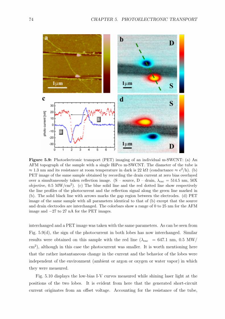
74 CHAPTER 5. PHOTOELECTRONIC TRANSPORT
Figure 5.9: Photoelectronic transport (PET) imaging of an individual m-SWCNT: (a) AnAFM topograph of the sample with a single HiPco m-SWCNT. The diameter of the tube is≈ 1.3 nm and its resistance at room temperature in dark is 22 kΩ (conductance ≈ e2/h). (b)PET image of the same sample obtained by recording the drain current at zero bias overlayedover a simultaneously taken reflection image. (S – source, D – drain, λexc = 514.5 nm, 50Xobjective, 0.5 MW/cm2). (c) The blue solid line and the red dotted line show respectivelythe line profiles of the photocurrent and the reflection signal along the green line marked in(b). The solid black line with arrows marks the gap region between the electrodes. (d) PETimage of the same sample with all parameters identical to that of (b) except that the sourceand drain electrodes are interchanged. The colorbars show a range of 0 to 25 nm for the AFMimage and −27 to 27 nA for the PET images.
interchanged and a PET image was taken with the same parameters. As can be seen from
Fig. 5.9(d), the sign of the photocurrent in both lobes has now interchanged. Similar
results were obtained on this sample with the red line (λexc = 647.1 nm, 0.5 MW/
cm2), although in this case the photocurrent was smaller. It is worth mentioning here
that the rather instantaneous change in the current and the behavior of the lobes were
independent of the environment (ambient or argon or oxygen or water vapor) in which
they were measured.
Fig. 5.10 displays the low-bias I-V curves measured while shining laser light at the
positions of the two lobes. It is evident from here that the generated short-circuit
current originates from an offset voltage. Accounting for the resistance of the tube,
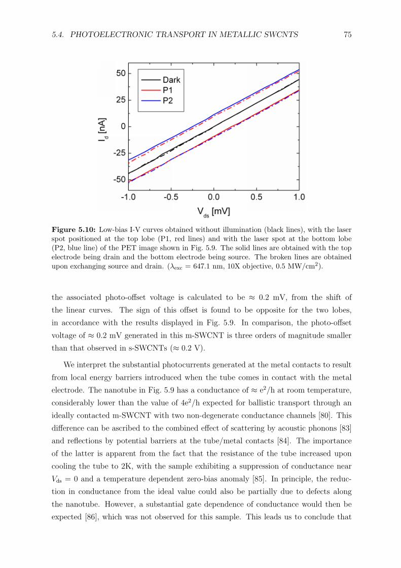
5.4. PHOTOELECTRONIC TRANSPORT IN METALLIC SWCNTS 75
Figure 5.10: Low-bias I-V curves obtained without illumination (black lines), with the laserspot positioned at the top lobe (P1, red lines) and with the laser spot at the bottom lobe(P2, blue line) of the PET image shown in Fig. 5.9. The solid lines are obtained with the topelectrode being drain and the bottom electrode being source. The broken lines are obtainedupon exchanging source and drain. (λexc = 647.1 nm, 10X objective, 0.5 MW/cm2).
the associated photo-offset voltage is calculated to be ≈ 0.2 mV, from the shift of
the linear curves. The sign of this offset is found to be opposite for the two lobes,
in accordance with the results displayed in Fig. 5.9. In comparison, the photo-offset
voltage of ≈ 0.2 mV generated in this m-SWCNT is three orders of magnitude smaller
than that observed in s-SWCNTs (≈ 0.2 V).
We interpret the substantial photocurrents generated at the metal contacts to result
from local energy barriers introduced when the tube comes in contact with the metal
electrode. The nanotube in Fig. 5.9 has a conductance of ≈ e2/h at room temperature,
considerably lower than the value of 4e2/h expected for ballistic transport through an
ideally contacted m-SWCNT with two non-degenerate conductance channels [80]. This
difference can be ascribed to the combined effect of scattering by acoustic phonons [83]
and reflections by potential barriers at the tube/metal contacts [84]. The importance
of the latter is apparent from the fact that the resistance of the tube increased upon
cooling the tube to 2K, with the sample exhibiting a suppression of conductance near
Vds = 0 and a temperature dependent zero-bias anomaly [85]. In principle, the reduc-
tion in conductance from the ideal value could also be partially due to defects along
the nanotube. However, a substantial gate dependence of conductance would then be
expected [86], which was not observed for this sample. This leads us to conclude that
76 CHAPTER 5. PHOTOELECTRONIC TRANSPORT
for the present nanotube, the barriers at the contacts restrict the charge transport. Al-
though metallic SWCNTs with nearly perfect contacts have been demonstrated using
pure palladium [77], nanotubes contacted with other metals generally exhibit signatures
of contact barriers [77,84,113]. This barrier formation can be ascribed to band bending
as a result of charge transfer due to the equilibration of Fermi levels when the nan-
otube and the metal electrode are brought in contact [114, 115]. Added to this, the
1D/3D-characteristic of this contact region [85], which differs from a simple 3D/3D-
metal interface results in the creation of built-in fields, and the contact region behaves
like a Schottky barrier. Based on these arguments, the photo-voltage generation at the
metallic nanotube/AuPd interface can be understood to originate from electron/hole-
pairs locally created by photo-excitation, followed by the separation of electrons and
holes due to the local built-in electric field. In this process, the interband transition
between the first van Hove singularities in the m-SWCNT (Em11) provides the neces-
sary absorption cross-section. This is consistent with the observation that the metallic
HiPCO tubes showed larger photocurrent signals when illuminated at 514.5 nm than at
647.1 nm under otherwise identical conditions, in accordance with previous reports of
stronger optical absorption for the HiPCO tubes at 514.5 nm [116,117].
When the nanotube is brought in contact with the metal electrode, the internal
electric field generated due to charge transfer is directed towards the metal electrode.
Seen from the source lead, the electric field at the source contact is oriented opposite
to that of the electric field at the drain contact. As a consequence of this, the gener-
ated photocurrents are in opposing directions at the two contacts, which explains the
opposite signs of the two lobes in the PET image (Fig. 5.9(b)). In all of the measured
samples, the photocurrent is negative at the drain electrode (the electron flow is from
source to drain), which indicates that the nanotube electronic bands experience an up-
ward bending at the contacts, in agreement with the fact that the work function of
the nanotube is smaller than that of AuPd [115]. The identical magnitude of the pho-
tocurrents generated at the two contacts of the sample in figure 1 implies the presence
of symmetric contact barriers. Some samples, however, displayed considerably differ-
ent magnitudes of the peak photocurrent at the two electrodes. This finding indicates
the formation of asymmetric contacts, similar to observations made on semiconducting
nanotubes [107, 108]. With respect to the spatial extent of the barrier region, the fact
that the lobes appear slightly elongated only in the scanning direction, but not in the
direction along the tube axis, suggests a value of the order of a few nm for the depletion
length, far below the resolution of the confocal microscope (≈ 250 nm) [118,119].
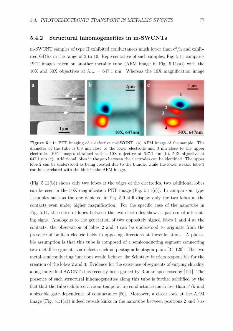
5.4. PHOTOELECTRONIC TRANSPORT IN METALLIC SWCNTS 77
5.4.2 Structural inhomogeneities in m-SWCNTs
m-SWCNT samples of type II exhibited conductances much lower than e2/h and exhib-
ited GDRs in the range of 3 to 10. Representative of such samples, Fig. 5.11 compares
PET images taken on another metallic tube (AFM image in Fig. 5.11(a)) with the
10X and 50X objectives at λexc = 647.1 nm. Whereas the 10X magnification image
Figure 5.11: PET imaging of a defective m-SWCNT: (a) AFM image of the sample. Thediameter of the tube is 0.9 nm close to the lower electrode and 3 nm close to the upperelectrode. PET images obtained with a 10X objective at 647.1 nm (b), 50X objective at647.1 nm (c). Additional lobes in the gap between the electrodes can be identified. The upperlobe 2 can be understood as being created due to the bundle, while the lower weaker lobe 3can be correlated with the kink in the AFM image.
(Fig. 5.11(b)) shows only two lobes at the edges of the electrodes, two additional lobes
can be seen in the 50X magnification PET image (Fig. 5.11(c)). In comparison, type
I samples such as the one depicted in Fig. 5.9 still display only the two lobes at the
contacts even under higher magnification. For the specific case of the nanotube in
Fig. 5.11, the series of lobes between the two electrodes shows a pattern of alternat-
ing signs. Analogous to the generation of two oppositely signed lobes 1 and 4 at the
contacts, the observation of lobes 2 and 3 can be understood to originate from the
presence of built-in electric fields in opposing directions at these locations. A plausi-
ble assumption is that this tube is composed of a semiconducting segment connecting
two metallic segments via defects such as pentagon-heptagon pairs [31, 120]. The two
metal-semiconducting junctions would behave like Schottky barriers responsible for the
creation of the lobes 2 and 3. Evidence for the existence of segments of varying chirality
along individual SWCNTs has recently been gained by Raman spectroscopy [121]. The
presence of such structural inhomogeneities along this tube is further solidified by the
fact that the tube exhibited a room-temperature conductance much less than e2/h and
a sizeable gate dependence of conductance [86]. Moreover, a closer look at the AFM
image (Fig. 5.11(a)) indeed reveals kinks in the nanotube between positions 2 and 3 as
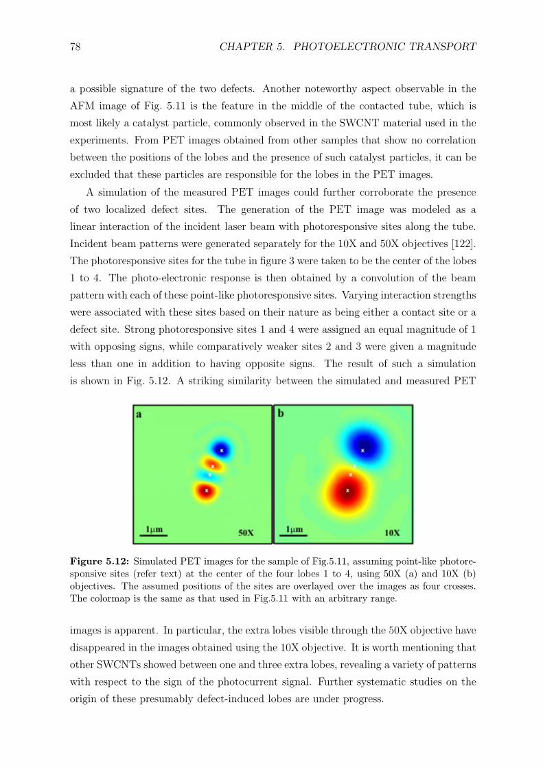
78 CHAPTER 5. PHOTOELECTRONIC TRANSPORT
a possible signature of the two defects. Another noteworthy aspect observable in the
AFM image of Fig. 5.11 is the feature in the middle of the contacted tube, which is
most likely a catalyst particle, commonly observed in the SWCNT material used in the
experiments. From PET images obtained from other samples that show no correlation
between the positions of the lobes and the presence of such catalyst particles, it can be
excluded that these particles are responsible for the lobes in the PET images.
A simulation of the measured PET images could further corroborate the presence
of two localized defect sites. The generation of the PET image was modeled as a
linear interaction of the incident laser beam with photoresponsive sites along the tube.
Incident beam patterns were generated separately for the 10X and 50X objectives [122].
The photoresponsive sites for the tube in figure 3 were taken to be the center of the lobes
1 to 4. The photo-electronic response is then obtained by a convolution of the beam
pattern with each of these point-like photoresponsive sites. Varying interaction strengths
were associated with these sites based on their nature as being either a contact site or a
defect site. Strong photoresponsive sites 1 and 4 were assigned an equal magnitude of 1
with opposing signs, while comparatively weaker sites 2 and 3 were given a magnitude
less than one in addition to having opposite signs. The result of such a simulation
is shown in Fig. 5.12. A striking similarity between the simulated and measured PET
Figure 5.12: Simulated PET images for the sample of Fig.5.11, assuming point-like photore-sponsive sites (refer text) at the center of the four lobes 1 to 4, using 50X (a) and 10X (b)objectives. The assumed positions of the sites are overlayed over the images as four crosses.The colormap is the same as that used in Fig.5.11 with an arbitrary range.
images is apparent. In particular, the extra lobes visible through the 50X objective have
disappeared in the images obtained using the 10X objective. It is worth mentioning that
other SWCNTs showed between one and three extra lobes, revealing a variety of patterns
with respect to the sign of the photocurrent signal. Further systematic studies on the
origin of these presumably defect-induced lobes are under progress.
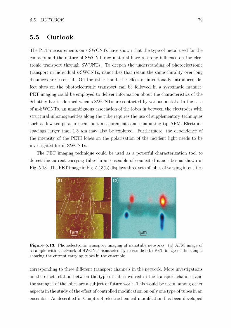
5.5. OUTLOOK 79
5.5 Outlook
The PET measurements on s-SWCNTs have shown that the type of metal used for the
contacts and the nature of SWCNT raw material have a strong influence on the elec-
tronic transport through SWCNTs. To deepen the understanding of photoelectronic
transport in individual s-SWCNTs, nanotubes that retain the same chirality over long
distances are essential. On the other hand, the effect of intentionally introduced de-
fect sites on the photoelectronic transport can be followed in a systematic manner.
PET imaging could be employed to deliver information about the characteristics of the
Schottky barrier formed when s-SWCNTs are contacted by various metals. In the case
of m-SWCNTs, an unambiguous association of the lobes in between the electrodes with
structural inhomogeneities along the tube requires the use of supplementary techniques
such as low-temperature transport measurements and conducting tip AFM. Electrode
spacings larger than 1.3 µm may also be explored. Furthermore, the dependence of
the intensity of the PETI lobes on the polarization of the incident light needs to be
investigated for m-SWCNTs.
The PET imaging technique could be used as a powerful characterization tool to
detect the current carrying tubes in an ensemble of connected nanotubes as shown in
Fig. 5.13. The PET image in Fig. 5.13(b) displays three sets of lobes of varying intensities
Figure 5.13: Photoelectronic transport imaging of nanotube networks: (a) AFM image ofa sample with a network of SWCNTs contacted by electrodes (b) PET image of the sampleshowing the current carrying tubes in the ensemble.
corresponding to three different transport channels in the network. More investigations
on the exact relation between the type of tube involved in the transport channels and
the strength of the lobes are a subject of future work. This would be useful among other
aspects in the study of the effect of controlled modification on only one type of tubes in an
ensemble. As described in Chapter 4, electrochemical modification has been developed

80 CHAPTER 5. PHOTOELECTRONIC TRANSPORT
into a versatile tool for the attachment of desired functional groups onto individual
SWCNTs in a covalent or non-covalent manner. The effect of such a modification on the
electronic transport could be studied at a local scale with photoillumination as the probe.
Obtaining PET images on such modified samples can be expected to deliver useful
information about the electronic structure of the modified nanotubes. Moreover, the use
of the confocal laser microscope in combination with electronic transport measurements
opens up the possibility to perform local photochemistry and photoelectrochemistry
on individual SWCNTs, by simultaneously monitoring in situ the electronic transport
through them. Taken together, the understanding gained from these experiments will
have important implications for the fabrication of future optoelectronic and photovoltaic
devices.
Chapter 6
Summary and Conclusion
In this thesis, electrochemical modification (ECM) and photoelectronic transport prop-
erties of individual SWCNTs have been presented. While the former has enabled the
demonstration of a generic route towards fabrication of field-effect transistors, the latter
has delivered important results that strengthen the understanding of electronic transport
through individual SWCNTs.
ECM of individual nanotubes has been studied using two different coupling schemes.
One method was based on the reduction of a highly reactive diazonium salt leading to
covalently attached phenyl groups around the SWCNTs. The second scheme utilized
the oxidation of a substituted aromatic amine providing a non-covalent coating onto
the SWCNTs. The respective covalent and non-covalent characters of the two coupling
schemes have been concluded from a combined electronic transport and confocal Raman
spectroscopic study of the coated SWCNTs. This study was performed separately with
m-SWCNTs and s-SWCNTs. The diazonium coupling to both the types of SWCNTs
resulted in an increase of both the resistance and the relative Raman D-line intensity
after ECM, which signifies the formation of chemical bonds between the polymer layer
and the carbon framework of the nanotube. By contrast, only minor changes in the con-
focal Raman spectra were detected after oxidative amine coupling on both m-SWCNTs
and s-SWCNTs. For this type of coupling, the electrical resistance of the m-SWCNTs
remained unchanged, whereas that of s-SWCNTs showed a moderate increase in resis-
tance. This increase in resistance can be understood by the decreased p-doping level of
the s-SWCNTs as a result of the electrons accepted during oxidation of the amine. Both
the coupling methods can be used to chemically tailor the surface properties of SWC-
NTs. While the covalent modification enables the alteration of the electronic properties
of the SWCNTs persistently, the SWCNTs modified by the oxidative scheme remain
mostly unaltered in their electronic structure.
81
82 CHAPTER 6. SUMMARY AND CONCLUSION
Incorporating the covalent ECM scheme, a generic fabrication route for SWCNT-
FETs, which combines electrochemistry and gate-induced modulation of conductivity
was demonstrated. It could be shown that the modification of s-SWCNTs can be en-
abled or blocked by varying the history of the gate potential scans before performing
electrochemistry. In this manner, the m-SWCNTs could be exclusively modified and
the conduction through only this kind of tubes in a SWCNT ensemble selectively elim-
inated, resulting in high–performance FETs. The FETs thus obtained displayed room-
temperature transconductances of ≈ 10 S/cm, switching ratios of up to 106 and hole
mobilities of ≈ 1000 cm2/Vs.
The results presented in this thesis are of importance for both fundamental studies
and applications. The study of electrochemical modification of SWCNTs at a single–tube
level is the first of its kind and represents an important step towards the understanding
of the mechanism of chemical attachment of molecular species onto the nanotubes. The
use of ECM towards applications was demonstrated by the fabrication of FETs through
selective ECM. Chemical and biological sensors with nanotubes coated to detect specific
functionalities seem viable using this method.
The photoelectronic transport properties of individual nanotubes were studied using
a confocal scanning optical microscope integrated with a setup for electronic transport
measurements. The photoexcitation of the carriers was achieved here by the use of
a laser spot that is diffraction-limited in size (with a diameter of approximately half
of the excitation wavelength). Individual s-SWCNTs were investigated by recording
photoconductivity and Raman spectra on the same electrically contacted s-SWCNTs.
It was observed that the magnitude of the photocurrent increased linearly with the laser
intensity. The photocurrent was found to be maximum for the light polarization being
parallel to the tube axis. The small extent of the laser spot generated by the confocal
microscope opened up the possibility to record photocurrent signals originating from
illumination at different locations along a contacted SWCNT, giving a photoelectronic
transport (PET) image. Using such PET images, significant photovoltage generation
close to the nanotube–electrode contact could be illustrated, which was attributed to
the presence of Schottky barriers there.
This imaging technique was then further applied to the study of the photoelectronic
properties of individual m-SWCNTs. The sizeable photocurrent signals observed at
the contacts were associated with the formation of depletion regions resulting from
the equilibration of the electrochemical potentials at the contact between m-SWCNTs
and metal electrodes. In addition, built–in electric fields at structural inhomogeneities
were found to effect a separation of photogenerated carriers leading to the creation

83
of a photooffset voltage at these regions. Taken together, it has been demonstrated
that spatially resolved photocurrent mapping represents an excellent tool to study the
local electronic structure of contact regions and to trace the presence of structural
inhomogeneities such as intermolecular junctions within nanotubes. The understanding
gained through the experimens performed in this thesis has strong implications for the
realisation of future optoelectornic and photonic devices.

84 CHAPTER 6. SUMMARY AND CONCLUSION

Bibliography
[1] Carbon Nanotubes – Science and Applications, (Ed.: M. Meyyappan), CRC
Press, Boca Raton, 2004.
[2] J. Aihara, J. Phys. Chem. 1994, 98, 9773.
[3] K. Balasubramanian, M. Burghard, Small 2005, 2, 180.
[4] W.P. Hoffman, W.C. Curley, T. Owens, H.T. Phan, J. Mater. Sci. 1991, 26,
4545.
[5] R.B. Mathur, J. Mittal, O.P. Bahl, N.K. Sandle, Carbon 1994, 32, 71.
[6] R. Saito, G. Dresselhaus, M.S. Dresselhaus Physical Properties of Carbon Nan-
otubes, (Imperial College Press: London), 1998.
[7] R. Martel, T. Shmidt, H.R. Shea, T. Hertel, Ph. Avouris, Appl. Phys. Lett. 1998,
73, 2447.
[8] S.J. Tans, A.R.M. Verschueren, C. Dekker, Nature 1998, 393, 49.
[9] Ph. Avouris, J. Appenzeller, R. Martel, S.J. Wind, Proc. IEEE 2003, 91, 1772.
[10] M.S. Fuhrer, B.M. Kim, T. Durkop, T. Brintlinger, Nano Lett. 2002, 2, 755.
[11] A. Javey, J. Guo, Q. Wang, M. Lundstrom, H. Dai, Nature 2003, 424, 654.
[12] D. Chattopadhyay, I. Galeska, F. Papadimitrakopoulos, J. Am. Chem. Soc.
2003, 125, 3370.
[13] Z. Chen, X. Du, M-H. Du, C.D. Rancken, H-P. Cheng, A.G. Rinzler, Nano Lett.
2003, 3, 1245.
[14] R. Krupke, F. Hennrich, H.v. Lohneysen, M.M. Kappes, Science 2003, 301,
344.
85
86 BIBLIOGRAPHY
[15] M. Zheng, M, A. Jagota, E.D. Semke, B.A. Diner, R.S. McLean, S.R. Lustig,
R.E: Richardson, N.G. Tassi, Nature Materials 2003, 2, 338.
[16] P.G. Collins, M.S. Arnold, Ph. Avouris, Science 2001, 292, 706.
[17] C.L. Kane, E.J. Mele, Phys. Rev. Lett. 2003, 90, 207401.
[18] A. Fujiware et al., Jpn. J. Appl. Phys. 2001, 40, L1229.
[19] Y. Kamada, N. Naka, N. Nagasawa, Z.M. Li, Z.K. Tang, Physica B 2002, 323,
239.
[20] Y. Zhang, S. Iijima, Phys. Rev. Lett. 1999, 82, 3472.
[21] M. Freitag, Y. Martin, J.A. Misewich, R. Martel, Ph. Avouris, Nano Lett. 2003,
3, 1067.
[22] H.W. Zhu, C.L. Xu, D.H. Wu, B.Q. Wei, R. Vajtai, P.M. Ajayan, Science 2002,
296, 884.
[23] S. Iijima, Nature 1991, 354, 56.
[24] S. Iijima, T. Ichihashi, Nature 1993, 363, 603.
[25] D.S. Bethune, C.H. Kiang, M.S. DeVries, G. Gorman, R. Savoy and R. Beyers,
Nature 1993, 363, 605.
[26] J.W. Mintmire, B.I. Dunlap, C.T. White, Phys. Rev. Lett. 1992, 68, 631.
[27] J.W. Mintmire, D.H. Robertson, C.T. White, J. Phys. Chem. Solids 1993, 54,
1835.
[28] R. Saito, M. Fujita, G. Dresselhaus, M.S. Dresselhaus, Phy. Rev. B 1992, 46,
1804.
[29] N.W. Ashcroft, N.D. Mermin Solid state physics, (Saunders College Publishing),
1976.
[30] R. Saito, G. Dresselhaus, M.S. Dresselhaus, Phys. Rev. B 2000, 61, 2981.
[31] Carbon Nanotubes: Synthesis, Structure Properties and Applications, (Ed.: M.S.
Dresselhaus, G. Dresselhaus, Ph. Avouris), Springer Verlag: Berlin, 2001.
[32] S. Frank, P. Poncharal, Y.L. Wang, W.A. deHeer, Science 1998, 280, 1744.
BIBLIOGRAPHY 87
[33] P. Petit, C. Mathis, C. Journet, P. Bernier, Chem. Phys. Lett. 1999, 305, 370. .
[34] M.J. O’Connell et al., Science 2002, 297, 593.
[35] M.S. Dresselhaus, P.C. Eklund, Adv. Phys. 2000, 49, 705.
[36] H. Kataura, et al., Synth. Met. 1999, 103, 2555.
[37] E.V. Basiuk, M. Monroy-Pelaez, I. Puente-Lee, V.A. Basiuk, Nano Lett. 2004,
4, 863.
[38] K. Mylvaganam, L.C. Zhang, J. Phys. Chem. B 2004, 108, 5217.
[39] Z.F. Chen, W. Thiel, A. Hirsch, Chem. Phys. Chem. 2003, 4, 93.
[40] H. Hu, P. Bhowmik, B. Zhao, M.A. Hamon, M.E. Itkis, R.C. Haddon, Chem.
Phys. Lett. 2001, 345, 25.
[41] J. Zhao, H. Park, J. Han, J.P. Lu, J. Phys. Chem. B 2004, 108, 4227.
[42] R.J. Chen, N.R. Franklin, J. Kong, J. Cao, T.W. Tombler, Y. Zhang, H. Dai,
Appl. Phys. Lett. 2001, 79, 2258.
[43] J. Zhang, H. Zou, Q. Qing, Y. Yang, Q. Li, Z. Liu, X. Guo, Z. Du, J. Phys.
Chem. B 2003, 107, 3712.
[44] E. Katz, I. Willner, Chem. Phys. Chem. 2004, 5, 1085.
[45] K.A.S. Fernando, Y. Lin, Y.P. Sun, Langmuir 2004, 20, 4777.
[46] M.A. Hamon, J. Chen, H. Hu, Y.S. Chen, M.E. Itkis, A.M. Rao, P.C. Eklund,
R.C. Haddon, Adv. Mater. 1999, 11, 834.
[47] J. Chen et al., J. Phys. Chem. B 2001, 105, 2525.
[48] J.L. Bahr, J.M. Tour, J. Mater. Chem. 2002, 12, 1952.
[49] A. Hirsch, Angew. Chem. Int. Ed. 2002, 41, 1853.
[50] C.A. Dyke, J.M. Tour, Chem. Eur. J. 2004, 10, 813.
[51] H.F. Bettinger, Chem. Phys. Chem. 2003, 4, 1283.
[52] V. Georgakilas, D. Voulgaris, E. Vzquez, M. Prato, D.M. Guldi, A. Kukovecz,
H. Kuzmany, J. Am. Chem. Soc. 2002, 124, 14318.
88 BIBLIOGRAPHY
[53] V.N. Khabashesku, W.E. Billups, J.L. Margrave, Acc. Chem. Res. 2002, 35,
1087.
[54] J.L. Stevens, A.Y. Huang, H.Q. Peng, L.W. Chiang, V.N. Khabashesku, J.L.
Margrave, Nano Lett. 2003, 3, 331.
[55] K. Balasubramanian et al., Adv. Mater. 2003, 15, 1515.
[56] J.L. Bahr, J. Yang, D.V. Kosynkin, M.J. Bronikowski, R.E. Smalley, J.M. Tour,
J. Am. Chem. Soc. 2001, 123, 6536.
[57] S. Kooi, U. Schlecht, M. Burghard, K. Kern, Angew. Chem. Int. Ed. 2002, 41,
1353.
[58] G.Z. Chen, M.S.P. Shaffer, D. Coleby, G. Dixon, W: Yhou, D.J. Fray, A:H.
Windle, Adv. Mater. 2000, 12, 522.
[59] M.J. Moghaddam, S. Taylor, M. Gao, S.M. Huang, L.M. Dai, M.J. McCall, Nano
Lett. 2004, 4, 89.
[60] J.B. Cui, M. Burghard, K. Kern, Nano Lett. 2003, 3, 613.
[61] S. Banerjee, S.S. Wong, J. Am. Chem. Soc. 2004, 126, 2073.
[62] T.W. Ebbesen, P.M. Ajayan, Nature 1992, 358, 220.
[63] C. Journet, P. Bernier, Appl. Phys. A 1998, 67, 1.
[64] http://www.carbolex.com
[65] http://www.mercorp.com
[66] M. Monthioux, B.W. Smith, B. Burteaux, A. Claye, J.E. Fischer, D.E. Luzzi,
Carbon 2001, 39, 1251.
[67] J. Kong, A.M. Cassell, H.J. Dai, Chem. Phys. Lett. 1998, 292, 567.
[68] Y. Murakami, Y. Miyauchi, S. Chiashi, S. Maruyama, Chem. Phys. Lett. 2003,
374, 53.
[69] Y. Li, W. Kim, Y. Zhang, M. Rolandi, D. Wang, H. Dai, J. Phys. Chem. B
2001, 105, 11424.
[70] J. Kong, C. Zhou, A. Morpurgo, H.T. Soh, C.F. Quate, C. Marcus, H.J. Dai,
Appl. Phys. A 1999, 69, 305.
BIBLIOGRAPHY 89
[71] M.J. Bronikowski, P.A. Willis, D.T. Colbert, K.A. Smith, R.E. Smalley, J. Vac.
Sci. Technol. A 2001, 19, 1800.
[72] Ph. Lambin, A. Loiseau, C. Culot, L.P. Biro, Carbon 2002, 40, 1635.
[73] M. Ouyang, J-L. Huang, C.M. Lieber, Annu. Rev. Phys. Chem. 2002, 53, 201.
[74] M. Radosavljevic, M. Freitag, K.V. Thadani, A.T. Johnson, Nano Lett. 2002,
2, 761.
[75] J.B. Cui, R. Sordan, M. Burghard, K. Kern, Appl. Phys. Lett. 2002, 81, 3260.
[76] W. Kim, A. Javey, O. Vermesh, Q. Wang, Y. Li, H. Dai, Nano Lett. 2003, 3,
193.
[77] D. Mann, A. Javey, J. Kong, Q. Wang, H. Dai, Nano Lett. 2003, 3, 1541.
[78] Y. Imry, R. Landauer, Rev. Mod. Phys. 1999, 71, S306.
[79] S. Datta Electronic transport in mesoscopic systems, (University Press: Cam-
bridge), 1995.
[80] W. Liang, M. Bockrath, D. Boyovic, J. Haffner, M. Tinkham, H. Park, Nature
2001, 411, 665.
[81] J. Kong, E. Yenilmez, T.W. Tombler, W. Kim, H. Dai, R. Laughlin, L. Liu, C.S.
Jayanthi, S.Y. Wu, Phys. Rev. Lett. 2001, 87, 106801.
[82] Y. Zhang, H. Dai, Appl. Phys. Lett. 2000, 77, 2015.
[83] S. Reich, C. Thomsen, J. Maultzsch Carbon Nanotubes: Basic Concepts and
Physical Properties, (Wiley-VCH: Weinheim), 2004.
[84] M. Bockrath, D.H. Cohen, P.L. McEuen, N.G. Chopra, A. Zettl, A. Thess, R.E.
Smalley, Science 1997, 275, 1922.
[85] Th. Hunger, B. Lengeler, J. Appenzeller, Phys. Rev. B 2004, 69, 195406.
[86] M. Bockrath, W. Liang, D. Bozovic, J.H. Hafner, C.M. Lieber, M. Tinkham, H.
Park, Science 2001, 291, 283.
[87] P.L. McEuen, M.S. Fuhrer, H. Park, IEEE Trans. Nanotech. 2002, 1, 78.
[88] S. Heinze, J. Tersoff, R. Martel, V. Derycke, J. Appenzeller, Ph. Avouris, Phys.
Rev. Lett. 2002, 89, 106801.

90 BIBLIOGRAPHY
[89] J. Appenzeller, J. Knoch, V. Derycke, R. Martel, S. Wind, Ph. Avouris, Phys.
Rev. Lett. 2002, 89, 126801.
[90] C. Zhou, J. Kong, H. Dai, Appl. Phys. Lett. 1999, 76, 1597.
[91] R. Martel, V. Derycke, C. Lavoie, J. Appenzeller, K.K. Chan, J. Tersoff, Ph.
Avouris, Phys. Rev. Lett. 2001, 87, 256805.
[92] A.M. Rao, E. Richter, S. Bandow, B. Chase, P.C. Eklund, K.A. Williams, Science
1997, 275, 187.
[93] Handbook of Microscopy, (Ed.: S. Amelinckx), xxx, 1997.
[94] F. Koberling Ph.D Dissertation: Fluoreszenzmikroskopische Untersuchungen an
einzelnen Halbleiter-Nanokristallen, (Verlag Dr. Hut: Munchen), 2001.
[95] C. Jiang et al., Phys. Rev. B 2002, 66, 161404.
[96] A.J. Downard, Electroanalysis 2000, 12, 1085.
[97] Y. Cui, Q. Wei, H. Park, C.M. Lieber, Science 2001, 293, 1289.
[98] Y.Chen et al., J. Mater. Res. 1998, 13, 2423.
[99] M.S. Strano et al., Science 2003, 301, 1519.
[100] S.J. Wind, J. Appenzeller, R. Martel, V. Derycke, Ph. Avouris, Appl. Phys. Lett.
2002, 80, 3817.
[101] S.M. Sze Physics of Semiconductor Devices, (Wiley: New York), 1981.
[102] J. Kong, N.R. Franklin, C. Zhou, M.G. Chapline, S. Peng, K. Cho, H. Dai,
Science 2000, 287, 622.
[103] I.A. Levitsky, W.B. Euler, Appl. Phys. Lett. 2003, 83, 1857.
[104] P.G. Collins, K. Bradley, M. Ishigami, A. Zettl, Science 2000, 287, 1801.
[105] S.H. Jhi, S.G. Louie, M.L. Cohen, Phys. Rev. Lett. 2000, 85, 1710.
[106] J. Zhao, J. Han, J.P. Lu, Phy. Rev. B 2002, 65, 193401.
[107] M. Freitag, M. Radosavljevic, W. Clauss, A.T. Johnson, Phys. Rev. B 2000,
62, R2307.
[108] K. Balasubramanian et al., Appl. Phys. Lett. 2004, 84, 2400.

BIBLIOGRAPHY 91
[109] H. Dai, E.W. Wong, C.M. Lieber, Science 1996, 272, 523.
[110] D. Bozovic, M. Bockrath, J.H. Hafner, C.M. Lieber, H. Park, M. Tinkham, Appl.
Phys. Lett. 2001, 78, 3693.
[111] A. Bachtold, M.S. Fuhrer, S. Plyasunov, M. Forero, E.H. Anderson, A. Zettl,
P.L. Mc Euen, Phys. Rev. Lett. 2000, 84, 6082.
[112] Z. Yao, C.L. Kane, C. Dekker, Phys. Rev. Lett. 2000, 84, 2941.
[113] A. Bezryadin, A.R.M. Verschueren, S.J. Tans, C. Dekker, Phys. Rev. Lett. 1998,
80, 4036.
[114] K. Kong, S. Han, J. Ihm, Phy. Rev. B 1999, 60, 6074.
[115] Y. Xue, M.A. Ratner, Phys. Rev. B 2004, 69, 161402.
[116] Y. Miyauchi, S. Chiashi, Y. Murakami, Y. Hayashida, S. Maruyma, Chem. Phys.
Lett. 2004, 387, 198.
[117] N. Zheng, X. Bu, B. Wang, P. Feng, Science 2002, 298, 2366.
[118] M. Freitag, M. Radosavljevic, Y. Yhou, A.T. Johnson, Appl. Phys. Lett. 2001,
79, 3326.
[119] F. Leonard, J. Tersoff, Phys. Rev. Lett. 1999, 83, 5174.
[120] A. Rochefort, Ph. Avouris, Nano Lett. 2002, 2, 253.
[121] C. Jiang, J. Zhao, H.A. Therese, M. Friedrich, A. Mews, J. Phys. Chem. B 2003,
107, 8742.
[122] R.W. Ditchburn Light, (Dover Publications: New York), 1961.

92 BIBLIOGRAPHY

Publications
Journal Articles
• K. Balasubramanian, M. Friedrich, C. Jiang, Y. Fan, A. Mews, M. Burghard and
K. Kern, Electrical transport and confocal Raman studies of electrochemically
modified individual carbon nanotubes, Adv. Mater. 2003, 15(18), 1515-1518.
• K. Balasubramanian, M. Friedrich, Y. Fan, U. Wannek, A. Mews, M. Burghard
and K. Kern, Photoelectronic transport imaging of individual semiconducting car-
bon nanotubes, Appl. Phys. Lett. 2004, 84(13), 2400-2402.
• K. Balasubramanian, R. Sordan, M. Burghard and K. Kern A selective electro-
chemical approach to carbon nanotube field-effect transistors, Nano Lett. 2004,
4(5), 827-830.
• K. Balasubramanian, M. Scolari, A. Mews, M. Burghard and K. Kern, Photocur-
rent imaging of charge transport barriers in carbon nanotube devices, Nano Lett.,
accepted.
Review Articles
• K. Balasubramanian, M. Burghard and K. Kern, Carbon Nanotubes: Electro-
chemical Modification, Dekker Encyclopedia of Nanoscience and Nanotechnology
2004, 507-517.
• K. Balasubramanian and M. Burghard, Funktionalisierte Kohlenstoff Nanorohren,
Chemie in unserer Zeit 2005, 39, 16-25.
• K. Balasubramanian and M. Burghard, Chemically functionalized carbon nan-
otubes, Small 2005, 2, 180-192.
93

94 PUBLICATIONS

Curriculum vitae
Name: Kannan Balasubramanian
Date of Birth: January 4, 1978
Nationality Republic of India
1994–1998 “Bachelor of Engineering” studies in Computer Science at
Birla Institute of Technology & Science, Pilani, India
1998–2000 “Scientist” at DaimlerChrysler Research Centre India, Ban-
galore, India
2000–2001 “Diplom der Ingenieurwissenschaften” in Elektrotechnik and
“Master of Science” in Electrical Communication Engineeer-
ing at the University of Kassel, Germany. MS Thesis: “Non-
Linear Inverse Scattering Algorithms applied to 2D Scalar
Acoustics, Electromagnetics and Elastodynamics”
Nov. 2001–Nov. 2004 PhD student in the group of Prof. Dr. K. Kern at the Max
Planck Institute for Solid State Research, Stuttgart, Ger-
many, PhD thesis: “Electrochemical modification & Photo-
electronic properties of carbon nanotubes”
95

96 CURRICULUM VITAE
Acknowledgements
I am grateful to Prof. Klaus Kern for giving me the opportunity to work on my Ph.D.
at the Max-Planck Institute for Solidstate Research, one of the prestigious research
institutions in the world and for guiding me through the course of this thesis.
I am indebted to Dr. Marko Burghard for streamlining my thoughts to work in the
right direction, for instilling in me dedication towards every aspect of work however
small it might be and for having supported me both technically and personally.
I am thankful to (Prof.)Dr. Alf Mews for a fruitful and friendly collaboration en-
abling me to use the confocal microscope at his group in Mainz, in addition to being
helpful in a variety of scientific aspects.
I sincerely acknowledge Dr. Roman Sordan for guiding me in aspects of performing
electrical transport measurements, and for an informal and friendly atmosphere in the
lab.
I am thankful to Dr. Ralf Vogelgesang and (Dr.) Alpan Bek (Kumpel) for the suc-
cessful cooperation within the department in matters concerning lasers and optics. I
am especially grateful to the latter for the long optical measurements that we have
performed during sleepless nights.
I thank Dr. Yuwei Fan and Dr. Alicia Maroto for help during preparation of samples.
I acknowledge the help of Wolfgang Heinz, Frank Schartner, Rafael Chaikevitch for
mechanical setups, sample bonding and for electrical instrumentation.
I am indebted to acknowledge the company of my close friends inside the group
(Dr.) Carlos Manzano, Dr. Roman Sordan, (Dr.) Samuel Sarbach, (Dr.) Alpan Bek,
Gero Wittich, Manxi Zhu, Diego Repetto, Magalı Lingenfelder, Dr. Thembela Hillie,
Dr. Alicia Maroto, Georgios Katsaros and Paola Acosta . . .
. . . and my close friends outside the group Dr. Esther Barrena, (Dr.) Jorge Ser-
rano, Dr. David Quirion, Alicia Nieto, Dimas Feldermann, Ajo, Vladimir Damljanovic,
Ioannis Zegkinoglou, Martin Geisler, Julius Reiss and Olga Shakuro for bringing in life
during my Ph.D. thesis.
I thank my home-zone friends Shankar Ram Lakshminarayanan, Joe Titus Balt-
97

98 ACKNOWLEDGEMENTS
hazar, Vaidy Ramachandran, S P Ganesh, Abhijit Ghose, Devyanee Paul Chauduri,
Bijumon Ramachandran, Chandrasekar Krishnamurthy and Rajan Prasanna for pro-
viding a homely atmosphere during my life at Stuttgart.
I am thankful to the members in my department Tilman Assmus, (Dr.) Juan Ignacio
Paredes, (Dr.) Ulrich Schlecht, Dr. Alex Bittner, Dr. Lucia Vitali and all others for
helping me in one way or the other during my thesis.
I am thankful to the group at Mainz Matteo Scolari, Uli Wannek and Marcel
Friedrich for their assistance during the measurements there.
And last but the most important of all, I am grateful to my beloved wife Alena and
my parents, for being always with me and for taking care of me, no matter what their
physical condition and coordinates are.


![Electrochemical miRNA Biosensors: The Benefits of ...€¦ · electrochemical nanobiosensors [6, 7]. The electrochemical nanobiosensors are pulling together the advantages of electrochemical](https://static.fdocuments.net/doc/165x107/5f5dab2fa5702b13b4580399/electrochemical-mirna-biosensors-the-benefits-of-electrochemical-nanobiosensors.jpg)


![[Technical Paper] Surface Modification of Polyethylene ...](https://static.fdocuments.net/doc/165x107/6185352dc0a3737cd12700eb/technical-paper-surface-modication-of-polyethylene-.jpg)