ELECTRICAL - NASA · PDF filemade to determine the capability of the Model S-2 FM TV...
66
ELECTRICAL ENGINEERING EXPERIMENT STATION AUBURN UNIVERSITY _ ___. _ALJBURN .ALABAMA (NASA-CR-124082) STUDIES RELATING TO FM TELEVISION AND TELEMETRY TRANSMITTERS Annual Report (Auburn Univ.) 68 p HC $5.50 CSCL 09F N73- 18171 Unclas - G3/0 7 _16 90 2 iC qp1 / wam , V . I https://ntrs.nasa.gov/search.jsp?R=19730009444 2018-05-23T01:18:36+00:00Z
Transcript of ELECTRICAL - NASA · PDF filemade to determine the capability of the Model S-2 FM TV...
ELECTRICAL
ENGINEERING EXPERIMENT STATION
AUBURN UNIVERSITY_ ___. _ALJBURN .ALABAMA
(NASA-CR-124082) STUDIES RELATING TO FM
TELEVISION AND TELEMETRY TRANSMITTERSAnnual Report (Auburn Univ.) 68 p HC$5.50 CSCL 09F
N73- 18171
Unclas- G3/0 7 _16 90 2
iC qp1
/ wam,
V .
I
https://ntrs.nasa.gov/search.jsp?R=19730009444 2018-05-23T01:18:36+00:00Z
STUDIES RELATING TO FM TELEVISIONAND TELEMETRY TRANSMITTERS
PREPARED BY
MICROWAVE RESEARCH LABORATORY
W. P. ALBRITTON, M. A. HONNELL, Project Leaders
ANNUAL REPORT
October, 1972
CONTRACT NAS8-26193,.
GEORGE C. MARSHALL SPACE FLIGHT CENTERNATIONAL AERONAUTICS AND SPACE ADMINISTRATION
HUNTSVILLE, ALABAMA
SUBMITTED BY:
W. P. Albritton, Assistant ProfessorElectrical Engineering
M. A. Honnell, ProfessorElectrical Engineering
M. A. HonnellProfessor and Head (Acting)Electrical Engineering
;. C-/* S.
FOREWARD
This report is a technical summary presenting the results of a study
by the Electrical Engineering Department, Auburn University, under the
auspices of the Engineering Experiment Station toward fulfillment of the
requirements in NASA Contract NAS8-26193. The report describes studies
made to determine the capability of the Model S-2 FM TV transmitter to
handle high data rate telemetry signals, to employ integrated circuits to
improve the performance and frequency stability.
ii

STUDIES RELATING TO FM TELEVISION
AND TELEMETRY TRANSMITTERS
M. A. Honnell
ABSTRACT
The Auburn University Model S-2 FM television transmitter was
examined to determine if the performance and reliability could be
improved by application of new techniques and devices developed
since completion of the original design work. In particular this
study examined the possibility of increased use of integrated cir-
cuits. It was determined that improvements in both performance and
reliability were possible.
In addition a study was conducted to determine the feasibility
of converting the transmitter to handle telemetry signals. The
study revealed that this conversion was feasible and the modifica-
tions were made to the prototype model for verification.
iii
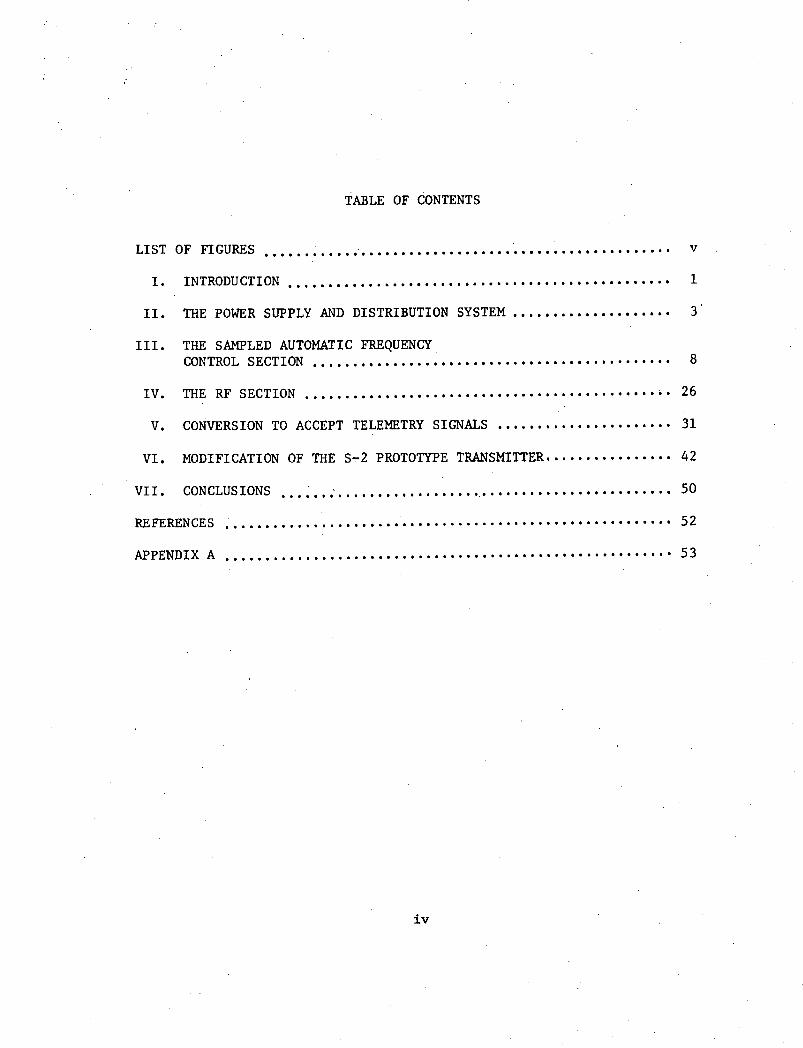
TABLE OF CONTENTS
LIST OF FIGURES .......................................... v
I. INTRODUCTION ................................................ 1
II. THE POWER SUPPLY AND DISTRIBUTION SYSTEM .... 3........ 3
III. THE SAMPLED AUTOMATIC FREQUENCYCONTROL SECTION ............................................. 8
IV. THE RF SECTION .............................................. 26
V. CONVERSION TO ACCEPT TELEMETRY SIGNALS ...................... 31
VI. MODIFICATION OF THE S-2 PROTOTYPE TRANSMITTER ................ 42
VII. CONCLUSIONS 50
REFERENCES .... ... 5.............. ....... ........ 52
APPENDIX A ..................................................... 53
iv

LIST OF FIGURES
2-1. 28 VDC regulator with thermal shutdown control ............... 4
2-2. Regulator for + 5 VDC supply ................................. 6
3-1. Block diagram of SAFC section of Transmitter ................. 9
3-2. Outputs of discriminator switch. 0.5 volts/cm vertical
scale and 10 Psec/cm horizontal scale ........................ 10
3-3. Difference of discriminator outputs shown in Figure 3-2. 0.05volts/cm vertical scale and 10 Ps/cm horizontal scale ........ 10
3-4. Signal at collectors of Q504A and Q504B during 3.5us VCO sample pulse. 0.5 volt/cm vertical scale and 2Vs/cm horizontal scale ....................................... 12
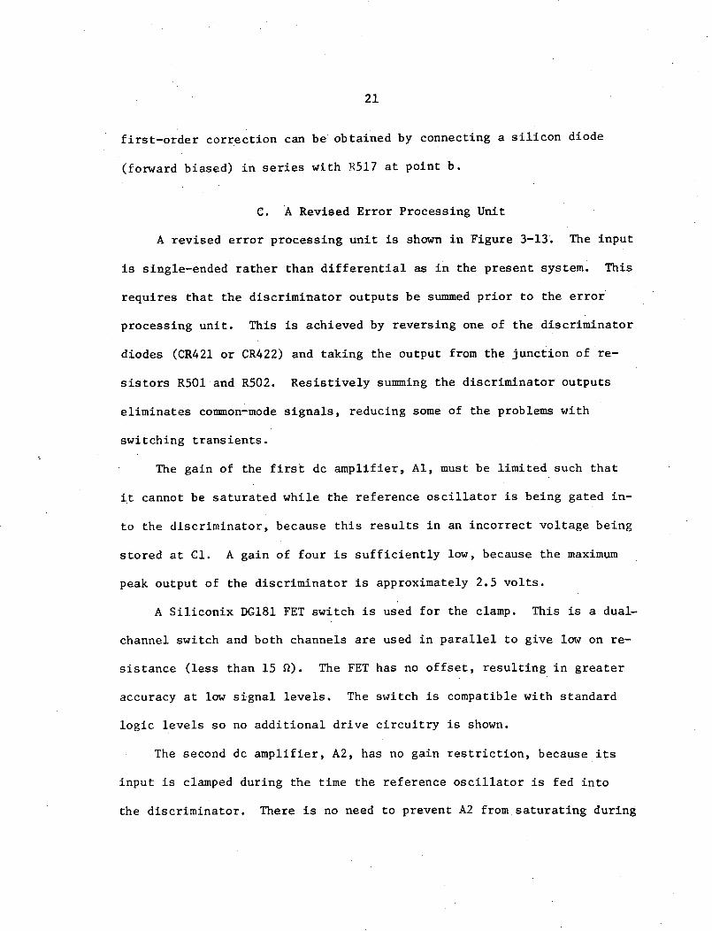
3-5. Error signal at E505 (upper trace) and output of discriminatorswitch. 1 volt/cm vertical scale and 10 Psec/cm ............. 12
3-6. Error signal at E505 (upper trace) and 2.0 Ps pulse to sampleand hold circuit. 2 volts/cm vertical scale and 2 isec/cmhorizontal scale ............................................. 13
3-7. FET chopper circuit used as discriminator switch ............. 14
3-8. Voltage-controlled amplifier used as discriminator switch.... 16
3-9. Differential output of circuit shown in Figure 3-8 duringgating with a dc differential input signal applied ........... 17
3-10. Output of MC1545 (upper trace) and gating signal (lower trace)for 200 kHz triangular waveform. 200 ns/cm horizontal scale.0.5 volt/cm (upper trace) and 5 volts/cm (lower trace)vertical scale............................................... 17
3-11. MC1545 gated video amplifier used as a discriminator switch.. 18
3-12. Output and clamping circuitry of SAFC system ................. 20
3-13. Revised error processing unit ................................ 22
v
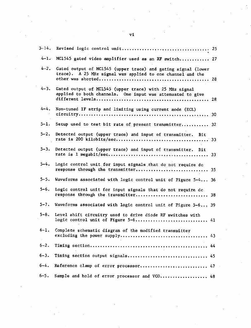
vi
3-14. Revised logic control unit ................................... 25
4-1. MC1545 gated video amplifier used as an RF switch ............ 27
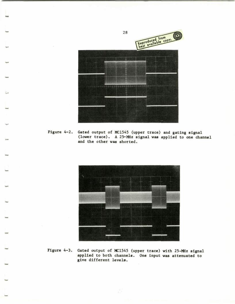
4-2. Gated output of MC1545 (upper trace) and gating signal (lowertrace). A 25 MHz signal was applied to one channel and theother was shorted ................................. 28
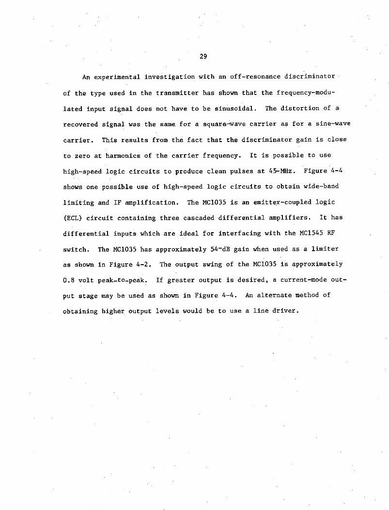
4-3. Gated output of MC1545 (upper trace) with 25 MHz signalapplied to both channels. One input was attenuated to givedifferent levels ............................................. 28
4-4. Non-tuned IF strip and limiting using current mode (ECL)circuitry ..................................................... 30
5-1. Setup used to test bit rate of present transmitter ........... 32
5-2. Detected output (upper trace) and input of transmitter. Bitrate is 200 kilobits/sec .................................... 33
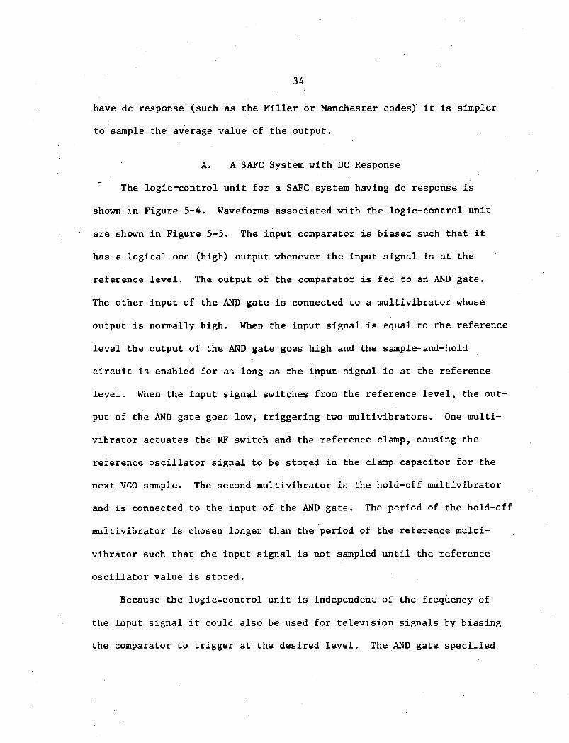
5-3. Detected output (upper trace) and input of transmitter. Bit
rate is 1 megabit/sec ........................................ 33
5-4. Logic control unit for input signals that do not require dc
response through the transmitter ............................. 35
5-5. Waveforms associated with logic control unit of Figure 5-4... 36
5-6. Logic control unit for input signals that do not require dcresponse through the transmitter ............................. 38
5-7. Waveforms associated with logic control unit of Figure 5-6... 39
5-8. Level shift circuitry used to drive diode RF switches withlogic control unit of Figure 5-6 ............................. 41
6-1. Complete schematic diagram of the modified transmitterexcluding the power supply ................................... 43
6-2. Timing section ............................................... 44
6-3. Timing section output signals................................ 45
6-4. Reference clamp of error processor ........................... 47
6-5. Sample and hold of error processor and VCO .................. 48
vii
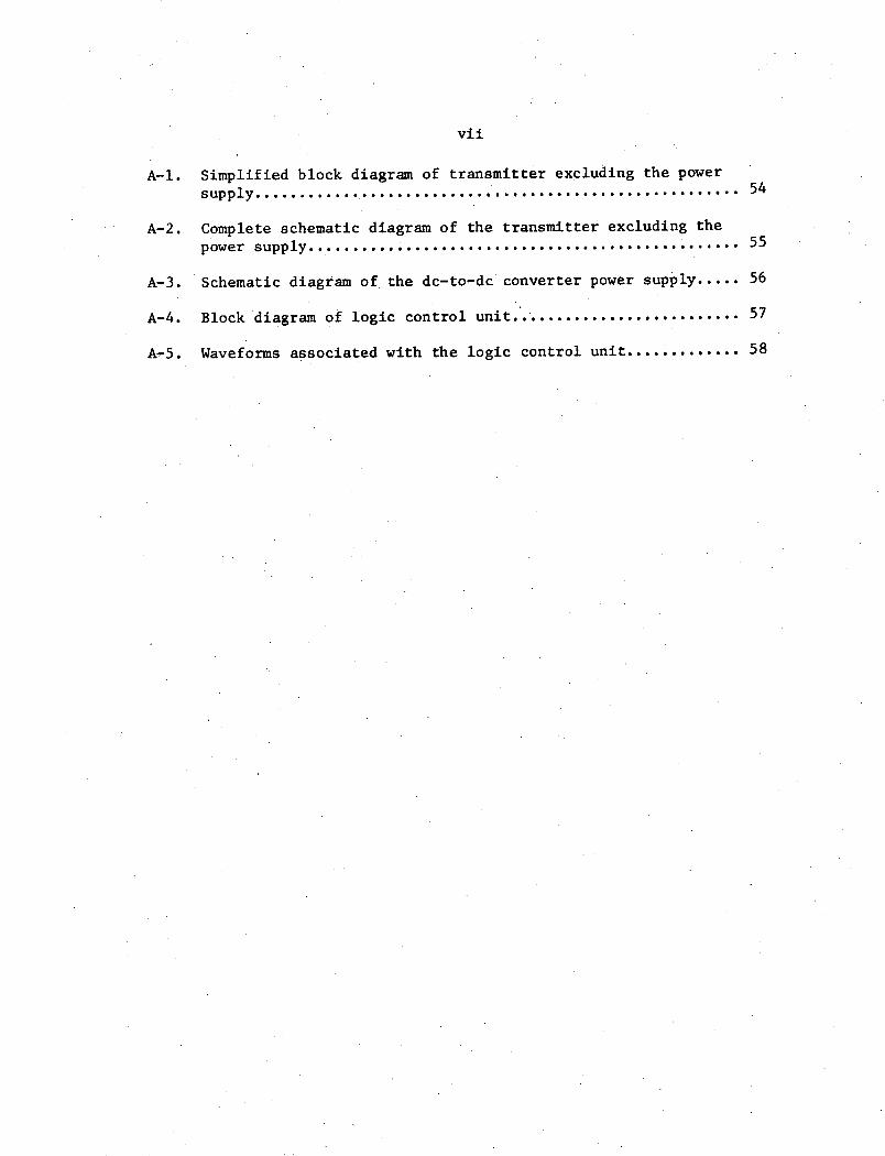
A-1. Simplified block diagram of transmitter excluding the powersupply .............. ............. ................ 54
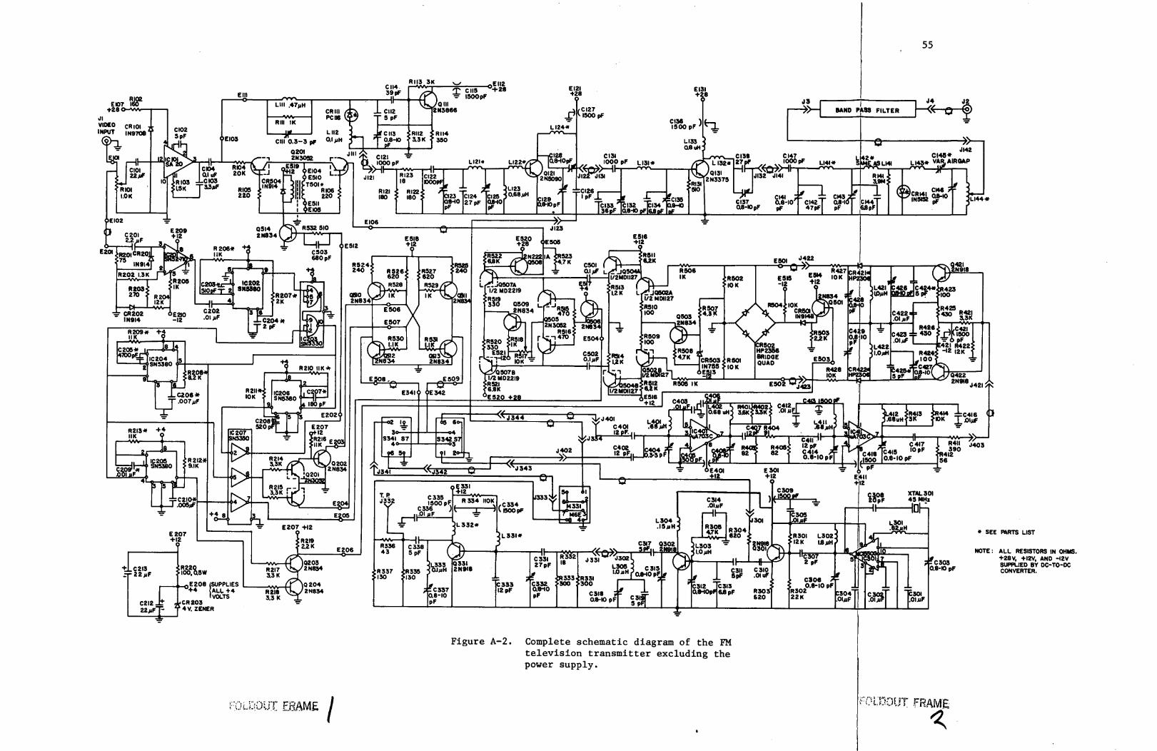
A-2. Complete schematic diagram of the transmitter excluding thepower supply............................. ......... 55
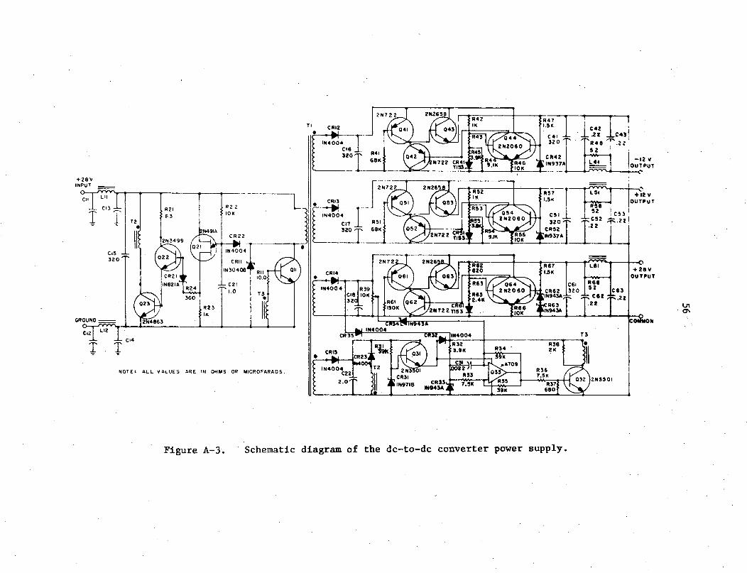
A-3. Schematic diagram of the dc-to-dc converter power supply..... 56
A-4. Block diagram of logic control unit ............... 57...... 57
A-5. Waveforms associated with the logic control unit ............ 58

I. INTRODUCTION
This report represents the results of a study made on the Auburn
University Model S-2 FM television transmitter. The objectives of this
study were:
1) To determine the performance capabilities of the transmitter,
both in its present form, and with feasible modifications.
2) To determine the modifications which may be made to the trans-
mitter to improve reliability and frequency stability.
3) To determine the necessary changes to enable the transmitter to
accept high data rate telemetry signals.
4) To examine the new devices, particularly integrated circuits,
which have been introduced since the transmitter design was
finalized to determine if any of these devices could improve
the performance and reliability of the transmitter.
The operation of the transmitter has been described in detail in
previous reports. For convenience, block and schematic diagrams and
pertinent waveforms are included in Appendix A. Unless otherwise stated,
all references to specific components or test points refer to Figure A-2
(the transmitter) or to Figure A-3 (the power supply).
Where possible, the proposed changes were breadboarded and tested.
In particular some of the changes necessary to make the transmitter com-
patible with telemetry signals were tested. This was considered necessary
1
2
because these modifications involved the use of new techniques rather
than improvements in existing circuitry.
Chapter II concerns the power supply (dc-dc converter). The primary
modifications deal with incorporating additional protective circuitry and
greater use of integrated circuits.
Changes to the AFC control section (see Figure A-1, page 54) are
discussed in Chapter III. The main intent of the modifications presented
here is to increase the frequency stability of the transmitter. Many of
these changes are possible because of the availability of new high per-
formance integrated circuits.
In Chapter IV the proposed modifications to the RF sections are pre-
sented.
The conversion of the transmitter to accept signals other than stan-
dard NTSC television signals is considered in Chapter V. The choice of
format for the signals considered was largely from reference [1] which
dealt with logical choices for a data bus on a space shuttle.
Modifications actually made on the prototype transmitter are outlined
in Chapter VI.
Conclusions are presented in Chapter VII.
II. THE POWER SUPPLY AND DISTRIBUTION SYSTEM
The present power supply performs reliably over the temperature
range of -20 to +80 degrees Celsius. Since construction of the original
prototype, Qll (Figure A-3) has been replaced with a Solitron 2N3749
transistor. This substitution was necessary to provide an adequate dis-
sipation margin at high ambient temperature. This change has been made
on transmitters Serial Numbers 2, 3 and 4, delivered to Marshall Space
Flight Center, Huntsville. Also, some filter chokes used for high-fre-
quency filtering in the +28 VDC distribution system have been replaced
with chokes having lower series resistance, thus improving regulation of
the power supply.
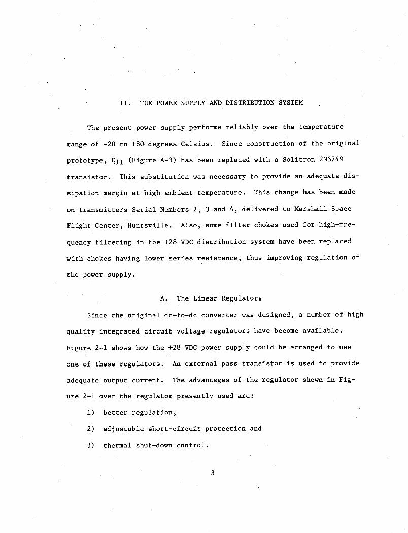
A. The Linear Regulators
Since the original dc-to-dc converter was designed, a number of high
quality integrated circuit voltage regulators have become available.
Figure 2-1 shows how the +28 VDC power supply could be arranged to use
one of these regulators. An external pass transistor is used to provide
adequate output current. The advantages of the regulator shown in Fig-
ure 2-1 over the regulator presently used are:
1) better regulation,
2) adjustable short-circuit protection and
3) thermal shut-down control.
3
-.0.4CO
cr
N
-L
OZ+
.z
oo -c44 A
c. 0Ooocl
C4w 0Cboa)'4
NC-4
fZ4
DZ
OW
D
0IL
0 >00<
-300 r
, o
0
L)
WW
W
cu-i-
1 ~L1
I
J -J
-J
_P
_
wz
.4
I
5
The most important feature is the thermal shut-down control. This
allows protection not only for the power supply, but also for the trans-
mitter if the ambient temperature exceeds the safe operating point. Re-
sistor R4 may be selected to give the desired shut-down temperature. The
MC1561 exhibits some "cycling" as the temperature reaches the shut-down
level, however none of the present +28 VDC circuits would be adversely
affected. When the temperature falls below the desired shut-down level,
the regulator will resume normal operation.
Similar circuits could be used for the ±12 VDC supplies, except that
the external pass transistor is unnecessary as the MC1561 is capable of
supplying adequate current. The same reference supply (CR2, CR3) could
be used to set the shut-down temperature, if this feature is desired for
the ±12 VDC supplies.
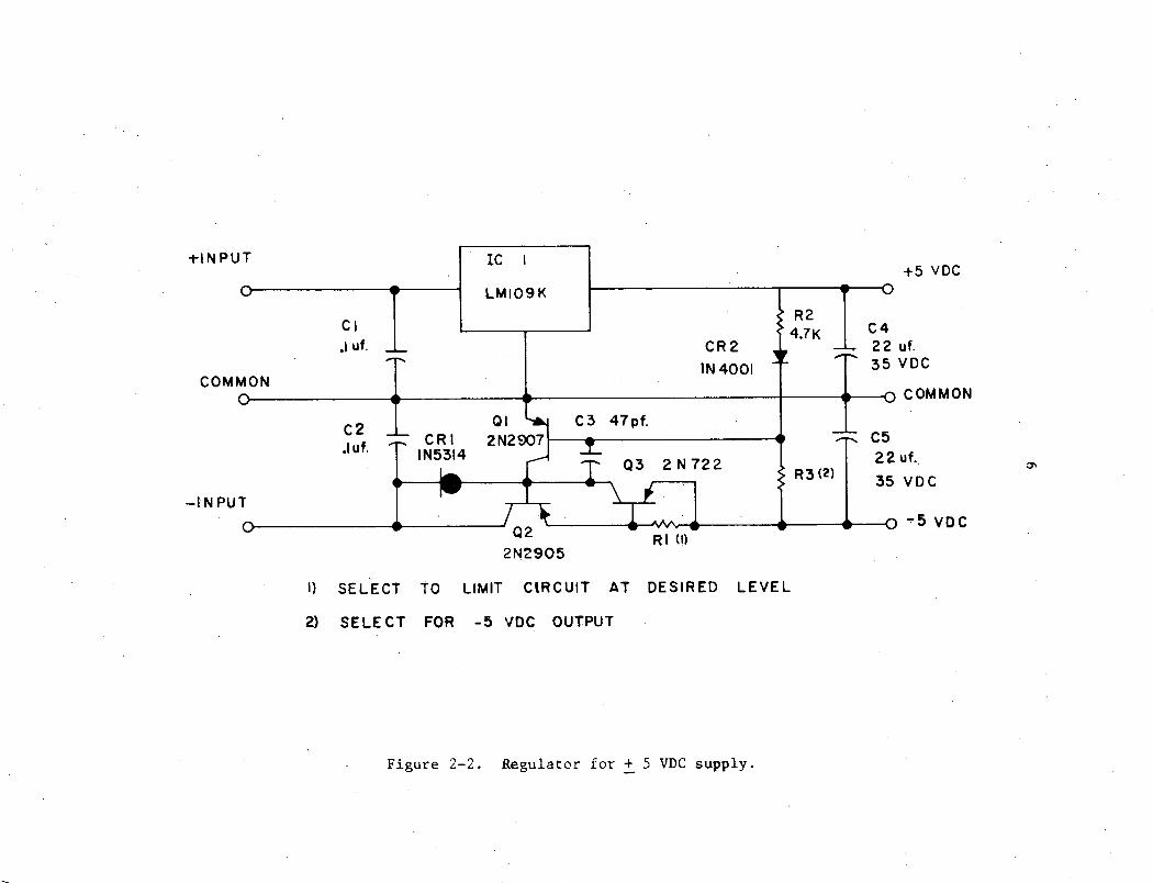
B. Additional Output Voltages
Many of the proposed changes will require ±5 VDC power supplies in
addition to the +28 VDC and ±12 VDC supplies. Figure 2-2 shows one method
for obtaining these voltages. The +5 VDC will be required to supply the
greater current, especially if TTL logic is used. The National Semicon-
ductor LM109 regulator is suitable for this supply. It incorporates both
current limiting and thermal shut-down. Because the reference for the
-5 VDC supply is taken from the +5 VDC supply, it will also be shut down
if the ambient temperature exceeds safe limits. Even if a simple Zener
regulated supply could furnish sufficient current, the shut-down feature
might make the additional circuitry of the supply shown worthwile. Short
circuit protection may be provided by proper choice of CR1.
>U')
r+
0)
u i
P4 0-
0 C
.,.;
a c
.vr N
L
O
CIA
C
) X
Nu r)
YN
%
cr
l!
Na:
a0Z
z00U
)
6
z020
.
if)
a:
>I
-J-JIAJa:wnLU
Nc\NzN
'
If
IJ
--
tr-C.
Nz
N
tZ
0Z
toa0Z'
zCcj
C1
I-a.t-I"0I
I-a:I--.
+100 C)
+Io 0L4
4ra:
00
I.-0
Uw
W
W
WJ
I--Iw
J
U) c/
L
.
6p-az
-N
06
z
yy
r1 I
l( _
7
C. The Switching Section of the dc-to-dc Converter
The unregulated voltages of the power supply will have to be in-
creased if the IC regulators are used. This can be accomplished by
increasing the number of turns on the secondary windings of transformer
T1. If the output current requirements of the power supply are increased,
a complete re-design of transformer T1 may be required. The semiconduc-
tors used can furnish substantially more current than is required now.
The 709 type operational amplifier (Q33) used in the logic control
circuitry could be replaced with either a 748, 101, or 1539 type. All
of these amplifiers are short-circuit protected and have far superior
common-mode characteristics to the 709. While the circuit is designed
to keep the 709 within its safe operating region, substitution of a newer
type amplifier will give a greater safety margin. Any of the amplifiers
listed is a direct replacement for the 709 in this application.

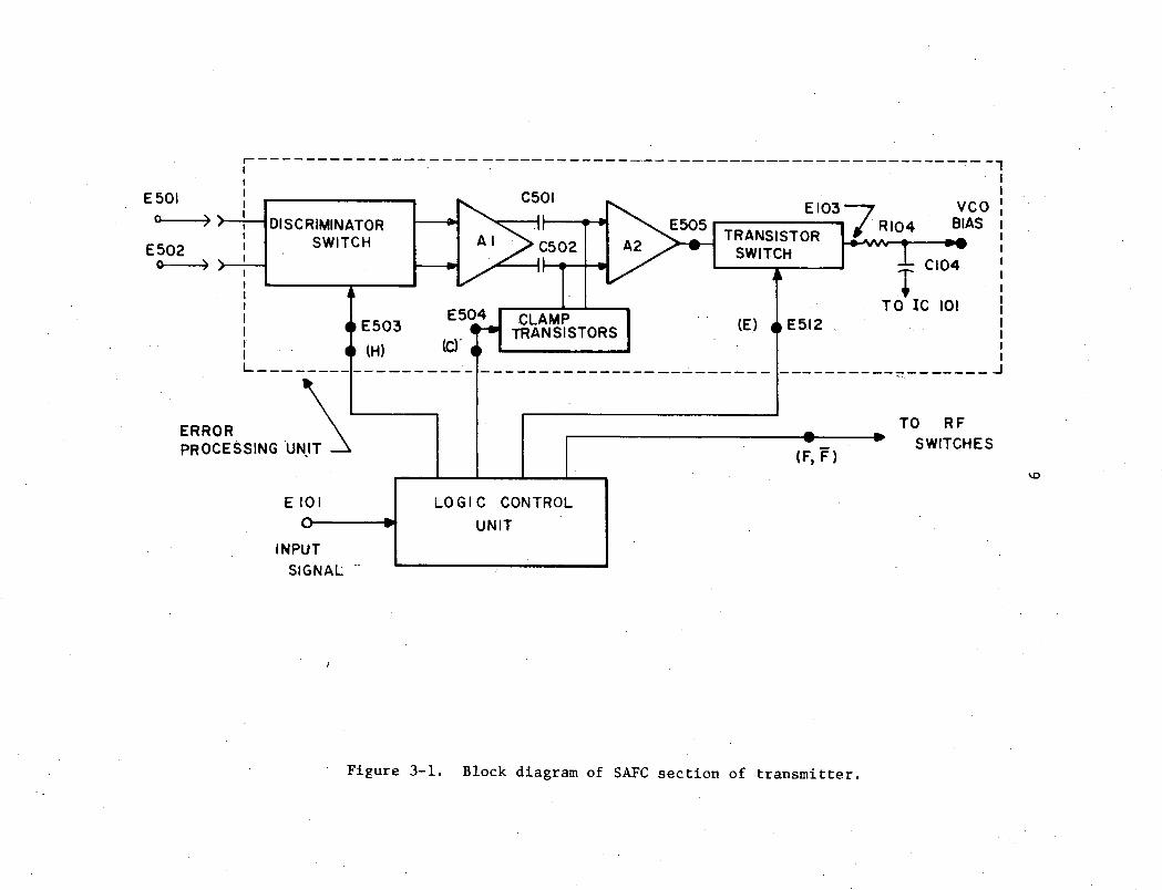
III. THE SAMPLED AUTOMATIC FREQUENCY CONTROL SECTION
A block diagram of the sampled automatic frequency control (SAFC)
section of the transmitter is shown in Figure 3-1. The SAFC section is
divided into two blocks, the logic control unit and the error processing
unit. The logic control unit provides the timing pulses which control
the RF switches and the error processing unit. Because the functions
of the logic control unit are implemented digitally, very little needs
to be done to this section to improve performance. The primary reason
for making changes in the logic control unit is to reduce package count
(by use of MSI and LSI IC's) or to interface with a new error processing
unit.
The error processing unit performs the actual corrections on the
VCO. Because this unit must handle the signal in analog form, it is
more likely to cause error than is the logic control unit. One diffi-
culty arises from the precision required of the error processing unit.
A frequency stability of 0.01% requires that the output of the error pro-
cessing unit vary less than 14 mV. Some modifications are presented for
this unit, using integrated circuits which have recently become available.
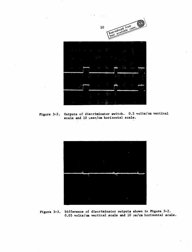
A. The Discriminator Switch
The discriminator outputs are gated by a diode quad, CR502. The
outputs of the discriminator switch are shown in Figure 3-2. The pulses
occur at the times at which the discriminator outputs are gated into the
8
r---- -
-- --
---- --
--
03(*)U
)
W
w
W
9
a,
4-J00(J4J 0 r.
CD)
U)Eo
000Ct
'-04)'4 PL
I.I.LI.
4zn V)
10
Figure 3-2.
Figure 3-3.
Outputs of discriminator switch. 0.5 volts/cm verticalscale and 10 Psec/cm horizontal scale.
Difference of discriminator outputs shown in Figure. 3-2.0.05 volts/cm vertical scale and 10 us/cm horizontal scale.
11
dc amplifier. The output of the discriminator is a constant level pro-
portional to the frequency during both the 7 ps reference pulse and
during the 3.5 ps VCO pulse because the input frequencies are constant.
In Figure 3-3 the difference in the signals of Figure 3-2 is shown. The
spikes are caused by the diode quad, due to the fact that it does not
have balanced loading on the two inputs and outputs. These spikes are
amplified by the dc amplifier which has differential inputs. Figure 3-4
shows the outputs at the collectors of Q502, the first differential am-
plifier. In Figure 3-5 the output of the second differential amplifier,
E505, is shown along with the outputs of the discriminator switch. The
error signal during the 3.5 is VCO pulse and the 1.6 Us sample and hold
pulse are shown in Figure 3-6. The minor notches in the error signal
are caused by power supply interaction and may be reduced by bypassing
the +12 VDC supply to ground at point E519. A .01 pF ceramic disc capac-
itor is sufficient.
The spikes in the error signal are integrated by R104 and C104.
Thus the effect on the frequency stability is not as pronounced as the
amplitude would indicate. However it would be desirable to revise the
discriminator switch to reduce the switching transients.
1. A Field Effect Transistor Discriminator Switch
An alternate method of gating the discriminator is to use an FET
chopper circuit as shown in Figure 3-7. The FET switch shown, a Siliconix
DG190, is a dual channel unit which may be controlled by standard logic
levels, eliminating the need for driver, or level shift, circuitry. Be-
cause the present discriminator switch is activated by a +12 VDC signal,
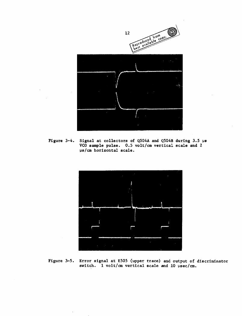
Figure 3-4.
Figure 3-5.
Signal at collectors of Q504A and Q504B during 3.5 UsVCO sample pulse. 0.5 volt/cm vertical scale and 2us/cm horizontal scale.
Error signal at E505 (upper trace) and output of discriminatorswitch. 1 volt/cm vertical scale and 10 usec/cm.

13
Figure 3-6. Error signal at E505 (upper trace) and 2.0 ps pulse tosample and hold circuit. 2 volts/cm vertical scale and2 Usec/cm horizontal scale.

14
w-1
><
W
Zj
,O
z0w
0
o
4 cr
_ O
--
X
u0
Z
o al
! oJ )
oIZ
41
0 0
H0
Ul p-
0Ln cr
Dw
W
$-4
0
o~ U.
o ( U
U
-O
:
+
0
x '-
0 0
U
>' C
-- -
)( L
(
---
1 C
C
OH
'H~~~·r
-gd')
C,,~~~~~~~~~~~~~~~~~~~~~~~~~r
E5
U)0--
0UC,I-

15
a pad is shown at the control input. This could be eliminated if the
supply voltage at E207 were changed to the logic level. The switch is
operated as a series-shunt chopper.
2. A Voltage Controlled Amplifier as a Discriminator Switch
A second method of gating the discriminator is to control the gain
of the first dc amplifier pair (Q502). A convenient method by which
this may be done is to vary the bias current. Since an active current
source (Q503, CR503, R507, R508) is used to provide the bias current,
this could be accomplished with a minimum number of circuit changes. To
test this technique, the circuit of Figure 3-8 was constructed. Figure
3-9 is the signal viewed at the differential output of the circuit of
Figure 3-8 during gating with a dc differential input signal applied. The
output contains only a small amount of overshoot which decays to the
steady-state value within 300 ns after application of the gating pulse.
This same technique was used on a commercially available product,
the Motorola MC1545 gated video amplifier. This amplifier has two dif-
ferential inputs and a differential output. Channel selection is con-
trolled by the voltage applied at a gating input. The gate voltages are
compatible with standard logic levels. Figure 3-11 shows a discriminator
switch using this amplifier. In some instances it may be necessary to
pad the input to avoid overload. Figure 3-10 shows the gated output of
the MC 1545 with a 200 kHz triangular input signal.

16
0N +(%1
IlF)
Ve)
_DV(D
0
I-L)
U)
O,]N
c8n
UJa
or
W
_ N
I---Z
CD
-
oaN
u4J3"o0-iE0
sw
,-4co
IVagI0u0I0a)
-H :jCL
· .o

Figure 3-9.
Figure 3-10.
Differential output of circuit shown in Figure 3-8 duringgating with a dc differential input signal applied.
Output of MC1545 (upper trace) and gating signal (lowertrace) for 200 kHz triangular waveform. 200 ns/cmhorizontal scale. 0.5 volt/cm (upper trace) and 5 volts/cm(lower trace) vertical scale.

4N0a0H
rt,c
r
an an
L& w
18
mD
aa
04
U OL(
: CIow
r_0 ,4r-Cd
0 C)
$4aa)co:oa).,4 -4r(60
Ln
-4ur
+-
II
!'-
H~

B. The Clamping Circuit and DC Amplifier
The reference-clamp and the output stage of the dc amplifier are
shown in Figure 3-12. During the 7 ps period when the reference oscil-
lator is gated into the discriminator, the clamp transistors, Q505A and
Q505B, are turned on such that C501 and C502 are charged to a voltage
proportional to the reference frequency. After a 28-ps interval, the
3.5-ps VCO pulse is gated into the dc amplifier from the discriminator
and a voltage proportional to the difference is measured at the output.
If for some reason the signal is interrupted, the bias currents for
Q507A and Q507B, IA and IB, would cause C501 and C502 to charge (or dis-
charge) such that a false correction voltage would be developed on the
next sync pulse. In addition, since the hold capacitor is biased to a
definite level (+14 VDC) the VCO will gradually drift off frequency if
the signal is interrupted. Finally the method by which the nominal
+14 VDC bias is obtained for the VCO is to adjust the current source of
the output stage (R517, R518, Q509). Because the current provided by
this source is a function of the base-emitter voltage of a transistor,
it is temperature sensitive. The temperature coefficient for a silicon
transistor is -2 mV/°C. Over a 1000 C range (-200 C to +800 C) this causes
a 0.2 VDC change in VBE for Q509. This would correspond to a change in
the error voltage of approximately 0.5 volt. The gain of the VCO
(Hz/volt) is such that the specified tolerance would be equivalent to a
14 mV change in the error voltage. While this change is within the
SAFC feedback loop, and is corrected, the temperature stability of the
system would be improved if this error could be compensated for. A
19

20
C
n0 0a
o N
U-) F-
rr'L1
4
LO
0 O
'
LO
0U,
4cNC-
'"
' ::
r- ln0aoOf
C-
C~J+
0041 (Jr~
a)U)
0 n>1
.rCo
44 0 4i
C: og:
41
s0
cu')
tno zO
Cd
r.la)
4
U-)c
21
first-order correction can be obtained by connecting a silicon diode
(forward biased) in series with R517 at point b.
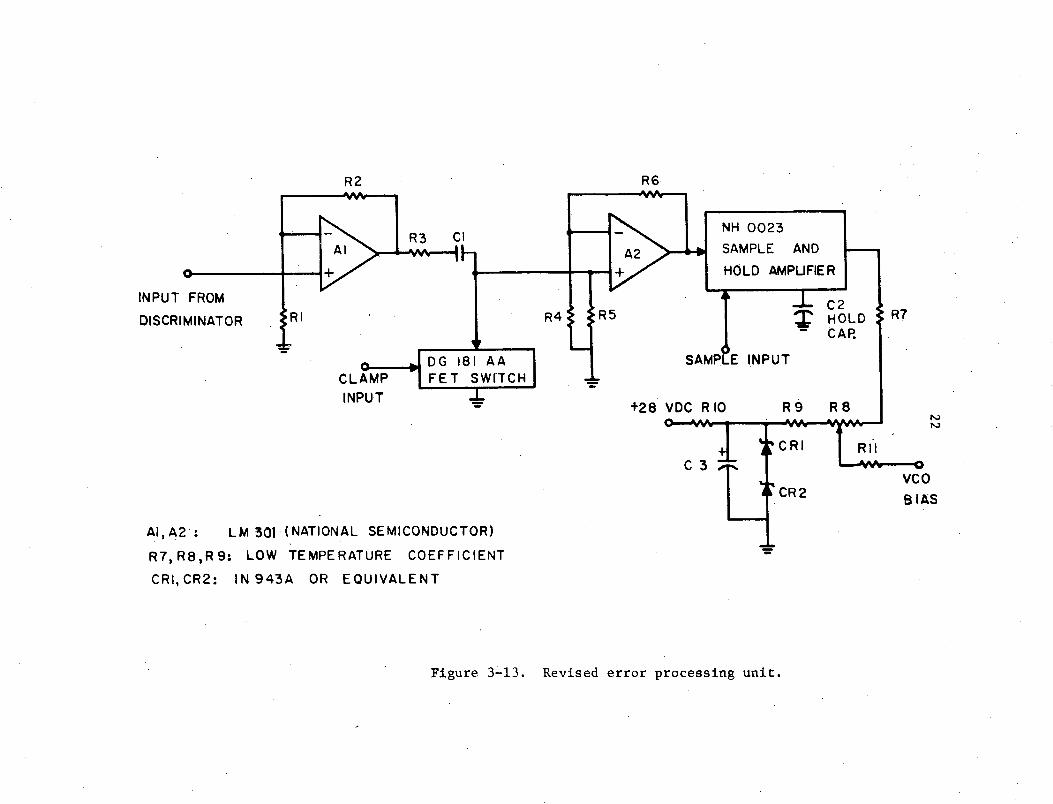
C. A Revised Error Processing Unit
A revised error processing unit is shown in Figure 3-13. The input
is single-ended rather than differential as in the present system. This
requires that the discriminator outputs be summed prior to the error
processing unit. This is achieved by reversing one of the discriminator
diodes (CR421 or CR422) and taking the output from the junction of re-
sistors R501 and R502. Resistively summing the discriminator outputs
eliminates common-mode signals, reducing some of the problems with
switching transients.
The gain of the first dc amplifier, Al, must be limited such that
it cannot be saturated while the reference oscillator is being gated in-
to the discriminator, because this results in an incorrect voltage being
stored at C1. A gain of four is sufficiently low, because the maximum
peak output of the discriminator is approximately 2.5 volts.
A Siliconix DG181 FET switch is used for the clamp. This is a dual-
channel switch and both channels are used in parallel to give low on re-
sistance (less than 15 S). The FET has no offset, resulting in greater
accuracy at low signal levels. The switch is compatible with standard
logic levels so no additional drive circuitry is shown.
The second dc amplifier, A2, has no gain restriction, because its
input is clamped during the time the reference oscillator is fed into
the discriminator. There is no need to prevent A2 from saturating during
22 a,
O
4>
im
Nar
0.
z
00a+ OD
cl
2 t)
RQ a.
J Jz0
-
a:0
0 4
n,- Z
LL
_-n
(Mcru
0toI,
4.cn 000 .,UoaQ)
ULJ I-
0 -
o L
.
I
I--
Z
Z>
0 Z
e .
W2 9
Z
Z-.-
.
z .
oa
:
-un-
C
-
A,
c)(4Sw0PH FX
23
the VCO sample time since saturation of A2 causes a maximum correction
signal to be applied to the VCO, resulting in the error being reduced
until saturation no longer occurs.
The sample-and-hold amplifier is a National Semiconductor NH0023.
This circuit uses MOSFET's in the sample circuitry to achieve very low
leakage and has a buffered output. The sample circuitry is compatible
with standard logic levels. A resistive network is used at the output
of the SAH amplifier to level shift to the approximately 14 volts needed
to bias the VCO. R8 is adjusted such that proper bias is obtained with
zero output from the SAH amplifier. Besides operating the error-pro-
cessing circuitry in the middle of the active region, this insures that
the transmitter will continue to operate open loop if the SAFC system
fails or if the sync signal is lost. A temperature-compensated Zener
diode is used to provide isolation from the +28 VDC supply.
The revised error-processing unit does not incorporate a discrimi-
nator switch at the input because the SAH amplifier specified has very
low feedthrough in the off state. Should a discriminator switch be
needed for critical applications, either of the circuits shown in Figures
3-7 and 3-10 could be used. If the FET switch is used, a single-channel
unit could be substituted for the dual-channel unit shown.
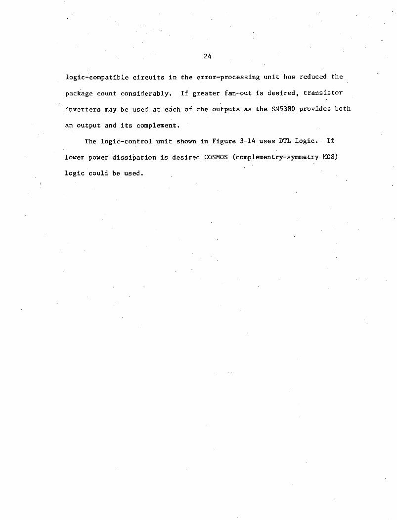
D. The Logic Control Unit
A revised logic control unit, based on the assumption that no dis-
criminator switch is needed, is shown in Figure 3-14. The use of
24
logic-compatible circuits in the error-processing unit has reduced the
package count considerably. If greater fan-out is desired, transistor
inverters may be used at each of the outputs as the SN5380 provides both
an output and its complement.
The logic-control unit shown in Figure 3-14 uses DTL logic. If
lower power dissipation is desired COSMOS (complementry-symmetry MOS)
logic could be used.
w0ZwwLU
o-Z
P(.
0o, 0 n
-..O
Z
C-)
un 4U
a
>~
+
-i--Is.I
O
->
,.->
2'._
N0to
L)
I-IV)
.
25
T oZwU
J 4
.Jo
OIO
u
I
I
I--0 0
o t
I~d':::
-,40,--IOC)
I-I
0-IelarQ)
04 -
0OD
0 0Z
_ 4t
0
0 g0
n Z
_ Cn
I
UO-i
13 ZQ
- (Dt:iv,
1
He
I.
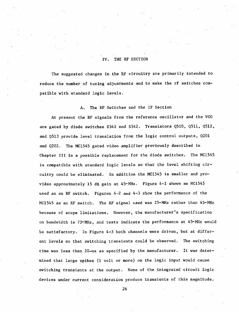
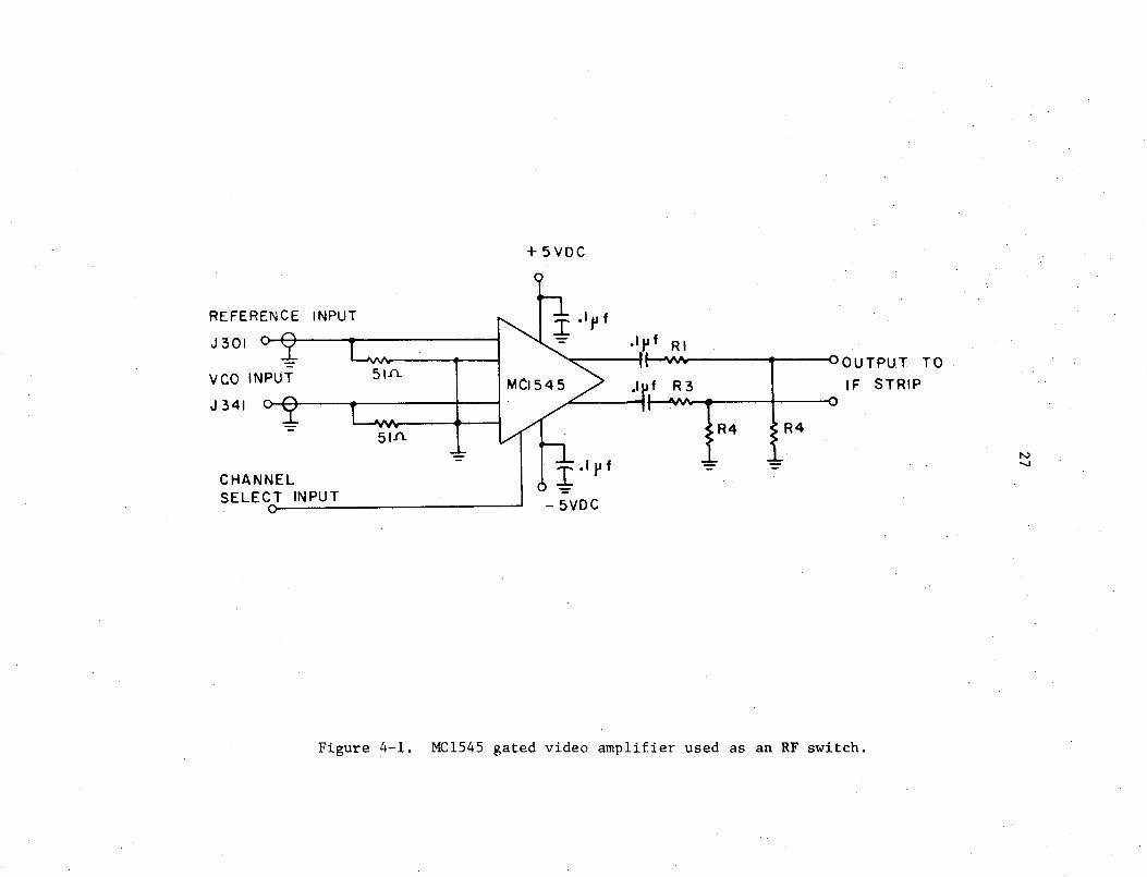
IV. THE RF SECTION
The suggested changes in the RF circuitry are primarily intended to
reduce the number of tuning adjustments and to make the rf switches com-
patible with standard logic levels.
A. The RF Switches and the IF Section
At present the RF signals from the reference oscillator and the VCO
are gated by diode switches S341 and S342. Transistors Q510, Q511, Q512,
and Q513 provide level translation from the logic control outputs, Q201
and Q202. The MC1545 gated video amplifier previously described in
Chapter III is a possible replacement for the diode switches. The MC1545
is compatible with standard logic levels so that the level shifting cir-
cuitry could be eliminated. In addition the MC1545 is smaller and pro-
vides approximately 15 dB gain at 45-MHz. Figure 4-1 shows an MC1545
used as an RF switch. Figures 4-2 and 4-3 show the performance of the
MC1545 as an RF switch. The RF signal used was 25-MHz rather than 45-MHz
because of scope limitations. However, the manufacturer's specification
on bandwidth is 75-MHz, and tests indicate the performance at 45-MHz would
be satisfactory. In Figure 4-3 both channels were driven, but at differ-
ent levels so that switching transients could be observed. The switching
time was less than 20-ns as specified by the manufacturer. It was deter-
mined that large spikes (1 volt or more) on the logic input would cause
switching transients at the output. None of the integrated circuit logic
devices under current consideration produce transients of this magnitude.
26
27
0
a-
D i,
0 -
ci 'acoU,
$-4,4
r=.ToC,
0Q)
-ia00In-sIn
L_)+
28
1 " 1 . : . . 1.1 ' ' • — ' • - . - . — P W . . . - P — P . . » . . . . . , . • l - . - l ^ — • • .......... -
p " ; ; • "•-:";
i
Figure 4-2. Gated output of MC1545 (upper trace) and gating signal (lower trace). A 25-MHz signal was applied to one channel and the other was shorted.
Figure 4-3. Gated output of MC1545 (upper trace) with 25-MHz signal applied to both channels. One input was attenuated to give different levels.
29
An experimental investigation with an off-resonance discriminator
of the type used in the transmitter has shown that the frequency-modu-
lated input signal does not have to be sinusoidal. The distortion of a
recovered signal was the same for a square-wave carrier as for a sine-wave
carrier. This results from the fact that the discriminator gain is close
to zero at harmonics of the carrier frequency. It is possible to use
high-speed logic circuits to produce clean pulses at 45-MHz. Figure 4-4
shows one possible use of high-speed logic circuits to obtain wide-band
limiting and IF amplification. The MC1035 is an emitter-coupled logic
(ECL) circuit containing three cascaded differential amplifiers. It has
differential inputs which are ideal for interfacing with the MC1545 RF
switch. The MC1035 has approximately 54-dB gain when used as a limiter
as shown in Figure 4-2. The output swing of the MC1035 is approximately
0.8 volt peak-to-peak. If greater output is desired, a current-mode out-
put stage may be used as shown in Figure 4-4. An alternate method of
obtaining higher output levels would be to use a line driver.

0
I--z
,- 2
30a-3 o
N
o.0
tcO cC0
cx C
L
_ 0U
u0. .
N
>
(0
n--
l( "
(
-- w
.
Io -
U' o
_-C
: C
cr
-
c~
~~
~N
0I
O
01
· rl~~~~~~~~~~~~~~~~~~~~~~~~~~~~~~-j
=r~
~~
~~
~~
~~
~~
~~
~~
~~
~~
~~
~-
I-z
Ir
V. CONVERSION TO ACCEPT TELEMETRY SIGNALS
The present sampled-automatic-frequency-control (SAFC) section is
actuated by the sync pulses which are present in NTSC television signals.
Most telemetry codes [1] now being considered for high-data-rate trans-
mission do not contain sync pulses. If the transmitter is to handle
these codes the SAFC section will have to be redesigned.
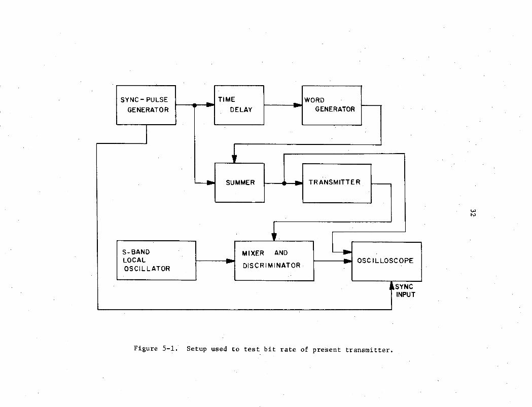
In order to determine the ability of the transmitter to handle
binary signals, the test set-up shown in Figure 5-1 was used. A pulse
generator was used to provide pulses corresponding to the video sync
pulses and to trigger a word generator. A 4-ps time delay was placed
between the sync-pulse generator and the word generator. This time delay
allows the correction voltage to be applied to the VCO during the time of
the base line rather than during the signal. Figures 5-2 and 5-3 show the
transmitter input and discriminator output for bit rates of 200 kilobits/sec.
and one megabit/sec. The upper limit of the word generator was one mega-
bit/sec., however, the pulse shape at this rate indicates that bandwidth
of the RF sections should be sufficient to handle signals of two to three
megabits/second.
Two basic SAFC systems were investigated. The first is for signals
for which dc response is necessary. For these signals it is necessary
to sample the VCO output at only one level such that the signal is
clamped to this level. For signals not requiring the transmitter to
31
32
4,
.,J
-410-J U,
4.).aJ04J 0.4-.0.:34i14bo
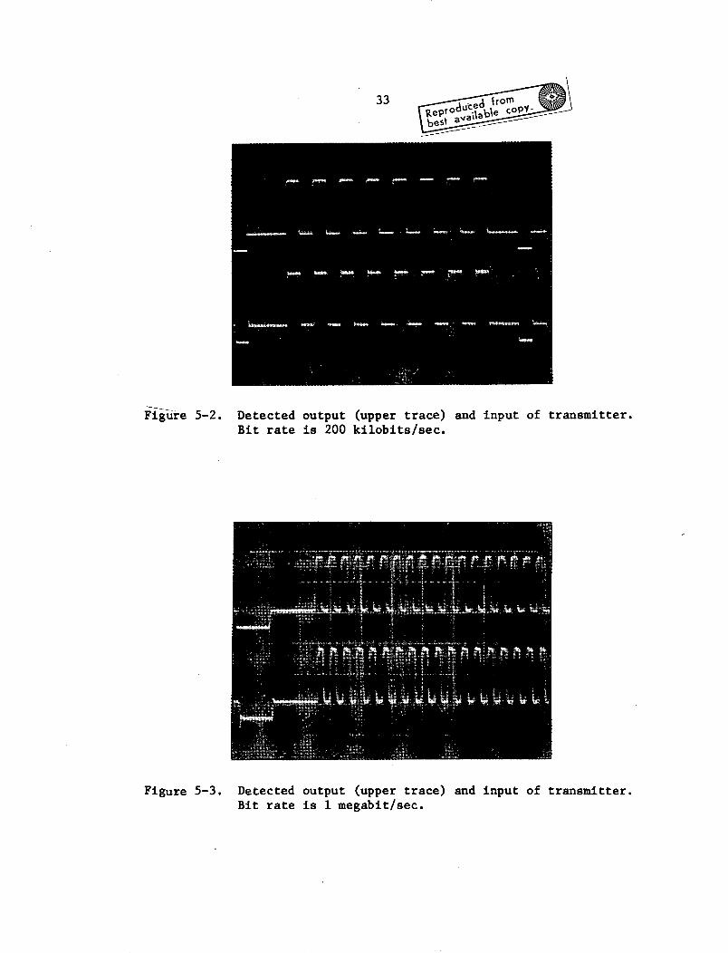
Figure 5-2.
Figure 5-3.
Detected output (upper trace) and input of transmitter.Bit rate is 200 kilobits/sec.
Detected output (upper trace) and input of transmitter.Bit rate is 1 megabit/sec.
34
have dc response (such as the Miller or Manchester codes) it is simpler
to sample the average value of the output.
A. A SAFC System with DC Response
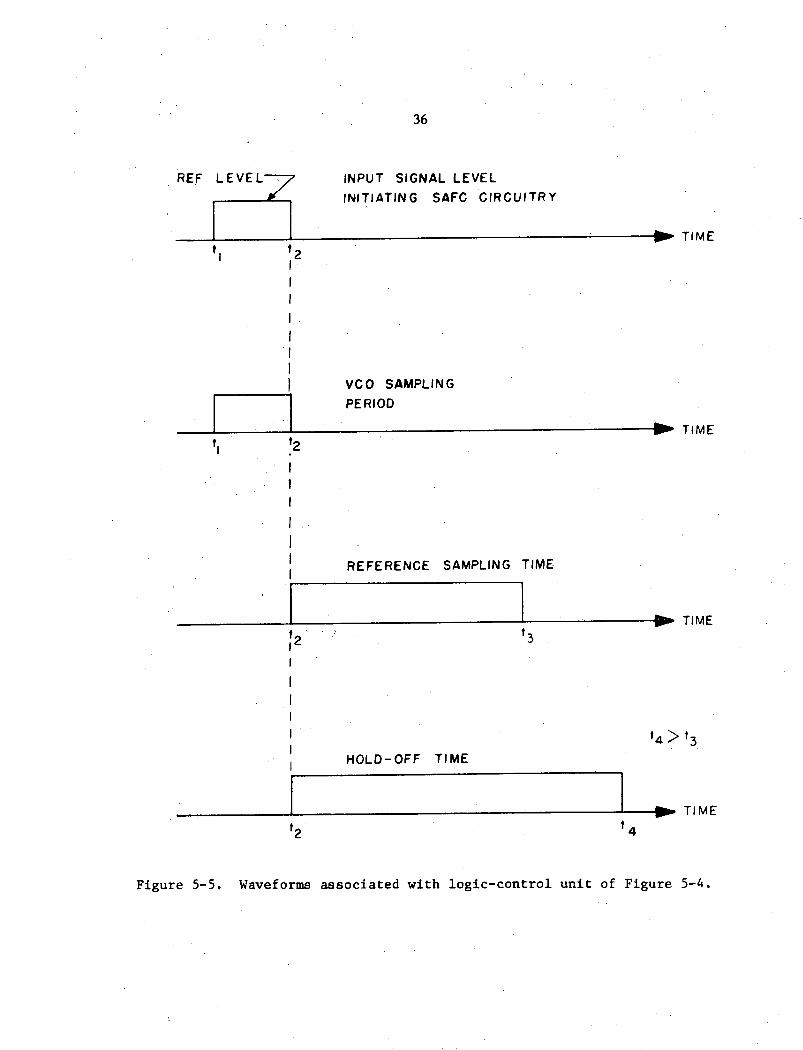
The logic-control unit for a SAFC system having dc response is
shown in Figure 5-4. Waveforms associated with the logic-control unit
are shown in Figure 5-5. The input comparator is biased such that it
has a logical one (high) output whenever the input signal is at the
reference level. The output of the comparator is fed to an AND gate.
The other input of the AND gate is connected to a multivibrator whose
output is normally high. When the input signal is equal to the reference
level the output of the AND gate goes high and the sample-and-hold
circuit is enabled for as long as the input signal is at the reference
level. When the input signal switches from the reference level, the out-
put of the AND gate goes low, triggering two multivibrators. One multi-
vibrator actuates the RF switch and the reference clamp, causing the
reference oscillator signal to be stored in the clamp capacitor for the
next VCO sample. The second multivibrator is the hold-off multivibrator
and is connected to the input of the AND gate. The period of the hold-off
multivibrator is chosen longer than the period of the reference multi-
vibrator such that the input signal is not sampled until the reference
oscillator value is stored.
Because the logic-control unit is independent of the frequency of
the input signal it could also be used for television signals by biasing
the comparator to trigger at the desired level. The AND gate specified

I-Jo
2
aoz.- 4[In
0e
I.4cr0I- 40 4 49
-i=1-2-- -Z
CL C
Z
U
to0-jJ
O
35
V(
I-
'0X
U
v) oz_
04Q
IU
. 0
LL. C I -
a ;:
O
II a
-F
i
rm
o
I')
z.U)
o¢)
-W
-H
0U
O,
-H
0 4
-H
0O
d
OQ
S
0)54bo.,
4rZ
4
D
36
INPUT SIGNAL LEVEL
INITIATING SAFC CIRCUITRY
TIME
VCO SAMPLING
PERIOD
_'" TIME
REFERENCE SAMPLING
,t2 - t 3
I
HOLD-OFF
I2
TIME
It
Waveforms associated with logic-control unit of Figure 5-4.
REF
tI t2
I
rTIME
-_W TIME
t 4 > t 3
_- TIME
4
I~~~~~~~~~~~~~~~~~~~~~~~~~~~~~~~~~~~~~ I
14
Figure 5-5.
t I t 2
I
.I.
I
37
is a Schottky-clamped TTL gate with a maximum propagation time of 7-ns.
The same error-processing section as used for television signals may be
used.
This logic-control unit may be used with the error processing unit
shown in Figure 3-14 and the RF switch shown in Figure 4-1. If it is
used with the present error-processing unit the output to the RF switches
will have to be level-shifted.
B. An SAFC System with Average Response
For codes which do not require that the transmitter maintain response
down to dc, the average value of the detected VCO output may be used to
make the correction. The average value may be obtained by inserting
a low-pass filter at the discriminator output. With the outputs resis-
tively summed, this can be accomplished by connecting a capacitor from
the output to ground. The time constant should be selected sufficiently
low that the signal is not attenuated.
The sampling technique is retained in order that the same limiters,
discriminator, and error-processing section may be used for both the
reference oscillator and the VCO signals.
The logic-control unit for the average responding SAFC is shown in
Figure 5-6. The waveforms associated with the logic-control unit are
shown in Figure 5-7. The 709 operational amplifier is used as an oscil-
lator to provide the clock signal for the system. The clock signal is
fed through a buffer amplifier to a divide-by-10 counter. The divide-
by-10 output of the counter is used to control the RF switches. The

4o-i04JJ
U,
CO
C
COO
(0
4-i
4-i uECu
Cd 0
04-i
-0
u I
0C
U,
0 4
4-4 0 ow
u)4IS
*,{ 0a,
O b0
X,4
()0U'A +

39
BUFFERED
CLOCK OUTPUT
H.n n n P n n n nnI
IOUTPUT
RF
TO
StIlTCHE Sa
H I
I 1
OUTPUT i TO
REFERENE CLAMP
I II I
.I I
I II I
I ...II II IH iI I1~~~~~7~
-_ TIME
w TIME
_ TIME
- TIME
OUTPUT TO
SAMPLE-AND-HOLD
- TIMES5
Figure 5-7. Waveforms associated with logic-control unit of Figure 5-6.
SI
S2
S3
S4
t
IIIII
IIIII
I
I
III
III !
II
7
I

40
counter shown also has a divide-by-4 output. The divide-by-10 and divide-
by-4 outputs are used to drive a quad NAND gate which produces the drive
signal for the reference clamp and the sample-and-hold circuit. The
clamp and sample pulses are spaced within the RF switch outputs so
as to avoid problems with switching transients.
The clock rate is not critical as long as it is substantially lower
than the signal frequency to avoid interference problems. A value of
5 kHz was chosen as a reasonable value.
The logic-control unit shown in Figure 5-6 may be used with the
error-processing unit shown in Figure 3-13. The signal supplied to
gate the RF switches is compatible with the MC1545 gated video ampli-
fier. In order to drive the diode switches (S341, S342) presently used,
additional circuitry is needed. This circuitry is shown in Figure 5-8.
Capacitors were used to provide the level shift. This technique pro-
vides the proper dc voltages at the switches, because the input signal,
S-2, always has a 50% duty cycle.
The logic-control unit shown in Figure 5-6 and the error-processing
unit shown in Figure 3-13 were breadboarded and tested on the S-2 trans-
mitter prototype. The results were satisfactory.

-jZ
ID-0
V)I-
LL
41
Co
clIVno
0J-
C
)
N-
Z.>.N
,1qCD
+
OCD
Wr
O't-)
Uc
U4-J
-4a)CD
I
4- Q
.-4
rL
u0
r-U'4baC
.H
J o
a)o
.4-4
d,4r fli
ooa)00.-J4

VI. MODIFICATION OF THE S-2 PROTOTYPE TRANSMITTER
The studies described in the foregoing chapters have culminated
in the modification of the S-2 prototype transmitter to enable it to
handle telemetry signals and to improve its frequency stability. Modi-
fications include complete replacement of the timing and error-pulse
processing sections and alteration of the VCO and discriminator circuitry.
A schematic diagram of the modified transmitter is shown in Figure
6-1. This should be compared to the schematic diagram of the unmodified
transmitter, Figure A-2.
In the unmodified transmitter the horizontal sync pulse was stripped
from composite video and used as the reference for generating all the
timing pulses.
The new timing section is shown schematically in Figure 6-2.
The reference for generating all the timing pulses is the clock pulse
from an oscillator utilizing a 709 operational amplifier. All the
timing pulses are generated by counting down that reference clock pulse
train. The timing section output signals are shown in Figure 6-3.
Except for output buffering the new timing section is identical
to that shown in Figure 5-6. Section B of Chapter V contains a dis-
cussion of the operation of the circuitry.
The discriminator was altered in two ways. The discriminator
switch, the CR502 diode quad in the unmodified amplifier, was eliminated.
This simplification is possible because the good signal feed through
42
i>S
-o
0 >-# >
1I-- m
E 40
oo W
:i 5T
1 J J
csi O
4 .5 A
*(
It-ao I
zI.a
1,
''
Cl- \V
-
o 1n0
e~
:N
-_
-i
U.
-.
CL
~~
~~
~~
~~
~~
~~
~~
l
w8 tau.CL
N
2ow
d
N
N
ICI oz0
-
I
-I
-if)d '
E
riL
w
I x-1F--I
-H--
;' T_11,
N
EZ
a11+o IL1
==
10-
Na-
onT Qa
|) -I
I I
= a'a
Ininul A
w
Cpl.~
~~
~~
~.
-V .IV
I 'i
I I
01
cd ~ *
co
<F ?
S~
~~
~U
U~
( i60
oI'
4e) SS
rA$a tS
''
on
f~~q "'
98
r
--II ~i"
-
HI
,OziM
CE
Ia-
i -
vo ir
4.-
0-
OSD
e1
.
!iu-v
I I07
0
ox~
~
0
-J zk
_Ia
1-
Mo
IL0
~z~
~
In
0i.N
U.
O
a d
3
0CI
H
-^4
C4
i1'
U)
-=0
t10
i IL
Uo -
,,,0
eo!
IIW.
L U uO o
8ES
7*21 o
--
8"Fv ~I
if)r--if
1 *1
n
11 I
I (I
<
I
4 w
la n
r
U) c
I-0z
0 a)
;IT
m* 1 C,
=Ctoa.
-J
-E, -
-II
N
OR
Ii.
8Mue.0
IL
a R
o 1oR
I 105
InOR
UN
U
oNnEN
U. O
Ia
ldcm
11 -I
O
I,
IL
~~O o~o
Em
if) ~ ~
~ ~
~ ~
~ i
4.~
~~
~~
~~
~~
~~
~~
.
· "J
ncr~JR~io
to ~ ~
~ ~
o
w4-
r7- -M Po
Wl
,O ~
~ ,
MO
~~
L
T- Uo~~~1111
)it0
ow0I -wC
hz
M 1
to 2
ml
M~
if)
In
ton
k n
o in C4 R
-_.
-It
--45".'
?
wi'";-1·
P "i
;,..d
LL:
' 0
,l·
HII&
X
rC4-o
--4
cJ
bo OD
o a)aJ
-rl ct-
-i00 X 4-1
-H
4-J
0 ) -H
-
C)4 r
-1.
-I 4.4
g4
090)
0 0o ·r
orC
; fi
IQ)5-.
b E
O
S-w
4.i,
9 7
;;S;
Z W
0
I-
511- Rw� i
,, ·r
0It~
I'
I
\\Rz
III
ill<4
0-,4ua-)C
)oC vl
"1-4 SH rzEq
F-4
1i:I Za4
0)
PL4

o-c
O
box
01
I o
z
o4
4w
0
a. .4U
oa,
002d 5r
45
LL
QL-
0
U)wUI Or
U)
0I-- Hif A>
To
I--00wUL
U)
i. I>
NU)
n..C
A4vU
)I)U
)
46
performance of a sample-and-hold unit used in the error-processing
system makes it unnecessary to gate off the discriminator output be-
tween samples.
Reversal of discriminator diode CR422 allows the outputs from
the two discriminator halves to be resistively added rather than
differentially subtracted to obtain the discriminator output. Con-
siderable circuit simplification results.
The new error-processing section is, except for the output feed
arrangement to the VCO, the same as that shown in Chapter III, Section
C. That section contains a discussion of the operating principles
of the new circuitry. Figure 6-4 shows the clamping portion of the
circuitry while Figure 6-5 shows the sample and hold, output feed to
the VCO, and the VCO.
The error signal, output of the sample and hold, is amplified
and fed directly to the VCO. In the unmodified transmitter, the er-
ror signal passed through a transistor switch, Q201, which gated the
error signal into the VCO only during the time when the VCO RF sample
was being processed. Use of a sample-and-hold function instead of
just a sample function eliminates the need for gating the error signal
into the VCO.
A dc voltage is still used to set the VCO frequency to its nominal
value when the error signal is zero volts. As before, this allows
for maximum dynamic range in the AFC circuitry. The source for this
dc voltage is now a part of the VCO rather than a part of the error
processor output circuitry.
The degree to which the SAFC loop is able to stabilize the VCO

N
..I
oc 0W
aH
wnE
47
:0to
en
ILto
NV
)N
Nsr
toO
L
0 :t
1o0Inen0oroU0o la1o 01-4
44a0Uwqa,
a)skIQ)
$4-601-4FL4
48
_ 44
· -
+·
NC
-I
co
IiI
Q.00
0,
1) D
0 0(
I
ar (
WU
zZO
cv
w
rn, oc
wcota-
49
frequency is determined by how much gain is in the SAFC loop, i.e.,
more gain results in better stability. Too much gain, on the other
hand, will cause the loop itself to oscillate.
Loop gain adjustment can be conveniently made by varying the
gain of the LM741 amplifier. At the output of that amplifier, an RC
integrating network determines the dominant pole for the loop.
Measurements of loop gain were made and used to determine the
proper amplifier gain and dominant pole frequency.
With the modifications outlined above, the prototype transmitter
was subjected to temperature cycling over the range of 0° C to 70° C.
Measured frequency stability for this range was 0.002%.
The temperature cycling was limited to 70° C because of the tempera-
ture rating of the NH0023C sample-and-hold amplifier.
VII. CONCLUSIONS
The following conclusions were reached as a result of the study con-
ducted on the Model S-2 television transmitter:
1) Advances in integrated circuit technology have made it possible
to simplify the circuitry of the sampled automatic frequency
control system while improving the performance.
2) The reduced parts count made possible by the increased use of
integrated circuits make it possible to duplicate all of the
sampled-automatic-frequency-control functions if desired. All
of the functions of the revised sampled automatic frequency
control system are either digital, or may be controlled by
standard logic signals.
3) The power supply modifications would protect the transmitter
against high ambient temperatures and would allow for increased
output current if desired.
4) The Model S-2 television transmitter is capable of handling
bit rates of two to three megabits/second. Data ,rates of 10
to 50 megabits/second will require that the VCO frequency be
increased substantially above the 225-MHz rate now used.
50
51
5) The transmitter output power was increased by a factor of three
by making modifications, mainly layout changes, in the varac-
tor output frequency multiplier. Further work on the output
circuitry might lead to additional increases in output power.
6) Alleviation of some of the layout and stray parameter problems
associated with discrete device circuitry operating at S-band
frequencies could be achieved by utilizing hybrid microcircuit
structures. Work in that area requires a fabrication facility.

REFERENCES
1. Deffebach, H. L., Signaling Methods for a Space Shuttle Data Bus,NASA-ASEE Summer Faculty Fellowship Report, Grant No. NGT-01-003-045,Marshall Space Flight Center, Huntsville, AL, August 21, 1970.
52
APPENDIX A
SCHEMATICS AND WAVEFORMS ASSOCIATED WITHTHE MODEL S2 FM TELEVISION TRANSMITTER
53

NIIn N(
0:3
,5O
.z
IE
3I
I I
, ,
I
ii
,
W
Z
.I
L
4 l
IL~ l iI -
-I- -
.aI
I I,
I
I,~
0~
0
W
I '
-.
0
r / ._
0 O
::
8~ ~ U
o~
o
I,
I 0
I~~
~~
~lc
W(3 IL
IL
01
I 0
00000
AA
) &
*,4
L-------~
ar
-
54
w ~
~ ~
9
H~
~o
c t3t
Ws
SW
-- .'AL¢ W
r
'_s-
-,5
4l
e --
,L -r ce
' eic A
-19~
~~
~~
~~
.g0
a o M
.Z
W
W
.=
_a --
t}~ -
L=.,..-.
1~
~~
~~
. °1
I~~~~~~~~~~~~~~~~.~3isf
?C v
o SL
or.9-
XAI a_
zw I
(-IIzZ
>,Y
oz
4 t!
_.
0 2
| 5~~~~~~~,iW
I
o._
.am ;
ON
INI
oa w
oo~
~'"
m-
a, asle~~~C
, ~~~~~~~~~~~~~~~~~~~~~~~~~~~~~~~~~~~~~~'-'lat
F , ~
I o-
'0o~
J
10~
~~
~~
~~
~~
~~
~~
~~
~~
~~
~~
~~
~~
~~
~~
~~
.2+;
L
.,, t JS J'L
o--
u- d
I--
-o.'r
,
;in .: 2
14 1
:U. :R
IIY~~~~~~~~~~~~~~~~~~~~~~~~~IS
ji. I
uw A
--i=Li
, ~rM
o;=
I*
*0
I
q- a
%.d M
,! U
lr-
01uNT
0atUSii
I--=.
;N 0ff
*11! !-%
0.PoI.I
s~
_ -N
o04 M
T
0 1'
I'IQ-Hg Ira~t0
^I X
no--
ML1 so
030q
Ba; so
Ln a(r
r '
IL
19-
~_.in R
aI.- r
Int-on, U.
Jie
CL
SrI LI!
4..u
=4J4CM
0 0
o.iJ#
4-)eo
caoO
DH
e
4- C
OC
a) r-
u
>
e4
a) .-
·a)
U
"U
CDu
a,,
w+
Hie11'
cmNJ
:1
a
,n
On
In
C';i
~~UN
A
r
'.' Tl9
IIN
~
Jr
-
I~ W
't*-E
aD
; F
X,
:k
V
'..%
!4
~ L
~F t
Y~
~~
~~
~~
mI
Ni~
~Jl~
i P
i"
Cu.41 Ia)
,<r.~
i~~
~~
~- RI:q~/--~o N
"'""
~~
,:Y;:P
1-
Ieo1-
U
el 0
to
MM
UF= -0io
1
at a~
~q
o-
=L
e e! X
_ono
-_--. 1_,
ilkaN
I
Or
.,WN
U
0 4
F.,~~~~~~~~~~~~~~~~~~~~~~~~~~~F
0 a
to V
O
9~~~~~~~~~~~~~~~~~~~3
+ IgS5 z
Ifil
I A
00C4
W
f-i
l.J
:.~!:?. _U ...
--- |r"~
O-~
I "
--1. IN
g-
Ir- /+
s~~
-N
400
*X~ a
"
3· ~~
~~
~~
~C
, S
A
o cu
0 ~
~~
la~~ -~
~ ,a
13 A
P ei
OJ
O
w+
a n~~~~~~~~~~ N
N~~~L
a:
Cox
I -lr
UN
W =
+n
OI''W
.,
2>8
0--
> I
sa%T
,°
z ..o
R Z
o°
O; U
2) T. .
9 0 -°t
;. V
JwX
W
im
oW
.ZC
+ l
I I
P wS 1<t~~~~,Ai
I 2 , cm
1·
I_zr-%
f F
O
I
F atd,
of "W
L
I~~~~~~~r, W
ol
Els
Ntl
A~~L 0OI
V ,,
56 -
f-Iwo 4Ja0C.,
00ucI0 '-.I ¢10a -Wu~

* S
57Lt-
a0
JMo
pi
1 C WI
re~
t-N01C
,b-
ooooI -o 04irJ 0000-I
m
ol
0,
I
E
2. I
Z
II-0n
N 1I-
w
_aI
cm0I

58
. I I FB _n rC
cUD u
E
-G nG
H 7i I -0 I0 20 30 o40 50 60 70
Figure A-5. Waveforms associated with the logic-control unit.