ELECTRICAL DISCHARGE MACHINING OF SILICON CARBIDE...
24
ELECTRICAL DISCHARGE MACHINING OF SILICON CARBIDE USING COPPER ELECTRODE ARASH MAZAHERI SARABI A project report submitted in partial fulfillment of the requirements for the award of the degree of Master of Mechanical Engineering (Advanced Manufacturing Technology) Faculty of Mechanical Engineering Universiti Teknologi Malaysia JANUARY 2013
Transcript of ELECTRICAL DISCHARGE MACHINING OF SILICON CARBIDE...
ELECTRICAL DISCHARGE MACHINING OF SILICON CARBIDE USING
COPPER ELECTRODE
ARASH MAZAHERI SARABI
A project report submitted in partial fulfillment of the
requirements for the award of the degree of
Master of Mechanical Engineering
(Advanced Manufacturing Technology)
Faculty of Mechanical Engineering
Universiti Teknologi Malaysia
JANUARY 2013

iii
To my beloved Mother and Father

iv
ACKNOWLEDGEMENTS
Here, I would like to express my special thanks to my project supervisor,
Associate Professor Hamidon Bin Musa for his continuous and valuable advice and
guidance. He has given me inspiration and motivation to realize this project and
carry on facing new challenges in experiment.
Moreover I also would like to extend my deepest gratitude to all lecturers of
Faculty of Mechanical Engineering. I also wish to thank Mr. Aidid, Mr. Sazali and
Mr. Roslin and all the FKM technical staff for their help and guidance during the
implementation of the project.
Lastly, I would like to thank everyone who was involved directly or indirectly
in completing this project. May all your contribution, kindness and support receive
the full blessing from God.

v
ABSTRAK
Silikon karbida adalah bahan semikonduktor yang menjadi popular kerana
ciri-ciri yang istimewa. Tetapi, kegunnannya adalah terhad disebabkan kesukaran
pemprosesan. Proses pemesinan termaju didapati menjadi cara yang terbaik dan
ekonomi untuk memesin bahan ini. Walanbagaimanpun, parameter tertentu perlu
dikawal untuk memastikan ketepatan dan kecekapan proses. Kajian ini
membentangkan analisis beberapa parameter dalam pemesinan terhadap bahan ini.
Silikon karbida yang digunakan dalam kajian ini terhad kepada jenis Reaction
Bonded Silicon Carbide (SiSiC).
Kesan Beberapa parameter menetapkan seperti on-time (ON), discharge
current (I), off-time (OFF) dan Kekutuban (Pol) pada kadar pembuangan bahan
(MRR), surface roughness (Ra), nisbah kehausan alat (TWR), dan kekasaran
permukaan (Ra) dikaji. Analisis telah dilakukan menggunakan Pakar Rekabentuk
Perisian design expert dengan melaksanakan keadah reka bentuk eksperimen.
Daripada analisis ini, kesan yang signifikan ditentukan. Seterusnye, model
matematik yang mengambil kira kesan yang penting sahaja dibangunkan. Dalam
usaha untuk memastikan kesahihan model, Ujian pengesahan dilakukan dengan tiga
parameter persediaan yang berbeza. Akhirnya, tetapan optimum untuk mendapatkan
kadar pembuangan bahan maksimum, nisbah ke hausan alat minimum dan kekasaran
permukaan minimum ditentukan.
Secara keseluruhannya, hasil kajian menunjukkan bahawa kesan denyutan
pada masa dan Kekutuban adalah dominan bagi semua tindak balas yang terlibat.
vi
ABSTRACT
Silicon Carbide is the semiconductor material that becoming popular because
of its special characteristic. But, its application is limited due to processing difficulty.
Advance machining process is found to be the best and economic way to fabricate
this material. However, certain parameters need to be controlled for controlling the
accuracy and efficiency of the process. This study presents analysis of some
parameters in EDM machining of this material. The Silicon Carbide used for the
study is limited to Reaction Bonded Silicon Carbide (SiSiC).
Several effects of parameter setting such as on-time (ON), discharge current
(I), off-time (OFF) and polarity (Pol) on material removal rate (MRR), surface
roughness (Ra), tool wear ratio (TWR), and surface roughness (Ra) is studied. The
analysis was done using Design Expert Software by implementing design of
experiment method. From this analysis, the significant effect(s) is determined. From
that, the mathematical models that consist of only significant effect(s) are
established. In order to ensure validity of the model, conformation run is done with
three different parameters setup. Finally, the optimum setting to get maximum
material removal rate, minimum tool wear ratio and minimum surface roughness is
determined.
Overall, the results show that the effects of pulse on-time and Polarity are
dominant for all responses established.
vii
Table of contents
CHAPTER TITLE PAGE
DECLARATION ii
DEDICATION iii
ACKNOWLEDGEMENTS iv
ABSTRAK v
ABSTRACT vi
TABLE OF CONTENTS vii
LIST OF TABLES x
LIST OF FIGURES xi
LIST OF SYMBOLS xv
LIST OF APPENDIXES xvi
1 Introduction 1
1.1 Introduction 1
1.2 Problem Statement 2
1.3 Objective of the Research 4
1.4 Scope of the Research 4
1.5 Research Question 5
1.6 Significance of the Study 5
2 Literature Review 6
2.1 Electric discharge machining (EDM) 6
viii
2.1.1 Mechanism of material removal 9
2.1.2 EDM electrodes 14
2.1.3 Dielectric fluid 15
2.2 Surface Roughness Parameter 18
2.2.1 Difference between Form, Waviness and
Surface Roughness 19
2.3 Material Removal Rate (MRR) 20
2.4 Tool Wear Ratio (TWR) 20
2.5 Tool Polarity 21
2.6 Ceramic Materials 22
2.6.1 Electrical Conductivity of Ceramic Materials 24
2.6.2 Silicon Carbide 25
2.7 Reaction Bonded Silicon Carbide 27
2.7.1 Application 28
2.7.2 Method of Fabrication 30
2.7.3 Machinability 30
2.8 Previous Research 31
3 Methodology 35
3.1 Introduction 35
3.2 Experimental Design 37
3.2.1 Dependant Variables 37
3.2.2 Independent Variables 39
3.2.3 Constant Parameters 40
3.3 Experiment Plan 41
3.4 Sampling Design 42
3.5 Research Equipment 44
3.6 Data Collection 45
3.7 Data Analysis 45
4 Results and Analysis 46
4.1 Introduction 46
4.2 Experimental Results and Analysis 47
4.2.1 Experimental Results 48
4.2.1.1 Material Removal Rate, MRR 48

ix
4.2.1.2 Tool Wear Ratio, TWR 50
4.2.1.3 Surface Roughness, Ra 51
4.2.2 Experimental Analysis 53
4.2.2.1 MRR Analysis 53
4.2.2.2 Tool Wear Ratio Analysis 63
4.2.2.3 Ra Analysis 72
4.3 Mathematical Model 80
4.3.1 Model for MRR 81
4.3.2 Model for TWR 82
4.3.3 Model for Ra 82
4.4 Optimum Condition 83
4.4.1 Maximum MRR 84
4.4.2 Minimum TWR 84
4.4.3 Minimum Ra 85
4.5 Confirmation Run 86
5 Discussion 91
5.1 Introduction 91
5.2 Selection of Parameters 92
5.3 Material Removal Rate (MRR) 93
5.4 Tool Wear Ratio (TWR) 95
5.5 Surface Roughness (Ra) 96
5.6 Satisfaction of All Machining Responses (Multi-Objective) 98
6 Conclusion and Recommendation 107
6.1 Introduction 107
6.2 Recommendation 110
Reference 111
Appendixes 114

x
LIST OF TABLES
TABLE
NO. TITLE PAGE
2.1 Electrode Polarities For Different Workpiece Materials 22
2.2 Categories Of Engineering Ceramics 24
2.3 Previous Research Summary 32
3.1 Levels Of Running The Experiment 39
3.2 Constant Parameters 41
3.3 Physical And Mechanical Properties Of SiSiC 43
3.4 Machine And Equipment 44
4.1 Results for MRR 49
4.2 Results for TWR 50
4.3 Results for Ra 52
4.4 Suggested Setting for Maximum MRR 84
4.5 Suggested Setting for Maximum TWR 85
4.6 Suggested Setting for Maximum Ra 86
4.7 Optimum condition setting for parameters 87
4.8 Predicted and Actual Response 89
4.9 Residual and Response for Each Run 90
5.1 Suggested Solution for Optimum Condition That Satisfies All
Responses
99
xi
LIST OF FIGRES
FIGURE NO. TITLE PAGE
2.1 Principles of Electro discharge sinking 8
2.2 Typical EDM pulse current train for
controlled pulse generator
9
2.3 Variation of voltage with time using an RC
generator
10
2.4 Voltage and current waveforms during EDM 11
2.5 EDM spark description 11
2.6 Periodic discharges in RC-type generator 12
2.7 EDM schematic 14
2.8 Common dielectric flushing modes 16
2.9 Various methods for dielectric flushing 18
2.10 Comparison between Form, Waviness and
Roughness
19
2.11 Types of electrode wear in EDM 21
2.12 Specific Electrical Conductivities of Various
Materials
25
2.13 Microstructure of a SiSiC Material Made
from Sic Powder with a Mean Particle Size
23µm Without Doping; Light: Si, dark: SiC
28
2.14 Process Chain for Producing Laser Sintered
SiSiC
29
xii
2.15 Material Removal Rate versus Pulse Duration for
Die Sinking of Different Types of SiC
31
3.1 Operational Framework (Research Design) 36
3.2 Analysis Steps 38
3.3 Experiment Plan 43
3.4 Operational Framework (Sampling Design) 42
4.1 Half Normal Probability Plot for MRR 53
4.2 Normal Probability Plot for MRR 54
4.3 Revised ANOVA (MRR) 55
4.4 Revised ANOVA after the Augment Design
(MRR)
56
4.5 Determination of R-Square 57
4.6 Box Cox Plot (MRR) 57
4.7 Interaction Plot on same Time (MRR) 58
4.8 Three-Dimensional Surface Plot (MRR-with
Negative Polarity)
59
4.9 Three-Dimensional Surface Plot (MRR-with
Positive Polarity)
59
4.10 Contour Plot (MRR) 60
4.11 Interaction Plot (MRR) 61
4.12 Perturbation Plot (MRR) 61
4.13 Normal Plot of Residuals (MRR) 62
4.14 Residuals versus Predicted (MRR) 62
4.15 Half-Normal Probability Graph (TWR) 63
4.16 Revised ANOVA (TWR) 64
4.17 Determination of Prediction R-Square (TWR) 64
4.18 Box Cox Plot (TWR) 65
4.19 Factor A on a Time (TWR) 66
4.20 Factor B on a Time (TWR) 66
4.21 Factor C on a Time (TWR) 67
4.22 Factor D on a Time (TWR) 67
4.23 Three-Dimensional Surface Plot (TWR) 68
4.24 Contour Plot (TWR) 69
xiii
4.25 Interaction Plot (TWR) 69
4.26 Perturbation Plot (TWR) 70
4.27 Normal Plot of Residuals (TWR) 71
4.28 Residuals versus Predicted (TWR) 71
4.29 Half-Normal Probability Graph (Ra) 72
4.30 Revised ANOVA (Ra) 73
4.31 Determination of Prediction R-Square (Ra) 74
4.32 Box Cox Plot (Ra) 74
4.33 Factor A on a Time (Ra) 75
4.34 Factor B on a Time (Ra) 76
4.35 Factor C on a Time (Ra) 76
4.36 Factor D on a Time (Ra) 77
4.37 Three-Dimensional Surface Plot (Ra) 77
4.38 Contour Plot (Ra) 78
4.39 Interaction Plot (Ra) 78
4.40 Perturbation Plot (Ra) 79
4.41 Normal Plot of Residuals for Response (Ra) 79
4.42 Residuals versus Predicted (Ra) 80
4.43 Predicted Response Value for the Predicted
Condition
87
4.44 Prediction Response for Condition Never Run
Before
88
4.45 Set 1 88
4.46 Set 2 89
4.47 Set 3 89
5.1 Surface Plot Graph for Optimum Condition
(MRR)
(Main effect D (Polarity) on the highest level)
101
5.2 Surface Plot Graph for Optimum Condition
(MRR)
(Main effect D (Polarity) on the lowest level)
102
5.3 Surface Plot Graph for Optimum Condition
(TWR)
103
xiv
(Main effect D at high level)
5.4 Surface Plot Graph for Optimum Condition
(TWR)
(Main effect D at Low level)
104
5.5 Surface Plot Graph for Optimum Condition (Ra)
(Main effect D at low level)
105
5.6 Surface Plot Graph for Optimum Condition (Ra) 106
xv
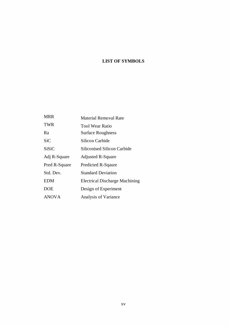
LIST OF SYMBOLS
MRR Material Removal Rate
TWR Tool Wear Ratio
Ra Surface Roughness
SiC Silicon Carbide
SiSiC Siliconised Silicon Carbide
Adj R-Square Adjusted R-Square
Pred R-Square Predicted R-Sqaure
Std. Dev. Standard Deviation
EDM Electrical Discharge Machining
DOE Design of Experiment
ANOVA Analysis of Variance
xvi
LIST OF APPENDIXES
APPENDIX TITLE PAGE
A Surface Roughness Out put 100
B Run Order Generated by design
Expert
113
C Scanning Electron Microscopy
Result
115
D Equipment 118

CHAPTER 1
INTRODUCTION
1.1 Introduction
In this age of technology and development, humans try to solve a lot of
problems and at the same time bring in many new materials. Silicon carbide ceramic
is one of the materials that has been invented especially for the automotive and
aerospace industry. It is an unusual material that is widely used in structural
applications because of its properties of excellent oxidation resistance, high
mechanical strength at elevated temperature, high hardness, high corrosion
resistance, high thermal conductivity and high thermal shock resistance impact due
to strong covalent Si-C bonds. But, because of the properties of this material, it
makes SiC difficult to be machined by conventional method. [1]

2
With the invention of Silicon Carbide, Electro Discharge Machining (EDM)
is playing an important role because it can remove material through erosion
regardless of the material hardness. This is due to the fact that no cutting force will
be induced during machining. Other than silicon carbide, any material that is
electrically conductive can be machined through this process. [1, 2]
This research is conducted to mainly evaluate the machining performance of
Silicon carbide using copper electrode which is a highly conductive and easy to
machine material. The majority of silicon carbide material types are expensive.
Because of that, proper planning on manufacturing is critical. Improper planning and
lack of machining data or suitable parameter setting will increase the waste of
material, time and finally increase the manufacturing cost. By this statement, it
shows that research in this area is really important to be performed. [3]
1.2 Problem Statement
EDM is a non-conventional machining technology that focuses on machining
of super hard conductive material. Because of this potential, it is extensively used
specially in the automotive and aerospace industries. Like conventional machining
operation, some suitable parameter settings need to be determined before conducting
the machining operation. It is to ensure that the machining process will be done in an
efficient and accurate manner. Every material that has different material properties
will have different suitability of parameter setting. For EDM operation, the
conductivity and melting temperature of material will play an important role. Many
other machining parameters will also influence its processing. Hence the best
3
solution to get a high machining efficiency is by developing appropriate
mathematical models for the specific material in hand. [4]
Diverse researches have been done on this machining process including the
selection of machining parameter for different materials in order to get best results.
But, until now the study is far from extensive. Although there is up-to-date data base
that comes together with the machine, it only covers for certain parameters and for
some material. Furthermore, the manufacturer’s guidelines for the selection of
machining parameters are traditional in nature and do not ensure finest and
economically efficient use of the machines. [3]
In EDM, the major challenge is to minimize the overcut and also to get the
maximum material removal rate (MRR) in regard to the best surface roughness (of
course when doing finishing job). [5]
Previous researches have been carried out on the machining of various types
of ceramic materials using EDM. However studies involving die sinking EDM
Siliconised Silicon Carbide (SiSiC) are few. As mentioned earlier, only electrically
conductive materials can be machined using this method. Silicon carbide that has
electrical resistance of more than 100 Ω cm will affect the EDM machining
efficiency. This study will be carrying out to investigate the relationship between the
certain parameters of machining and quality parameters of EDM process involving
SiSiC. [4, 6, 7]
4
1.3 Objective of the Research
The objectives of this study are:
(i) To identify the significant machining parameters and their effect on material
removal rate (MRR), surface roughness (Ra) and overall tool wear ratio
(TWR).
(ii) To identify the optimum setting for maximum material removal rate (MRR),
minimum surface roughness (Ra), minimum tool wear ratio (TWR)
Overall, the main objective of the project is to analyze the parameter settings of
EDM on SiSiC.
1.4 Scope of the Research
The scopes of this research are:
(i) The material that will be used is limited to reaction bonded silicon carbide
(RBSiC).
(ii) Discharge On-Time, Discharge Current, Off-Time and Tool polarity will
be studied as machining parameters.
(iii) Material Removal Rate, Tool Wear Ratio and Surface Roughness will be
studied as Quality Parameters.
(iv) Copper electrode will be employed.
(v) DOE will be used in this study.

5
1.5 Research Question
The research questions for this study are:
(i) What are the parameter settings that significant on the material removal rate
(MRR), tool wear ratio (TWR), and surface roughness (Ra)?
(ii) What is the relationship of every significant parameter on material removal
rate (MRR), tool wear ratio (TWR), and surface roughness (Ra)?
(iii) How the material removal rate (MRR), tool wear ratio (TWR), and surface
roughness (Ra) will be varied with varying of significant parameter setting?
(iv) What is the optimum setting for material removal rate (MRR), tool wear ratio
(TWR) and surface roughness (Ra)?
1.6 Significance of the Study
The research finding will give information on the factors that will contribute
to the studied responses namely material removal rate (MRR), tool wear ratio
(TWR), and surface roughness (Ra). Since there is still a lack of information on
EDM of conductive ceramic until now, the information will be beneficial for
potential users including those in the aerospace and automotive industries. The
information on the machining parameters will provide useful reference for better
efficiency of silicon carbide machining process.
96
Reference
[1] El-Hofy, Hassan. Advanced Machining Processes. McGraw Hill, 2005.
[2] Jain, V.K. Advanced (Non-traditional) Machining Processes.
[3] (2012). Chapter 3 - The Current Situation in Ultra-Precision Technology –
Silicon Single Crystals as an Example. Advances in CMP Polishing
Technologies. D. Toshiro, D. M. Ioan, I. D. M. Syuhei KurokawaA2 -
Toshiro Doi and K. Syuhei. Oxford, William Andrew Publishing: 15-111.
[4] Jahan, M. P., M. Rahman, et al. (2011). "A review on the conventional and
micro-electrodischarge machining of tungsten carbide." International Journal
of Machine Tools and Manufacture 51(12): 837-858.
[5] König, W., D. F. Dauw, et al. (1988). "EDM-Future Steps towards the
Machining of Ceramics." CIRP Annals - Manufacturing Technology 37(2):
623-631.
[6] Ji, R., Y. Liu, et al. (2011). "Experimental research on machining
characteristics of SiC ceramic with end electric discharge milling." Journal of
Mechanical Science and Technology 25(6): 1535-1542.
[7] Liu, Y., R. Ji, et al. (2008). "Electric discharge milling of silicon carbide
ceramic with high electrical resistivity." International Journal of Machine
Tools and Manufacture 48(12–13): 1504-1508.
[8] Kiyak, M. and O. Çakır (2007). "Examination of machining parameters on
surface roughness in EDM of tool steel." Journal of Materials Processing
Technology 191(1–3): 141-144.
97
[9] Mahardika, M., T. Tsujimoto, et al. (2008). "A new approach on the
determination of ease of machining by EDM processes." International Journal
of Machine Tools and Manufacture 48(7–8): 746-760.
[10] Mohd Abbas, N., D. G. Solomon, et al. (2007). "A review on current research
trends in electrical discharge machining (EDM)." International Journal of
Machine Tools and Manufacture 47(7–8): 1214-1228.
[11] http://www.vulcanmold.com.
[12] Matoorian, P., S. Sulaiman, et al. (2008). "An experimental study for
optimization of electrical discharge turning (EDT) process." Journal of
Materials Processing Technology 204(1–3): 350-356.
[13] NorlianaMohdAbbas, D. S., Md.FuadBahari (2006). "A review on current
research trends in electrical discharge machining." Machine Tools and
manufacture.
[14] Schumacher, B. M. (2004). "After 60 years of EDM the discharge process
remains still disputed." Journal of Materials Processing Technology 149(1–
3): 376-381.
[15] R.Venkataraman. "Multi Objective Optimization of Electro Discharge
Machining of Resin Bonded Silicon Carbide." Applied Mechanics and
Materials, 2012: 1556-1560.
[16] Tani, T., Y. Fukuzawa, et al. (2004). "Machining phenomena in WEDM of
insulating ceramics." Journal of Materials Processing Technology 149(1–3):
124-128.
98
[17] Luis, C. J., I. Puertas, et al. (2005). "Material removal rate and electrode wear
study on the EDM of silicon carbide." Journal of Materials Processing
Technology 164–165(0): 889-896.
[18] Leão, F. N. and I. R. Pashby (2004). "A review on the use of
environmentally-friendly dielectric fluids in electrical discharge machining."
Journal of Materials Processing Technology 149(1–3): 341-346.
[19] Tsai, Y. Y., C. H. Tseng, et al. (2008). "Development of a combined
machining method using electrorheological fluids for EDM." Journal of
Materials Processing Technology 201(1–3): 565-569.
[20] Puertas, I., C. J. Luis, et al. (2005). "Spacing roughness parameters study on
the EDM of silicon carbide." Journal of Materials Processing Technology
164–165(0): 1590-1596.
[21] Yonghong, L., J. Zhixin, et al. (1997). "Study on hole machining of non-
conducting ceramics by gas-filled electrodischarge and electrochemical
compound machining." Journal of Materials Processing Technology 69(1–3):
198-202.
[22] Chen, P.-Y., J. McKittrick, et al. "Biological materials: Functional
adaptations and bioinspired designs." Progress in Materials Science (2000).
[23] Puertas, I. and C. J. Luis (2004). "A study on the electrical discharge
machining of conductive ceramics." Journal of Materials Processing
Technology 153–154(0): 1033-1038.
[24] Baker, A. R., D. J. Dawson, et al. (1987). "Ceramics and composite materials
for precision engine components." Materials & Design 8(6): 315-323.
99
[25] Orlova, T. S., V. V. Popov, et al. (2011). "Electrical properties of biomorphic
SiC ceramics and SiC/Si composites fabricated from medium density
fiberboard." Journal of the European Ceramic Society 31(7): 1317-1323.
[26] Lenk, Reinhard, Aniko Nagy, Hans-Jurgen Richter, and Anja Techel.
"Material development for laser sintering technique." 2006.
[27] Ji, Renjie, Yonghong Liu, Yanzhen Zhang, Baoping Cai, Jianmin Ma, and
Hang Li. "Optimizing machining parameters of silicon carbide ceramics with
ED milling and mechanical grinding combined process." Int J Adv Manuf
Technol, 2010: 195–204.
[28] Montgomery, D.C. Design and Analysis of Experiments. 7th edition. John
Wiley & Sons, Inc. New York.
[29] Antony, J. (2003). 8 - Some useful and practical tips for making your
industrial experiments successful. Design of Experiments for Engineers and
Scientists. Oxford, Butterworth-Heinemann: 93-104.