(ELEC 5240 and ELEC 6240) Hardware Implementations
21
1 NEURAL NETWORKS (ELEC 5240 and ELEC 6240) Hardware Implementations Bodgan M. Wilamowski 2 Block diagram of an arbitrary nonlinear dynamic system. dt t x ) ( dt t x ) ( nonlinear terms dt t x ) ( nonlinear terms nonlinear terms 1 x 2 x n x 1 y 2 y n y dt y y y x x x f y dt y y y x x x f y dt y y y x x x f y n n n n n n n n , , , , , , , , , , , , , , , 2 1 2 1 2 1 2 1 2 2 2 1 2 1 1 1 Introduction
Transcript of (ELEC 5240 and ELEC 6240) Hardware Implementations

1
NEURAL NETWORKS (ELEC 5240 and ELEC 6240)
Hardware Implementations
Bodgan M. Wilamowski
2Block diagram of an arbitrary nonlinear dynamic system.
dttx )(
dttx )(
nonlinearterms dttx )(
nonlinearterms
nonlinearterms1x
2x
nx
1y
2y
ny
dtyyyxxxfy
dtyyyxxxfy
dtyyyxxxfy
nnnn
nn
nn
,,,,,
,,,,,
,,,,,
2121
212122
212111
Introduction

3
How to implement nonlinear terms?
dttx )(
dttx )(
nonlinearterms dttx )(
nonlinearterms
nonlinearterms1x
2x
nx
1y
2y
ny
1x
2x
nx
1y
2y
ny
How to handle nonlinear systems?
dttx )(
How to implement nonlinear terms?
easypart
4Block diagram of an arbitrary linear dynamic systemusing transconductance amplifiers.
dtyyyxxxfy
dtyyyxxxfy
dtyyyxxxfy
nnnn
nn
nn
,,,,,
,,,,,
,,,,,
2121
212122
212111
Implementations of Dynamic Linear Systems
state variables(functions are linear)
1x
2x
nx
1y
2y
ny

5Transconductance amplifier with a multiple inputs. Gains are adjusted by
digitally controlled biasing currents IA and IB
Implementations of Dynamic Linear Systems 1x
2x
nx
1y
2y
ny
AV1 AV2
BBMAAAMAOUT VVgVVgi 2121
BV1
BV2
BV2
AV1
BV1
AV2OUTi
AI BI
6Circuit with a digitally programmable current gain with 6 bit accuracy
Digitally adjusted analog circuits
AV1 AV2
BBMAAAMAOUT VVgVVgi 2121
BV1
BV2
BV2
AV1
BV1
AV2OUTi
AI BI
1 2 4
1 2 4
14
4 1
2
1
1 2 4
8 16 32
W/L are mareked
Outputcurrent
Inputcurrent
M1 M2
M3
M10M5
M6 M9M8M7
M4
M13 M15
M16 M17 M18
M14
M11 M12
B0 B1 B2
B5B3 B4
Please notice effective use of the chip space since the maximum ratio in the transistor size is only four

7
Fifth order low-pass Chebyshev filter transconductance filter using ladder prototype. Transcounductance amplifiers are digitally adjusted to obtain proper characteristics
Implementations of fifth order Chebyshev filter
AV1 AV2
BBMAAAMAOUT VVgVVgi 2121
BV1
BV2
BV2
AV1
BV1
AV2OUTi
AI BI
+-
I1 I5
V2 V4Vin
RinsL 1
13
1
sL4
1
sCRoutsL 5
1Mg Mg
MgMg Mg
I3
3
1
sC
L1 L3L4
C2 C4
Rin Rout
+-
Rin
Rout
L1
C2
L3
C4
L5
8
Implementations of fifth order Chebyshev filter
Frequency
10Hz 100Hz 1.0kHz0V
200mV
400mV
600mV
800mV
+-
I1 I5
V2 V4Vin
RinsL 1
1
3
1
sL 4
1
sC RoutsL 5
1
Mg MgMgMg Mg
I3
3
1
sC
C CC
C
R R
C
L1 L3 L5C2 C4
Characteristic of the system are digitally adjusted to obtain proper
characteristics
The question: How to handle nonlinear systems?
Any dynamic linear system can be implemented on VLSI chip
this way
Gm’s of transcounductance amplifiers are adjusted digitally

9
Control surfaces obtained with Motorola microcontroller HC11 using fuzzy
approach with trapezoidal membership functions (7 functions per input) and
Tagagi-Sugeno defuzzification
Fuz
zifie
r
X
Y
out
Def
uzzi
ficat
ion
Fuz
zifie
r
Rule selection cellsmin-max operations Fuzzy Systems
10
Control surfaces obtained with Motorola microcontroller HC11 using fuzzy
approach with six neurons 2-1-1-1-1-1 architecture and Elliot activation function
out
Neural Networks

11
Fuzzy systems VLSI implementation
Block diagrams of the fuzzy VLSI chip
fuzz
yfie
rs
64 M
INop
erat
ors
8+8(fuzzy)
64(fuzzy)
2 inputs(analog)
1 output(analog)
wei
ghte
dsu
m
norm
aliz
ario
n
64(fuzzy)
Control surfaces: (a) desired control surface, (b) information stored in defuzzifier as weights, and (c) measured control surface of VLSI chip
Fuz
zyfie
rF
uzzy
fier
X
Y
Array ofcluster cells
out
weightedcurrents
voltages
12
Fuzzy systems VLSI implementation 2
refe
ren
ce
vo
lta
ge
s
fuzzy current variables
VIN
I1 I2 I3 I4 I5 I6
(a)
0 1 2 3 40
1
2
3
4
5
6
7
8
9
10
VIN
Cur
rent
s[u
A]
I1 I2 I3
Fuzzyfier with Six Diffrent Membership
Fuzzifier (a) circuit diagram of fuzzifier, (b) example of the SPICE simulation

13
Fuzzy systems VLSI implementation 3
outp
ut to
sum
min
g no
de
W/LW/L W/L
fuzz
y in
puts
Defuzzifier using normalization and weighted sum
MIN
(A,B
)
A
B
(a) (b)
IA
IB
ITH IBIAS
VREF
VDD
IOUT
Selection circuits (a) MIN circuit in voltage mode (b) neuron circuit with
threshold in the current mode
14
Fuzzy systems VLSI implementation 4
MAX operators (a) concept diagram and (b) simulation results for MAX1 and for the proposed MAX2.
M1
+VDD
I1 I2
IMAX
IBIAS
M3M2
M4 M51 2
3
VBIAS6 7 8
5M6 M7 M8
0 0.5 1 1.5 2 2.5 3 3.5 49
9.2
9.4
9.6
9.8
10
10.2
10.4
10.6
10.8
11
I1
I2
MAX2MAX1
Comparison of MAX circuits
TIME
Cur
rent
s
[s]
[uA
]

15
Fuzzy systems VLSI implementation 5
The cluster cell with rule selection (transistors M1-M4) and defuzzification (source I0 and
transistors M4-M6)
Six bit programmable current sources
X i-th fuzzy voltage
Z k-th fuzzy voltage
Y j-th fuzzy voltage
to globalsumming node
common nodesupplied by singleconstant current
source
W/L sets the outputvalue for the cluster
+12V
I0
M1 M2 M3
M4
M5 M6
1 2 4
1 2 4
IREF
14
4 1
2
1
1 2 4
8 16 32
W/L are marked
16
Fuzzy systems VLSI implementation 6
Normalization circuit (a) circuit diagram and (b) characteristics
I1 I3
1
M1 M2 M3 M4
+-
IBIASVREF
M5 M6
I2
78
IN1 IN3IN2
2 3
0 0.05 0.10
0.02
0.04
0.06
0.08
0.1
0.12
0.14
0.16
0.18
0.2
I2
Normalization Circuit
I1
Cur
rent
s[u
A]

17Microphotograph of the analog fuzzy .
18
Sigmoidal function generated by differential pair
M2
M3 M4VIN
M1
IREFVX
IM3 IM4
IM2
VLSI implementations of Neural Networks
-1 -0.8 -0.6 -0.4 -0.2 0 0.2 0.4 0.6 0.8 1
L
W
L
W
ou
tpu
t cu
rre
nts
input voltage
negativeoutput
positiveoutput
20
15
10
5
0
-15
-10
-5
[A
]
[V]

19
Weight circuits
VLSI implementations of Neural Networks
Mb
M5Ma
+VDD
Mb
Ma
Mb
Ma
Mb
Ma
IREF
M1
IM3
20The neuron circuit with voltage type input and weighted current outputs
VLSI implementations of Neural Networks
M2 Md
M3 M4
M5 M6Mc
+OUT -OUT
+VDD
IN
Mb
Ma
Mb
Ma
Mb
Ma
Mb
Ma
Md
Mc
M1
IREF
Md
Mc
Md
Mc
biasbias

21
Circuit for current to voltage conversion
VLSI implementations of Neural Networks
IIN
+VDD
M11
M12 VIN
+
-
+-
VREF
RIN
VIN
+
-
IIN
22
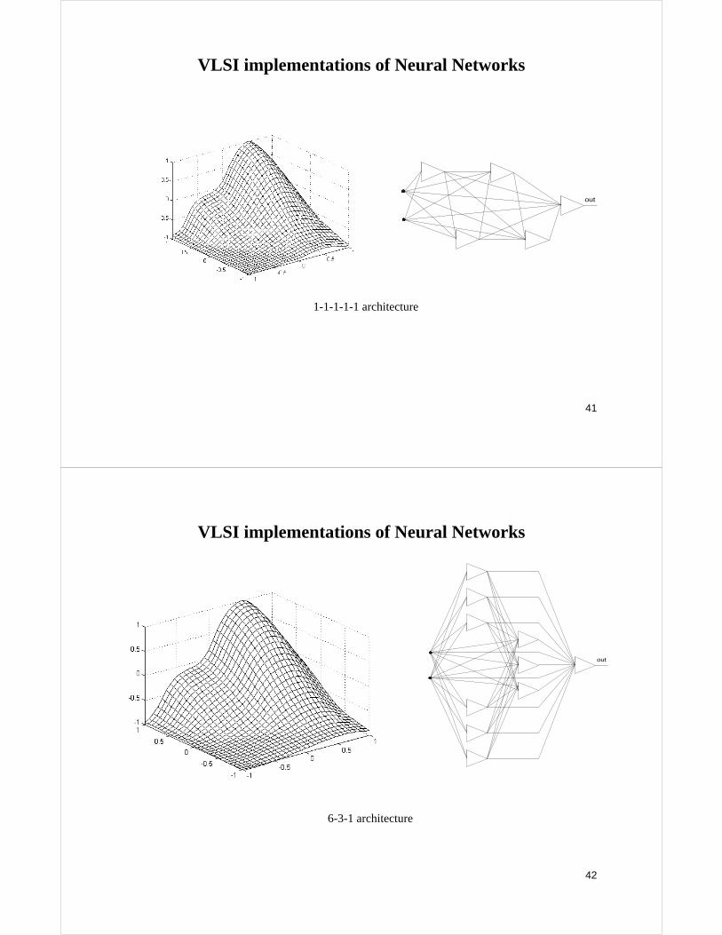
1-1-1-1-1 architecture
VLSI implementations of Neural Networks
out

23
6-3-1 architecture
VLSI implementations of Neural Networks
out
24
Required control surface
VLSI implementations of Neural Networks
Neural network architectures Error
No. Layers No. Weights Architecture (SSE )
3 9 1 1 1 1.207
4 14 1 1 1 1 0.2336
5 20 1 1 1 1 1 0.07
3 18 2 2 1 1.6268
2 17 5 1 0.8713
3 29 3 3 1 0.4844
3 49 5 4 1 0.0843
3 47 6 3 1 0.0312
4 53 4 4 1 1 0.0173
4 55 4 3 2 1 0.0525
2 32 10 1 0.1258

25
VLSI nonlinear signal processing
Piece-wise function synthesis
IIN IOUT
I2I1
IIN
IOUT
I2
I1
c
1
2
W
W
IIN IOUT
I1 I2
IIN
IOUT
I2
I1
1
2
W
W
M1 M2 M4M3
I1IIN
IOUT
1I
I2
26
VLSI nonlinear signal processing
Piece-wise function synthesis
1
2 3 5
6 7 9
10
11
12
99
M1M2 M3 M4 M5
M21 M31 M41 M42
M11M23 M33 M43
M22 M32Ibias
IIN
M34 M35M8 M7
IOUT

27
VLSI nonlinear signal processing
Low voltage (<1V) piece-wise function synthesis
M1 M2
M4M3
IIN
M6M7
IOUT
28
VLSI nonlinear signal processing
Absolute value operator
ABS( )
M2M1
M5 M6
VREF
VREF
IN
Iin
-10uA -5uA 0A 5uA 10uAID(M8a)
0A
4uA
8uA
12uA

29
VLSI nonlinear signal processing
Analog to Gray Code converter Iin
-10uA -8uA -6uA -4uA -2uA 0uA 2uA 4uA 6uA 8uA 10uAI(xabs1:1) I(xabs2:1) I(xabs3:1) I(xabs4:1) I(xabs5:1) I(xabs6:1) I(xabs7:1) I(xabs8:1)
-10uA
0A
10uA
V(21) V(22)+6 V(23)+12 V(24)+18 V(25)+24 V(26)+30 V(27)+36 V(28)+42
SEL>>
30
VLSI nonlinear signal processing
Voltage mode MAX operator
out
M1
+VDD
I1 I2
IMAX
IBIAS
M3M2
M4 M51 2
3
Current mode MAX operator

31
VLSI nonlinear signal processing
I2
IMIN
I1
M1M2
M3 M4
M5
I2IMIN
I1
M1M2
M3 M4
M5
M6
M7VREF
VB
6
4
2
1
5
3
7
8
1 2 3
VBM88
Current mode MIN (a) concept (b) implementation
32
VLSI nonlinear signal processing
Current to current sigmoidal type activation function
I0
M1 M2
M3 M4
I0
M5 M6
M7 M8
IIN IOUTVREF1
VREF2

33
VLSI nonlinear signal processing
M1 M2
M3 M4
M5 M6
M7 M8
VREF1
VREF3
VREF2
OUT
ISS
0.5ISS
0 1 2 3 4 5-6
-4
-2
0
2
4
6
ou
tpu
t cu
rre
nt
input voltage [V]
[uA
]
(a) (b)Circuit performing sin and cos operations (a) circuit diagram and (b) result
of Spice simulation
34
VLSI nonlinear signal processing
(a) (b)Circuit diagram of multiplier/divider (a) concept diagram and (b) actual
implementation.
I1I3
I2
3
21
I
III M1
M2
M3
VDD
1
2
3
VDDVDD
M4
I1 I3
I2
3
21
I
III
M1
M2
M3
VDD
1
2 3
VDDVDD
M4
M5
M6
M7
4
6
5
7
M8
8
M9

35
VLSI nonlinear signal processing
(a) (b)The circuit as (a) signal multiplier and (b) signal divider.
10 20 30 40 50 60 70 80 900
20
40
60
80
100
120
140
I1
I2
I3
Iout
Multiplier
I1
Cur
rent
s
[nA]
[nA
]
0 20 40 600
20
40
60
80
100
120
140
I1
I2
I3
Divider
I1
Cur
rent
s [n
A]
36
VLSI nonlinear signal processing
Circuit diagram of four-quadrant multiplier
0
21
I
iiIOUT
I0
M1
M2
M3
VDD
1
2 3
VDD
M4
M5
M6
M7
4
6
5
7
M8
8
M9
I0
I0I0
i1
i2
9
i1
i2
0 0.5 1 1.5-50
-40
-30
-20
-10
0
10
20
30
40
50
OUT
IN
Four-quadrant multiplier as the
TIME
Cur
rent
s[n
A]
Multiplier used as the frequency doubler.
0
21
I
iiIOUT

37
Bipolar versus unipolar neurons
unipolarbipolar made
of unipolar
-1
+1
+2
bipolarunipolar made
of bipolar
0.5
+1
+0.5
unipolar
bipolar
38
Microprocessor Implementation of Neural Networks
Required control surface
6 neurons in one hidden layer6 neurons in cascade
4 neurons in cascade

39
Comparison of various fuzzy and neural controllers
Type of controller length of code
processing time (ms)
Error MSE
Zadeh with trapezoidal 2324 1.95 0.945
Zadeh with triangular 2324 1.95 0.671
Zadeh with Gaussian 3245 39.8 0.585
Tagagi-Sugeno with trapezoidal 1502 28.5 0.309
Tagagi-Sugeno with triangulal 1502 28.5 0.219
Tagagi-Sugeno with Gaussian 2845 52.3 0.306
Neural network with 3 neurons in cascade
680 1.72 0.00057
Neural network with 5 neurons in cascade
1070 3.3 0.00009
Neural network with 6 neurons in one hidden layer
660 3.8 0.00030
40
Neural systems -microprocessor implementation
Required control surface
41
1-1-1-1-1 architecture
VLSI implementations of Neural Networks
out
42
6-3-1 architecture
VLSI implementations of Neural Networks
out