Eindhoven University of Technology MASTER Distortion ... · The final channel selection is done in...
58
Eindhoven University of Technology MASTER Distortion analysis of differential amplifiers de Goey, L.P. Award date: 1995 Link to publication Disclaimer This document contains a student thesis (bachelor's or master's), as authored by a student at Eindhoven University of Technology. Student theses are made available in the TU/e repository upon obtaining the required degree. The grade received is not published on the document as presented in the repository. The required complexity or quality of research of student theses may vary by program, and the required minimum study period may vary in duration. General rights Copyright and moral rights for the publications made accessible in the public portal are retained by the authors and/or other copyright owners and it is a condition of accessing publications that users recognise and abide by the legal requirements associated with these rights. • Users may download and print one copy of any publication from the public portal for the purpose of private study or research. • You may not further distribute the material or use it for any profit-making activity or commercial gain
Transcript of Eindhoven University of Technology MASTER Distortion ... · The final channel selection is done in...
Eindhoven University of Technology
MASTER
Distortion analysis of differential amplifiers
de Goey, L.P.
Award date:1995
Link to publication
DisclaimerThis document contains a student thesis (bachelor's or master's), as authored by a student at Eindhoven University of Technology. Studenttheses are made available in the TU/e repository upon obtaining the required degree. The grade received is not published on the documentas presented in the repository. The required complexity or quality of research of student theses may vary by program, and the requiredminimum study period may vary in duration.
General rightsCopyright and moral rights for the publications made accessible in the public portal are retained by the authors and/or other copyright ownersand it is a condition of accessing publications that users recognise and abide by the legal requirements associated with these rights.
• Users may download and print one copy of any publication from the public portal for the purpose of private study or research. • You may not further distribute the material or use it for any profit-making activity or commercial gain
Eindhoven University of TechnologyFaculty of Electrical Engineering
Digital Systems Group (EB)
Distortion Analysis ofDifferential Amplifiers
L.P. de GoeyMay 1995
Report of the Graduation projectPerformed from October1994 to May 1995
at the Philips Research LaboratoriesEindhoven, The Netherlands.
Coach: Prof.dr.ir. R.J. van de Plassche
© Philips Electronics N. V. 1994All rights reserved. Reproduction in whole or in part is
prohibited without written consent of the copyright owner.
Eindhoven University of TechnologyFaculty of Electrical Engineering
Digital Systems Group (EB)
Distortion Analysis ofDifferential Amplifiers
L.P. de GoeyMay 1995
Report of the Graduation projectPerformed from October1994 to May 1995
at the Philips Research LaboratoriesEindhoven, The Netherlands.
Coach: Prof.dr.ir. R.J. van de Plassche
© Philips Electronics N.V. 1994All rights reserved. Reproduction in whole or in part is
prohibited without written consent of the copyright owner.
Abstract
In an attempt to create a digital receiver it became clear that an analog frontendwas necessary. This analog frontend should condition the antenna signal so thatan AD converter can be fed. A final part in this analog frontend is an amplifierthat amplifies the signal's amplitude to a level close to the full scale of the ADconverter.The specification for the analog frontend, and thus the fixed gain amplifier, aremainly determined by the choice of the analog to digital converter. A ten bits ADconverter implies a signal to noise ratio of -62 dB.Several principles of differential amplifiers implemented using bipolar transistors are discussed.In the first part the circuits are discussed theoretically. Here equations for thegain and the level of third order harmonic distortion are derived.In the second part a comparison of the theoretical behaviour with the results fromcomputer simulation is made. The simulation results show that the theoreticalanalysis can be used to do coarse calculations of the circuit, provided that allboundary conditions are met. Using the simulation results the circuits can be adjusted to maximum performance.A simple differential pair amplifier proved to get the best gain-distortion ratio,but lacked a low output impedance. Buffering a simple differential pair amplifierwith two emitter followers caused the gain to decrease.The transresistance amplifier caused as much third order distortion as was gainedby the increment of voltage space. At higher output signal amplitudes the transre·sistance amplifier seemed to get a better result.For the desired output signal amplitude of 1 Volt a distortion level of -65 dB isthe best result realized. While for a distortion level of ·80 dB an output signalamplitude of only 450 milliVolt could be achieved. Overall can be concluded thatthe level of third order harmonic distortion is mainly dependent on the amplitudeof the output signal.
© Philips Electronics N.V.
Contents
1 Introduction 1
2 Deriving The Specifications 3
2.1 Signal levels 3
2.2 Signal frequencies 4
3 Theory Of Operation 7
3.1
3.2
3.3
3.4
3.5
3.6
3.7
3.7.1
3.8
4
4.1
4.2
4.3
4.4
4.5
4.6
4.7
5
6
The Bipolar NPN Transistor 7
The Differential Pair 9
A Differential Pair Amplifier 12
A Differential Pair Amplifier With Feedback 14
The Emitter Follower Output Stage 19
The Differential Pair Amplifier With Output Stage 20
The Transresistance Amplifier 21
Implementing A Differential Pair Amplifier 22
A Three Stage Differential Amplifier 25
Implementation And Simulation 27
The Simulation Model Of The Bipolar NPN-Transistor 27
The Differential Pair Amplifier. 28
The Feedback Differential Pair Amplifier 31
The Emitter Follower Output Stage 34
Differential Pair Amplifier With Output Stage 36
The Transresistance Amplifier 38
The Three Stage Differential Amplifier 41
Conclusions And Recommendations 47
Acknowledgement 49
Appendix A Bibliography 51
Appendix B Distortion Calculus 53
Appendix C Cascading Stages 55
© Philips Electronics N.V.
1 Introduction
1 Introduction
Over the last years the application of digital techniques has made enormous steps forward.Even in traditionally analog systems digital components marched in. The main advantages ofthis takeover are increasing performance and a simple means of implementing new features.The increase in performance is a direct result of the lack of loss of performance throughoutthe digital system. This is caused by the discrete levels which are maintained throughout thesystem. The variation of the signal, in well designed digital systems, never results in a wronglevel. New features can easily be implemented because calculation with digital data can bedone very fast and this area of research is widely covered.
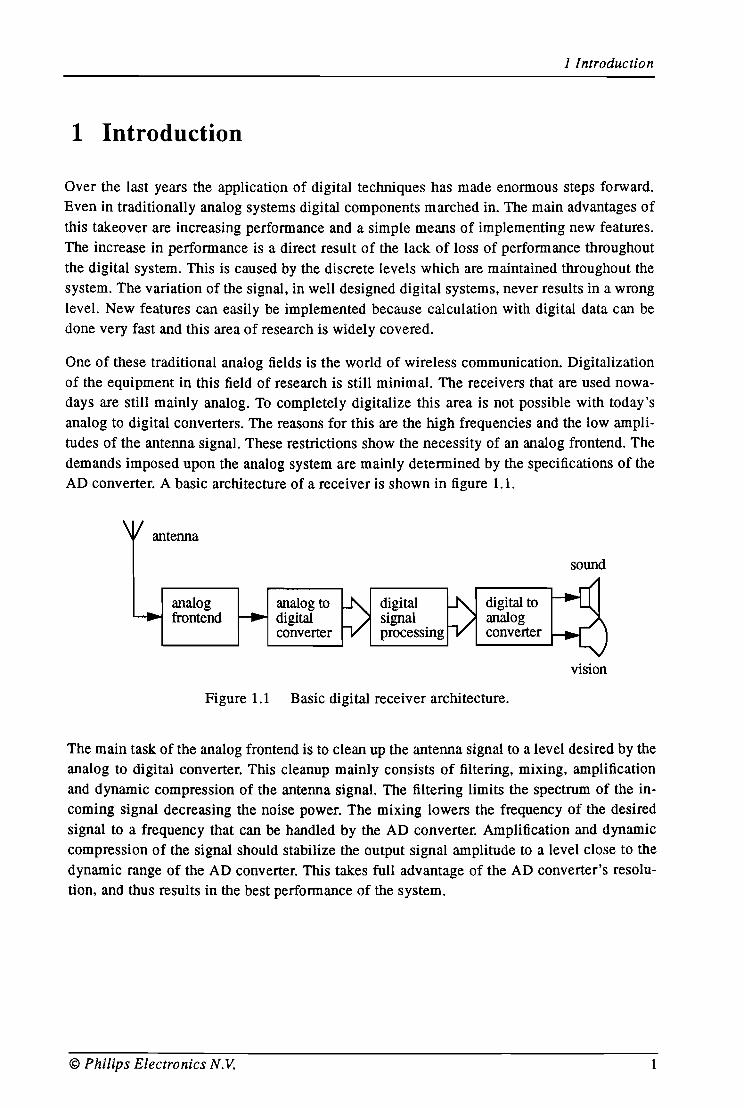
One of these traditional analog fields is the world of wireless communication. Digitalizationof the equipment in this field of research is still minimal. The receivers that are used nowadays are still mainly analog. To completely digitalize this area is not possible with today'sanalog to digital converters. The reasons for this are the high frequencies and the low amplitudes of the antenna signal. These restrictions show the necessity of an analog frontend. Thedemands imposed upon the analog system are mainly determined by the specifications of theAD converter. A basic architecture of a receiver is shown in figure 1.1.
antenna
sound
analogfrontend
analog todigitalconverter
digitalsignalprocessing
digital toanalogconverter
vision
Figure 1.1 Basic digital receiver architecture.
The main task of the analog frontend is to clean up the antenna signal to a level desired by theanalog to digital converter. This cleanup mainly consists of filtering, mixing, amplificationand dynamic compression of the antenna signal. The filtering limits the spectrum of the incoming signal decreasing the noise power. The mixing lowers the frequency of the desiredsignal to a frequency that can be handled by the AD converter. Amplification and dynamiccompression of the signal should stabilize the output signal amplitude to a level close to thedynamic range of the AD converter. This takes full advantage of the AD converter's resolution, and thus results in the best performance of the system.
© Philips Electronics N.V. 1
Ilntroduction
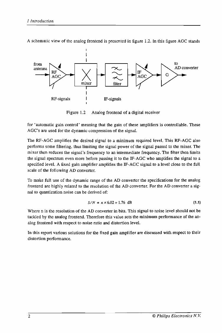
A schematic view of the analog frontend is presented in figure 1.2. In this figure AGC stands
fromantenna
Xmixer
"X....,
"~filter
toAD converter
RF-signals IF-signals
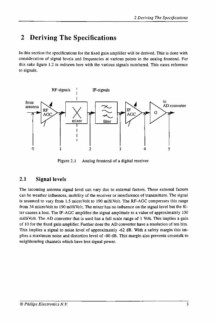
Figure 1.2 Analog frontend of a digital receiver
for 'automatic gain control' meaning that the gain of these amplifiers is controllable. TheseAGC's are used for the dynamic compression of the signal.
The RF-AGC amplifies the desired signal to a minimum required level. This RF-AGC alsoperforms some filtering, thus limiting the signal power of the signal passed to the mixer. Themixer then reduces the signal's frequency to an intermediate frequency. The filter then limitsthe signal spectrum even more before passing it to the IF-AGC who amplifies the signal to aspecified level. A fixed gain amplifier amplifies the IF-AGC signal to a level close to the fullscale of the following AD converter.
To make full use of the dynamic range of the AD converter the specifications for the analogfrontend are highly related to the resolution of the AD converter. For the AD converter a signal to quantization noise can be derived of:
SIN = n x 6.02 + 1.76 dB (1.1)
Where n is the resolution of the AD converter in bits. This signal to noise level should not betackled by the analog frontend. Therefore this value sets the minimum performance of the analog frontend with respect to noise ratio and distortion level.
In this report various solutions for the fixed gain amplifier are discussed with respect to theirdistortion performance.
2 © Philips Electronics N. V.
2 Deriving The Specifications
2 Deriving The Specifications
In this section the specifications for the fixed gain amplifier will be derived. This is done withconsideration of signal levels and frequencies at various points in the analog frontend. For
this sake figure 1.2 is redrawn here with the various signals numbered. This eases referenceto signals.
o
RF-signals
1
Xmixer
2
IF-signals
--x"""~
filter
3 4
toAD converter
5
Figure 2.1 Analog frontend of a digital receiver
2.1 Signal levels
The incoming antenna signal level can vary due to external factors. These external factorscan be weather influences, mobility of the receiver or interference of transmitters. The signalis assumed to vary from 1.5 microVolt to 190 milliVolt. The RF-AGC compresses this range
from 34 microVolt to 190 milliVolt. The mixer has no influence on the signal level but the filter causes a loss. The IF-AGe amplifies the signal amplitude to a value of approximately 100
milliVolt. The AD converter that is used has a full scale range of 1 Volt. This implies a gainof 10 for the fixed gain amplifier. Further does the AD converter have a resolution of ten bits.This implies a signal to noise level of approximately -62 dB. With a safety margin this implies a maximum noise and distortion level of -80 dB. This margin also prevents crosstalk to
neighbouring channels which have less signal power.
© Philips Electronics N.V. 3
2 Deriving The Specifications
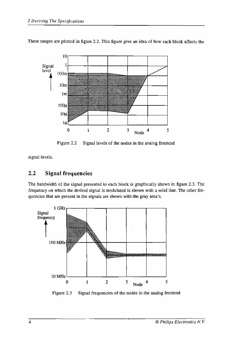
These ranges are plotted in figure 2.2. This figure give an idea of how each block affects the
10
Signal 1level
110m
1m
100/-1
10/-1 .
1/-1
0 1 2 3Node
4 5
Figure 2.2 Signal levels of the nodes in the analog frontend
signal levels.
2.2 Signal frequencies
The bandwidth of the signal presented to each block is graphically shown in figure 2.3. Thefrequency on which the desired signal is modulated is shown with a solid line. The other frequencies that are present in the signals are shown with the gray area's.
1 GHzr----~------,----r---___r--____,
54Node
321
10 MHz '--__---L....__----I ....L-__---l.__-'
o
100 MHz
Figure 2.3 Signal frequencies of the nodes in the analog frontend
4 © Philips Electronics N.V.
2 Deriving The Specifications
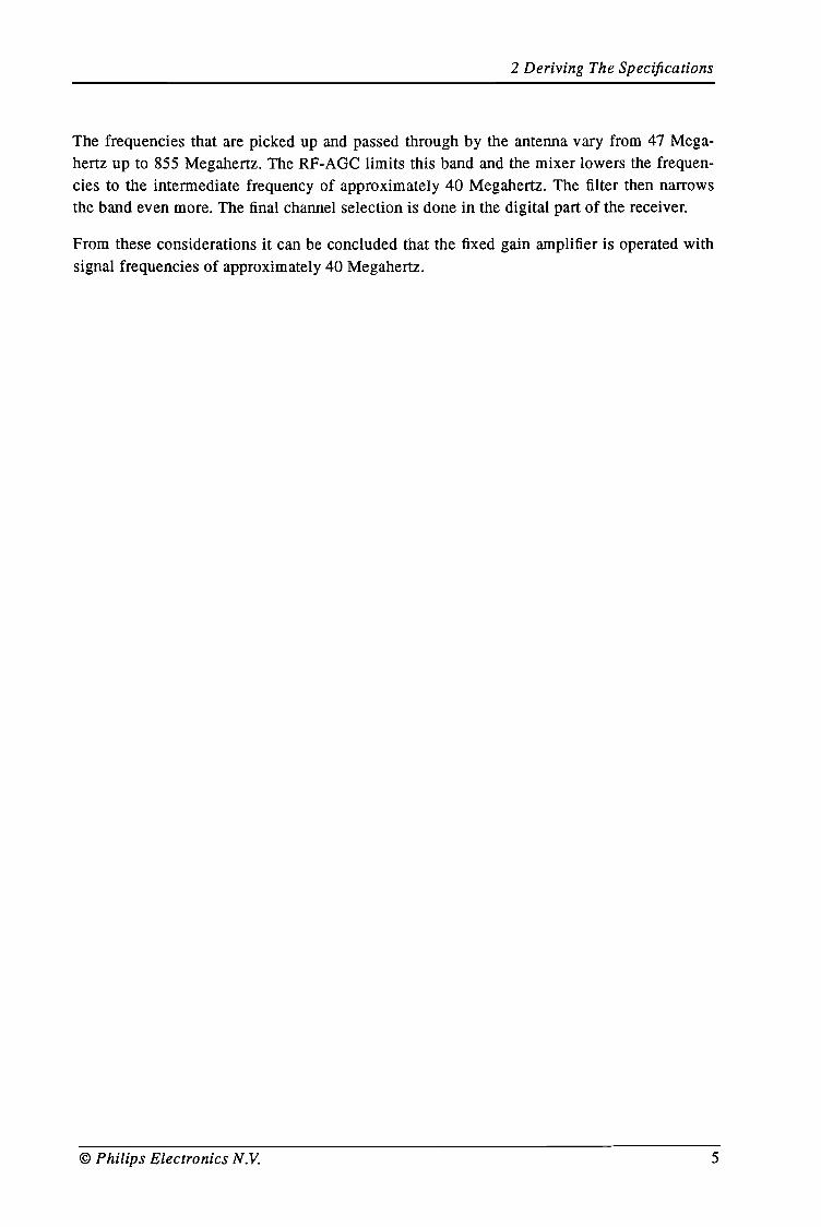
The frequencies that are picked up and passed through by the antenna vary from 47 Megahertz up to 855 Megahertz. The RF-AGC limits this band and the mixer lowers the frequencies to the intermediate frequency of approximately 40 Megahertz. The filter then narrowsthe band even more. The final channel selection is done in the digital part of the receiver.
From these considerations it can be concluded that the fixed gain amplifier is operated withsignal frequencies of approximately 40 Megahertz.
© Philips Electronics N.V. 5
3 Theory Of Operation
3 Theory Of Operation
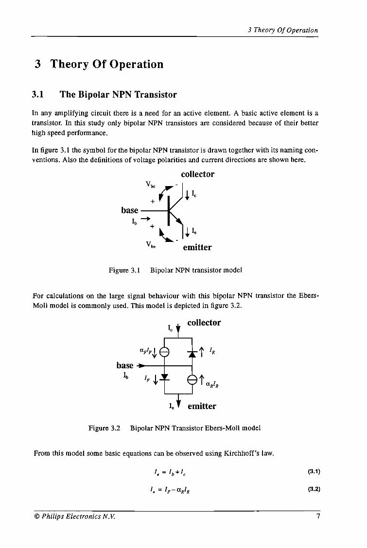
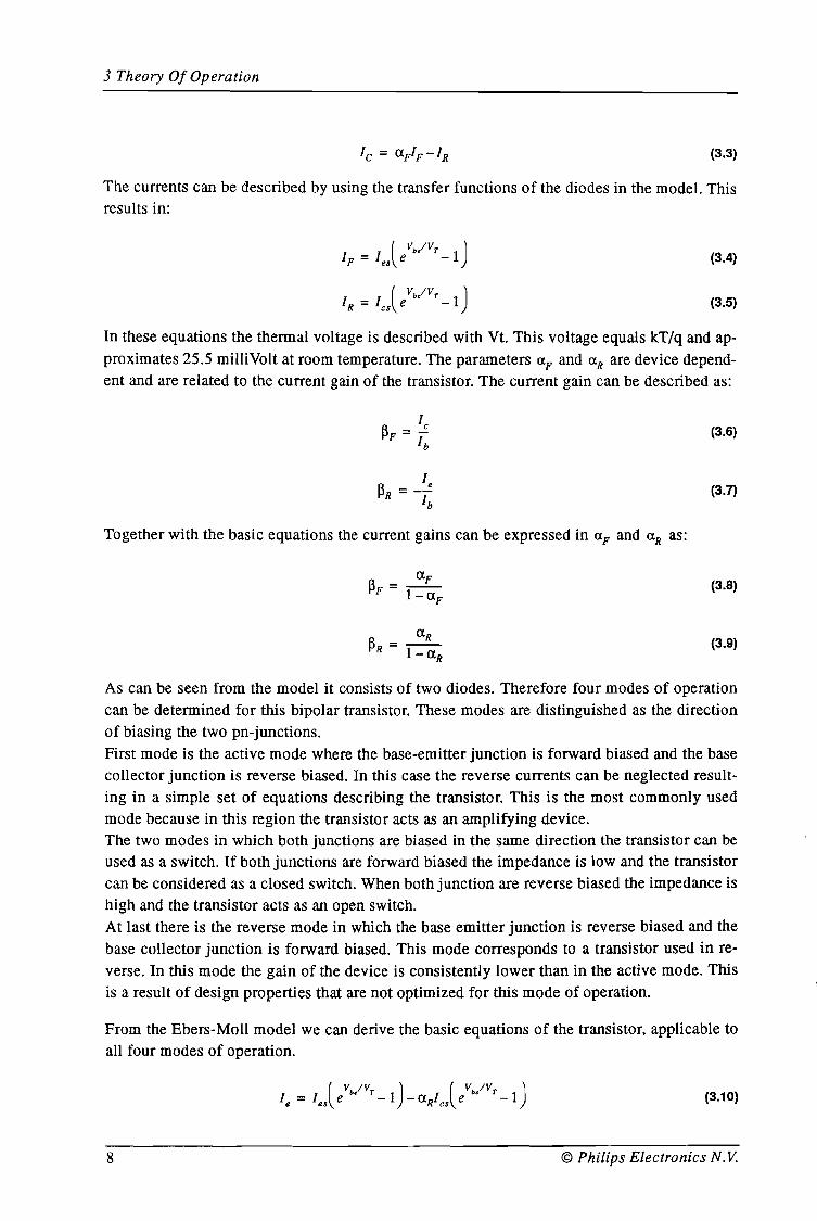
3.1 The Bipolar NPN Transistor
In any amplifying circuit there is a need for an active element. A basic active element is atransistor. In this study only bipolar NPN transistors are considered because of their betterhigh speed performance.
In figure 3.1 the symbol for the bipolar NPN transistor is drawn together with its naming conventions. Also the definitions of voltage polarities and current directions are shown here.
collector
base ----I[
1-'
b + ~_ p.Vbe emitter
Figure 3.1 Bipolar NPN transistor model
For calculations on the large signal behaviour with this bipolar NPN transistor the EbersMoll model is commonly used. This model is depicted in figure 3.2.
collector
(lFIF{, t IR
baseIb IF {, t (lRIR
emitter
Figure 3.2 Bipolar NPN Transistor Ebers-Moll model
From this model some basic equations can be observed using Kirchhoff's law.
© Philips Electronics N.V.
(3.1)
(3.2)
7
3 Theory Of Operation
(3.3)
The currents can be described by using the transfer functions of the diodes in the model. Thisresults in:
(3.4)
(3.5)
In these equations the thermal voltage is described with Vt. This voltage equals kT/q and ap
proximates 25.5 milliVolt at room temperature. The parameters rJ.F and rJ.R are device dependent and are related to the current gain of the transistor. The current gain can be described as:
(3.6)
(3.7)
Together with the basic equations the current gains can be expressed in rJ.F and rJ.R as:
(3.8)
(3.9)
As can be seen from the model it consists of two diodes. Therefore four modes of operationcan be determined for this bipolar transistor. These modes are distinguished as the directionof biasing the two pn-junctions.
First mode is the active mode where the base-emitter junction is forward biased and the basecollector junction is reverse biased. In this case the reverse currents can be neglected resulting in a simple set of equations describing the transistor. This is the most commonly usedmode because in this region the transistor acts as an amplifying device.The two modes in which both junctions are biased in the same direction the transistor can beused as a switch. If both junctions are forward biased the impedance is low and the transistorcan be considered as a closed switch. When both junction are reverse biased the impedance ishigh and the transistor acts as an open switch.At last there is the reverse mode in which the base emitter junction is reverse biased and thebase collector junction is forward biased. This mode corresponds to a transistor used in reverse. In this mode the gain of the device is consistently lower than in the active mode. Thisis a result of design properties that are not optimized for this mode of operation.
From the Ebers-Moll model we can derive the basic equations of the transistor, applicable toall four modes of operation.
8
(3.10)
© Philips Electronics N. V.
3 Theory Of Operation
(3.11)
Because here the transistors are only used as an amplifying device, we can simplify theseequations. First the reverse currents are neglected. This is valid if the base collector junctionis reverse biased. In the active mode the base emitter junction is forward biased so the leakage current can be neglected with respect to the collector current. With these simplificationswe get:
(3.12)
(3.13)
For the validity of these equation the following conditions are to be met:
Vbe > O.7Volt
(3.14)
(3.15)
These simple equations applicable to the active mode of the transistor are used in further calculations in this report.
3.2 The Differential Pair
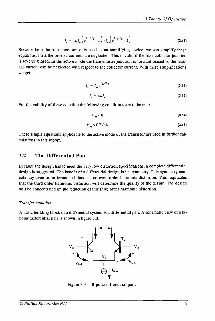
Because the design has to meet the very low distortion specifications, a complete differentialdesign is suggested. The benefit of a differential design is its symmetry. This symmetry cancels any even order terms and thus has no even order harmonic distortion. This implicatesthat the third order harmonic distortion will determine the quality of the design. The designwill be concentrated on the reduction of this third order harmonic distortion.
Transfer equation
A basic building block of a differential system is a differential pair. A schematic view of a bipolar differential pair is shown in figure 3.3.
Figure 3.3 Bipolar differential pair.
© Philips Electronics N.V. 9
3 Theory Of Operation
The differential pair basically acts as a current distributor. The currents flowing through thecollector of the transistors is dependent on the voltage difference between the base contacts.If there is no voltage applied, that is Vip=Vin, the currents that flow through the transistorswill be equal. As Vip is increased and V in is decreased in the same way, leI will increase andIc2 will decrease in the same order.
Now the transfer function of the bipolar differential pair will be derived using the transistordesign model equations (3.12) and (3.13) for the active mode as described in section 3.1
First the input and output signals are defined as:
Vip = Vern + V/2
V in = V ern - V/2
Ie! = f1.Flbia/2+lo
le2 = f1.Fl bia/2 -10
(3.16)
In these definitions the input voltages and output currents are split in their differential andquiescent terms. With equations (3.12) and (3.13) the collector currents can be related with
the input voltages.
With the definitions in equation (3.16) the output current 10can be expressed as:
Ie! -le2/0 = 2
les( (Vip-Vo)/Vr (Vin-Vo)/Vr )= "2 e -e
/es( (Vcm- VO+ Vi/2)/Vr (Vcm- Vo- V/ 2)/Vr )= 2" e -e
les (Vcm-Vo)/Vr( Vi/2Vr V/2Vr)= "2e e-e
By considering the quiescent currents an expression for the first term can be found:
Rewriting this expression leads to:
(3.17)
(3.18)
(3.19)
(3.20)
(3.21)
10 © Philips Electronics N.V.
(3.22)
3 Theory Of Operation
Substitution in equation (3.19) results in:
Vil2VT V/2VT )
I = uFIbias e - eo V/2VT VI/2VT
2 e + e
uFlb · V.= ~tanh_l
2 2Vr
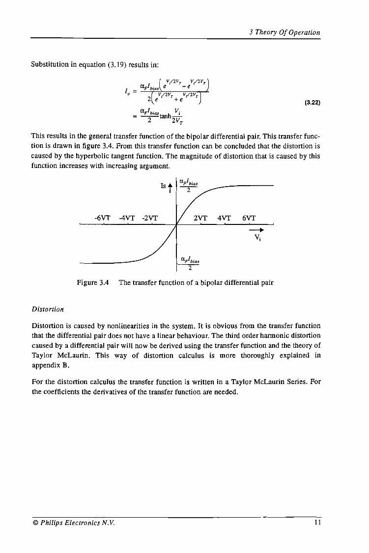
This results in the general transfer function of the bipolar differential pair. This transfer function is drawn in figure 3.4. From this transfer function can be concluded that the distortion iscaused by the hyperbolic tangent function. The magnitude of distortion that is caused by thisfunction increases with increasing argument.
-6VT -4VT -2VT 2VT 4VT 6VT
Figure 3.4 The transfer function of a bipolar differential pair
Distortion
Distortion is caused by nonlinearities in the system. It is obvious from the transfer functionthat the differential pair does not have a linear behaviour. The third order harmonic distortioncaused by a differential pair will now be derived using the transfer function and the theory ofTaylor McLaurin. This way of distortion calculus is more thoroughly explained inappendix B.
For the distortion calculus the transfer function is written in a Taylor McLaurin Series. Forthe coefficients the derivatives of the transfer function are needed.
© Philips Electronics N.V. 11
3 Theory Of Operation
(3.23)
4v;.( v.) ( V. )4
3 CJ.FIbias - 2 + cosh V' sech 2V'dlo _ T T
dVi - 8V~
With these derivatives the Taylor-McLaurin coefficients can be calculated.
Leading to:
ao = 0
CJ.FIbiasa l = 4V
T
aZ = 0
With these coefficients the hannonic distortion can be calculated.
In these equations A represents the input signal amplitude.
(3.24)
(3.25)
(3.26)
From these equations can be concluded that the second order hannonic distortion is zero.About the third order hannonic distortion can be concluded that it is mainly dependent on theamplitude of input signal.
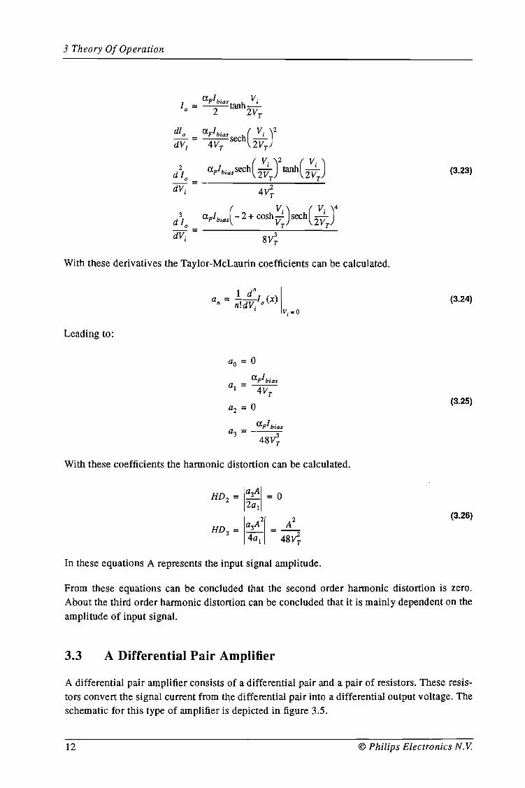
3.3 A Differential Pair Amplifier
A differential pair amplifier consists of a differential pair and a pair of resistors. These resistors convert the signal current from the differential pair into a differential output voltage. Theschematic for this type of amplifier is depicted in figure 3.5.
12 © Philips Electronics N.V.
3 Theory Of Operation
Figure 3.5 Differential pair amplifier
The transfer function of this amplifier can easily be derived with the transfer function of thedifferential pair. The signal current flows through the resistors where the output voltage isgenerated. The transfer function is fonnulated in equation (3.27).
(3.27)
Gain
The gain of this system can be found by the second Taylor-McLaurin coefficient. This coefficient gives the linear transfer function from input to output signal. This coefficient equals:
dVulG=-dV.
I v.=oI
= (3.28)
The common mode level of the output voltage equals the supply voltage minus the voltagegenerated over the load resistors by the bias current. The bias current through the resistorsequals the bias current through the collector of the transistor if we do not load the circuit.This bias current can be expressed as upl bia/2. The common mode level of the output signalcan then be expressed with:
(3.29)
This output common mode level limits the value of IbiasR/. Since this factor is also the maindesign property of the gain of the amplifier, the gain of this type is limited with respect to thevoltage space. This maximum gain can be expressed as:
© Philips Electronics N. V. 13
3 Theory Of Operation
Distortion
Gmax = Vsup - VCMout
VT(3.30)
With the transfer function the third order hannonic distortion can be calculated as describedin appendix B. This results in:
(3.31)
This is the same as for the differential pair because the load resistors are linear and thus donot contribute to any distortion.
From equation (3.31) can be seen that the third order hannonic distortion is mainly dependenton the input signal amplitude. For a specified maximum of third order hannonic distortion amaximum amplitude for the input signal can be calculated. Combining this with the limit onthe gain we can conclude that for this type of amplifier a maximum level of third order harmonic distortion leads to a maximum in the amplitude of the output signal.
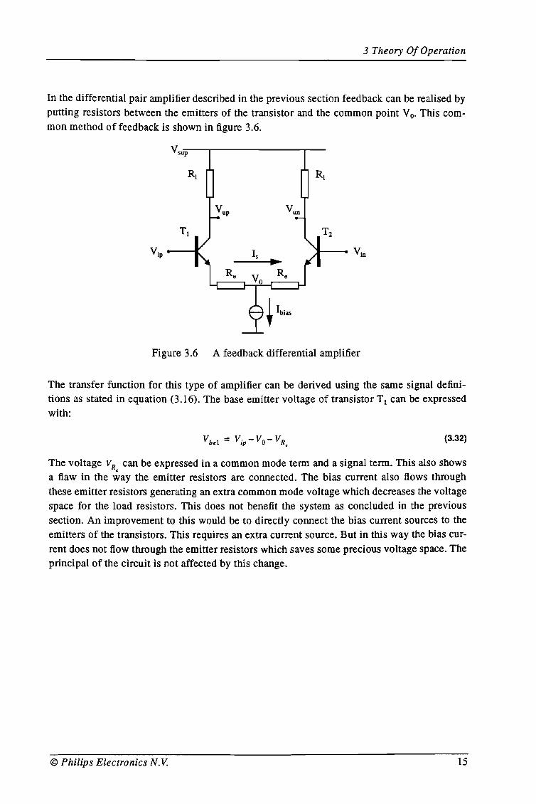
3.4 A Differential Pair Amplifier With Feedback
A commonly used method to reduce distortion is the use of feedback. With feedback the output signal is fed back and subtracted from the input signal. In the feedback loop the outputsignal can be processed to reach an optimum for the system.
14 © Philips Electronics N. V.
3 Theory Of Operation
In the differential pair amplifier described in the previous section feedback can be realised byputting resistors between the emitters of the transistor and the common point Yo. This common method of feedback is shown in figure 3.6.
Vsu::::p----.----------.--
Figure 3.6 A feedback differential amplifier
The transfer function for this type of amplifier can be derived using the same signal definitions as stated in equation (3.16). The base emitter voltage of transistor T1 can be expressedwith:
(3.32)
The voltage vR can be expressed in a common mode term and a signal term. This also showsa flaw in the ~ay the emitter resistors are connected. The bias current also flows throughthese emitter resistors generating an extra common mode voltage which decreases the voltagespace for the load resistors. This does not benefit the system as concluded in the previoussection. An improvement to this would be to directly connect the bias current sources to theemitters of the transistors. This requires an extra current source. But in this way the bias current does not flow through the emitter resistors which saves some precious voltage space. Theprincipal of the circuit is not affected by this change.
© Philips Electronics N. V. 15
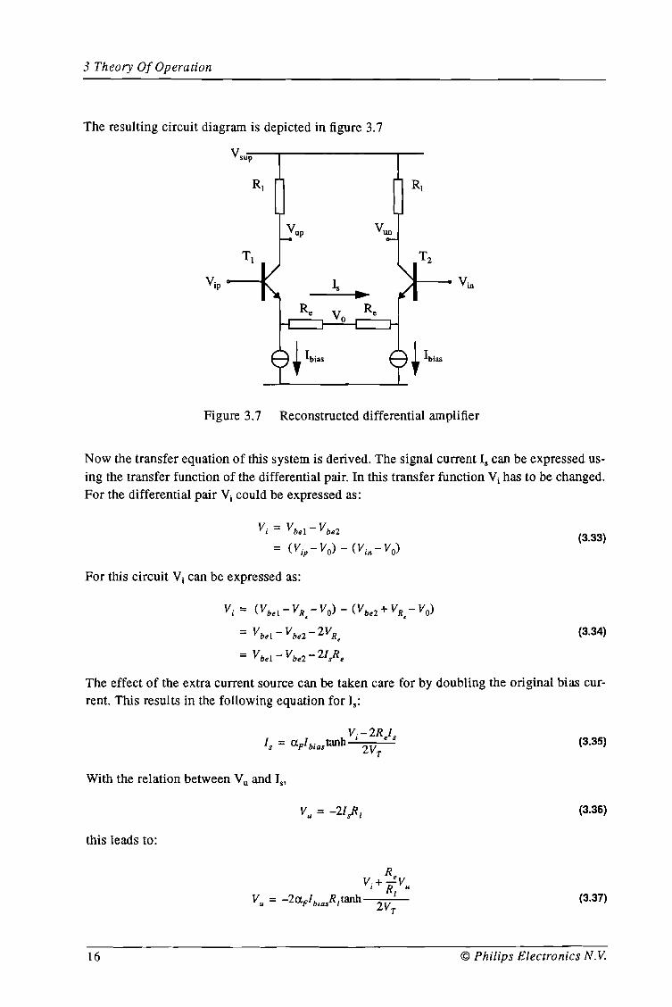
3 Theory OJ Operation
The resulting circuit diagram is depicted in figure 3.7
Vsu""p----.----------.---
Figure 3.7 Reconstructed differential amplifier
Now the transfer equation of this system is derived. The signal current Is can be expressed us
ing the transfer function of the differential pair. In this transfer function Vi has to be changed.For the differential pair Vi could be expressed as:
Vi = Vbe1 - V be2
= (Vip - YO) - (Vin - yO)
For this circuit Vi can be expressed as:
Vi = (Vbe1 - VR - yO) - (Vbe2 + VR - yO), ,
= V be1 - Vbe2 - 2VR,
= V be1 - Vbe2 - 21~e
(3.33)
(3.34)
The effect of the extra current source can be taken care for by doubling the original bias current. This results in the following equation for Is:
(3.35)
With the relation between Vu and Is,
(3.36)
this leads to:
16
(3.37)
© Philips Electronics N. V.
3 Theory Of Operation
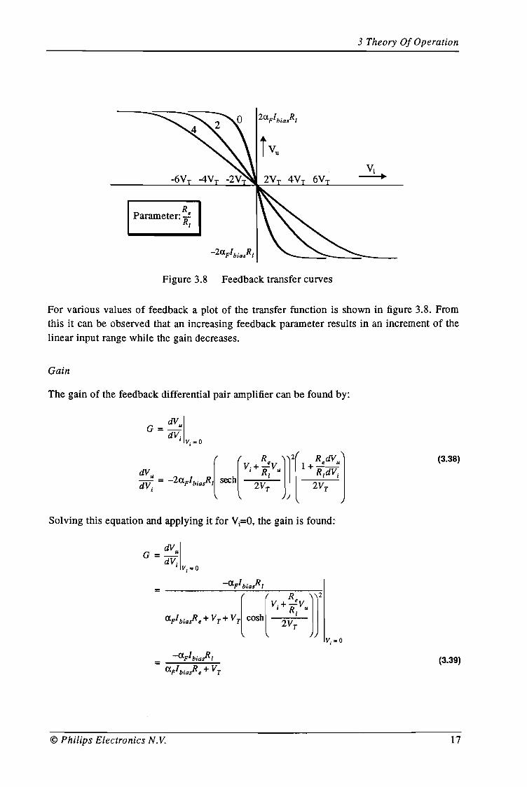
RParameter: /
I
Figure 3.8 Feedback transfer curves
For various values of feedback a plot of the transfer function is shown in figure 3.8. Fromthis it can be observed that an increasing feedback parameter results in an increment of thelinear input range while the gain decreases.
Gain
The gain of the feedback differential pair amplifier can be found by:
dVulG=-dV.
I Vi=O
Solving this equation and applying it for Vi=O, the gain is found:
dVulG=-dV.
I v.=oI
© Philips Electronics N.V.
(3.38)
(3.39)
17
3 Theory Of Operation
Again it can be observed from equation (3.39) that the gain of this type of amplifier is limited. This is caused by the common mode levels that should be kept above a minimum. Be
cause of this maximum for the numerator in the expression, the gain is limited. Thedenominator has its minimum in the case where Re is zero, resulting in the amplifier with nofeedback discussed in section 3.3.
If the thermal voltage can be neglected with respect to fXFlbia.Re' the gain equals:
(3.40)
Distortion
By calculating the derivatives of the transfer function the third order harmonic distortion canbe found.
(3.41)
Together with equations (B.7) and (B.2) from appendix B the third order harmonic distortioncan be calculated as:
(3.42)
From this equation it can be seen that the third order harmonic distortion is reduced with thethird power of the feedback resistor Re• This is in case VT can be neglected with respect tofXFlbiasRe' For a fixed gain with optimal use of the available voltage space the minimal level ofthird order harmonic distortion can be calculated. If equation (3.42) is rewritten in terms ofgain G, supply voltage Vsup and the common mode output voltage VCMout' it follows:
VCMout = V.up - aFIbia~I
VTA21GI 3
HD 3 = 3
48 (V.up - VCMout)
(3.43)
Considering that the output signal amplitude equals the input signal amplitude times the gain,it can be concluded that the third order harmonic distortion increases with the output signalamplitude to the second power. Thus limiting the gain of the amplifier benefits the quality ofthe system with respect to the third order harmonic distortion level. The level of third orderharmonic distortion is also dependent on the common mode level of the output signal. Bychoosing this common mode level as low as possible the amount of third order harmonic distortion can be kept to a minimum.
18 © Philips Electronics N. V.
3 Theory OJ Operation
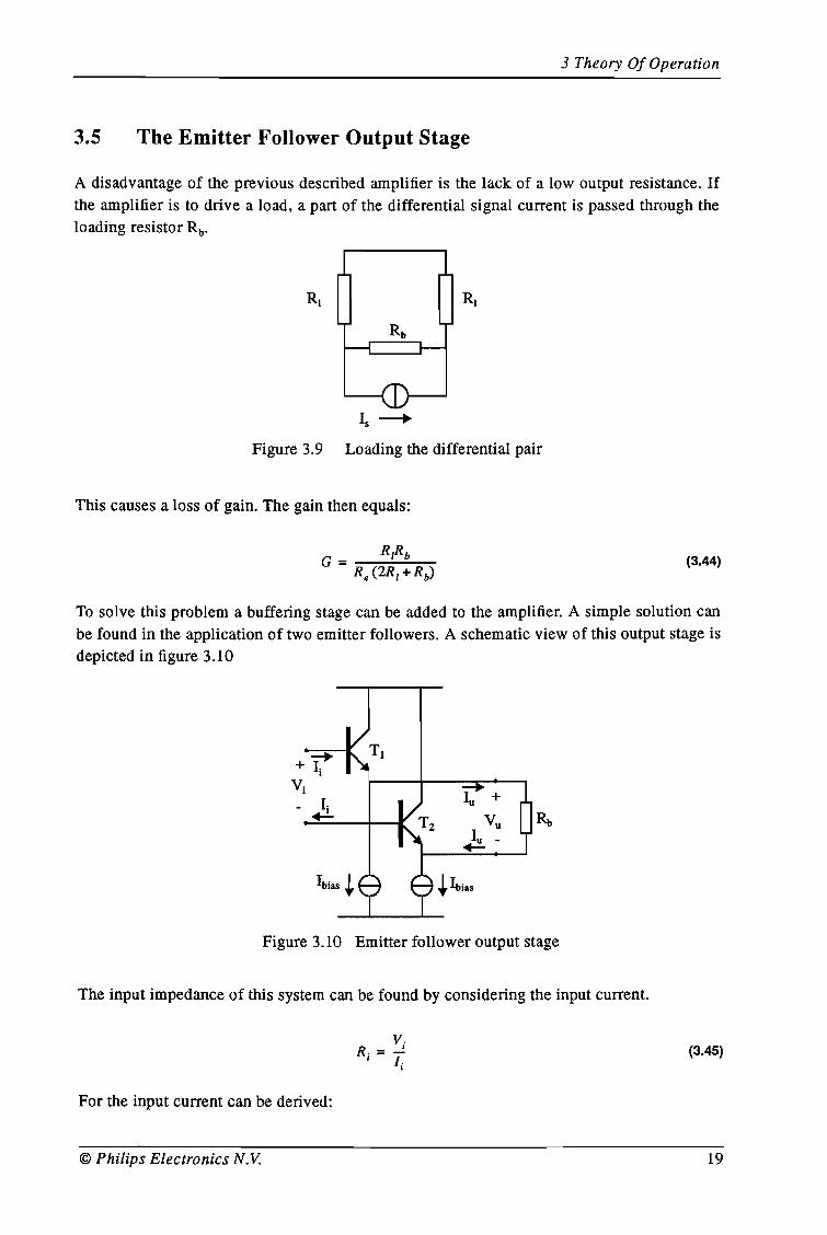
3.5 The Emitter Follower Output Stage
A disadvantage of the previous described amplifier is the lack of a low output resistance. Ifthe amplifier is to drive a load, a part of the differential signal current is passed through theloading resistor Rb•
Is --.
Figure 3.9 Loading the differential pair
This causes a loss of gain. The gain then equals:
(3.44)
To solve this problem a buffering stage can be added to the amplifier. A simple solution canbe found in the application of two emitter followers. A schematic view of this output stage isdepicted in figure 3.10
Figure 3.10 Emitter follower output stage
The input impedance of this system can be found by considering the input current.
V.R. =....!
I Ij
For the input current can be derived:
© Philips Electronics N. V.
(3.45)
19
3 Theory Of Operation
I. = I b TI , 1
(3.46)
With the unity gain this leads to an input impedance of ~FRb' Which is a factor ~F better.
The transfer function of this output stage can be derived using the basic transistor equations.
(3.47)
By calculation of the derivative of this equation with respect to Vi, and applying it for Vi iszero we find the gain of the circuit: •
dVulG=-dV.
I Vi=O
Which approximates unity when IbiasRb dominates over 2 VT.
With the theory of appendix B, for the third order harmonic distortion can be found:
(3.48)
(3.49)
By maximizing the bias current the harmonic distortion minimizes and the gain approximatesunity. With a given output signal amplitude the desired level of hannonic distortion can bereached by putting a demand on the input impedance of the following stage.
A disadvantage of this output stage is the loss of another base-emitter junction voltage. Thisloss limits the voltage space available to the previous stage. This results in loss of performance of the total system.
3.6 The Differential Pair Amplifier With Output Stage
To use a differential pair amplifier as described in section 3.4, it needs a buffering outputstage as described in section 3.5. A system with cascaded amplifier stages which each a nonlinear behaviour can be described as one system with a total gain GT> and an overall third or-
20 © Philips Electronics N. V.
3 Theory Of Operation
der hannonic distortion level HD3T• The perfonnance of the total system can be derived usingthe theory of appendix C.
For the total gain can be found:
Gr = GDPAGEP
-(J.p1bias.DPAR / Ibias,EFRb=(J.F1bias,DPARe + Vr I bias.EFRb + 2Vr
(3.50)
Where GDPA is the gain of the differential pair amplifier and GEF the gain of the emitter follower.
For the total distortion can be found:
(3.51)
3.7 The Transresistance Amplifier
A resistor is a passive device to convert a current into a voltage. This principle is applied inthe amplifier of section 3.3. In this system the bias current and the signal current were ledthrough the same resistor. This causes a loss of voltage space that could be saved if the signalcurrent could somehow be separated from the bias current.
A way of separating the signal current is to divert it through the feedback resistors of an amplifier. A schematic of this principle is shown in figure 3.11
Figure 3.11 Transresistance amplifier
The voltage at the input of the amplifier will be very small because of the feedback and theassumed high gain of the amplifier. Connecting this stage to an differential pair amplifier willalmost completely divert the signal current through the feedback resistors. The output voltage Vu will then become:
© Philips Electronics N.V. 21
3 Theory Of Operation
(3.52)
For the amplifier a differential pair amplifier can be used. This will be discussed in the nextsection.
3.7.1 Implementing A Differential Pair Amplifier.
A circuit diagram of the implementation of the transresistance amplifier utilizing a differential pair amplifier is shown in figure 3.12.
R, R1
T3Yap
Van T4
Vup +Vu
Yip R Vun
Is t RiR
YinIbiasl+. Ibias2+.
Figure 3.12 Implementation of a transresistance amplifier
The input current source is shown together as an ideal current source with its internal impedance. The current flowing through this resistor generates the input voltage of the differentialpair. The main part of the input current will flow through the feedback resistors and thus generates the output voltage. The amplifier is built with a differential pair amplifier. This is not alinear amplifier and causes some distortion. Analysis of the level of third order harmonic distortion is done in the following sections.
The circuit equation
For the amplifier the circuit equation was derived in section 3.3. The buffering stage is loaded with the feedback resistors and the internal impedance of the signal current source. Butthis value is assumed to be large and the transfer equation of the output stage is assumed tobe unity. Some considerations on the effect of loading the total circuit are made later.
22 © Philips Electronics N. V.
3 Theory Of Operation
The circuit equations of the amplifier then can be written as:
(3.53)
Summing the currents at the nodes Vip and Vin leads to:
(3.54)
Adding these equations leads to:
(3.55)
Combining this with equation (3.53) a general relation between the input current and the output voltage is obtained.
(3.56)
With this relation the transresistance and the third order harmonic distortion can be calculated using the theory of appendix B.
The transresistance equals the derivative of Vuwith respect to Is.
(3.57)
When in the denominator the term 2vr can be neglected, the transresistance equals 2Rr
For the third order harmonic distortion can be derived:
© Philips Electronics N. V.
(3.58)
23
3 Theory Of Operation
When again neglecting the 2VT term in the denominator the equation simplifies to:
(3.59)
From this can be concluded that the level of third order harmonic distortion is related to thesquare of the output signal amplitude 2Rlo' The gain of the amplifying stage reduces the level of third order harmonic distortion with the third power. But this gain is limited because ofcommon mode level considerations.
The output impedance of this circuit is built out of the parallel connection of the output impedance of the buffered differential pair amplifier and the serial connection of the two feedback resistors with the current source's internal resistance. Resulting in:
(3.60)
This value can be made low by choosing a low value of RI. The value of this resistor can bemade low when increasing the bias current of the amplifying stage. Because these factorsonly occur together in any gain or distortion equations.
24 © Philips Electronics N. V.
3 Theory Of Operation
3.8 A Three Stage Differential Amplifier
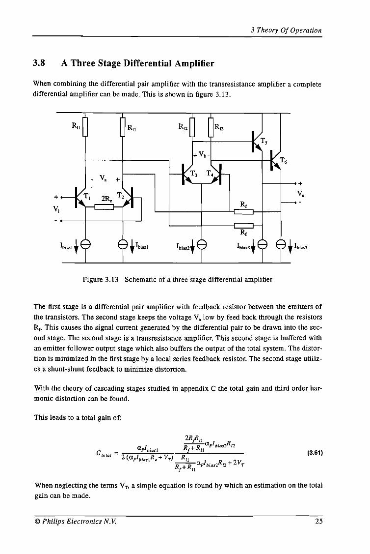
When combining the differential pair amplifier with the transresistance amplifier a complete
differential amplifier can be made. This is shown in figure 3.13.
RIl RIl R12 R IZ
Ts
+ V b -T6
- Va + +
+ V u
ViR f
R f
I
biasz
' I
bias3
'
• Ibias3
Figure 3.13 Schematic of a three stage differential amplifier
The first stage is a differential pair amplifier with feedback resistor between the emitters of
the transistors. The second stage keeps the voltage Va low by feed back through the resistors
R f • This causes the signal current generated by the differential pair to be drawn into the sec
ond stage. The second stage is a transresistance amplifier. This second stage is buffered with
an emitter follower output stage which also buffers the output of the total system. The distor
tion is minimized in the first stage by a local series feedback resistor. The second stage utiliz
es a shunt-shunt feedback to minimize distortion.
With the theory of cascading stages studied in appendix C the total gain and third order har
monic distortion can be found.
This leads to a total gain of:
(3.61)
When neglecting the tenns VT' a simple equation is found by which an estimation on the totalgain can be made.
© Philips Electronics N.V. 25
3 Theory Of Operation
(3.62)
For the total third harmonic distortion can be derived:
(3.63)
Simplifying this equation by neglecting VT this leads to:
(3.64)
The first term in this equation can be minimized resulting in a smaller value for the signalcurrent passing into the second stage of the amplifier. The second term however mainly depends on the output signal amplitude and the voltage space available for the second stage differential pair amplifier. This will limit the performance of the circuit.
26 © Philips Electronics N. V.
4 Implementation And Simulation
4 Implementation And Simulation
In this chapter the previously discussed circuits are discussed with respect to the specifications derived in the Introduction. The circuits are optimized using simulation results and thepros and cons are discussed.
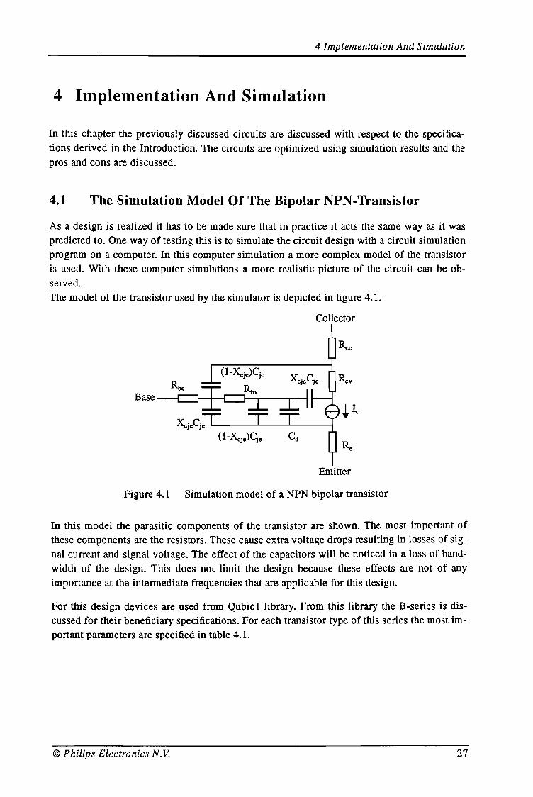
4.1 The Simulation Model Of The Bipolar NPN-Transistor
As a design is realized it has to be made sure that in practice it acts the same way as it waspredicted to. One way of testing this is to simulate the circuit design with a circuit simulationprogram on a computer. In this computer simulation a more complex model of the transistoris used. With these computer simulations a more realistic picture of the circuit can be observed.The model of the transistor used by the simulator is depicted in figure 4.1.
Collector
Base --[=J---+--C=l-,--.....,.--1
Emitter
Figure 4.1 Simulation model of a NPN bipolar transistor
In this model the parasitic components of the transistor are shown. The most important ofthese components are the resistors. These cause extra voltage drops resulting in losses of signal current and signal voltage. The effect of the capacitors will be noticed in a loss of bandwidth of the design. This does not limit the design because these effects are not of anyimportance at the intermediate frequencies that are applicable for this design.
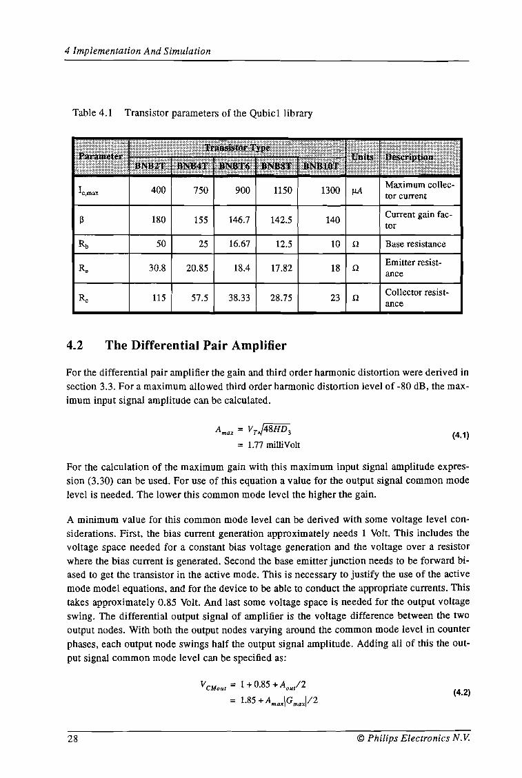
For this design devices are used from Qubic1 library. From this library the B-series is discussed for their beneficiary specifications. For each transistor type of this series the most important parameters are specified in table 4.1.
© Philips Electronics N.V. 27
4 Implementation And Simulation
Table 4.1 Transistor parameters of the Qubicl library
-----Ic,max 400 750 900 1150 1300 J.lA
Maximum collec-tor current
~ 180 155 146.7 142.5 140Current gain fac-tor
Rb 50 25 16.67 12.5 10 n Base resistance
Re 30.8 20.85 18.4 17.82 18 n Emitter resist-ance
Rc 115 57.5 38.33 28.75 23 n Collector resist-ance
4.2 The Differential Pair Amplifier
For the differential pair amplifier the gain and third order harmonic distortion were derived insection 3.3. For a maximum allowed third order harmonic distortion level of -80 dB, the maximum input signal amplitude can be calculated.
Amax = Vr J48HD 3
= 1.77 milliVolt(4.1)
For the calculation of the maximum gain with this maximum input signal amplitude expression (3.30) can be used. For use of this equation a value for the output signal common modelevel is needed. The lower this common mode level the higher the gain.
A minimum value for this common mode level can be derived with some voltage level considerations. First, the bias current generation approximately needs 1 Volt. This includes thevoltage space needed for a constant bias voltage generation and the voltage over a resistorwhere the bias current is generated. Second the base emitter junction needs to be forward biased to get the transistor in the active mode. This is necessary to justify the use of the activemode model equations, and for the device to be able to conduct the appropriate currents. Thistakes approximately 0.85 Volt. And last some voltage space is needed for the output voltageswing. The differential output signal of amplifier is the voltage difference between the twooutput nodes. With both the output nodes varying around the common mode level in counterphases, each output node swings half the output signal amplitude. Adding all of this the output signal common mode level can be specified as:
28
VCMout = 1 + 0.85 + Aou/2
= 1.85 + AmaxiGmaxll2(4.2)
© Philips Electronics N. V.
4 Implementation And Simulation
Putting this in equation (3.30) the maximum gain can be calculated.
_ -2 (Vsup - 1.85)Gmax - A 2V
max+ T
= -119.4
(4.3)
With this maximum gain and the maximum for the input signal amplitude the maximum output signal amplitude can be calculated.
(4.4)= 211 milliVolt
As can be seen from this result, the differential pair amplifier does not meet the specificationof 1 Volt output amplitude level. To get an idea of the performance of this type of amplifier,the third order harmonic distortion can be calculated with all of the other specifications maintained.
Aout = AlGI= 1
(4.5)
This leads to a common mode level for the output signal of 2.35 Volt. Resulting in a maximum gain of 104. Implying an input signal amplitude of 9.62 milliVolt. With equation (3.31)the distortion level can then be calculated as:
HD 3 = -50.6 dB (4.6)
From this can be concluded that an increase of the output signal amplitude increases the distortion level dramatically.
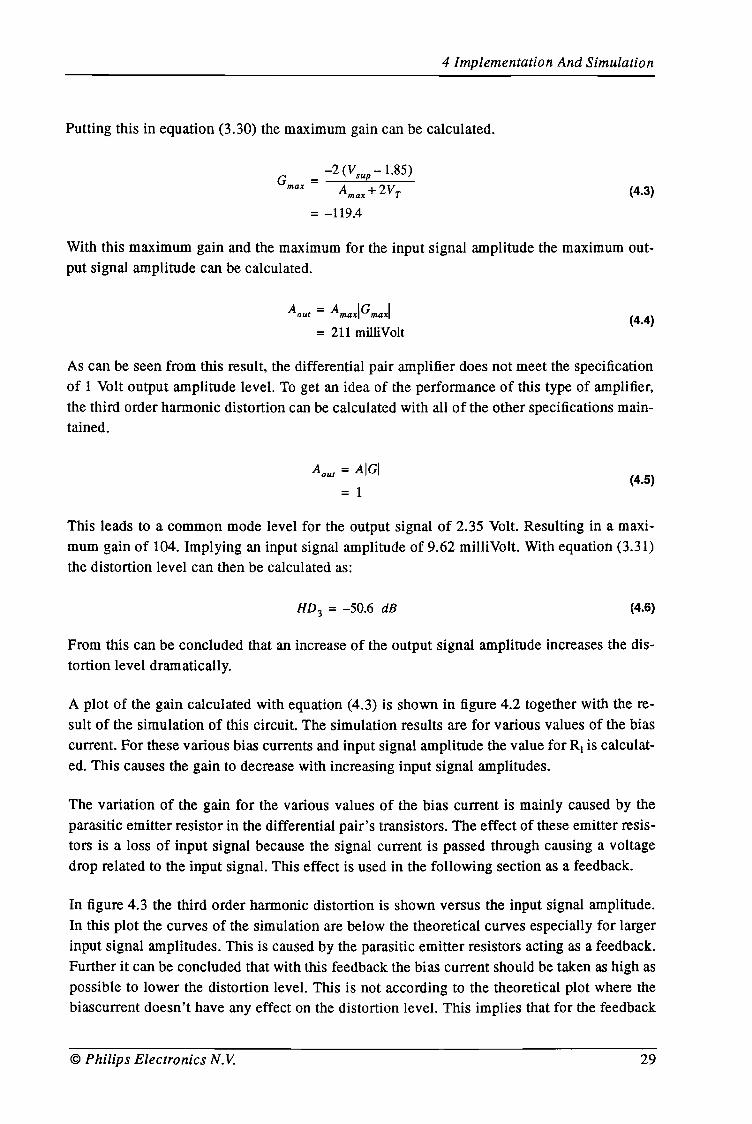
A plot of the gain calculated with equation (4.3) is shown in figure 4.2 together with the result of the simulation of this circuit. The simulation results are for various values of the biascurrent. For these various bias currents and input signal amplitude the value for R1 is calculated. This causes the gain to decrease with increasing input signal amplitudes.
The variation of the gain for the various values of the bias current is mainly caused by theparasitic emitter resistor in the differential pair's transistors. The effect of these emitter resistors is a loss of input signal because the signal current is passed through causing a voltagedrop related to the input signal. This effect is used in the following section as a feedback.
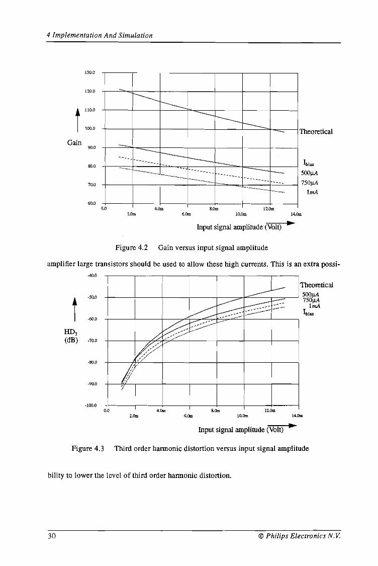
In figure 4.3 the third order harmonic distortion is shown versus the input signal amplitude.In this plot the curves of the simulation are below the theoretical curves especially for largerinput signal amplitudes. This is caused by the parasitic emitter resistors acting as a feedback.Further it can be concluded that with this feedback the bias current should be taken as high aspossible to lower the distortion level. This is not according to the theoretical plot where thebiascurrent doesn't have any effect on the distortion level. This implies that for the feedback
© Philips Electronics N. V. 29
4 Implementation And Simulation
- Theoretical
------r--
12.Om8.Om4.Om
----I----------- ------
130.0
120.0
t110.0
100.0
Gain90.0
80.0
70.0
60.00.0
2.Om 6.Om 1O.Om 14.Om
Input signal amplitude (Volt) ~
Figure 4.2 Gain versus input signal amplitude
amplifier large transistors should be used to allow these high currents. This is an extra possi-
12.Om8.Om4.Om
'II
Theoretical
------~
+-----t-----t---+---+-----:::,.....,..=----t-~___.,500!J.A~ ~- 750
1llA
A'-----1 ~---- _.,.. m~__~-.~_~.:..~~.:.-:-... _- Ibias
0~':-~-:':~" .~ /;'./'
40.0
t-50.0
-60.0
HD3(dB) -70.0
-80.0
-90.0
-100.00.0
2.Om 6.Om 10.Om 14.Om
Input signal amplitude (Volt) ~
Figure 4.3 Third order harmonic distortion versus input signal amplitude
bility to lower the level of third order harmonic distortion.
30 © Philips Electronics N. V.
4 Implementation And Simulation
4.3 The Feedback Differential Pair Amplifier
The previous section showed the benefit of applying a series feedback to the differential pairamplifier. In the previous section the feedback was not intended and not controllable. Here
the effect of the value of a feedback resistor applied is discussed.
When adding extra feedback resistors to the differential pair amplifier the gain can be expressed with equation (3.39). Assuming that the thermal voltage in the denominator can be
neglected the gain can be calculated as the quotient of the load resistor and the emitter resistor. In this case the level of third order harmonic distortion can be calculated with:
(4.7)
For a given maximum value for the harmonic distortion and a given input signal amplitude,
an equation for (J.plbia/?e can be obtained.
(4.8)
A minimum value for the output common mode level is defined in equation (4.2). Whileequation (3.43) specifies this common mode level. Combining these equation leads to:
(4.9)
For the maximum gain now can be derived:
(4.10)
Solving this equation for Gmax with equations (4.8) and (4.9) leads to:
Gmax =(4.11)
For a level of third order harmonic distortion of -80 dB and an input signal amplitude of 100
milliVolt a maximum gain of 7.40 is found. Resulting in an output signal amplitude of 740milliVolt.
The level of third order harmonic distortion for a given input signal amplitude and output signal amplitude can be calculated using equation (3.43). A value of -71 dB is then found for thelevel of third order harmonic distortion.
© Philips Electronics N.V. 31
4 Implementation And Simulation
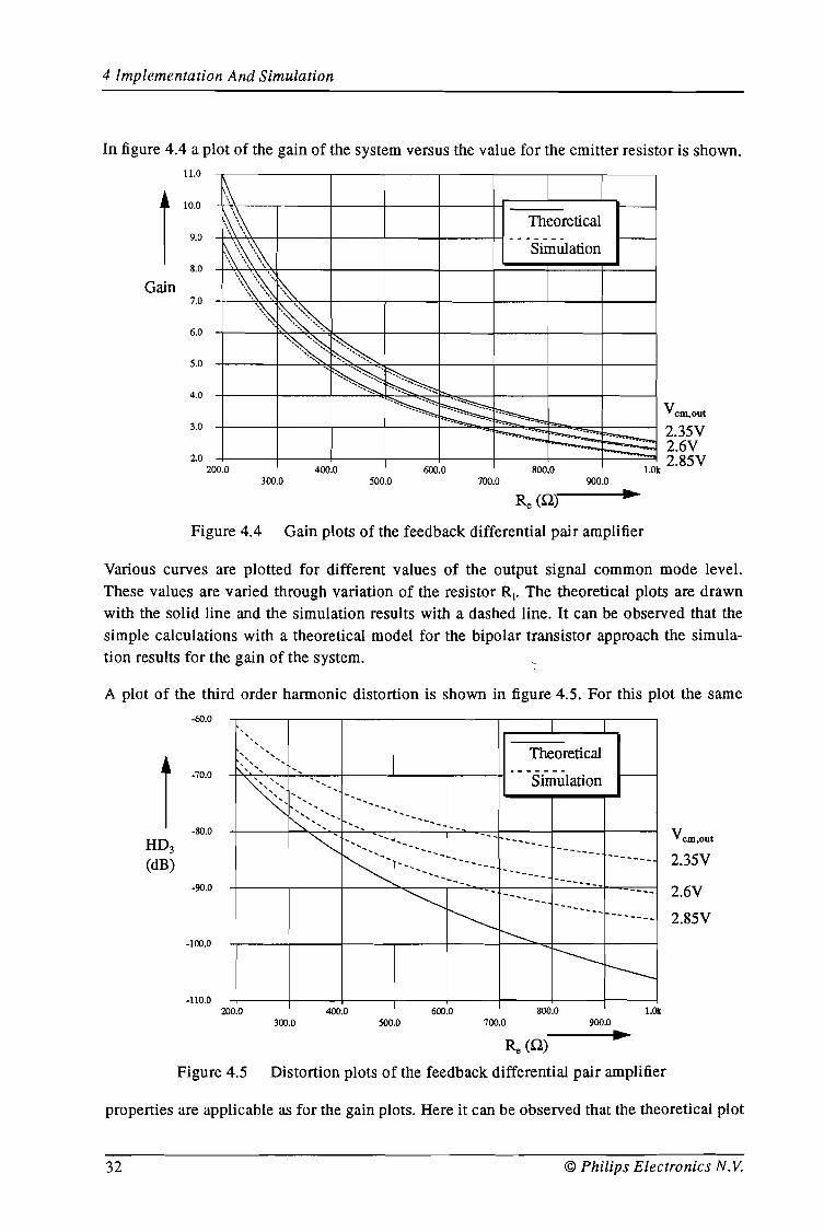
In figure 4.4 a plot of the gain of the system versus the value for the emitter resistor is shown.
Vern,out
I--
900.0
Theoretical
-._~~~:::: ~:~~V
800.0 1.0k 2.85V700.0
600.0500.0
400.0300.0
"\f\'~··k··~··~
--pr\~_+---+--+-I--r==~---"--)I-I~\\1\\\\+~;--+---t---+----1---+-J. - - - - - -I\~\ Simulation
4.0
2.0200.0
7.0
5.0
6.0
3.0
11.0
Gain
Figure 4.4 Gain plots of the feedback differential pair amplifier
Various curves are plotted for different values of the output signal common mode level.These values are varied through variation of the resistor RI. The theoretical plots are drawnwith the solid line and the simulation results with a dashed line. It can be observed that thesimple calculations with a theoretical model for the bipolar transistor approach the simulation results for the gain of the system.
A plot of the third order harmonic distortion is shown in figure 4.5. For this plot the same
~~ ------- -------- --~--
...............
2.35V
2.6V
2.85V
Vern,out
-
----
Theoretical
,,
, ,,,', ......
-+"<,~:>;=:-,-=,"'":",-"+,,,,,,",,:-,-,,-+---+----+----H" 'Siillulation.... , ... ... ...
".;:',:'"" "'--.......... ........... ............ ... ... _-
-90.0
-80.0
-70.0
-60.0
-100.0
HD3
(dB)
-110.0200.0 400.0 600.0 800.0 l.Ok
900.0
•700.0500.0300.0
Re (0)
Figure 4.5 Distortion plots of the feedback differential pair amplifier
properties are applicable as for the gain plots. Here it can be observed that the theoretical plot
32 © Philips Electronics N. V.
4 Implementation And Simulation
is riot affected by variation of the output common mode level. The simulation results howevershow, with increasing common mode level of the output signal, a lower value of third orderharmonic distortion, nearer to the theoretical curve. Further it can be observed that with anincreasing value of the emitter resistance, the simulated level of distortion tends to a curvewith a stabilizing level of harmonic distortion where the theoretical slope is -3 (seefigure 4.6). This stabilization occurs when the gain approaches unity. The voltage over the
70.0..6:5.0
20 Log <Re)60.0
:5:5.050.0
I'--... . " ~ ~+---__+--__--+ -+ -11
__~"""~~~ Slope-3
-60.0
I-70.0
-80.0
-90.0
HD3
(dB) -100.0
-110.0
-120.0
-130.0
-140.04:5.0
Figure 4.6 Logarithmic distortion plots of the feedback differential pair amplifier
emitter resistors dominates the base-emitter junction voltages, causing the transistors to losetheir functionality. The circuit loses its amplifying characteristic and is not functional anymore.
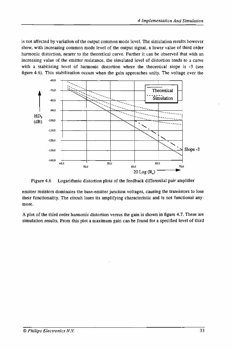
A plot of the third order harmonic distortion versus the gain is shown in figure 4.7. These aresimulation results. From this plot a maximum gain can be found for a specified level of third
© Philips Electronics N. V. 33
4 Implementation And Simulation
order harmonic distortion. For the -80 dB level a gain of approximately 5 is maximal. While
, ,
2.6Y- <,/, ,
.'...... "..- ...::::......
-60.0
1-65.0
-70.0
-75.0
HD3 -80.0(dB)
-85.0
-90.0
-95.0
-100.02.0
,
,,/2.85V
3.04.0
5.06.0
7.08.0
Gain9.0
10.011.0
Figure 4.7 Simulated distortion versus gain plot
a gain of 10 implies a level of third order harmonic distortion of minimal -64 dB.
4.4 The Emitter Follower Output Stage
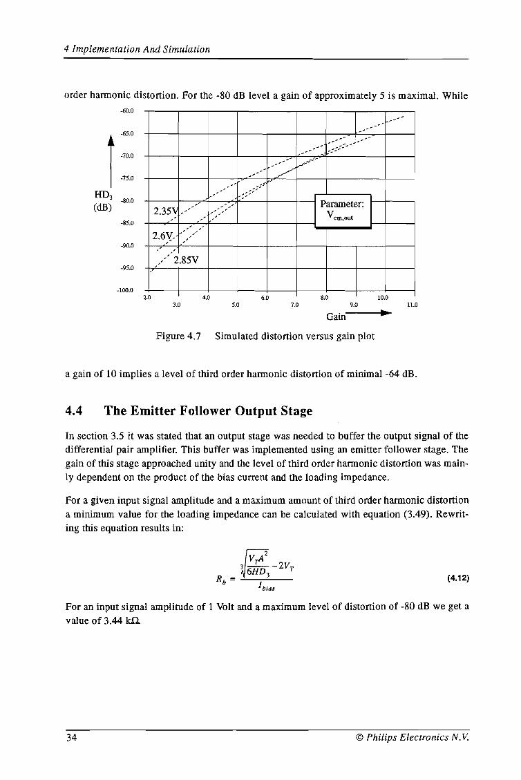
In section 3.5 it was stated that an output stage was needed to buffer the output signal of thedifferential pair amplifier. This buffer was implemented using an emitter follower stage. Thegain of this stage approached unity and the level of third order harmonic distortion was mainly dependent on the product of the bias current and the loading impedance.
For a given input signal amplitude and a maximum amount of third order harmonic distortiona minimum value for the loading impedance can be calculated with equation (3.49). Rewriting this equation results in:
(4.12)
For an input signal amplitude of 1 Volt and a maximum level of distortion of -80 dB we get avalue of 3.44 kU
34 © Philips Electronics N. V.
4 Implementation And Simulation
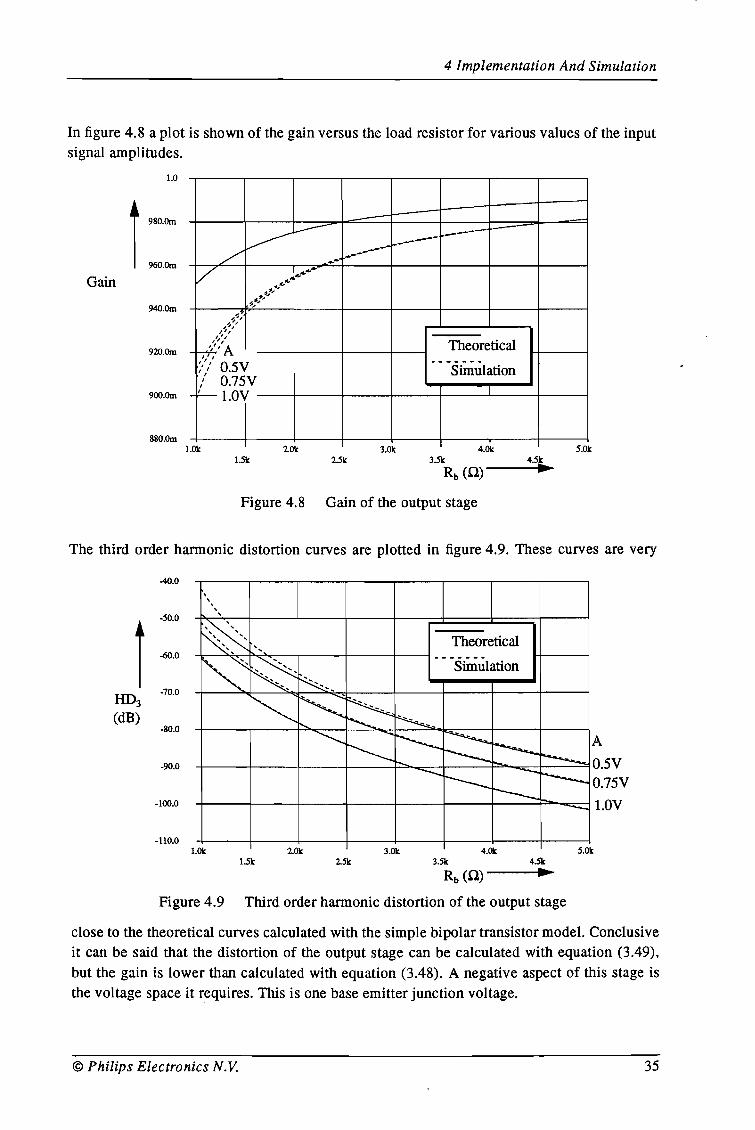
In figure 4.8 a plot is shown of the gain versus the load resistor for various values of the inputsignal amplitudes.
Gain
1.0
t 980.Om
I 960.Om
940.Om
920.Om
9oo.0m
880.Om
--- -- --~ -----
/ ---------/
............~~...tI!'
.;:11I......
**... ."f,... "
",',,",',, "" ," , Theoretical~~I A-:1;-
;:" O.5V----_.-
/ O.75VSimulation
:'-l.OV
1.0kl.5k
2.0k25k
3.0k 4.0k4.ft.. 5.0k
Figure 4.8 Gain of the output stage
The third order harmonic distortion curves are plotted in figure 4.9. These curves are very
-40.0
I-50.0
-60.0
HD3
-70.0
(dB)·80.0
-90.0
-100.0
-110.0
,,,,,
~ Theoretical,
~~--.----
Simulation~"
~~,~....... r--.. "-
............... ........r----~I--- r---r---.. ---......r--. I--..
---r--- -----r---.. -
A
O.5VO.75V
1.0V
1.0k15k
2.0k2.5k
3.0k 4.Ok3.5k 4.5k
Rb (0)---I"~
5.0k·
Figure 4.9 Third order harmonic distortion of the output stage
close to the theoretical curves calculated with the simple bipolar transistor model. Conclusiveit can be said that the distortion of the output stage can be calculated with equation (3.49),but the gain is lower than calculated with equation (3.48). A negative aspect of this stage isthe voltage space it requires. This is one base emitter junction voltage.
© Philips Electronics N. V. 35
4 Implementation And Simulation
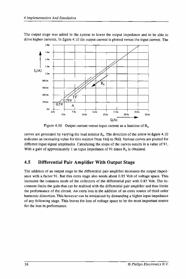
The output stage was added to the system to lower the output impedance and to be able to
drive higher currents. In figure 4.10 the output current is plotted versus the input current. The
7.5u 12.5u 17.5u 225u
//
~v
4 V
///'/"~/~~~VRb
~VV/ IV
/O.75V0.5V A
I25u
l.Sm
tl.6m
l.4m
l.2m
Io(A)l.Orn
SOO.OU
6OO.Ou
4oo.0u
2oo.0u
0.0
5.Ou 10.Ou 15.Ou 20.Ou 25.Ou
IlA)Figure 4.10 Output current versus input current as a function ofRb
curves are generated by varying the load resistor Rb• The direction of the arrow in figure 4.10indicates an increasing value for this resistor from lkQ to 5kU Various curves are plotted for
different input signal amplitudes. Calculating the slope of the curves results in a value of 91.With a gain of approximately 1 an input impedance of 91 times Rb is obtained.
4.5 Differential Pair Amplifier With Output Stage
The addition of an output stage to the differential pair amplifier decreases the output impedance with a factor 91. But this extra stage also needs about 0.85 Volt of voltage space. Thisincreases the common mode of the collectors of the differential pair with 0.85 Volt. The in
crement limits the gain that can be realized with the differential pair amplifier and thus limits
the performance of the circuit. An extra loss is the addition of an extra source of third orderharmonic distortion. This however can be minimized by demanding a higher input impedanceof any following stage. This leaves the loss of voltage space to be the most important source
for the loss in performance.
36 © Philips Electronics N. V.
4 Implementation And Simulation
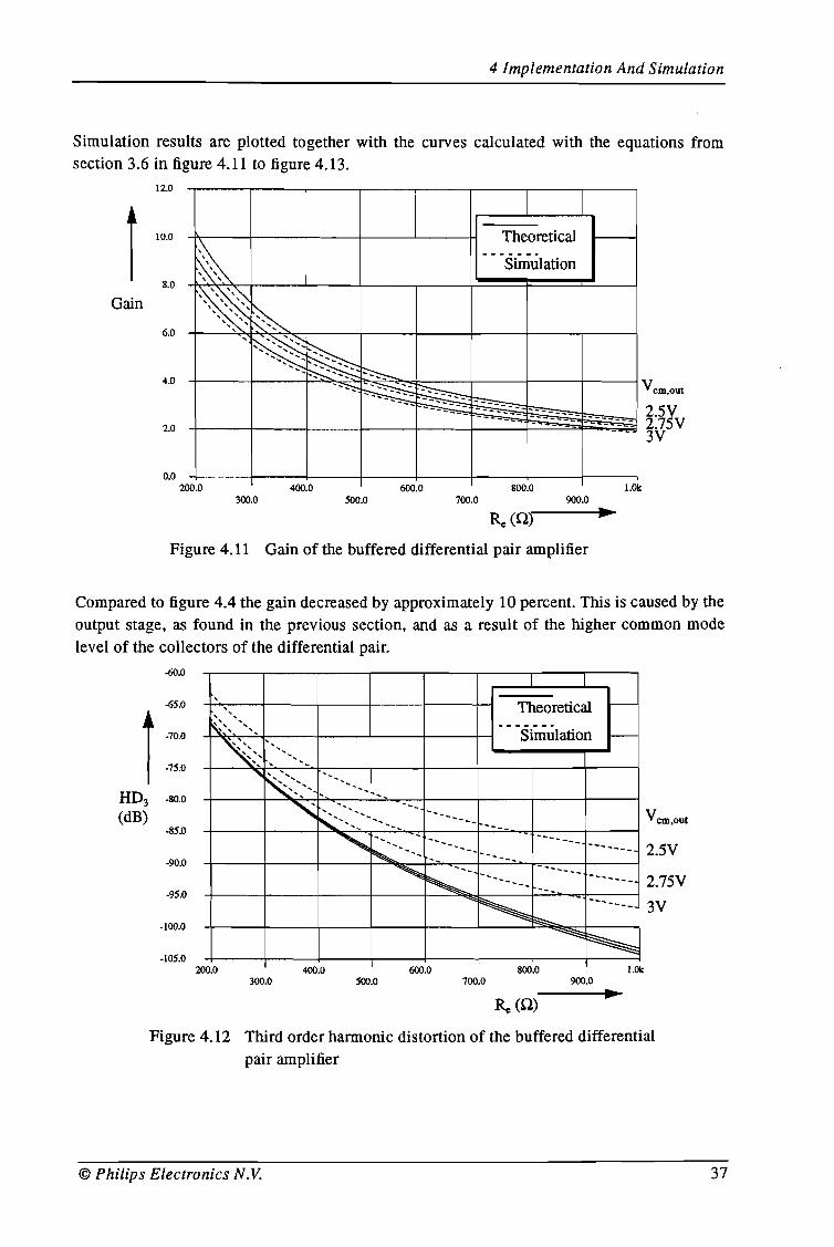
Simulation results are plotted together with the curves calculated with the equations fromsection 3.6 in figure 4.11 to figure 4.13.
Theoretical
~_.--_.-
Simulation
.~~
, , ', ,, ,' ... , ...
'~~, -
-'-~-'-- ~--~
~~~~~:::: ---::::::.:."':"----
12.0
r10.0
8.0
Gain
6.0
4.0
2.0
0.0200.0 400.0 600.0 800.0 l.Ok
Vcm,out
2.5V2.75V3V
300.0 500.0 700.0 900.0
Figure 4.11 Gain of the buffered differential pair amplifier
Compared to figure 4.4 the gain decreased by approximately 10 percent. This is caused by theoutput stage, as found in the previous section, and as a result of the higher common modelevel of the collectors of the differential pair.
2.5V
Vcm,out
I--
------.
I
Theoretical-------
Simulation
~" -" -" -...... ... ......... .. ...
~~::::- ,,------ ----._-. ----
, ," .......~ .. '" "I~,'" ......
·95.0
-90.0
-105.0
-100.0
-60.0
-65.0
1-10.0
-75.0
HD3 -80.0
(dB)-85.0
200.0 400.0 600.0 800.0 l.Ok300.0 500.0 100.0 900.0
Re (0)
Figure 4.12 Third order harmonic distortion of the buffered differentialpair amplifier
© Philips Electronics N.V. 37
4 Implementation And Simulation
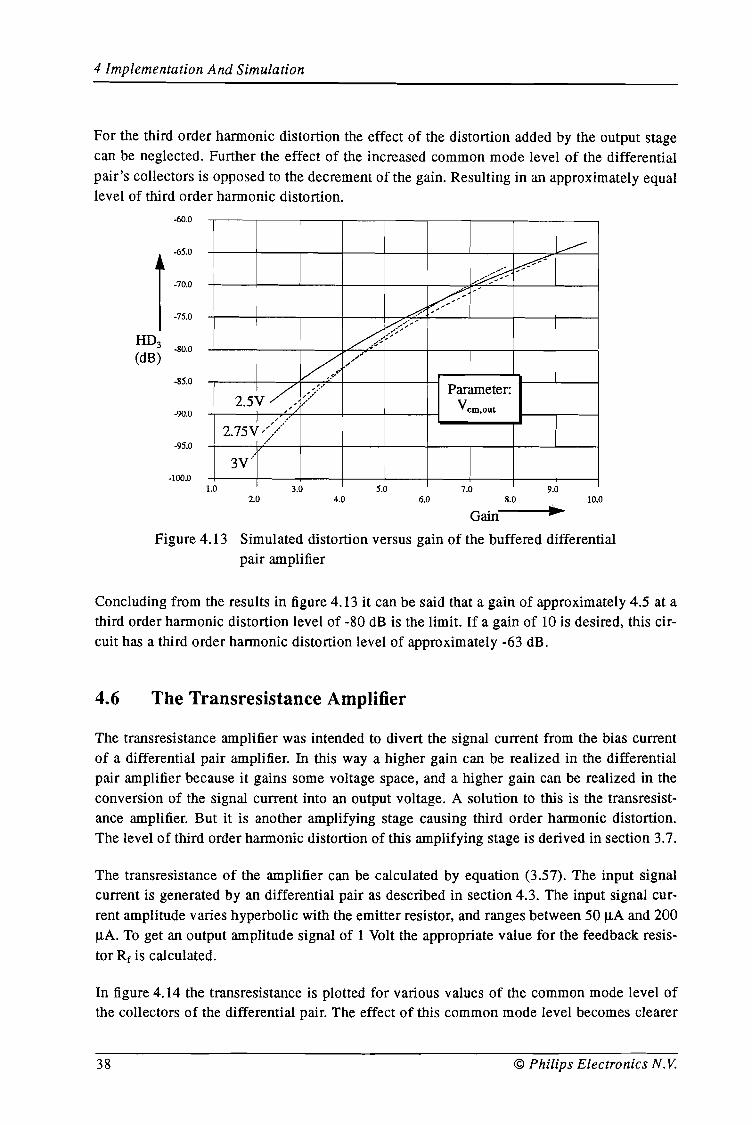
For the third order harmonic distortion the effect of the distortion added by the output stagecan be neglected. Further the effect of the increased common mode level of the differential
pair's collectors is opposed to the decrement of the gain. Resulting in an approximately equallevel of third order harmonic distortion.
-60.0
1-65.0
-70.0
·75.0
HD3 -80.0(dB)
-85.0
-90.0
-95.0
-100.01.0
/. '.''.'2.5V ,.~.~/
" ."I , ••'
3.02.0 4.0
5.06.0
Parameter:Vern,out
7.08.0
9.010.0
Figure 4.13
Gain
Simulated distortion versus gain of the buffered differentialpair amplifier
Concluding from the results in figure 4.13 it can be said that a gain of approximately 4.5 at athird order harmonic distortion level of -80 dB is the limit. If a gain of 10 is desired, this circuit has a third order harmonic distortion level of approximately -63 dB.
4.6 The Transresistance Amplifier
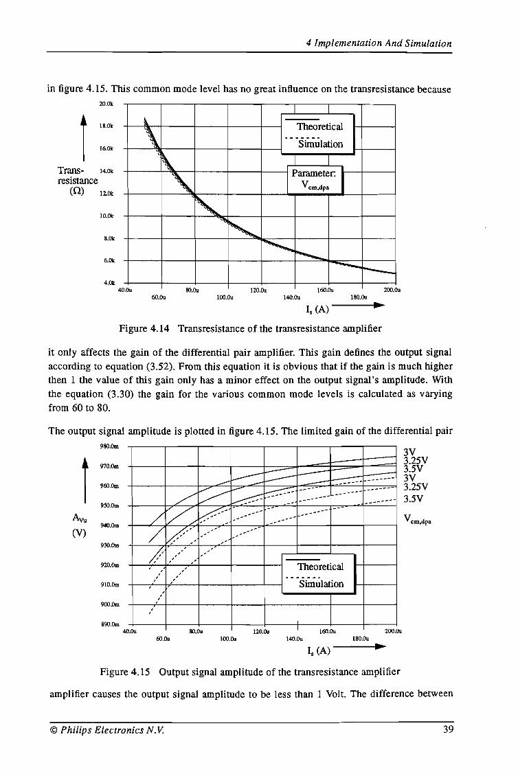
The transresistance amplifier was intended to divert the signal current from the bias currentof a differential pair amplifier. In this way a higher gain can be realized in the differentialpair amplifier because it gains some voltage space, and a higher gain can be realized in theconversion of the signal current into an output voltage. A solution to this is the transresistance amplifier. But it is another amplifying stage causing third order harmonic distortion.The level of third order harmonic distortion of this amplifying stage is derived in section 3.7.
The transresistance of the amplifier can be calculated by equation (3.57). The input signalcurrent is generated by an differential pair as described in section 4.3. The input signal cur
rent amplitude varies hyperbolic with the emitter resistor, and ranges between 50 IlA and 200~A. To get an output amplitude signal of 1 Volt the appropriate value for the feedback resistor Rf is calculated.
In figure 4.14 the transresistance is plotted for various values of the common mode level ofthe collectors of the differential pair. The effect of this common mode level becomes clearer
38 © Philips Electronics N. V.
4 Implementation And Simulation
ZOO.aul60.aulZO.OuSO.au
~ Theoretical\\ -------Simulation
\\\Parameter:"
Vcm.dpa
~."'l!
"-~~ ----r---
4.0k4O.au
6.0k
l6.0k
lS.Ok
S.Ok
lO.Ok
Trans- l4.0k
resistance(0.) l2.0k
in figure 4.15. This common mode level has no great influence on the transresistance because2O.0k
6O.au lOO.au l40.au lSO.au
Figure 4.14 Transresistance of the transresistance amplifier
it only affects the gain of the differential pair amplifier. This gain defines the output signal
according to equation (3.52). From this equation it is obvious that if the gain is much higherthen 1 the value of this gain only has a minor effect on the output signal's amplitude. With
the equation (3.30) the gain for the various common mode levels is calculated as varyingfrom 60 to 80.
The output signal amplitude is plotted in figure 4.15. The limited gain of the differential pair
-l---:::::-~~ -.....- --~ -------
/ v ~------ -------
~.. ------
~ ... ------- ----------- ---//V-' - -- ---
/_.. --- --------,- ......... ----- ,
/ V", -, ... ..,. ... -" ...--- .-- - .-
/ , , ,-, , --,, ,,Theoretical, , , ,, -, ,, -------, , Simulation, ,
,,,,,
9SO.Om
r970.Om
960.Om
950.Om
Avu940.Om
(V)930.Om
9ZO.Om
9l0.Om
900.Om
S90.Om4O.au SO.au l20.Ou l60.au 200.au
3V3.25V3.5V3V3.25V3.5V
Vcm.dpa
6O.au lOO.au l40.au ISO.au
Figure 4.15 Output signal amplitude of the transresistance amplifier
amplifier causes the output signal amplitude to be less than 1 Volt. The difference between
© Philips Electronics N.V. 39
4 Implementation And Simulation
the theoretical curves and the simulation results can be explained with the fact that the inputimpedance of the differential pair is finite. This causes a part of the signal current to flow intothe bases of the differential pair's transistors, resulting in a lower output signal amplitude.
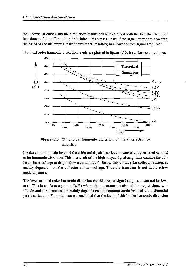
The third order harmonic distortion levels are plotted in figure 4.16. It can be seen that lower-
,, I, ,," , Theoretical -~~" -------
,<- Simulation'"
c---
~"
......:: ;;.."'" "'-- ..."-~
",~r=:::-- -------
t:---------- -------' ....,~'::: .....
I'--- ...... -:: :::-----r---""- ---
-........ --, -- --- ...-, -',
~ --I---I---"- --------- --..... -r---r--r----
-62.0
I -64.0
-66.0
HD3 -68.0
(dB)-70.0
-72.0
-74.0
-76.0
-78.040.00
60.0080.00
100.00120.00
140.00160.00
180.00
~
Vcm,dpa
3.5V3.5V3.25V3V
3.25V
3V200.00
Figure 4.16 Third order harmonic distortion of the transresistanceamplifier
ing the common mode level of the differential pair's collectors causes a higher level of thirdorder harmonic distortion. This is a result of the high output signal amplitude causing the collector base voltage to drop below a certain level. Below this voltage the collector current ismainly dependent on the collector emitter voltage. Thus the transistor is not in its activemode anymore.
The level of third order harmonic distortion for this output signal amplitude can not be lowered. This is conform equation (3.59) where the numerator consists of the output signal amplitude and the denominator mainly depends on the common mode level of the differentialpair's collectors. From this can be concluded that the level of third order harmonic distortion
40 © Philips Electronics N. V.
4 Implementation And Simulation
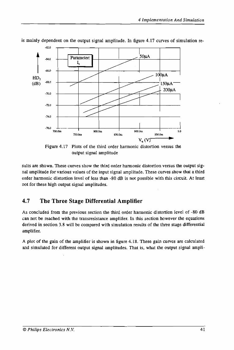
is mainly dependent on the output signal amplitude. In figure 4.17 curves of simulation re--62.0
r-64.0
-66.0
HD3
(dB) -68.0
-70.0
-72.0
-74.0
~150~Parameter:Is
~~
~......-
~lOP~A
---/ ~ ~150~-
~ ---___ 200~
~~
~~
~
~~
-76.0700.Om
7S0.OmSOO.Om
8S0.Om900.Om
9S0.Om1.0
Figure 4.17Vu (V)
Plots of the third order harmonic distortion versus theoutput signal amplitude
suits are shown. These curves show the third order harmonic distortion versus the output signal amplitude for various values of the input signal amplitude. These curves show that a thirdorder harmonic distortion level of less than -80 dB is not possible with this circuit. At leastnot for these high output signal amplitudes.
4.7 The Three Stage Differential Amplifier
As concluded from the previous section the third order harmonic distortion level of -80 dBcan not be reached with the transresistance amplifier. In this section however the equationsderived in section 3.8 will be compared with simulation results of the three stage differentialamplifier.
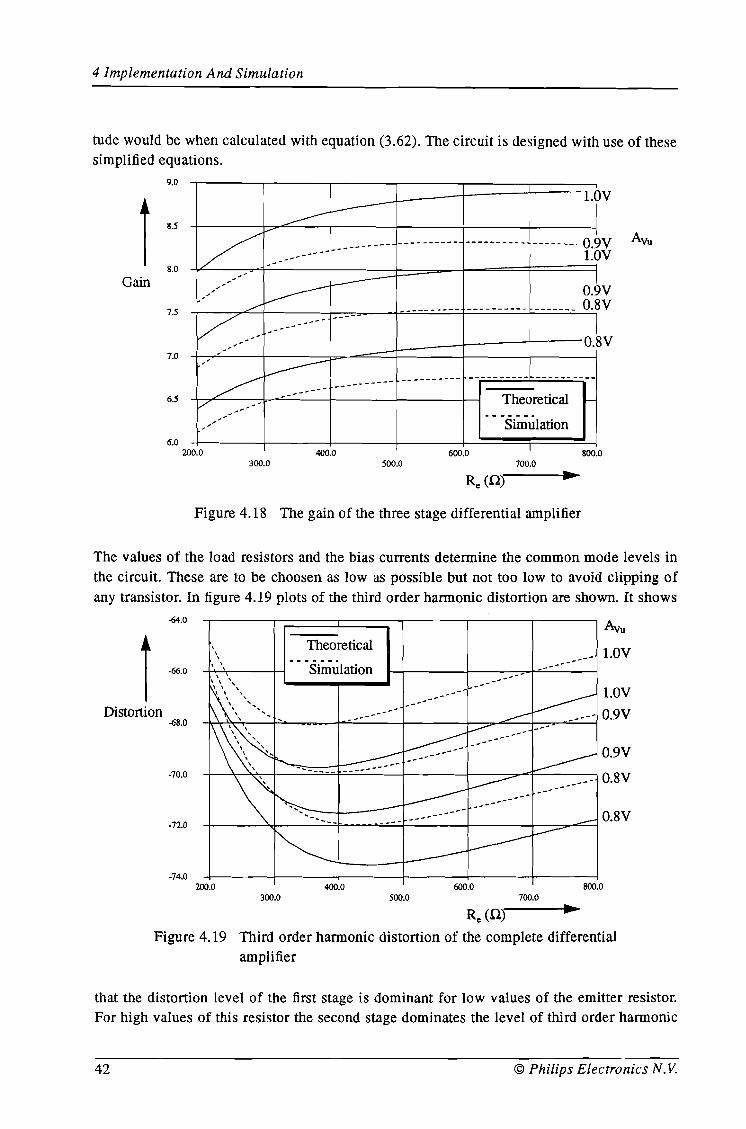
A plot of the gain of the amplifier is shown in figure 4.18. These gain curves are calculatedand simulated for different output signal amplitudes. That is, what the output signal ampli-
© Philips Electronics N. V. 41
4 Implementation And Simulation
tude would be when calculated with equation (3.62). The circuit is designed with use of thesesimplified equations.
- • -SiID~lation
9.0
I 8.5
8.0
Gain
7.5
7.0
6.5
-L--+--i--l.OY
-----~ I
~~--,-" ..._.._.._--- ---------- ---------- -------. ?:g~
,///~~ o.by~ O.8Y
~ " ..--." ..-.-- I/,/" O.8Y
" ~~ , ..-'_...,.------- -------- ---------- ----------
v Theoretical f-
".,. ... ""' ....
"
Avu
6.0200.0
300.0400.0
500.0600.0 I
700.0800.0
Figure 4.18 The gain of the three stage differential amplifier
The values of the load resistors and the bias currents detennine the common mode levels inthe circuit. These are to be choosen as low as possible but not too low to avoid clipping ofany transistor. In figure 4.19 plots of the third order hannonic distortion are shown. It shows
'-Ir==:C===lT--i-i-i Avu-64.0
Distortion-68.0
-70.0
-72.0
-74.0
\\
\
\ "
200.0300.0
Theoretical-_.-.--
Simulation
400.0
,,'.-'.,-
,,',-'
-"-----
600.0500.0
",,,'
,,'
,,',-'
,,'.,-
700.0
.-- l.OY
800.0
Figure 4.19
Re(n)
Third order hannonic distortion of the complete differentialamplifier
that the distortion level of the first stage is dominant for low values of the emitter resistor.For high values of this resistor the second stage dominates the level of third order harmonic
42 © Philips Electronics N. V.
4 Implementation And Simulation
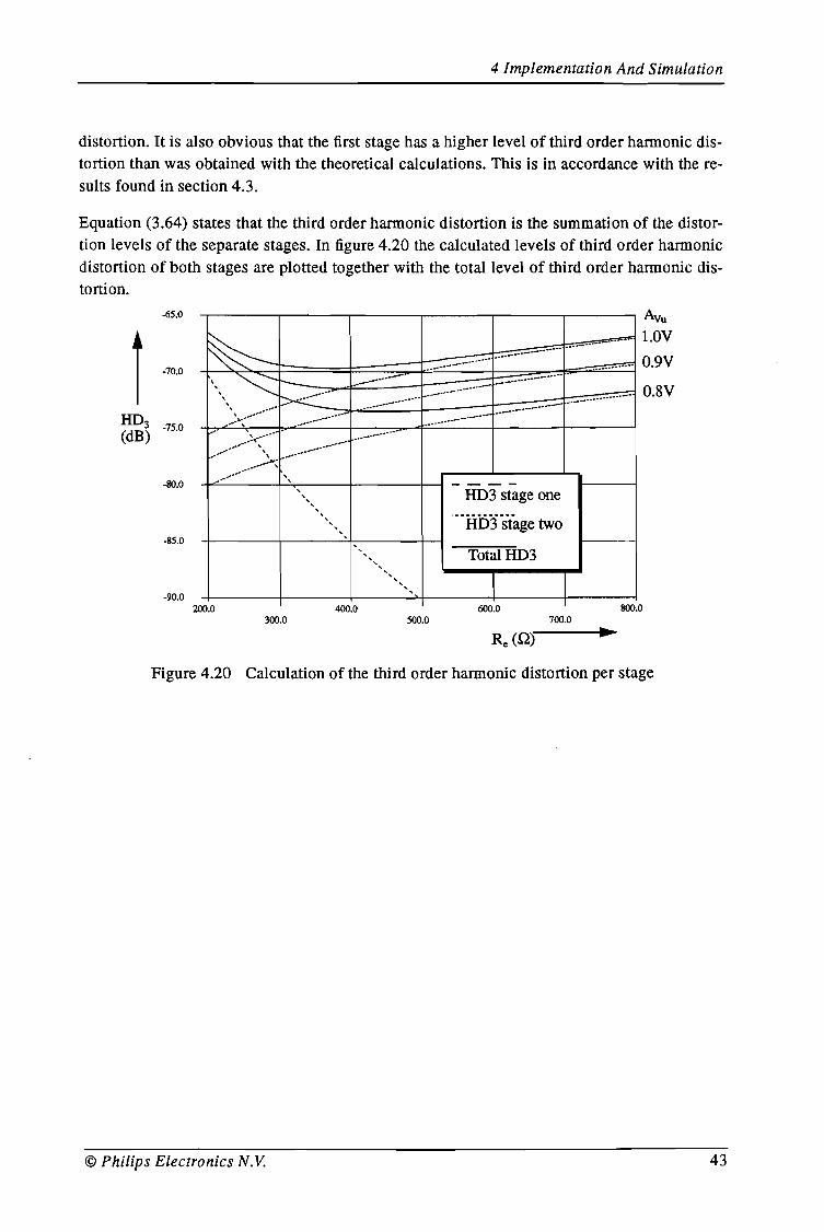
distortion. It is also obvious that the first stage has a higher level of third order hannonic distortion than was obtained with the theoretical calculations. This is in accordance with the results found in section 4.3.
Equation (3.64) states that the third order hannonic distortion is the summation of the distortion levels of the separate stages. In figure 4.20 the calculated levels of third order hannonicdistortion of both stages are plotted together with the total level of third order hannonic distortion.
...----- -.. .. ..--_..- -....--..- - -
--..-- _ --..-..-.-.---_...- .t
HD3(dB)
-65.0
.70.0
·75.0
·80.0
-.-----,-------,-------r-----,----.,.-------, Avu
.................= 1.0Y
....-.._......•.::::1::::".....-....-..... 0 9Y
...--........ ._ = 0.8Y
·85.0
,, , ,,,,,
,, ,, , , , , , ,
HD3 stage one
"-H03s'tage two
TotalHD3
·90.0200.0
300.0400.0
500.0600.0
I
700.0800.0
Figure 4.20 Calculation of the third order hannonic distortion per stage
© Philips Electronics N.V. 43
4 Implementation And Simulation
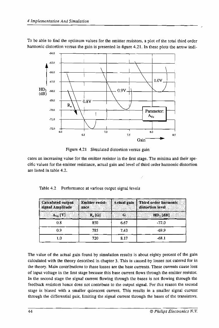
To be able to find the optimum values for the emitter resistors, a plot of the total third orderharmonic distortion versus the gain is presented in figure 4.21. In these plots the arrow indi-
-64.0
r-65.0
-66.0
-67.0
-68.0
-69.0
-70.0
-71.0
-72.0
\
\ \\ \ \ l.OV
\ \ "")
'"\\O.8V
\ O.9V
Re\ \ ~/
'\Parameter: r----
Avu
~J6.0
6.57.0
7.58.0
8.5
Gain
Figure 4.21 Simulated distortion versus gain
cates an increasing value for the emitter resistor in the first stage. The minima and their specific values for the emitter resistance, actual gain and level of third order harmonic distortionare listed in table 4.2.
Table 4.2 Performance at various output signal levels
-72.06.67
TllirdQrtt~J'·h~tlll~Iii~ •••••••·•· •••••••) }>}CI····~t~rtiql(l~Y~L} ••••• ?···.•·«····
8500.8
•••·.Q~i~ril~(~tltl~tp.J1tU •••••• sj~ij~~itim-P~i~ijtl~
0.9 785 7.43 -69.9
1.0 720 8.17 -68.1
The value of the actual gain found by simulation results is about eighty percent of the gaincalculated with the theory described in chapter 3. This is caused by losses not catered for inthe theory. Main contributions to these losses are the base currents. These currents cause lossof input voltage in the first stage because this base current flows through the emitter resistor.In the second stage the signal current flowing through the bases is not flowing through thefeedback resistors hence does not contribute to the output signal. For this reason the secondstage is biased with a smaller quiescent current. This results in a smaller signal currentthrough the differential pair, limiting the signal current through the bases of the transistors.
44 © Philips Electronics N. V.
4 Implementation And Simulation
Other loss factors are the parasitic resistors in the transistors causing extra voltage drops. Themost important of these are the emitter resistance because these conduct larger currents.
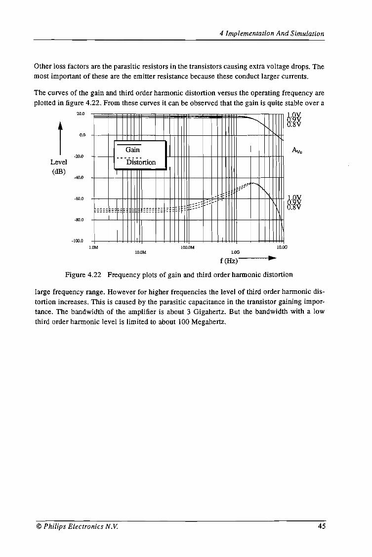
The curves of the gain and third order harmonic distortion versus the operating frequency areplotted in figure 4.22. From these curves it can be observed that the gain is quite stable over a
20.0
8:~~
r......
"0.0
Gain Avu-20.0 _.---.-
Level Distortion(dB)
-40.0
-60.0
-80.0
-100.0
==== == = 1==
1.0M
===: :: : --
1O.0M100.OM
LOG10.00
f(Hz)
Figure 4.22 Frequency plots of gain and third order harmonic distortion
large frequency range. However for higher frequencies the level of third order harmonic dis~
tortion increases. This is caused by the parasitic capacitance in the transistor gaining importance. The bandwidth of the amplifier is about 3 Gigahertz. But the bandwidth with a lowthird order harmonic level is limited to about 100 Megahertz.
© Philips Electronics N.V. 45
4 Implementation And Simulation
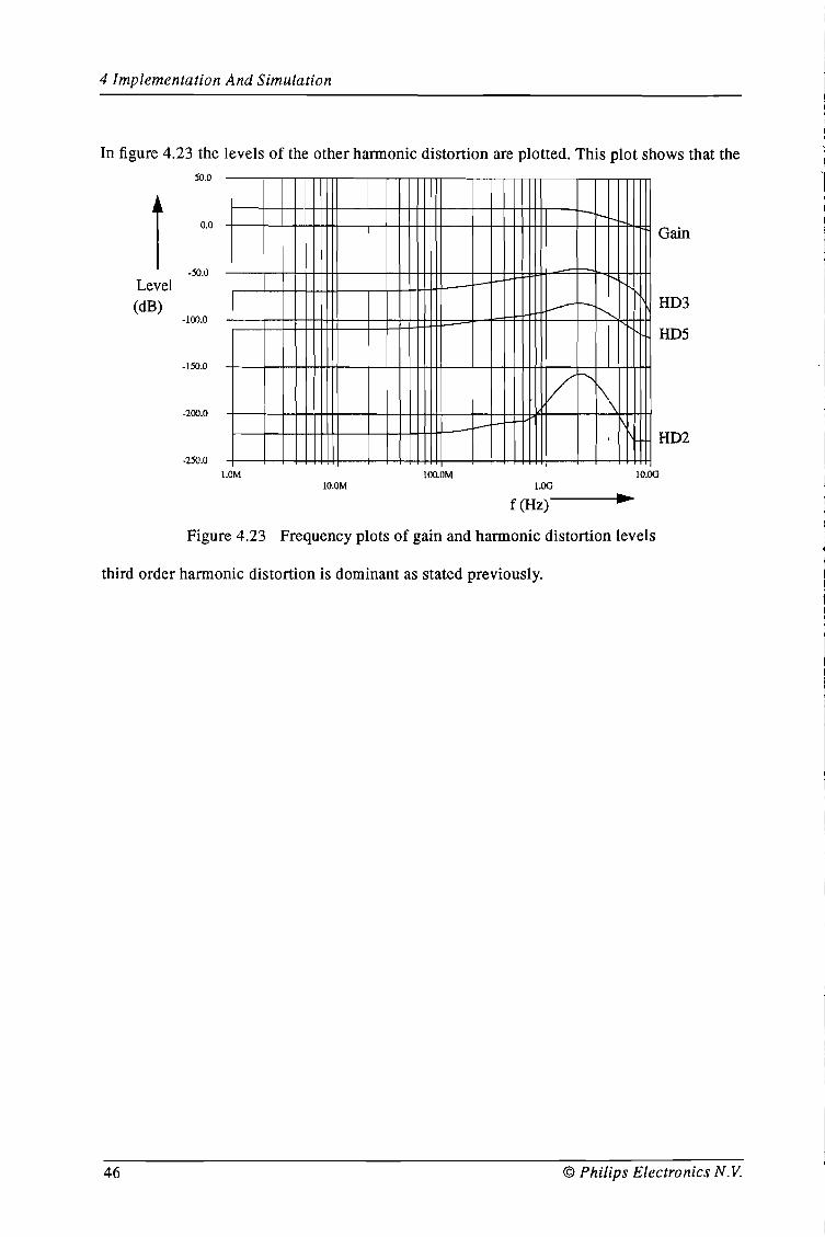
In figure 4.23 the levels of the other harmonic distortion are plotted. This plot shows that the50.0
I 0.0
-50.0Level(dB)
-100.0
-150.0
-200.0
-250.0
1'-1-
- ----r--
'" ,
V ~
1\1\
l-f-
Gain
HD3
HD5
HD2
l.OM10.0M
lOO.OM1.00
f(Hz)
10.00
Figure 4.23 Frequency plots of gain and harmonic distortion levels
third order harmonic distortion is dominant as stated previously.
46 © Philips Electronics N. V.
5 Conclusions And Recommendations
5 Conclusions And Recommendations
From the simulation results it can be concluded that the theoretical analysis of the circuitscan be used to do coarse calculations. The equations however can only be used if the transistor is kept in the active mode of operation. This implies some boundary conditions for the useof these equations.
Further it can be concluded that the circuits discussed in this report do not meet the specifications. For a distortion level as low as -80 dB the output signal amplitude of 1 volt can not bereached. For this output signal amplitude a distortion level of approximately -65 dB is minimal with the threestage amplifier discussed in section 4.7. With a distortion level of -80 dBan output signal amplitude of 450 millivolt is the best result. Conclusive it can be said thatthe distortion level is mainly dependent on the output signal amplitude.
The required bandwidth is not a limit on the circuits discussed.
Other amplifier principles could be tried. The following principles have been tested vaguely:
• An amplifier consisting of two buffered differential pair amplifiers with an overall feedback loop: This caused some instability at high frequencies.
• An equiripple design: This required a large number of differential pairs. To get a distortionlevel of -60 dB 25 differential pairs were needed!
Deeper analysis of these principles could lead to an amplifier with better performance.
© Philips Electronics N.V. 47
6 Acknowledgement
6 Acknowledgement
The graduation project was performed at the Philips Research Laboratories in Eindhoven.This graduation project was a part of a project of Integrated Transceivers, Group Brandsma.
I would like to thank Prof.dr.ir. R.J. van de Plassche for the opportunity of doing this projectand for his support during the project.
I also wish to thank all members of Group Brandsma and the neighbouring Group Woudawho have been a help for me in any possible way.
Eindhoven, May 1995,
L.P. de Goey.
© Philips Electronics N.V. 49
Appendix A Bibliography
Appendix A Bibliography
[1] Lieshout, P.J.G. van'Design of a bipolar Variable Gain Amplifier with a high gain range and low distorion'Afstudeerverslag TOO, June 1994.
[2] Gray, P.R and R.G. Meyer,'Analysis and Design of Analog Integrated Circuits'Second edition. New York: Wiley, 1984.
[3] Davidse, J.,,Analoge signaalbewerkingstechniek'Delft: Delftse Uitgeversmaatschappy, 1991.
[4] Sansen, W.M.C. and RG. Meyer,'Distortion in Bipolar Transistor Variable Gain Amplifiers'IEEE Journal of solid-state circuits, voI.SC-8, pp.275-282, August 1973.
[5] Davis, W.R. and J.E. Solomon,'A High-performance Monolithic IF Amplifier Incorporating Electronic Gaincontrol'IEEE Journal of solid-state circuits, voI.SC-3, ppA08-416, December 1968.
[6] Cherry, E.M. and D.E. Hooper,'Amplifing devices and low-pass amplifier design'Wiley, New York 1968.
[7] Stikvoort, E.F.'SAW-filter driver for TV tuners'Philips Nat.Lab., Technical note 050/93
[8] Stikvoort, E.F.'Mixer-output amplifier for TV tuners'Philips Nat.Lab., Technical note 084/93
[9] Meyer, RG. and W.D. Mack,'A DC to I-GHz Differential Monolithic Variable Gain Amplifier'IEEE Journal of solid-state circuits, vo1.26, no.lI, pp.1673-1680, November 1991.
[10] 'QuBiCl design manual',Philips components, February 1992.
© Philips Electronics N.V. 51
Appendix B Distortion Calculus
Appendix B Distortion Calculus
Distortion is a result of any non-linearities in the system transfer function. Here the equationsfor the harmonic distortion will be derived.
The distortion of the system depicted in figure B.! will be discussed.
X-----lNon linear system
y=f(x)I----y
Figure B.! A non-linear system
In order to find an expression for the harmonic distortion the transfer function y=f(x) can beexpressed in a Series of x with the Taylor-McLaurin theorem. This results in an approximation of y around a fixed point xo.
Y = Lan (x - xo)nn=O
Where the coefficients can be calculated with:
1 dn Ia = --y(x)
n n!dxx = Xo
For our nonlinear system the transfer function y=f(x) can be expressed as:
(8.1)
(8.2)
(8.3)
The higher order terms have been neglected because their contribution to the final expressionis assumed minimal.If a single tone signal is applied to this system with an amplitude A and a frequency f this results in:
From equation (B.4) can be seen that a nonlinear system is fed with a tone signal it also generates tone signal with frequencies which are a multiples of the original tone frequency.These are called higher order harmonics. The harmonic distortion is defined as the amplitude
© Philips Electronics N.V. 53
Appendix B Distortion Calculus
of this higher order harmonic relative to the amplitude of the first harmonic.The second order harmonic distortion can be expressed as:
(B.5)
The higher order terms can be neglected if the amplitudes are kept low. This simplifies theequation to:
(B.6)
In a similar wayan expression for the third order harmonic distortion can be derived.
54
(B.7)
© Philips Electronics N. V.
Appendix C Cascading Stages
Appendix C Cascading Stages
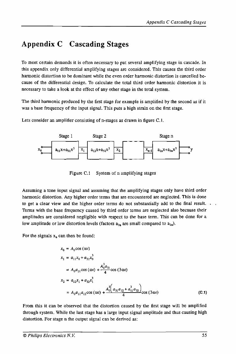
To meet certain demands it is often necessary to put several amplifying stage in cascade. In
this appendix only differential amplifying stages are considered. This causes the third order
harmonic distortion to be dominant while the even order harmonic distortion is cancelled be
cause of the differential design. To calculate the total third order harmonic distortion it is
necessary to take a look at the effect of any other stage in the total system.
The third harmonic produced by the first stage for example is amplified by the second as if it
was a base frequency of the input signal. This puts a high strain on the first stage.
Lets consider an amplifier consisting of n-stages as drawn in figure C.l.
Stage I Stage 2 Stage n
y
Figure C.I System of n amplifying stages
Assuming a tone input signal and assuming that the amplifying stages only have third order
harmonic distortion. Any higher order terms that are encountered are neglected. This is done
to get a clear view and the higher order terms do not substantially add to the final result. . .
Terms with the base frequency caused by third order terms are neglected also because their
amplitudes are considered negligible with respect to the base term. This can be done for a
low amplitude or low distortion levels (factors a3n are small compared to aln).
For the signals Xncan then be found:
Xo = Aocos (rot)
3AOa31= Aoau cos (rot) + -4-COS (3 rot)
3X2 = a12x I + a32x1
(C.1)
From this it can be observed that the distortion caused by the first stage will be amplified
through system. While the last stage has a large input signal amplitude and thus causing high
distortion. For stage n the output signal can be derived as:
© Philips Electronics N. V. 55
Appendix C Cascading Stages
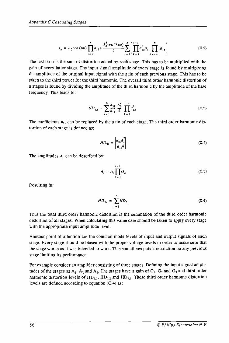
(C.2)
The last tenn is the sum of distortion added by each stage. This has to be multiplied with thegain of every latter stage. The input signal amplitude of every stage is found by multiplyingthe amplitude of the original input signal with the gain of each previous stage. This has to betaken to the third power for the third hannonic. The overall third order harmonic distortion ofn stages is found by dividing the amplitude of the third hannonic by the amplitude of the basefrequency. This leads to:
/I 2 i-I
~ a3i Ao II 2HD3/1 = £.J a."'4 au
i=1 1, k=1
(C.3)
The coefficients ain can be replaced by the gain of each stage. The third order hannonic distortion of each stage is defined as:
The amplitudes Ai can be described by:
i-I
Ai = AoIIGk
k=1
Resulting in:
/I
HD 3/1 = LHD3i
i = 1
(C.4)
(C.S)
(C.6)
Thus the total third order hannonic distortion is the summation of the third order hannonicdistortion of all stages. When calculating this value care should be taken to apply every stagewith the appropriate input amplitude level.
Another point of attention are the common mode levels of input and output signals of eachstage. Every stage should be biased with the proper voltage levels in order to make sure thatthe stage works as it was intended to work. This sometimes puts a restriction on any previousstage limiting its perfonnance.
For example consider an amplifier consisting of three stages. Defining the input signal amplitudes of the stages as AI' A2 and A 3• The stages have a gain of 0 1, O2 and 0 3 and third orderharmonic distortion levels of HD3•1, HD3,2 and HD3•3• These third order harmonic distortionlevels are defined according to equation (CA) as:
56 © Philips Electronics N. V.
Appendix C Cascading Stages
HD = la3.1A~13.1 a
l,14
2=HIA I. 2
HD 3•2 = H 2A2
2HD3•3 = H 3A3
Where Hi is characteristic for the third order harmonic distortion of each stage.
(C.7)
(C.S)
The amplitude of the input signal is Alt this results in an output signal amplitude of the firststage of AlGI' This equals the input signal amplitude of the second stage Az. Similar the input signal amplitude of the third stage can be found as AIGIGZ' and the output signal amplitude as A IGIGZG 3• This is in accordance with equation (C.5).
The third order harmonic distortion that is caused by each stage can be expressed as:
2HD3• 1 = HIA I
ZHD 3,2 = H 2 (A IGI )
ZHD3.3 = H3(AI Gl G2)
The third order harmonic distortion is the quotient of the amplitude of the third harmonic andthe base frequency. This quotient is not affected by any following stage because the first andthe third harmonic are amplified with the same gain. So the total level of third order harmonicdistortion of the cascade is the addition of all contributions of each stage as described inequation (C.8).
© Philips Electronics N.V.
2+ Hz (AI Gl )
2+ H 3 (A I GI G2)
(C.9)
57