
EIIIEIEEEEE EIIIIIIIIIIu I mhmmmhhmh · · 2014-09-2720 ABSTRACT ((',,,II , ,,rreer.,. -te It r-....
106
7A-A L0 3 5S a HU"S AIRCRAFT CO TORRANCE CALIF TORRANCE RESEARCH --ETC PilI 140 6HZ PUL.SED WNATT CONSINER HIGH POWER SOURCE. (U) UNCIJAN So T T FON T A IIDFORD. E N NAKAJI OAAKII-?-C-00AO UNCLASSIFIED HAC-W-AZSOS ARBRL-CR-00411$ NL I mhmmmhhmh EIIIEIEEEEE EIIIIIIIIIIu
Transcript of EIIIEIEEEEE EIIIIIIIIIIu I mhmmmhhmh · · 2014-09-2720 ABSTRACT ((',,,II , ,,rreer.,. -te It r-....

7A-A L0 3 5S a HU"S AIRCRAFT CO TORRANCE CALIF TORRANCE RESEARCH --ETC PilI140 6HZ PUL.SED WNATT CONSINER HIGH POWER SOURCE. (U)
UNCIJAN So T T FON T A IIDFORD. E N NAKAJI OAAKII-?-C-00AO
UNCLASSIFIED HAC-W-AZSOS ARBRL-CR-00411$ NL
I mhmmmhhmhEIIIEIEEEEEEIIIIIIIIIIu

LEVEL 1CONTRACT REPORT ARBRL-CR-00414
-V.'
140 GHz PULSED IMPATT COMBINER
HIGH POWER SOURCE
Prepared by
Hughes Aircraft CompanyTorrance Research Center
3100 W. Lomita Blvd.Torrance, CA 90509 /TICZ
S APR 2 JC I
January 1980 B
US ARMY ARMAMENT RESEARCH AND DEVELOPMENT COMMANDBALLISTIC RESEARCH LABORATORY
ABERDEEN PROVING GROUND, MARYLAND
Approved for public release; distribution unlimited.
0
Li-, 1
L, i • iQ

Destroy this report when it is no longer needed.
Do not return it to the originator.
Secondary distribution of this report by originatingor sponsoring activity is prohibited.
Additional copies of this report may be obtainedfrom the National Technical Information Service,U.S. Department of Commerce, Springfield, Virginia22151.
The findings in this report are not to be construed asan official Department of the Army position, unlessso designated by other authorized documents.

UNC'-. SS IFIE1)
SECURITY CLASSIFICATION OF THIS PAGE (W~hn Data Ent.red)
REPORT DOCUMENTATION PAGE BEFRE __ ISTRUTI____ ORM
I REPORT NUMBER 2. GOVT ACCESSION NO. 3 RECIPIENT'S CATALOG NUMBER
CO)NTRA\CT R11'ORT Ail KI.-CRI-0 0-14.
4 TITLE (nd Subtitle? 5 TYPE OF REPORT & PERIO- C O EREL:
140 GHz PULSED IMPATT COMBINER HIGH POWER FINAL REPORT
SOURCE6 PERFORMING ORG REPORT NLJMRFE 1
/ ,'/ - W-42585
7 AUTHOR(.I 8 CONTRACT OR GRANT NuMaEI-i--.
T. T. Fong E. M. Nakaji DAAK1l-77-C-0040
T. A. Midford Y. C. Ngan
9 PERFORMING ORGANIZATION NAMF AND ADDRESS 10 PROGRAM ELEMENT. PROJI J 7 1 A'
HUGHES AIRCRAFT COMPANY AREA 8 WORK UNIT NUMBI R
Torrance Research Center
3100 W. Lomita Blvd., Torrance, CA 90509
1 CONTROLLING OFFICE NAME AND ADDRESS 12 REPORT DATE
US Armv Ai'mIIllent Research :1nd PI'vcl pill t [(,IIIf:lltd1tIS ..\Im Ii:l I i st ic Research LIaboratory 1. NUMBER OF PAGES
(\ T.\ : 1IR1.AR- Ill) NUM9ERO AG E1
Ahcrdceln Prov inl (_ Ground . Md _10(05
14 MONITORING AGENCY NAME A ADDRESS(Ii dIf -Iro I ro1111IIIl6 01f1i 15 SE( URITY ( L ASS ot fh -p r,
UNCLASSIFIED
ISA. D CLASSIFICATON DOWN-,RA,-N-,S('R I fU L E
16 DISTRIBUTION STATEMENT (of thi.s Report)
.\pprlo\'ed for I1 )l i5 C ' ('c 1s2; d istr ibut ion tillI ji itcd.
17 DISTRIBUTION STATEMENT rof Ifh- t r e erd i,, 20,. it difer'nt fIro ep. t
IS SLIPPLEMENTARY NOTES
19 KF Y WORDS; 1C,,ottn-e ot. -1,'rs Hel o-- -t( .€ ....I f ItV 1,, ltto, er
140 GHz IMPATT Diodes
Millimeter Wave Power Combining
Pulsed IMPATT Oscillators
IMPATT Diodes
20 ABSTRACT ((',,,II , ,,rreer.,. -te It r-. arv nIf ieI- h, h, blo, k,
The objective of this program was to develop silicon IMPATT diode and power
combiner circuit technology in order to demonstrate improved pulse power
generating capability at 140 Gtlz. The program efforts have led to significantadvances in the state-of-the-art for pulsed olid state power generation in
D-band.
'fhe diodes fabricated for this program were double drift IMPATTs with activeregions formed by a combination of n-type epltaxial growth and multiple
nnFORM 43 ET, O O 'OOLTDD I JAN73 1473 EDITION OF I NOV65 IS OBSOLETE UNCLASSIFIED
SECUIRITY CL ASSI ICAT ION OF TIllS P-Al f P , " . IrI

UNCLASSIFIEDSECURITY CLASSIFICATION OF THIS PAGE( oen Do(. Entered)
20. dose/energy p-type ion implants. Since the diodes were intended for
operation under short pulse ('v. 100 ns) conditions, copper heat sinkswere used.
Several diode package configurations were studied. The most successfulwas a double quartz standoff configuration.
Three types of power combining structures were investigated in detailduring the program. These included:
1) A resonant rectangular waveguide structure with center-mounted
diodes.
2) A variation of (1), employing the coplanar biasing configuration.
3) A rectangular waveguide combiner with sidewall-mounted diodes(Kurakowa circuit).
Of these three combiner circuits, the rectangular cavity with sidewallmounted diodes was by far the most successful. In this circuit, powerfrom two pulsed diodes was combined with approximately 90% combining
efficiency.
As a result of techniques developed during the program, high peak poweroutput at 140 GHz was achieved for both single and multiple diodeoscillators. As a result of improved diode design and fabrication,single diode peak power levels of 3.0 watts at 3% efficiency were obtainedfor a 100 ns pulse length and a 50 KHz pulse repetition frequency. Thisrepresents an approximate factor of four increase in single device powerduring the program. In addition, a two-diode power combiner based onan oversize version of Kurakowa circuit was constructed which produced3.0 watts of peak output power.
At the conclusion of the technical effort, two high power pulsed sourcescomplete with modulators were delivered to the Army. One of thesesources is a single diode oscillator, the other a two diode powercombiner oscillator. Both of these sources meet the program object of3.0 watts of peak output power at pulse lengths of 50-100 ns.
ILUNCLASSIFIED
SECURITY CLASSIFICATION OF THIS PAGE(Wh-, Ve F,,Ird)

FOR EWORD
This project (Contract No. DAAKII-77-C-0040) was initiated by the
U.S. Army Ballistic Research Laboratories. The project monitor was
Mr. Dick McGee (DRDAR-BLB). This report is a summation of the entire
program effort conducted from 1 July 1977 through November 30, 1978.
This report was submitted by the authors June 1979.
The work reported herein was carried out at the Hughes Aircraft Company
Torrance Research Center, Torrance, California under the direction of
K. P. Weller and T. A. Midford. Other principal contributors were
C. Chao, T. T. Fong, E. M. Nakaji and Y. C. Ngan. Technical assistance
was provided by F. C. Fischer, A. E. Martin, M. G. Padella, and
G. Watanabe.
rNe U n Soc~ion
, II ....t
iii

TABLE OF CONTENTS
Section Page
I. INTRODUCTION 1
II. IMPATT DIODE DEVELOPMENT 4
2.1 Diode Design 4
2.1.1 Doping Profile and Depletion LayerThickness 5
2.1.2 Thermal Design 122.1.3 Design Summary 17
2.2 Device Fabrication Technology 20
2.2.1 Standard Fabrication Procedure 202.2.1a Epitaxial Silicon Matcrial 222.2.1b Evaluation of Epitaxial Material 232.2.1c Ion Implantation 262.2.1d Low lemperature Diffusion 292.2.1e Substrate Thinning 312.2.1f Metallization 312.2.2 Modified Grid-Etch Thinning Process 32
2.3 Package Design and Fabrication 33
2.3.1 Package Design 332.3.1a Single Standoff Package 33
2.3.1b Double Standoff Package 372.3.1c Directly Contacted Diode 372.3.1d Quartz Ring Pedestal Package 37
III. COMBINER CIRCUIT DEVELOPMENT 42
3.1 Rectangular Waveguide Resonator with WallMounted Diodes 43
3.2 Rectangular Waveguide Power Combiner - Center-Mounted Diodes 48
3.3 Coplanar Biased Waveguide Power Combiner -
Center-Mounted Diodes 51
IV. PULSED DIODE AND COMBINER CHARACTERIZATION ANDPERFORMANCE 56
4.1 Thermal Characterization 564.2 Single Diode RF Characterization 57
V
TABLE OF CONTENTS (CONTINUED)
Section Page
4.2.1 Measurement Setup 57
4.2.2 Diode Lot Evaluation 57
4.3 Two Diode Combiner Characterization 63
V. PERFORMANCE OF DELIVERED UNITS 68
VI. CONCLUSIONS AND SUGGESTIONS FOR FUTURE WORK 76
Appendix
A OPERATION INSTRUCTIONS FOR THE 140 GHz SINGLE-DIODEIMPATT OSCILLATOR AND TWO-DIODE IMPATT COMBINER 79
I i st 'i butio I Ol i t 89}
Vi

LIST OF ILLUSTRATIONS
Figure Page
1 Double drift IMPATT structure 7
2 Calculated small-signal conductance, susceptanceand device Q as functions of frequency for 140 GHzpulsed double drift IMPATT diode. 8
3 Semi-infinite solid heated by periodic impulseheat source over a circular area. 14
4 Transient thermal resistance of a pulsed IMPATTdiode on a copper heat sink. 16
5 Total pulsed IMPATT diode thermal resistance
on a copper heat sink. 1R
6 Schematic diagram of silicon epitaxial reactor. 24
7 Details of gas flow controls for the epitaxial reactor. 24
8 Schematic of 300 kV ion implantation machine. 27
9 140 GHz double drift IMPATT profile. 28
10 Schematic of diffusion furnace. 30
11 Diode pillformed by modified grid etch technique. 34
12 Double standoff high power 140 GHz diode. 35
13 Single quartz stand-off packaged diode for 140 CHzpulsed source (200X). 36
14 Double standoff package with bias pin shown in
normal operating position. 38
15 Directly contacted diode with gold ball. 39
16 Low parasitic quartz ring pedestal package for
pulsed 140 CHz operation. 40
17 Power combiner using coaxial modules in a
waveguide resonator.
18 Equivalent circuit for coaxially-coupled
resonant power combiner. 46
19 Resonant circuit configuration.
vii

LIST OF ILLUSTRATIONS (CONTINUED)
Figure Page
20 Power combining using coaxial modules mountedin the center of a waveguide. 50
21 Coplanar biased circuit design. 52
22 Four-diode combiner circuit using coplanar biased
scheme designed for 140 GHz operation. 53
23 Scanning electron micrograph of the four-diodecombiner showing the bias wires and resonant caps. 53
24 140 CHz four-diode combiner circuit assembledwith an output isolator. 54
25 Bias-pin transformer waveguide circuit configuration. 61
26 A typical input current pulse (top trace) andvideo output pulse (bottom trace) for a high
power 140 GHz pulsed oscillator. 62
27 Operating characteristics of a high power pulseddiode from lot DDD54. 64
28(a) Video outputs of input current pulse (top) andrf output pulse (bottom) for diode DDD54C-3. 65
28(b) Video outputs of input current pulse (top)and rf output pulse (bottom) for diode DDD54B-8. 65
28(c) Video outputs of input current pulses (top two
traces) and rf output pulse (bottom) when bothdiodes DDD54C-3 and DDD54B-8 were turned on. 66
:I Pulsed 3.0 watt 140 GHz IMPATT oscillator
with isolator. 69
30 Single-diode pulse modulator. 70
-I Single diode oscillator and pulse modulator. 71
32 145 GHz Two-diode combiner. 72
13 Two-diode pulse modulator. 73
1' Pulsed two-diode combiner developed for 140 GHz
operation. 74
viii

I. INTRODUCTION
The objective of the work described in this report was to develop a
140-Cliz pulsed IMPATT diode power combiner high power source. Advanced
diode, packaging and combiner circuit technologies were developed and
implemented for this program which resulted in state-of-the-art results
for pulsed TMPATT diodes operating at 140 GHz and the first demonstration
of efficient pulsed power combining from more than one IMPATT diode
at frequencies above 100 GHz. The performance goals for the power com-
biner are summarized in Table I.
TABLE I
140 GHz PULSED POWER COMBINER COALS
Frequency 140 GHz
Peak power output 3 W
Pulse length 100 n sec
Additional technical goals of the program were: (1) to further develop
and refine 140 Gtlz IMPATT diode technology to the end of achieving the
reproducible fabrication of 1 watt peak power diodes, and (2) to demon-
strate the feasibility of adding power from two or more IMPATT diodes
It 140 CIlz.
The development efforts on this program were carried out in three major
areas: IMPATT diodes, diode packaging and power combiner circuits.The ujodes fabricated for the program were double drift region (DDR)
i .. . .. . _ , = 1

silicon IMPATTs with active regions formed by epitaxial growth and ion
implantation. Attempts were also made at fabricating diodes entirely
by multiple epitaxy, the performance of these diodes; however,was inferior
to that of the ion implanted structures. A semi-empirical design approach
was adopted which consists of successive iterations of a combination
of theoretical analysis and experimental results. At the end of the
program, the best performing diode lots had measured doping profiles
in good agreement with optimized design predictions. Because the devices
used on this program were operated at short pulse lengths (100 n sec)
and low duty cycle, copper heat sinks were used.
Several variations of IMPATT diode package were investigated. These
include single and double quartz standoff configurations as well as
the direct - contacted (packageless) diode and a low inductance pedistal
version of the standard Hughes quartz ring package. Of these, the double
quartz standoff package was by far the most sucessful. All of the high
power pulsed diodes developed during the program used this package.
The major millimeter wave power combiner circuits which were studied
during the program include: (1) a rectangular resonant waveguide cavity
employing center-mounted diodes, (2) an alternate version of (1), the
so-called "coplanar biased" waveguide combiner circuit, and (3) a rec-
tangular resonant waveguide combiner employing wall-mounted diodes.
The latter is the Kurakowa circuit used sucessfully at X-band with up
to 8 diodes. We have used a variation of the Kurakowa circuits to com-
:.':~e. power from two pulsed TMPATT operating near 140 GIlz with approxi-
7,,1v 90 combining efficiency.
i'i,. work described in this report has led to the achievement of some
..-V significant progress including a substantial advance in the state-
:'-toi-art performance of pulsed IMPATT diodes operating at 140 G1lz.
ifically we have achieved:
2

I. A peak output power of over 3.0 f from a s i ngle p, I , I.'A,"
diode operating at 140 CHz.
2. The first demonstration of highly efficient power cihing,
at 140 GlIz. Using two diodes in the Kurakowa typo ci rcuit,
we have fabricated a pulsed power cop-hint-r which ceneratc-s
3 watts of peak output power.
The performance objectives of this prozrrim haive thi,: ai b- u r- t or
exceeded.
At the conclusion of the technical effort, two pulsed solr-,s completI
with modulator were delivered to the Army. Both of these sources' met
the program goal of 3.0 watts of output power. One source was ; ci ag 1
diode pulsed oscillator operation at 140 GHz, the other a two diade
pulsed power combiner/oscillator operating near 145 Gliz.
In Section II of this report. the IMPATT diode design, fabrication
and packaging procedures are described. Section 11 deals with power
combiner circuit development. Section IV presents performance data
for the pulsed diodes and power combiner circuits. Section V summarics
the performance of the delivered hardware. Finally. Section VI presents
the conclusions and suggestions for future work. In App,-ndix A nddi-
rional spec fications and operating procedure: !-,I th e deliv,--,te hanr-
.-, provided.
II. IMPATT DIODE DEVELOPMENT
In this section, the technical approach used to develop pulsed IMPATT
diodes at 140 GHz is described. The procedure for the IMPATT diode
design is discussed in Section 2.1. The diode fabrication techniques
are described in Section 2.2. Section 2.3 deals with diode package
design and fabrication.
2.1 DIODE DESIGN
The key parameters involved in the design of IMPATT diodes are the dop-
ing profile, epitaxial-region thickness, diode area and the thermal
resistance. A semi-empirical approach was used to determine the opti-
mum values for these parameters. In some cases, theoretical device
models were used to determine the initial design parameters. However.
these models are limited due to the many physical approximation required
to make practical calculation. 1 ,2 There are also basic limitations
due to the unavailability of certain fundamental material parameters.
Therefore, a design procedure based on an approximate theoretical analy-
sis and experimental data was used. This semi-empirical approach has
resulted in the achievement of state-of-the-art results for pulsed diodes
at 140 GHz.
To achieve maximum peak power output at 140 Glz, we have concentrated
on developing double drift TMPATT dindes with optimum doping profile
ind expitaxial layer thickness for pulsed operation. The double drift
diode has been chosen as our approach because of its established hi 0h
power and efficiency capabilities, as well as its high device impedance
for easier circuit matching to achieve optimum performance. The pulsed
diode, however, operates at much higher current densities than the CW
diode, its design is quite different and must be considered separately.
Another unique property of the pulsed IMPATT diode is that the operating
'-4

frequency chirps across the bias pulse becaui, , (,f the tlmt ( ' i~i -tit I ml, :.
tion during the pulse. This frequency chirp charactori tlc i ; 1,ttn
used in a radar system to improve the glint and clutter r,,ct i, ,
Ls therefore an important property. In the following L t pl pu4,d di
design and thermal considerations are sutn-narized. B13.id on tit , con-
siderations, a summary set of device paramete rs is then pr,.S,,nt u-
140 (I-Iz pulsed operation.
2.1.1 Doping Profile and Depletion Laver Thickness
For pulsed double drift IMPATT diodes, the primary, design conidornt Ion
is the impedance-frequency characteristic of the diode as n functio,
of current density. Because IMPATT operation is strongly current deptn-
dent, the frequency for peak negative conductance is a function o1 the
operating current. As current density increased, the optimum froquency
increases and so does the diode output power. For C diodes the maximumrl
current density is limited thermally, but for pulsed diodes this limit
is extended many times depending on the pulse width and duty factor.
For extremely narrow pulse widths and low duty operation, the diode is
no longer thermally limited. The current density can be further extended
until space charge effects cause power saturation 3nd officiency reductiT .
In other words the ultimate diode output power is limited electronicaliv.
To design a puL1sed diode, it is necessary to predotcrmin the operatin.,
current densitv. However, the operating current dens itv is also inti-
maly Ivdependent on several other factors, such as wu me 'idth, dut%
actor, power o(Itput and devic i'impedance. T chiiic ot -Ill optimurm
curront donsi tv must therefure hL e derived from colt ii tLlaI(1- f s al1d
the opt imization of a: set ,I pnra ters oil :iii,,iv;lI . ;I., on
lt.nild t rnnsient tLhi-ial IrtaIvsi , )I A 1i,' ,I , l "' I.
I v-.att p 'r dind , Ip w, r I' veI. , 1o l i pi -,, , _
I Am ip ,'cM' is ;tpp ropr ialto . I'I: ' t 1:t' 1t~ 1 , ' 1 , .; : ",,
Iazi i ... . i .. mp cc i.. .. P i l1 i i t i i i I 1 17 i -. . .. ... -i iI ii i
assuming a maximum junction temperature of 250 C. With a given operat-
ing current density and junction temperature, the diode doping profile
can then be designed.
The profile design is based on a symmetrical double drift region struc-
ture as shown in Figure I . The structure has equal doping densities
in tle n and p regions. It has been established both theoretically
and empirically that the symmetrical DDR diodes are capable of nearly
optimum performance in terms of output power and efficiency. The asym-
metricaly design which compensates the unequal ionization rates of elec-
trons and holes results in very minor improvement in the device perform-
ance. On the other hand, an optimum asymmetrical design requires a
full knowledge of the large signal behavior of the DDR diode which is
strongly circuit dependent. It is therefore difficult to ascertain
the optimum device parameters. More importantly, the minor improvement
that can be gained from an asymnetrical design, can be easily lost through
complication in epi growth or uncertainties in the design parameters,
such as field and temperature dependence of the electron and hole ioni-
zation rates. We therefore have followed the proven approach and designed
the DDR diodes around a symmetrical doping profile for which NA = ND .
For a given optimum current density and a maximum operating junction
temperature, the small signal device admittance can be calculated for
a given doping concentration. Strictly speaking, optimum diode design
,oquires knowledge of the large signal characteristics of the device.
,o,'ch in turn is strongly dependent on the circuit parameters. Since
;in exact analysis and accurate prediction of the circuit response is
lea r1v impossible at D-band (110-170 Cllz) frequencies, we base the diode
design on tile small. signal characteristics, modifying the design appro-
priately to take account of large signal effects. An example of this
desin n approach follows.
L i i . . . . .... . i

DOUBLE-DRIFT G1OOA
P+ p IN NHOLES ELECTRONS
z0
0
L)
DISANC
AVL-CH
-iw
DISTANCE
Figure~ I DouiblIe dr i tt I~I\ ~

G,994
-760.00 - 30000 -1.70
SUSCEPTANCE
-80000 250.00- -1.80
+0
S-M4.00 15 20.00- -2.0
UA 2.0 100.00- o-7100
z r
-90.00 100.00 -2.0.
-92000 10.00 -2.30In .
120000 130000 140000 150000 1600.00 1700.00 1800.00
FRE8UENCY-HZ 1*10+8)
S r - Calculated smal]-signal conductance, .111c'p~ct u , \i'
0 IS fuinctions. of freque:ic,. for 140 C, GH; m s d Jb , !i'
I dIA i d Ld.

Figure 2 presents the calculated small signal device admittance a a
function of frequency for J = 1.2 x 10⁵ Amp/cm and T. = 250(C. The1 17 3doping concentration is selected to be NA = N = 4.5 x 10 atoms/cm
Tile device admittance is obtained from a computer simulation based on
the analysis ef Misawa. 3 ,4 The ionization rates of Grant 2 and the drift
velocities given by Canali et. al. were used in the calculation.
It is seen from Figure 2 that the peak negative conductance occurs at
150 GHz. However, when operating in the large signal condition for
optimum power and efficiency, the IMPATT negative conductance decreases
in magnitude to approximately half of its small signal value, the device
susceptance increases which causes a downward shift in operating fre-
quency. Taking into consideration large signal effects, and to some
degree based on experience, we select N = N = 4.5 x 10¹⁷ atoms/cm3
A Das a reasonable doping concentration for the 140 6Hz pulsed diode. At
this doping concentration, the diode has a reverse breakdown voltage at
room temperature of about 9.5 volts. At a current density of 1.2 x l05
2 0Amp/cm and 250 C junction temperature, the operating bias voltage
is 14.0 volts. The higher bias voltage is a result of temperature
rise at the junction and space charge resistance.
To complete the diode design, it is required to determine the depletion
region widths of the n and p layers. For the svmmetrical structure
under consideration, the widths of the two regions ae equal. it there-
fore suffices to consider one region only. The total depletion width
is simply twice the single layer width.
For optimum diode performance the epitaxial layer thickness must be
precisely controlled such that the active epi thickness is equal to
the total depletion width at the optimum operating current density and
maximum junction temperature. Under this condition the electric field
is bar,.ly punched through (punch through factor = 1). Further increas,
in the punch through factor causes widening in the avalanche zone width
9
which degrades the IMPATT efficiency and output power. On the other
hand epi that is too thick results in an unswept region which degrades
power and efficiency because of increased series resistance. To achieve
optimum performance, it is, therefore, important to determine the diode
depletion width at the operating current density and temperature. Since
the depletion width for a particular doping concentration at breakdown
and room temperature can be determined readily, it is necessary to consider
the depletion width widening caused by space charge and temperature
effects.
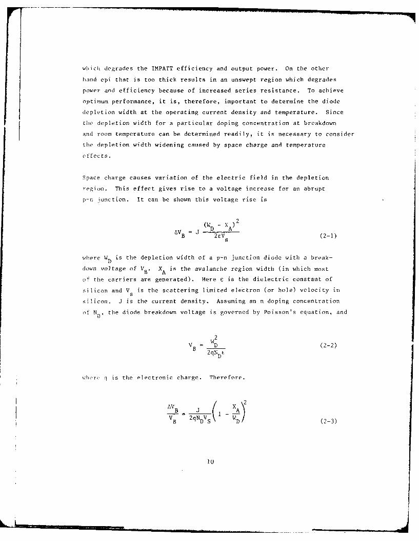
Space charge causes variation of the electric field in the depletion
region. This effect gives rise to a voltage increase for an abrupt
p-n junction. It can be shown this voltage rise is
(WD - XA )2
AVB = J 2EV (2-1)5
where WD is the depletion width of a p-n junction diode with a break-
down voltage of VB . XA is the avalanche region width (in which most
of the carriers are generated). Here E is the dielectric constant of
silicon and V is the scattering limited electron (or hole) velocity inS
silicon. J is the current density. Assuming an n doping concentration
of N ., the diode breakdown voltage is governed by Poisson's equation, and
2
V = D (2-2)2 qN E
wher(e q is the electronic charge. Therefore,
LV B _ -A
VB 2 qNDV S WD) (2-3)
10

The incremental depletion width, W D9 caused by the space charge can
now be obtained from
D B XA)
" VB 2qND sV S (2-4)
17 -3For N = 4.5 x 10 cm , X = 0.30 W for double drift diodes;
D 5A 2 D 6and letting J = 1.2 x 10⁵ Amp/cm and V = 8 x 10 cm/sec, we have
S
-- = 0.10 due to space chargeD
Thus, the depletion width is increased by about 10% due to space charge
effects.
The ionization rates of electrons and holes decrease with increasing
temperature. For an IMPATT diode with a given doping concentration
the depletion width (or breakdown voltage) will increase with increasing
temperature. The incremental depletion width caused by temperature
can be obtained by calculating the diode breakdown voltage at room tem-
perature and the operating temperature. For a junction temperature
0 17 - 3of 250°C and a doping concentration of ND = 4.5 x 10 cm , the voltage
rise in relation to V B at room temperature has been calculated using
a computer model and the rise is approximately 20%, or
AWD AV B
WD= V = 0.20 due to temperature riseD B
The total widening of the depletion region width is therefore 30%.17 -3For ND = 4.5 x 10 cm the total depletion width at breakdown and
11

,ioom temperature is 0.29 pm. At an operating temperature of 250C and5 2bias current density of 1.2 x 10 Amp/cm , the total depletion width
is
WT = 1.30 WD = 0.38 pm
For -a 140 0Hz pulsed double drift diode, the electron and hole regions
should therefore have a total depletion layer thickness of 0.38 Jim.
[i sumstary, the pulsed double drift IMPATT diode requires a lower doping
concentration as compared to the CW diode to compensate the much higher
operating current density. For 140 GHz operation we have determined
17 - 3that the doping density should be approximately 4.5 x 10 cm . The
high current density and elevated junction temperature also cause con-
slderable widening of the depletion layer. The increase in depletion
width is considerably larger in pulsed diodes; it therefore requires
,1 thicker epi layer than a CW diode. For 140 GHz operation, a total
:t,-ive layer width of 0.38 lpm is required.
?.1.2 Thermal Design
proper thermal design of pulsed IMPATT diode to achieve both high
a:., power and low junction temperature lies in the accurate prediction
7 Mnsient thermal properties of the diode, as it goes through periodic
i:i ca and cooling cycles caused by the bias pulses. Once the tr:nsi ,t
- m:l resistance is known, the maximum allowable bias input power
T, :aintain a safe operating junction temperature can be calcul ated.
, r, i red RF power in con junc t ion with the maximum input power then
,',,term ,s the device junction area and the operating curren density.
,, a first step, the transient thermal resistance of a diode must
rmined.
12

Consider now the case of a uniform heat source with radius R on a semi-
infinite heat sink of thermal conductivity K and thermal diffusivity
Oi as shown in Figure 3. It can be shown that the transient thermal
resistance related to the maximum temperature at the center of the diode
and at the end of a heating cycle is given by5
d/2 (at)/2 2 -R2/At+ 2Tt -K412 e
R R erf R(at12)/2 + + 1/2 (at1)/2 erfc It (2-5)
where
2 e - d x
j2
e u - e } p - cos _x2 1 cdx
(7t2)2)dx2(1 - e x
0
and d t I/t 2 is the duty factor (Figure 3). The first term is a dc
term proportional to the CW thermal resistance; the remainder of the
terms consist of a dc contribution as well as an ac contribution follow-
ing the heat pulse.
0 2For copper K = 3.96 W/cm C and a =1.14 cm /s. Using these values, the
transient spreading thermal resistance for a copper heat sink can
13

44 7
F0
t2
UNIFORM IMPULSE
/ / / HEAT SINK~ K, a/ / /
imlseha source over acrcli

be calculated using a computer. Figure 4 presents the calculated ther-
mal resistances of copper at 0.5 percent duty factor as a function of
pulse width for four diode radii.
In an actual diode, the heat generation is mostly confined to the active
layer close to the diode junction. Since the junction for the double
drift diode is located at a distance from the heat sink, the silicon
layer also contributes to the resistance of heat flow. For typical
140 CHz diodes this layer is approximately 0.2 jim thick with a diameter
of approximately 63 jim, its thermal mass is small and so is the thermal
time constant. For all practical purposes, at the pulse widths of interest,
the thermal resistance contribution from this layer approaches its CW
value. We can therefore approximate the thermal resistance of the
silicon layer by
t
0Si = 2sKSi
(2-6)
where t is the thickness of the silicon layer and K Si is the thermal
conductivity of silicon.
For most homing and terminal guidance radar applications at 140 GHz,
narrow pulse width is generally required to improve the close-in range
and target information. The normal pulse width requirement is typicalx'
less than 100 ns with a repetition rate less than 100 KHz. Subsequent
thermal design is therefore based a 100 ns pulse width and 100 KHz repe-
tition rate.
The total thermal resistance of an TMPATT diode including the transient
thermal spreading resistance and the silicon layer contribution can
be calculated using Equations (2.5) and (2.6). Given the input bias
power, this thermal resistance defines the maximum junction temperature
15

(. 1996
DUTY -1% COPPER HEAT SINK
D 63pm
3.0
z
zx
100 200 300 400 500O
PULSE WIDTH (nSEC)
I rinsient thermal re-a ulseMlil I J ic~dc Oll a d 11Cl Wi

rise at the end of a hearing cycle. Fi gure 5 "1 rhw 2iei t, o !t th ern I
resistance of a 140 ClIz double drift IMPATT diode plot 'ed as a function
of junction diameter for a copper heat sink. A fix-' 100 ns pulse width
and a 1% duty factor are used in this calculation.
For a given input bias power, it is evident from Figure 5 that the junc-
tion temperature decreases with increasing junction diameter. Therefore,
from thermal considerations alone one would choose a large junction dia-
meter for the diode design. However, the device impedance is inversely pro--
portional to the diode area. In order to match to the circuit impedance
for efficient IMPATT operation, the diode diameter cannot be increased
arbitrarily. The optimum diode diameter must therefore hi chosen in
conjunction with the circuit properties. It has been shown that for
a typical reduced height waveguide 140 ClHz oscillator, a minimum nec a-
tive resistance of approximately one ohm is required. Using the device
admittance as presented in Figure 2, it can bc shown that the one ohm
negative resistance corresponds to a junction diameter of approximately
75 im. As shown in Figure 5, for a 75 lim junctinn diameter, 80 W input
power will raise the junction temperature by 2250C for a copper heat
sink at 100 ns and I.C% duty.
Finally, assuming a nominal operating diode efficiency of 4% (reasonable
based on experience at 140 GHz and other millimeter wave frequencies.
such as 94 GHz), the operating current density may bp detprmined. At
,in operating, Junction temperature of 250°C, the diode operatinL voltage
14 volts. Thus a pulsed bias current of 5.36 amperes is required,
5corresponding to a current density of about 1.1 x 10 Amp/cm 2 .
2.1 .3 Design Summary
Factors that influence pulsed double drift IMPATT diode design have
1o)en discussed. Diode parameters. such as dopin densities. depletion
17

G 599710.0
DUTY 1% COPPER HEAT SINK
n6.0
-j
S4.0
I-2.
0
0.. 10nE
506. 58. 0 1.JUCINDAMTR(m
!(. ir 2.0 usd ,I Tdid hralrssaco:.acperna ik

f j ed . TO t p n'a t.! t
si de rations .I i i
pu I sod results ichl .V-I 111 t
cIted using thes t d-,L i i pal iii ' I
3.0 watts at an operatin4 t-!t 1, ient.. :.-. t., , ,ure
that further refinements in Ii ,d,, ILr , 'i wi 1
result in further improved pe rr. '. ,ii 3 is , su=l.Ir.' ,f perti-
nent design parameters for the 4 (140 H ,r;f: ,ind.
During this program, diode lots were fahricit with desi 1n paramet ers
varying around the values shown in Table 2-1. At !he conclusion of
this program, and based on the results achieved, we believe this design
to be near optimum for high power pulsed 140 CGtz diodes.
TABLE 2
140 GHz PULSED DDR IMPATT PARAMETERS
= =017 - 3Doping Concentration ND N A = 4.5 x 0 cm
Epi Thickness WD = WA = 0.19 Pm
Breakdown Voltage 9.4 volts
Junction Diameter 75 pm
Current Density 1.2 x 10⁵ Amp/cm2
Bias Voltage i4.0 Volts
Bias Current 5.36 Amps
Efficiencv 4%
Peak Power Output 3 Watts
Heat Sink Copper for p.w. < 100 ns
19

2.2 DEVICE FABRICATION TECHNOLOGY
ic, this section, the standard IMPATT diode fabrication process estab-
lished in our laboratory is first outlined. The critical steps in the
140 GHz IMPATT diode fabrication are then described in detail includ-
ing material growth and evaluation, junction formation and substrate
thinning.
Throughout this program, the principal approach to device profile fabri-
cation has been the use of multiple dose and energy ion implantation+ -
to form the "p" portion of the p -p-n-n device profile. Alternatively,
this laver may be formed by p-type epitaxy. In general, the performance
of devices fabricated using the multiple epitaxv approach was substan-
tiallv inferior to the ion implanted diodes and during the latter portion
of the program, the former approach was dropped. In general, the reason
for the lack of success of the epitaxial diodes is believed to be lack
of precision in layer thickness and doping density control. Note that
high power 94 CHz pulsed diodes are routinely fabricated using multiple
ep itaxv.
2.2.1 Standard Fabrication Procedure
The fo lowing is an .,ut I ine of the standard diode fabrication procedure
used for making double-drift region diodes. The proces steps are sub-
seqiuontlv discussed in detail in Sections 2.2.1a to '.21f.
S t,.r Procedure
4
I. An n-type epitaxial layer is grown on an n silicon substrate
wafer.
2 .' The p-n junction and the p-type drift region are formed by
ion implantation of boron.
20

+
3. A p contact region is diffused into the front (p-type) side
of the wafer.
4. The front side is metallized with evaporated chromium, plati-
num, and gold in that order. Plating is then used to increase
the thickness of the gold.
5. The substrate is thinned by chemical etching to between 8 and
10 Om.
6. Chromium and gold metallization is evaporated on the back (sub-
strate) side of the wafer followed by gold plating.
7. Photolithography is used, first to isolate 5 mil diameter sili-
con mesas by etching through the silicon down to the front
metallization and then to define metal islands concentrically
on the back of the mesas to use for contact pads. The center-
to-center separation at the mesas is 25 mils.
8. The diodes are separated by ultrasonic vibration.
9. The diodes are thermocompression bonded onto gold-plated copper
heat sinks.
Early in the program, some lots of diodes were fabricated on integral
plated silver heat sinks. In processing these devices, silver is plated
on the front (junction side) of the wafer to a thickness of 5 to 8 mils
following step 5. Steps 6 and 7 are then carried out. The diode center-
to-center spacing for the plated heat sink diodes is increased to 75 mils.
Following mesa isolation, diode-heat sink assemblies are mechanically
punched out of the silver hieatsink wafer. A major consequence of the
plated heat sink process is a reduction in yield (roughly 10:1) because
of the increased center-to-center diode spacing. During the latter
21

portion of the program, nearly all diodes were processed using the "pill"
pricess, and consequently diodes were individually thermocompression
bonded to copper heat sinks. In most respects, this is the preferred
process because of: (1) improved yields, (2) shorter process turn around
and (3) greater packaging flexibility.
2.2.1a Epitaxial Silicon Material
The growth of silicon epitaxy for IMPATT diodes is accomplished using
the pyrolysis of silane through the following simplified reaction:
SiH 4 Si + 2H 2
The reaction is complete at temperatures above 800 C. The growth tem-
perature used is 1000 0 C. This temperature is optimum for obtaining
good thickness control and reproducibility while limiting outdiffusion
of the dopant from the substrate. The growth rate is normally 0.5 pJm/
min and is relatively constant over a wide temperature range when using
a silane concentration in hydrogen of 0.14 percent and a flow rate of
75 liters/min. The corresponding gas velocity is 20 cm/sec, a rela-
tively high velocity. This provides good thickness uniformity over
the length of the susceptor. However, for 140 GHz IMPATTs, a slower
growth rate of 0.2 M/min has to be used to achieve proper control of
the epitaxial thickness.
A horizontal 35 kW Radyne reactor was used exclusively for growing sili-
con IMPATT diode wafers for this program. The reactor tubes are water
cooled so as to minimize deposition on the tube and also to effect a
faster cool down which minimizes outdiffusion. The silicon substrate
is gas etched at a temperature of 1200 C using HCI for about 10 minutes
so that all surface damage and impurities are etched off. The tempera-
ture is then reduced to 1000 0 C to initiate growth. A typical epi-layer
trowu using -silane pyrolysis normally has a dip in the concentration
22

profile near the substrate-epi interface. This is due to the fact that
the dopant does not sufficiently mix with the silane gas when introduced
into the system. One obvious solution is to allow the gases to come
to an equilibrium state in some form of a mixing box before being intro-
duced into the reactor chamber. For this purpose we have built an epi-
taxial reactor which provides the premixing capability to avoid the+
thin, high resistivity layer at the n -n interface. It also has the
capability for multi-layer growth with various doping combinations.
This is essential in the development of multi-epitaxial double-drift
diodes. A schematic of the reactor is shown in Figure 6. The reactor
has both p and n type doping with all the necessary refinements for
best gas flow patterns and mixing. Details of the gas handling system
designed to accomplish this are shown in Figure 7.
After the growth cycle ends, the reactor is cooled down to 850°C imme-
diately. All residual silane gas is flushed out and then the tube is
cooled down to room temperature at a slow rate. This procedure minimizes
outdiffusion and at the same time avoids crystal damage due to thermal
stress.
2.2.1b Evaluation of Epitaxial Material
A key step in high frequency IMPATT fabrication is evaluation of the
deposited epitaxial silicon. The epi layer must not only have the pro-
per thickness and resistivity necessary to obtain the desired frequency
characteristics, but the impurity concentration qs a function of distance
through the layer must be uniform with no concentration irregularities
or variations in excess of about ±10 percent. Also, back diffusion
into the epi layer from the highly doped substrate must be minimized
during epi deposition and p-n junction formation. To monitor the q ialitv
of the epi material, a representative impurity doping profile is obtained
23

SiH 4
HLIAR SINE IN H2 COOLING COOLINGDIBORANE WATER OUT WATER INEXAS
H j IN H2 T X A S
MAIN H2
0 0 0 0 __RECTANGULAR TUBECHAMBERROUND TUBE
RF COIL
Figure 6 Schematic diagram of silicon epitaxial reactor.
TO WSRBER
V E N - T - - - --
Fiue7DNiO fgsfo onrl o hCELLpiaxa rMIED Aor.FOL
N2O

for all epi runs utilizing capacitance versus voltage measurements made
on selectively located p-n junction regions.
Capacitance per unit area at zero bias is a function of the background
impurity concentration. As the reverse voltage is increased, the junc-
tion depletion layer width increases while the capacitance decreases.
The doping concentration at various levels below the epi surface can
be obtained from the capacitance at various depletion layer widths.
An automatic doping profiler which gives a direct plot of doping vs.
depth on a log-log scale is used for this purpose. If the epi thickness
is greater than the depletion depth below the surface at breakdown,
such as in epi material for double-drift IMPATT diodes, then part of
the epi material must be removed before forming a sample p-n junction
so that the depletion region of the sample junction will approach and
enter the substrate. To do this the silicon surface must be etched
in the form of steps with accurately known step heights. For the
140 GHz double-drift IMPATT diodes, a total active layer thickness of
0.38 pm is required. However, breakdown will limit capacitance measure-
ments to depletion widths of approximately 0.1 pm. Thus junctions made
on a wafer with four to five steps with 0.08 om step-height will ensure
that the depletion width will enter the substrate on the 3rd and 4th
step. By adjusting for the etched steps, the impurity profiles can be
plotted from the junction depth below the Ist step (original epi sur-
face) through the entire layer and into the leading edge of the substrate.
The accurate doping density profile characterization is essential, parti-
cularly for double-drift IMPATT diode fabrication.
A p-type sample wafer is also included in each epitaxial run. A sheet
resistivity measurement and an angle lap and stain thickness measurement
are made on this sample wafer inmediately after the run. This control
step provides prompt first order information on any major discrepancies
in the growth parameters so that necessary corrective action can be
taken immediately.
25

2.2.1c Ion Implantation
A 300kV ion implantation machine at Hughes Research Laboratories in
Malibu has time dedicated to double-drift IMPATT diode development.
A schematic drawing of the machine is contained in Figure 8.
To make double-drift IMPATT diodes, boron ions are implanted into an
epitaxial silicon wafer of the proper doping and thickness. The implant
schedule is determined according to the frequency of operation and is
modified to accommodate slight variations of the epitaxial silicon mate-
rial parameters from the design values.
In order to properly establish the p-type drift-region in the double-
drift p+pnn+ structure, the ion implation must have the following char-
acteristics: (1) ion purity ( B +), (2) accelerating energy control,
(3) dose control, and (4) uniformity across the wafer. In addition
to these controls, the wafer must be oriented in a random direction
(off crystalline axes) with respect to the incident beam to avoid
unwanted axial or planar channeling effects. Accurate doping profile
measurements on implanted layers play a key role in establishing the
range-energy and activity-dose relations for the high energy implant
machine used for the double-drift diode development. The ion distribu-
tion in the epitaxial layer is approximately Gaussian in shape. The
Gaussian distribution is characterized by a mean range (R ) a-id a meanp
variance or straggling (AR ) about the mean range. Since the expressionP
for the composite profile is given by a summation of exponential terms,
the functional dependence of R and AR on energy has been establishedP P
for boron and other ions in silicon. From the doping profile design
of the double-drift diodes, these data are used in computer programs
to establish the dose-energy schedule for the implatation. As an example.
the doping profile design of a 140 GHz double-drift IMPATT diode implanted
with boron is shown in Figure 9. Note that the p diffusion (n1.5 pm
in depth) is not shown.
26

0 ccabj
x 02 I -
5 ~~OZ,,a
s
wh L al
3 0
a~I t, 0,
C D a
o ~ ~~ 3z ~ 0
s A a >~
a 2 Mia U?5
Miu
a -
a 0. a
27

G6424
1019
-LSS THEORYLSS + DIFF
00 •EXP
1018 140 GHz DDR
O:E t MPATT
z 100
1017 IMPLANT PARAMETERSENERGY DOSE \
(KEV) (IONS/CM 2 )
75 / 1.25 X 10¹³ •
1 0 1 6 ._ 1 1 .5 3 . X 10 12
0 0.1 0.2 0.3 0.4 0.5 0.6 0.7
DISTANCE, 4 M
}"igure 9 140 CHz Double Drift IMPATT Profile
28

2.2. 1d Low Temperature Diffusion
The double-drift IMPATT diodes fabricated for this program require a
shallow p n diffusion. To ensure that the p dopant (boron) diffusion
does not degrade the epitaxial N-type doping profile, the diffusion
temperature must be kept low (<10000 C). At this temperature the boron
diffusion is relatively slow, as is the outdiffusion of arsenic from
the substrate. Because of the difference in diffusion coefficients,
diffusion from the surface from a high concentration boron source is
typically over five times faster than outdiffusion from the substrate.
Thus for a 0.15 pm diffusion depth, the outdiffusion from the substrate
is less than 0.03 Jim which is acceptable for high performance IMPATT
devices.
Diffusion at lower temperatures has similar behavior. The 10000 C tem-
perature is chosen primarily because of ease of depth control. For
higher temperatures the control is more difficult because the total
time for a shallow diffusion is less (on the order of one to two minutes).
The time required for the temperature to stabilize is longer than this,
resulting in unwanted outdiffusion from the substrate.
In the present diffusion furnaces, as shown schematically in Figure 10,
the doping is done by bubbling nitrogen (Ns) through a liquid source
(trimethyl borate). The doping gas thus formed is flowing at a high
rate so as to create a high surface concentration. The gas handling
s5,Lem for our diffusion tubes is also shown in Figure 10. The wafers
.11" loaded onto a quartz boat and pushed into the furnace tube at a
t emperattire rate of 100 0 C/minute until the boat is situated in the 1000 0 C
flat zone. A stabilization time of throe minutes is allowed before
the source is turned on. Nitrogen (N B ) is the carrier gas flowing at
a rate of about 2 liters/minute. Before going into the tube, the nitro-
';en is mixed with doping gas and oxygen gas (n ). The oxygen is present
to slightly oxidize the silicon surface to prevent a compound containing
29

G234
SILICON WAFERSOB /
___ EXHAUSTNB~,. I -- .~T
J-L BUBBLER QURZBA
1 0000c
X DISTANCE
Figure 10 Schematic of diffusion furnace.
30

horon and silicon, which is insoluble in most acids, from forming.
Diffusien time for a junction depth of 0.15 pdm is 4 minutes. The depth
is measured on a sample wafer by angle lapping and staining to bring
out both the epitaxial thickness and diffusion depth. If tle total
epitaxial thickness is known, the junction depth can be most easily
measured as a fraction of total thickness. V/I measurements are made
on the sample wafer after diffusion for evaluating the surface doping
concentration.
2.2.1e Substrate Thinning
Reducing the substrate thickness is critical for millimeter wave TMPATT
diodes because of parasitic series resistance effects. Standard sub-
strate thinning techniques were applied for the DDR diodes made for
this program.
The wafer substrates are first pre-etched to 75-100 pm in thickneqs.
They are then mounted on a sapphire disk with black wax, and chemically
etched to 8-10 1dm. The etchant is a 3:5:3 mixture of HF:INO 4:IAC, with+ o
a small content of Br ions. This etchant is used for critical substrate
thinning because it yields reproducible etch rates and a good surface
morphology. The use of this procedure has generally yielded excellent
results for this high frequency piogram, except for some difficulty
with wafer non uniformity (see Section 2.2.2).
2'.2.1 f Metallization
From past experience in life testing, a system of metallization employ-
ing evaporated chromium (700 A), platinum (2000 A) gold (1500 A) and
plated gold (6000 A) on the front (p+) side of the wafer has given con-
sistently reliable results. This metallizatior scheme was used for
both the single and double-drift diode lots fabricated for this program.
31
The evaporated layers are produced in on a cyro-sublimation ion-pumped
vacuum system with an electron beam-heated source. The wafers are heated
to approximately 100 0C prior to the evaporation of the metal layers.
The metallization on the back or substrate side of the wafer consists
of evaporated chromium (700 A) and gold (1500 A) and plated gold (6000
A).
2.2.2 Modified Grid-Etch Thinning Process
It has been mentioned previously that reducing the substrate (i.e.,+
the n region) thickness is critical. The standard thinning procedure
sometimes results in non-uniformly thinned wafers. In order to develop
thinner and more uniform diodes, a modified grid etch technique was
investigated, under other program funding, for the DDR wafers.
+
For this technique, the p contact region was formed by boron diffusion,
and photolithography was used to define a pattern of 8.0 mil diameter
dots on the front (p+) side of the wafer. The dot center-to-center
spacing was 75 mils. Next, the silicon material between the dot pattern
was etched to a depth of approximately 4 Wm with a Sirtl etch solution.
The front side of the wafer was metallized with Cr-Pt-Au and then plated+
with silver. The back n substrate) side of the wafer was then thinned
using a wet chemical etchant. As soon a. the front side metallization
was observed to penetrate the substrate, the etching was stopped and
the required diode thickness (,r4 pm) was then obtained. If the original
wafer thickness was non-uniform, the parts of the wafer where the metal-
lization first appeared were protected with wax. Thinning then continued
on the remainder of the wafer. After thinning, the back side of the
wafer was metallized with Cr-Au and diodes were formed out of the 8
mil diameter mesas using photolithography. Finally, the silver layer
was etched away and the individual diode pills separated.
32

Figure I I shows one of the diode pills before separation. The larger
circular area surrounding the pill represents one of the 8 mil dots
originally used as a mask during the initial wafer etch. Scanning elec-
tron microscope (SEM) photographs of the finished diodes have shown
this technique to be successful in reducing the diode thickness to 6-
8 rm.
2.3 PACKAGE DESIGN AND FABRICATION
For pulsed IMPATT diode oscillators above 100 GHz, particular attention
must be paid to package design and the reduction of parasitics. This
section describes the approach to these problems and the development
of the final package.
2.3.1 Package Design
For this program, several low parasitic package configurations were
investigated. The best performance was obtained from the double stand-
off package shown in Figure 12. This package was used on all of the
combiner hardware supplied at the conclusion of the program. Comments
on the double standoff configuration and other packages i'nvestigated
(hiring course of the program are given in the remainder of this section.
2.. . I Single Standoff Package
For minimum parasitics combined with a reasonably rugged mechanical
cenfiguratinn, the open quartz standoff type package is the most widely
,,sod and in general the most successful diode package configuration
Ior use above 100 Gllz. The simplest version of this package is the
pin Je standoff version shown in Figure 13. Many versions of this pack-
p.,, have been assembled and tested at ttughes over the past several years.
In general for millimeter wave high power pulsed IMPATT diodes, we have
!,,iind it highly desirable to minimize the parasitic series inductance
33

E22 lb,
-mmm

E2311I
k: u L h i 411 P"O 1*2

E231 2
IF
diod" ~ lo <; (/

associated with the ribbon or preform connecting the diode to the standoff.
This has given rise to several minimal inductance package configurations
which are discussed below.
2.3.1b Double Standoff Package
The double standoff diode package shown in Figure 12 has a lower series
inductance than the single standoff for 140 GHz high power pulsed IMPATT
diodes. This package was used throughout the latter stages of the pro-
gram and, as noted above, was supplied on all deliverable hardware.
Figure 14 shows the double standoff package schematically with the
circuit contact pin. Note that the total parasitic shunt capacitance
seen by the diode includes the contribution from the quartz blocks as
well as the fringing capacitance from the post. As a result, the addi-
tion of a second standoff results in only a nominal increase in total
shunt capacitance, but a significant decrease in series inductance.
2.3.1c Directly Contacted Diode
The directly contacted diode which has minimal parasitics, and is in
reality, packageless is shown in Figure 15. This configuration employs
a 2 mil gold ball bonded on the top of a diode chip. Contact to the
diode is made with the bias post or other circuit element directly
onto the gold ball. This package suffers from mechanical instability,
particularly during temperature cycling, but was used with some success
during the early part of the program, particularly in conjunction with
the coplanar biased circuit development.
2.3.1d Quartz Ring Pedestal Package.
During this program, a low parasitic version of the standnrd Hughes
quartz ring millimeter wave package was investigated for use in pulsed
operation at 140 Glz. This package is shown schematically in Figure 16.
37

G6625
BIAS-PIN
ELECTRO FORMEDCONTACTS
GOLD RIBBON /5X5X3 MIL2.5 MILS WIDE O] UARTZ
1.0 MIL THICK ISTANDOFF
,MWATT DIOOE "K ;COPER HEAT SINK/
Figure 14 Double standoff package with bias pin
shown in normal operating position.
38

E231 3
Figure 15 DIrcc l" ti l"Itihi 11

G6626
0.03 IN.CAP
RIBBON
CHIP --- -
OUARTZ RING---- .1 N
HEATSINK
0.050 IN
Figure 16 Low parasitic quartz ring pedestalpackage for pulsed 140 GHz operation.
40

In this package, the IMPATT diode is mounted on a pedestal so that the
parasitic inductance of the connecting ribbon is less than in the absence
of the pedestal, i.e., the normal production quartz ring package. The
pedestal package is hermetically sealable and very rugged. During this
program, significant difficulties were encountered in fabricating parts
for the pedestal package, and in general, its rf performance was infe-
rior to that of the double standoff packages. F r these reasons, and
because of the success of the double standoff package, the development
of the pedestal package was curtailed during the latter months of the
program.
41

III. COMBINER CIRCUIT DEVELOPMENT
During the course of this program, several circuit approaches were inves-
tigated for IMPATT diode power combining at 140 GHz. These included:
(1) a millimeter wave integrated circuit (MMIC) configuration coupling
power from two or more devices into a resonant waveguide cavity: (2)
the so called "coplanar based" waveguide power combiner, (3) a rectan-
gular resonant waveguide combiner employing center mounted diodes, and
(4) a rectangular resonant waveguide combiner employing wall mounted
diodes. Only a limited amount of effort was devoted to the MMIC circuit
development task and this only during the first two months of the pro-
gram. The work during this period consisted largely of scaled circuit
model measurements made at S- and X-band using a network analyser.
This work was subsequently continued as part of a 60 GHz IMPATT diode
(6)combiner program. No circuit measurments were made at 140 Ghz.
This MMIC work is not described further in this report, for further
details reference (6) may be consulted. In the remainder of this sec-
tion, the two versions of the rectangular waveguide cavity resonator
and the coplanar biased circuit are discussed in detail.
Currently, the waveguide resonator combiner is the most well established
approach to millimeter wave power combining. In general, this type
of combiner may he implemented in different configurations of which
the two principal forms are where:
1. TMPATT diodes are mounted in coaxial modules in the waveguide
walls of the resonant cavity.
Z. IMPATT diodes are mounted in the center of the waveguide
resonator.
42

Two versions of the center mounted configurations were studied on this
program. These were: (1) a reduced height waveguide resonator with
bias to the individual diodes supplied by coaxial bias elements, extend-
ing through the broad waveguide wall (Figure 20), and (2) the "coplanar
biased configuration which employs a disc resonator with a bias line
extending through the narrow waveguide sidewall (Figure 21).
3.1 RECTANGULAR WAVEGUIDE RESONATOR WITH WALL MOUNTED DIODES
This type of resonator combiner was first developed by Kurokawa7 in
X-band frequencies; using twelve one-watt IMPATT diodes, over ten watts
output power was achieved. The basic configuration is shown in Figure 17.
Harp8 later modified the Kurokawa combiner into a cylindrical resonator
configuration and combined up to sixteen IMPATT diodes with 90% combin-
ing Pfficiency in X- and Ka-bands. Presently, the cylindrical resonator
combiner has been widely accepted as a standard technique for combining
power at frequencies from X- through Ka-band. However, it is less dosir-
able as a power combiner at higher frequencies. This is because of mod-
ing problems and difficulties with coupling from the cylindrical cavity
resonator to a waveguide output circuit.
The Kurokawa combiner using a rectangular waveguide resonator is better
suited for power combining at 140 GHz. The reason is that in a rectan-
gular cnvitv, there are three independent eigenvalues related t( the
three independent coordinates x, y, and z. A high degree of freedom
in controlling the number of modes in the resonator can thus be achieved.
In general, the mode density must be kept small to avoid moding problems.
In order to keep the mode density small, ideally a fundamental mode
resonator should be used. However, a fundamental mode resonator is
too small at 140 gliz for combining a sufficient number of diodes to
achieve high power. A compromise is therefore required in the resonator
design to minimize the number of modes near the operating frequency
and to maximi7- certain physical dimensions for optimum diode placement.
43

G4783
WAVEGUIDE CAVITY
TO BIAS SUPPLYXg Yg
YIz
TAPERED
TERMINATION
TO LOD /4 TRANSFORMER
DIODE
Figure 17 Power combiner using coaxial modulesin a waveguide resonator.
44

The general approach is to place pairs of diodes in the resonator cavity
either Xg/2 or Ig apart, where g is the guide waveguide. At 140 GHz,
it becomes exceedingly inconvenient to space the two pairs of modules
),g/2 apart as in most lower frequency combiners. For this reason, com-
biners employing more than a single pair of diodes typically employ
the 'g spacing rather than the 4/2 value.
The equivalent circuit for a coaxial module cross-coupled to a wavegaide
resonator is shown in Figure 18. The resonator is simply represented
by a tank LRC circuit and the coupling to the coaxial module by an N:I
transformer.
At resonance, the cavity conductance is low because the Q is high.I
Therefore a high load resistance ZL is placed in series with the coaxial
termination Z by virtue of the coupling transformer. By properly select-0
ing the quarter-wave transformer impedance Zt, the low device negative
resistance Z (-1 - 2 ohms) is transformed to a higher value so as toI)
exceed Z + Re(Z L , a necessary condition for oscillation. The fraction
of power being coupled to the resonator, or the coupling efficiency 77.
is given by
R|
Re (ZL) + z (3-1)
If the transformation ration N is high so that R (Z )>> Zo, high coupl-
ing efficiency can be achieved.
Off resonance, the cavity resistance is low and represents a short circuit.
The equivalent circuit for this case is shotn in Figure 18c. The quarter-
wave transformer is no longer '/4 so that the device impedance is no
longer transformed to a higher impedance, ind Z o > D . Power from
oscillations off resonance are now dissipated in the coaxial termination.
45

G4784
Zo
Zo x2 RESONATOR
N:I .,1, . ;
L.;
ZL T ZL
z /LCtr
IMPATT DIODE
(A) GENERAL CIRCUIT
Zo
ZL= ZLN
zt
ZD
(B) AT RESONANCE
Zo
(C) OFF RESONANCE
V-ijre 18 Equivalent circuit for coaxially-coupled resonant power combiner.
46

This has the important effect of stabilizing all spurious oscillations
to provide the single frequency characteristic which is essential for
combiner operation.
It should be noted that the coupling between the coaxial module and
the waveguide is predominantly through the magnetic field. The magne-
tic field is maximum just inside the waveguide side walls, and the direc-
tion is consistent with that of the magnetic field inside the coaxial
modules. Because the diameter of the coaxial module is much smaller
than the width of the waveguide* the module only intercepts a small
fraction of the total magnetic field line inside the resonant cavity.
This implies that each module is only weakly coupled to the resonator,
and that the interaction between modules is negligible.
In this program, the sidewall configuration was successfully developed
at 140 GHz for a single diode pair and this type of combiner circuit
was delivered at the completion of the program.
At 140 Gllz, because of the relatively small waveguide dimensions, the two
diode sidewall combiner is difficult to realize mechanically. The cavity
width was therefore enlarged from the standard 0.065" to 0.100" while
the cavity height was maintained at 0.0325". The cavity output opening
was directly connected to a standard WR-7 waveguide (0.065" x 0.0325")
without the use of any tapered wavegaide transition. The WR-7 waveguide
opening serves as a natural inductive iris for the resonant cavity.
*The validity of this statement is somewhat limited at 140 GHz. In real-
ity, the module diameter is about 1.2 rmn while the waveguide width is
only 1.65 rm. Therefore the coaxial module does intercept a significant
portion of the total magnetic field line of the resonator. Nevertheless,
because of our success with the Kurokawa combiner at 140 GHz, the approxi-
mate theory developed for lower frequencies does seem to be valid up to
( "HO lz.
47

The two TMPATT diodes were located slightly away from the waveguide
side walls. Tuning was achieved by a movable back short. Figure 1q
is a schematic diagram of the resonant circuit configuration.
3.2 RECTANGULAR WAVEGUIDE POWER COMBINER - CENTER-MOUNTED DIODES
A different version of the rectangular waveguide power combiner is one
in which the coaxial modules are located in the center of the waveguide
cavity. Figure 20 shows this configuration. In this arrangement, the
electric field of the resonator is maximum at the diode locations while
the magnetic field is negligible. Thus, the coupling between the reso-
nator and the coaxial modules is primarily achieved through the electric
field.
As in all power combining schemes, the placement of an IMPATT diode
in a strong field region of the resonator results in optimum power trans-
fer. However, if the coaxial module is centrally located, the bias
post, by virtue of geometry, intercepts an entire electric field line
that starts from the bottom and ends at the top of the waveguide cavity.
This means that the coipling between the resonator and each diode module
is strong. As a consequence, the interaction amonq modules is stronp
and results in little isolation between devices.
During this program, we have investigated several versions of this cir-
cuit with generally dissappointing results. Experiments were carried
,nt 1,Y combining two TMPATT diodes (Figure 20). In all cases, it was
found that the diode closer to the load causes significant rf degrada-
tion to the diode near the back short, and in general coherent oscilla-
tiou was difficult to achieve. This can be explained on the basis of
lack of isolation between diodes. This unfavorable aspect is probably
the major reason why this type of combiner has performed with such limited
quccess . During the last few months of the program, ain effort on this
ircuit was terminated in favor of the sido-mounted diode version (Sec-
oiOn 3.1).
48

06272
WR-7 WAVEGUIDE
OUTPUT
TUNING IMPATTSHORT DIODE
Figure 19 Resonant circuit configuration.

TO BIASSUPPLY
WAVEGUIDECAVITY
Y
Xgx
IRISTAPEREDTERMINATION
X/4 TRANSFORMER
TO LOADDIODE
Figure 20 Power combining using; coaxial mocdules mounlt C
in the center of l WVeguidt'.

3.3 COPLANAR BIASED WAVEGUIDE POWER COMBINER - CENTER-MOUNTED DIODES
Early in this program we investigated another configuration to combine
IMPATT diodes in a rectangular waieguide cavity. This is the so-called
coplanar biased scheme shown in Figure 21 for a single diode. This
diode is mounted in a slot of a block of metal and is contacted by a
wire extending into the slot from the side wall of the slot. The wire
is coated with a very thin layer of insulator. In order to provide
the transformation required to match the relatively high circuit impe-
dance to the relatively low device impedance, a resonant cap is soldered
to the end of the wire above the diode. The other end of the wire is
then soldered to a bias circuit board. A second metal block is used
to cover the slot of the block thus forming the waveguide. Several
diodes can be mounted this way in the same block. Figure 22 is a photo-
graph of a four-diode coplanar biased circuit, and Figure 23 is a scan-
ning electron micrograph of the bias wire-resonart cap arrangment.
The diodes are spaced 1.40 mm apart (X g/2) for optimum rf power output
at 140 GHz. Figure 24 shows the four-diode combiner circuit assembled
with an output isolator.
Initially, single diodes were evaluated for rf performance in this cir-
cuit. A peak power of 815 mW with a frequency chirp of 129.4-131.9 Glz
was achieved. When two diodes having similar zero-biased junction capa-
citances (1.6 pf and 1.7 pf, respectively) were tested in the same cir-
cuit, a peak power of only 847 mW with a frequency chirp of 128.8-130.2 GHz
was achieved. When operated individually over the same frequency range.
the 1.7 pf diode had an ouput power of 525 mW and the 1.6 pf diode had
an output power of 350 mW. Finally, when four diodes were tested in
this cavity, a peak output power of 1086 mW with a frequency chirp of
127.8-130.0 Glz over an RF pulse of 80 nanoseconds w.s achieved when
only two of the four diodes are turned on. The output frequency chirp
of the other two diodes was quite different in nature and was not con-
tributing to the output power when all four diodes were turned on.
51

G6"2
BIAS WIRE
HEAT SINK
Figure 21 Coplanar biased circuit design.
52

E 2085
~i~i-ed scheme des !gned I or 14 G ) iIz o pera tion.
E2086
oll 1-di od c . w1. 1its

E2087
A ilk
Figure 24 140 GHz four-diode combiner circiitassembled with an output isolator.
Lc| aa, , mmmma

One of the difficulties with this scheme is the absence of a damping
mechanism for spurious oscillations. Unlike a coaxial module, the diodes
are contacted by a cap via an insulated wire which passes through the
metal side wall. The bias wire is simply a low-pass filter with a pre-
dominantly reactive component. This means that any spurious oscillations
outside of resonance (assuming that the resonant cavity has a set of
well-defined resonance frequencies) will not be totally suppressed but
will be reflected back, resulting in low combining efficiency. Further-
more, because the bias wires and resonant caps (Figure 21) mechanically
occupy a sizable volume of the cavity, the resonance characteristics
of the cavity is not well-defined and the loaded Q may be quite low.
This means that the line widths will be broad and some modes will over-
lap. This will again result in a reduction of combining efficiency.
In reality, the resonant cap structure is a more well-defined resonator
than the cavity itself. Thus, in the absence of a well-defined common
resonator, any coherent oscillation between two or more diodes is pro-
bably more of an injection-locking nature rather than power combining.
This is probability why test results with this current have not been
more successful. Effort on this circuit, like the other center-mounted
configurations was suspended in favor of the combiner employing side-
mounted diodes.
55

TV PULSED DIODE AND COMBINER CHARACTERIZATION AND PERFORMANCE
Characterization of devices operated in the pulsed mode is complicated
by the fact that the electrical and thermal parameters of interest vary
with time over the applied pulse width. Most testing during the program
was carried out at pulse widths between 50 and 150 nsec. The pulse
repetition frequency (PRF) was normally set at 50 kHz. In general,
moderate (20%) excursions from this value had little effect on the para-
meters measured during the pulse application. This result is consistent
with the negligible effect of PRF changes in this range on the transient
thermal resistance as calculated in Section 2.1.2.
4.1 THERMAL CHARACTERIZATION
Steady-state thermal resistance was measured on pulsed diodes as a means
of evaluation. However, a more meaningful parameter for pulsed applica-
tions is the transient thermal resistance 0 Tdefined in Section 2.1.2
which is related to the junction temperature rise AT.i at the end of
the applied bias pulse. An estimate of AT.i can be obtained by observing
the voltage ri.. across the pulse. Since the bias current is not strictly
constant over the applied pulse, the voltage change is not entirely
due to heating. However, it can at least be used to give an indication
of the temperature rise. As an example, diodes from a particular lot
of diodes were measured to have a voltage coefficient of reverse break-
down voltage of 0.0123 V/ 0C. Thus if the voltage rise across a "flat"
current pulse is say 3 V, the temperature rise across the pulse is esti-
mated to be
T - . 244 0C0. 0123
56

4.2 SINGLE DIODE RF CHARACTERIZATION
A discussion of pulsed oscillator RF characteristics including output
power, efficiency, frequency and frequency chirp is given in this sec-
tion.
4.2.1 Measurement Setup
Power measurements were made using a dry calorimeter (Hitachi model
E39C4) which, in spite of its slow response time, is much less frequency
sensitive than a thermistor mount. The calorimeter sensitivity was
found to be 60.9 V/mW at 60 GHz. Since the calorimeter has a relatively
flat frequency response, this sensitivity was assumed to be valid at
140 GHz. This assumption constitutes a conservative measurement in
power because it is likely that the sensitivity may decrease at high
frequencies.
Frequency detection and measurement were made by a point contact detec-
tor and frequency meter respectively. An oscilloscope display of the
detected output pulse in conjunction with the wavemeter was used Io
determine the frequency chirp characteristics across the pulse. A low
loss isolator was used with the IMPATT oscillafor to provide 20 dB of
isolation. Further isolation was obtained by an attenuator which was
placed between the isolator and the frequency meter.
4.2.2 Diode Lot Evaluation
A total of 38 diode lots vere fabricated during the program. Of these,
many had incorrect doping profiles, based on the design values presented
in Section 2.1. RF results from some of these lots are presented in
Tables 3 through 5. Table 3 shows comparative data for the three best
lots fabricated. Of these, lots DD21 and DD54 were the best and indi-
vidual diodes from both of these lots were able to produce more than
57

TABLE 3
PULSED 140 GHz DIODE EVALUATION RESULTS
ZeroBias Break-
Capaci- down Peak PulseLot tance Voltage f f Power LengthNo. (pF) (v) (Glfz) (Glz) (W) (nsec)
DDD 23 2.13 9.8V 130 126 0.772 50
DDD 21 1.7 10.2 128 131 l.9) 100
DDD 21 2.8 10.1 128 131 2.2 100
DDD 54 2.15 9.6 136.2 143.0 3.08 60
58
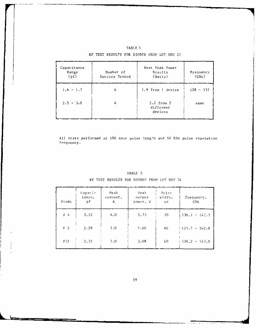
TABLE 4
RF TEST RESULTS FOR DIODES FROM LOT DDD 21
Capacitance Best Peak PowerRange Number of Results Frequency
(pf) Devices Tested (Watts) (Gliz)
1.6 - 1.7 4 1.9 from 1 device 128 - 131
2.5 - 3.0 4 2.2 from 2 samedifferent
devices
All tests performed at 100 nsec pulse length and 50 KHz pulse reputation
frequency.
TABLE 5
RF TEST RESULTS FOR DIODES FROM LOT DDV 54
Capaci- Peak Peak Pilz setance, current, outpu t width, Frequency,
Diode pf A power, W ns GHz
# 4 2.12 6.0 2.73 70 136.1 - 142.7
4 5 2.29 7.0 2.60 60 135.7 - 142.8
#12 2.15 7.0 3.08 60 136.2 - 143.0
59

W
2.0 watts of peak power over pulse lengths of up to 100 nsec. Table 4
shows test data from 8 diodes from lot DDD21 and also indicates the
effects of varying diode area. Table 5 illustrates the performance
from the diodes from lot DDD-54. In this case, note the almost identi-
cal rf performance from the 3 diodes tested.
Note that the best performing lots had doping densities (ND N A
17 -33-4 x 10 cm ) and breakdown voltages (Vb = 9-10 V) in good agreement
with the design values of Section 2.1.
All diodes were individually tested for output power and frequency res-
ponse in a standard single diode waveguide cavity circuit. This circuit
is shown schematically in Figure 25.
The test circuit consists of a 0.010 reduced height waveguide cavi.ty
with a tapered waveguide height transition to the WR-7 waveguide output.
Tuning was achieved by a sliding back short. A relatively large bias
pin with diameter between 0.027" and 0.035" was used in the cavity.
A bias pin of this size inside a 0.100" wide reduced height waveguide
can no longer be regarded as a thin inductive post, but rather a close
approximation to a step transformer whose lower face provides additional
impedance transformation between the IMPATT diode and the reduced height
waveguide load.
For the single diode characterization, all rf measurements were made
using a pulse repetition frequency of 50 K~lz. The width of the input
current pulse was adjustable between 80 ns and 130 ns. Many diodes
with different junction capacitances were tested, and the optimum capa-
citance which yielded the highest output power and the best rf tuning
characteristics was found to be between 2.0 pf and 2.5 pf. Figure 26
shows a typical input current pulse (top trace) and the corresponding
rf video pulse (bottom trace) for one of the high power diodes. The
peak power was 3.0W and the ;f pulse width was 100 ns. The frequency
60

GWO7
SIAS PIN
WR -7WA VEGU IDE
SLIDING PACKAGEDSHO0RT IMPATT
DIODE
Figure 25 Bias-pin transformer waveguidecircuit corP iguration.

t 2314
S20 i
px 11 n1put .'afrrolnt j'ii >c ( toll
ice i Uc 'upuL us
t~~~~o tu, thae I i .ii ue

chirp caused by transient thermal heating of the diode was from 139.0
CHz to 142.0 CHz. The conversion efficiency was 2.8%. Figure 27 sum-
marizes the performance of a high power 140 GHz diode from lot DDD54.
Shown are output power, frequency and efficiency as a function of pulse
bias current.
Based on these results, nearly all of the combiner development work
carried out during the latter months of the program, and including the
deliverable hardware, made use of diodes from Lot DDD 54. All of these
diodes were packaged in the double standoff configuration described
in Section 2.3.
4.3 TWO DIODE COMBINER CHARACTERIZATION
As discussed in Section 3.1, the basis for the final two diode combiner
was the enlarged Kurakawa circuit with the diodes mounted near the side-
walls. This configuration is shown in Figure 19.
Prior to testing in the combiner, the diodes were individually tested
for output power and frequency response in the standard single diode
circuit (Figure 25). Following is data for the diodes (Lot DDD 54)
which were delivered with the combiner circuit. Diode C-3 produced 1.0
watt of peak power with a frequency chirp due to transient thermal heat-
ing of 143 to 144.5 GC1z. Diode B-8 generated 2.5 watts of peak power
with a frequency chirp from 145.0 to 146.0 CGlz. They were then mounted
inside the resonator cavity and each was driven by a separate pulse
modulator. When both diodes were turned on at the same time and tuned
for maximum output power, a combined output of 3.0 watts peak power
was obtained. This implies that the combining efficiency was approxi-
mately to 90%. Figure 28(a) and 28(b) show the video rf output pulses
(bottom traces) for diodes DDD54C-3 and DDD54B-8, respectively, together
with their corresponding input current pulses (top traces). Figure 28 (c)
:shlws the combined rf output (bottom trace) when both diodes were turned
63

G66273.56
4
z.3.0 3 2L
U.Z
EFFICIENCY
22.6
OUTPUT POWER
m 2.0 141.0
I--
A1.
0 1.5 140.5
-
FREQUEN CY 2D r4w
1.0 140.00n"LLC
U.I.-z'U
0.5 139.5 C
I 139.02.0 3.0 4.0 5.0 6.0 7.0 8.0
BIAS CURRENT (AMPERES)
Figure 27 Operating characteristics of a high power
pulsed diode from lot DDD54.
64
LA

E2315
Figure 28(a) Video outp uts~ of input cu rret pulse(top) and rf output pulse (bottom)for diode DPD54C-3.
E2316
(, Xlp i c lre t ' i O

E231 7
I i 8c kie tOULI)L Of ilPUt current
pulse (top to traces) an dotu ule (bottom whon btde .',(: 3 ind )D -
,,, ore r

on. The current pulses (top two traces) for both diodes are also dis-
played for comparison. The frequency response of the combined r pulse
extended from 144.5 to 145.5 GHz and was clean and sharp throughout
90% of the pulse width, indicating true power combining.
A second circuit identical to the first one was constructed and two
more diodes were tested. In this case the center frequency was reduced
to 141.0 HHz, but the combined power was only 2.7 watts.
67

V PERFORMANCE OF DELIVERED UNITS
At the conclusion of the technical effort, and upon mutual agreement
with the Army, the following items were delivered:
1. One single-diode 3.0 watt IMPATT diode oscillator operating
at 140 GHz (Figure 29).
2. One single-diode pulse .odulator* with bias box and bias cable
(Figures 30 and 31).
3. One two-diode 3.0 watt IMPATT oscillator (Figure 32).
4. One two-diode pulse modulator* with bias boxes and bias cables
(Figures 33 and 34).
5. One D-Band isolator TRG model D112.
The detailed performance data for the single diode oscillator is summa-
rized in Figures 26 and 27.
The specifications for the single diode oscillator are given below:
Peak power out of intermediate waveguide 2.9 W
Peak power out of isolator 2.2 W
Center frequency 140.0 GHz
Frequency chirp 139.1-141.0 GHz
Pulse width 85 ns
Flatness within pulse I dB
*The modulators are very similar to standard Hughes commercial units.
Modulator development was not a part of this program.
68
[U

E2318
Vuic wat P;t:z c 9 IIos 1 llLor wit is lit)r

E2319
Figure 30 Single-diode pulse modulator.

£2320
Figure '31 Single diodie oscillator and.
Il 'so mnodl ator.

E2165
Figure 32 145 (Hz Twh - .iode combiner.

E2321
Figure 33 Two-diode pulse modulator.

L2082

The operating characteristics of the two diode oscillator/combiner are
described in Section 4.3. The specifications for this unit are as follows:
Peak output power 2.8W
Center frequency 145.5 CHz
Frequency chirp 145.0 - 146.0 GHz
Pulse width 80 ns
Complete operating instructions for the single and two-diode oscillators
are provided in Appendix A.
75

VI. CONCLUSIONS AND SUGGESTIONS FOR FUTURE WORK
Significant advances in the state-of-the-art for pulsed millimeter
wave diodes and oscillators operating near 140 GHz have been achieved
as a result of the work described in this report. Specific accomplish-
ments include:
1. The design and fabrication of silicon double drift IMPATT
diodes capable of peak output powers of over 3 watts at 140
GHz. The best single device result prior to this program
was about 800 mW of peak power.
2. The first time demonstration of efficient power combining
from two pulsed IMPATT diodes at 140 Chz.
3. The establishment of a basic resonant waveguide circuit config-
uration suitable for power combining from millimeter wave
IMPATT diodes.
4. The employment of a *onhermetic, but rugged double quartz
standoff package with appropriate parasitics for matching
power from high power pulsed diodes to variety of waveguide
circuits.
5. The delivery to the Army of two high power pulsed IMPATT oscil-
lators. Both of these oscillators meet the program objective
of 3.0 watts of output power, one from a single diode, the
other from a two-diode power combiner.
It seems probable that additional work on the diode, package and oscil-
lator circuit will lead to relatively modest improvements in single
diode oscillator performance. With this program, the groundwork has
been laid for further power combiner development work at 140 GHz. The
76

oversize Kurokowa circuit should provide the basis for combining power
from additional pairs of side-wall mounted diodes, for example 4 or
6 diodes. More recent experience with this circuit at lower frequencies
specifically at 60 and 94 GHz suggest that further progress with this
circuit is probably limited these numbers of diodes. The requirement
for additional power would then require higher level circuit combining
of two or more Kurakowa modules perhaps with hybrid couplers.
This situation suggests that fundamentally new approaches to millimeter
wave diode power combining are required, particularly at frequencies
above 100 GHz. A very promising approach is to employ quasi optical tech-
niques in conjunction with an open resonator combiner. This approach
is currently being pursued at Hughes under U.S. Army Electronics Research
and Development Command sponsorship. Another possibility which has
not yet received any significant attention at 140 Cllz is chip level
combining. Work at lower frequencies (60 and 94 GHz) with series and
parallel connections of diode chips however suggest this will be a
difficult technology to implement at 140 GHz.
77

REFERENCES
1. C. Canali et. al., "Electron and Hole Drift Velocity Measurements
in Silicon and Their Empirical Relation to Electric Field and Tem-
perature, " IEEE Trans. Electron Devices, Vol. ED-22, p. 1045,
November, 1975.
2. W. N. Grant, "El-ctron and Hole Ionization Rates in Epitaxial Sil-
icon at High Electric Fields, " Solid St. Electron., Vol. 16, p.
1189, 1973.
3. T. Misawa, " Negative Resistance in p-n Junction Under Avalanche
Breakdown Conditions, " Parts I and II, IEEE Trans. Electron Devices,
Vol. ED-13, pp. 137-151, January 1966.
4. T. Misawa, " Multiple Uniform Layer Approximation ia Analysis of
Negative Resistance in p-n Junction in Breakdown, " IEEE Trans.
Electron Devices, Vol. ED-14, pp. 795-808, December 1967.
5. J. C. Jaeger, " Pulsed Surface Heating of Semi-Infinite Solids,
" Australian Journal of Quarterly Mathematics, Vol. XI, pp. 123-
137, 1953.
6. K. Weller, Y. Ma, C. Chao, and E. M. Nakaji, "High Power V-Band
Amplifier, Final Report AFAL-TR-78-106-F, Contract No. F33615-
77-C-1061, Oct. 1978.
7. K. Kurokawa, "Single-Cavity Multiple-Device Oscillator, " lEE Trans
on Microwave Theory and Techniques, Vol. MT19, pp. 793 - 801, Oct.
1971.
8. R. S. Harp and H. L. Stover, " Power Combining of X-band IMPATT
Circuit Modules, " Digest of Technical Papers, 1973, IEEE Interna-
tional Solid State Circuits Conference, pp. 118-119.
78
r ,,,,., ,,., . , " = ' ,. '

APPENDIX A
OPERATION INSTRUCTIONS FOR THE 140 GHz SINGLE-DIODE
IMPATT OSCILLATOR AND TWO-DIODE IMPATT COMBINER
79

WARNING
BEFORE ATTEMPTING TO OPERATE ANY ITEMS,
PLEASE READ THE ATTACHED INSTRUCTIONS
VERY CAREFULLY. FAILURE TO DO SO MAY
RESULT IN UNNECESSARY OR IRREPARABLE
DAMAGE TO THE IMPATT OSCILLATORS AND
PULSE MODULATORS.
80

LIST OF DELIVERED ITEMS
One single-diode IMPATT oscillator (Figure 29).
One single-diode pulse modulator with bias box and bias cable
(Figures 30 aand 31).
One two-diode IMPATT oscillator (Figure 32).
One two-diode pulse modulator with bias boxes and bias cables, Hughes
model (Figures 33 and 34).
One D-Band isolator, TRG model D112.
81

OPERATION INSTRUCTIONS FOR THE SINGLE-DIODE IMPATT OSCILLATOR
1. GENERAL DESCRIPTION
The single-diode IMPATT oscillator (Figure 29) consists of three sec-
tions: the oscillator cavity, the intermediate waveguide, and the
isolator. Because of certain critical tuning elements, the oscillator
cavity and the intermediate waveguide should always remain together
as one unit. Under no circumstances should the two be separated.
The oscillator can be used with or without the isolator. Using the
isolator will ensure that the proper r.f. output is obtained. If the
isolator were not used, there is always the risk of having the oscil-
lator being detuned by the external load.
The single-diode pulse modulator (Figure 30) has been tuned to give
the IMPATT the best r.f. performance. No additional tuning is neces-
sary. Figure A-1 shows a typical test setup for the single diode
oscillator.
2. TO OPERATE THE IMPATT OSCILLATOR
1. Put the pulse modulator switch to OFF position.
2. Using a pulse generator with a 50 KHz PRF, a pulse width of
approximately 0.2 us, and a pulse height of approximately 2V,
supply a continuous train of square pulses into TRIG IN.
3. Supply +60V and +28V as indicated making sure the GROUND is
properly connected to all power supplies. The +28V terminal
should draw about 70 mA.
82

E2322
Fig -ire A-] Single diode os 1 ~lit- ttts~

4. Connect the OUTPUT terminal to the IMPATT oscillator using
the blue bias box marked with a letter "S" and any one of
the three white bias cables. See Figure 31 for detail. Do
not use the bias boxes marked "A" or "B".
5. To turn IMPATT on, simply put the pulse modulator switch to ON
position. The +60V terminal should be drawing about 80 mA.
Fig-ure 26 shows the current pulse and r.f. video output.
6. To turn IMPATT off, simply turn the pulse modulator switch
to the OFF position.
CAUTION:
BEFORE DISCONNECTING IMPATT FROM THE PULSE MODULATOR,
ALWAYS
a. Have pulse modulator switch in OFF position.
b. Turn off all power supplies.
c. Turn off pul'e generator.
Specifications:
Peak power out of intermediate
waveguide 2.9 W
Peak power out of isolator 2.2 W
Center frequency 140.0 GHz
Frequency chirp 139.1-141.0 GHz
Pulse width of chirp 85 ns
Flatness within chirp < 1 dB
84

OPERATION INSTRUCTIONS FOR THE TWO-DIODE IMPATT OSCILLATOR
1. GENERAL DESCRIPTION
The two-diode IMPATT oscillator (Figure 32) consists of the oscillator
cavity and the output waveguide. The two should always remain as one
unit. Furthermore, do not subject the oscillator to shock or vibration.
The oscillator is tuned to a center frequency of 145.5 GHz; as such
it may not be usable in a 140 GHz system. However, since it is a power
combiner, it may be used as a demonstration unit. To do so would only
require a D-Band detector, frequency meter and attenuator.
The two-diode pulse modulator (Figure 33) has been tuned for maximum
IMPATT performance. No further adjustments are necessary. Figure A-2
shows the two diode oscillator in a typical test setup.
2. TO OPERATE THE TWO-DIODE IMPATT OSCILLATOR
1. Put both pulse modulator switches to OFF position.
2. Using a pulse generator with a 50 KHz PRF, a pulse width of
approximately 0.2 vs, and a pulse width of approximately 21T,
supply a continuous train of square pulses into TRIG IN.
3. Supply +70V and +28V as indicated, making sure that the GROUND
terminal is properly connected to all power supplies.
4. Using the blue bias box marked "A" and a white bias cable,
connect out'ut terminal A OUT to the IMPATT input terminal
"A". Likewise, using the blue bias box marked "B" and another
white bias cable, connect output terminal B OUT to the IMPATT
input terminal "B". See Figure 34 for details.
85

E2 23
m. r
.
~
* 2

5. To turn on diode A (B), simply put pulse modulator switch A
(B) to ON position. To turn on both diodes, simply put both
switches to ON position. Use detector to observe the r.f.
video output. Figures 28 a, b and c show the current pulses
and r.f. video outputs for diode A, B and A + B, respectively.
NOTE: If diode A is turned on alone, its optimum r.f. video
output may not be observable because it occurs at a slightly
different tuning short position.
6. To turn off diode(s), put the appropriate switches to the
OFF position.
CAUTION:
BEFIRE CONNECTING IMPATT FROM THE PULSE
MODULATOR, ALWAYS
a. Have pulse modulator swithces in OFF position.
b. Turn off all power supplies.
c. Turn off pulse generator.
Specifications:
Peak output pow( 2.8W
Center frequency 145.5 GHz
Frequency chirp 145.0 - 146.0 GHz
Pulse width 80 ns
87

ADU 450 HUGHES AIRCRAFT CO TORRANCE CALIF TORRANCE RESEARCHl -E4" /S /140 GNZ PULSED IMPATT COMBINER HIGHi POWER SOUCE. (U)JAN 80 T T FONG. T A MIDPORD. E M NAKAJI DAAKII-7ThC-OAOo
UNCLASSIFIED HAC-N-425B5 ARBRL-CR-00414 NL
2-20 0000 [ND

DISTRIBUTION LIST
No. of No. ofCopies Organization Copies Organization
12 Commander 1 CommanderDefense Technical Info Center US Army Ballistic Missile DefenseATTN: DDC-DDA Advanced Technology CenterCameron Station ATTN: BMD-ATC-D, C. JohnsonAlexandria, VA 22314 P.O.Box 1500
Huntsville, AL 358072 Director of Defense Research
and Engineering 1 CommanderEngineering Technology TCATAATTN: L. Weisberg ATTN: Scientific Advisor
D. Charvonia Fort Hood, TX 76544Washington, DC 20301
1 Director2 Director US Army Research 4 Development
Defense Advanced Research Group (Europe)Projects Agency ATTN: Elct Br
ATTN: TTO, J. Tegnelia Box 15STO, S. Zakanycz FPO New York, NY 09510
1400 Wilson BoulevardArlington, VA 22209 1 Commander
US Army Materiel Development 4Director Readiness CommandDefense Nuclear Agency ATTN: DRCDMD-STATTN: STRA (RAEL) 5001 Eisenhower AvenueWashington, DC 20305 Alexandria, VA 22333
Director 1 CommanderInstitute for Defense Analysis US Army Materiel Development &ATTN: V. Corcoran Readiness Command400 Army-Navy Drive ATTN: DRCBSI, P. DickinsonArlington, VA 20305 5001 Eisenhower Avenue
Alexandria, VA 223331 HQDA (DAMA-DDZ-C)
Washington, DC 20310 8 CommanderUS Army Armament Research and
1 HQDA (DAMA-CSM-CA/LTC N. Conner) Development CommandWashington, DC 20310 ATTN: DRDAR-TSS (2 cys)
DRDAR-SC, J. Lehman1 HQDA (SARD) J. Heberly
Assistant for Electronics DRuAR-LCU-DE, T. Malgeri
ATTN: V. Friedrich DRDAR-LCS, P. KruegerWashington, DC 20310 DRCPM-SA, J. Brooks
Dover, NJ 07801
89

DISTRIBUTION LIST
No. of No. ofCopies Organization Copies Organization
Commander 4 CommanderUS Army Armament Materiel I'S Army Electronics Research
Readiness Command & Development CommandATTN: DRSAR-LEP-L, Tech Lib ATTN: DELSD-LRock Island, IL 61299 DRDEL-CT
DRDEL-RDDirector DRDEL-VT, Mr. PostUS Army ARRADCOM Fort Monmouth, NJ 07703Benet Weapons LaboratoryATTN: DRDAR-LCB-TL 4 CommanderWatervliet, NY 12189 US Army Electronics Research &
Development CommandCommander ATTN: DELET-MJ, H. JacobsUS Army Aviation Research & DELCS-R-CSTA, R. Pearce
Development Command DELNV-L, R.BuserATTN: DRSAV-E R. RohdeP.O. Box 209 Fort Monmouth, NJ 07703St. Louis, MO 63166
1 Office of Test DirectorDirector Joint Services LGW/CM TestUS Army Air Mobility Research Program
and Development Laboratory ATTN: DRDEL-WL-MT, R. MurrayAmes Research Center White Sands Missile Range, NMMoffett Field, CA 94035 88002
Commander 1 CommanderUS Army Communication Research US Army Electronics Research &
and Development Command Development CommandATTN: DRDCO-PPA-SA ATTN: DRDEL-BL-RD, Atmos SciFort Monmouth, NJ 07703 Rsch
Fort Huachuca, AZ 856132 Commander
US Army Electronics Research 8 CommanderDevelopment Command US Army Harry Diamond
ATTN: DRDEL-AP-CCM, D.Giglio LaboratoriesDRDEL-AP-FI, D. Gormley ATTN: DELHD-NMM, E. Brown
2800 Powder Mill Road S. KulpaAdelphi, MD 20783 B. Weber
DELHD-RA, J. SalernoDELHD- RAC, R. Humphrey
DELHD-RCB, G. SimonisDELHD-DBE, T. GleasonDELHD-TD
2800 Powder Mill RoadAdelphi, MD 20783
90

DISTRIBUTION LIST
No. of No. of
Copies Organization Copies Organization
2 Director I Commander
US Army Atmospheric Sciences US Army Mobility Equipment
Laboratory Research & Development Cmd
ATTN: DRSEL-BL-AS-P, K.White ATTN: SMEFB-EM, K.Steinback
Don Snider Fort Belvoir, VA 22060
White Sands Missile Range,NM 88002 1 Commander
US Army Tank Automotive Research
2 Director & Development Command
US Army Night Vision Laboratory ATTN: DRDTA-UL
ATTN: DRSEL-NV-VI, J.Moulton Warren, MI 48090
DRSEL-NV-lI, R.ShurtzFort Belvoir, VA 22060 1 Commander
US Army White Sands Missile
Director RangeOffice of Missile Electronic ATTN: STEWS-TE, J.Flores
Warfare White Sands Missile Range,
ATTN: DRSEL-WLH-SF,R.Clawson NM 88002
White Sands Missile RangeNM 88002 1 Commander
US Army Foreign Science &
7 Commander Technology Center
US Army Missile Command ATTN: DRXST-SD, 0. HarrisATTN: DRDMI-TR, R.Hartman 220 7th Street NE
DRDMI-TRO, B. Guenther Charlottesville, VA 22901W.Gamble
DRDMI-REO, G.Emmons 3 Commander
DRDMI-R,Mr. Pittman US Army Research Office
DRDAR-RBL ATTN: D. Van Hulsteyn
DRDAR-RES R. Lontz
Redstone Arsenal, AL 35809 T. MinkP.O. Box 12211
7 Commander Research Triangle Park, NC
US Army Missile Command 27709
ATTN: DRDMI-RER, Ht. GreenDRDMI-R 1 Commander
DRDMI-YDL US Army TRADOC Systems Analysis
DRDMI-RF, C. Hussey Activity
DRDMI-RFC,A. Michetti ATTN: ATAA-SL, Tech Lib
DRDMI-RFE, Mr.Duvall White Sands Missile Range,
DRDMI-YDC,Mr.Salonimer NM 88002
Redstone Arsenal, AL 358091 Commander
Naval Air Systems CommandATTN: AIR-2324, C. Francis
Washington, DC 20360
91

DISTRIBUTION LIST
No. of No. ofCopies Organization Copies Organization
Commander 1 ADTC/DLOFL, Tech LibCenter for Naval Analyses Eglin AFB, FL 32542ATIN: Docu Control1401 Wilson Boulevard I ADTC/DLMTArlington, VA 22209 Eglin AFB, FL 32542
Commander 1 ADTC/ADANaval Air Development Center Eglin AFB, FL 32542ATTN: AETD, Radar DivWarminster, PA 18974 1 AFATL/DLB
Eglin AFB, FL 325422 Commander
Naval Electronics Lab Center I AFATL/DLTG, C. BrownATTN: Code 2330, J. Provencher Eglin AFB, FL 32S42
Tech LibSan Diego, CA 92152 2 AFATL/DLYW/DLDG
Eglin AFB, FL 325422 Commander
Naval Surface Weapons Center 1 RADC/EMATEATTN: Lib Griffiss AFB, NY 13440
Code DF34Dahlgren, VA 22448 1 RADC/ETEN
Griffiss AFB, NY 134403 Commander
Naval Weapons Center 3 AFGL/LZ, C. Sletten; LZN, E.ATTN: Code 6014, J. Battles Altschuler; S. Clough
R. Moore Hanscom AFB, MA 01730R. Higuera
China Lake, CA 93555 I AFWL/SULKirtland AFB, NM 87117
3 CommanderNaval Research Laboratory 1 AFAL/WRW, Mr. LeasureATTN: Code 5300, Radar Div. Wright-Patterson AFB, OH 45433
Dr. SkolnikCode 5370, Radar 1 AFAL/RWN-1, R. Bruns
Geophysics Br. Wright-Patterson AFB, OH 45433Code 5460, EM Prop Br.
Washington, DC 20375 1 DirectorNational Bureau of Standards
3 Commander ATTN: Div 276, 106, C.MillerNaval Research Laboratory Boulder, CO 80302ATTN: Code 7110, B. Yaplee
Code 7122.1,K. Shivanandan
Code 7111, J. Hollinger
Washington, DC 2037592

DISTRIBUTION LIST
No. of No. ofCopies Organization Copies Organization
Director 1 Hughes Aircraft CompanyNational Oceanographic & Aerospace Group
Atmospheric Administration Radar DivisionATIN: V. Derr ATTN: R. WagnerBoulder, CO 80303 Culver City, CA 90230
3 The Ivan A. Getting Laboratory 4 Hughes Aircraft CompanyThe Aerospace Corporation Aerospace GroupATTN: T. Hartwick, E. Epstein Electron Dynamic Division
D. Hodges ATTN: N. Kramer
P.O. Box 92957 J. SparacioLos Angeles, CA 90009 R. Ying
M. Kaswen
Ford-Aeronutronic 3100 West Lomita Boulevard
ATTN: D. Burch Torrance, CA 90504Ford RoadNewport, CA 92663 1 Martin Marietta Corporation
ATTN: F. Wilcox
General Electric-TEMPO P.O.Box 5837
ATTN: V.R. Stull Orlando, FL 32805816 State Street
Santa Barbara, CA 93102 1 The Rand CorporationATTN: S. Dudzinsky
2 Honeywell Corporate Research 1700 Main Street
Center Santa Monica, CA 90406ATTN: P. Kruse
C. Seashore 1 The R&D Associates10701 Lyndale Avenue South ATTN: G. GordonBloomington, MN 55420 P.O. Box 9695
Marina Del Rey, CA 90291
Honeywell, Inc.ATTN: A.C. Hastings 1 Raytheon Company
600 Second Street North Missiles Systems Division
Hopkins, MN 55343 ATTN: W. JusticeHartwell Road
Hughes Aircraft Company Bedford, MA 01730
Aerospace GroupAdvanced Program Development 1 Sperry Rand Corporation
Systems Division Microwave Electronics Division
ATTN: M. Bebe ATTN: R. RoderCanoga Park, CA 91304 Clearwater, FL, 33518
93

DISTRIBUTION LIST
No. of No. ofCopies Organization Copies Organization
2 System Planning Corporation 1 Lincoln Laboratory, MITATTN: J. Meni ATTN: C. Blake
R. Harris P.O. Box 731500 Wilson Boulevard Lexington, MA 02173Arlington, VA 22209
2 University of IllinoisUnited Aircraft Corporation Department of ElectricalNorden Division Engineering EERL-200ATTN: Dr. L. Kosowsky ATTN: T. DeTempleHelen Street P. ColemanNorwalk, CT 06852 Urbana, IL 61801
5 Georgia Institute of Technology Aberdeen Proving GroundEngineering Experiment StationATTN: J. Wiltse Dir, USAMSAA
R. Hayes ATTN: DRXSY-DF. Dyer DRXSY-MP, H. CohenJ. Dees Cdr, USATECOMJ. Gallagher ATTN: DRSTE-TO-F
347 Ferst Drive J. PhillipsAtlanta, GA 30332 Bldg 314
2 Director Dir, Wpns Sys Concepts TeamApplied Physics Laboratory Bldg E3516, EAThe Johns Hopkins University ATTN: DRDAR-ACWATTN: A. Stone
LibJohns Hopkins RoadLaurel, MD 20810
Francis Bitter National MagnetLab, MIT
ATTN: K. Button170 Albany StreetCambridge, MA 02139
94

USER EVALUATION OF REPORT
Please take a few minutes to answer the questions below; tear outthis sheet and return it to Director, US Army Ballistic ResearchLaboratory, ARRADCOM, ATTN: DRDAR-TSB, Aberdeen Proving Ground,Maryland 21005. Your comments will provide us with informationfor improving future reports.
1. BRL Report Number
2. Does this report satisfy a need? (Comment on purpose, relatedproject, or other area of interest for which report will be used.)
3. How, specifically, is the report being used? (Informationsource, design data or procedure, management procedure, source ofideas, etc.)
4. Has the information in this report led to any quantitativesavings as far as man-hours/contract dollars saved, operating costsavoided, efficiencies achieved, etc.? If so, please elaborate.
5. General Comments (Indicate what you think should be changed tomake this report and future reports of this type more responsiveto your needs, more usable, improve readability, etc.)
6. If you would like to be contacted by the personnel who preparedthis report to raise specific questions or discuss the topic,please fill in the following information.
Name:
Telephone Number:
Organization Address:

7'I' A T E
ILMEI