
EIE/ENE 334 Microprocessors -...
68
EIE/ENE 334 Microprocessors Lecture 8: ARM Cortex-M0 Processors http://webstaff.kmutt.ac.th/~dejwoot.kha/ Week #08 : Dejwoot KHAWPARISUTH Adapted from
Transcript of EIE/ENE 334 Microprocessors -...

EIE/ENE 334
Microprocessors
Lecture 8:
ARM Cortex-M0 Processors
http://webstaff.kmutt.ac.th/~dejwoot.kha/
Week #08 : Dejwoot KHAWPARISUTH
Adapted from

Textbooks:
Joseph Yiu, “The Definitive Guide to the ARM Cortex-M0”, Newnes, 2011
http://www.arm.com/support/university/academic-resources.php
Page 2EIE/ENE 334 ARM Cortex-M0

Ref: from ARM
For Final exam: Cortex™-M0 Devices Generic User Guide (DUI0497A)
Page 3EIE/ENE 334 ARM Cortex-M0

Ref: from Nuvoton
Page 4EIE/ENE 334 ARM Cortex-M0
For Final exam: NuMicro NUC130_140 Technical Reference Manual EN V2.02

ARM-Cortex-M0 Intro
Page 5
➔ 32-bit RISC processor
➔ a 3-stage pipeline von
Neumann architecture
➔ the ARMv6-M architecture
➔ Implement
➔ the ARMv6-M Thumb®
instruction set
➔ including Thumb-2
technology
Week #08 EIE/ENE 334 ARM Cortex-M0

ARM-Cortex-M0 Intro
Page 6
➔ 56 instructions (16&32 bits)
➔ Microcontroller applications
➔ Zero jitter (the instruction
and interrupt timings are
fully deterministic)
➔ Include a nested vector
interrupt controller (NVIC)
➔ Support the CoreSight Debug
architecture
Week #08 EIE/ENE 334 ARM Cortex-M0

ARM-Cortex-M0 Intro
Page 7
➔ very low gate count
(12,000 logic gates,
minimum configuration)
➔ highly energy efficient
(0.9 DMIPS/MHz)
➔ Code density using Thumb-
2-based instruction
Week #08 EIE/ENE 334 ARM Cortex-M0
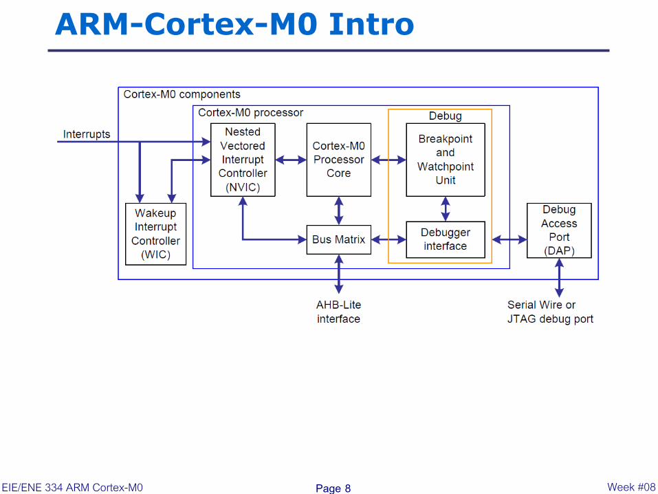
ARM-Cortex-M0 Intro
Page 8 Week #08 EIE/ENE 334 ARM Cortex-M0

ARM-Cortex-M0 Core
Page 9
➔ Programmer’s model
➔ Instruction set
➔ Exception mechanism
➔ Memory model
➔ Debug architecture
Week #08 EIE/ENE 334 ARM Cortex-M0

Programmer’s model
Page 10
➔ Two states
➔ Thumb state
➔ Two operation modes
➔ Thread mode (can use
a shadowed stack
pointer)
➔ Handler mode
➔ Debug state
Week #08 EIE/ENE 334 ARM Cortex-M0

Programmer’s model
Page 11
➔ Core registers
Week #08 EIE/ENE 334 ARM Cortex-M0

Programmer’s model
Page 12
- A load-store architecture
- The processor uses a full
descending stack: PUSH –
decrements the stack pointer
and then writes the item onto
the stack.
Week #08 EIE/ENE 334 ARM Cortex-M0

Programmer’s model
Page 13
- On reset, the processor
loads the MSP with the value
from address 0x00000000.
- In Handler mode, the
processor always use the main
stack (MSP).
Week #08 EIE/ENE 334 ARM Cortex-M0

Programmer’s model
Page 14
- After reset, the main stack
pointer (MSP) is used, but can
be switched to the process stack
pointer (PSP) in Thread mode
(when not running an exception
handler) by setting bit [1] in
the CONTROL register. During
running of an exception handler,
the CONTROL register reads as
zero.
Week #08 EIE/ENE 334 ARM Cortex-M0

Programmer’s model
Page 15
- The CONTROL register can
only be changed in Thread
mode or via the exception
entrance and return
mechanism.
Week #08 EIE/ENE 334 ARM Cortex-M0
Programmer’s model
Page 16
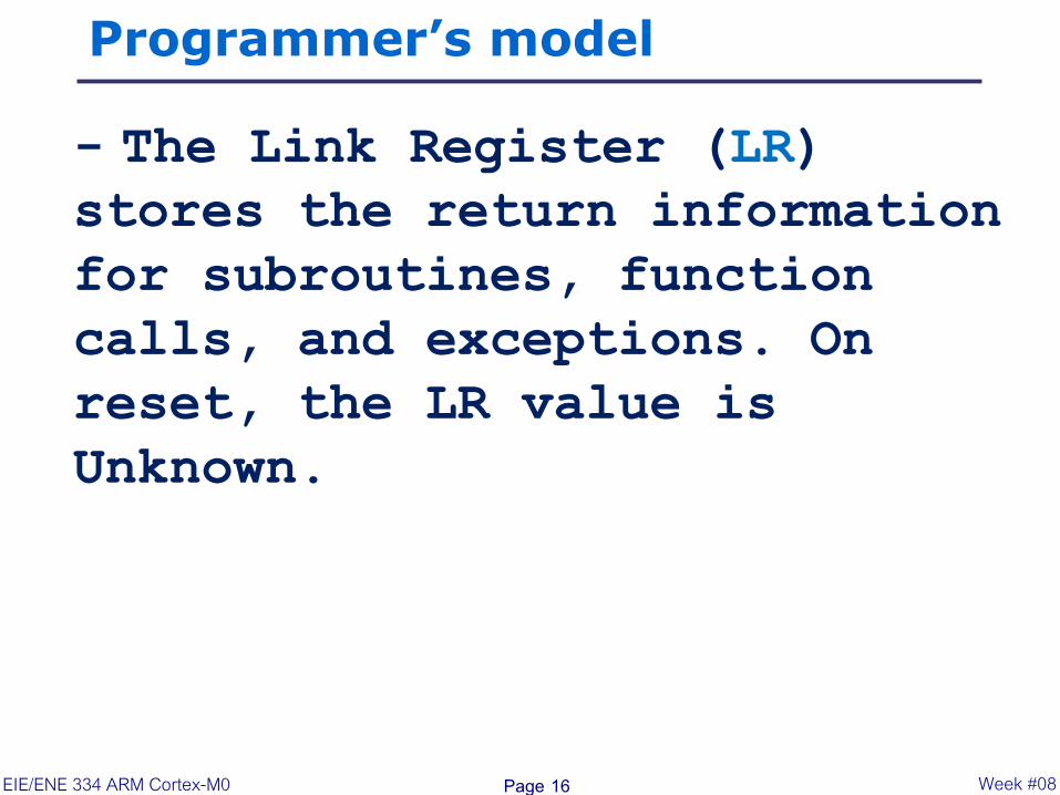
- The Link Register (LR)
stores the return information
for subroutines, function
calls, and exceptions. On
reset, the LR value is
Unknown.
Week #08 EIE/ENE 334 ARM Cortex-M0

Programmer’s model
Page 17
- The Program Counter (PC)
contains the current program
address. On reset, the
processor loads the PC with
the value of the reset vector,
at address 0x00000004. Bit[0]
of the value is loaded into
the EPSR T-bit at reset and
must be 1.
Week #08 EIE/ENE 334 ARM Cortex-M0

Programmer’s model
Page 18
- The Program Status Register
(PSR) combines:
Week #08 EIE/ENE 334 ARM Cortex-M0
Programmer’s model
Page 19
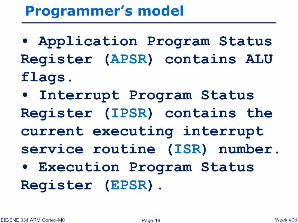
• Application Program Status
Register (APSR) contains ALU
flags.
• Interrupt Program Status
Register (IPSR) contains the
current executing interrupt
service routine (ISR) number.
• Execution Program Status
Register (EPSR).
Week #08 EIE/ENE 334 ARM Cortex-M0
Programmer’s model
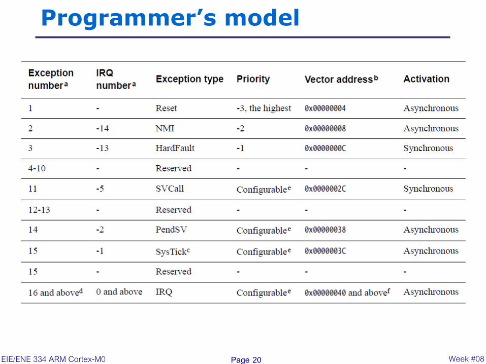
Page 20 Week #08 EIE/ENE 334 ARM Cortex-M0

Programmer’s model
Page 21 Week #08 EIE/ENE 334 ARM Cortex-M0
- The PRIMASK register
prevents activation of all
exceptions with configurable
priority.
0 = no effect (on RESET)
1 = prevents the activation of all exceptions with configurable priority.
22University Program Material
Copyright © ARM Ltd 2012
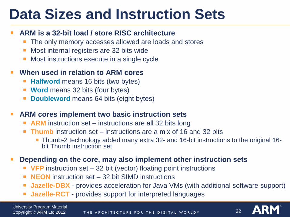
Data Sizes and Instruction Sets
ARM is a 32-bit load / store RISC architecture
The only memory accesses allowed are loads and stores
Most internal registers are 32 bits wide
Most instructions execute in a single cycle
When used in relation to ARM cores
Halfword means 16 bits (two bytes)
Word means 32 bits (four bytes)
Doubleword means 64 bits (eight bytes)
ARM cores implement two basic instruction sets
ARM instruction set – instructions are all 32 bits long
Thumb instruction set – instructions are a mix of 16 and 32 bits
Thumb-2 technology added many extra 32- and 16-bit instructions to the original 16-bit Thumb instruction set
Depending on the core, may also implement other instruction sets
VFP instruction set – 32 bit (vector) floating point instructions
NEON instruction set – 32 bit SIMD instructions
Jazelle-DBX - provides acceleration for Java VMs (with additional software support)
Jazelle-RCT - provides support for interpreted languages

23University Program Material
Copyright © ARM Ltd 2012
Which architecture is my processor?

24University Program Material
Copyright © ARM Ltd 2012
Embedded Processors

25University Program Material
Copyright © ARM Ltd 2012
Halfword and
signed halfword
/ byte support
System mode
Thumb
instruction set
(v4T)
Improved
interworking
CLZ
Saturated arithmetic
DSP MAC
instructions
Extensions:
Jazelle (5TEJ)
SIMD Instructions
Multi-processing
v6 Memory architecture
Unaligned data support
Extensions:
Thumb-2 (6T2)
TrustZone® (6Z)
Multicore (6K)
Thumb only (6-M)
Note that implementations of the same architecture can be different
Cortex-A8 - architecture v7-A, with a 13-stage pipeline
Cortex-A9 - architecture v7-A, with an 8-stage pipeline
Thumb-2
Architecture Profiles
7-A - Applications
7-R - Real-time
7-M - Microcontroller
v4 v5 v6 v7
Development of the ARM Architecture

26University Program Material
Copyright © ARM Ltd 2012
Instruction Set basics
The ARM Architecture is a Load/Store architecture
No direct manipulation of memory contents
Memory must be loaded into the CPU to be modified, then written back out
Cores are either in ARM state or Thumb state
This determines which instruction set is being executed
An instruction must be executed to switch between states
The architecture allows programmers and compilation tools to reduce
branching through the use of conditional execution
Method differs between ARM and Thumb, but the principle is that most (ARM) or
all (Thumb) instructions can be executed conditionally.

27University Program Material
Copyright © ARM Ltd 2012
Data Processing Instructions
These instructions operate on the contents of registers
They DO NOT affect memory
Syntax:
<Operation>{<cond>}{S} {Rd,} Rn, Operand2
Examples:
ADD r0, r1, r2 ; r0 = r1 + r2
TEQ r0, r1 ; if r0 = r1, Z flag will be set
MOV r0, r1 ; copy r1 to r0
arithmetic logical move
manipulation
(has destination
register)
ADD
ADC
SUB
SBC
RSB
RSC
AND EOR MOV
comparison
(set flags only)
CMN(ADDS)
CMP(SUBS)
TST(ANDS)
TEQ(EORS)
ORR
ORN
BIC MVN

28University Program Material
Copyright © ARM Ltd 2012
Single Access Data Transfer
Use to move data between one or two registers and memory
LDRD STRD Doubleword
LDR STR Word
LDRB STRB Byte
LDRH STRH Halfword
LDRSB Signed byte load
LDRSH Signed halfword load
Syntax:
LDR{<size>}{<cond>} Rd, <address>
STR{<size>}{<cond>} Rd, <address>
Example:
LDRB r0, [r1] ; load bottom byte of r0 from the
; byte of memory at address in r1
Upper bits zero filled or
sign extended on Load
Memory
Rd
31 0

29University Program Material
Copyright © ARM Ltd 2012
These instructions move data between multiple registers and memory
Syntax
<LDM|STM>{<addressing_mode>}{<cond>} Rb{!}, <register list>
4 addressing modes
Increment after/before
Decrement after/before
Also
PUSH/POP, equivalent to STMDB/LDMIA with SP! as base register
Example
LDM r10, {r0,r1,r4} ; load registers, using r10 base
PUSH {r4-r6,pc} ; store registers, using SP base
Multiple Register Data Transfer
(IA)
r1 Increasing
Address
r4
r0
r1
r4
r0
r1
r4
r0 r1
r4
r0
r10
IB DA DB
Base Register (Rb)

30University Program Material
Copyright © ARM Ltd 2012
:
BL func2
:
:
BX lr
func1 func2void func1 (void)
{
:
func2();
:
}
Subroutines
Implementing a conventional subroutine call requires two steps
Store the return address
Branch to the address of the required subroutine
These steps are carried out in one instruction, BL
The return address is stored in the link register (lr/r14)
Branch to an address (range dependent on instruction set and width)
Return is by branching to the address in lr

31University Program Material
Copyright © ARM Ltd 2012
Supervisor Call (SVC)
SVC{<cond>} <SVC number>
Causes an SVC exception
The SVC handler can examine the SVC number to decide what operation
has been requested
But the core ignores the SVC number
By using the SVC mechanism, an operating system can implement a set
of privileged operations (system calls) which applications running in user
mode can request
Thumb version is unconditional

32University Program Material
Copyright © ARM Ltd 2012
Cortex-M0
Cortex M3 Total
60k* Gates
ARMv6-M Architecture
16-bit Thumb-2 with system control
instructions
Fully programmable in C
3-stage pipeline
von Neuman architecture
AHB-Lite bus interface
Fixed memory map
1-32 interrupts
Configurable priority levels
Non-Maskable Interrupt support
Low power support
Core configured with or without
debug
Variable number of watchpoints and
breakpoints

33University Program Material
Copyright © ARM Ltd 2012
Binary Upwards Compatibility
ARMv6-M
Architecture
ARMv7-M
Architecture

Instruction set
Page 34 Week #08 EIE/ENE 334 ARM Cortex-M0
- only the 16-bit Thumb
instructions
- and a minimum subset of 32-
bit Thumb instructions
Assembly syntax (ARM assembler)
label mnemonic operand1, operand2,… ; Comment
label -> used as a reference to an address location (optional) and data
address (start at the first column in the line)

Assembly syntax (ARM assembler)
Page 35 Week #08 EIE/ENE 334 ARM Cortex-M0
Immediate data: prefixed with “#”
example:
label mnemonic operand1, operand2,… ; Comment
MOVS R0,#0x1F ; Set R0 = 0x1F
MOVS R0,#’A’ ; Set R0 = 0x41 (ASCII code)

Assembly syntax (ARM assembler)
Page 36 Week #08 EIE/ENE 334 ARM Cortex-M0
Constant definition:
example:
label mnemonic operand1, operand2,… ; Comment
CLK_BA_base EQU 0x50000200 ; 32-bits
PWRCON EQU 0x00 ; 8-bits?

Assembly syntax (ARM assembler)
Page 37 Week #08 EIE/ENE 334 ARM Cortex-M0
Embedded data:
example: (LDR is a pseudo instruction)
label mnemonic operand1, operand2,… ; Comment
LDR R0,=MyData ; Get the address of MyData
LDR R1,[R0] ; R1 = 0x12345678
LDR R0,=MyText ; R0 = the starting addr
LDR R1,[R0] ; R1 = 0x61434241
MyData DCD 0x12345678
MyText DCB "Hi ABCabc01234\n",0 ; Null terminated
; string

Assembly syntax (ARM assembler)
Page 38 Week #08 EIE/ENE 334 ARM Cortex-M0
26: LDR R0,=MyData ; Get the address of MyData
0x0000016E 4807 LDR r0,[pc,#28] ; @0x0000018C
27: LDR R1,[R0] ; R1 = 0x12345678
28:
0x00000170 6801 LDR r1,[r0,#0x00]
29: LDR R0,=MyText ; R0 = the starting addr
0x00000172 4807 LDR r0,[pc,#28] ; @0x00000190
30: LDR R1,[R0]
31:
32: ALIGN 4
33: MyData DCD 0x12345678
34: MyText DCB "ABCabc0123\n",0 ; Null terminated string
35: }
0x00000174 6801 LDR r1,[r0,#0x00]
0x00000176 0000 MOVS r0,r0
0x00000178 5678 LDRSB r0,[r7,r1]
0x0000017A 1234 ASRS r4,r6,#8
0x0000017C 4241 RSBS r1,r0,#0
0x0000017E 6143 STR r3,[r0,#0x14]
0x00000180 6362 STR r2,[r4,#0x34]
0x00000182 3130 ADDS r1,r1,#0x30
0x00000184 3332 ADDS r3,r3,#0x32
0x00000186 000A MOVS r2,r1

Instruction set: Memory access
Page 39 Week #08 EIE/ENE 334 ARM Cortex-M0
ADR: Generates a PC-relative address.
example:
20: ADR R0, MyData
; write address 0x0000016C to R0
; R0 = 0x0000016C
21:
22: ALIGN 4
23: MyData DCD 0x12345678
0x00000168 A000 ADR r0,{pc}+4
; @0x0000016C
0x0000016A 0000 MOVS r0,r0
0x0000016C 5678 LDRSB r0,[r7,r1]
0x0000016E 1234 ASRS r4,r6,#8

Instruction set: Memory access
Page 40 Week #08 EIE/ENE 334 ARM Cortex-M0
LDR and STR, immediate offset
example:
LDR R0, [R5]
; Loads R0 from the address in R5.
STR R1, [R6,#const-struc]
; const-struc is an expression evaluating
; to a constant in the range 0-1020.

Instruction set: Memory access
Page 41 Week #08 EIE/ENE 334 ARM Cortex-M0
LDR and STR, register offset
example:
STR R0, [R5, R1]
; Store value of R0 into an address equal to
; sum of R5 and R1
LDRSH R1, [R2, R3]
; Load a halfword from the memory address
; specified by (R2 + R3), sign extend to 32-bits
; and write to R1.
Instruction set: Memory access
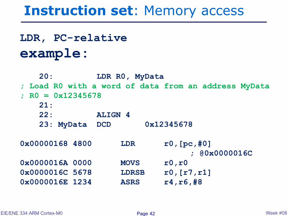
Page 42 Week #08 EIE/ENE 334 ARM Cortex-M0
LDR, PC-relative
example:
20: LDR R0, MyData
; Load R0 with a word of data from an address MyData
; R0 = 0x12345678
21:
22: ALIGN 4
23: MyData DCD 0x12345678
0x00000168 4800 LDR r0,[pc,#0]
; @0x0000016C
0x0000016A 0000 MOVS r0,r0
0x0000016C 5678 LDRSB r0,[r7,r1]
0x0000016E 1234 ASRS r4,r6,#8

Instruction set: Memory access
Page 43 Week #08 EIE/ENE 334 ARM Cortex-M0
LDM and STM: Load and Store Multiple
registers.
example:
LDM R0,{R0,R3,R4}
; LDMIA,LDMFD is a synonym for LDM
; R0=memory[R0], R3=memory[R0+4}, R4=memory[R0+8]
STMIA R1!,{R2-R4,R6}
; memory[R1]=R2, memory[R1+4]=R3, memory[R1+8]=R4,
; memory[R1+12]=R6, and update R1

Instruction set: Memory access
Page 44 Week #08 EIE/ENE 334 ARM Cortex-M0
PUSH and POP:
example:
PUSH {R0,R4-R7}
; Push R0,R4,R5,R6,R7 onto the stack
PUSH {R2,LR}
; Push R2 and the link-register onto the stack
POP {R0,R6,PC}
; Pop r0,r6 and PC from the stack, then branch to
; the new PC.

Instruction set: data processing
Page 45 Week #08 EIE/ENE 334 ARM Cortex-M0
ADC, ADD, RSB, SBC, and SUB: Add with
carry, Add, Reverse Subtract,
Subtract with carry, and Subtract.
example: shows two instructions that add a 64-
bit integer contained in R0 and R1 to
another 64-bit integer contained in R2 and R3, and
place the result in R0 and R1.
ADDS R0, R0, R2
; add the least significant words
ADCS R1, R1, R3
; add the most significant words with carry

Instruction set: data processing
Page 46 Week #08 EIE/ENE 334 ARM Cortex-M0
ADC, ADD, RSB, SBC, and SUB: Add with
carry, Add, Reverse Subtract,
Subtract with carry, and Subtract.
example: shows the RSBS instruction used to
perform a 1's complement of a single
register.
RSBS R7, R7, #0
; subtract R7 from zero
S-Suffic indicate an instruction that update
APSR(flags: N, Z, C, and V)

Instruction set: data processing
Page 47 Week #08 EIE/ENE 334 ARM Cortex-M0
AND, ORR, EOR, and BIC: Logical AND,
OR, Exclusive OR, and Bit Clear.
example:
ANDS R2, R2, R1
ORRS R2, R2, R5
ANDS R5, R5, R8
EORS R7, R7, R6
BICS R0, R0, R1

Instruction set: data processing
Page 48 Week #08 EIE/ENE 334 ARM Cortex-M0
ASR, LSL, LSR, and ROR: Arithmetic
Shift Right, Logical Shift Left,
Logical Shift Right, and Rotate
Right.
example:
ASRS R7, R5, #9
; Arithmetic shift right by 9 bits
LSLS R1, R2, #3
; Logical shift left by 3 bits with flag update
LSRS R4, R5, #6
; Logical shift right by 6 bits
RORS R4, R4, R6
; Rotate right by the value in
; the bottom byte of R6.

Instruction set: data processing
Page 49 Week #08 EIE/ENE 334 ARM Cortex-M0
CMP and CMN: Compare and Compare
Negative.
example:
CMP R2, R9
CMN R0, R2

Instruction set: data processing
Page 50 Week #08 EIE/ENE 334 ARM Cortex-M0
MOV and MVN: Move and Move NOT.
example:
MOVS R0, #0x000B
; Write value of 0x000B to R0, flags get updated
MOVS R1, #0x0
; Write value of zero to R1, flags are updated
MOV R10, R12
; Write value in R12 to R10, flags are not updated
MOVS R3, #23
; Write value of 23 to R3
MOV R8, SP
; Write value of stack pointer to R8
MVNS R2, R0
; Write inverse of R0 to the R2 and update flags

Instruction set: data processing
Page 51 Week #08 EIE/ENE 334 ARM Cortex-M0
MULS: Multiply using 32-bit operands,
and producing a 32-bit result.
example:
MULS R0, R2, R0
; Multiply with flag update, R0 = R0 x R2

Instruction set: data processing
Page 52 Week #08 EIE/ENE 334 ARM Cortex-M0
REV, REV16, and REVSH: Reverse bytes.
example:
REV R3, R7
; Reverse byte order of value in R7 and write it
; to R3
REV16 R0, R0
; Reverse byte order of each 16-bit halfword in R0
REVSH R0, R5
; Reverse signed halfword

Instruction set: data processing
Page 53 Week #08 EIE/ENE 334 ARM Cortex-M0
SXT and UXT: Sign extend and Zero
extend.
example:
SXTH R4, R6
; Obtain the lower halfword of the
; value in R6 and then sign extend to
; 32 bits and write the result to R4.
UXTB R3, R1
; Extract lowest byte of the value in R10 and zero
; extend it, and write the result to R3

Instruction set: data processing
Page 54 Week #08 EIE/ENE 334 ARM Cortex-M0
TST: Test bits.
example:
TST R0, R1
; Perform bitwise AND of R0 value and R1 value,
; condition code flags are updated but result is
; discarded

Instruction set: Branch and control
Page 55 Week #08 EIE/ENE 334 ARM Cortex-M0
B, BL, BX, and BLX: Branch
instructions.
example:
B loopA
; Branch to loopA
BL funC
; Branch with link (Call) to function funC, return
; address stored in LR
BX LR
; Return from function call
BLX R0
; Branch with link and exchange (Call) to a
; address stored in R0
BEQ labelD
; Conditionally branch to labelD if last flag
; setting instruction set the Z flag, else do not branch.

Condition code suffixes
Page 56 Week #08 EIE/ENE 334 ARM Cortex-M0

Instruction set: Miscellaneous
Page 57 Week #08 EIE/ENE 334 ARM Cortex-M0
BKPT: Breakpoint.
example:
BKPT #0
; Breakpoint with immediate value set to 0x0.

Instruction set: Miscellaneous
Page 58 Week #08 EIE/ENE 334 ARM Cortex-M0
CPS: Change Processor State.
example:
CPSID i
; Disable all interrupts except NMI (set PRIMASK)
CPSIE i
; Enable interrupts (clear PRIMASK)

Instruction set: Miscellaneous
Page 59 Week #08 EIE/ENE 334 ARM Cortex-M0
DMB: Data Memory Barrier.
example:
DMB
; Data Memory Barrier

Instruction set: Miscellaneous
Page 60 Week #08 EIE/ENE 334 ARM Cortex-M0
DSB: Data Synchronization Barrier.
example:
DSB
; Data Synchronization Barrier

Instruction set: Miscellaneous
Page 61 Week #08 EIE/ENE 334 ARM Cortex-M0
ISB: Instruction Synchronization
Barrier.
example:
ISB
; Instruction Synchronization Barrier

Instruction set: Miscellaneous
Page 62 Week #08 EIE/ENE 334 ARM Cortex-M0
MRS: Move the contents of a special
register to a general-purpose
register.
example:
MRS R0, PRIMASK
; Read PRIMASK value and write it to R0

Instruction set: Miscellaneous
Page 63 Week #08 EIE/ENE 334 ARM Cortex-M0
MSR: Move the contents of a general-
purpose register into the specified
special register.
example:
MSR CONTROL, R1
; Read R1 value and write it to the CONTROL
; register

Instruction set: Miscellaneous
Page 64 Week #08 EIE/ENE 334 ARM Cortex-M0
NOP: No operation.
example:
NOP
; No operation

Instruction set: Miscellaneous
Page 65 Week #08 EIE/ENE 334 ARM Cortex-M0
SEV: Send Event.
example:
SEV
; Send Event

Instruction set: Miscellaneous
Page 66 Week #08 EIE/ENE 334 ARM Cortex-M0
SVC: Supervisor Call.
example:
SVC #0x32
; Supervisor Call (SVC handler can extract the
; immediate value by locating it using the
; stacked PC)

Instruction set: Miscellaneous
Page 67 Week #08 EIE/ENE 334 ARM Cortex-M0
WFE: Wait For Event.
example:
WFE ; Wait For Event

Instruction set: Miscellaneous
Page 68 Week #08 EIE/ENE 334 ARM Cortex-M0
WFI: Wait for Interrupt.
example:
WFI ; Wait for Interrupt


![for Ghidra Implementing a New CPU Architecture · # MOV Rn,Rm - 0000_nnnn_mmmm_0000 define register offset=0 size=4 [ r0 r1 ]; define token instr(16)](https://static.fdocuments.net/doc/165x107/5f8a0ebc052f9a38af7904f9/for-ghidra-implementing-a-new-cpu-architecture-mov-rnrm-0000nnnnmmmm0000.jpg)

![From5-pass MQ-basedidentificationto MQ-basedsignatures...MQ 2016-12-05 9/15 Sakumotoetal. 5-passIDS[SSH11] P: (F,v,s) V: (F,v) r0,t0 ←R F n q,e0 ←R F m q r1 ←s −r0 c0 ←Com(r0,t0,e0)](https://static.fdocuments.net/doc/165x107/5facfc90c0c1155c1e231556/from5-pass-mq-basedidentiicationto-mq-basedsignatures-mq-2016-12-05-915-sakumotoetal.jpg)


