EGC221: Digital Logic Lab - New Paltzbai/EGC221/Lab 1 - Basic Logic... · 2016-09-07 · EGC221:...
12
Division of Engineering Programs EGC221: Digital Logic Lab Experiment #1 Basic Logic Gate Simulation Student’s Name: Reg. no.: Student’s Name: Reg. no.: Semester: Fall 2016 Date: 07 September 2016 Assessment: Assessment Point Weight Grade Methodology and correctness of results Discussion of results Attendance and participation Assessment Points’ Grade: Comments:
Transcript of EGC221: Digital Logic Lab - New Paltzbai/EGC221/Lab 1 - Basic Logic... · 2016-09-07 · EGC221:...

Division of Engineering Programs
EGC221: Digital Logic Lab
Experiment #1 Basic Logic Gate Simulation
Student’s Name: Reg. no.:
Student’s Name: Reg. no.:
Semester: Fall 2016 Date: 07 September 2016 Assessment: Assessment Point Weight Grade Methodology and correctness of results
Discussion of results
Attendance and participation
Assessment Points’ Grade:
Comments:

EGC221: Digital Logic Lab – Lab Report Experiment # 1
Division of Engineering Programs Page 2 of 12
Experiment #1:
Basic Logic Gates Objectives: The objectives of this experiment are to: 1. Introduce students to the tools, facilities and components needed for the
experiments in digital electronics, 2. Relate voltage levels and electrical connections to digital logic levels, and 3. Verify the operation of the basic logic gates. Discussion: Digital electronic circuits are built using logic gates. Each logic gate implements a logic function such as the NOT (also known as the inverter), the AND, the OR and the Exclusive OR (also known as the EX-OR gate). In some cases the output of a gate is internally inverted. The AND gate with the output inverted is called the NAND gate. The OR gate with the output inverted is called the NOR gate. The EX-OR gate with the output inverted is called the EX-NOR gate.
AND OR EX-OR
X X XA A ABBB
X = A B X = A + B X = A + B
A X0
0
1
10
001
1 1
0
0
B A X0
1
1
10
001
1 1
0
1
B A X0
1
0
10
001
1 1
0
1
B
NOT NAND NOR
A X X XA ABB
X = A X = A B X = A + B
A X0
01
1
A X0
01
10
001
1 1 00
B A X0 1
1 10
001
1 1
01
B
(i)
(ii)
(iii)
(iv)
Figure 1. Basic Logic Gates.
Figure 1 shows the basic logic gates. Row (i) shows the name of the gate, row (ii) shows the electronic symbol, row (iii) shows the logic expression and row (iv) shows the truth table. A truth table is a table showing all possible values at the inputs of a digital circuit and the corresponding value of the output. Procedure: Use Logisim to solve the following exercises.
EGC221: Digital Logic Lab – Lab Report Experiment # 1
Division of Engineering Programs Page 3 of 12
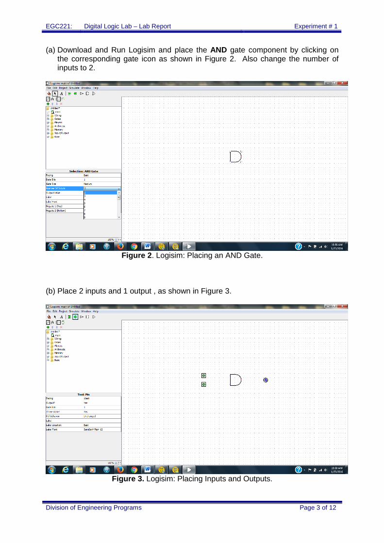
(a) Download and Run Logisim and place the AND gate component by clicking on the corresponding gate icon as shown in Figure 2. Also change the number of inputs to 2.
Figure 2. Logisim: Placing an AND Gate.
(b) Place 2 inputs and 1 output , as shown in Figure 3.
Figure 3. Logisim: Placing Inputs and Outputs.

EGC221: Digital Logic Lab – Lab Report Experiment # 1
Division of Engineering Programs Page 4 of 12
(c) Click on the Arrow and Place Wires, as shown in Figure 4.
Figure 4. Logisim: Placing Wires.
(d) Add Labels by first clicking on an entity, followed by filling in the label field, as
shown in figure 5.
Figure 5. Logisim: Placing Labels.
EGC221: Digital Logic Lab – Lab Report Experiment # 1
Division of Engineering Programs Page 5 of 12
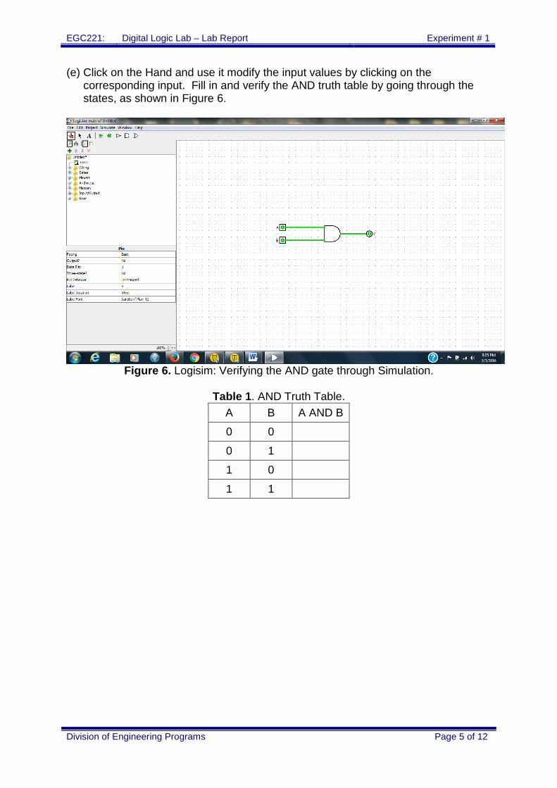
(e) Click on the Hand and use it modify the input values by clicking on the corresponding input. Fill in and verify the AND truth table by going through the states, as shown in Figure 6.
Figure 6. Logisim: Verifying the AND gate through Simulation.
Table 1. AND Truth Table.
A B A AND B
0 0
0 1
1 0
1 1
EGC221: Digital Logic Lab – Lab Report Experiment # 1
Division of Engineering Programs Page 6 of 12
(f) In LOGISIM place the OR gate circuit (with I/O) and verify its operation through Simulation. Complete Figure 7 and Table 2.
[Insert Logisim circuit here]
Figure 7. OR Gate Circuit.
Table 2. OR Truth Table. A B A OR B
0 0
0 1
1 0
1 1

EGC221: Digital Logic Lab – Lab Report Experiment # 1
Division of Engineering Programs Page 7 of 12
(g) In LOGISIM place the NOT gate circuit (with I/O) and verify its operation through Simulation. Complete Figure 8 and Table 3.
[Insert Logisim circuit here]
Figure 8. NOT Gate Circuit.
Table 3. NOT Truth Table. A NOT A
0
1
EGC221: Digital Logic Lab – Lab Report Experiment # 1
Division of Engineering Programs Page 8 of 12
(h) In LOGISIM place the XOR gate circuit (with I/O) and verify its operation through Simulation. Complete Figure 9 and Table 4.
[Insert Logisim circuit here]
Figure 9. XOR Gate Circuit.
Table 4. XOR Truth Table. A B A XOR B
0 0
0 1
1 0
1 1

EGC221: Digital Logic Lab – Lab Report Experiment # 1
Division of Engineering Programs Page 9 of 12
(i) In LOGISIM place the NAND gate circuit (with I/O) and verify its operation through Simulation. Complete Figure 10 and Table 5.
[Insert Logisim circuit here]
Figure 10. NAND Gate Circuit.
Table 5. NAND Truth Table. A B A NAND B
0 0
0 1
1 0
1 1

EGC221: Digital Logic Lab – Lab Report Experiment # 1
Division of Engineering Programs Page 10 of 12
(j) In LOGISIM place the NOR gate circuit (with I/O) and verify its operation through Simulation. Complete Figure 11 and Table 6.
[Insert Logisim circuit here]
Figure 11. NOR Gate Circuit.
Table 6. NOR Truth Table. A B A NOR B
0 0
0 1
1 0
1 1
EGC221: Digital Logic Lab – Lab Report Experiment # 1
Division of Engineering Programs Page 11 of 12
(k) In LOGISIM place the XNOR gate circuit (with I/O) and verify its operation through Simulation. Complete Figure 12 and Table 7.
[Insert Logisim circuit here]
Figure 12. XNOR Gate Circuit.
Table 7. XNOR Truth Table. A B A XNOR B
0 0
0 1
1 0
1 1
EGC221: Digital Logic Lab – Lab Report Experiment # 1
Division of Engineering Programs Page 12 of 12
Conclusions (discussion of results):


![Digital Logic LAB Manual KL-300 [Shorted]](https://static.fdocuments.net/doc/165x107/55cf93ef550346f57b9ed2c2/digital-logic-lab-manual-kl-300-shorted.jpg)