EFR32FG1 Flex Gecko Proprietary Protocol SoCFamily Data Sheet · EFR32FG1 Flex Gecko Proprietary...
179
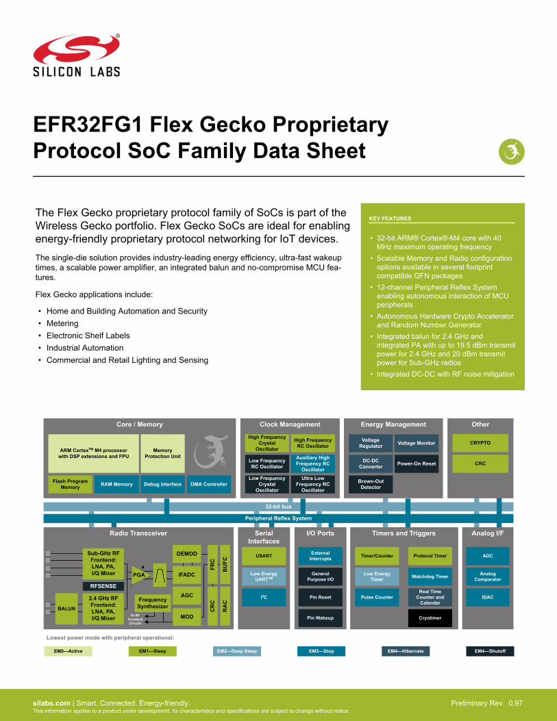
EFR32FG1 Flex Gecko Proprietary Protocol SoC Family Data Sheet The Flex Gecko proprietary protocol family of SoCs is part of the Wireless Gecko portfolio. Flex Gecko SoCs are ideal for enabling energy-friendly proprietary protocol networking for IoT devices. The single-die solution provides industry-leading energy efficiency, ultra-fast wakeup times, a scalable power amplifier, an integrated balun and no-compromise MCU fea- tures. Flex Gecko applications include: KEY FEATURES • 32-bit ARM® Cortex®-M4 core with 40 MHz maximum operating frequency • Scalable Memory and Radio configuration options available in several footprint compatible QFN packages • 12-channel Peripheral Reflex System enabling autonomous interaction of MCU peripherals • Autonomous Hardware Crypto Accelerator and Random Number Generator • Integrated balun for 2.4 GHz and integrated PA with up to 19.5 dBm transmit power for 2.4 GHz and 20 dBm transmit power for Sub-GHz radios • Integrated DC-DC with RF noise mitigation • Home and Building Automation and Security • Metering • Electronic Shelf Labels • Industrial Automation • Commercial and Retail Lighting and Sensing Timers and Triggers Real Time Counter and Calendar Cryotimer Timer/Counter Low Energy Timer Pulse Counter Watchdog Timer Protocol Timer 32-bit bus Peripheral Reflex System Serial Interfaces I/O Ports Analog I/F Lowest power mode with peripheral operational: USART Low Energy UART TM I 2 C External Interrupts General Purpose I/O Pin Reset Pin Wakeup ADC IDAC Analog Comparator Radio Transceiver DEMOD AGC IFADC CRC BUFC RFSENSE FRC RAC EM3—Stop EM2—Deep Sleep EM1—Sleep EM4—Hibernate EM4—Shutoff EM0—Active Core / Memory ARM Cortex TM M4 processor with DSP extensions and FPU Energy Management Brown-Out Detector DC-DC Converter Voltage Regulator Voltage Monitor Power-On Reset Other CRYPTO CRC Clock Management High Frequency Crystal Oscillator Low Frequency Crystal Oscillator Low Frequency RC Oscillator High Frequency RC Oscillator Ultra Low Frequency RC Oscillator Auxiliary High Frequency RC Oscillator Flash Program Memory RAM Memory Debug Interface DMA Controller Memory Protection Unit BALUN 2.4 GHz RF Frontend: LNA, PA, I/Q Mixer Sub-GHz RF Frontend: LNA, PA, I/Q Mixer PGA MOD To RF Frontend Circuits Frequency Synthesizer silabs.com | Smart. Connected. Energy-friendly. Preliminary Rev. 0.97 This information applies to a product under development. Its characteristics and specifications are subject to change without notice.
Transcript of EFR32FG1 Flex Gecko Proprietary Protocol SoCFamily Data Sheet · EFR32FG1 Flex Gecko Proprietary...
EFR32FG1 Flex Gecko Proprietary Protocol SoC Family Data Sheet
The Flex Gecko proprietary protocol family of SoCs is part of theWireless Gecko portfolio. Flex Gecko SoCs are ideal for enablingenergy-friendly proprietary protocol networking for IoT devices.The single-die solution provides industry-leading energy efficiency, ultra-fast wakeuptimes, a scalable power amplifier, an integrated balun and no-compromise MCU fea-tures.
Flex Gecko applications include:
KEY FEATURES
• 32-bit ARM® Cortex®-M4 core with 40MHz maximum operating frequency
• Scalable Memory and Radio configurationoptions available in several footprintcompatible QFN packages
• 12-channel Peripheral Reflex Systemenabling autonomous interaction of MCUperipherals
• Autonomous Hardware Crypto Acceleratorand Random Number Generator
• Integrated balun for 2.4 GHz andintegrated PA with up to 19.5 dBm transmitpower for 2.4 GHz and 20 dBm transmitpower for Sub-GHz radios
• Integrated DC-DC with RF noise mitigation
• Home and Building Automation and Security• Metering• Electronic Shelf Labels• Industrial Automation• Commercial and Retail Lighting and Sensing
Timers and Triggers
Real Time Counter and
Calendar
Cryotimer
Timer/Counter
Low Energy Timer
Pulse Counter
Watchdog Timer
Protocol Timer
32-bit bus
Peripheral Reflex System
Serial Interfaces
I/O Ports Analog I/F
Lowest power mode with peripheral operational:
USART
Low Energy UARTTM
I2C
External Interrupts
General Purpose I/O
Pin Reset
Pin Wakeup
ADC
IDAC
Analog Comparator
Radio Transceiver
DEMOD
AGC
IFADC
CR
C
BU
FC
RFSENSE
FRC
RA
C
EM3—StopEM2—Deep SleepEM1—Sleep EM4—Hibernate EM4—ShutoffEM0—Active
Core / Memory
ARM CortexTM M4 processorwith DSP extensions and FPU
Energy Management
Brown-Out Detector
DC-DC Converter
Voltage Regulator Voltage Monitor
Power-On Reset
Other
CRYPTO
CRC
Clock Management
High Frequency Crystal
Oscillator
Low Frequency Crystal
Oscillator
Low FrequencyRC Oscillator
High FrequencyRC Oscillator
Ultra Low Frequency RC
Oscillator
Auxiliary High Frequency RC
Oscillator
Flash Program Memory RAM Memory Debug Interface DMA Controller
Memory Protection Unit
BALUN
2.4 GHz RF Frontend:LNA, PA, I/Q Mixer
Sub-GHz RF Frontend:LNA, PA, I/Q Mixer PGA
MODTo RF Frontend Circuits
Frequency Synthesizer
silabs.com | Smart. Connected. Energy-friendly. Preliminary Rev. 0.97 This information applies to a product under development. Its characteristics and specifications are subject to change without notice.
1. Feature List
The EFR32FG1 highlighted features are listed below.• Low Power Wireless System-on-Chip.
• High Performance 32-bit 40 MHz ARM Cortex®-M4 withDSP instruction and floating-point unit for efficient signalprocessing
• Up to 256 kB flash program memory• Up to 32 kB RAM data memory• 2.4 GHz and Sub-GHz radio operation• Transmit power:
• 2.4 GHz radio: Up to 19.5 dBm• Sub-GHz radio: Up to 20 dBm
• Low Energy Consumption• 8.7 mA RX current at 2.4 GHz• 8.2 mA TX current @ 0 dBm output power at 2.4 GHz• 8.1 mA RX current at 868 MHz• 34.5 mA TX current @ 14 dBm output power at 868 MHz• 63 μA/MHz in Active Mode (EM0)• 1.4 μA EM2 DeepSleep current (full RAM retention and
RTCC running from LFXO)• 0.58 μA EM4H Hibernate Mode (128 byte RAM retention)• Wake on Radio with signal strength detection, preamble
pattern detection, frame detection and timeout• High Receiver Performance
• -94 dBm sensitivity @ 1 Mbit/s GFSK (2.4GHz)• -121.4 dBm sensitivity at 2.4 kbps GFSK (868 MHz)
• Supported Modulation Formats• 2-FSK / 4-FSK with fully configurable shaping• Shaped OQPSK / (G)MSK• Configurable DSSS and FEC• BPSK / DBPSK TX• OOK / ASK
• Supported Protocols:• Proprietary Protocols• Wireless M-Bus• Low Power Wide Area Networks
• Support for Internet Security• General Purpose CRC• Random Number Generation• Hardware Cryptographic Acceleration for AES 128/256,
SHA-1, SHA-2 (SHA-224 and SHA-256) and ECC
• Wide selection of MCU peripherals• 12-bit 1 Msps SAR Analog to Digital Converter (ADC)• 2× Analog Comparator (ACMP)• Digital to Analog Current Converter (IDAC)• Up to 32 pins connected to analog channels (APORT)
shared between Analog Comparators, ADC, and IDAC• Up to 32 General Purpose I/O pins with output state reten-
tion and asynchronous interrupts• 8 Channel DMA Controller• 12 Channel Peripheral Reflex System (PRS)• 2×16-bit Timer/Counter
• 3 + 4 Compare/Capture/PWM channels• 32-bit Real Time Counter and Calendar• 16-bit Low Energy Timer for waveform generation• 32-bit Ultra Low Energy Timer/Counter for periodic wake-up
from any Energy Mode• 16-bit Pulse Counter with asynchronous operation• Watchdog Timer with dedicated RC oscillator @ 50nA• 2×Universal Synchronous/Asynchronous Receiver/Trans-
mitter (UART/SPI/SmartCard (ISO 7816)/IrDA/I2S)• Low Energy UART (LEUART™)• I2C interface with SMBus support and address recognition
in EM3 Stop• Wide Operating Range
• 1.85 V to 3.8 V single power supply• Integrated DC-DC, down to 1.8 V output with up to 200 mA
load current for system• -40 °C to 85 °C
• QFN32 5x5 mm Package• QFN48 7x7 mm Package
EFR32FG1 Flex Gecko Proprietary Protocol SoCFamily Data SheetFeature List
silabs.com | Smart. Connected. Energy-friendly. Preliminary Rev. 0.97 | 1
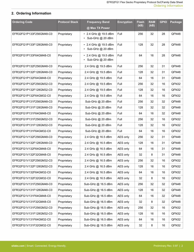
2. Ordering Information
Ordering Code Protocol Stack Frequency Band
@ Max TX Power
Encryption Flash(kB)
RAM(kB)
GPIO Package
EFR32FG1P133F256GM48-C0 Proprietary • 2.4 GHz @ 19.5 dBm• Sub-GHz @ 20 dBm
Full 256 32 28 QFN48
EFR32FG1P133F128GM48-C0 Proprietary • 2.4 GHz @ 19.5 dBm• Sub-GHz @ 20 dBm
Full 128 32 28 QFN48
EFR32FG1P133F64GM48-C0 Proprietary • 2.4 GHz @ 19.5 dBm• Sub-GHz @ 20 dBm
Full 64 16 28 QFN48
EFR32FG1P132F256GM48-C0 Proprietary 2.4 GHz @ 19.5 dBm Full 256 32 31 QFN48
EFR32FG1P132F128GM48-C0 Proprietary 2.4 GHz @ 19.5 dBm Full 128 32 31 QFN48
EFR32FG1P132F64GM48-C0 Proprietary 2.4 GHz @ 19.5 dBm Full 64 16 31 QFN48
EFR32FG1P132F256GM32-C0 Proprietary 2.4 GHz @ 19.5 dBm Full 256 32 16 QFN32
EFR32FG1P132F128GM32-C0 Proprietary 2.4 GHz @ 19.5 dBm Full 128 32 16 QFN32
EFR32FG1P132F64GM32-C0 Proprietary 2.4 GHz @ 19.5 dBm Full 64 16 16 QFN32
EFR32FG1P131F256GM48-C0 Proprietary Sub-GHz @ 20 dBm Full 256 32 32 QFN48
EFR32FG1P131F128GM48-C0 Proprietary Sub-GHz @ 20 dBm Full 128 32 32 QFN48
EFR32FG1P131F64GM48-C0 Proprietary Sub-GHz @ 20 dBm Full 64 16 32 QFN48
EFR32FG1P131F256GM32-C0 Proprietary Sub-GHz @ 20 dBm Full 256 32 16 QFN32
EFR32FG1P131F128GM32-C0 Proprietary Sub-GHz @ 20 dBm Full 128 32 16 QFN32
EFR32FG1P131F64GM32-C0 Proprietary Sub-GHz @ 20 dBm Full 64 16 16 QFN32
EFR32FG1V132F256GM48-C0 Proprietary 2.4 GHz @ 16.5 dBm AES only 256 32 31 QFN48
EFR32FG1V132F128GM48-C0 Proprietary 2.4 GHz @ 16.5 dBm AES only 128 16 31 QFN48
EFR32FG1V132F64GM48-C0 Proprietary 2.4 GHz @ 16.5 dBm AES only 64 16 31 QFN48
EFR32FG1V132F32GM48-C0 Proprietary 2.4 GHz @ 16.5 dBm AES only 32 8 31 QFN48
EFR32FG1V132F256GM32-C0 Proprietary 2.4 GHz @ 16.5 dBm AES only 256 32 16 QFN32
EFR32FG1V132F128GM32-C0 Proprietary 2.4 GHz @ 16.5 dBm AES only 128 16 16 QFN32
EFR32FG1V132F64GM32-C0 Proprietary 2.4 GHz @ 16.5 dBm AES only 64 16 16 QFN32
EFR32FG1V132F32GM32-C0 Proprietary 2.4 GHz @ 16.5 dBm AES only 32 8 16 QFN32
EFR32FG1V131F256GM48-C0 Proprietary Sub-GHz @ 16.5 dBm AES only 256 32 32 QFN48
EFR32FG1V131F128GM48-C0 Proprietary Sub-GHz @ 16.5 dBm AES only 128 16 32 QFN48
EFR32FG1V131F64GM48-C0 Proprietary Sub-GHz @ 16.5 dBm AES only 64 16 32 QFN48
EFR32FG1V131F32GM48-C0 Proprietary Sub-GHz @ 16.5 dBm AES only 32 8 32 QFN48
EFR32FG1V131F256GM32-C0 Proprietary Sub-GHz @ 16.5 dBm AES only 256 32 16 QFN32
EFR32FG1V131F128GM32-C0 Proprietary Sub-GHz @ 16.5 dBm AES only 128 16 16 QFN32
EFR32FG1V131F64GM32-C0 Proprietary Sub-GHz @ 16.5 dBm AES only 64 16 16 QFN32
EFR32FG1V131F32GM32-C0 Proprietary Sub-GHz @ 16.5 dBm AES only 32 8 16 QFN32
EFR32FG1 Flex Gecko Proprietary Protocol SoCFamily Data SheetOrdering Information
silabs.com | Smart. Connected. Energy-friendly. Preliminary Rev. 0.97 | 2
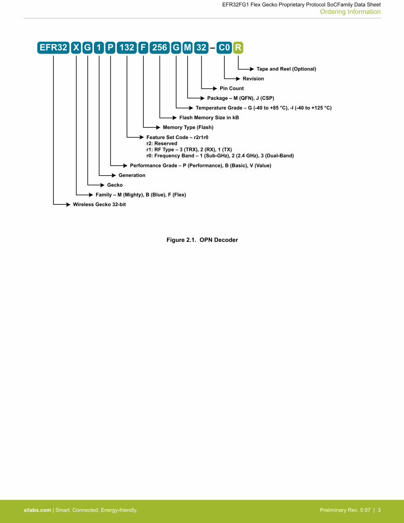
EFR32 –1 P F G C0 R
Tape and Reel (Optional)
Revision
Pin Count
Package – M (QFN), J (CSP)
Flash Memory Size in kB
Memory Type (Flash)
Feature Set Code – r2r1r0r2: Reservedr1: RF Type – 3 (TRX), 2 (RX), 1 (TX)r0: Frequency Band – 1 (Sub-GHz), 2 (2.4 GHz), 3 (Dual-Band)
GX 132 256 M 32
Temperature Grade – G (-40 to +85 °C), -I (-40 to +125 °C)
Performance Grade – P (Performance), B (Basic), V (Value)
Generation
Family – M (Mighty), B (Blue), F (Flex)
Wireless Gecko 32-bit
Gecko
Figure 2.1. OPN Decoder
EFR32FG1 Flex Gecko Proprietary Protocol SoCFamily Data SheetOrdering Information
silabs.com | Smart. Connected. Energy-friendly. Preliminary Rev. 0.97 | 3
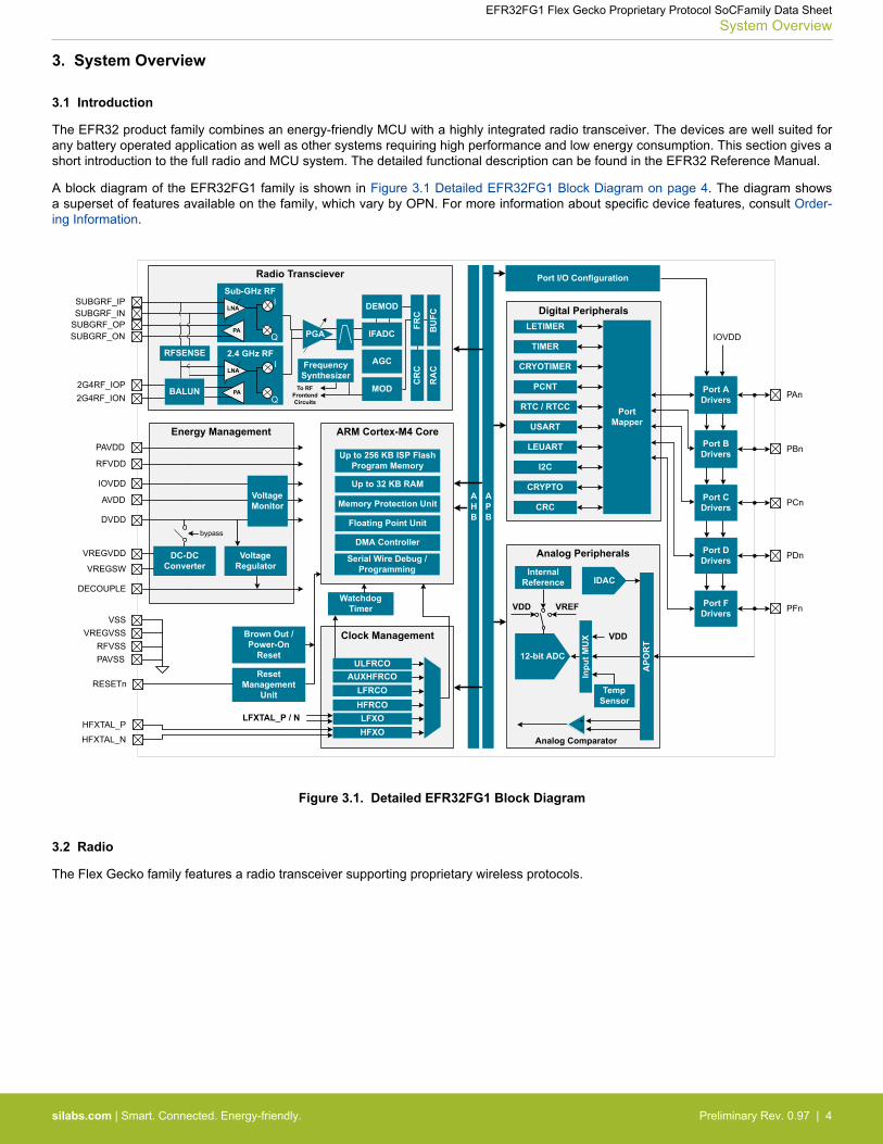
3. System Overview
3.1 Introduction
The EFR32 product family combines an energy-friendly MCU with a highly integrated radio transceiver. The devices are well suited forany battery operated application as well as other systems requiring high performance and low energy consumption. This section gives ashort introduction to the full radio and MCU system. The detailed functional description can be found in the EFR32 Reference Manual.
A block diagram of the EFR32FG1 family is shown in Figure 3.1 Detailed EFR32FG1 Block Diagram on page 4. The diagram showsa superset of features available on the family, which vary by OPN. For more information about specific device features, consult Order-ing Information.
Analog Peripherals
Clock Management
LFXTAL_P / N LFXO
IDAC
ARM Cortex-M4 Core
Up to 256 KB ISP FlashProgram Memory
Up to 32 KB RAMAHB
Watchdog Timer
Reset Management
Unit
Brown Out / Power-On
Reset
RESETn
Digital Peripherals
Inpu
t MU
X
Port Mapper
Port I/O Configuration
I2C
Analog Comparator
12-bit ADC
Temp Sensor
VREFVDD
VDD
Internal Reference
TIMER
CRYOTIMER
PCNT
USART
Port ADrivers
Port B Drivers
PAn
Port C Drivers PCn
PBn
Port D Drivers PDn
LETIMER
RTC / RTCC
IOVDD
AUXHFRCO
HFRCO
ULFRCO
HFXO
Port F Drivers PFn
Memory Protection Unit
LFRCO
APB
LEUART
CRYPTO
CRC
DMA Controller
+-
APO
RT
Floating Point Unit
Energy Management
DC-DC Converter
DVDD
VREGVDD
VSS
VREGSW
bypass
AVDD
PAVDD
RFVDD
Voltage Regulator
DECOUPLE
IOVDDVoltage Monitor
VREGVSSRFVSSPAVSS
Serial Wire Debug / Programming
Radio Transciever
2G4RF_IOP2G4RF_ION
2.4 GHz RF
PA
I
Q
LNAFrequency
Synthesizer
DEMOD
AGC
IFADC
CR
C
BU
FC
MOD
FRC
RA
C
PGA
HFXTAL_P
HFXTAL_N
SUBGRF_OPSUBGRF_ON
Sub-GHz RFI
QPA
SUBGRF_IPSUBGRF_IN
LNA
To RF Frontend Circuits
BALUN
RFSENSE
Figure 3.1. Detailed EFR32FG1 Block Diagram
3.2 Radio
The Flex Gecko family features a radio transceiver supporting proprietary wireless protocols.
EFR32FG1 Flex Gecko Proprietary Protocol SoCFamily Data SheetSystem Overview
silabs.com | Smart. Connected. Energy-friendly. Preliminary Rev. 0.97 | 4
3.2.1 Antenna Interface
The EFR32FG1 family includes devices which support both single-band and dual-band RF communication over separate physical RFinterfaces.
The 2.4 GHz antenna interface consists of two pins (2G4RF_IOP and 2G4RF_ION) that interface directly to the on-chip BALUN. The2G4RF_ION pin should be grounded externally.
The sub-GHz antenna interface consists of a differential transmit interface (pins SUBGRF_OP and SUBGRF_ON) and a differential re-ceive interface (pinsSUBGRF_IP and SUBGRF_IN).
The external components and power supply connections for the antenna interface typical applications are shown in the RF MatchingNetworks section.
3.2.2 Fractional-N Frequency Synthesizer
The EFR32FG1 contains a high performance, low phase noise, fully integrated fractional-N frequency synthesizer. The synthesizer isused in receive mode to generate the LO frequency used by the down-conversion mixer. It is also used in transmit mode to directlygenerate the modulated RF carrier.
The fractional-N architecture provides excellent phase noise performance combined with frequency resolution better than 100 Hz, withlow energy consumption. The synthesizer has fast frequency settling which allows very short receiver and transmitter wake up times tooptimize system energy consumption.
3.2.3 Receiver Architecture
The EFR32FG1 uses a low-IF receiver architecture, consisting of a Low-Noise Amplifier (LNA) followed by an I/Q down-conversion mix-er, employing a crystal reference. The I/Q signals are further filtered and amplified before being sampled by the IF analog-to-digitalconverter (IFADC).
The IF frequency is configurable from 150 kHz to 1371 kHz. The IF can further be configured for high-side or low-side injection, provid-ing flexibility with respect to known interferers at the image frequency.
The Automatic Gain Control (AGC) module adjusts the receiver gain to optimize performance and avoid saturation for excellent selec-tivity and blocking performance. The 2.4 GHz radio is calibrated at production to improve image rejection performance. The sub-GHzradio can be calibrated on-demand by the user for the desired frequency band.
Demodulation is performed in the digital domain. The demodulator performs configurable decimation and channel filtering to allow re-ceive bandwidths ranging from 0.1 to 2530 kHz. High carrier frequency and baud rate offsets are tolerated by active estimation andcompensation. Advanced features supporting high quality communication under adverse conditions include forward error correction byblock and convolutional coding as well as Direct Sequence Spread Spectrum (DSSS).
A Received Signal Strength Indicator (RSSI) is available for signal quality metrics, for level-based proximity detection, and for RF chan-nel access by Collision Avoidance (CA) or Listen Before Talk (LBT) algorithms. An RSSI capture value is associated with each receivedframe and the dynamic RSSI measurement can be monitored throughout reception.
The EFR32FG1 features integrated support for antenna diversity to improve link budget for 802.15.4 DSSS-OQPSK PHY configurationin the 2.4GHz band, using complementary control outputs to an external switch. Internal configurable hardware controls automaticswitching between antennae during RF receive detection operations.
3.2.4 Transmitter Architecture
The EFR32FG1 uses a direct-conversion transmitter architecture. For constant envelope modulation formats, the modulator controlsphase and frequency modulation in the frequency synthesizer. Transmit symbols or chips are optionally shaped by a digital shapingfilter. The shaping filter is fully configurable, including the BT product, and can be used to implement Gaussian or Raised Cosine shap-ing.
Carrier Sense Multiple Access - Collision Avoidance (CSMA-CA) or Listen Before Talk (LBT) algorithms can be automatically timed bythe EFR32FG1. These algorithms are typically defined by regulatory standards to improve inter-operability in a given bandwidth be-tween devices that otherwise lack synchronized RF channel access.
3.2.5 Wake on Radio
The Wake on Radio feature allows flexible, autonomous RF sensing, qualification, and demodulation without required MCU activity, us-ing a subsystem of the EFR32FG1 including the Radio Controller (RAC), Peripheral Reflex System (PRS), and Low Energy peripherals.
EFR32FG1 Flex Gecko Proprietary Protocol SoCFamily Data SheetSystem Overview
silabs.com | Smart. Connected. Energy-friendly. Preliminary Rev. 0.97 | 5
3.2.6 RFSENSE
The RFSENSE module generates a system wakeup interrupt upon detection of wideband RF energy at the antenna interface, providingtrue RF wakeup capabilities from low energy modes including EM2, EM3 and EM4.
RFSENSE triggers on a relatively strong RF signal and is available in the lowest energy modes, allowing exceptionally low energy con-sumption. RFSENSE does not demodulate or otherwise qualify the received signal, but software may respond to the wakeup event byenabling normal RF reception.
Various strategies for optimizing power consumption and system response time in presence of false alarms may be employed usingavailable timer peripherals.
3.2.7 Flexible Frame Handling
EFR32FG1 has an extensive and flexible frame handling support for easy implementation of even complex communication protocols.The Frame Controller (FRC) supports all low level and timing critical tasks together with the Radio Controller and Modulator/Demodula-tor:• Highly adjustable preamble length• Up to 2 simultaneous synchronization words, each up to 32 bits and providing separate interrupts• Frame disassembly and address matching (filtering) to accept or reject frames• Automatic ACK frame assembly and transmission• Fully flexible CRC generation and verification:
• Multiple CRC values can be embedded in a single frame• 8, 16, 24 or 32-bit CRC value• Configurable CRC bit and byte ordering
• Selectable bit-ordering (least significant or most significant bit first)• Optional data whitening• Optional Forward Error Correction (FEC), including convolutional encoding / decoding and block encoding / decoding• Half rate convolutional encoder and decoder with constraint lengths from 2 to 7 and optional puncturing• Optional symbol interleaving, typically used in combination with FEC• Symbol coding, such as Manchester or DSSS, or biphase space encoding using FEC hardware• UART encoding over air, with start and stop bit insertion / removal• Test mode support, such as modulated or unmodulated carrier output• Received frame timestamping
3.2.8 Packet and State Trace
The EFR32FG1 Frame Controller has a packet and state trace unit that provides valuable information during the development phase. Itfeatures:• Non-intrusive trace of transmit data, receive data and state information• Data observability on a single-pin UART data output, or on a two-pin SPI data output• Configurable data output bitrate / baudrate• Multiplexed transmitted data, received data and state / meta information in a single serial data stream
3.2.9 Data Buffering
The EFR32FG1 features an advanced Radio Buffer Controller (BUFC) capable of handling up to 4 buffers of adjustable size from 64bytes to 4096 bytes. Each buffer can be used for RX, TX or both. The buffer data is located in RAM, enabling zero-copy operations.
3.2.10 Radio Controller (RAC)
The Radio Controller controls the top level state of the radio subsystem in the EFR32FG1. It performs the following tasks:• Precisely-timed control of enabling and disabling of the receiver and transmitter circuitry• Run-time calibration of receiver, transmitter and frequency synthesizer• Detailed frame transmission timing, including optional LBT or CSMA-CA
EFR32FG1 Flex Gecko Proprietary Protocol SoCFamily Data SheetSystem Overview
silabs.com | Smart. Connected. Energy-friendly. Preliminary Rev. 0.97 | 6

3.2.11 Random Number Generator
The Frame Controller (FRC) implements a random number generator that uses entropy gathered from noise in the RF receive chain.The data is suitable for use in cryptographic applications.
Output from the random number generator can be used either directly or as a seed or entropy source for software-based random num-ber generator algorithms such as Fortuna.
EFR32FG1 Flex Gecko Proprietary Protocol SoCFamily Data SheetSystem Overview
silabs.com | Smart. Connected. Energy-friendly. Preliminary Rev. 0.97 | 7
3.3 Power
The EFR32FG1 has an Energy Management Unit (EMU) and efficient integrated regulators to generate internal supply voltages. Only asingle external supply voltage is required, from which all internal voltages are created. An optional integrated DC-DC buck regulator canbe utilized to further reduce the current consumption. The DC-DC regulator requires one external inductor and one external capacitor.
AVDD and VREGVDD need to be 1.85 V or higher for the MCU to operate across all conditions; however the rest of the system willoperate down to 1.62 V, including the digital supply and I/O. This means that the device is fully compatible with 1.8 V components.Running from a sufficiently high supply, the device can use the DC-DC to regulate voltage not only for itself, but also for other PCBcomponents, supplying up to a total of 200 mA.
3.3.1 Energy Management Unit (EMU)
The Energy Management Unit manages transitions of energy modes in the device. Each energy mode defines which peripherals andfeatures are available and the amount of current the device consumes. The EMU can also be used to turn off the power to unused RAMblocks, and it contains control registers for the dc-dc regulator and the Voltage Monitor (VMON). The VMON is used to monitor multiplesupply voltages. It has multiple channels which can be programmed individually by the user to determine if a sensed supply has fallenbelow a chosen threshold.
3.3.2 DC-DC Converter
The DC-DC buck converter covers a wide range of load currents and provides up to 90% efficiency in energy modes EM0, EM1, EM2and EM3, and can supply up to 200 mA to the device and surrounding PCB components. Patented RF noise mitigation allows operationof the DC-DC converter without degrading sensitivity of radio components. Protection features include programmable current limiting,short-circuit protection, and dead-time protection. The DC-DC converter may also enter bypass mode when the input voltage is too lowfor efficient operation. In bypass mode, the DC-DC input supply is internally connected directly to its output through a low resistanceswitch. Bypass mode also supports in-rush current limiting to prevent input supply voltage droops due to excessive output current tran-sients.
3.4 General Purpose Input/Output (GPIO)
EFR32FG1 has up to 32 General Purpose Input/Output pins. Each GPIO pin can be individually configured as either an output or input.More advanced configurations including open-drain, open-source, and glitch-filtering can be configured for each individual GPIO pin.The GPIO pins can be overridden by peripheral connections, like SPI communication. Each peripheral connection can be routed to sev-eral GPIO pins on the device. The input value of a GPIO pin can be routed through the Peripheral Reflex System to other peripherals.The GPIO subsystem supports asynchronous external pin interrupts.
3.5 Clocking
3.5.1 Clock Management Unit (CMU)
The Clock Management Unit controls oscillators and clocks in the EFR32FG1. Individual enabling and disabling of clocks to all periph-eral modules is performed by the CMU. The CMU also controls enabling and configuration of the oscillators. A high degree of flexibilityallows software to optimize energy consumption in any specific application by minimizing power dissipation in unused peripherals andoscillators.
3.5.2 Internal and External Oscillators
The EFR32FG1 supports two crystal oscillators and fully integrates four RC oscillators, listed below.• A high frequency crystal oscillator (HFXO) with integrated load capacitors, tunable in small steps, provides a precise timing refer-
ence for the MCU. Crystal frequencies in the range from 38 to 40 MHz are supported. An external clock source such as a TCXO canalso be applied to the HFXO input for improved accuracy over temperature.
• A 32.768 kHz crystal oscillator (LFXO) provides an accurate timing reference for low energy modes.• An integrated high frequency RC oscillator (HFRCO) is available for the MCU system, when crystal accuracy is not required. The
HFRCO employs fast startup at minimal energy consumption combined with a wide frequency range.• An integrated auxilliary high frequency RC oscillator (AUXHFRCO) is available for timing the general-purpose ADC and the Serial
Wire debug port with a wide frequency range.• An integrated low frequency 32.768 kHz RC oscillator (LFRCO) can be used as a timing reference in low energy modes, when crys-
tal accuracy is not required.• An integrated ultra-low frequency 1 kHz RC oscillator (ULFRCO) is available to provide a timing reference at the lowest energy con-
sumption in low energy modes.
EFR32FG1 Flex Gecko Proprietary Protocol SoCFamily Data SheetSystem Overview
silabs.com | Smart. Connected. Energy-friendly. Preliminary Rev. 0.97 | 8
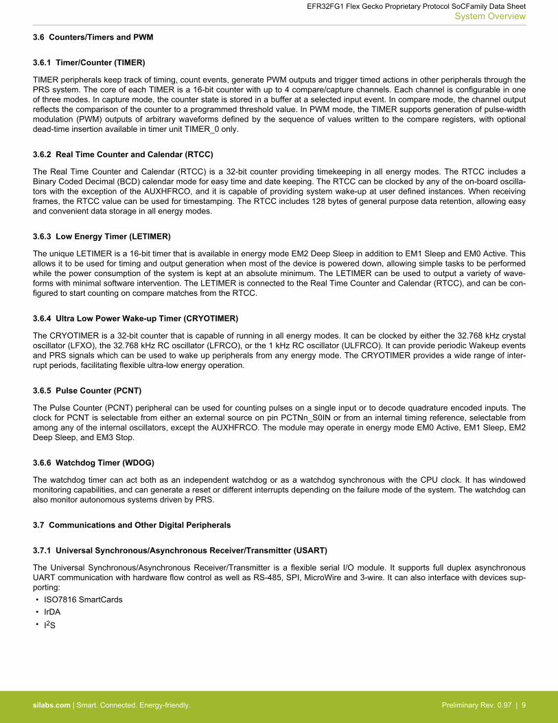
3.6 Counters/Timers and PWM
3.6.1 Timer/Counter (TIMER)
TIMER peripherals keep track of timing, count events, generate PWM outputs and trigger timed actions in other peripherals through thePRS system. The core of each TIMER is a 16-bit counter with up to 4 compare/capture channels. Each channel is configurable in oneof three modes. In capture mode, the counter state is stored in a buffer at a selected input event. In compare mode, the channel outputreflects the comparison of the counter to a programmed threshold value. In PWM mode, the TIMER supports generation of pulse-widthmodulation (PWM) outputs of arbitrary waveforms defined by the sequence of values written to the compare registers, with optionaldead-time insertion available in timer unit TIMER_0 only.
3.6.2 Real Time Counter and Calendar (RTCC)
The Real Time Counter and Calendar (RTCC) is a 32-bit counter providing timekeeping in all energy modes. The RTCC includes aBinary Coded Decimal (BCD) calendar mode for easy time and date keeping. The RTCC can be clocked by any of the on-board oscilla-tors with the exception of the AUXHFRCO, and it is capable of providing system wake-up at user defined instances. When receivingframes, the RTCC value can be used for timestamping. The RTCC includes 128 bytes of general purpose data retention, allowing easyand convenient data storage in all energy modes.
3.6.3 Low Energy Timer (LETIMER)
The unique LETIMER is a 16-bit timer that is available in energy mode EM2 Deep Sleep in addition to EM1 Sleep and EM0 Active. Thisallows it to be used for timing and output generation when most of the device is powered down, allowing simple tasks to be performedwhile the power consumption of the system is kept at an absolute minimum. The LETIMER can be used to output a variety of wave-forms with minimal software intervention. The LETIMER is connected to the Real Time Counter and Calendar (RTCC), and can be con-figured to start counting on compare matches from the RTCC.
3.6.4 Ultra Low Power Wake-up Timer (CRYOTIMER)
The CRYOTIMER is a 32-bit counter that is capable of running in all energy modes. It can be clocked by either the 32.768 kHz crystaloscillator (LFXO), the 32.768 kHz RC oscillator (LFRCO), or the 1 kHz RC oscillator (ULFRCO). It can provide periodic Wakeup eventsand PRS signals which can be used to wake up peripherals from any energy mode. The CRYOTIMER provides a wide range of inter-rupt periods, facilitating flexible ultra-low energy operation.
3.6.5 Pulse Counter (PCNT)
The Pulse Counter (PCNT) peripheral can be used for counting pulses on a single input or to decode quadrature encoded inputs. Theclock for PCNT is selectable from either an external source on pin PCTNn_S0IN or from an internal timing reference, selectable fromamong any of the internal oscillators, except the AUXHFRCO. The module may operate in energy mode EM0 Active, EM1 Sleep, EM2Deep Sleep, and EM3 Stop.
3.6.6 Watchdog Timer (WDOG)
The watchdog timer can act both as an independent watchdog or as a watchdog synchronous with the CPU clock. It has windowedmonitoring capabilities, and can generate a reset or different interrupts depending on the failure mode of the system. The watchdog canalso monitor autonomous systems driven by PRS.
3.7 Communications and Other Digital Peripherals
3.7.1 Universal Synchronous/Asynchronous Receiver/Transmitter (USART)
The Universal Synchronous/Asynchronous Receiver/Transmitter is a flexible serial I/O module. It supports full duplex asynchronousUART communication with hardware flow control as well as RS-485, SPI, MicroWire and 3-wire. It can also interface with devices sup-porting:• ISO7816 SmartCards• IrDA• I2S
EFR32FG1 Flex Gecko Proprietary Protocol SoCFamily Data SheetSystem Overview
silabs.com | Smart. Connected. Energy-friendly. Preliminary Rev. 0.97 | 9
3.7.2 Low Energy Universal Asynchronous Receiver/Transmitter (LEUART)
The unique LEUARTTM provides two-way UART communication on a strict power budget. Only a 32.768 kHz clock is needed to allowUART communication up to 9600 baud. The LEUART includes all necessary hardware to make asynchronous serial communicationpossible with a minimum of software intervention and energy consumption.
3.7.3 Inter-Integrated Circuit Interface (I2C)
The I2C module provides an interface between the MCU and a serial I2C bus. It is capable of acting as both a master and a slave andsupports multi-master buses. Standard-mode, fast-mode and fast-mode plus speeds are supported, allowing transmission rates from 10kbit/s up to 1 Mbit/s. Slave arbitration and timeouts are also available, allowing implementation of an SMBus-compliant system. Theinterface provided to software by the I2C module allows precise timing control of the transmission process and highly automated trans-fers. Automatic recognition of slave addresses is provided in active and low energy modes.
3.7.4 Peripheral Reflex System (PRS)
The Peripheral Reflex System provides a communication network between different peripheral modules without software involvement.Peripheral modules producing Reflex signals are called producers. The PRS routes Reflex signals from producers to consumer periph-erals which in turn perform actions in response. Edge triggers and other functionality can be applied by the PRS. The PRS allows pe-ripheral to act autonomously without waking the MCU core, saving power.
3.8 Security Features
3.8.1 GPCRC (General Purpose Cyclic Redundancy Check)
The GPCRC module implements a Cyclic Redundancy Check (CRC) function. It supports both 32-bit and 16-bit polynomials. The sup-ported 32-bit polynomial is 0x04C11DB7 (IEEE 802.3), while the 16-bit polynomial can be programmed to any value, depending on theneeds of the application.
3.8.2 Crypto Accelerator (CRYPTO)
The Crypto Accelerator is a fast and energy-efficient autonomous hardware encryption and decryption accelerator. EFR32 devices sup-port various levels of hardware-accelerated encryption, depending on the part number. The Ordering Information Table specifies wheth-er this part has full or AES-only crypto support. AES-only devices support AES encryption and decryption with 128- or 256-bit keys.Full crypto support adds ECC over both GF(P) and GF(2m), SHA-1 and SHA-2 (SHA-224 and SHA-256).
Supported block cipher modes of operation for AES include: ECB, CTR, CBC, PCBC, CFB, OFB, GCM, CBC-MAC, GMAC and CCM.
Supported ECC NIST recommended curves include P-192, P-224, P-256, K-163, K-233, B-163 and B-233.
The CRYPTO is tightly linked to the Radio Buffer Controller (BUFC) enabling fast and efficient autonomous cipher operations on databuffer content. It allows fast processing of GCM (AES), ECC and SHA with little CPU intervention. CRYPTO also provides trigger sig-nals for DMA read and write operations.
3.9 Analog
3.9.1 Analog Port (APORT)
The Analog Port (APORT) is an analog interconnect matrix allowing access to analog modules ADC, ACMP, and IDAC on a flexibleselection of pins. Each APORT bus consists of analog switches connected to a common wire. Since many clients can operate differen-tially, buses are grouped by X/Y pairs.
3.9.2 Analog Comparator (ACMP)
The Analog Comparator is used to compare the voltage of two analog inputs, with a digital output indicating which input voltage is high-er. Inputs are selected from among internal references and external pins. The tradeoff between response time and current consumptionis configurable by software. Two 6-bit reference dividers allow for a wide range of internally-programmable reference sources. TheACMP can also be used to monitor the supply voltage. An interrupt can be generated when the supply falls below or rises above theprogrammable threshold.
EFR32FG1 Flex Gecko Proprietary Protocol SoCFamily Data SheetSystem Overview
silabs.com | Smart. Connected. Energy-friendly. Preliminary Rev. 0.97 | 10

3.9.3 Analog to Digital Converter (ADC)
The ADC is a Successive Approximation Register (SAR) architecture, with a resolution of up to 12 bits at up to 1 MSamples/s. Theoutput sample resolution is configurable and additional resolution is possible using integrated hardware for averaging over multiplesamples. The ADC includes integrated voltage references and an integrated temperature sensor. Inputs are selectable from a widerange of sources, including pins configurable as either single-ended or differential.
3.9.4 Digital to Analog Current Converter (IDAC)
The Digital to Analog Current Converter can source or sink a configurable constant current. This current can be driven on an output pinor routed to the selected ADC input pin for capacitive sensing. The current is programmable between 0.05 µA and 64 µA with severalranges with various step sizes.
3.10 Reset Management Unit (RMU)
The RMU is responsible for handling reset of the EFR32FG1. A wide range of reset sources are available, including several powersupply monitors, pin reset, software controlled reset, core lockup reset and watchdog reset.
3.11 Core and Memory
3.11.1 Processor Core
The ARM Cortex-M processor includes a 32-bit RISC processor integrating the following features and tasks in the system:• ARM Cortex-M4 RISC processor achieving 1.25 Dhrystone MIPS/MHz• Memory Protection Unit (MPU) supporting up to 8 memory segments• Up to 256 kB flash program memory• Up to 32 kB RAM data memory• Configuration and event handling of all modules• 2-pin Serial-Wire debug interface
3.11.2 Memory System Controller (MSC)
The Memory System Controller (MSC) is the program memory unit of the microcontroller. The flash memory is readable and writablefrom both the Cortex-M and DMA. The flash memory is divided into two blocks; the main block and the information block. Program codeis normally written to the main block, whereas the information block is available for special user data and flash lock bits. There is also aread-only page in the information block containing system and device calibration data. Read and write operations are supported in en-ergy modes EM0 Active and EM1 Sleep.
3.11.3 Linked Direct Memory Access Controller (LDMA)
The Linked Direct Memory Access (LDMA) controller features 8 channels capable of performing memory operations independently ofsoftware. This reduces both energy consumption and software workload. The LDMA allows operations to be linked together and stag-ed, enabling sophisticated operations to be implemented.
EFR32FG1 Flex Gecko Proprietary Protocol SoCFamily Data SheetSystem Overview
silabs.com | Smart. Connected. Energy-friendly. Preliminary Rev. 0.97 | 11
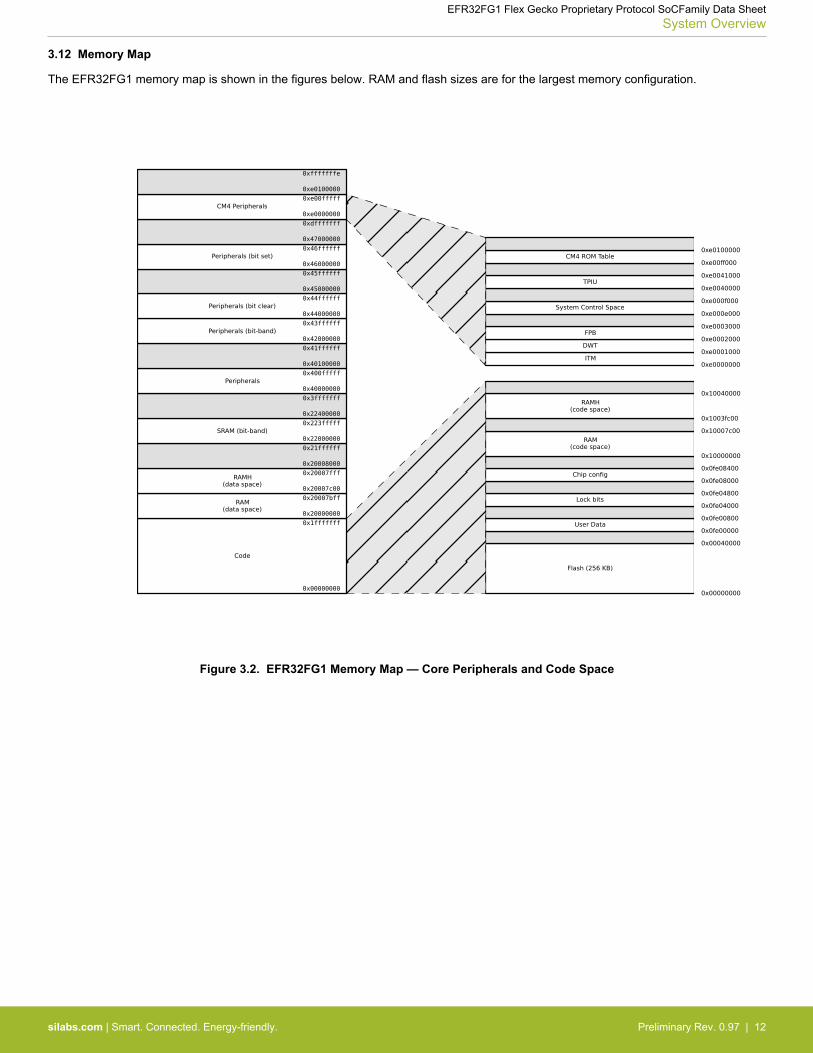
3.12 Memory Map
The EFR32FG1 memory map is shown in the figures below. RAM and flash sizes are for the largest memory configuration.
Figure 3.2. EFR32FG1 Memory Map — Core Peripherals and Code Space
EFR32FG1 Flex Gecko Proprietary Protocol SoCFamily Data SheetSystem Overview
silabs.com | Smart. Connected. Energy-friendly. Preliminary Rev. 0.97 | 12
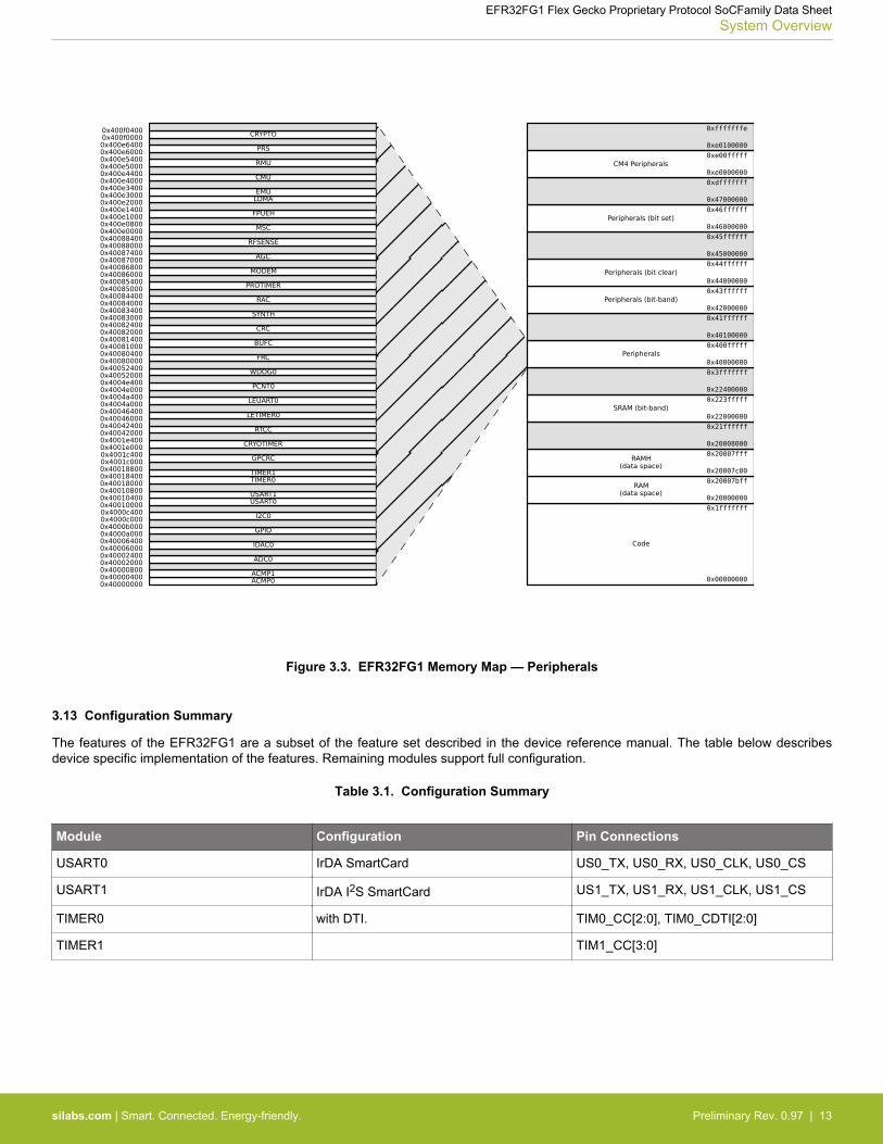
Figure 3.3. EFR32FG1 Memory Map — Peripherals
3.13 Configuration Summary
The features of the EFR32FG1 are a subset of the feature set described in the device reference manual. The table below describesdevice specific implementation of the features. Remaining modules support full configuration.
Table 3.1. Configuration Summary
Module Configuration Pin Connections
USART0 IrDA SmartCard US0_TX, US0_RX, US0_CLK, US0_CS
USART1 IrDA I2S SmartCard US1_TX, US1_RX, US1_CLK, US1_CS
TIMER0 with DTI. TIM0_CC[2:0], TIM0_CDTI[2:0]
TIMER1 TIM1_CC[3:0]
EFR32FG1 Flex Gecko Proprietary Protocol SoCFamily Data SheetSystem Overview
silabs.com | Smart. Connected. Energy-friendly. Preliminary Rev. 0.97 | 13
4. Electrical Specifications
4.1 Electrical Characteristics
All electrical parameters in all tables are specified under the following conditions, unless stated otherwise:• Typical values are based on TAMB=25 °C and VDD= 3.3 V, by production test and/or technology characterization.• Radio performance numbers are measured in conducted mode, based on Silicon Laboratories reference designs using output pow-
er-specific external RF impedance-matching networks for interfacing to a 50 Ω antenna.• Minimum and maximum values represent the worst conditions across supply voltage, process variation, and an operating tempera-
ture of -40 to +85 °C, unless stated otherwise.
Refer to Table 4.2 General Operating Conditions on page 17 for more details about operational supply and temperature limits.
EFR32FG1 Flex Gecko Proprietary Protocol SoCFamily Data SheetElectrical Specifications
silabs.com | Smart. Connected. Energy-friendly. Preliminary Rev. 0.97 | 14
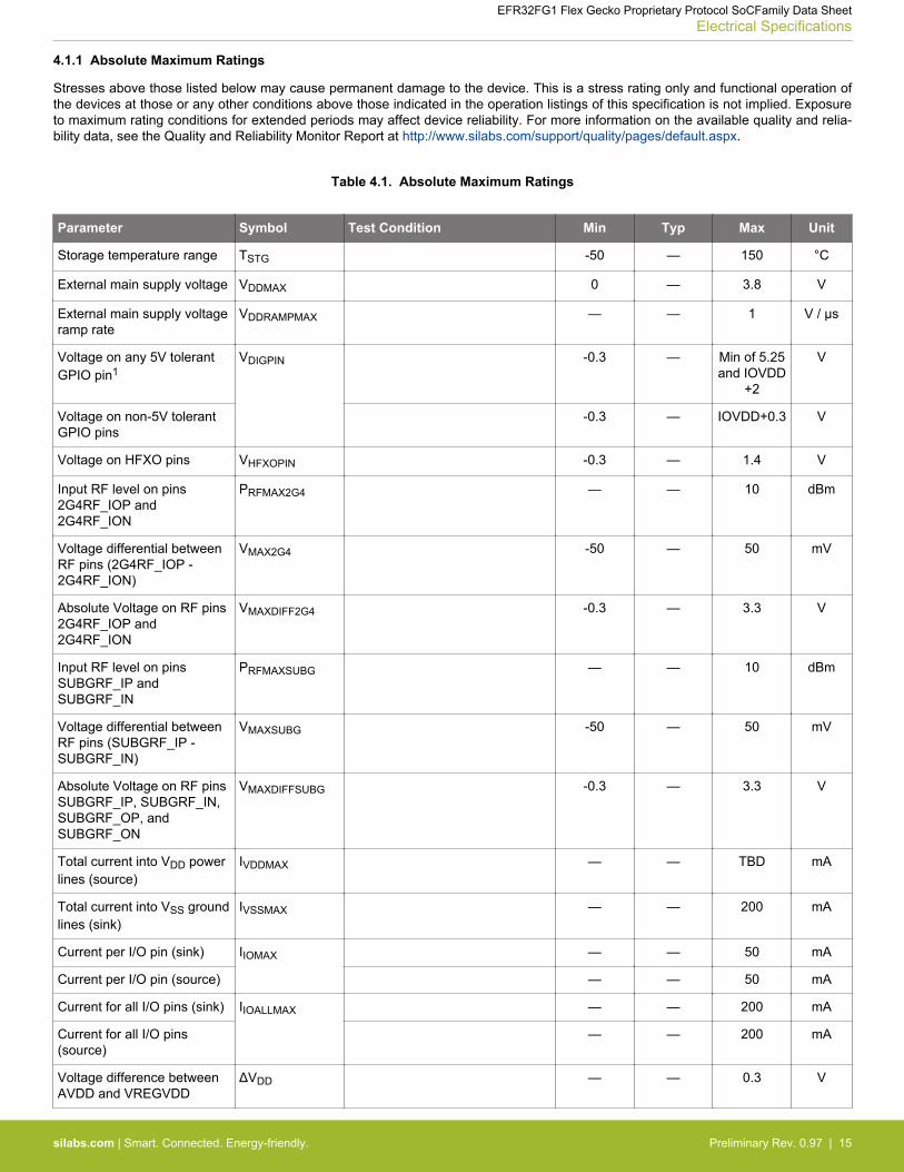
4.1.1 Absolute Maximum Ratings
Stresses above those listed below may cause permanent damage to the device. This is a stress rating only and functional operation ofthe devices at those or any other conditions above those indicated in the operation listings of this specification is not implied. Exposureto maximum rating conditions for extended periods may affect device reliability. For more information on the available quality and relia-bility data, see the Quality and Reliability Monitor Report at http://www.silabs.com/support/quality/pages/default.aspx.
Table 4.1. Absolute Maximum Ratings
Parameter Symbol Test Condition Min Typ Max Unit
Storage temperature range TSTG -50 — 150 °C
External main supply voltage VDDMAX 0 — 3.8 V
External main supply voltageramp rate
VDDRAMPMAX — — 1 V / μs
Voltage on any 5V tolerantGPIO pin1
VDIGPIN -0.3 — Min of 5.25and IOVDD
+2
V
Voltage on non-5V tolerantGPIO pins
-0.3 — IOVDD+0.3 V
Voltage on HFXO pins VHFXOPIN -0.3 — 1.4 V
Input RF level on pins2G4RF_IOP and2G4RF_ION
PRFMAX2G4 — — 10 dBm
Voltage differential betweenRF pins (2G4RF_IOP -2G4RF_ION)
VMAX2G4 -50 — 50 mV
Absolute Voltage on RF pins2G4RF_IOP and2G4RF_ION
VMAXDIFF2G4 -0.3 — 3.3 V
Input RF level on pinsSUBGRF_IP andSUBGRF_IN
PRFMAXSUBG — — 10 dBm
Voltage differential betweenRF pins (SUBGRF_IP -SUBGRF_IN)
VMAXSUBG -50 — 50 mV
Absolute Voltage on RF pinsSUBGRF_IP, SUBGRF_IN,SUBGRF_OP, andSUBGRF_ON
VMAXDIFFSUBG -0.3 — 3.3 V
Total current into VDD powerlines (source)
IVDDMAX — — TBD mA
Total current into VSS groundlines (sink)
IVSSMAX — — 200 mA
Current per I/O pin (sink) IIOMAX — — 50 mA
Current per I/O pin (source) — — 50 mA
Current for all I/O pins (sink) IIOALLMAX — — 200 mA
Current for all I/O pins(source)
— — 200 mA
Voltage difference betweenAVDD and VREGVDD
ΔVDD — — 0.3 V
EFR32FG1 Flex Gecko Proprietary Protocol SoCFamily Data SheetElectrical Specifications
silabs.com | Smart. Connected. Energy-friendly. Preliminary Rev. 0.97 | 15
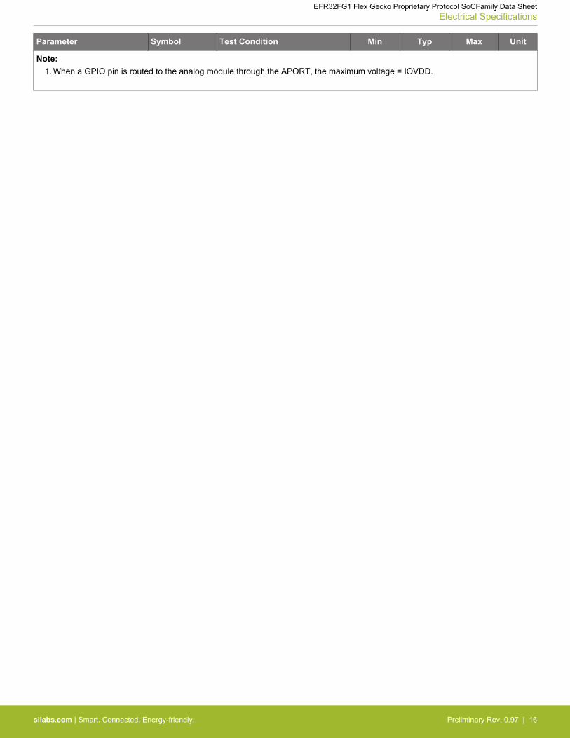
Parameter Symbol Test Condition Min Typ Max Unit
Note:1. When a GPIO pin is routed to the analog module through the APORT, the maximum voltage = IOVDD.
EFR32FG1 Flex Gecko Proprietary Protocol SoCFamily Data SheetElectrical Specifications
silabs.com | Smart. Connected. Energy-friendly. Preliminary Rev. 0.97 | 16
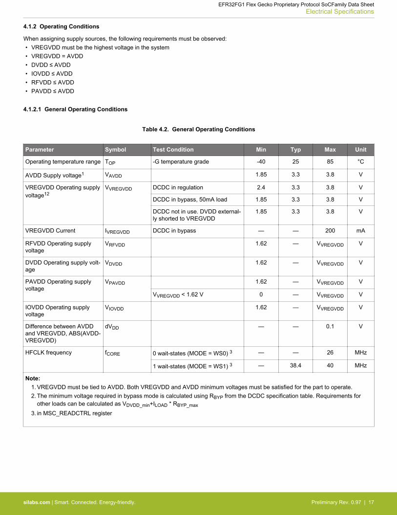
4.1.2 Operating Conditions
When assigning supply sources, the following requirements must be observed:• VREGVDD must be the highest voltage in the system• VREGVDD = AVDD• DVDD ≤ AVDD• IOVDD ≤ AVDD• RFVDD ≤ AVDD• PAVDD ≤ AVDD
4.1.2.1 General Operating Conditions
Table 4.2. General Operating Conditions
Parameter Symbol Test Condition Min Typ Max Unit
Operating temperature range TOP -G temperature grade -40 25 85 °C
AVDD Supply voltage1 VAVDD 1.85 3.3 3.8 V
VREGVDD Operating supplyvoltage12
VVREGVDD DCDC in regulation 2.4 3.3 3.8 V
DCDC in bypass, 50mA load 1.85 3.3 3.8 V
DCDC not in use. DVDD external-ly shorted to VREGVDD
1.85 3.3 3.8 V
VREGVDD Current IVREGVDD DCDC in bypass — — 200 mA
RFVDD Operating supplyvoltage
VRFVDD 1.62 — VVREGVDD V
DVDD Operating supply volt-age
VDVDD 1.62 — VVREGVDD V
PAVDD Operating supplyvoltage
VPAVDD 1.62 — VVREGVDD V
VVREGVDD < 1.62 V 0 — VVREGVDD V
IOVDD Operating supplyvoltage
VIOVDD 1.62 — VVREGVDD V
Difference between AVDDand VREGVDD, ABS(AVDD-VREGVDD)
dVDD — — 0.1 V
HFCLK frequency fCORE 0 wait-states (MODE = WS0) 3 — — 26 MHz
1 wait-states (MODE = WS1) 3 — 38.4 40 MHz
Note:1. VREGVDD must be tied to AVDD. Both VREGVDD and AVDD minimum voltages must be satisfied for the part to operate.2. The minimum voltage required in bypass mode is calculated using RBYP from the DCDC specification table. Requirements for
other loads can be calculated as VDVDD_min+ILOAD * RBYP_max
3. in MSC_READCTRL register
EFR32FG1 Flex Gecko Proprietary Protocol SoCFamily Data SheetElectrical Specifications
silabs.com | Smart. Connected. Energy-friendly. Preliminary Rev. 0.97 | 17
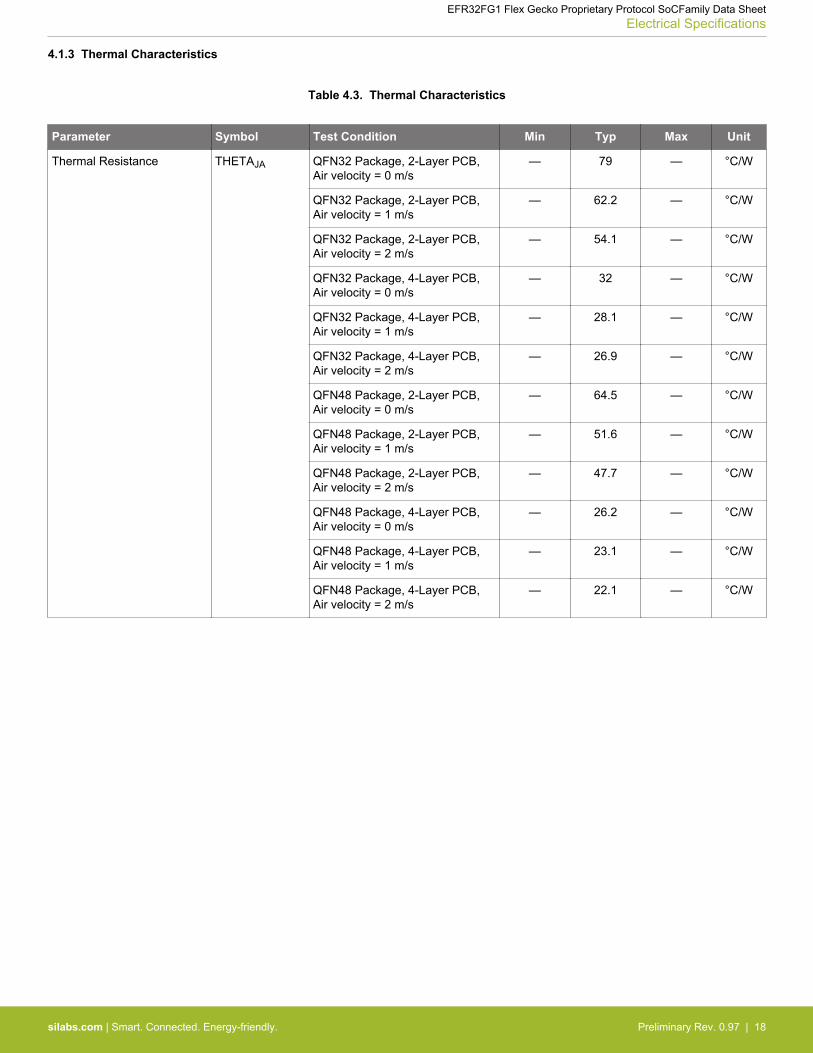
4.1.3 Thermal Characteristics
Table 4.3. Thermal Characteristics
Parameter Symbol Test Condition Min Typ Max Unit
Thermal Resistance THETAJA QFN32 Package, 2-Layer PCB,Air velocity = 0 m/s
— 79 — °C/W
QFN32 Package, 2-Layer PCB,Air velocity = 1 m/s
— 62.2 — °C/W
QFN32 Package, 2-Layer PCB,Air velocity = 2 m/s
— 54.1 — °C/W
QFN32 Package, 4-Layer PCB,Air velocity = 0 m/s
— 32 — °C/W
QFN32 Package, 4-Layer PCB,Air velocity = 1 m/s
— 28.1 — °C/W
QFN32 Package, 4-Layer PCB,Air velocity = 2 m/s
— 26.9 — °C/W
QFN48 Package, 2-Layer PCB,Air velocity = 0 m/s
— 64.5 — °C/W
QFN48 Package, 2-Layer PCB,Air velocity = 1 m/s
— 51.6 — °C/W
QFN48 Package, 2-Layer PCB,Air velocity = 2 m/s
— 47.7 — °C/W
QFN48 Package, 4-Layer PCB,Air velocity = 0 m/s
— 26.2 — °C/W
QFN48 Package, 4-Layer PCB,Air velocity = 1 m/s
— 23.1 — °C/W
QFN48 Package, 4-Layer PCB,Air velocity = 2 m/s
— 22.1 — °C/W
EFR32FG1 Flex Gecko Proprietary Protocol SoCFamily Data SheetElectrical Specifications
silabs.com | Smart. Connected. Energy-friendly. Preliminary Rev. 0.97 | 18
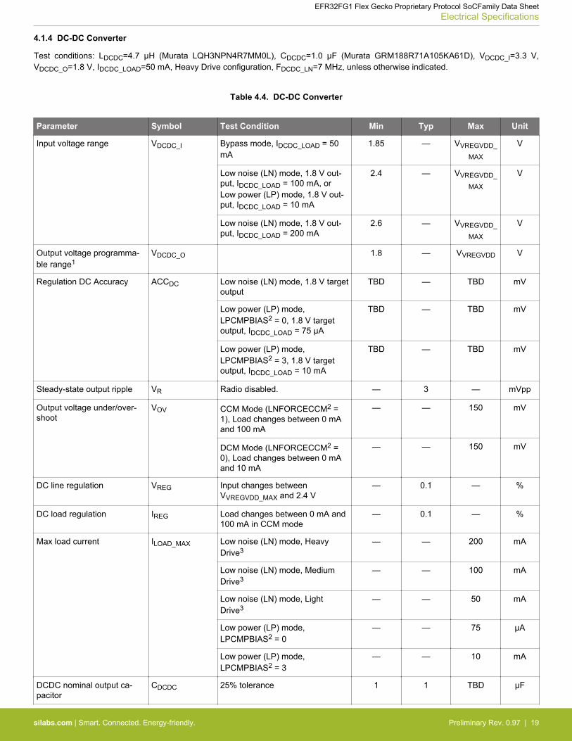
4.1.4 DC-DC Converter
Test conditions: LDCDC=4.7 µH (Murata LQH3NPN4R7MM0L), CDCDC=1.0 µF (Murata GRM188R71A105KA61D), VDCDC_I=3.3 V,VDCDC_O=1.8 V, IDCDC_LOAD=50 mA, Heavy Drive configuration, FDCDC_LN=7 MHz, unless otherwise indicated.
Table 4.4. DC-DC Converter
Parameter Symbol Test Condition Min Typ Max Unit
Input voltage range VDCDC_I Bypass mode, IDCDC_LOAD = 50mA
1.85 — VVREGVDD_
MAX
V
Low noise (LN) mode, 1.8 V out-put, IDCDC_LOAD = 100 mA, orLow power (LP) mode, 1.8 V out-put, IDCDC_LOAD = 10 mA
2.4 — VVREGVDD_
MAX
V
Low noise (LN) mode, 1.8 V out-put, IDCDC_LOAD = 200 mA
2.6 — VVREGVDD_
MAX
V
Output voltage programma-ble range1
VDCDC_O 1.8 — VVREGVDD V
Regulation DC Accuracy ACCDC Low noise (LN) mode, 1.8 V targetoutput
TBD — TBD mV
Low power (LP) mode,LPCMPBIAS2 = 0, 1.8 V targetoutput, IDCDC_LOAD = 75 μA
TBD — TBD mV
Low power (LP) mode,LPCMPBIAS2 = 3, 1.8 V targetoutput, IDCDC_LOAD = 10 mA
TBD — TBD mV
Steady-state output ripple VR Radio disabled. — 3 — mVpp
Output voltage under/over-shoot
VOV CCM Mode (LNFORCECCM2 =1), Load changes between 0 mAand 100 mA
— — 150 mV
DCM Mode (LNFORCECCM2 =0), Load changes between 0 mAand 10 mA
— — 150 mV
DC line regulation VREG Input changes betweenVVREGVDD_MAX and 2.4 V
— 0.1 — %
DC load regulation IREG Load changes between 0 mA and100 mA in CCM mode
— 0.1 — %
Max load current ILOAD_MAX Low noise (LN) mode, HeavyDrive3
— — 200 mA
Low noise (LN) mode, MediumDrive3
— — 100 mA
Low noise (LN) mode, LightDrive3
— — 50 mA
Low power (LP) mode,LPCMPBIAS2 = 0
— — 75 μA
Low power (LP) mode,LPCMPBIAS2 = 3
— — 10 mA
DCDC nominal output ca-pacitor
CDCDC 25% tolerance 1 1 TBD μF
EFR32FG1 Flex Gecko Proprietary Protocol SoCFamily Data SheetElectrical Specifications
silabs.com | Smart. Connected. Energy-friendly. Preliminary Rev. 0.97 | 19
Parameter Symbol Test Condition Min Typ Max Unit
DCDC nominal output induc-tor
LDCDC 20% tolerance 4.7 4.7 4.7 μH
Resistance in Bypass mode RBYP — 1.2 2.5 Ω
Note:1. Due to internal dropout, the DC-DC output will never be able to reach its input voltage, VVREGVDD
2. In EMU_DCDCMISCCTRL register3. Drive levels are defined by configuration of the PFETCNT and NFETCNT registers. Light Drive: PFETCNT=NFETCNT=3; Medi-
um Drive: PFETCNT=NFETCNT=7; Heavy Drive: PFETCNT=NFETCNT=15.
EFR32FG1 Flex Gecko Proprietary Protocol SoCFamily Data SheetElectrical Specifications
silabs.com | Smart. Connected. Energy-friendly. Preliminary Rev. 0.97 | 20
4.1.5 Current Consumption
4.1.5.1 Current Consumption 3.3 V without DC-DC Converter
Unless otherwise indicated, typical conditions are: VREGVDD = AVDD = DVDD = RFVDD = PAVDD= 3.3 V. TOP = 25 °C.EMU_PWRCFG_PWRCG=NODCDC. EMU_DCDCCTRL_DCDCMODE=BYPASS. Minimum and maximum values in this table repre-sent the worst conditions across supply voltage and process variation at TOP = 25 °C. See Figure 5.1 EFR32FG1 Typical ApplicationCircuit: Direct Supply Configuration without DC-DC converter on page 92.
Table 4.5. Current Consumption 3.3V without DC/DC
Parameter Symbol Test Condition Min Typ Max Unit
Current consumption in EM0Active mode with all periph-erals disabled
IACTIVE 38.4 MHz crystal, CPU runningwhile loop from flash1
— 130 — μA/MHz
38 MHz HFRCO, CPU runningPrime from flash
— 88 — μA/MHz
38 MHz HFRCO, CPU runningwhile loop from flash
— 100 105 μA/MHz
38 MHz HFRCO, CPU runningCoreMark from flash
— 112 — μA/MHz
26 MHz HFRCO, CPU runningwhile loop from flash
— 102 106 μA/MHz
1 MHz HFRCO, CPU runningwhile loop from flash
— 222 350 μA/MHz
Current consumption in EM1Sleep mode with all peripher-als disabled
IEM1 38.4 MHz crystal1 — 65 — μA/MHz
38 MHz HFRCO — 35 38 μA/MHz
26 MHz HFRCO — 37 41 μA/MHz
1 MHz HFRCO — 157 275 μA/MHz
Current consumption in EM2Deep Sleep mode.
IEM2 Full RAM retention and RTCCrunning from LFXO
— 3.3 — μA
4 kB RAM retention and RTCCrunning from LFRCO
— 3 6.3 μA
Current consumption in EM3Stop mode
IEM3 Full RAM retention and CRYO-TIMER running from ULFRCO
— 2.8 6 μA
Current consumption inEM4H Hibernate mode
IEM4 128 byte RAM retention, RTCCrunning from LFXO
— 1.1 — μA
128 byte RAM retention, CRYO-TIMER running from ULFRCO
— 0.65 — μA
128 byte RAM retention, no RTCC — 0.65 1.3 μA
Current consumption inEM4S Shutoff mode
IEM4S no RAM retention, no RTCC — 0.04 0.11 μA
Note:1. CMU_HFXOCTRL_LOWPOWER=0
EFR32FG1 Flex Gecko Proprietary Protocol SoCFamily Data SheetElectrical Specifications
silabs.com | Smart. Connected. Energy-friendly. Preliminary Rev. 0.97 | 21
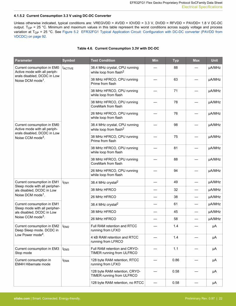
4.1.5.2 Current Consumption 3.3 V using DC-DC Converter
Unless otherwise indicated, typical conditions are: VREGVDD = AVDD = IOVDD = 3.3 V, DVDD = RFVDD = PAVDD= 1.8 V DC-DCoutput. TOP = 25 °C. Minimum and maximum values in this table represent the worst conditions across supply voltage and processvariation at TOP = 25 °C. See Figure 5.2 EFR32FG1 Typical Application Circuit: Configuration with DC-DC converter (PAVDD fromVDCDC) on page 92.
Table 4.6. Current Consumption 3.3V with DC-DC
Parameter Symbol Test Condition Min Typ Max Unit
Current consumption in EM0Active mode with all periph-erals disabled, DCDC in LowNoise DCM mode1.
IACTIVE 38.4 MHz crystal, CPU runningwhile loop from flash2
— 88 — μA/MHz
38 MHz HFRCO, CPU runningPrime from flash
— 63 — μA/MHz
38 MHz HFRCO, CPU runningwhile loop from flash
— 71 — μA/MHz
38 MHz HFRCO, CPU runningCoreMark from flash
— 78 — μA/MHz
26 MHz HFRCO, CPU runningwhile loop from flash
— 76 — μA/MHz
Current consumption in EM0Active mode with all periph-erals disabled, DCDC in LowNoise CCM mode3.
38.4 MHz crystal, CPU runningwhile loop from flash2
— 98 — μA/MHz
38 MHz HFRCO, CPU runningPrime from flash
— 75 — μA/MHz
38 MHz HFRCO, CPU runningwhile loop from flash
— 81 — μA/MHz
38 MHz HFRCO, CPU runningCoreMark from flash
— 88 — μA/MHz
26 MHz HFRCO, CPU runningwhile loop from flash
— 94 — μA/MHz
Current consumption in EM1Sleep mode with all peripher-als disabled, DCDC in LowNoise DCM mode1.
IEM1 38.4 MHz crystal2 — 49 — μA/MHz
38 MHz HFRCO — 32 — μA/MHz
26 MHz HFRCO — 38 — μA/MHz
Current consumption in EM1Sleep mode with all peripher-als disabled, DCDC in LowNoise CCM mode3.
38.4 MHz crystal2 — 61 — μA/MHz
38 MHz HFRCO — 45 — μA/MHz
26 MHz HFRCO — 58 — μA/MHz
Current consumption in EM2Deep Sleep mode. DCDC inLow Power mode4.
IEM2 Full RAM retention and RTCCrunning from LFXO
— 1.4 — μA
4 kB RAM retention and RTCCrunning from LFRCO
— 1.4 — μA
Current consumption in EM3Stop mode
IEM3 Full RAM retention and CRYO-TIMER running from ULFRCO
— 1.1 — μA
Current consumption inEM4H Hibernate mode
IEM4 128 byte RAM retention, RTCCrunning from LFXO
— 0.86 — μA
128 byte RAM retention, CRYO-TIMER running from ULFRCO
— 0.58 — μA
128 byte RAM retention, no RTCC — 0.58 — μA
EFR32FG1 Flex Gecko Proprietary Protocol SoCFamily Data SheetElectrical Specifications
silabs.com | Smart. Connected. Energy-friendly. Preliminary Rev. 0.97 | 22
Parameter Symbol Test Condition Min Typ Max Unit
Current consumption inEM4S Shutoff mode
IEM4S no RAM retention, no RTCC — 0.04 — μA
Note:1. DCDC Low Noise DCM Mode = Light Drive (PFETCNT=NFETCNT=3), F=3.0 MHz (RCOBAND=0), ANASW=DVDD2. CMU_HFXOCTRL_LOWPOWER=03. DCDC Low Noise CCM Mode = Light Drive (PFETCNT=NFETCNT=3), F=6.4 MHz (RCOBAND=4), ANASW=DVDD4. DCDC Low Power Mode = Medium Drive (PFETCNT=NFETCNT=7), LPOSCDIV=1, LPBIAS=3, LPCILIMSEL=1, ANASW=DVDD
EFR32FG1 Flex Gecko Proprietary Protocol SoCFamily Data SheetElectrical Specifications
silabs.com | Smart. Connected. Energy-friendly. Preliminary Rev. 0.97 | 23
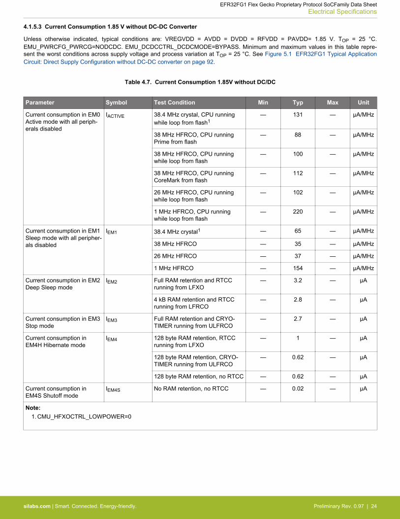
4.1.5.3 Current Consumption 1.85 V without DC-DC Converter
Unless otherwise indicated, typical conditions are: VREGVDD = AVDD = DVDD = RFVDD = PAVDD= 1.85 V. TOP = 25 °C.EMU_PWRCFG_PWRCG=NODCDC. EMU_DCDCCTRL_DCDCMODE=BYPASS. Minimum and maximum values in this table repre-sent the worst conditions across supply voltage and process variation at TOP = 25 °C. See Figure 5.1 EFR32FG1 Typical ApplicationCircuit: Direct Supply Configuration without DC-DC converter on page 92.
Table 4.7. Current Consumption 1.85V without DC/DC
Parameter Symbol Test Condition Min Typ Max Unit
Current consumption in EM0Active mode with all periph-erals disabled
IACTIVE 38.4 MHz crystal, CPU runningwhile loop from flash1
— 131 — μA/MHz
38 MHz HFRCO, CPU runningPrime from flash
— 88 — μA/MHz
38 MHz HFRCO, CPU runningwhile loop from flash
— 100 — μA/MHz
38 MHz HFRCO, CPU runningCoreMark from flash
— 112 — μA/MHz
26 MHz HFRCO, CPU runningwhile loop from flash
— 102 — μA/MHz
1 MHz HFRCO, CPU runningwhile loop from flash
— 220 — μA/MHz
Current consumption in EM1Sleep mode with all peripher-als disabled
IEM1 38.4 MHz crystal1 — 65 — μA/MHz
38 MHz HFRCO — 35 — μA/MHz
26 MHz HFRCO — 37 — μA/MHz
1 MHz HFRCO — 154 — μA/MHz
Current consumption in EM2Deep Sleep mode
IEM2 Full RAM retention and RTCCrunning from LFXO
— 3.2 — μA
4 kB RAM retention and RTCCrunning from LFRCO
— 2.8 — μA
Current consumption in EM3Stop mode
IEM3 Full RAM retention and CRYO-TIMER running from ULFRCO
— 2.7 — μA
Current consumption inEM4H Hibernate mode
IEM4 128 byte RAM retention, RTCCrunning from LFXO
— 1 — μA
128 byte RAM retention, CRYO-TIMER running from ULFRCO
— 0.62 — μA
128 byte RAM retention, no RTCC — 0.62 — μA
Current consumption inEM4S Shutoff mode
IEM4S No RAM retention, no RTCC — 0.02 — μA
Note:1. CMU_HFXOCTRL_LOWPOWER=0
EFR32FG1 Flex Gecko Proprietary Protocol SoCFamily Data SheetElectrical Specifications
silabs.com | Smart. Connected. Energy-friendly. Preliminary Rev. 0.97 | 24
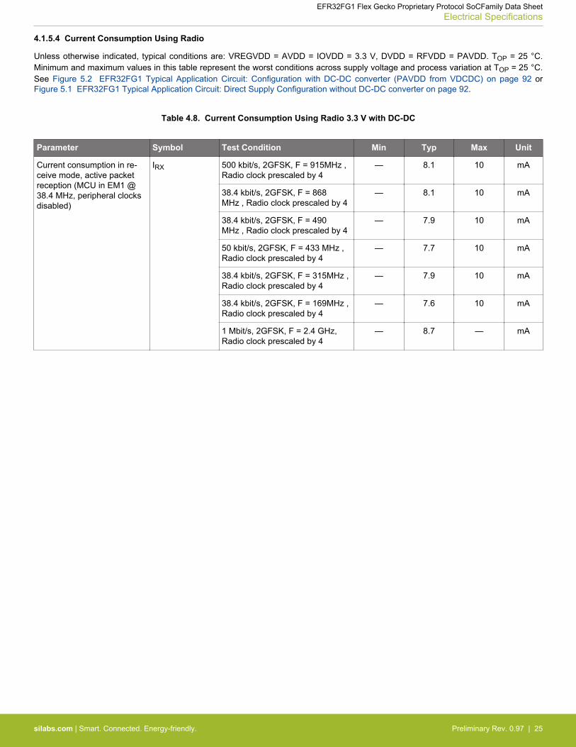
4.1.5.4 Current Consumption Using Radio
Unless otherwise indicated, typical conditions are: VREGVDD = AVDD = IOVDD = 3.3 V, DVDD = RFVDD = PAVDD. TOP = 25 °C.Minimum and maximum values in this table represent the worst conditions across supply voltage and process variation at TOP = 25 °C.See Figure 5.2 EFR32FG1 Typical Application Circuit: Configuration with DC-DC converter (PAVDD from VDCDC) on page 92 orFigure 5.1 EFR32FG1 Typical Application Circuit: Direct Supply Configuration without DC-DC converter on page 92.
Table 4.8. Current Consumption Using Radio 3.3 V with DC-DC
Parameter Symbol Test Condition Min Typ Max Unit
Current consumption in re-ceive mode, active packetreception (MCU in EM1 @38.4 MHz, peripheral clocksdisabled)
IRX 500 kbit/s, 2GFSK, F = 915MHz ,Radio clock prescaled by 4
— 8.1 10 mA
38.4 kbit/s, 2GFSK, F = 868MHz , Radio clock prescaled by 4
— 8.1 10 mA
38.4 kbit/s, 2GFSK, F = 490MHz , Radio clock prescaled by 4
— 7.9 10 mA
50 kbit/s, 2GFSK, F = 433 MHz ,Radio clock prescaled by 4
— 7.7 10 mA
38.4 kbit/s, 2GFSK, F = 315MHz ,Radio clock prescaled by 4
— 7.9 10 mA
38.4 kbit/s, 2GFSK, F = 169MHz ,Radio clock prescaled by 4
— 7.6 10 mA
1 Mbit/s, 2GFSK, F = 2.4 GHz,Radio clock prescaled by 4
— 8.7 — mA
EFR32FG1 Flex Gecko Proprietary Protocol SoCFamily Data SheetElectrical Specifications
silabs.com | Smart. Connected. Energy-friendly. Preliminary Rev. 0.97 | 25
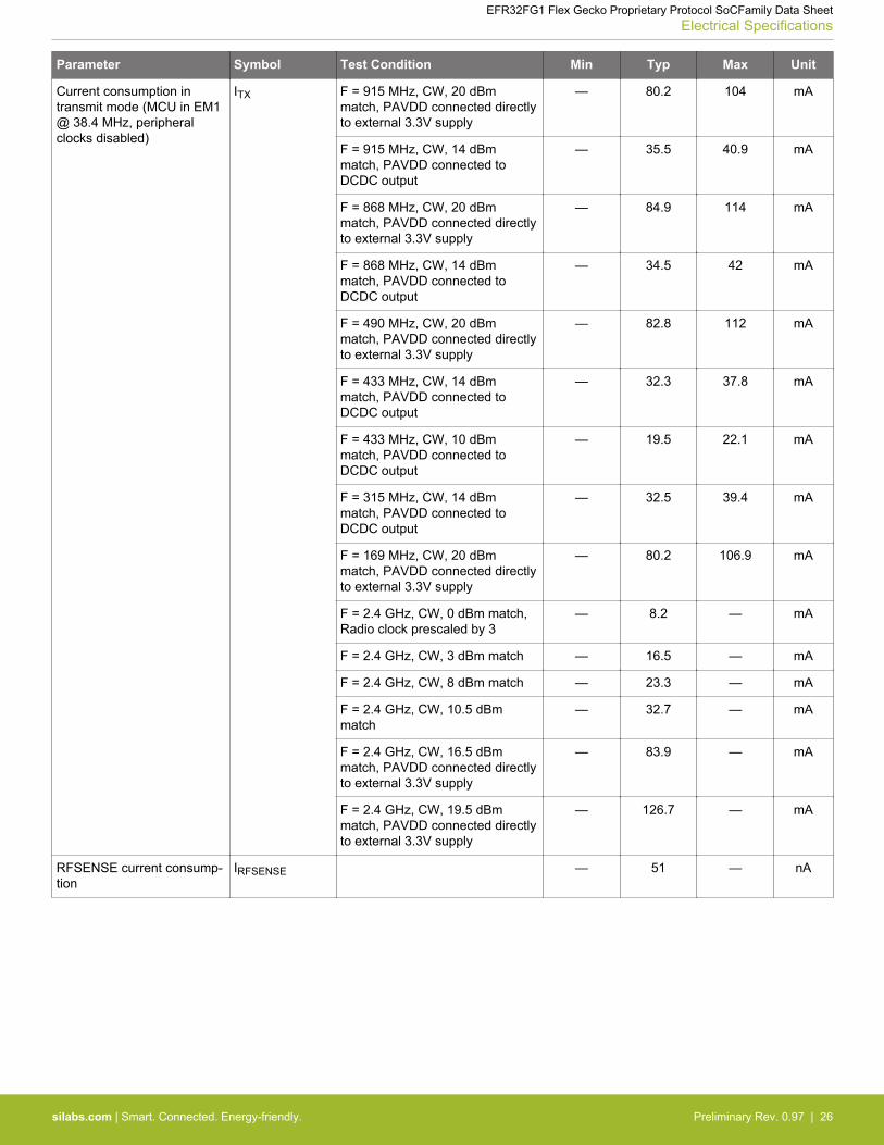
Parameter Symbol Test Condition Min Typ Max Unit
Current consumption intransmit mode (MCU in EM1@ 38.4 MHz, peripheralclocks disabled)
ITX F = 915 MHz, CW, 20 dBmmatch, PAVDD connected directlyto external 3.3V supply
— 80.2 104 mA
F = 915 MHz, CW, 14 dBmmatch, PAVDD connected toDCDC output
— 35.5 40.9 mA
F = 868 MHz, CW, 20 dBmmatch, PAVDD connected directlyto external 3.3V supply
— 84.9 114 mA
F = 868 MHz, CW, 14 dBmmatch, PAVDD connected toDCDC output
— 34.5 42 mA
F = 490 MHz, CW, 20 dBmmatch, PAVDD connected directlyto external 3.3V supply
— 82.8 112 mA
F = 433 MHz, CW, 14 dBmmatch, PAVDD connected toDCDC output
— 32.3 37.8 mA
F = 433 MHz, CW, 10 dBmmatch, PAVDD connected toDCDC output
— 19.5 22.1 mA
F = 315 MHz, CW, 14 dBmmatch, PAVDD connected toDCDC output
— 32.5 39.4 mA
F = 169 MHz, CW, 20 dBmmatch, PAVDD connected directlyto external 3.3V supply
— 80.2 106.9 mA
F = 2.4 GHz, CW, 0 dBm match,Radio clock prescaled by 3
— 8.2 — mA
F = 2.4 GHz, CW, 3 dBm match — 16.5 — mA
F = 2.4 GHz, CW, 8 dBm match — 23.3 — mA
F = 2.4 GHz, CW, 10.5 dBmmatch
— 32.7 — mA
F = 2.4 GHz, CW, 16.5 dBmmatch, PAVDD connected directlyto external 3.3V supply
— 83.9 — mA
F = 2.4 GHz, CW, 19.5 dBmmatch, PAVDD connected directlyto external 3.3V supply
— 126.7 — mA
RFSENSE current consump-tion
IRFSENSE — 51 — nA
EFR32FG1 Flex Gecko Proprietary Protocol SoCFamily Data SheetElectrical Specifications
silabs.com | Smart. Connected. Energy-friendly. Preliminary Rev. 0.97 | 26
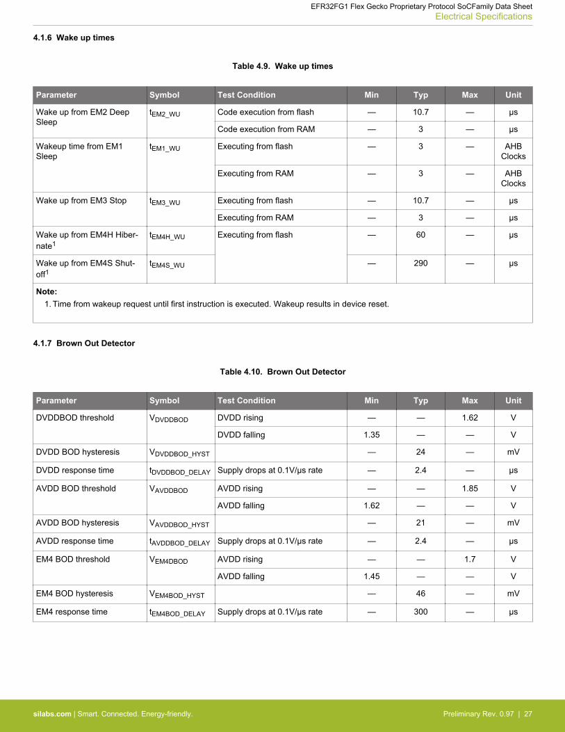
4.1.6 Wake up times
Table 4.9. Wake up times
Parameter Symbol Test Condition Min Typ Max Unit
Wake up from EM2 DeepSleep
tEM2_WU Code execution from flash — 10.7 — μs
Code execution from RAM — 3 — μs
Wakeup time from EM1Sleep
tEM1_WU Executing from flash — 3 — AHBClocks
Executing from RAM — 3 — AHBClocks
Wake up from EM3 Stop tEM3_WU Executing from flash — 10.7 — μs
Executing from RAM — 3 — μs
Wake up from EM4H Hiber-nate1
tEM4H_WU Executing from flash — 60 — μs
Wake up from EM4S Shut-off1
tEM4S_WU — 290 — μs
Note:1. Time from wakeup request until first instruction is executed. Wakeup results in device reset.
4.1.7 Brown Out Detector
Table 4.10. Brown Out Detector
Parameter Symbol Test Condition Min Typ Max Unit
DVDDBOD threshold VDVDDBOD DVDD rising — — 1.62 V
DVDD falling 1.35 — — V
DVDD BOD hysteresis VDVDDBOD_HYST — 24 — mV
DVDD response time tDVDDBOD_DELAY Supply drops at 0.1V/μs rate — 2.4 — μs
AVDD BOD threshold VAVDDBOD AVDD rising — — 1.85 V
AVDD falling 1.62 — — V
AVDD BOD hysteresis VAVDDBOD_HYST — 21 — mV
AVDD response time tAVDDBOD_DELAY Supply drops at 0.1V/μs rate — 2.4 — μs
EM4 BOD threshold VEM4DBOD AVDD rising — — 1.7 V
AVDD falling 1.45 — — V
EM4 BOD hysteresis VEM4BOD_HYST — 46 — mV
EM4 response time tEM4BOD_DELAY Supply drops at 0.1V/μs rate — 300 — μs
EFR32FG1 Flex Gecko Proprietary Protocol SoCFamily Data SheetElectrical Specifications
silabs.com | Smart. Connected. Energy-friendly. Preliminary Rev. 0.97 | 27
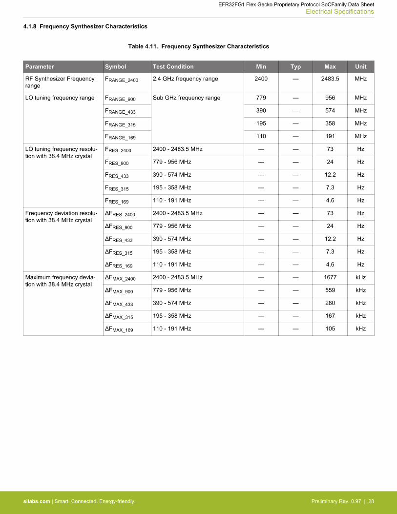
4.1.8 Frequency Synthesizer Characteristics
Table 4.11. Frequency Synthesizer Characteristics
Parameter Symbol Test Condition Min Typ Max Unit
RF Synthesizer Frequencyrange
FRANGE_2400 2.4 GHz frequency range 2400 — 2483.5 MHz
LO tuning frequency range FRANGE_900 Sub GHz frequency range 779 — 956 MHz
FRANGE_433 390 — 574 MHz
FRANGE_315 195 — 358 MHz
FRANGE_169 110 — 191 MHz
LO tuning frequency resolu-tion with 38.4 MHz crystal
FRES_2400 2400 - 2483.5 MHz — — 73 Hz
FRES_900 779 - 956 MHz — — 24 Hz
FRES_433 390 - 574 MHz — — 12.2 Hz
FRES_315 195 - 358 MHz — — 7.3 Hz
FRES_169 110 - 191 MHz — — 4.6 Hz
Frequency deviation resolu-tion with 38.4 MHz crystal
ΔFRES_2400 2400 - 2483.5 MHz — — 73 Hz
ΔFRES_900 779 - 956 MHz — — 24 Hz
ΔFRES_433 390 - 574 MHz — — 12.2 Hz
ΔFRES_315 195 - 358 MHz — — 7.3 Hz
ΔFRES_169 110 - 191 MHz — — 4.6 Hz
Maximum frequency devia-tion with 38.4 MHz crystal
ΔFMAX_2400 2400 - 2483.5 MHz — — 1677 kHz
ΔFMAX_900 779 - 956 MHz — — 559 kHz
ΔFMAX_433 390 - 574 MHz — — 280 kHz
ΔFMAX_315 195 - 358 MHz — — 167 kHz
ΔFMAX_169 110 - 191 MHz — — 105 kHz
EFR32FG1 Flex Gecko Proprietary Protocol SoCFamily Data SheetElectrical Specifications
silabs.com | Smart. Connected. Energy-friendly. Preliminary Rev. 0.97 | 28
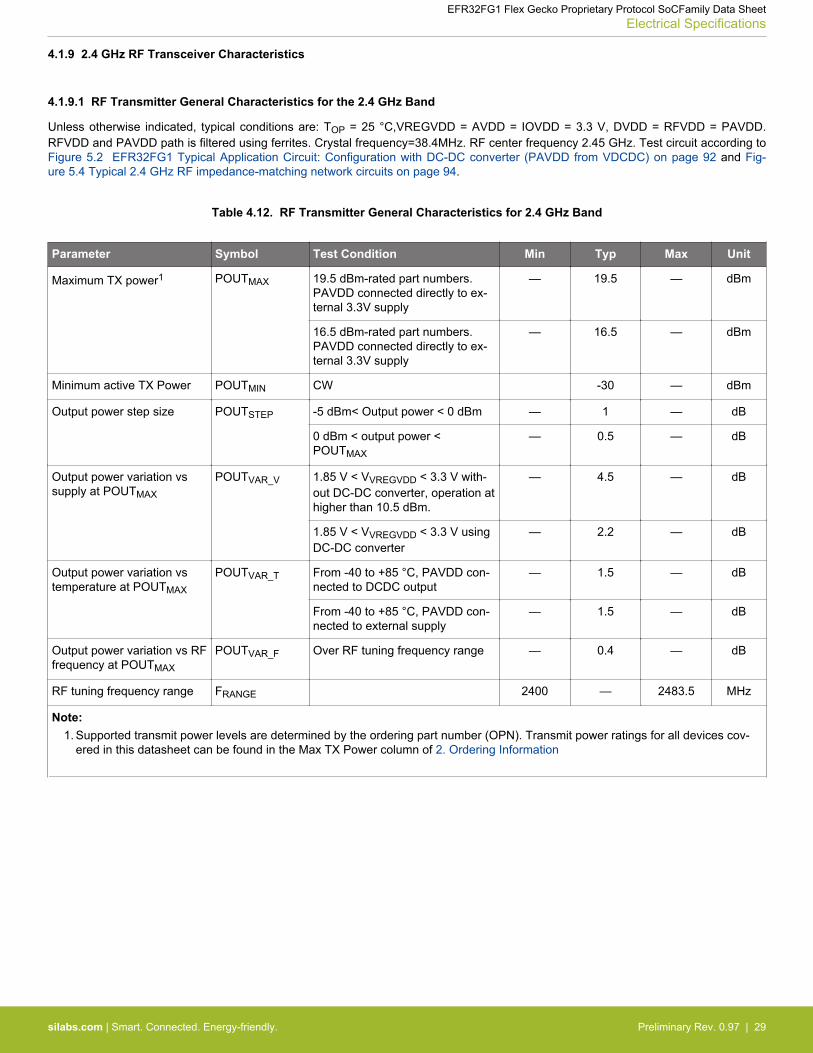
4.1.9 2.4 GHz RF Transceiver Characteristics
4.1.9.1 RF Transmitter General Characteristics for the 2.4 GHz Band
Unless otherwise indicated, typical conditions are: TOP = 25 °C,VREGVDD = AVDD = IOVDD = 3.3 V, DVDD = RFVDD = PAVDD.RFVDD and PAVDD path is filtered using ferrites. Crystal frequency=38.4MHz. RF center frequency 2.45 GHz. Test circuit according toFigure 5.2 EFR32FG1 Typical Application Circuit: Configuration with DC-DC converter (PAVDD from VDCDC) on page 92 and Fig-ure 5.4 Typical 2.4 GHz RF impedance-matching network circuits on page 94.
Table 4.12. RF Transmitter General Characteristics for 2.4 GHz Band
Parameter Symbol Test Condition Min Typ Max Unit
Maximum TX power1 POUTMAX 19.5 dBm-rated part numbers.PAVDD connected directly to ex-ternal 3.3V supply
— 19.5 — dBm
16.5 dBm-rated part numbers.PAVDD connected directly to ex-ternal 3.3V supply
— 16.5 — dBm
Minimum active TX Power POUTMIN CW -30 — dBm
Output power step size POUTSTEP -5 dBm< Output power < 0 dBm — 1 — dB
0 dBm < output power <POUTMAX
— 0.5 — dB
Output power variation vssupply at POUTMAX
POUTVAR_V 1.85 V < VVREGVDD < 3.3 V with-out DC-DC converter, operation athigher than 10.5 dBm.
— 4.5 — dB
1.85 V < VVREGVDD < 3.3 V usingDC-DC converter
— 2.2 — dB
Output power variation vstemperature at POUTMAX
POUTVAR_T From -40 to +85 °C, PAVDD con-nected to DCDC output
— 1.5 — dB
From -40 to +85 °C, PAVDD con-nected to external supply
— 1.5 — dB
Output power variation vs RFfrequency at POUTMAX
POUTVAR_F Over RF tuning frequency range — 0.4 — dB
RF tuning frequency range FRANGE 2400 — 2483.5 MHz
Note:1. Supported transmit power levels are determined by the ordering part number (OPN). Transmit power ratings for all devices cov-
ered in this datasheet can be found in the Max TX Power column of 2. Ordering Information
EFR32FG1 Flex Gecko Proprietary Protocol SoCFamily Data SheetElectrical Specifications
silabs.com | Smart. Connected. Energy-friendly. Preliminary Rev. 0.97 | 29
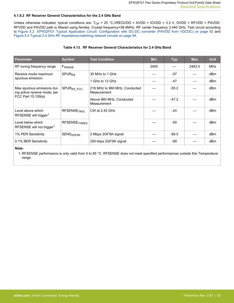
4.1.9.2 RF Receiver General Characteristics for the 2.4 GHz Band
Unless otherwise indicated, typical conditions are: TOP = 25 °C,VREGVDD = AVDD = IOVDD = 3.3 V, DVDD = RFVDD = PAVDD.RFVDD and PAVDD path is filtered using ferrites. Crystal frequency=38.4MHz. RF center frequency 2.440 GHz. Test circuit accordingto Figure 5.2 EFR32FG1 Typical Application Circuit: Configuration with DC-DC converter (PAVDD from VDCDC) on page 92 andFigure 5.4 Typical 2.4 GHz RF impedance-matching network circuits on page 94.
Table 4.13. RF Receiver General Characteristics for 2.4 GHz Band
Parameter Symbol Test Condition Min Typ Max Unit
RF tuning frequency range FRANGE 2400 — 2483.5 MHz
Receive mode maximumspurious emission
SPURRX 30 MHz to 1 GHz — -57 — dBm
1 GHz to 12 GHz — -47 — dBm
Max spurious emissions dur-ing active receive mode, perFCC Part 15.109(a)
SPURRX_FCC 216 MHz to 960 MHz, ConductedMeasurement
— -55.2 — dBm
Above 960 MHz, ConductedMeasurement
— -47.2 — dBm
Level above whichRFSENSE will trigger1
RFSENSETRIG CW at 2.45 GHz — -24 — dBm
Level below whichRFSENSE will not trigger1
RFSENSETHRES — -50 — dBm
1% PER Sensitivity SENS2GFSK 2 Mbps 2GFSK signal — -89.5 — dBm
0.1% BER Sensitivity 250 kbps 2GFSK signal — -99 — dBm
Note:1. RFSENSE performance is only valid from 0 to 85 °C. RFSENSE does not meet specified performances outside this Temperature
range.
EFR32FG1 Flex Gecko Proprietary Protocol SoCFamily Data SheetElectrical Specifications
silabs.com | Smart. Connected. Energy-friendly. Preliminary Rev. 0.97 | 30
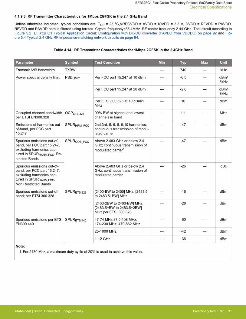
4.1.9.3 RF Transmitter Characteristics for 1Mbps 2GFSK in the 2.4 GHz Band
Unless otherwise indicated, typical conditions are: TOP = 25 °C,VREGVDD = AVDD = IOVDD = 3.3 V, DVDD = RFVDD = PAVDD.RFVDD and PAVDD path is filtered using ferrites. Crystal frequency=38.4MHz. RF center frequency 2.44 GHz. Test circuit according toFigure 5.2 EFR32FG1 Typical Application Circuit: Configuration with DC-DC converter (PAVDD from VDCDC) on page 92 and Fig-ure 5.4 Typical 2.4 GHz RF impedance-matching network circuits on page 94.
Table 4.14. RF Transmitter Characteristics for 1Mbps 2GFSK in the 2.4GHz Band
Parameter Symbol Test Condition Min Typ Max Unit
Transmit 6dB bandwidth TXBW — 740 — kHz
Power spectral density limit PSDLIMIT Per FCC part 15.247 at 10 dBm — -6.5 — dBm/3kHz
Per FCC part 15.247 at 20 dBm — -2.6 — dBm/3kHz
Per ETSI 300.328 at 10 dBm/1MHz
— 10 — dBm
Occupied channel bandwidthper ETSI EN300.328
OCPETSI328 99% BW at highest and lowestchannels in band
— 1.1 — MHz
Emissions of harmonics out-of-band, per FCC part15.247
SPURHRM_FCC 2nd,3rd, 5, 6, 8, 9,10 harmonics;continuous transmission of modu-lated carrier
— -47 — dBm
Spurious emissions out-of-band, per FCC part 15.247,excluding harmonics cap-tured in SPURHARM,FCC. Re-stricted Bands
SPUROOB_FCC Above 2.483 GHz or below 2.4GHz; continuous transmission ofmodulated carrier1
— -47 — dBm
Spurious emissions out-of-band, per FCC part 15.247,excluding harmonics cap-tured in SPURHARM,FCC.Non Restricted Bands
Above 2.483 GHz or below 2.4GHz; continuous transmission ofmodulated carrier
— -26 — dBc
Spurious emissions out-of-band; per ETSI 300.328
SPURETSI328 [2400-BW to 2400] MHz, [2483.5to 2483.5+BW] MHz
— -16 — dBm
[2400-2BW to 2400-BW] MHz,[2483.5+BW to 2483.5+2BW]MHz per ETSI 300.328
— -26 — dBm
Spurious emissions per ETSIEN300.440
SPURETSI440 47-74 MHz,87.5-108 MHz,174-230 MHz, 470-862 MHz
— -60 — dBm
25-1000 MHz — -42 — dBm
1-12 GHz — -36 — dBm
Note:1. For 2480 Mhz, a maximum duty cycle of 20% is used to achieve this value.
EFR32FG1 Flex Gecko Proprietary Protocol SoCFamily Data SheetElectrical Specifications
silabs.com | Smart. Connected. Energy-friendly. Preliminary Rev. 0.97 | 31
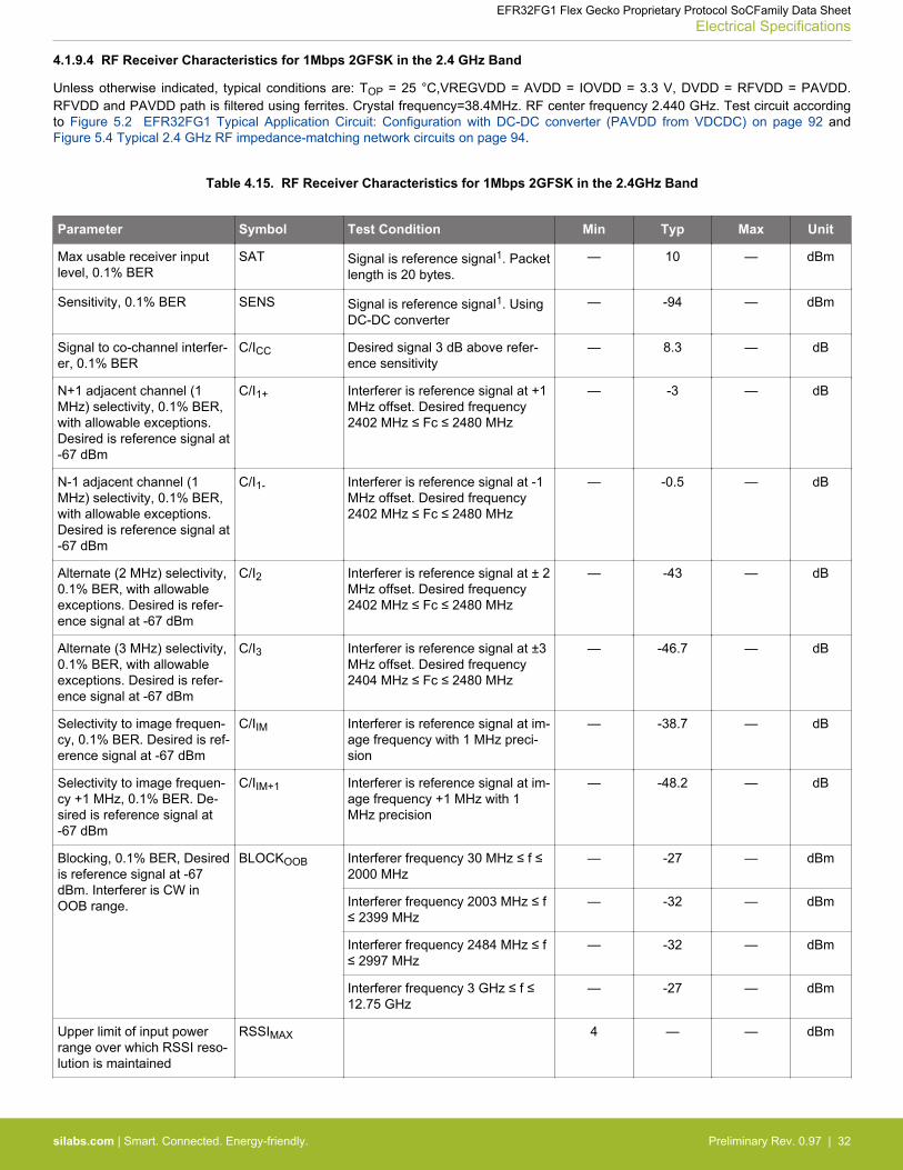
4.1.9.4 RF Receiver Characteristics for 1Mbps 2GFSK in the 2.4 GHz Band
Unless otherwise indicated, typical conditions are: TOP = 25 °C,VREGVDD = AVDD = IOVDD = 3.3 V, DVDD = RFVDD = PAVDD.RFVDD and PAVDD path is filtered using ferrites. Crystal frequency=38.4MHz. RF center frequency 2.440 GHz. Test circuit accordingto Figure 5.2 EFR32FG1 Typical Application Circuit: Configuration with DC-DC converter (PAVDD from VDCDC) on page 92 andFigure 5.4 Typical 2.4 GHz RF impedance-matching network circuits on page 94.
Table 4.15. RF Receiver Characteristics for 1Mbps 2GFSK in the 2.4GHz Band
Parameter Symbol Test Condition Min Typ Max Unit
Max usable receiver inputlevel, 0.1% BER
SAT Signal is reference signal1. Packetlength is 20 bytes.
— 10 — dBm
Sensitivity, 0.1% BER SENS Signal is reference signal1. UsingDC-DC converter
— -94 — dBm
Signal to co-channel interfer-er, 0.1% BER
C/ICC Desired signal 3 dB above refer-ence sensitivity
— 8.3 — dB
N+1 adjacent channel (1MHz) selectivity, 0.1% BER,with allowable exceptions.Desired is reference signal at-67 dBm
C/I1+ Interferer is reference signal at +1MHz offset. Desired frequency2402 MHz ≤ Fc ≤ 2480 MHz
— -3 — dB
N-1 adjacent channel (1MHz) selectivity, 0.1% BER,with allowable exceptions.Desired is reference signal at-67 dBm
C/I1- Interferer is reference signal at -1MHz offset. Desired frequency2402 MHz ≤ Fc ≤ 2480 MHz
— -0.5 — dB
Alternate (2 MHz) selectivity,0.1% BER, with allowableexceptions. Desired is refer-ence signal at -67 dBm
C/I2 Interferer is reference signal at ± 2MHz offset. Desired frequency2402 MHz ≤ Fc ≤ 2480 MHz
— -43 — dB
Alternate (3 MHz) selectivity,0.1% BER, with allowableexceptions. Desired is refer-ence signal at -67 dBm
C/I3 Interferer is reference signal at ±3MHz offset. Desired frequency2404 MHz ≤ Fc ≤ 2480 MHz
— -46.7 — dB
Selectivity to image frequen-cy, 0.1% BER. Desired is ref-erence signal at -67 dBm
C/IIM Interferer is reference signal at im-age frequency with 1 MHz preci-sion
— -38.7 — dB
Selectivity to image frequen-cy +1 MHz, 0.1% BER. De-sired is reference signal at-67 dBm
C/IIM+1 Interferer is reference signal at im-age frequency +1 MHz with 1MHz precision
— -48.2 — dB
Blocking, 0.1% BER, Desiredis reference signal at -67dBm. Interferer is CW inOOB range.
BLOCKOOB Interferer frequency 30 MHz ≤ f ≤2000 MHz
— -27 — dBm
Interferer frequency 2003 MHz ≤ f≤ 2399 MHz
— -32 — dBm
Interferer frequency 2484 MHz ≤ f≤ 2997 MHz
— -32 — dBm
Interferer frequency 3 GHz ≤ f ≤12.75 GHz
— -27 — dBm
Upper limit of input powerrange over which RSSI reso-lution is maintained
RSSIMAX 4 — — dBm
EFR32FG1 Flex Gecko Proprietary Protocol SoCFamily Data SheetElectrical Specifications
silabs.com | Smart. Connected. Energy-friendly. Preliminary Rev. 0.97 | 32
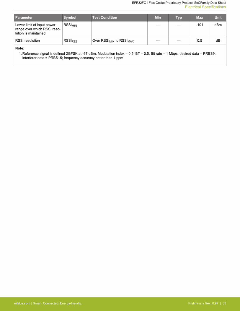
Parameter Symbol Test Condition Min Typ Max Unit
Lower limit of input powerrange over which RSSI reso-lution is maintained
RSSIMIN — — -101 dBm
RSSI resolution RSSIRES Over RSSIMIN to RSSIMAX — — 0.5 dB
Note:1. Reference signal is defined 2GFSK at -67 dBm, Modulation index = 0.5, BT = 0.5, Bit rate = 1 Mbps, desired data = PRBS9;
interferer data = PRBS15; frequency accuracy better than 1 ppm
EFR32FG1 Flex Gecko Proprietary Protocol SoCFamily Data SheetElectrical Specifications
silabs.com | Smart. Connected. Energy-friendly. Preliminary Rev. 0.97 | 33
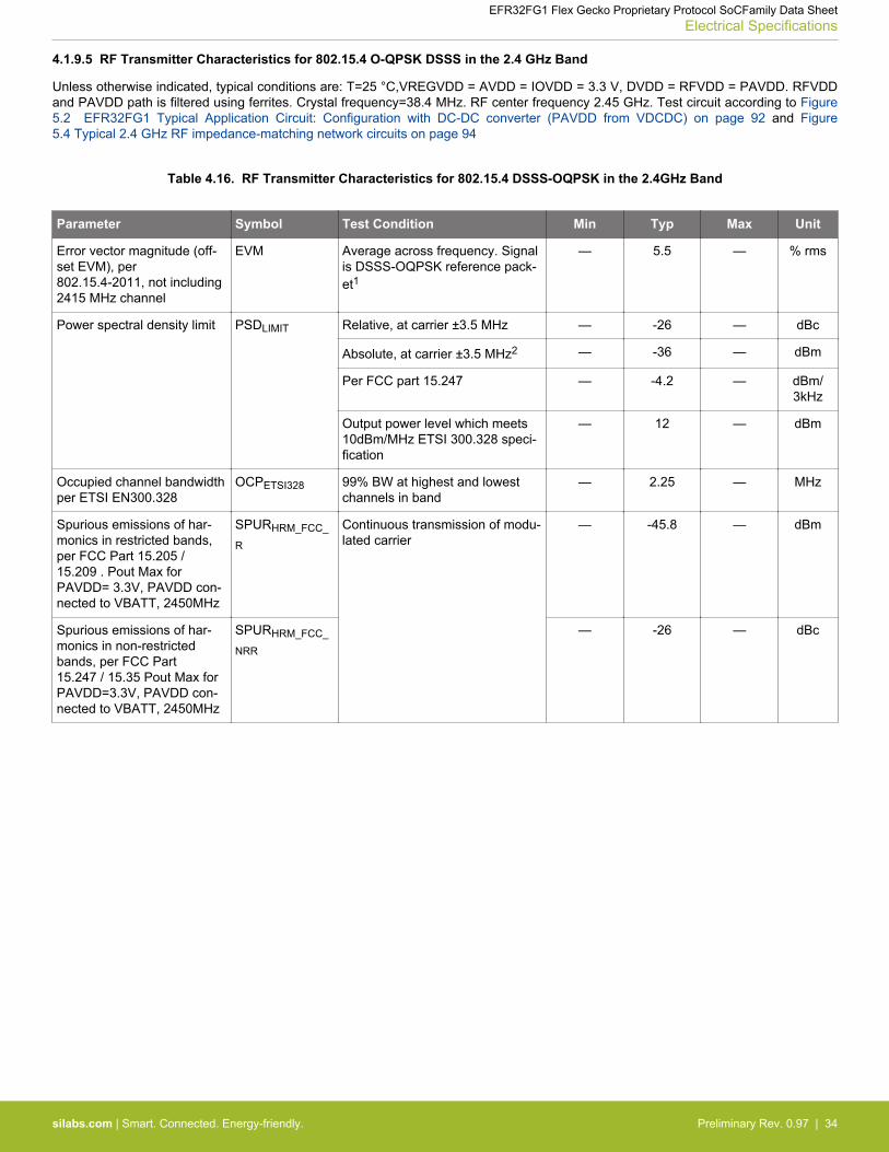
4.1.9.5 RF Transmitter Characteristics for 802.15.4 O-QPSK DSSS in the 2.4 GHz Band
Unless otherwise indicated, typical conditions are: T=25 °C,VREGVDD = AVDD = IOVDD = 3.3 V, DVDD = RFVDD = PAVDD. RFVDDand PAVDD path is filtered using ferrites. Crystal frequency=38.4 MHz. RF center frequency 2.45 GHz. Test circuit according to Figure5.2 EFR32FG1 Typical Application Circuit: Configuration with DC-DC converter (PAVDD from VDCDC) on page 92 and Figure5.4 Typical 2.4 GHz RF impedance-matching network circuits on page 94
Table 4.16. RF Transmitter Characteristics for 802.15.4 DSSS-OQPSK in the 2.4GHz Band
Parameter Symbol Test Condition Min Typ Max Unit
Error vector magnitude (off-set EVM), per802.15.4-2011, not including2415 MHz channel
EVM Average across frequency. Signalis DSSS-OQPSK reference pack-et1
— 5.5 — % rms
Power spectral density limit PSDLIMIT Relative, at carrier ±3.5 MHz — -26 — dBc
Absolute, at carrier ±3.5 MHz2 — -36 — dBm
Per FCC part 15.247 — -4.2 — dBm/3kHz
Output power level which meets10dBm/MHz ETSI 300.328 speci-fication
— 12 — dBm
Occupied channel bandwidthper ETSI EN300.328
OCPETSI328 99% BW at highest and lowestchannels in band
— 2.25 — MHz
Spurious emissions of har-monics in restricted bands,per FCC Part 15.205 /15.209 . Pout Max forPAVDD= 3.3V, PAVDD con-nected to VBATT, 2450MHz
SPURHRM_FCC_
R
Continuous transmission of modu-lated carrier
— -45.8 — dBm
Spurious emissions of har-monics in non-restrictedbands, per FCC Part15.247 / 15.35 Pout Max forPAVDD=3.3V, PAVDD con-nected to VBATT, 2450MHz
SPURHRM_FCC_
NRR
— -26 — dBc
EFR32FG1 Flex Gecko Proprietary Protocol SoCFamily Data SheetElectrical Specifications
silabs.com | Smart. Connected. Energy-friendly. Preliminary Rev. 0.97 | 34
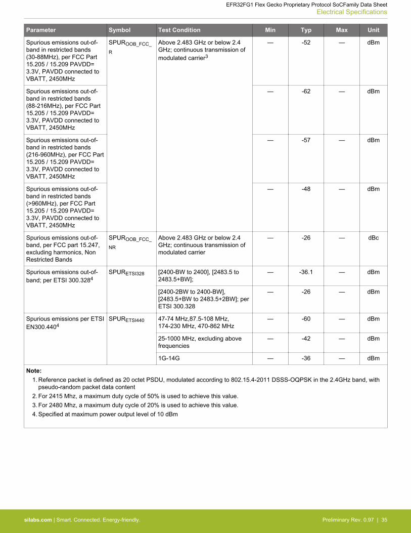
Parameter Symbol Test Condition Min Typ Max Unit
Spurious emissions out-of-band in restricted bands(30-88MHz), per FCC Part15.205 / 15.209 PAVDD=3.3V, PAVDD connected toVBATT, 2450MHz
SPUROOB_FCC_
R
Above 2.483 GHz or below 2.4GHz; continuous transmission ofmodulated carrier3
— -52 — dBm
Spurious emissions out-of-band in restricted bands(88-216MHz), per FCC Part15.205 / 15.209 PAVDD=3.3V, PAVDD connected toVBATT, 2450MHz
— -62 — dBm
Spurious emissions out-of-band in restricted bands(216-960MHz), per FCC Part15.205 / 15.209 PAVDD=3.3V, PAVDD connected toVBATT, 2450MHz
— -57 — dBm
Spurious emissions out-of-band in restricted bands(>960MHz), per FCC Part15.205 / 15.209 PAVDD=3.3V, PAVDD connected toVBATT, 2450MHz
— -48 — dBm
Spurious emissions out-of-band, per FCC part 15.247,excluding harmonics, NonRestricted Bands
SPUROOB_FCC_
NR
Above 2.483 GHz or below 2.4GHz; continuous transmission ofmodulated carrier
— -26 — dBc
Spurious emissions out-of-band; per ETSI 300.3284
SPURETSI328 [2400-BW to 2400], [2483.5 to2483.5+BW];
— -36.1 — dBm
[2400-2BW to 2400-BW],[2483.5+BW to 2483.5+2BW]; perETSI 300.328
— -26 — dBm
Spurious emissions per ETSIEN300.4404
SPURETSI440 47-74 MHz,87.5-108 MHz,174-230 MHz, 470-862 MHz
— -60 — dBm
25-1000 MHz, excluding abovefrequencies
— -42 — dBm
1G-14G — -36 — dBm
Note:1. Reference packet is defined as 20 octet PSDU, modulated according to 802.15.4-2011 DSSS-OQPSK in the 2.4GHz band, with
pseudo-random packet data content2. For 2415 Mhz, a maximum duty cycle of 50% is used to achieve this value.3. For 2480 Mhz, a maximum duty cycle of 20% is used to achieve this value.4. Specified at maximum power output level of 10 dBm
EFR32FG1 Flex Gecko Proprietary Protocol SoCFamily Data SheetElectrical Specifications
silabs.com | Smart. Connected. Energy-friendly. Preliminary Rev. 0.97 | 35
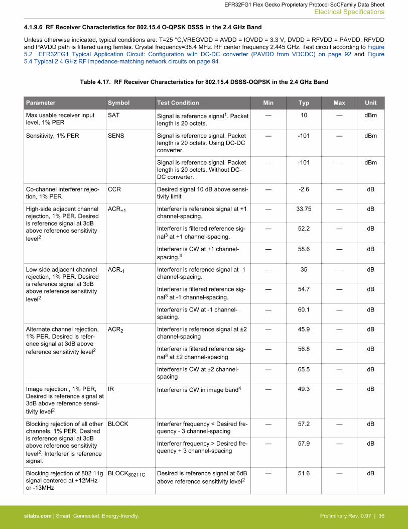
4.1.9.6 RF Receiver Characteristics for 802.15.4 O-QPSK DSSS in the 2.4 GHz Band
Unless otherwise indicated, typical conditions are: T=25 °C,VREGVDD = AVDD = IOVDD = 3.3 V, DVDD = RFVDD = PAVDD. RFVDDand PAVDD path is filtered using ferrites. Crystal frequency=38.4 MHz. RF center frequency 2.445 GHz. Test circuit according to Figure5.2 EFR32FG1 Typical Application Circuit: Configuration with DC-DC converter (PAVDD from VDCDC) on page 92 and Figure5.4 Typical 2.4 GHz RF impedance-matching network circuits on page 94
Table 4.17. RF Receiver Characteristics for 802.15.4 DSSS-OQPSK in the 2.4 GHz Band
Parameter Symbol Test Condition Min Typ Max Unit
Max usable receiver inputlevel, 1% PER
SAT Signal is reference signal1. Packetlength is 20 octets.
— 10 — dBm
Sensitivity, 1% PER SENS Signal is reference signal. Packetlength is 20 octets. Using DC-DCconverter.
— -101 — dBm
Signal is reference signal. Packetlength is 20 octets. Without DC-DC converter.
— -101 — dBm
Co-channel interferer rejec-tion, 1% PER
CCR Desired signal 10 dB above sensi-tivity limit
— -2.6 — dB
High-side adjacent channelrejection, 1% PER. Desiredis reference signal at 3dBabove reference sensitivitylevel2
ACR+1 Interferer is reference signal at +1channel-spacing.
— 33.75 — dB
Interferer is filtered reference sig-nal3 at +1 channel-spacing.
— 52.2 — dB
Interferer is CW at +1 channel-spacing.4
— 58.6 — dB
Low-side adjacent channelrejection, 1% PER. Desiredis reference signal at 3dBabove reference sensitivitylevel2
ACR-1 Interferer is reference signal at -1channel-spacing.
— 35 — dB
Interferer is filtered reference sig-nal3 at -1 channel-spacing.
— 54.7 — dB
Interferer is CW at -1 channel-spacing.
— 60.1 — dB
Alternate channel rejection,1% PER. Desired is refer-ence signal at 3dB abovereference sensitivity level2
ACR2 Interferer is reference signal at ±2channel-spacing
— 45.9 — dB
Interferer is filtered reference sig-nal3 at ±2 channel-spacing
— 56.8 — dB
Interferer is CW at ±2 channel-spacing
— 65.5 — dB
Image rejection , 1% PER,Desired is reference signal at3dB above reference sensi-tivity level2
IR Interferer is CW in image band4 — 49.3 — dB
Blocking rejection of all otherchannels. 1% PER, Desiredis reference signal at 3dBabove reference sensitivitylevel2. Interferer is referencesignal.
BLOCK Interferer frequency < Desired fre-quency - 3 channel-spacing
— 57.2 — dB
Interferer frequency > Desired fre-quency + 3 channel-spacing
— 57.9 — dB
Blocking rejection of 802.11gsignal centered at +12MHzor -13MHz
BLOCK80211G Desired is reference signal at 6dBabove reference sensitivity level2
— 51.6 — dB
EFR32FG1 Flex Gecko Proprietary Protocol SoCFamily Data SheetElectrical Specifications
silabs.com | Smart. Connected. Energy-friendly. Preliminary Rev. 0.97 | 36
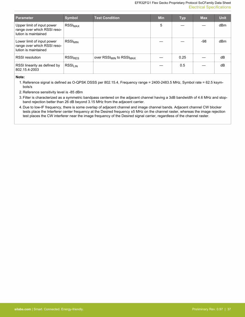
Parameter Symbol Test Condition Min Typ Max Unit
Upper limit of input powerrange over which RSSI reso-lution is maintained
RSSIMAX 5 — — dBm
Lower limit of input powerrange over which RSSI reso-lution is maintained
RSSIMIN — — -98 dBm
RSSI resolution RSSIRES over RSSIMIN to RSSIMAX — 0.25 — dB
RSSI linearity as defined by802.15.4-2003
RSSILIN — 0.5 — dB
Note:1. Reference signal is defined as O-QPSK DSSS per 802.15.4, Frequency range = 2400-2483.5 MHz, Symbol rate = 62.5 ksym-
bols/s2. Reference sensitivity level is -85 dBm3. Filter is characterized as a symmetric bandpass centered on the adjacent channel having a 3dB bandwidth of 4.6 MHz and stop-
band rejection better than 26 dB beyond 3.15 MHz from the adjacent carrier.4. Due to low-IF frequency, there is some overlap of adjacent channel and image channel bands. Adjacent channel CW blocker
tests place the Interferer center frequency at the Desired frequency ±5 MHz on the channel raster, whereas the image rejectiontest places the CW interferer near the image frequency of the Desired signal carrier, regardless of the channel raster.
EFR32FG1 Flex Gecko Proprietary Protocol SoCFamily Data SheetElectrical Specifications
silabs.com | Smart. Connected. Energy-friendly. Preliminary Rev. 0.97 | 37
4.1.10 Sub-GHz RF Transceiver Characteristics
EFR32FG1 Flex Gecko Proprietary Protocol SoCFamily Data SheetElectrical Specifications
silabs.com | Smart. Connected. Energy-friendly. Preliminary Rev. 0.97 | 38
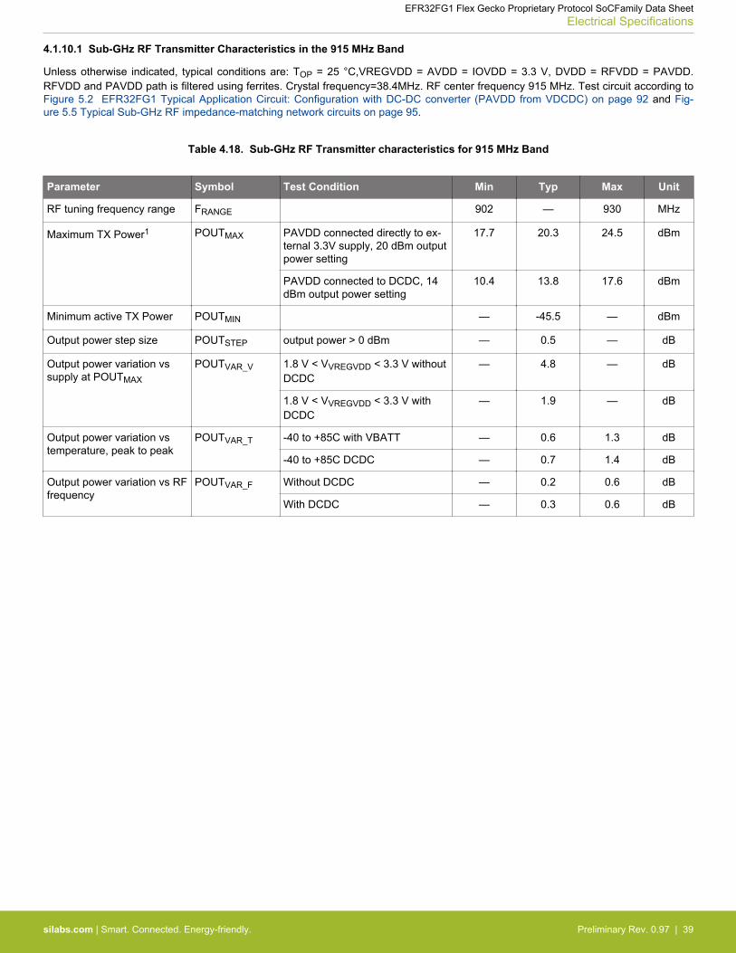
4.1.10.1 Sub-GHz RF Transmitter Characteristics in the 915 MHz Band
Unless otherwise indicated, typical conditions are: TOP = 25 °C,VREGVDD = AVDD = IOVDD = 3.3 V, DVDD = RFVDD = PAVDD.RFVDD and PAVDD path is filtered using ferrites. Crystal frequency=38.4MHz. RF center frequency 915 MHz. Test circuit according toFigure 5.2 EFR32FG1 Typical Application Circuit: Configuration with DC-DC converter (PAVDD from VDCDC) on page 92 and Fig-ure 5.5 Typical Sub-GHz RF impedance-matching network circuits on page 95.
Table 4.18. Sub-GHz RF Transmitter characteristics for 915 MHz Band
Parameter Symbol Test Condition Min Typ Max Unit
RF tuning frequency range FRANGE 902 — 930 MHz
Maximum TX Power1 POUTMAX PAVDD connected directly to ex-ternal 3.3V supply, 20 dBm outputpower setting
17.7 20.3 24.5 dBm
PAVDD connected to DCDC, 14dBm output power setting
10.4 13.8 17.6 dBm
Minimum active TX Power POUTMIN — -45.5 — dBm
Output power step size POUTSTEP output power > 0 dBm — 0.5 — dB
Output power variation vssupply at POUTMAX
POUTVAR_V 1.8 V < VVREGVDD < 3.3 V withoutDCDC
— 4.8 — dB
1.8 V < VVREGVDD < 3.3 V withDCDC
— 1.9 — dB
Output power variation vstemperature, peak to peak
POUTVAR_T -40 to +85C with VBATT — 0.6 1.3 dB
-40 to +85C DCDC — 0.7 1.4 dB
Output power variation vs RFfrequency
POUTVAR_F Without DCDC — 0.2 0.6 dB
With DCDC — 0.3 0.6 dB
EFR32FG1 Flex Gecko Proprietary Protocol SoCFamily Data SheetElectrical Specifications
silabs.com | Smart. Connected. Energy-friendly. Preliminary Rev. 0.97 | 39
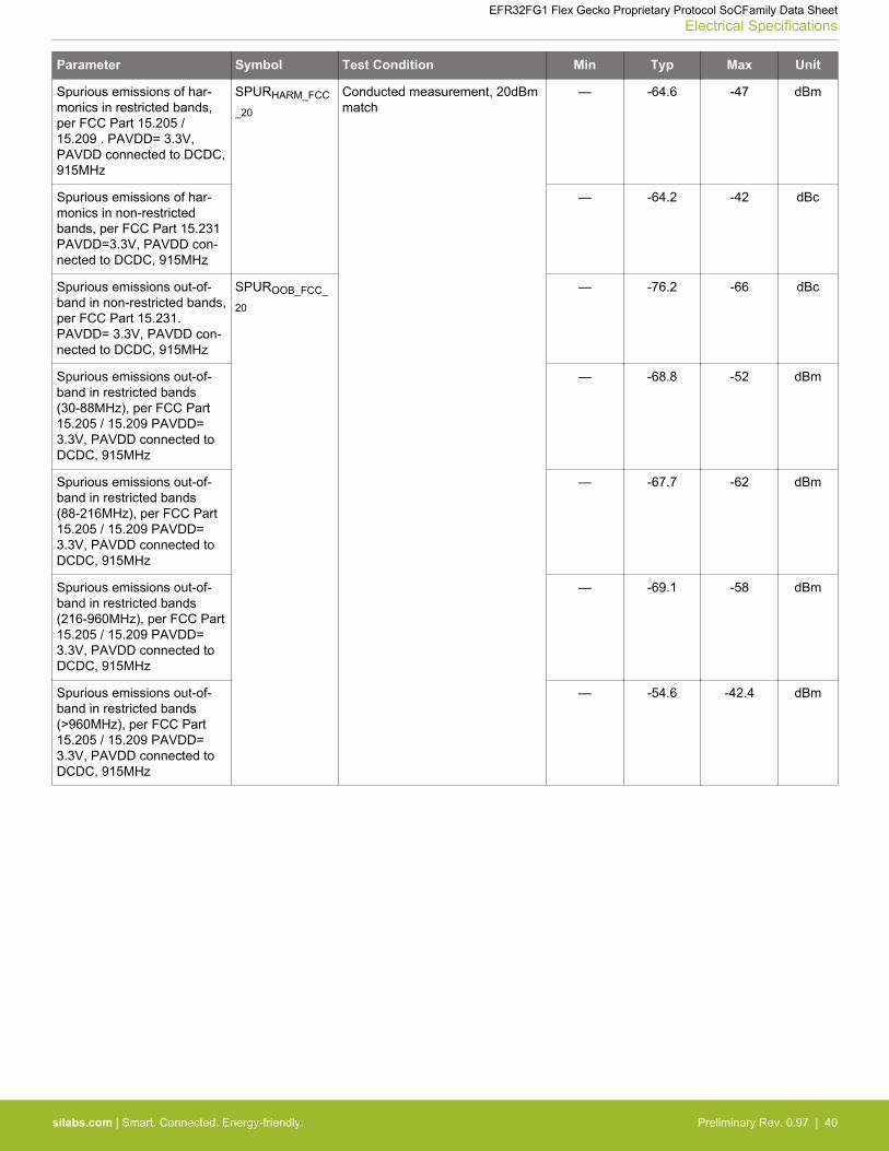
Parameter Symbol Test Condition Min Typ Max Unit
Spurious emissions of har-monics in restricted bands,per FCC Part 15.205 /15.209 . PAVDD= 3.3V,PAVDD connected to DCDC,915MHz
SPURHARM_FCC
_20
Conducted measurement, 20dBmmatch
— -64.6 -47 dBm
Spurious emissions of har-monics in non-restrictedbands, per FCC Part 15.231PAVDD=3.3V, PAVDD con-nected to DCDC, 915MHz
— -64.2 -42 dBc
Spurious emissions out-of-band in non-restricted bands,per FCC Part 15.231.PAVDD= 3.3V, PAVDD con-nected to DCDC, 915MHz
SPUROOB_FCC_
20
— -76.2 -66 dBc
Spurious emissions out-of-band in restricted bands(30-88MHz), per FCC Part15.205 / 15.209 PAVDD=3.3V, PAVDD connected toDCDC, 915MHz
— -68.8 -52 dBm
Spurious emissions out-of-band in restricted bands(88-216MHz), per FCC Part15.205 / 15.209 PAVDD=3.3V, PAVDD connected toDCDC, 915MHz
— -67.7 -62 dBm
Spurious emissions out-of-band in restricted bands(216-960MHz), per FCC Part15.205 / 15.209 PAVDD=3.3V, PAVDD connected toDCDC, 915MHz
— -69.1 -58 dBm
Spurious emissions out-of-band in restricted bands(>960MHz), per FCC Part15.205 / 15.209 PAVDD=3.3V, PAVDD connected toDCDC, 915MHz
— -54.6 -42.4 dBm
EFR32FG1 Flex Gecko Proprietary Protocol SoCFamily Data SheetElectrical Specifications
silabs.com | Smart. Connected. Energy-friendly. Preliminary Rev. 0.97 | 40
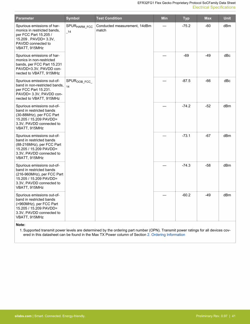
Parameter Symbol Test Condition Min Typ Max Unit
Spurious emissions of har-monics in restricted bands,per FCC Part 15.205 /15.209 . PAVDD= 3.3V,PAVDD connected toVBATT, 915MHz
SPURHARM_FCC
_14
Conducted measurement, 14dBmmatch
— -75.2 -60 dBm
Spurious emissions of har-monics in non-restrictedbands, per FCC Part 15.231PAVDD=3.3V, PAVDD con-nected to VBATT, 915MHz
— -69 -49 dBc
Spurious emissions out-of-band in non-restricted bands,per FCC Part 15.231.PAVDD= 3.3V, PAVDD con-nected to VBATT, 915MHz
SPUROOB_FCC_
14
— -87.5 -66 dBc
Spurious emissions out-of-band in restricted bands(30-88MHz), per FCC Part15.205 / 15.209 PAVDD=3.3V, PAVDD connected toVBATT, 915MHz
— -74.2 -52 dBm
Spurious emissions out-of-band in restricted bands(88-216MHz), per FCC Part15.205 / 15.209 PAVDD=3.3V, PAVDD connected toVBATT, 915MHz
— -73.1 -67 dBm
Spurious emissions out-of-band in restricted bands(216-960MHz), per FCC Part15.205 / 15.209 PAVDD=3.3V, PAVDD connected toVBATT, 915MHz
— -74.3 -58 dBm
Spurious emissions out-of-band in restricted bands(>960MHz), per FCC Part15.205 / 15.209 PAVDD=3.3V, PAVDD connected toVBATT, 915MHz
— -60.2 -49 dBm
Note:1. Supported transmit power levels are determined by the ordering part number (OPN). Transmit power ratings for all devices cov-
ered in this datasheet can be found in the Max TX Power column of Section 2. Ordering Information
EFR32FG1 Flex Gecko Proprietary Protocol SoCFamily Data SheetElectrical Specifications
silabs.com | Smart. Connected. Energy-friendly. Preliminary Rev. 0.97 | 41
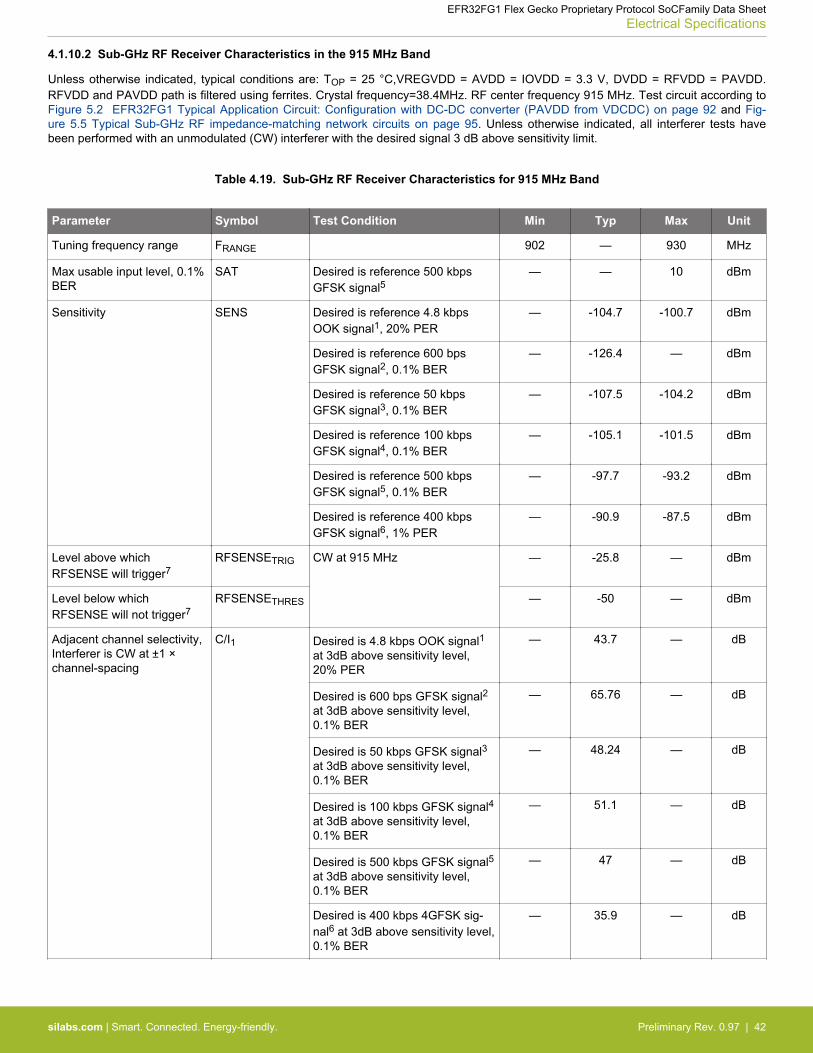
4.1.10.2 Sub-GHz RF Receiver Characteristics in the 915 MHz Band
Unless otherwise indicated, typical conditions are: TOP = 25 °C,VREGVDD = AVDD = IOVDD = 3.3 V, DVDD = RFVDD = PAVDD.RFVDD and PAVDD path is filtered using ferrites. Crystal frequency=38.4MHz. RF center frequency 915 MHz. Test circuit according toFigure 5.2 EFR32FG1 Typical Application Circuit: Configuration with DC-DC converter (PAVDD from VDCDC) on page 92 and Fig-ure 5.5 Typical Sub-GHz RF impedance-matching network circuits on page 95. Unless otherwise indicated, all interferer tests havebeen performed with an unmodulated (CW) interferer with the desired signal 3 dB above sensitivity limit.
Table 4.19. Sub-GHz RF Receiver Characteristics for 915 MHz Band
Parameter Symbol Test Condition Min Typ Max Unit
Tuning frequency range FRANGE 902 — 930 MHz
Max usable input level, 0.1%BER
SAT Desired is reference 500 kbpsGFSK signal5
— — 10 dBm
Sensitivity SENS Desired is reference 4.8 kbpsOOK signal1, 20% PER
— -104.7 -100.7 dBm
Desired is reference 600 bpsGFSK signal2, 0.1% BER
— -126.4 — dBm
Desired is reference 50 kbpsGFSK signal3, 0.1% BER
— -107.5 -104.2 dBm
Desired is reference 100 kbpsGFSK signal4, 0.1% BER
— -105.1 -101.5 dBm
Desired is reference 500 kbpsGFSK signal5, 0.1% BER
— -97.7 -93.2 dBm
Desired is reference 400 kbpsGFSK signal6, 1% PER
— -90.9 -87.5 dBm
Level above whichRFSENSE will trigger7
RFSENSETRIG CW at 915 MHz — -25.8 — dBm
Level below whichRFSENSE will not trigger7
RFSENSETHRES — -50 — dBm
Adjacent channel selectivity,Interferer is CW at ±1 ×channel-spacing
C/I1 Desired is 4.8 kbps OOK signal1at 3dB above sensitivity level,20% PER
— 43.7 — dB
Desired is 600 bps GFSK signal2at 3dB above sensitivity level,0.1% BER
— 65.76 — dB
Desired is 50 kbps GFSK signal3at 3dB above sensitivity level,0.1% BER
— 48.24 — dB
Desired is 100 kbps GFSK signal4at 3dB above sensitivity level,0.1% BER
— 51.1 — dB
Desired is 500 kbps GFSK signal5at 3dB above sensitivity level,0.1% BER
— 47 — dB
Desired is 400 kbps 4GFSK sig-nal6 at 3dB above sensitivity level,0.1% BER
— 35.9 — dB
EFR32FG1 Flex Gecko Proprietary Protocol SoCFamily Data SheetElectrical Specifications
silabs.com | Smart. Connected. Energy-friendly. Preliminary Rev. 0.97 | 42
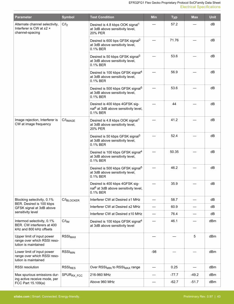
Parameter Symbol Test Condition Min Typ Max Unit
Alternate channel selectivity,Interferer is CW at ±2 ×channel-spacing
C/I2 Desired is 4.8 kbps OOK signal1at 3dB above sensitivity level,20% PER
— 57.2 — dB
Desired is 600 bps GFSK signal2at 3dB above sensitivity level,0.1% BER
— 71.76 — dB
Desired is 50 kbps GFSK signal3at 3dB above sensitivity level,0.1% BER
— 53.6 — dB
Desired is 100 kbps GFSK signal4at 3dB above sensitivity level,0.1% BER
— 56.9 — dB
Desired is 500 kbps GFSK signal5at 3dB above sensitivity level,0.1% BER
— 53.6 — dB
Desired is 400 kbps 4GFSK sig-nal6 at 3dB above sensitivity level,0.1% BER
— 44 — dB
Image rejection, Interferer isCW at image frequency
C/IIMAGE Desired is 4.8 kbps OOK signal1at 3dB above sensitivity level,20% PER
— 41.2 — dB
Desired is 50 kbps GFSK signal3at 3dB above sensitivity level,0.1% BER
— 52.4 — dB
Desired is 100 kbps GFSK signal4at 3dB above sensitivity level,0.1% BER
— 50.35 — dB
Desired is 500 kbps GFSK signal5at 3dB above sensitivity level,0.1% BER
— 46.2 — dB
Desired is 400 kbps 4GFSK sig-nal6 at 3dB above sensitivity level,0.1% BER
— 35.9 — dB
Blocking selectivity, 0.1%BER. Desired is 100 kbpsGFSK signal at 3dB abovesensitivity level
C/IBLOCKER Interferer CW at Desired ±1 MHz — 58.7 — dB
Interferer CW at Desired ±2 MHz — 60.9 — dB
Interferer CW at Desired ±10 MHz — 76.4 — dB
Intermod selectivity, 0.1%BER. CW interferers at 400kHz and 800 kHz offsets
C/IIM Desired is 100 kbps GFSK signal4at 3dB above sensitivity level
— 46.1 — dBm
Upper limit of input powerrange over which RSSI reso-lution is maintained
RSSIMAX — — 5 dBm
Lower limit of input powerrange over which RSSI reso-lution is maintained
RSSIMIN -98 — — dBm
RSSI resolution RSSIRES Over RSSIMIN to RSSIMAX range — 0.25 — dBm
Max spurious emissions dur-ing active receive mode, perFCC Part 15.109(a)
SPURRX_FCC 216-960 MHz — -77.7 -49.2 dBm
Above 960 MHz — -62.7 -51.7 dBm
EFR32FG1 Flex Gecko Proprietary Protocol SoCFamily Data SheetElectrical Specifications
silabs.com | Smart. Connected. Energy-friendly. Preliminary Rev. 0.97 | 43
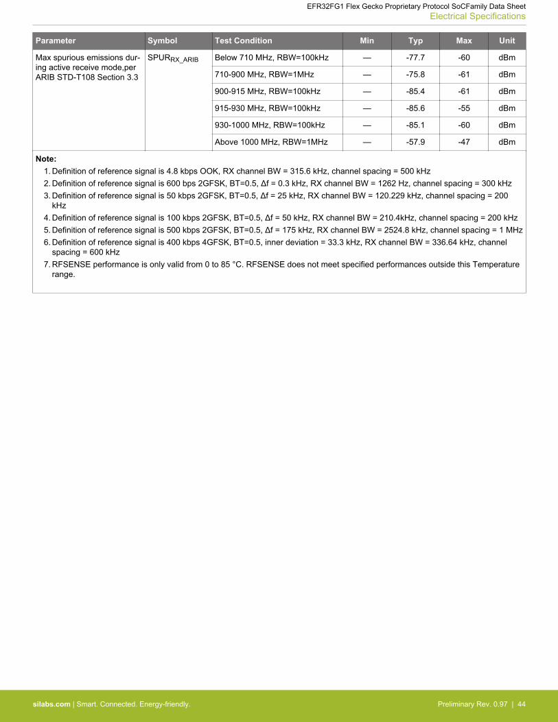
Parameter Symbol Test Condition Min Typ Max Unit
Max spurious emissions dur-ing active receive mode,perARIB STD-T108 Section 3.3
SPURRX_ARIB Below 710 MHz, RBW=100kHz — -77.7 -60 dBm
710-900 MHz, RBW=1MHz — -75.8 -61 dBm
900-915 MHz, RBW=100kHz — -85.4 -61 dBm
915-930 MHz, RBW=100kHz — -85.6 -55 dBm
930-1000 MHz, RBW=100kHz — -85.1 -60 dBm
Above 1000 MHz, RBW=1MHz — -57.9 -47 dBm
Note:1. Definition of reference signal is 4.8 kbps OOK, RX channel BW = 315.6 kHz, channel spacing = 500 kHz2. Definition of reference signal is 600 bps 2GFSK, BT=0.5, Δf = 0.3 kHz, RX channel BW = 1262 Hz, channel spacing = 300 kHz3. Definition of reference signal is 50 kbps 2GFSK, BT=0.5, Δf = 25 kHz, RX channel BW = 120.229 kHz, channel spacing = 200
kHz4. Definition of reference signal is 100 kbps 2GFSK, BT=0.5, Δf = 50 kHz, RX channel BW = 210.4kHz, channel spacing = 200 kHz5. Definition of reference signal is 500 kbps 2GFSK, BT=0.5, Δf = 175 kHz, RX channel BW = 2524.8 kHz, channel spacing = 1 MHz6. Definition of reference signal is 400 kbps 4GFSK, BT=0.5, inner deviation = 33.3 kHz, RX channel BW = 336.64 kHz, channel
spacing = 600 kHz7. RFSENSE performance is only valid from 0 to 85 °C. RFSENSE does not meet specified performances outside this Temperature
range.
EFR32FG1 Flex Gecko Proprietary Protocol SoCFamily Data SheetElectrical Specifications
silabs.com | Smart. Connected. Energy-friendly. Preliminary Rev. 0.97 | 44
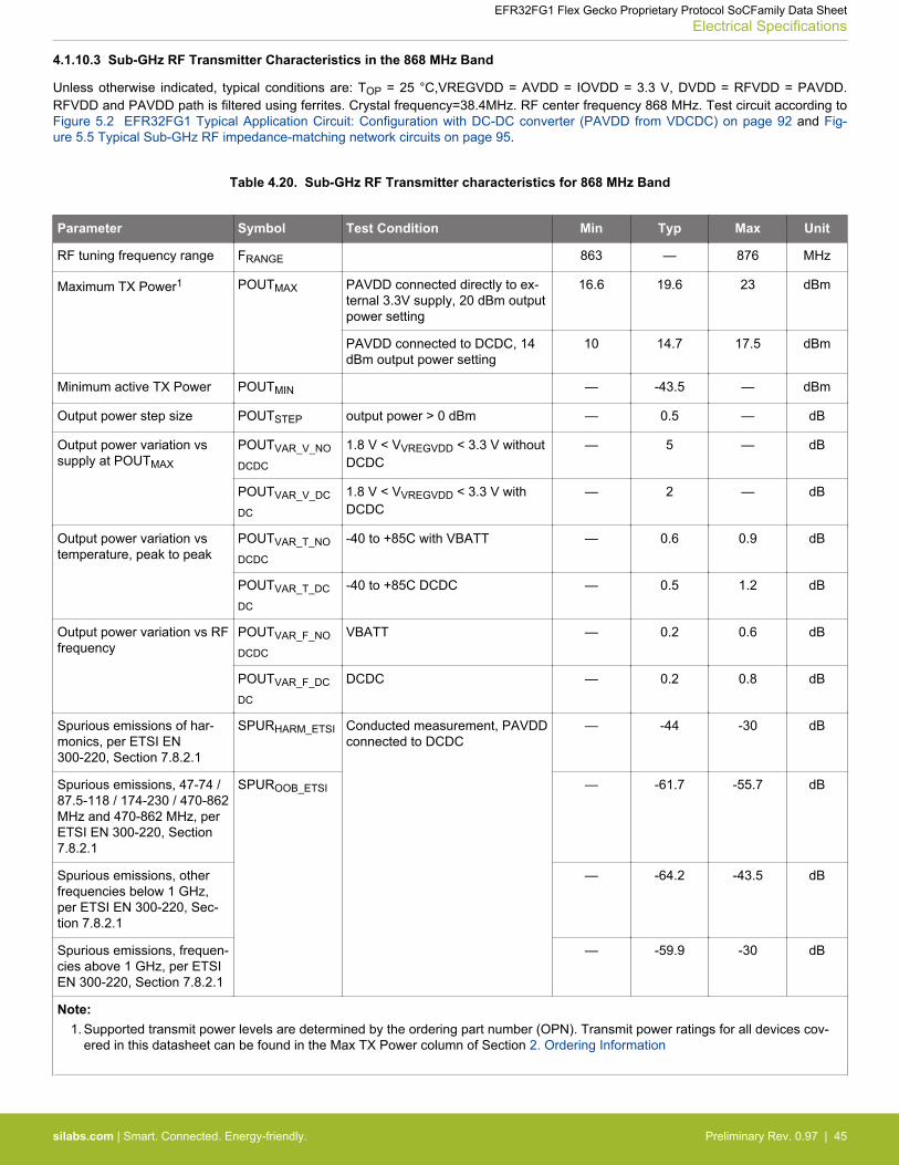
4.1.10.3 Sub-GHz RF Transmitter Characteristics in the 868 MHz Band
Unless otherwise indicated, typical conditions are: TOP = 25 °C,VREGVDD = AVDD = IOVDD = 3.3 V, DVDD = RFVDD = PAVDD.RFVDD and PAVDD path is filtered using ferrites. Crystal frequency=38.4MHz. RF center frequency 868 MHz. Test circuit according toFigure 5.2 EFR32FG1 Typical Application Circuit: Configuration with DC-DC converter (PAVDD from VDCDC) on page 92 and Fig-ure 5.5 Typical Sub-GHz RF impedance-matching network circuits on page 95.
Table 4.20. Sub-GHz RF Transmitter characteristics for 868 MHz Band
Parameter Symbol Test Condition Min Typ Max Unit
RF tuning frequency range FRANGE 863 — 876 MHz
Maximum TX Power1 POUTMAX PAVDD connected directly to ex-ternal 3.3V supply, 20 dBm outputpower setting
16.6 19.6 23 dBm
PAVDD connected to DCDC, 14dBm output power setting
10 14.7 17.5 dBm
Minimum active TX Power POUTMIN — -43.5 — dBm
Output power step size POUTSTEP output power > 0 dBm — 0.5 — dB
Output power variation vssupply at POUTMAX
POUTVAR_V_NO
DCDC
1.8 V < VVREGVDD < 3.3 V withoutDCDC
— 5 — dB
POUTVAR_V_DC
DC
1.8 V < VVREGVDD < 3.3 V withDCDC
— 2 — dB
Output power variation vstemperature, peak to peak
POUTVAR_T_NO
DCDC
-40 to +85C with VBATT — 0.6 0.9 dB
POUTVAR_T_DC
DC
-40 to +85C DCDC — 0.5 1.2 dB
Output power variation vs RFfrequency
POUTVAR_F_NO
DCDC
VBATT — 0.2 0.6 dB
POUTVAR_F_DC
DC
DCDC — 0.2 0.8 dB
Spurious emissions of har-monics, per ETSI EN300-220, Section 7.8.2.1
SPURHARM_ETSI Conducted measurement, PAVDDconnected to DCDC
— -44 -30 dB
Spurious emissions, 47-74 /87.5-118 / 174-230 / 470-862MHz and 470-862 MHz, perETSI EN 300-220, Section7.8.2.1
SPUROOB_ETSI — -61.7 -55.7 dB
Spurious emissions, otherfrequencies below 1 GHz,per ETSI EN 300-220, Sec-tion 7.8.2.1
— -64.2 -43.5 dB
Spurious emissions, frequen-cies above 1 GHz, per ETSIEN 300-220, Section 7.8.2.1
— -59.9 -30 dB
Note:1. Supported transmit power levels are determined by the ordering part number (OPN). Transmit power ratings for all devices cov-
ered in this datasheet can be found in the Max TX Power column of Section 2. Ordering Information
EFR32FG1 Flex Gecko Proprietary Protocol SoCFamily Data SheetElectrical Specifications
silabs.com | Smart. Connected. Energy-friendly. Preliminary Rev. 0.97 | 45
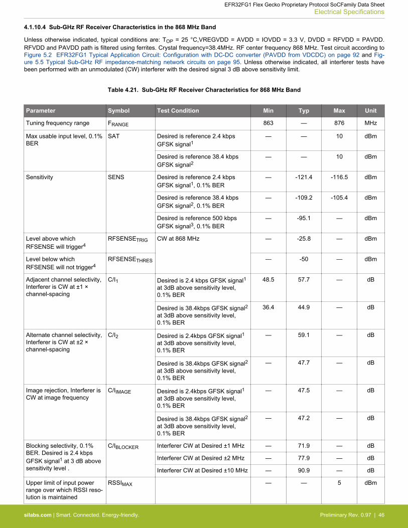
4.1.10.4 Sub-GHz RF Receiver Characteristics in the 868 MHz Band
Unless otherwise indicated, typical conditions are: TOP = 25 °C,VREGVDD = AVDD = IOVDD = 3.3 V, DVDD = RFVDD = PAVDD.RFVDD and PAVDD path is filtered using ferrites. Crystal frequency=38.4MHz. RF center frequency 868 MHz. Test circuit according toFigure 5.2 EFR32FG1 Typical Application Circuit: Configuration with DC-DC converter (PAVDD from VDCDC) on page 92 and Fig-ure 5.5 Typical Sub-GHz RF impedance-matching network circuits on page 95. Unless otherwise indicated, all interferer tests havebeen performed with an unmodulated (CW) interferer with the desired signal 3 dB above sensitivity limit.
Table 4.21. Sub-GHz RF Receiver Characteristics for 868 MHz Band
Parameter Symbol Test Condition Min Typ Max Unit
Tuning frequency range FRANGE 863 — 876 MHz
Max usable input level, 0.1%BER
SAT Desired is reference 2.4 kbpsGFSK signal1
— — 10 dBm
Desired is reference 38.4 kbpsGFSK signal2
— — 10 dBm
Sensitivity SENS Desired is reference 2.4 kbpsGFSK signal1, 0.1% BER
— -121.4 -116.5 dBm
Desired is reference 38.4 kbpsGFSK signal2, 0.1% BER
— -109.2 -105.4 dBm
Desired is reference 500 kbpsGFSK signal3, 0.1% BER
— -95.1 — dBm
Level above whichRFSENSE will trigger4
RFSENSETRIG CW at 868 MHz — -25.8 — dBm
Level below whichRFSENSE will not trigger4
RFSENSETHRES — -50 — dBm
Adjacent channel selectivity,Interferer is CW at ±1 ×channel-spacing
C/I1 Desired is 2.4 kbps GFSK signal1at 3dB above sensitivity level,0.1% BER
48.5 57.7 — dB
Desired is 38.4kbps GFSK signal2at 3dB above sensitivity level,0.1% BER
36.4 44.9 — dB
Alternate channel selectivity,Interferer is CW at ±2 ×channel-spacing
C/I2 Desired is 2.4kbps GFSK signal1at 3dB above sensitivity level,0.1% BER
— 59.1 — dB
Desired is 38.4kbps GFSK signal2at 3dB above sensitivity level,0.1% BER
— 47.7 — dB
Image rejection, Interferer isCW at image frequency
C/IIMAGE Desired is 2.4kbps GFSK signal1at 3dB above sensitivity level,0.1% BER
— 47.5 — dB
Desired is 38.4kbps GFSK signal2at 3dB above sensitivity level,0.1% BER
— 47.2 — dB
Blocking selectivity, 0.1%BER. Desired is 2.4 kbpsGFSK signal1 at 3 dB abovesensitivity level .
C/IBLOCKER Interferer CW at Desired ±1 MHz — 71.9 — dB
Interferer CW at Desired ±2 MHz — 77.9 — dB
Interferer CW at Desired ±10 MHz — 90.9 — dB
Upper limit of input powerrange over which RSSI reso-lution is maintained
RSSIMAX — — 5 dBm
EFR32FG1 Flex Gecko Proprietary Protocol SoCFamily Data SheetElectrical Specifications
silabs.com | Smart. Connected. Energy-friendly. Preliminary Rev. 0.97 | 46
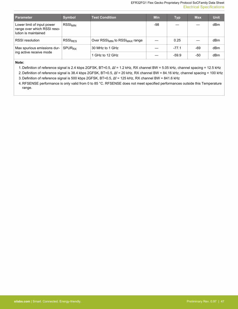
Parameter Symbol Test Condition Min Typ Max Unit
Lower limit of input powerrange over which RSSI reso-lution is maintained
RSSIMIN -98 — — dBm
RSSI resolution RSSIRES Over RSSIMIN to RSSIMAX range — 0.25 — dBm
Max spurious emissions dur-ing active receive mode
SPURRX 30 MHz to 1 GHz — -77.1 -69 dBm
1 GHz to 12 GHz — -59.9 -50 dBm
Note:1. Definition of reference signal is 2.4 kbps 2GFSK, BT=0.5, Δf = 1.2 kHz, RX channel BW = 5.05 kHz, channel spacing = 12.5 kHz2. Definition of reference signal is 38.4 kbps 2GFSK, BT=0.5, Δf = 20 kHz, RX channel BW = 84.16 kHz, channel spacing = 100 kHz3. Definition of reference signal is 500 kbps 2GFSK, BT=0.5, Δf = 125 kHz, RX channel BW = 841.6 kHz4. RFSENSE performance is only valid from 0 to 85 °C. RFSENSE does not meet specified performances outside this Temperature
range.
EFR32FG1 Flex Gecko Proprietary Protocol SoCFamily Data SheetElectrical Specifications
silabs.com | Smart. Connected. Energy-friendly. Preliminary Rev. 0.97 | 47
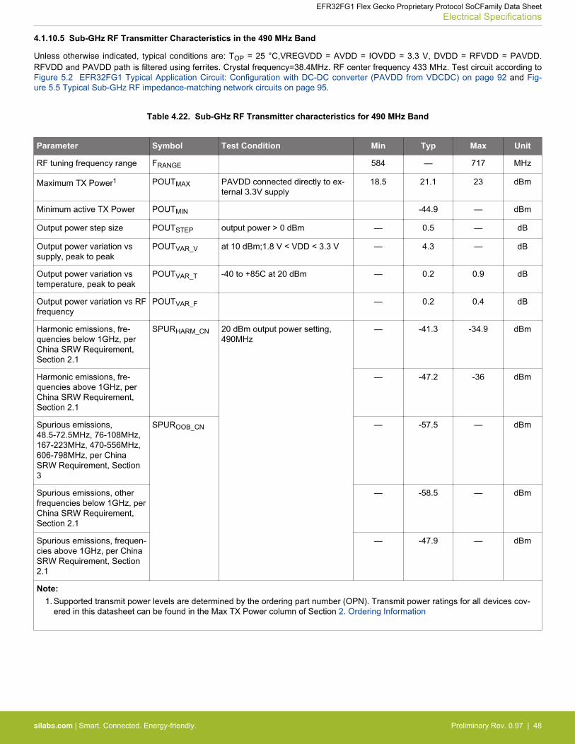
4.1.10.5 Sub-GHz RF Transmitter Characteristics in the 490 MHz Band
Unless otherwise indicated, typical conditions are: TOP = 25 °C,VREGVDD = AVDD = IOVDD = 3.3 V, DVDD = RFVDD = PAVDD.RFVDD and PAVDD path is filtered using ferrites. Crystal frequency=38.4MHz. RF center frequency 433 MHz. Test circuit according toFigure 5.2 EFR32FG1 Typical Application Circuit: Configuration with DC-DC converter (PAVDD from VDCDC) on page 92 and Fig-ure 5.5 Typical Sub-GHz RF impedance-matching network circuits on page 95.
Table 4.22. Sub-GHz RF Transmitter characteristics for 490 MHz Band
Parameter Symbol Test Condition Min Typ Max Unit
RF tuning frequency range FRANGE 584 — 717 MHz
Maximum TX Power1 POUTMAX PAVDD connected directly to ex-ternal 3.3V supply
18.5 21.1 23 dBm
Minimum active TX Power POUTMIN -44.9 — dBm
Output power step size POUTSTEP output power > 0 dBm — 0.5 — dB
Output power variation vssupply, peak to peak
POUTVAR_V at 10 dBm;1.8 V < VDD < 3.3 V — 4.3 — dB
Output power variation vstemperature, peak to peak
POUTVAR_T -40 to +85C at 20 dBm — 0.2 0.9 dB
Output power variation vs RFfrequency
POUTVAR_F — 0.2 0.4 dB
Harmonic emissions, fre-quencies below 1GHz, perChina SRW Requirement,Section 2.1
SPURHARM_CN 20 dBm output power setting,490MHz
— -41.3 -34.9 dBm
Harmonic emissions, fre-quencies above 1GHz, perChina SRW Requirement,Section 2.1
— -47.2 -36 dBm
Spurious emissions,48.5-72.5MHz, 76-108MHz,167-223MHz, 470-556MHz,606-798MHz, per ChinaSRW Requirement, Section3
SPUROOB_CN — -57.5 — dBm
Spurious emissions, otherfrequencies below 1GHz, perChina SRW Requirement,Section 2.1
— -58.5 — dBm
Spurious emissions, frequen-cies above 1GHz, per ChinaSRW Requirement, Section2.1
— -47.9 — dBm
Note:1. Supported transmit power levels are determined by the ordering part number (OPN). Transmit power ratings for all devices cov-
ered in this datasheet can be found in the Max TX Power column of Section 2. Ordering Information
EFR32FG1 Flex Gecko Proprietary Protocol SoCFamily Data SheetElectrical Specifications
silabs.com | Smart. Connected. Energy-friendly. Preliminary Rev. 0.97 | 48
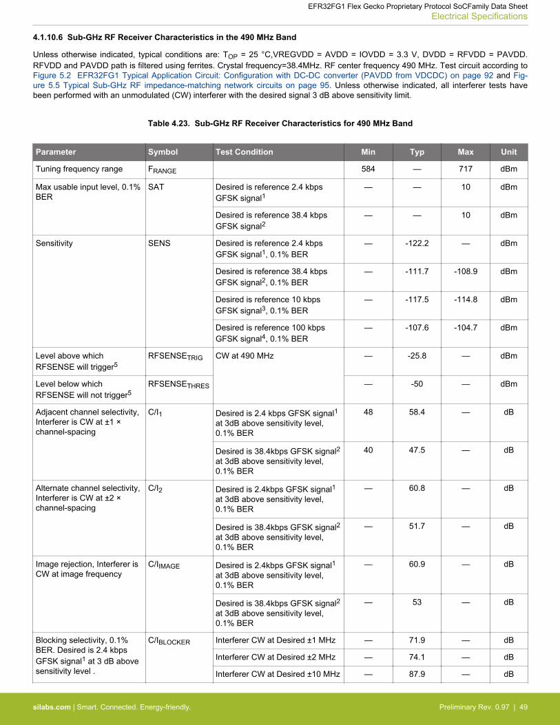
4.1.10.6 Sub-GHz RF Receiver Characteristics in the 490 MHz Band
Unless otherwise indicated, typical conditions are: TOP = 25 °C,VREGVDD = AVDD = IOVDD = 3.3 V, DVDD = RFVDD = PAVDD.RFVDD and PAVDD path is filtered using ferrites. Crystal frequency=38.4MHz. RF center frequency 490 MHz. Test circuit according toFigure 5.2 EFR32FG1 Typical Application Circuit: Configuration with DC-DC converter (PAVDD from VDCDC) on page 92 and Fig-ure 5.5 Typical Sub-GHz RF impedance-matching network circuits on page 95. Unless otherwise indicated, all interferer tests havebeen performed with an unmodulated (CW) interferer with the desired signal 3 dB above sensitivity limit.
Table 4.23. Sub-GHz RF Receiver Characteristics for 490 MHz Band
Parameter Symbol Test Condition Min Typ Max Unit
Tuning frequency range FRANGE 584 — 717 dBm
Max usable input level, 0.1%BER
SAT Desired is reference 2.4 kbpsGFSK signal1
— — 10 dBm
Desired is reference 38.4 kbpsGFSK signal2
— — 10 dBm
Sensitivity SENS Desired is reference 2.4 kbpsGFSK signal1, 0.1% BER
— -122.2 — dBm
Desired is reference 38.4 kbpsGFSK signal2, 0.1% BER
— -111.7 -108.9 dBm
Desired is reference 10 kbpsGFSK signal3, 0.1% BER
— -117.5 -114.8 dBm
Desired is reference 100 kbpsGFSK signal4, 0.1% BER
— -107.6 -104.7 dBm
Level above whichRFSENSE will trigger5
RFSENSETRIG CW at 490 MHz — -25.8 — dBm
Level below whichRFSENSE will not trigger5
RFSENSETHRES — -50 — dBm
Adjacent channel selectivity,Interferer is CW at ±1 ×channel-spacing
C/I1 Desired is 2.4 kbps GFSK signal1at 3dB above sensitivity level,0.1% BER
48 58.4 — dB
Desired is 38.4kbps GFSK signal2at 3dB above sensitivity level,0.1% BER
40 47.5 — dB
Alternate channel selectivity,Interferer is CW at ±2 ×channel-spacing
C/I2 Desired is 2.4kbps GFSK signal1at 3dB above sensitivity level,0.1% BER
— 60.8 — dB
Desired is 38.4kbps GFSK signal2at 3dB above sensitivity level,0.1% BER
— 51.7 — dB
Image rejection, Interferer isCW at image frequency
C/IIMAGE Desired is 2.4kbps GFSK signal1at 3dB above sensitivity level,0.1% BER
— 60.9 — dB
Desired is 38.4kbps GFSK signal2at 3dB above sensitivity level,0.1% BER
— 53 — dB
Blocking selectivity, 0.1%BER. Desired is 2.4 kbpsGFSK signal1 at 3 dB abovesensitivity level .
C/IBLOCKER Interferer CW at Desired ±1 MHz — 71.9 — dB
Interferer CW at Desired ±2 MHz — 74.1 — dB
Interferer CW at Desired ±10 MHz — 87.9 — dB
EFR32FG1 Flex Gecko Proprietary Protocol SoCFamily Data SheetElectrical Specifications
silabs.com | Smart. Connected. Energy-friendly. Preliminary Rev. 0.97 | 49
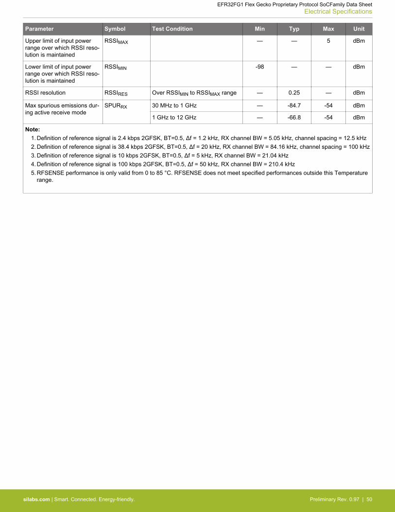
Parameter Symbol Test Condition Min Typ Max Unit
Upper limit of input powerrange over which RSSI reso-lution is maintained
RSSIMAX — — 5 dBm
Lower limit of input powerrange over which RSSI reso-lution is maintained
RSSIMIN -98 — — dBm
RSSI resolution RSSIRES Over RSSIMIN to RSSIMAX range — 0.25 — dBm
Max spurious emissions dur-ing active receive mode
SPURRX 30 MHz to 1 GHz — -84.7 -54 dBm
1 GHz to 12 GHz — -66.8 -54 dBm
Note:1. Definition of reference signal is 2.4 kbps 2GFSK, BT=0.5, Δf = 1.2 kHz, RX channel BW = 5.05 kHz, channel spacing = 12.5 kHz2. Definition of reference signal is 38.4 kbps 2GFSK, BT=0.5, Δf = 20 kHz, RX channel BW = 84.16 kHz, channel spacing = 100 kHz3. Definition of reference signal is 10 kbps 2GFSK, BT=0.5, Δf = 5 kHz, RX channel BW = 21.04 kHz4. Definition of reference signal is 100 kbps 2GFSK, BT=0.5, Δf = 50 kHz, RX channel BW = 210.4 kHz5. RFSENSE performance is only valid from 0 to 85 °C. RFSENSE does not meet specified performances outside this Temperature
range.
EFR32FG1 Flex Gecko Proprietary Protocol SoCFamily Data SheetElectrical Specifications
silabs.com | Smart. Connected. Energy-friendly. Preliminary Rev. 0.97 | 50
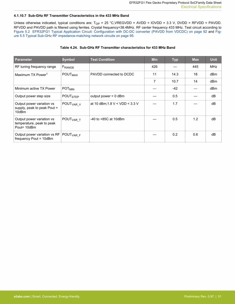
4.1.10.7 Sub-GHz RF Transmitter Characteristics in the 433 MHz Band
Unless otherwise indicated, typical conditions are: TOP = 25 °C,VREGVDD = AVDD = IOVDD = 3.3 V, DVDD = RFVDD = PAVDD.RFVDD and PAVDD path is filtered using ferrites. Crystal frequency=38.4MHz. RF center frequency 433 MHz. Test circuit according toFigure 5.2 EFR32FG1 Typical Application Circuit: Configuration with DC-DC converter (PAVDD from VDCDC) on page 92 and Fig-ure 5.5 Typical Sub-GHz RF impedance-matching network circuits on page 95.
Table 4.24. Sub-GHz RF Transmitter characteristics for 433 MHz Band
Parameter Symbol Test Condition Min Typ Max Unit
RF tuning frequency range FRANGE 426 — 445 MHz
Maximum TX Power1 POUTMAX PAVDD connected to DCDC 11 14.3 18 dBm
7 10.7 14 dBm
Minimum active TX Power POTMIN — -42 — dBm
Output power step size POUTSTEP output power > 0 dBm — 0.5 — dB
Output power variation vssupply, peak to peak Pout =10dBm
POUTVAR_V at 10 dBm;1.8 V < VDD < 3.3 V — 1.7 — dB
Output power variation vstemperature, peak to peakPout= 10dBm
POUTVAR_T -40 to +85C at 10dBm — 0.5 1.2 dB
Output power variation vs RFfrequency Pout = 10dBm
POUTVAR_F — 0.2 0.6 dB
EFR32FG1 Flex Gecko Proprietary Protocol SoCFamily Data SheetElectrical Specifications
silabs.com | Smart. Connected. Energy-friendly. Preliminary Rev. 0.97 | 51
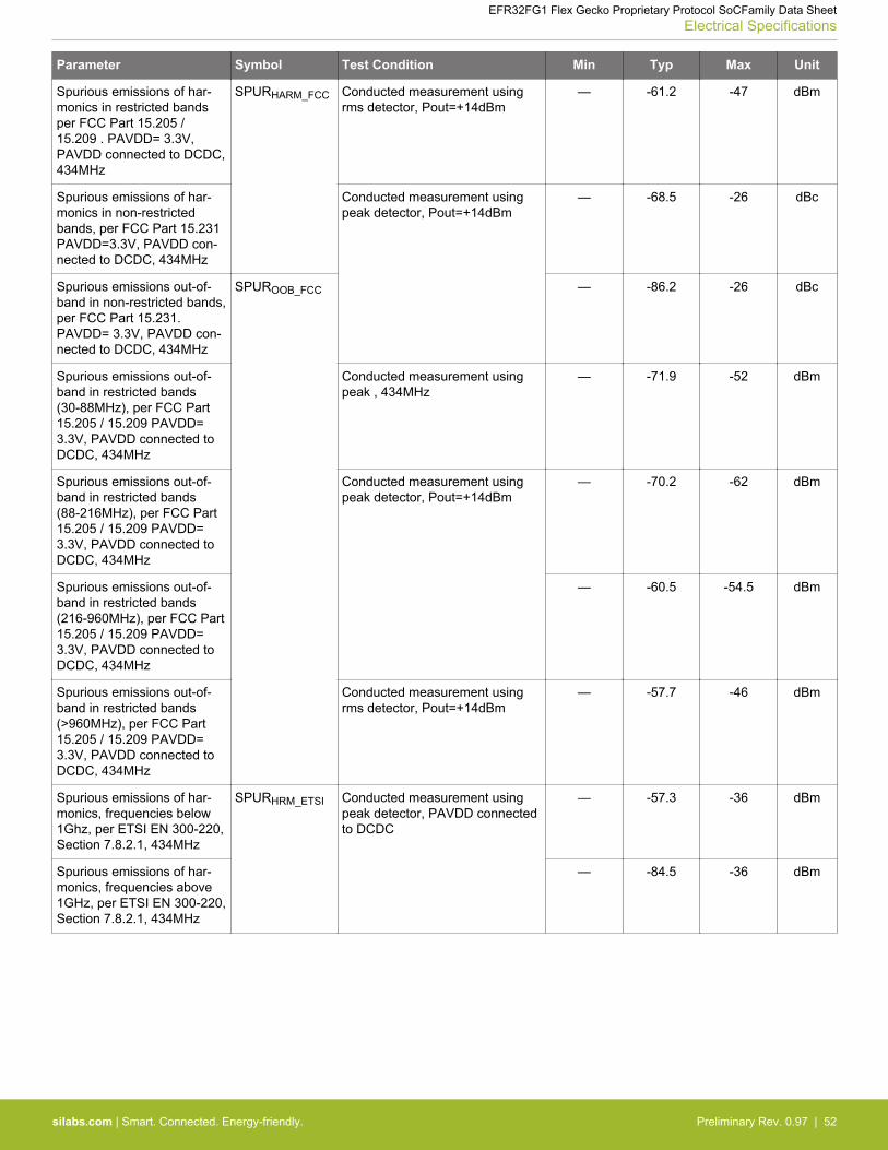
Parameter Symbol Test Condition Min Typ Max Unit
Spurious emissions of har-monics in restricted bandsper FCC Part 15.205 /15.209 . PAVDD= 3.3V,PAVDD connected to DCDC,434MHz
SPURHARM_FCC Conducted measurement usingrms detector, Pout=+14dBm
— -61.2 -47 dBm
Spurious emissions of har-monics in non-restrictedbands, per FCC Part 15.231PAVDD=3.3V, PAVDD con-nected to DCDC, 434MHz
Conducted measurement usingpeak detector, Pout=+14dBm
— -68.5 -26 dBc
Spurious emissions out-of-band in non-restricted bands,per FCC Part 15.231.PAVDD= 3.3V, PAVDD con-nected to DCDC, 434MHz
SPUROOB_FCC — -86.2 -26 dBc
Spurious emissions out-of-band in restricted bands(30-88MHz), per FCC Part15.205 / 15.209 PAVDD=3.3V, PAVDD connected toDCDC, 434MHz
Conducted measurement usingpeak , 434MHz
— -71.9 -52 dBm
Spurious emissions out-of-band in restricted bands(88-216MHz), per FCC Part15.205 / 15.209 PAVDD=3.3V, PAVDD connected toDCDC, 434MHz
Conducted measurement usingpeak detector, Pout=+14dBm
— -70.2 -62 dBm
Spurious emissions out-of-band in restricted bands(216-960MHz), per FCC Part15.205 / 15.209 PAVDD=3.3V, PAVDD connected toDCDC, 434MHz
— -60.5 -54.5 dBm
Spurious emissions out-of-band in restricted bands(>960MHz), per FCC Part15.205 / 15.209 PAVDD=3.3V, PAVDD connected toDCDC, 434MHz
Conducted measurement usingrms detector, Pout=+14dBm
— -57.7 -46 dBm
Spurious emissions of har-monics, frequencies below1Ghz, per ETSI EN 300-220,Section 7.8.2.1, 434MHz
SPURHRM_ETSI Conducted measurement usingpeak detector, PAVDD connectedto DCDC
— -57.3 -36 dBm
Spurious emissions of har-monics, frequencies above1GHz, per ETSI EN 300-220,Section 7.8.2.1, 434MHz
— -84.5 -36 dBm
EFR32FG1 Flex Gecko Proprietary Protocol SoCFamily Data SheetElectrical Specifications
silabs.com | Smart. Connected. Energy-friendly. Preliminary Rev. 0.97 | 52
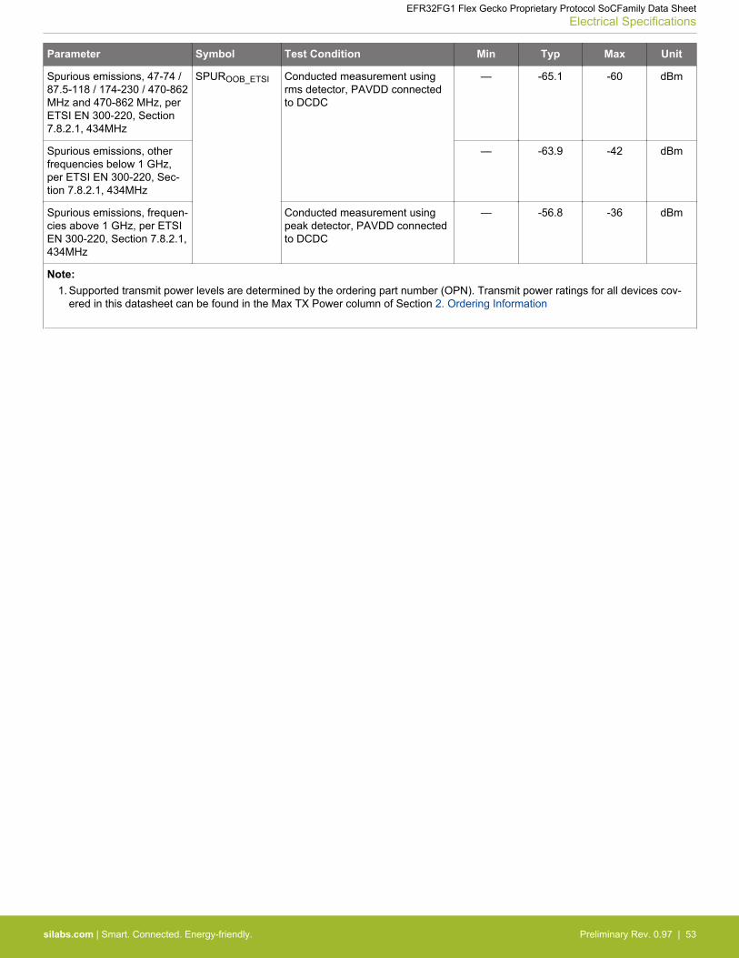
Parameter Symbol Test Condition Min Typ Max Unit
Spurious emissions, 47-74 /87.5-118 / 174-230 / 470-862MHz and 470-862 MHz, perETSI EN 300-220, Section7.8.2.1, 434MHz
SPUROOB_ETSI Conducted measurement usingrms detector, PAVDD connectedto DCDC
— -65.1 -60 dBm
Spurious emissions, otherfrequencies below 1 GHz,per ETSI EN 300-220, Sec-tion 7.8.2.1, 434MHz
— -63.9 -42 dBm
Spurious emissions, frequen-cies above 1 GHz, per ETSIEN 300-220, Section 7.8.2.1,434MHz
Conducted measurement usingpeak detector, PAVDD connectedto DCDC
— -56.8 -36 dBm
Note:1. Supported transmit power levels are determined by the ordering part number (OPN). Transmit power ratings for all devices cov-
ered in this datasheet can be found in the Max TX Power column of Section 2. Ordering Information
EFR32FG1 Flex Gecko Proprietary Protocol SoCFamily Data SheetElectrical Specifications
silabs.com | Smart. Connected. Energy-friendly. Preliminary Rev. 0.97 | 53
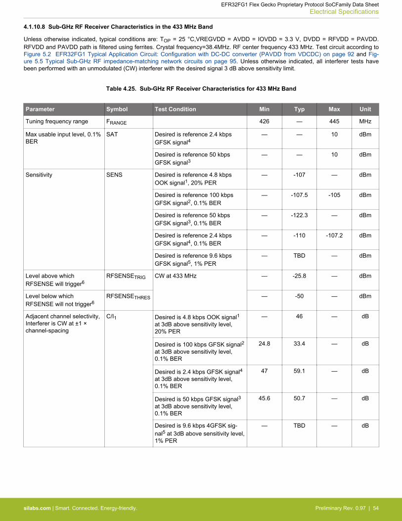
4.1.10.8 Sub-GHz RF Receiver Characteristics in the 433 MHz Band
Unless otherwise indicated, typical conditions are: TOP = 25 °C,VREGVDD = AVDD = IOVDD = 3.3 V, DVDD = RFVDD = PAVDD.RFVDD and PAVDD path is filtered using ferrites. Crystal frequency=38.4MHz. RF center frequency 433 MHz. Test circuit according toFigure 5.2 EFR32FG1 Typical Application Circuit: Configuration with DC-DC converter (PAVDD from VDCDC) on page 92 and Fig-ure 5.5 Typical Sub-GHz RF impedance-matching network circuits on page 95. Unless otherwise indicated, all interferer tests havebeen performed with an unmodulated (CW) interferer with the desired signal 3 dB above sensitivity limit.
Table 4.25. Sub-GHz RF Receiver Characteristics for 433 MHz Band
Parameter Symbol Test Condition Min Typ Max Unit
Tuning frequency range FRANGE 426 — 445 MHz
Max usable input level, 0.1%BER
SAT Desired is reference 2.4 kbpsGFSK signal4
— — 10 dBm
Desired is reference 50 kbpsGFSK signal3
— — 10 dBm
Sensitivity SENS Desired is reference 4.8 kbpsOOK signal1, 20% PER
— -107 — dBm
Desired is reference 100 kbpsGFSK signal2, 0.1% BER
— -107.5 -105 dBm
Desired is reference 50 kbpsGFSK signal3, 0.1% BER
— -122.3 — dBm
Desired is reference 2.4 kbpsGFSK signal4, 0.1% BER
— -110 -107.2 dBm
Desired is reference 9.6 kbpsGFSK signal5, 1% PER
— TBD — dBm
Level above whichRFSENSE will trigger6
RFSENSETRIG CW at 433 MHz — -25.8 — dBm
Level below whichRFSENSE will not trigger6
RFSENSETHRES — -50 — dBm
Adjacent channel selectivity,Interferer is CW at ±1 ×channel-spacing
C/I1 Desired is 4.8 kbps OOK signal1at 3dB above sensitivity level,20% PER
— 46 — dB
Desired is 100 kbps GFSK signal2at 3dB above sensitivity level,0.1% BER
24.8 33.4 — dB
Desired is 2.4 kbps GFSK signal4at 3dB above sensitivity level,0.1% BER
47 59.1 — dB
Desired is 50 kbps GFSK signal3at 3dB above sensitivity level,0.1% BER
45.6 50.7 — dB
Desired is 9.6 kbps 4GFSK sig-nal5 at 3dB above sensitivity level,1% PER
— TBD — dB
EFR32FG1 Flex Gecko Proprietary Protocol SoCFamily Data SheetElectrical Specifications
silabs.com | Smart. Connected. Energy-friendly. Preliminary Rev. 0.97 | 54
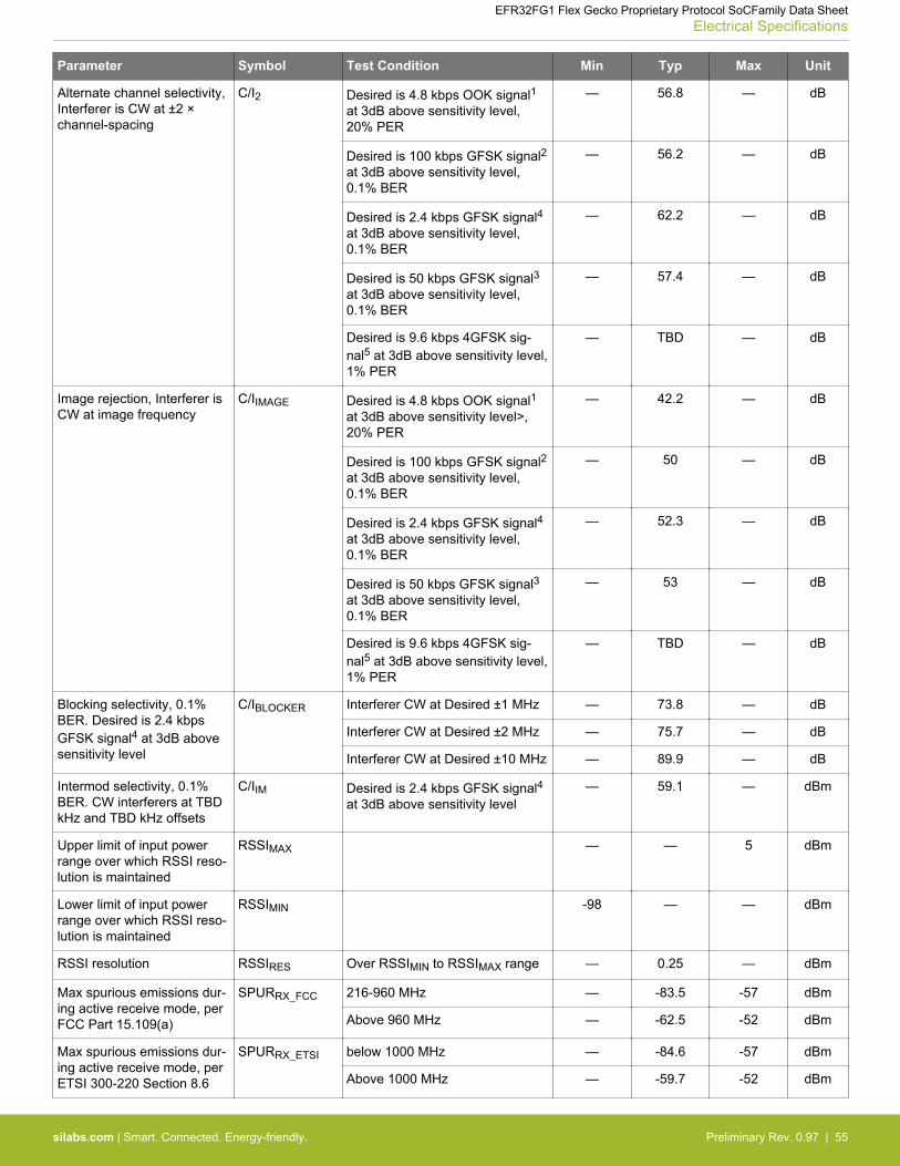
Parameter Symbol Test Condition Min Typ Max Unit
Alternate channel selectivity,Interferer is CW at ±2 ×channel-spacing
C/I2 Desired is 4.8 kbps OOK signal1at 3dB above sensitivity level,20% PER
— 56.8 — dB
Desired is 100 kbps GFSK signal2at 3dB above sensitivity level,0.1% BER
— 56.2 — dB
Desired is 2.4 kbps GFSK signal4at 3dB above sensitivity level,0.1% BER
— 62.2 — dB
Desired is 50 kbps GFSK signal3at 3dB above sensitivity level,0.1% BER
— 57.4 — dB
Desired is 9.6 kbps 4GFSK sig-nal5 at 3dB above sensitivity level,1% PER
— TBD — dB
Image rejection, Interferer isCW at image frequency
C/IIMAGE Desired is 4.8 kbps OOK signal1at 3dB above sensitivity level>,20% PER
— 42.2 — dB
Desired is 100 kbps GFSK signal2at 3dB above sensitivity level,0.1% BER
— 50 — dB
Desired is 2.4 kbps GFSK signal4at 3dB above sensitivity level,0.1% BER
— 52.3 — dB
Desired is 50 kbps GFSK signal3at 3dB above sensitivity level,0.1% BER
— 53 — dB
Desired is 9.6 kbps 4GFSK sig-nal5 at 3dB above sensitivity level,1% PER
— TBD — dB
Blocking selectivity, 0.1%BER. Desired is 2.4 kbpsGFSK signal4 at 3dB abovesensitivity level
C/IBLOCKER Interferer CW at Desired ±1 MHz — 73.8 — dB
Interferer CW at Desired ±2 MHz — 75.7 — dB
Interferer CW at Desired ±10 MHz — 89.9 — dB
Intermod selectivity, 0.1%BER. CW interferers at TBDkHz and TBD kHz offsets
C/IIM Desired is 2.4 kbps GFSK signal4at 3dB above sensitivity level
— 59.1 — dBm
Upper limit of input powerrange over which RSSI reso-lution is maintained
RSSIMAX — — 5 dBm
Lower limit of input powerrange over which RSSI reso-lution is maintained
RSSIMIN -98 — — dBm
RSSI resolution RSSIRES Over RSSIMIN to RSSIMAX range — 0.25 — dBm
Max spurious emissions dur-ing active receive mode, perFCC Part 15.109(a)
SPURRX_FCC 216-960 MHz — -83.5 -57 dBm
Above 960 MHz — -62.5 -52 dBm
Max spurious emissions dur-ing active receive mode, perETSI 300-220 Section 8.6
SPURRX_ETSI below 1000 MHz — -84.6 -57 dBm
Above 1000 MHz — -59.7 -52 dBm
EFR32FG1 Flex Gecko Proprietary Protocol SoCFamily Data SheetElectrical Specifications
silabs.com | Smart. Connected. Energy-friendly. Preliminary Rev. 0.97 | 55
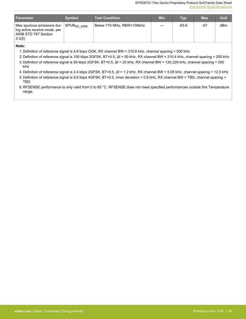
Parameter Symbol Test Condition Min Typ Max Unit
Max spurious emissions dur-ing active receive mode, perARIB STD T67 Section3.3(5)
SPURRX_ARIB Below 710 MHz, RBW=100kHz — -83.6 -57 dBm
Note:1. Definition of reference signal is 4.8 kbps OOK, RX channel BW = 315.6 kHz, channel spacing = 500 kHz2. Definition of reference signal is 100 kbps 2GFSK, BT=0.5, Δf = 50 kHz, RX channel BW = 210.4 kHz, channel spacing = 200 kHz3. Definition of reference signal is 50 kbps 2GFSK, BT=0.5, Δf = 25 kHz, RX channel BW = 120.229 kHz, channel spacing = 200
kHz4. Definition of reference signal is 2.4 kbps 2GFSK, BT=0.5, Δf = 1.2 kHz, RX channel BW = 5.05 kHz, channel spacing = 12.5 kHz5. Definition of reference signal is 9.6 kbps 4GFSK, BT=0.5, inner deviation = 0.8 kHz, RX channel BW = TBD, channel spacing =
TBD6. RFSENSE performance is only valid from 0 to 85 °C. RFSENSE does not meet specified performances outside this Temperature
range.
EFR32FG1 Flex Gecko Proprietary Protocol SoCFamily Data SheetElectrical Specifications
silabs.com | Smart. Connected. Energy-friendly. Preliminary Rev. 0.97 | 56
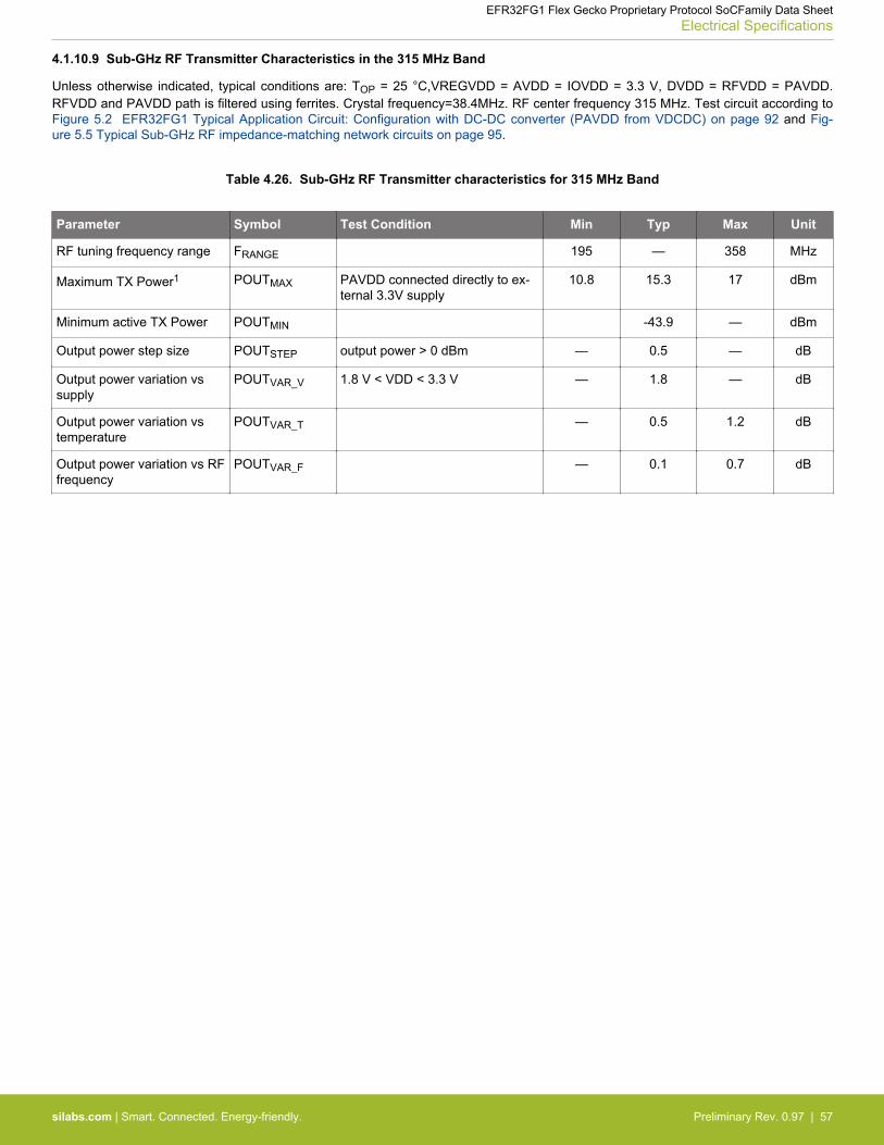
4.1.10.9 Sub-GHz RF Transmitter Characteristics in the 315 MHz Band
Unless otherwise indicated, typical conditions are: TOP = 25 °C,VREGVDD = AVDD = IOVDD = 3.3 V, DVDD = RFVDD = PAVDD.RFVDD and PAVDD path is filtered using ferrites. Crystal frequency=38.4MHz. RF center frequency 315 MHz. Test circuit according toFigure 5.2 EFR32FG1 Typical Application Circuit: Configuration with DC-DC converter (PAVDD from VDCDC) on page 92 and Fig-ure 5.5 Typical Sub-GHz RF impedance-matching network circuits on page 95.
Table 4.26. Sub-GHz RF Transmitter characteristics for 315 MHz Band
Parameter Symbol Test Condition Min Typ Max Unit
RF tuning frequency range FRANGE 195 — 358 MHz
Maximum TX Power1 POUTMAX PAVDD connected directly to ex-ternal 3.3V supply
10.8 15.3 17 dBm
Minimum active TX Power POUTMIN -43.9 — dBm
Output power step size POUTSTEP output power > 0 dBm — 0.5 — dB
Output power variation vssupply
POUTVAR_V 1.8 V < VDD < 3.3 V — 1.8 — dB
Output power variation vstemperature
POUTVAR_T — 0.5 1.2 dB
Output power variation vs RFfrequency
POUTVAR_F — 0.1 0.7 dB
EFR32FG1 Flex Gecko Proprietary Protocol SoCFamily Data SheetElectrical Specifications
silabs.com | Smart. Connected. Energy-friendly. Preliminary Rev. 0.97 | 57
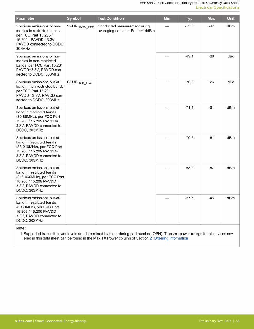
Parameter Symbol Test Condition Min Typ Max Unit
Spurious emissions of har-monics in restricted bands,per FCC Part 15.205 /15.209 . PAVDD= 3.3V,PAVDD connected to DCDC,303MHz
SPURHARM_FCC Conducted measurement usingaveraging detector, Pout=+14dBm
— -53.8 -47 dBm
Spurious emissions of har-monics in non-restrictedbands, per FCC Part 15.231PAVDD=3.3V, PAVDD con-nected to DCDC, 303MHz
— -63.4 -26 dBc
Spurious emissions out-of-band in non-restricted bands,per FCC Part 15.231.PAVDD= 3.3V, PAVDD con-nected to DCDC, 303MHz
SPUROOB_FCC — -76.6 -26 dBc
Spurious emissions out-of-band in restricted bands(30-88MHz), per FCC Part15.205 / 15.209 PAVDD=3.3V, PAVDD connected toDCDC, 303MHz
— -71.8 -51 dBm
Spurious emissions out-of-band in restricted bands(88-216MHz), per FCC Part15.205 / 15.209 PAVDD=3.3V, PAVDD connected toDCDC, 303MHz
— -70.2 -61 dBm
Spurious emissions out-of-band in restricted bands(216-960MHz), per FCC Part15.205 / 15.209 PAVDD=3.3V, PAVDD connected toDCDC, 303MHz
— -68.2 -57 dBm
Spurious emissions out-of-band in restricted bands(>960MHz), per FCC Part15.205 / 15.209 PAVDD=3.3V, PAVDD connected toDCDC, 303MHz
— -57.5 -46 dBm
Note:1. Supported transmit power levels are determined by the ordering part number (OPN). Transmit power ratings for all devices cov-
ered in this datasheet can be found in the Max TX Power column of Section 2. Ordering Information
EFR32FG1 Flex Gecko Proprietary Protocol SoCFamily Data SheetElectrical Specifications
silabs.com | Smart. Connected. Energy-friendly. Preliminary Rev. 0.97 | 58
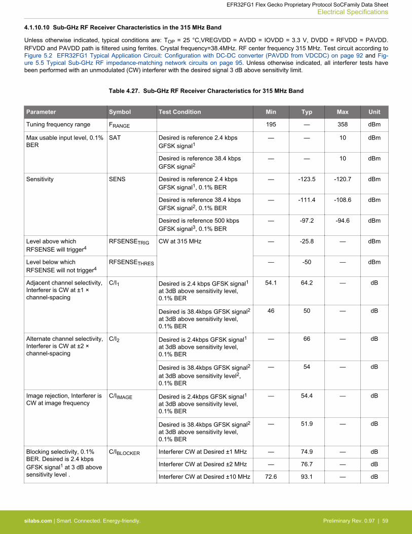
4.1.10.10 Sub-GHz RF Receiver Characteristics in the 315 MHz Band
Unless otherwise indicated, typical conditions are: TOP = 25 °C,VREGVDD = AVDD = IOVDD = 3.3 V, DVDD = RFVDD = PAVDD.RFVDD and PAVDD path is filtered using ferrites. Crystal frequency=38.4MHz. RF center frequency 315 MHz. Test circuit according toFigure 5.2 EFR32FG1 Typical Application Circuit: Configuration with DC-DC converter (PAVDD from VDCDC) on page 92 and Fig-ure 5.5 Typical Sub-GHz RF impedance-matching network circuits on page 95. Unless otherwise indicated, all interferer tests havebeen performed with an unmodulated (CW) interferer with the desired signal 3 dB above sensitivity limit.
Table 4.27. Sub-GHz RF Receiver Characteristics for 315 MHz Band
Parameter Symbol Test Condition Min Typ Max Unit
Tuning frequency range FRANGE 195 — 358 dBm
Max usable input level, 0.1%BER
SAT Desired is reference 2.4 kbpsGFSK signal1
— — 10 dBm
Desired is reference 38.4 kbpsGFSK signal2
— — 10 dBm
Sensitivity SENS Desired is reference 2.4 kbpsGFSK signal1, 0.1% BER
— -123.5 -120.7 dBm
Desired is reference 38.4 kbpsGFSK signal2, 0.1% BER
— -111.4 -108.6 dBm
Desired is reference 500 kbpsGFSK signal3, 0.1% BER
— -97.2 -94.6 dBm
Level above whichRFSENSE will trigger4
RFSENSETRIG CW at 315 MHz — -25.8 — dBm
Level below whichRFSENSE will not trigger4
RFSENSETHRES — -50 — dBm
Adjacent channel selectivity,Interferer is CW at ±1 ×channel-spacing
C/I1 Desired is 2.4 kbps GFSK signal1at 3dB above sensitivity level,0.1% BER
54.1 64.2 — dB
Desired is 38.4kbps GFSK signal2at 3dB above sensitivity level,0.1% BER
46 50 — dB
Alternate channel selectivity,Interferer is CW at ±2 ×channel-spacing
C/I2 Desired is 2.4kbps GFSK signal1at 3dB above sensitivity level,0.1% BER
— 66 — dB
Desired is 38.4kbps GFSK signal2
at 3dB above sensitivity level2,0.1% BER
— 54 — dB
Image rejection, Interferer isCW at image frequency
C/IIMAGE Desired is 2.4kbps GFSK signal1at 3dB above sensitivity level,0.1% BER
— 54.4 — dB
Desired is 38.4kbps GFSK signal2at 3dB above sensitivity level,0.1% BER
— 51.9 — dB
Blocking selectivity, 0.1%BER. Desired is 2.4 kbpsGFSK signal1 at 3 dB abovesensitivity level .
C/IBLOCKER Interferer CW at Desired ±1 MHz — 74.9 — dB
Interferer CW at Desired ±2 MHz — 76.7 — dB
Interferer CW at Desired ±10 MHz 72.6 93.1 — dB
EFR32FG1 Flex Gecko Proprietary Protocol SoCFamily Data SheetElectrical Specifications
silabs.com | Smart. Connected. Energy-friendly. Preliminary Rev. 0.97 | 59

Parameter Symbol Test Condition Min Typ Max Unit
Upper limit of input powerrange over which RSSI reso-lution is maintained
RSSIMAX — — 5 dBm
Lower limit of input powerrange over which RSSI reso-lution is maintained
RSSIMIN -98 — — dBm
RSSI resolution RSSIRES Over RSSIMIN to RSSIMAX range — 0.25 — dBm
Max spurious emissions dur-ing active receive mode
SPURRX FCC 216 to 960 MHz — -87.4 -55 dBm
FCC >960MHz — -76.7 -47 dBm
Note:1. Definition of reference signal is 2.4 kbps 2GFSK, BT=0.5, Δf = 1.2 kHz, RX channel BW = 5.05 kHz, channel spacing = 12.5 kHz2. Definition of reference signal is 38.4 kbps 2GFSK, BT=0.5, Δf = 20 kHz, RX channel BW = 84.16 kHz, channel spacing = 100 kHz3. Definition of reference signal is 500 kbps 2GFSK, BT=0.5, Δf = 125 kHz, RX channel BW = 841.6 kHz4. RFSENSE performance is only valid from 0 to 85 °C. RFSENSE does not meet specified performances outside this Temperature
range.
EFR32FG1 Flex Gecko Proprietary Protocol SoCFamily Data SheetElectrical Specifications
silabs.com | Smart. Connected. Energy-friendly. Preliminary Rev. 0.97 | 60
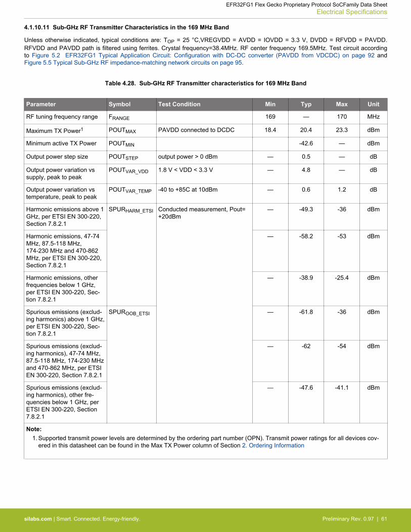
4.1.10.11 Sub-GHz RF Transmitter Characteristics in the 169 MHz Band
Unless otherwise indicated, typical conditions are: TOP = 25 °C,VREGVDD = AVDD = IOVDD = 3.3 V, DVDD = RFVDD = PAVDD.RFVDD and PAVDD path is filtered using ferrites. Crystal frequency=38.4MHz. RF center frequency 169.5MHz. Test circuit accordingto Figure 5.2 EFR32FG1 Typical Application Circuit: Configuration with DC-DC converter (PAVDD from VDCDC) on page 92 andFigure 5.5 Typical Sub-GHz RF impedance-matching network circuits on page 95.
Table 4.28. Sub-GHz RF Transmitter characteristics for 169 MHz Band
Parameter Symbol Test Condition Min Typ Max Unit
RF tuning frequency range FRANGE 169 — 170 MHz
Maximum TX Power1 POUTMAX PAVDD connected to DCDC 18.4 20.4 23.3 dBm
Minimum active TX Power POUTMIN -42.6 — dBm
Output power step size POUTSTEP output power > 0 dBm — 0.5 — dB
Output power variation vssupply, peak to peak
POUTVAR_VDD 1.8 V < VDD < 3.3 V — 4.8 — dB
Output power variation vstemperature, peak to peak
POUTVAR_TEMP -40 to +85C at 10dBm — 0.6 1.2 dB
Harmonic emissions above 1GHz, per ETSI EN 300-220,Section 7.8.2.1
SPURHARM_ETSI Conducted measurement, Pout=+20dBm
— -49.3 -36 dBm
Harmonic emissions, 47-74MHz, 87.5-118 MHz,174-230 MHz and 470-862MHz, per ETSI EN 300-220,Section 7.8.2.1
— -58.2 -53 dBm
Harmonic emissions, otherfrequencies below 1 GHz,per ETSI EN 300-220, Sec-tion 7.8.2.1
— -38.9 -25.4 dBm
Spurious emissions (exclud-ing harmonics) above 1 GHz,per ETSI EN 300-220, Sec-tion 7.8.2.1
SPUROOB_ETSI — -61.8 -36 dBm
Spurious emissions (exclud-ing harmonics), 47-74 MHz,87.5-118 MHz, 174-230 MHzand 470-862 MHz, per ETSIEN 300-220, Section 7.8.2.1
— -62 -54 dBm
Spurious emissions (exclud-ing harmonics), other fre-quencies below 1 GHz, perETSI EN 300-220, Section7.8.2.1
— -47.6 -41.1 dBm
Note:1. Supported transmit power levels are determined by the ordering part number (OPN). Transmit power ratings for all devices cov-
ered in this datasheet can be found in the Max TX Power column of Section 2. Ordering Information
EFR32FG1 Flex Gecko Proprietary Protocol SoCFamily Data SheetElectrical Specifications
silabs.com | Smart. Connected. Energy-friendly. Preliminary Rev. 0.97 | 61
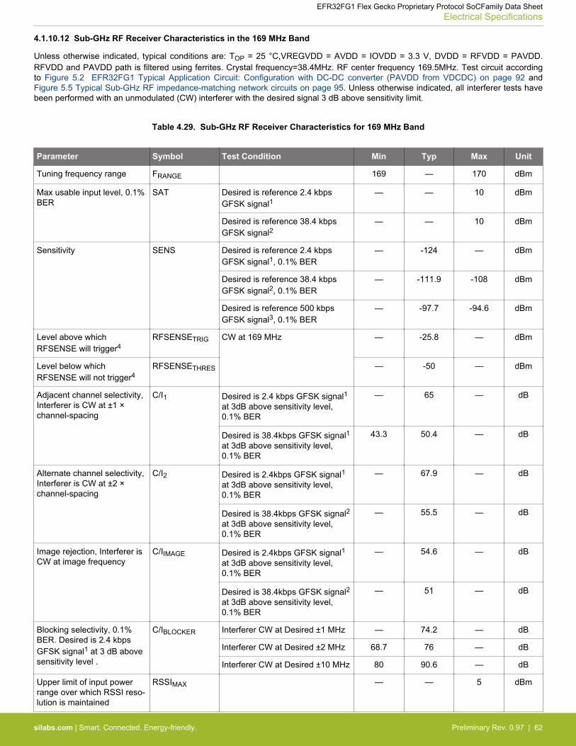
4.1.10.12 Sub-GHz RF Receiver Characteristics in the 169 MHz Band
Unless otherwise indicated, typical conditions are: TOP = 25 °C,VREGVDD = AVDD = IOVDD = 3.3 V, DVDD = RFVDD = PAVDD.RFVDD and PAVDD path is filtered using ferrites. Crystal frequency=38.4MHz. RF center frequency 169.5MHz. Test circuit accordingto Figure 5.2 EFR32FG1 Typical Application Circuit: Configuration with DC-DC converter (PAVDD from VDCDC) on page 92 andFigure 5.5 Typical Sub-GHz RF impedance-matching network circuits on page 95. Unless otherwise indicated, all interferer tests havebeen performed with an unmodulated (CW) interferer with the desired signal 3 dB above sensitivity limit.
Table 4.29. Sub-GHz RF Receiver Characteristics for 169 MHz Band
Parameter Symbol Test Condition Min Typ Max Unit
Tuning frequency range FRANGE 169 — 170 dBm
Max usable input level, 0.1%BER
SAT Desired is reference 2.4 kbpsGFSK signal1
— — 10 dBm
Desired is reference 38.4 kbpsGFSK signal2
— — 10 dBm
Sensitivity SENS Desired is reference 2.4 kbpsGFSK signal1, 0.1% BER
— -124 — dBm
Desired is reference 38.4 kbpsGFSK signal2, 0.1% BER
— -111.9 -108 dBm
Desired is reference 500 kbpsGFSK signal3, 0.1% BER
— -97.7 -94.6 dBm
Level above whichRFSENSE will trigger4
RFSENSETRIG CW at 169 MHz — -25.8 — dBm
Level below whichRFSENSE will not trigger4
RFSENSETHRES — -50 — dBm
Adjacent channel selectivity,Interferer is CW at ±1 ×channel-spacing
C/I1 Desired is 2.4 kbps GFSK signal1at 3dB above sensitivity level,0.1% BER
— 65 — dB
Desired is 38.4kbps GFSK signal1at 3dB above sensitivity level,0.1% BER
43.3 50.4 — dB
Alternate channel selectivity,Interferer is CW at ±2 ×channel-spacing
C/I2 Desired is 2.4kbps GFSK signal1at 3dB above sensitivity level,0.1% BER
— 67.9 — dB
Desired is 38.4kbps GFSK signal2at 3dB above sensitivity level,0.1% BER
— 55.5 — dB
Image rejection, Interferer isCW at image frequency
C/IIMAGE Desired is 2.4kbps GFSK signal1at 3dB above sensitivity level,0.1% BER
— 54.6 — dB
Desired is 38.4kbps GFSK signal2at 3dB above sensitivity level,0.1% BER
— 51 — dB
Blocking selectivity, 0.1%BER. Desired is 2.4 kbpsGFSK signal1 at 3 dB abovesensitivity level .
C/IBLOCKER Interferer CW at Desired ±1 MHz — 74.2 — dB
Interferer CW at Desired ±2 MHz 68.7 76 — dB
Interferer CW at Desired ±10 MHz 80 90.6 — dB
Upper limit of input powerrange over which RSSI reso-lution is maintained
RSSIMAX — — 5 dBm
EFR32FG1 Flex Gecko Proprietary Protocol SoCFamily Data SheetElectrical Specifications
silabs.com | Smart. Connected. Energy-friendly. Preliminary Rev. 0.97 | 62
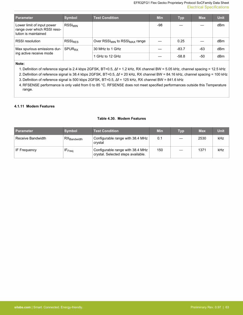
Parameter Symbol Test Condition Min Typ Max Unit
Lower limit of input powerrange over which RSSI reso-lution is maintained
RSSIMIN -98 — — dBm
RSSI resolution RSSIRES Over RSSIMIN to RSSIMAX range — 0.25 — dBm
Max spurious emissions dur-ing active receive mode
SPURRX 30 MHz to 1 GHz — -83.7 -63 dBm
1 GHz to 12 GHz — -58.8 -50 dBm
Note:1. Definition of reference signal is 2.4 kbps 2GFSK, BT=0.5, Δf = 1.2 kHz, RX channel BW = 5.05 kHz, channel spacing = 12.5 kHz2. Definition of reference signal is 38.4 kbps 2GFSK, BT=0.5, Δf = 20 kHz, RX channel BW = 84.16 kHz, channel spacing = 100 kHz3. Definition of reference signal is 500 kbps 2GFSK, BT=0.5, Δf = 125 kHz, RX channel BW = 841.6 kHz4. RFSENSE performance is only valid from 0 to 85 °C. RFSENSE does not meet specified performances outside this Temperature
range.
4.1.11 Modem Features
Table 4.30. Modem Features
Parameter Symbol Test Condition Min Typ Max Unit
Receive Bandwidth RXBandwidth Configurable range with 38.4 MHzcrystal
0.1 — 2530 kHz
IF Frequency IFFreq Configurable range with 38.4 MHzcrystal. Selected steps available.
150 — 1371 kHz
EFR32FG1 Flex Gecko Proprietary Protocol SoCFamily Data SheetElectrical Specifications
silabs.com | Smart. Connected. Energy-friendly. Preliminary Rev. 0.97 | 63
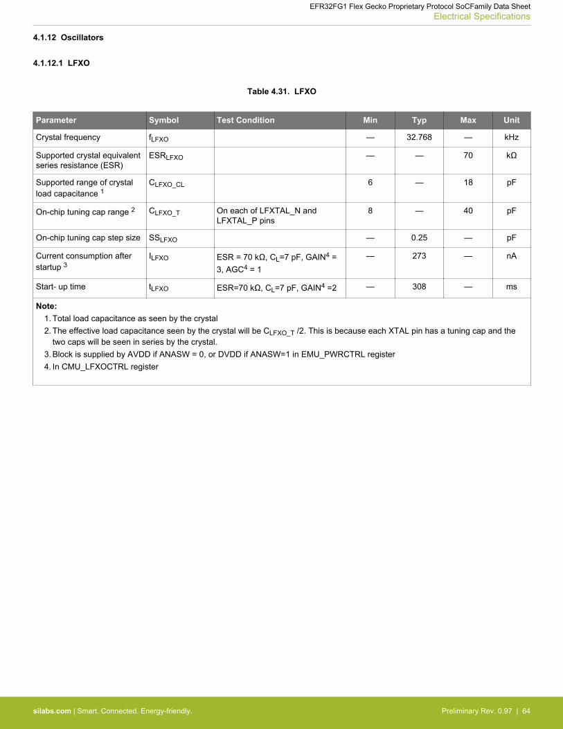
4.1.12 Oscillators
4.1.12.1 LFXO
Table 4.31. LFXO
Parameter Symbol Test Condition Min Typ Max Unit
Crystal frequency fLFXO — 32.768 — kHz
Supported crystal equivalentseries resistance (ESR)
ESRLFXO — — 70 kΩ
Supported range of crystalload capacitance 1
CLFXO_CL 6 — 18 pF
On-chip tuning cap range 2 CLFXO_T On each of LFXTAL_N andLFXTAL_P pins
8 — 40 pF
On-chip tuning cap step size SSLFXO — 0.25 — pF
Current consumption afterstartup 3
ILFXO ESR = 70 kΩ, CL=7 pF, GAIN4 =3, AGC4 = 1
— 273 — nA
Start- up time tLFXO ESR=70 kΩ, CL=7 pF, GAIN4 =2 — 308 — ms
Note:1. Total load capacitance as seen by the crystal2. The effective load capacitance seen by the crystal will be CLFXO_T /2. This is because each XTAL pin has a tuning cap and the
two caps will be seen in series by the crystal.3. Block is supplied by AVDD if ANASW = 0, or DVDD if ANASW=1 in EMU_PWRCTRL register4. In CMU_LFXOCTRL register
EFR32FG1 Flex Gecko Proprietary Protocol SoCFamily Data SheetElectrical Specifications
silabs.com | Smart. Connected. Energy-friendly. Preliminary Rev. 0.97 | 64
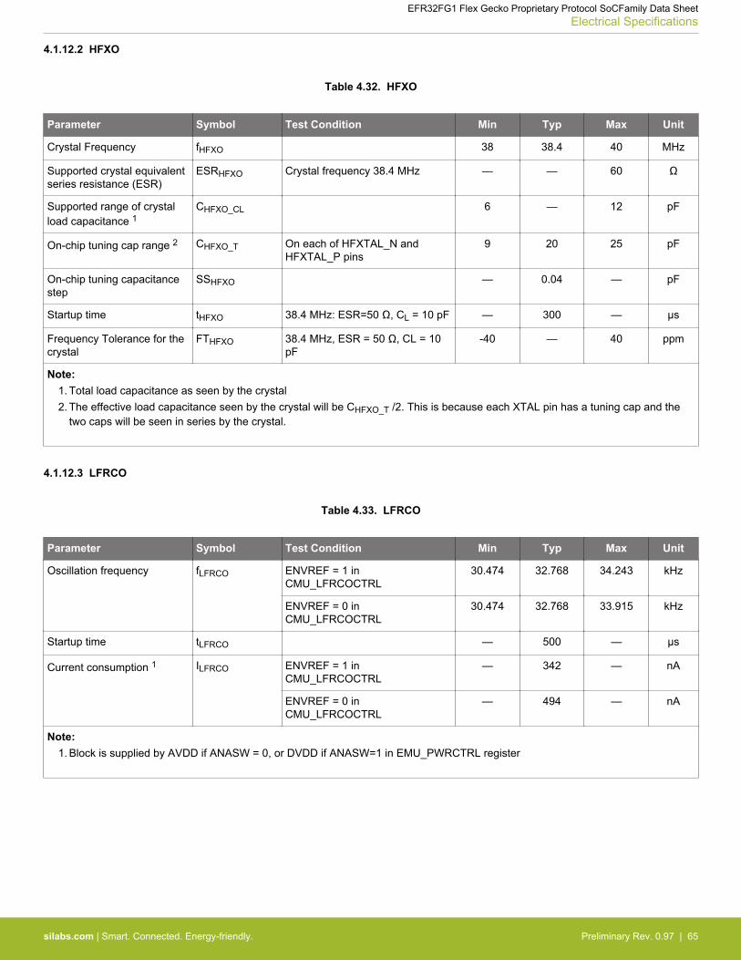
4.1.12.2 HFXO
Table 4.32. HFXO
Parameter Symbol Test Condition Min Typ Max Unit
Crystal Frequency fHFXO 38 38.4 40 MHz
Supported crystal equivalentseries resistance (ESR)
ESRHFXO Crystal frequency 38.4 MHz — — 60 Ω
Supported range of crystalload capacitance 1
CHFXO_CL 6 — 12 pF
On-chip tuning cap range 2 CHFXO_T On each of HFXTAL_N andHFXTAL_P pins
9 20 25 pF
On-chip tuning capacitancestep
SSHFXO — 0.04 — pF
Startup time tHFXO 38.4 MHz: ESR=50 Ω, CL = 10 pF — 300 — μs
Frequency Tolerance for thecrystal
FTHFXO 38.4 MHz, ESR = 50 Ω, CL = 10pF
-40 — 40 ppm
Note:1. Total load capacitance as seen by the crystal2. The effective load capacitance seen by the crystal will be CHFXO_T /2. This is because each XTAL pin has a tuning cap and the
two caps will be seen in series by the crystal.
4.1.12.3 LFRCO
Table 4.33. LFRCO
Parameter Symbol Test Condition Min Typ Max Unit
Oscillation frequency fLFRCO ENVREF = 1 inCMU_LFRCOCTRL
30.474 32.768 34.243 kHz
ENVREF = 0 inCMU_LFRCOCTRL
30.474 32.768 33.915 kHz
Startup time tLFRCO — 500 — μs
Current consumption 1 ILFRCO ENVREF = 1 inCMU_LFRCOCTRL
— 342 — nA
ENVREF = 0 inCMU_LFRCOCTRL
— 494 — nA
Note:1. Block is supplied by AVDD if ANASW = 0, or DVDD if ANASW=1 in EMU_PWRCTRL register
EFR32FG1 Flex Gecko Proprietary Protocol SoCFamily Data SheetElectrical Specifications
silabs.com | Smart. Connected. Energy-friendly. Preliminary Rev. 0.97 | 65
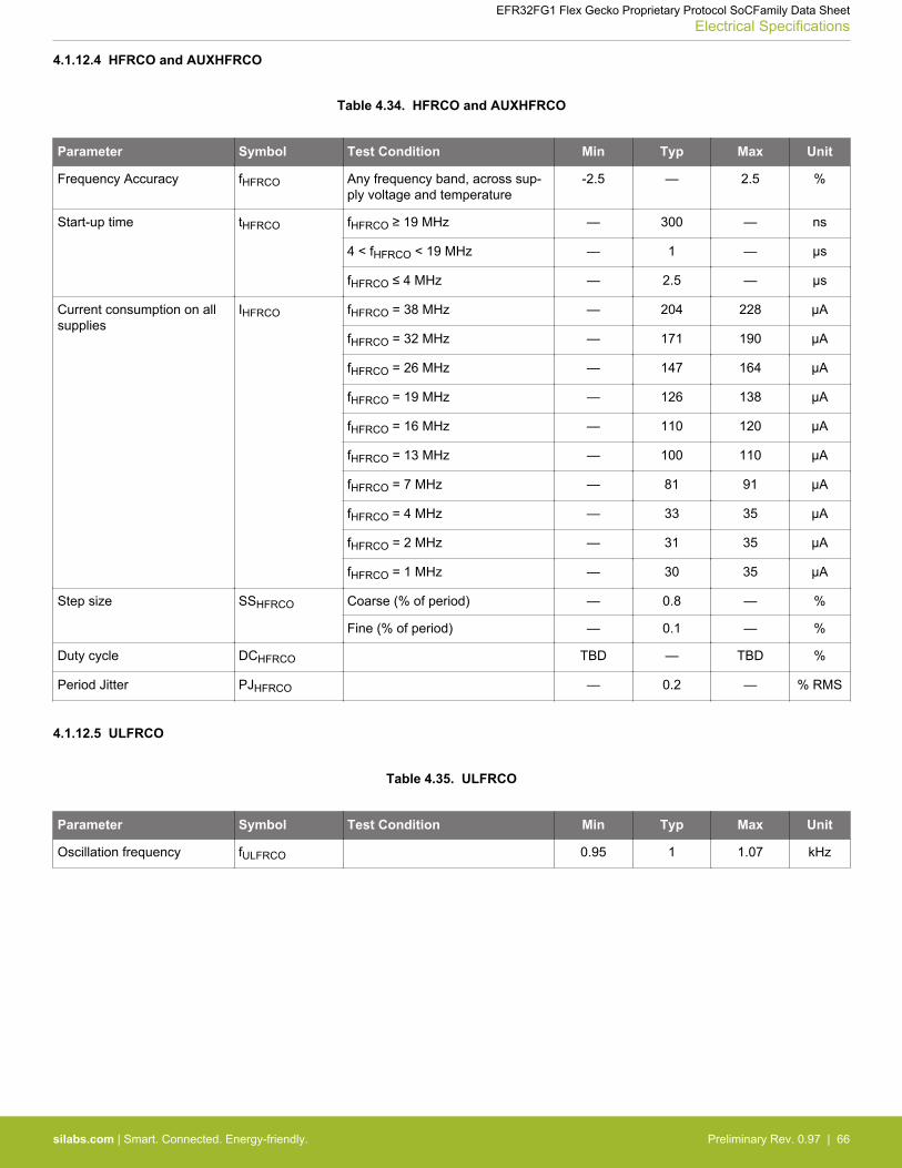
4.1.12.4 HFRCO and AUXHFRCO
Table 4.34. HFRCO and AUXHFRCO
Parameter Symbol Test Condition Min Typ Max Unit
Frequency Accuracy fHFRCO Any frequency band, across sup-ply voltage and temperature
-2.5 — 2.5 %
Start-up time tHFRCO fHFRCO ≥ 19 MHz — 300 — ns
4 < fHFRCO < 19 MHz — 1 — μs
fHFRCO ≤ 4 MHz — 2.5 — μs
Current consumption on allsupplies
IHFRCO fHFRCO = 38 MHz — 204 228 μA
fHFRCO = 32 MHz — 171 190 μA
fHFRCO = 26 MHz — 147 164 μA
fHFRCO = 19 MHz — 126 138 μA
fHFRCO = 16 MHz — 110 120 μA
fHFRCO = 13 MHz — 100 110 μA
fHFRCO = 7 MHz — 81 91 μA
fHFRCO = 4 MHz — 33 35 μA
fHFRCO = 2 MHz — 31 35 μA
fHFRCO = 1 MHz — 30 35 μA
Step size SSHFRCO Coarse (% of period) — 0.8 — %
Fine (% of period) — 0.1 — %
Duty cycle DCHFRCO TBD — TBD %
Period Jitter PJHFRCO — 0.2 — % RMS
4.1.12.5 ULFRCO
Table 4.35. ULFRCO
Parameter Symbol Test Condition Min Typ Max Unit
Oscillation frequency fULFRCO 0.95 1 1.07 kHz
EFR32FG1 Flex Gecko Proprietary Protocol SoCFamily Data SheetElectrical Specifications
silabs.com | Smart. Connected. Energy-friendly. Preliminary Rev. 0.97 | 66
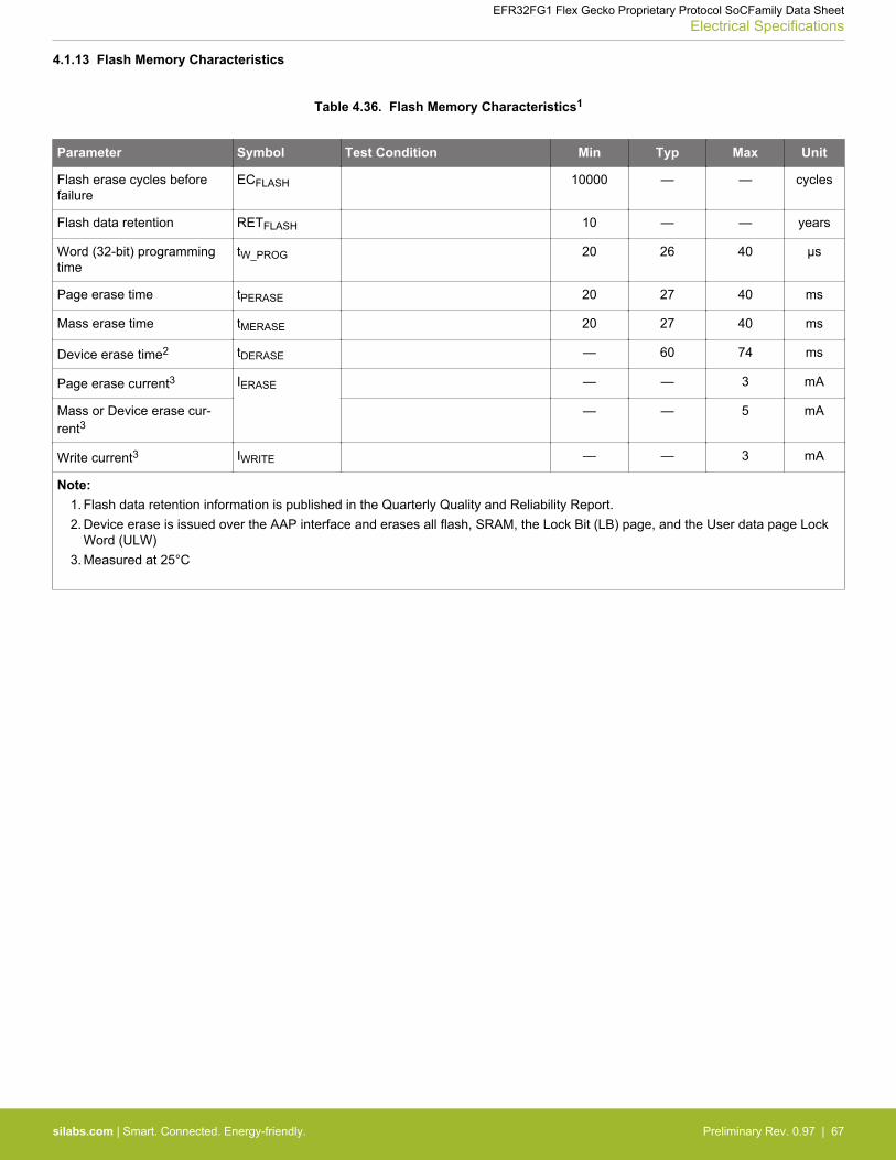
4.1.13 Flash Memory Characteristics
Table 4.36. Flash Memory Characteristics1
Parameter Symbol Test Condition Min Typ Max Unit
Flash erase cycles beforefailure
ECFLASH 10000 — — cycles
Flash data retention RETFLASH 10 — — years
Word (32-bit) programmingtime
tW_PROG 20 26 40 μs
Page erase time tPERASE 20 27 40 ms
Mass erase time tMERASE 20 27 40 ms
Device erase time2 tDERASE — 60 74 ms
Page erase current3 IERASE — — 3 mA
Mass or Device erase cur-rent3
— — 5 mA
Write current3 IWRITE — — 3 mA
Note:1. Flash data retention information is published in the Quarterly Quality and Reliability Report.2. Device erase is issued over the AAP interface and erases all flash, SRAM, the Lock Bit (LB) page, and the User data page Lock
Word (ULW)3. Measured at 25°C
EFR32FG1 Flex Gecko Proprietary Protocol SoCFamily Data SheetElectrical Specifications
silabs.com | Smart. Connected. Energy-friendly. Preliminary Rev. 0.97 | 67
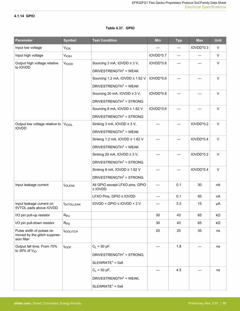
4.1.14 GPIO
Table 4.37. GPIO
Parameter Symbol Test Condition Min Typ Max Unit
Input low voltage VIOIL — — IOVDD*0.3 V
Input high voltage VIOIH IOVDD*0.7 — — V
Output high voltage relativeto IOVDD
VIOOH Sourcing 3 mA, IOVDD ≥ 3 V,
DRIVESTRENGTH1 = WEAK
IOVDD*0.8 — — V
Sourcing 1.2 mA, IOVDD ≥ 1.62 V
DRIVESTRENGTH1 = WEAK
IOVDD*0.6 — — V
Sourcing 20 mA, IOVDD ≥ 3 V,
DRIVESTRENGTH1 = STRONG
IOVDD*0.8 — — V
Sourcing 8 mA, IOVDD ≥ 1.62 V
DRIVESTRENGTH1 = STRONG
IOVDD*0.6 — — V
Output low voltage relative toIOVDD
VIOOL Sinking 3 mA, IOVDD ≥ 3 V,
DRIVESTRENGTH1 = WEAK
— — IOVDD*0.2 V
Sinking 1.2 mA, IOVDD ≥ 1.62 V
DRIVESTRENGTH1 = WEAK
— — IOVDD*0.4 V
Sinking 20 mA, IOVDD ≥ 3 V,
DRIVESTRENGTH1 = STRONG
— — IOVDD*0.2 V
Sinking 8 mA, IOVDD ≥ 1.62 V
DRIVESTRENGTH1 = STRONG
— — IOVDD*0.4 V
Input leakage current IIOLEAK All GPIO except LFXO pins, GPIO≤ IOVDD
— 0.1 30 nA
LFXO Pins, GPIO ≤ IOVDD — 0.1 50 nA
Input leakage current on5VTOL pads above IOVDD
I5VTOLLEAK IOVDD < GPIO ≤ IOVDD + 2 V — 3.3 15 μA
I/O pin pull-up resistor RPU 30 43 65 kΩ
I/O pin pull-down resistor RPD 30 43 65 kΩ
Pulse width of pulses re-moved by the glitch suppres-sion filter
tIOGLITCH 20 25 35 ns
Output fall time, From 70%to 30% of VIO
tIOOF CL = 50 pF,
DRIVESTRENGTH1 = STRONG,
SLEWRATE1 = 0x6
— 1.8 — ns
CL = 50 pF,
DRIVESTRENGTH1 = WEAK,
SLEWRATE1 = 0x6
— 4.5 — ns
EFR32FG1 Flex Gecko Proprietary Protocol SoCFamily Data SheetElectrical Specifications
silabs.com | Smart. Connected. Energy-friendly. Preliminary Rev. 0.97 | 68
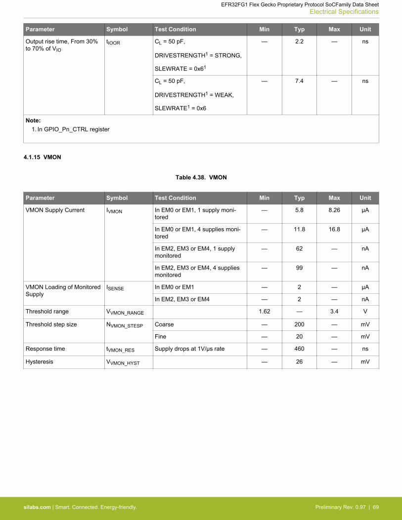
Parameter Symbol Test Condition Min Typ Max Unit
Output rise time, From 30%to 70% of VIO
tIOOR CL = 50 pF,
DRIVESTRENGTH1 = STRONG,
SLEWRATE = 0x61
— 2.2 — ns
CL = 50 pF,
DRIVESTRENGTH1 = WEAK,
SLEWRATE1 = 0x6
— 7.4 — ns
Note:1. In GPIO_Pn_CTRL register
4.1.15 VMON
Table 4.38. VMON
Parameter Symbol Test Condition Min Typ Max Unit
VMON Supply Current IVMON In EM0 or EM1, 1 supply moni-tored
— 5.8 8.26 μA
In EM0 or EM1, 4 supplies moni-tored
— 11.8 16.8 μA
In EM2, EM3 or EM4, 1 supplymonitored
— 62 — nA
In EM2, EM3 or EM4, 4 suppliesmonitored
— 99 — nA
VMON Loading of MonitoredSupply
ISENSE In EM0 or EM1 — 2 — μA
In EM2, EM3 or EM4 — 2 — nA
Threshold range VVMON_RANGE 1.62 — 3.4 V
Threshold step size NVMON_STESP Coarse — 200 — mV
Fine — 20 — mV
Response time tVMON_RES Supply drops at 1V/μs rate — 460 — ns
Hysteresis VVMON_HYST — 26 — mV
EFR32FG1 Flex Gecko Proprietary Protocol SoCFamily Data SheetElectrical Specifications
silabs.com | Smart. Connected. Energy-friendly. Preliminary Rev. 0.97 | 69
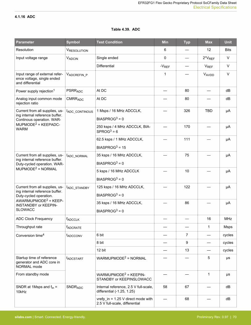
4.1.16 ADC
Table 4.39. ADC
Parameter Symbol Test Condition Min Typ Max Unit
Resolution VRESOLUTION 6 — 12 Bits
Input voltage range VADCIN Single ended 0 — 2*VREF V
Differential -VREF — VREF V
Input range of external refer-ence voltage, single endedand differential
VADCREFIN_P 1 — VAVDD V
Power supply rejection1 PSRRADC At DC — 80 — dB
Analog input common moderejection ratio
CMRRADC At DC — 80 — dB
Current from all supplies, us-ing internal reference buffer.Continous operation. WAR-MUPMODE2 = KEEPADC-WARM
IADC_CONTINOUS 1 Msps / 16 MHz ADCCLK,
BIASPROG3 = 0
— 326 TBD μA
250 ksps / 4 MHz ADCCLK, BIA-SPROG3 = 6
— 170 — μA
62.5 ksps / 1 MHz ADCCLK,
BIASPROG3 = 15
— 111 — μA
Current from all supplies, us-ing internal reference buffer.Duty-cycled operation. WAR-MUPMODE2 = NORMAL
IADC_NORMAL 35 ksps / 16 MHz ADCCLK,
BIASPROG3 = 0
— 75 — μA
5 ksps / 16 MHz ADCCLK
BIASPROG3 = 0
— 10 — μA
Current from all supplies, us-ing internal reference buffer.Duty-cycled operation.AWARMUPMODE2 = KEEP-INSTANDBY or KEEPIN-SLOWACC
IADC_STANDBY 125 ksps / 16 MHz ADCCLK,
BIASPROG3 = 0
— 122 — μA
35 ksps / 16 MHz ADCCLK,
BIASPROG3 = 0
— 86 — μA
ADC Clock Frequency fADCCLK — — 16 MHz
Throughput rate fADCRATE — — 1 Msps
Conversion time4 tADCCONV 6 bit — 7 — cycles
8 bit — 9 — cycles
12 bit — 13 — cycles
Startup time of referencegenerator and ADC core inNORMAL mode
tADCSTART WARMUPMODE2 = NORMAL — — 5 μs
From standby mode WARMUPMODE2 = KEEPIN-STANDBY or KEEPINSLOWACC
— — 1 μs
SNDR at 1Msps and fin =10kHz
SNDRADC Internal reference, 2.5 V full-scale,differential (-1.25, 1.25)
58 67 — dB
vrefp_in = 1.25 V direct mode with2.5 V full-scale, differential
— 68 — dB
EFR32FG1 Flex Gecko Proprietary Protocol SoCFamily Data SheetElectrical Specifications
silabs.com | Smart. Connected. Energy-friendly. Preliminary Rev. 0.97 | 70
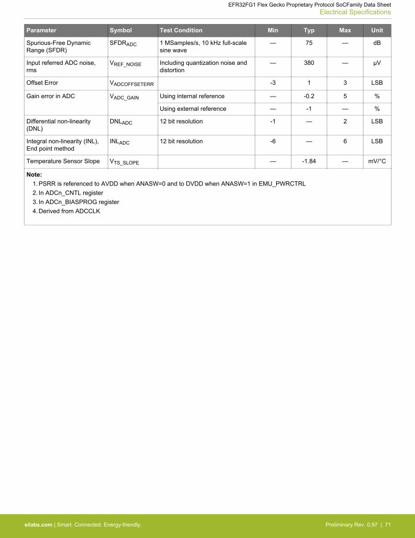
Parameter Symbol Test Condition Min Typ Max Unit
Spurious-Free DynamicRange (SFDR)
SFDRADC 1 MSamples/s, 10 kHz full-scalesine wave
— 75 — dB
Input referred ADC noise,rms
VREF_NOISE Including quantization noise anddistortion
— 380 — μV
Offset Error VADCOFFSETERR -3 1 3 LSB
Gain error in ADC VADC_GAIN Using internal reference — -0.2 5 %
Using external reference — -1 — %
Differential non-linearity(DNL)
DNLADC 12 bit resolution -1 — 2 LSB
Integral non-linearity (INL),End point method
INLADC 12 bit resolution -6 — 6 LSB
Temperature Sensor Slope VTS_SLOPE — -1.84 — mV/°C
Note:1. PSRR is referenced to AVDD when ANASW=0 and to DVDD when ANASW=1 in EMU_PWRCTRL2. In ADCn_CNTL register3. In ADCn_BIASPROG register4. Derived from ADCCLK
EFR32FG1 Flex Gecko Proprietary Protocol SoCFamily Data SheetElectrical Specifications
silabs.com | Smart. Connected. Energy-friendly. Preliminary Rev. 0.97 | 71
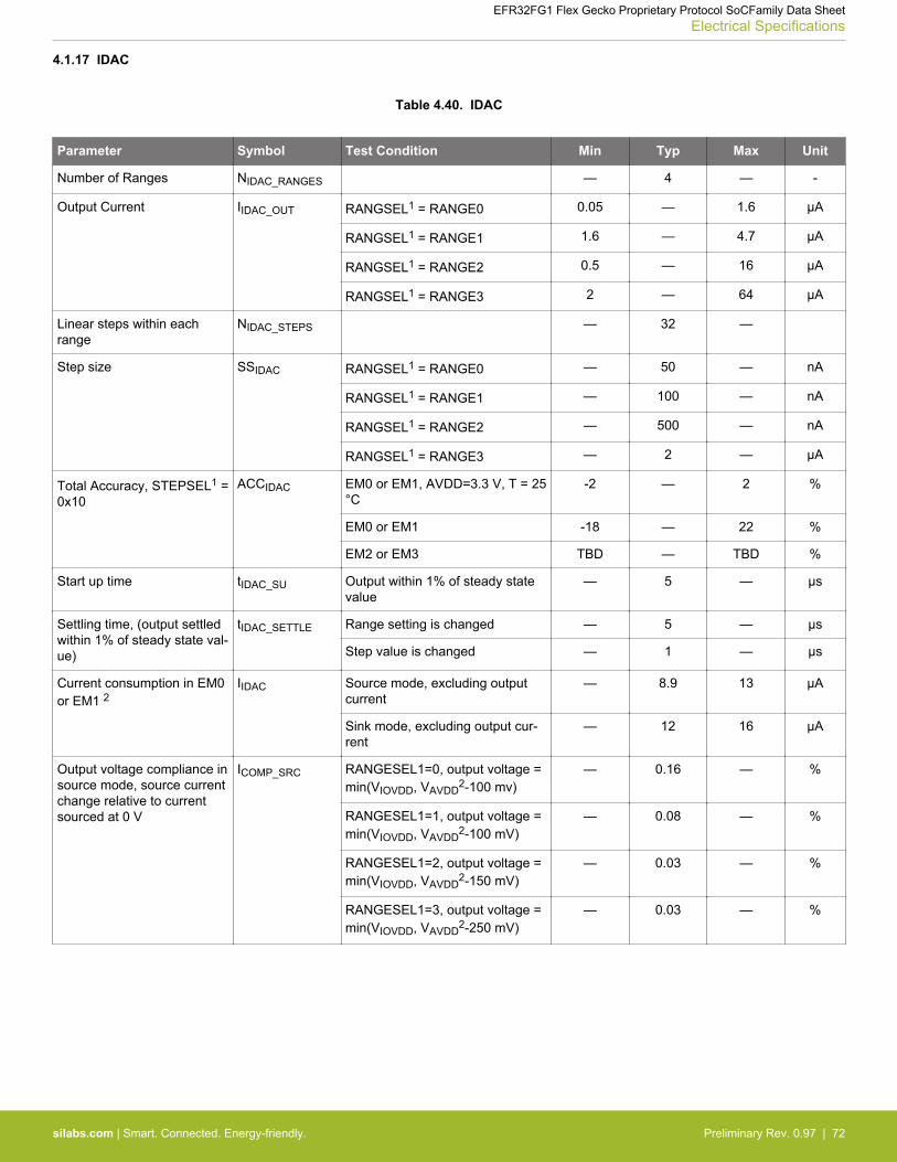
4.1.17 IDAC
Table 4.40. IDAC
Parameter Symbol Test Condition Min Typ Max Unit
Number of Ranges NIDAC_RANGES — 4 — -
Output Current IIDAC_OUT RANGSEL1 = RANGE0 0.05 — 1.6 μA
RANGSEL1 = RANGE1 1.6 — 4.7 μA
RANGSEL1 = RANGE2 0.5 — 16 μA
RANGSEL1 = RANGE3 2 — 64 μA
Linear steps within eachrange
NIDAC_STEPS — 32 —
Step size SSIDAC RANGSEL1 = RANGE0 — 50 — nA
RANGSEL1 = RANGE1 — 100 — nA
RANGSEL1 = RANGE2 — 500 — nA
RANGSEL1 = RANGE3 — 2 — μA
Total Accuracy, STEPSEL1 =0x10
ACCIDAC EM0 or EM1, AVDD=3.3 V, T = 25°C
-2 — 2 %
EM0 or EM1 -18 — 22 %
EM2 or EM3 TBD — TBD %
Start up time tIDAC_SU Output within 1% of steady statevalue
— 5 — μs
Settling time, (output settledwithin 1% of steady state val-ue)
tIDAC_SETTLE Range setting is changed — 5 — μs
Step value is changed — 1 — μs
Current consumption in EM0or EM1 2
IIDAC Source mode, excluding outputcurrent
— 8.9 13 μA
Sink mode, excluding output cur-rent
— 12 16 μA
Output voltage compliance insource mode, source currentchange relative to currentsourced at 0 V
ICOMP_SRC RANGESEL1=0, output voltage =min(VIOVDD, VAVDD
2-100 mv)— 0.16 — %
RANGESEL1=1, output voltage =min(VIOVDD, VAVDD
2-100 mV)— 0.08 — %
RANGESEL1=2, output voltage =min(VIOVDD, VAVDD
2-150 mV)— 0.03 — %
RANGESEL1=3, output voltage =min(VIOVDD, VAVDD
2-250 mV)— 0.03 — %
EFR32FG1 Flex Gecko Proprietary Protocol SoCFamily Data SheetElectrical Specifications
silabs.com | Smart. Connected. Energy-friendly. Preliminary Rev. 0.97 | 72
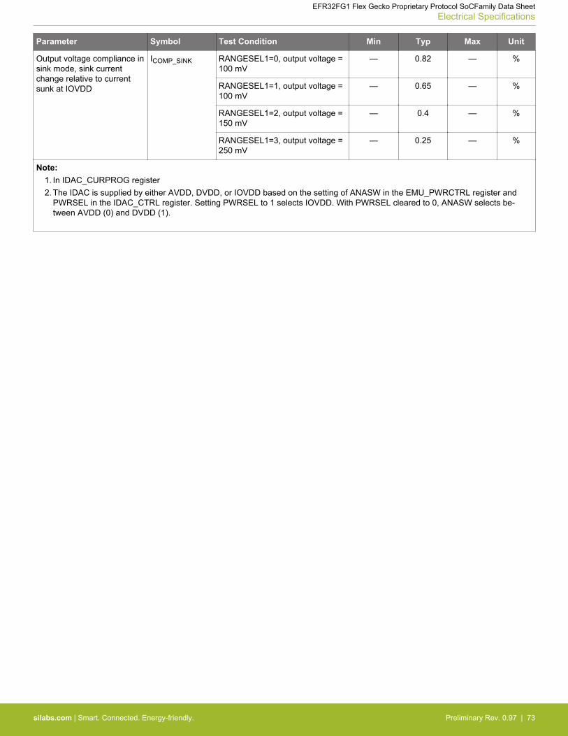
Parameter Symbol Test Condition Min Typ Max Unit
Output voltage compliance insink mode, sink currentchange relative to currentsunk at IOVDD
ICOMP_SINK RANGESEL1=0, output voltage =100 mV
— 0.82 — %
RANGESEL1=1, output voltage =100 mV
— 0.65 — %
RANGESEL1=2, output voltage =150 mV
— 0.4 — %
RANGESEL1=3, output voltage =250 mV
— 0.25 — %
Note:1. In IDAC_CURPROG register2. The IDAC is supplied by either AVDD, DVDD, or IOVDD based on the setting of ANASW in the EMU_PWRCTRL register and
PWRSEL in the IDAC_CTRL register. Setting PWRSEL to 1 selects IOVDD. With PWRSEL cleared to 0, ANASW selects be-tween AVDD (0) and DVDD (1).
EFR32FG1 Flex Gecko Proprietary Protocol SoCFamily Data SheetElectrical Specifications
silabs.com | Smart. Connected. Energy-friendly. Preliminary Rev. 0.97 | 73
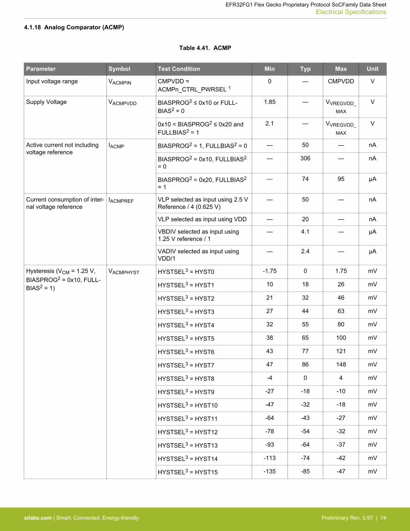
4.1.18 Analog Comparator (ACMP)
Table 4.41. ACMP
Parameter Symbol Test Condition Min Typ Max Unit
Input voltage range VACMPIN CMPVDD =ACMPn_CTRL_PWRSEL 1
0 — CMPVDD V
Supply Voltage VACMPVDD BIASPROG2 ≤ 0x10 or FULL-BIAS2 = 0
1.85 — VVREGVDD_
MAX
V
0x10 < BIASPROG2 ≤ 0x20 andFULLBIAS2 = 1
2.1 — VVREGVDD_
MAX
V
Active current not includingvoltage reference
IACMP BIASPROG2 = 1, FULLBIAS2 = 0 — 50 — nA
BIASPROG2 = 0x10, FULLBIAS2
= 0— 306 — nA
BIASPROG2 = 0x20, FULLBIAS2
= 1— 74 95 μA
Current consumption of inter-nal voltage reference
IACMPREF VLP selected as input using 2.5 VReference / 4 (0.625 V)
— 50 — nA
VLP selected as input using VDD — 20 — nA
VBDIV selected as input using1.25 V reference / 1
— 4.1 — μA
VADIV selected as input usingVDD/1
— 2.4 — μA
Hysteresis (VCM = 1.25 V,BIASPROG2 = 0x10, FULL-BIAS2 = 1)
VACMPHYST HYSTSEL3 = HYST0 -1.75 0 1.75 mV
HYSTSEL3 = HYST1 10 18 26 mV
HYSTSEL3 = HYST2 21 32 46 mV
HYSTSEL3 = HYST3 27 44 63 mV
HYSTSEL3 = HYST4 32 55 80 mV
HYSTSEL3 = HYST5 38 65 100 mV
HYSTSEL3 = HYST6 43 77 121 mV
HYSTSEL3 = HYST7 47 86 148 mV
HYSTSEL3 = HYST8 -4 0 4 mV
HYSTSEL3 = HYST9 -27 -18 -10 mV
HYSTSEL3 = HYST10 -47 -32 -18 mV
HYSTSEL3 = HYST11 -64 -43 -27 mV
HYSTSEL3 = HYST12 -78 -54 -32 mV
HYSTSEL3 = HYST13 -93 -64 -37 mV
HYSTSEL3 = HYST14 -113 -74 -42 mV
HYSTSEL3 = HYST15 -135 -85 -47 mV
EFR32FG1 Flex Gecko Proprietary Protocol SoCFamily Data SheetElectrical Specifications
silabs.com | Smart. Connected. Energy-friendly. Preliminary Rev. 0.97 | 74
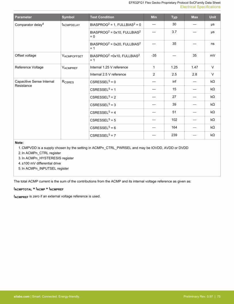
Parameter Symbol Test Condition Min Typ Max Unit
Comparator delay4 tACMPDELAY BIASPROG2 = 1, FULLBIAS2 = 0 — 30 — μs
BIASPROG2 = 0x10, FULLBIAS2
= 0— 3.7 — μs
BIASPROG2 = 0x20, FULLBIAS2
= 1— 35 — ns
Offset voltage VACMPOFFSET BIASPROG2 =0x10, FULLBIAS2
= 1-35 — 35 mV
Reference Voltage VACMPREF Internal 1.25 V reference 1 1.25 1.47 V
Internal 2.5 V reference 2 2.5 2.8 V
Capacitive Sense InternalResistance
RCSRES CSRESSEL5 = 0 — inf — kΩ
CSRESSEL5 = 1 — 15 — kΩ
CSRESSEL5 = 2 — 27 — kΩ
CSRESSEL5 = 3 — 39 — kΩ
CSRESSEL5 = 4 — 51 — kΩ
CSRESSEL5 = 5 — 102 — kΩ
CSRESSEL5 = 6 — 164 — kΩ
CSRESSEL5 = 7 — 239 — kΩ
Note:1. CMPVDD is a supply chosen by the setting in ACMPn_CTRL_PWRSEL and may be IOVDD, AVDD or DVDD2. In ACMPn_CTRL register3. In ACMPn_HYSTERESIS register4. ±100 mV differential drive5. In ACMPn_INPUTSEL register
The total ACMP current is the sum of the contributions from the ACMP and its internal voltage reference as given as:
IACMPTOTAL = IACMP + IACMPREF
IACMPREF is zero if an external voltage reference is used.
EFR32FG1 Flex Gecko Proprietary Protocol SoCFamily Data SheetElectrical Specifications
silabs.com | Smart. Connected. Energy-friendly. Preliminary Rev. 0.97 | 75
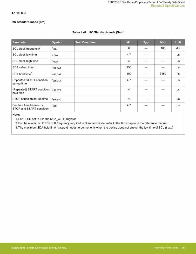
4.1.19 I2C
I2C Standard-mode (Sm)
Table 4.42. I2C Standard-mode (Sm)1
Parameter Symbol Test Condition Min Typ Max Unit
SCL clock frequency2 fSCL 0 — 100 kHz
SCL clock low time tLOW 4.7 — — μs
SCL clock high time tHIGH 4 — — μs
SDA set-up time tSU,DAT 250 — — ns
SDA hold time3 tHD,DAT 100 — 3450 ns
Repeated START conditionset-up time
tSU,STA 4.7 — — μs
(Repeated) START conditionhold time
tHD,STA 4 — — μs
STOP condition set-up time tSU,STO 4 — — μs
Bus free time between aSTOP and START condition
tBUF 4.7 — — μs
Note:1. For CLHR set to 0 in the I2Cn_CTRL register2. For the minimum HFPERCLK frequency required in Standard-mode, refer to the I2C chapter in the reference manual3. The maximum SDA hold time (tHD,DAT) needs to be met only when the device does not stretch the low time of SCL (tLOW)
EFR32FG1 Flex Gecko Proprietary Protocol SoCFamily Data SheetElectrical Specifications
silabs.com | Smart. Connected. Energy-friendly. Preliminary Rev. 0.97 | 76
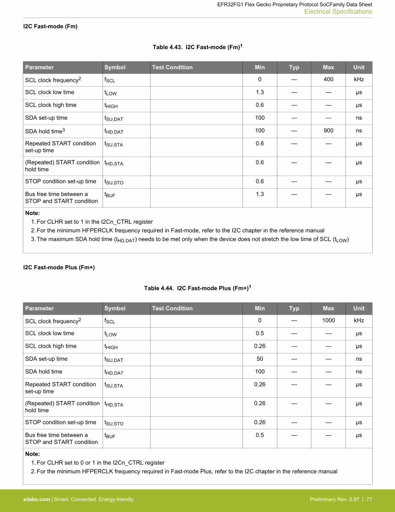
I2C Fast-mode (Fm)
Table 4.43. I2C Fast-mode (Fm)1
Parameter Symbol Test Condition Min Typ Max Unit
SCL clock frequency2 fSCL 0 — 400 kHz
SCL clock low time tLOW 1.3 — — μs
SCL clock high time tHIGH 0.6 — — μs
SDA set-up time tSU,DAT 100 — — ns
SDA hold time3 tHD,DAT 100 — 900 ns
Repeated START conditionset-up time
tSU,STA 0.6 — — μs
(Repeated) START conditionhold time
tHD,STA 0.6 — — μs
STOP condition set-up time tSU,STO 0.6 — — μs
Bus free time between aSTOP and START condition
tBUF 1.3 — — μs
Note:1. For CLHR set to 1 in the I2Cn_CTRL register2. For the minimum HFPERCLK frequency required in Fast-mode, refer to the I2C chapter in the reference manual3. The maximum SDA hold time (tHD,DAT) needs to be met only when the device does not stretch the low time of SCL (tLOW)
I2C Fast-mode Plus (Fm+)
Table 4.44. I2C Fast-mode Plus (Fm+)1
Parameter Symbol Test Condition Min Typ Max Unit
SCL clock frequency2 fSCL 0 — 1000 kHz
SCL clock low time tLOW 0.5 — — μs
SCL clock high time tHIGH 0.26 — — μs
SDA set-up time tSU,DAT 50 — — ns
SDA hold time tHD,DAT 100 — — ns
Repeated START conditionset-up time
tSU,STA 0.26 — — μs
(Repeated) START conditionhold time
tHD,STA 0.26 — — μs
STOP condition set-up time tSU,STO 0.26 — — μs
Bus free time between aSTOP and START condition
tBUF 0.5 — — μs
Note:1. For CLHR set to 0 or 1 in the I2Cn_CTRL register2. For the minimum HFPERCLK frequency required in Fast-mode Plus, refer to the I2C chapter in the reference manual
EFR32FG1 Flex Gecko Proprietary Protocol SoCFamily Data SheetElectrical Specifications
silabs.com | Smart. Connected. Energy-friendly. Preliminary Rev. 0.97 | 77
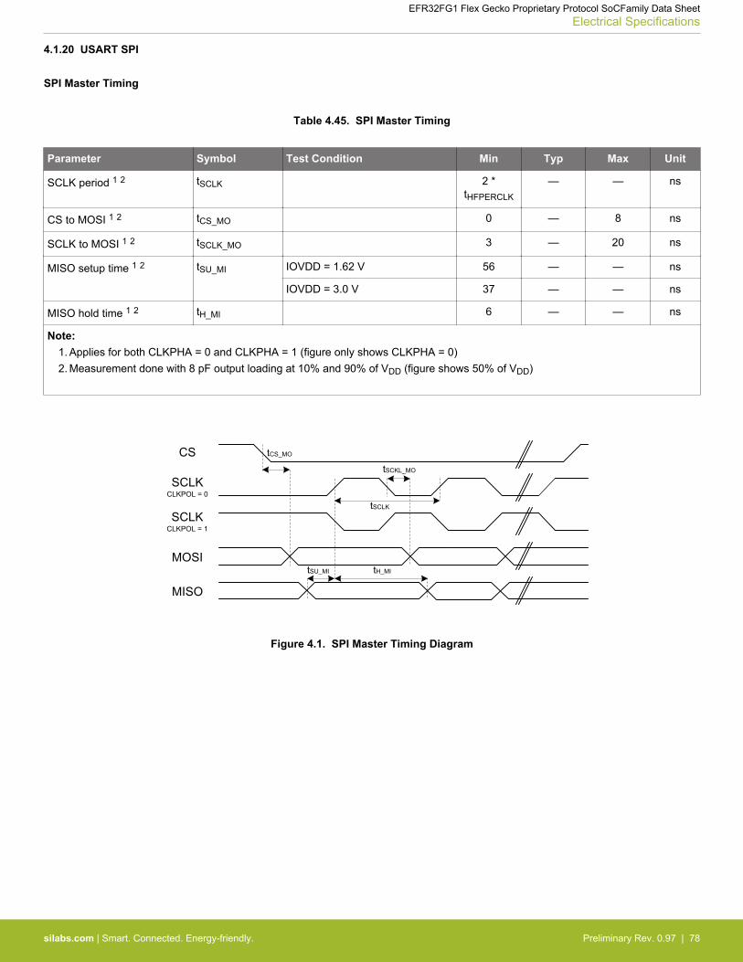
4.1.20 USART SPI
SPI Master Timing
Table 4.45. SPI Master Timing
Parameter Symbol Test Condition Min Typ Max Unit
SCLK period 1 2 tSCLK 2 *tHFPERCLK
— — ns
CS to MOSI 1 2 tCS_MO 0 — 8 ns
SCLK to MOSI 1 2 tSCLK_MO 3 — 20 ns
MISO setup time 1 2 tSU_MI IOVDD = 1.62 V 56 — — ns
IOVDD = 3.0 V 37 — — ns
MISO hold time 1 2 tH_MI 6 — — ns
Note:1. Applies for both CLKPHA = 0 and CLKPHA = 1 (figure only shows CLKPHA = 0)2. Measurement done with 8 pF output loading at 10% and 90% of VDD (figure shows 50% of VDD)
CS
SCLKCLKPOL = 0
MOSI
MISO
tCS_MO
tH_MItSU_MI
tSCKL_MO
tSCLK
SCLKCLKPOL = 1
Figure 4.1. SPI Master Timing Diagram
EFR32FG1 Flex Gecko Proprietary Protocol SoCFamily Data SheetElectrical Specifications
silabs.com | Smart. Connected. Energy-friendly. Preliminary Rev. 0.97 | 78
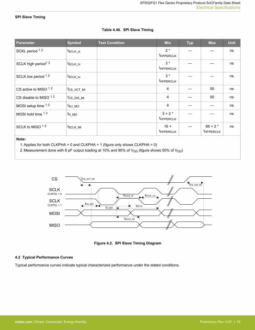
SPI Slave Timing
Table 4.46. SPI Slave Timing
Parameter Symbol Test Condition Min Typ Max Unit
SCKL period 1 2 tSCLK_sl 2 *tHFPERCLK
— — ns
SCLK high period1 2 tSCLK_hi 3 *tHFPERCLK
— — ns
SCLK low period 1 2 tSCLK_lo 3 *tHFPERCLK
— — ns
CS active to MISO 1 2 tCS_ACT_MI 4 — 50 ns
CS disable to MISO 1 2 tCS_DIS_MI 4 — 50 ns
MOSI setup time 1 2 tSU_MO 4 — — ns
MOSI hold time 1 2 tH_MO 3 + 2 *tHFPERCLK
— — ns
SCLK to MISO 1 2 tSCLK_MI 16 +tHFPERCLK
— 66 + 2 *tHFPERCLK
ns
Note:1. Applies for both CLKPHA = 0 and CLKPHA = 1 (figure only shows CLKPHA = 0)2. Measurement done with 8 pF output loading at 10% and 90% of VDD (figure shows 50% of VDD)
CS
SCLKCLKPOL = 0
MOSI
MISO
tCS_ACT_MI
tSCLK_HI
tSCLKtSU_MO
tH_MO
tSCLK_MI
tCS_DIS_MI
tSCLK_LO
SCLKCLKPOL = 1
Figure 4.2. SPI Slave Timing Diagram
4.2 Typical Performance Curves
Typical performance curves indicate typical characterized performance under the stated conditions.
EFR32FG1 Flex Gecko Proprietary Protocol SoCFamily Data SheetElectrical Specifications
silabs.com | Smart. Connected. Energy-friendly. Preliminary Rev. 0.97 | 79
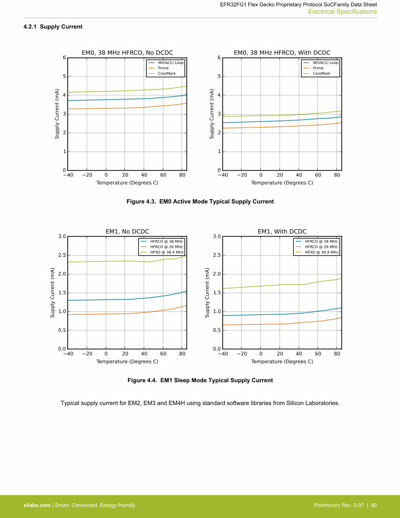
4.2.1 Supply Current
Figure 4.3. EM0 Active Mode Typical Supply Current
Figure 4.4. EM1 Sleep Mode Typical Supply Current
Typical supply current for EM2, EM3 and EM4H using standard software libraries from Silicon Laboratories.
EFR32FG1 Flex Gecko Proprietary Protocol SoCFamily Data SheetElectrical Specifications
silabs.com | Smart. Connected. Energy-friendly. Preliminary Rev. 0.97 | 80
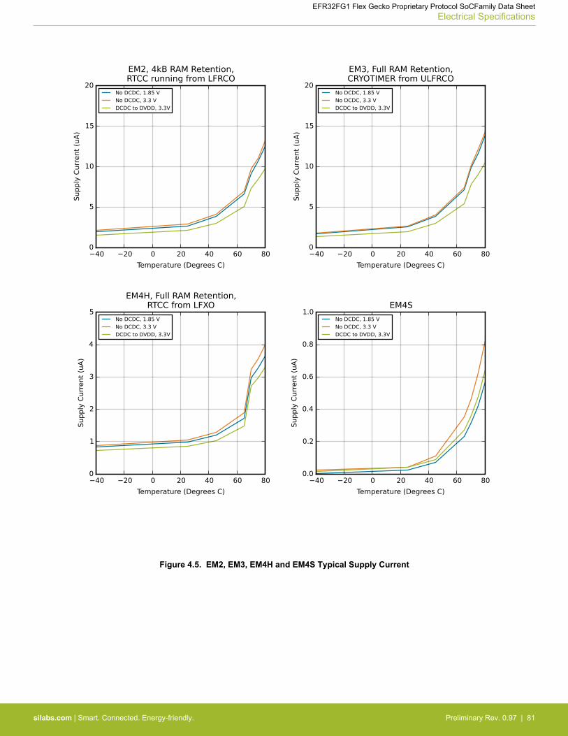
Figure 4.5. EM2, EM3, EM4H and EM4S Typical Supply Current
EFR32FG1 Flex Gecko Proprietary Protocol SoCFamily Data SheetElectrical Specifications
silabs.com | Smart. Connected. Energy-friendly. Preliminary Rev. 0.97 | 81
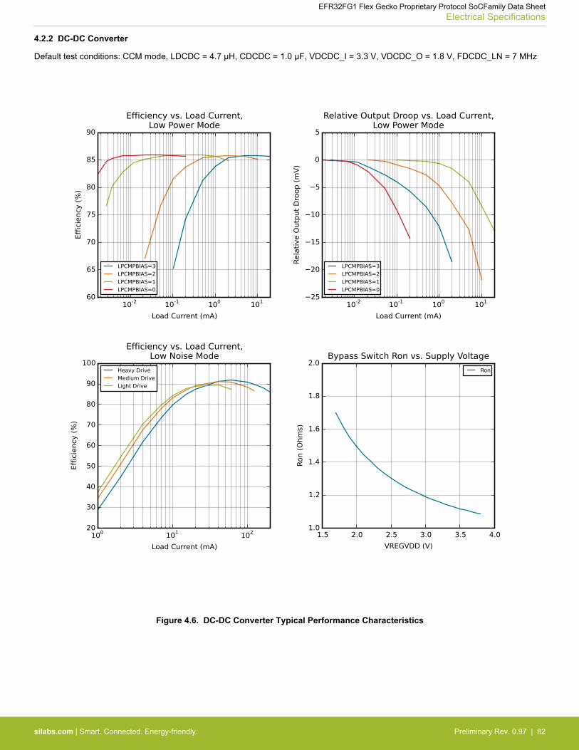
4.2.2 DC-DC Converter
Default test conditions: CCM mode, LDCDC = 4.7 μH, CDCDC = 1.0 μF, VDCDC_I = 3.3 V, VDCDC_O = 1.8 V, FDCDC_LN = 7 MHz
Figure 4.6. DC-DC Converter Typical Performance Characteristics
EFR32FG1 Flex Gecko Proprietary Protocol SoCFamily Data SheetElectrical Specifications
silabs.com | Smart. Connected. Energy-friendly. Preliminary Rev. 0.97 | 82
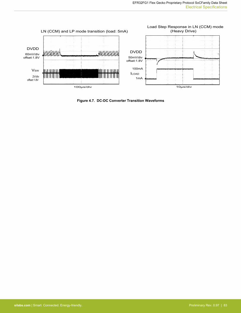
100μs/div 10μs/div
2V/div offset:1.8V
50mV/div offset:1.8V
100mA
1mAILOAD
60mV/div offset:1.8V
VSW
DVDDDVDD
Load Step Response in LN (CCM) mode(Heavy Drive)LN (CCM) and LP mode transition (load: 5mA)
Figure 4.7. DC-DC Converter Transition Waveforms
EFR32FG1 Flex Gecko Proprietary Protocol SoCFamily Data SheetElectrical Specifications
silabs.com | Smart. Connected. Energy-friendly. Preliminary Rev. 0.97 | 83
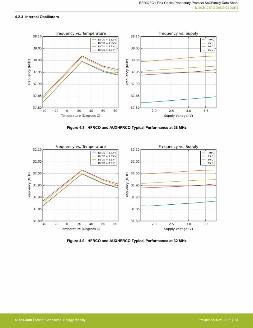
4.2.3 Internal Oscillators
Figure 4.8. HFRCO and AUXHFRCO Typical Performance at 38 MHz
Figure 4.9. HFRCO and AUXHFRCO Typical Performance at 32 MHz
EFR32FG1 Flex Gecko Proprietary Protocol SoCFamily Data SheetElectrical Specifications
silabs.com | Smart. Connected. Energy-friendly. Preliminary Rev. 0.97 | 84
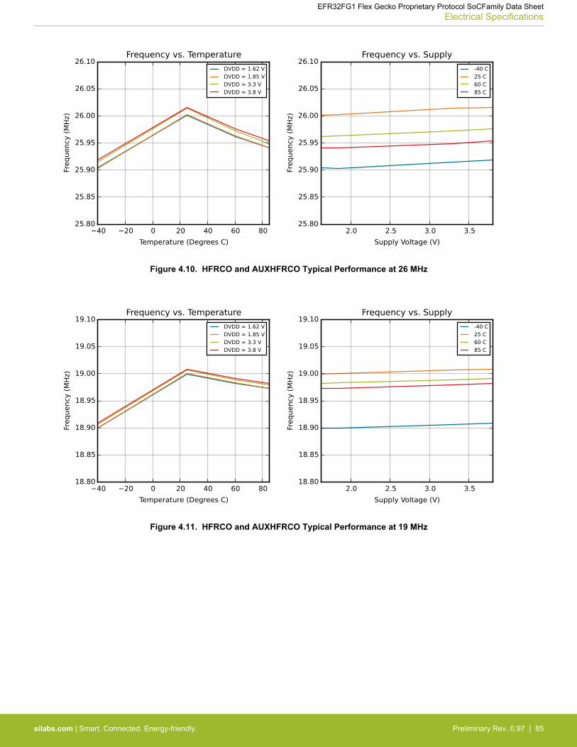
Figure 4.10. HFRCO and AUXHFRCO Typical Performance at 26 MHz
Figure 4.11. HFRCO and AUXHFRCO Typical Performance at 19 MHz
EFR32FG1 Flex Gecko Proprietary Protocol SoCFamily Data SheetElectrical Specifications
silabs.com | Smart. Connected. Energy-friendly. Preliminary Rev. 0.97 | 85
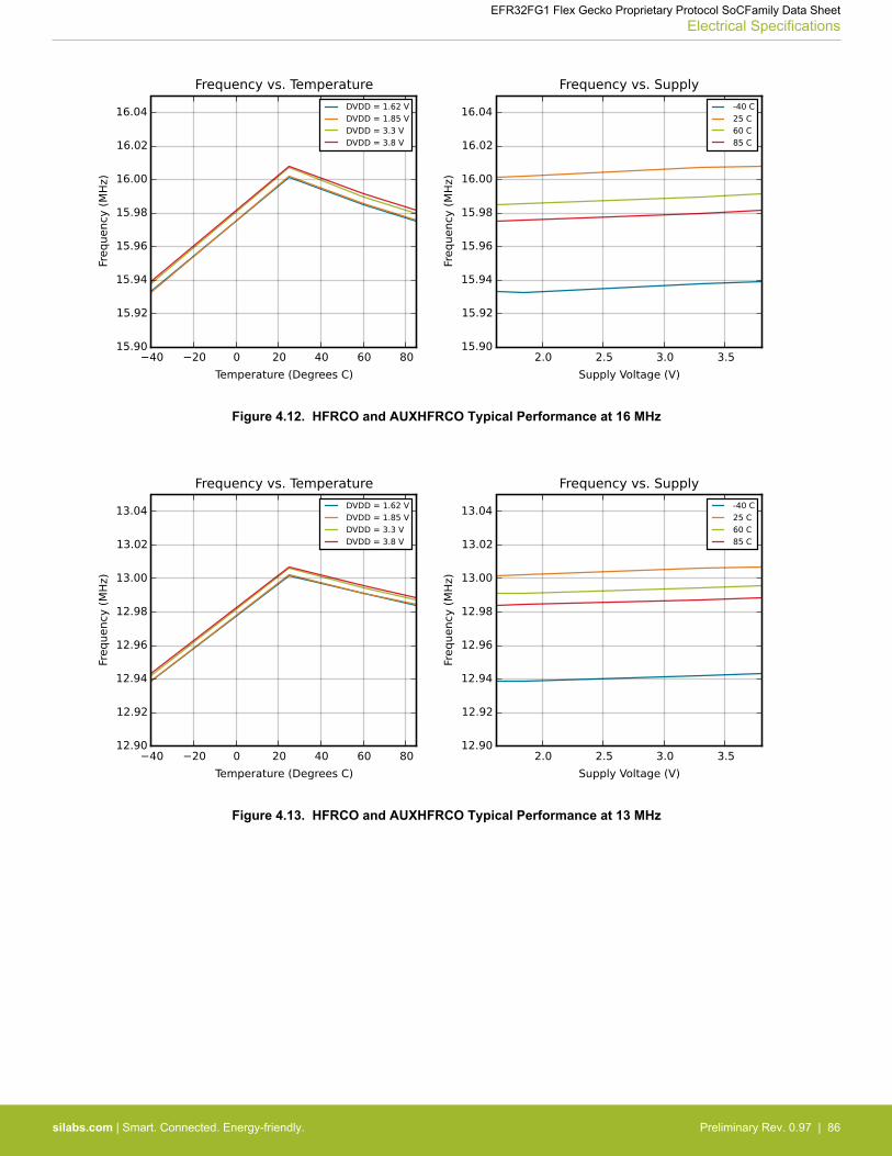
Figure 4.12. HFRCO and AUXHFRCO Typical Performance at 16 MHz
Figure 4.13. HFRCO and AUXHFRCO Typical Performance at 13 MHz
EFR32FG1 Flex Gecko Proprietary Protocol SoCFamily Data SheetElectrical Specifications
silabs.com | Smart. Connected. Energy-friendly. Preliminary Rev. 0.97 | 86
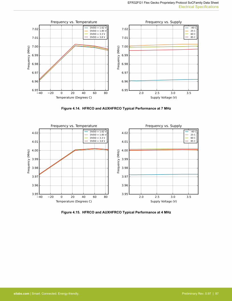
Figure 4.14. HFRCO and AUXHFRCO Typical Performance at 7 MHz
Figure 4.15. HFRCO and AUXHFRCO Typical Performance at 4 MHz
EFR32FG1 Flex Gecko Proprietary Protocol SoCFamily Data SheetElectrical Specifications
silabs.com | Smart. Connected. Energy-friendly. Preliminary Rev. 0.97 | 87
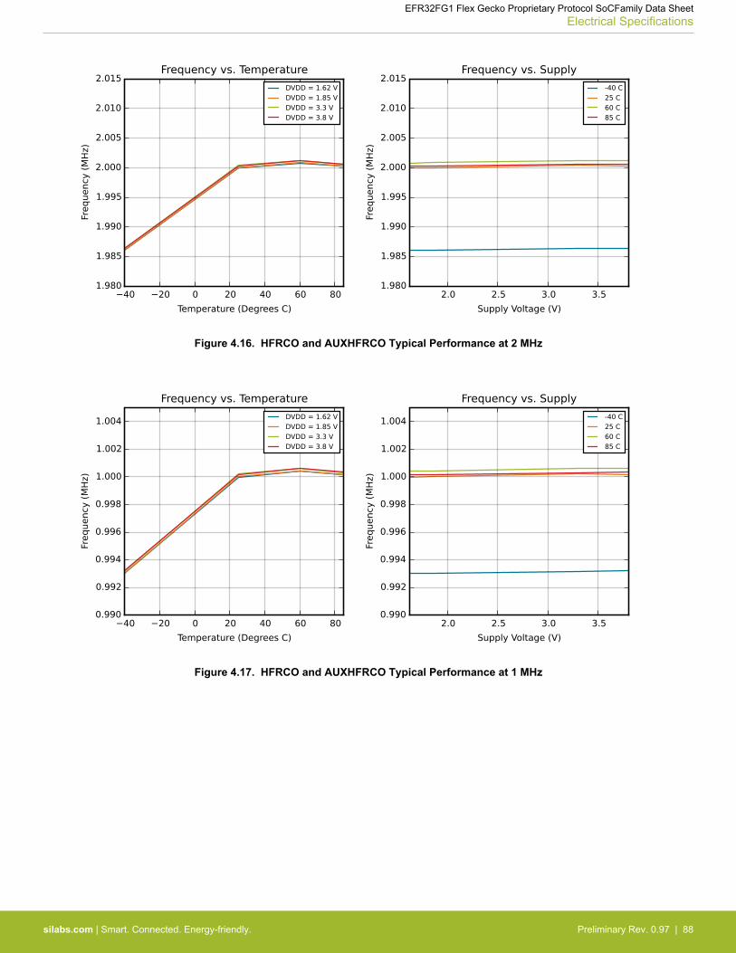
Figure 4.16. HFRCO and AUXHFRCO Typical Performance at 2 MHz
Figure 4.17. HFRCO and AUXHFRCO Typical Performance at 1 MHz
EFR32FG1 Flex Gecko Proprietary Protocol SoCFamily Data SheetElectrical Specifications
silabs.com | Smart. Connected. Energy-friendly. Preliminary Rev. 0.97 | 88
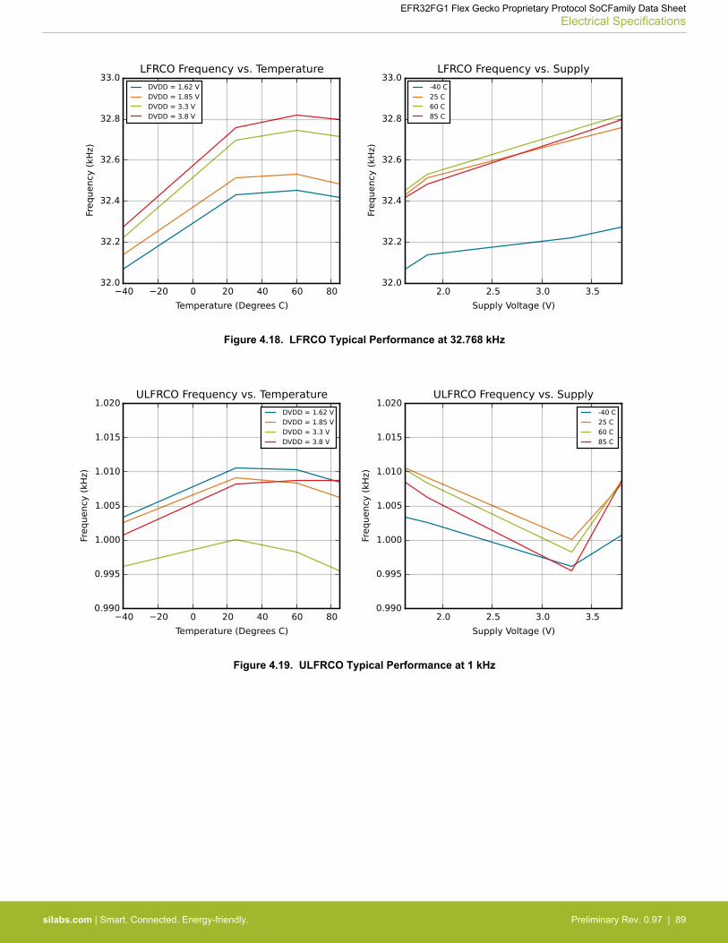
Figure 4.18. LFRCO Typical Performance at 32.768 kHz
Figure 4.19. ULFRCO Typical Performance at 1 kHz
EFR32FG1 Flex Gecko Proprietary Protocol SoCFamily Data SheetElectrical Specifications
silabs.com | Smart. Connected. Energy-friendly. Preliminary Rev. 0.97 | 89
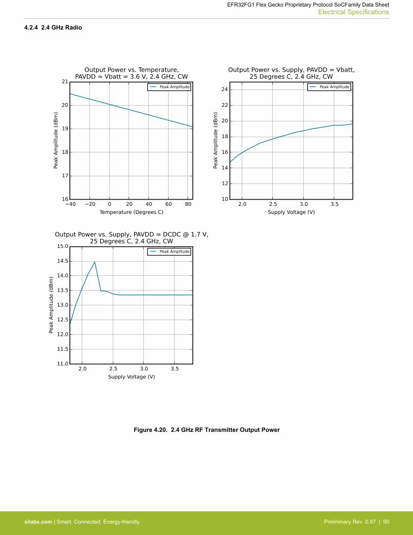
4.2.4 2.4 GHz Radio
Figure 4.20. 2.4 GHz RF Transmitter Output Power
EFR32FG1 Flex Gecko Proprietary Protocol SoCFamily Data SheetElectrical Specifications
silabs.com | Smart. Connected. Energy-friendly. Preliminary Rev. 0.97 | 90
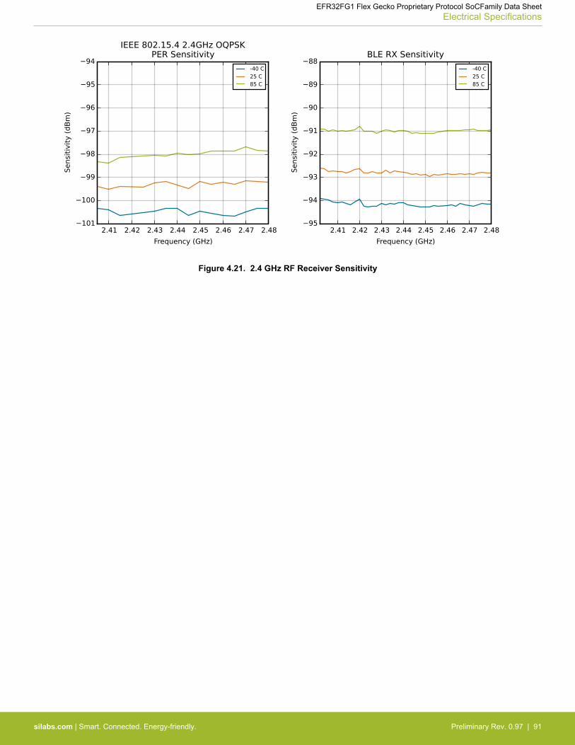
Figure 4.21. 2.4 GHz RF Receiver Sensitivity
EFR32FG1 Flex Gecko Proprietary Protocol SoCFamily Data SheetElectrical Specifications
silabs.com | Smart. Connected. Energy-friendly. Preliminary Rev. 0.97 | 91
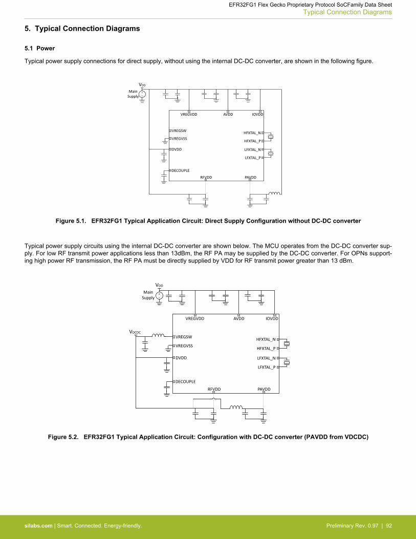
5. Typical Connection Diagrams
5.1 Power
Typical power supply connections for direct supply, without using the internal DC-DC converter, are shown in the following figure.
MainSupply
VDD
VREGVDD AVDD IOVDD
VREGSW
VREGVSS
DVDD
DECOUPLE
RFVDD PAVDD
HFXTAL_N
HFXTAL_P
LFXTAL_N
LFXTAL_P
+–
Figure 5.1. EFR32FG1 Typical Application Circuit: Direct Supply Configuration without DC-DC converter
Typical power supply circuits using the internal DC-DC converter are shown below. The MCU operates from the DC-DC converter sup-ply. For low RF transmit power applications less than 13dBm, the RF PA may be supplied by the DC-DC converter. For OPNs support-ing high power RF transmission, the RF PA must be directly supplied by VDD for RF transmit power greater than 13 dBm.
MainSupply
VDCDC
VDD
VREGVDD AVDD IOVDD
VREGSW
VREGVSS
DVDD
DECOUPLE
RFVDD PAVDD
HFXTAL_N
HFXTAL_P
LFXTAL_N
LFXTAL_P
+–
Figure 5.2. EFR32FG1 Typical Application Circuit: Configuration with DC-DC converter (PAVDD from VDCDC)
EFR32FG1 Flex Gecko Proprietary Protocol SoCFamily Data SheetTypical Connection Diagrams
silabs.com | Smart. Connected. Energy-friendly. Preliminary Rev. 0.97 | 92
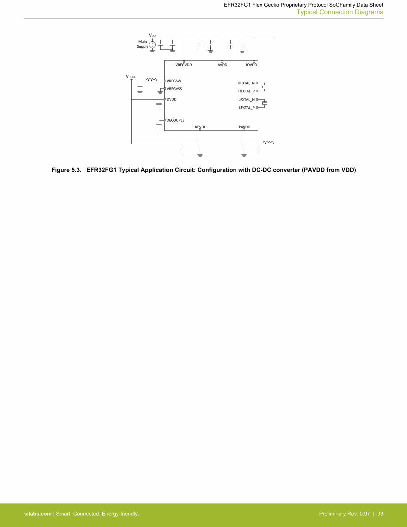
MainSupply
VDCDC
VDD
VREGVDD AVDD IOVDD
VREGSW
VREGVSS
DVDD
DECOUPLE
RFVDD PAVDD
HFXTAL_N
HFXTAL_P
LFXTAL_N
LFXTAL_P
+–
Figure 5.3. EFR32FG1 Typical Application Circuit: Configuration with DC-DC converter (PAVDD from VDD)
EFR32FG1 Flex Gecko Proprietary Protocol SoCFamily Data SheetTypical Connection Diagrams
silabs.com | Smart. Connected. Energy-friendly. Preliminary Rev. 0.97 | 93
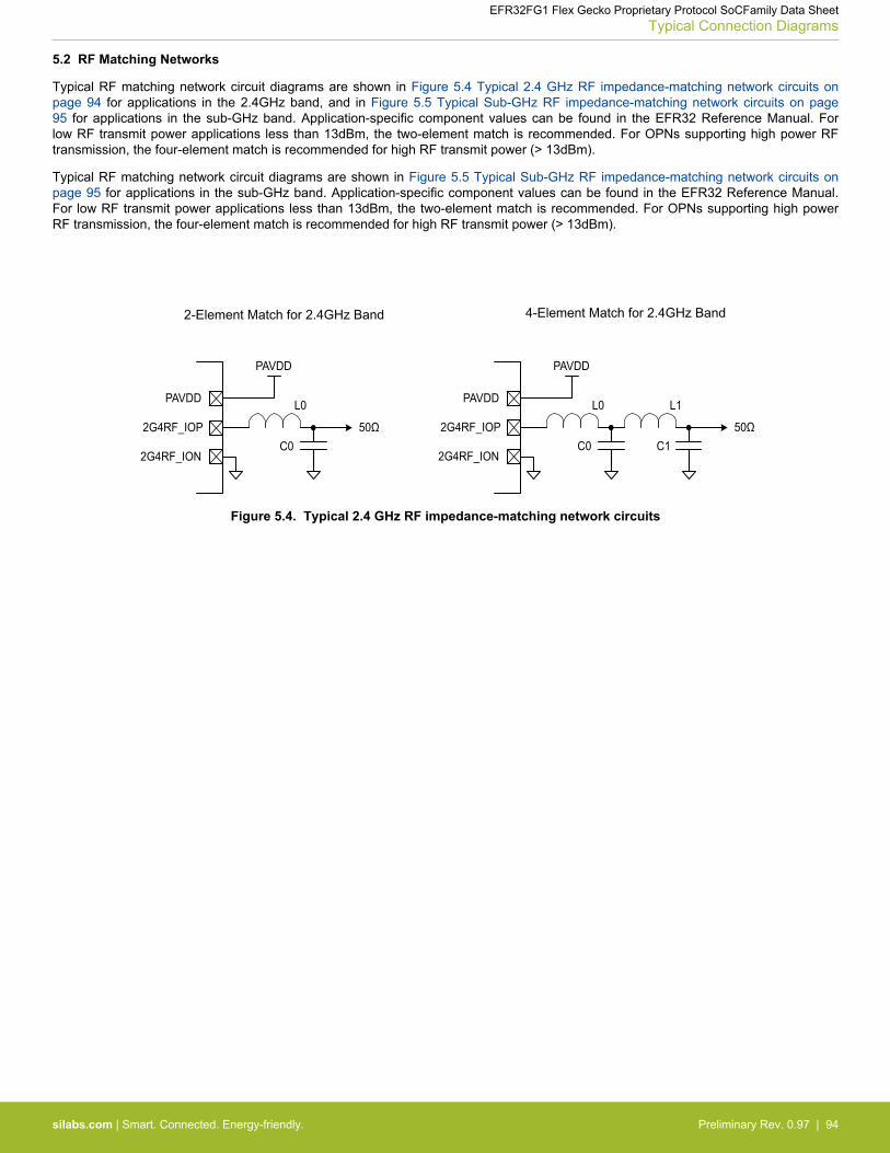
5.2 RF Matching Networks
Typical RF matching network circuit diagrams are shown in Figure 5.4 Typical 2.4 GHz RF impedance-matching network circuits onpage 94 for applications in the 2.4GHz band, and in Figure 5.5 Typical Sub-GHz RF impedance-matching network circuits on page95 for applications in the sub-GHz band. Application-specific component values can be found in the EFR32 Reference Manual. Forlow RF transmit power applications less than 13dBm, the two-element match is recommended. For OPNs supporting high power RFtransmission, the four-element match is recommended for high RF transmit power (> 13dBm).
Typical RF matching network circuit diagrams are shown in Figure 5.5 Typical Sub-GHz RF impedance-matching network circuits onpage 95 for applications in the sub-GHz band. Application-specific component values can be found in the EFR32 Reference Manual.For low RF transmit power applications less than 13dBm, the two-element match is recommended. For OPNs supporting high powerRF transmission, the four-element match is recommended for high RF transmit power (> 13dBm).
2-Element Match for 2.4GHz Band 4-Element Match for 2.4GHz Band
L0
C050Ω2G4RF_IOP
2G4RF_ION 2G4RF_ION
2G4RF_IOP
L0 L1
C0 C150Ω
PAVDD PAVDD
PAVDD PAVDD
Figure 5.4. Typical 2.4 GHz RF impedance-matching network circuits
EFR32FG1 Flex Gecko Proprietary Protocol SoCFamily Data SheetTypical Connection Diagrams
silabs.com | Smart. Connected. Energy-friendly. Preliminary Rev. 0.97 | 94
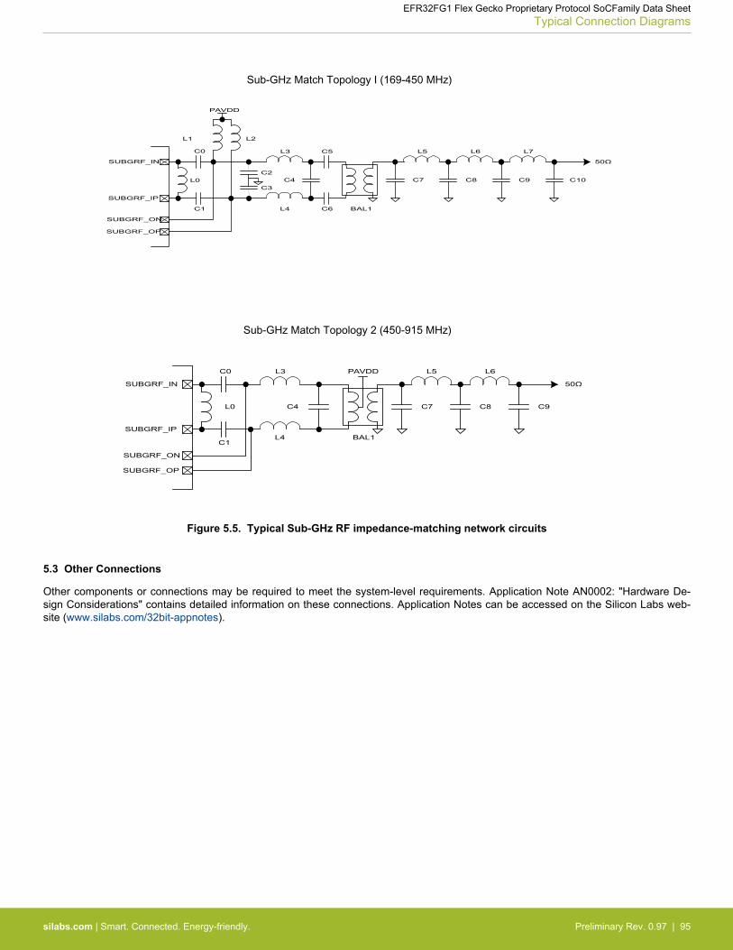
Sub-GHz Match Topology I (169-450 MHz)
Sub-GHz Match Topology 2 (450-915 MHz)
SUBGRF_IN
SUBGRF_IP
SUBGRF_ON
SUBGRF_OP
50Ω
PAVDD
L0
C0
C1
L3
L4
C4 C7
BAL1
C8 C9
L5 L6
SUBGRF_IN
SUBGRF_IP
SUBGRF_ON
SUBGRF_OP
50Ω
PAVDD
L0
C0
C1
L3
L4
C4 C7
BAL1
C8 C9
L5 L6
L1 L2
C2
C3
C5
C6
C10
L7
Figure 5.5. Typical Sub-GHz RF impedance-matching network circuits
5.3 Other Connections
Other components or connections may be required to meet the system-level requirements. Application Note AN0002: "Hardware De-sign Considerations" contains detailed information on these connections. Application Notes can be accessed on the Silicon Labs web-site (www.silabs.com/32bit-appnotes).
EFR32FG1 Flex Gecko Proprietary Protocol SoCFamily Data SheetTypical Connection Diagrams
silabs.com | Smart. Connected. Energy-friendly. Preliminary Rev. 0.97 | 95
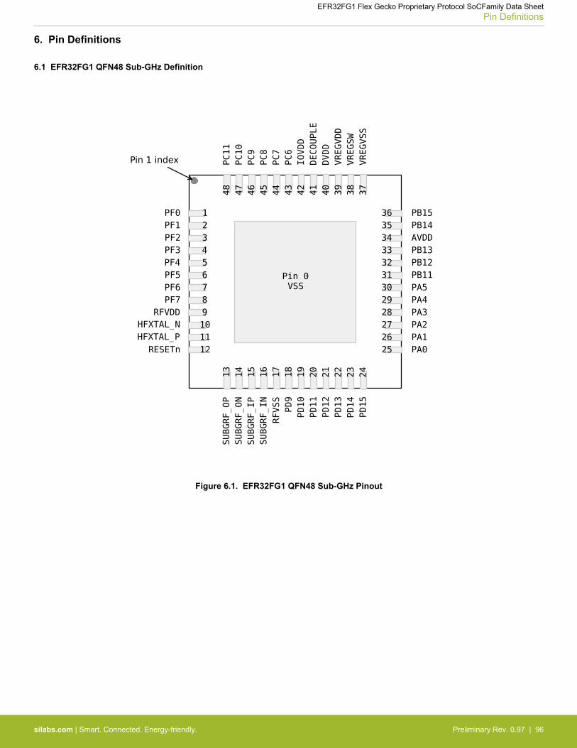
6. Pin Definitions
6.1 EFR32FG1 QFN48 Sub-GHz Definition
Figure 6.1. EFR32FG1 QFN48 Sub-GHz Pinout
EFR32FG1 Flex Gecko Proprietary Protocol SoCFamily Data SheetPin Definitions
silabs.com | Smart. Connected. Energy-friendly. Preliminary Rev. 0.97 | 96

Table 6.1. QFN48 Sub-GHz Device Pinout
QFN48 Pin# andName
Pin Alternate Functionality / Description
Pin# Pin Name Analog Timers Communication Radio Other
0 VSS Ground
1 PF0
BUSAX [ADC0:APORT1XCH16
ACMP0:APORT1XCH16
ACMP1:APORT1XCH16]
BUSBY [ADC0:APORT2YCH16
ACMP0:APORT2YCH16
ACMP1:APORT2YCH16]
TIM0_CC0 #24TIM0_CC1 #23TIM0_CC2 #22
TIM0_CDTI0 #21TIM0_CDTI1 #20TIM0_CDTI2 #19TIM1_CC0 #24TIM1_CC1 #23TIM1_CC2 #22
TIM1_CC3 #21 LE-TIM0_OUT0 #24
LETIM0_OUT1 #23PCNT0_S0IN #24PCNT0_S1IN #23
US0_TX #24US0_RX #23
US0_CLK #22US0_CS #21
US0_CTS #20US0_RTS #19US1_TX #24US1_RX #23
US1_CLK #22US1_CS #21
US1_CTS #20US1_RTS #19LEU0_TX #24LEU0_RX #23I2C0_SDA #24I2C0_SCL #23
FRC_DCLK #24FRC_DOUT #23
FRC_DFRAME #22MODEM_DCLK #24MODEM_DIN #23
MODEM_DOUT #22MODEM_ANT0 #21MODEM_ANT1 #20
PRS_CH0 #0PRS_CH1 #7PRS_CH2 #6PRS_CH3 #5
ACMP0_O #24ACMP1_O #24
DBG_SWCLKTCK#0
2 PF1
BUSAY [ADC0:APORT1YCH17
ACMP0:APORT1YCH17
ACMP1:APORT1YCH17]
BUSBX [ADC0:APORT2XCH17
ACMP0:APORT2XCH17
ACMP1:APORT2XCH17]
TIM0_CC0 #25TIM0_CC1 #24TIM0_CC2 #23
TIM0_CDTI0 #22TIM0_CDTI1 #21TIM0_CDTI2 #20TIM1_CC0 #25TIM1_CC1 #24TIM1_CC2 #23
TIM1_CC3 #22 LE-TIM0_OUT0 #25
LETIM0_OUT1 #24PCNT0_S0IN #25PCNT0_S1IN #24
US0_TX #25US0_RX #24
US0_CLK #23US0_CS #22
US0_CTS #21US0_RTS #20US1_TX #25US1_RX #24
US1_CLK #23US1_CS #22
US1_CTS #21US1_RTS #20LEU0_TX #25LEU0_RX #24I2C0_SDA #25I2C0_SCL #24
FRC_DCLK #25FRC_DOUT #24
FRC_DFRAME #23MODEM_DCLK #25MODEM_DIN #24
MODEM_DOUT #23MODEM_ANT0 #22MODEM_ANT1 #21
PRS_CH0 #1PRS_CH1 #0PRS_CH2 #7PRS_CH3 #6
ACMP0_O #25ACMP1_O #25
DBG_SWDIOTMS#0
3 PF2
BUSAX [ADC0:APORT1XCH18
ACMP0:APORT1XCH18
ACMP1:APORT1XCH18]
BUSBY [ADC0:APORT2YCH18
ACMP0:APORT2YCH18
ACMP1:APORT2YCH18]
TIM0_CC0 #26TIM0_CC1 #25TIM0_CC2 #24
TIM0_CDTI0 #23TIM0_CDTI1 #22TIM0_CDTI2 #21TIM1_CC0 #26TIM1_CC1 #25TIM1_CC2 #24
TIM1_CC3 #23 LE-TIM0_OUT0 #26
LETIM0_OUT1 #25PCNT0_S0IN #26PCNT0_S1IN #25
US0_TX #26US0_RX #25
US0_CLK #24US0_CS #23
US0_CTS #22US0_RTS #21US1_TX #26US1_RX #25
US1_CLK #24US1_CS #23
US1_CTS #22US1_RTS #21LEU0_TX #26LEU0_RX #25I2C0_SDA #26I2C0_SCL #25
FRC_DCLK #26FRC_DOUT #25
FRC_DFRAME #24MODEM_DCLK #26MODEM_DIN #25
MODEM_DOUT #24MODEM_ANT0 #23MODEM_ANT1 #22
CMU_CLK0 #6PRS_CH0 #2PRS_CH1 #1PRS_CH2 #0PRS_CH3 #7
ACMP0_O #26ACMP1_O #26DBG_TDO #0DBG_SWO #0
GPIO_EM4WU0
EFR32FG1 Flex Gecko Proprietary Protocol SoCFamily Data SheetPin Definitions
silabs.com | Smart. Connected. Energy-friendly. Preliminary Rev. 0.97 | 97
QFN48 Pin# andName
Pin Alternate Functionality / Description
Pin# Pin Name Analog Timers Communication Radio Other
4 PF3
BUSAY [ADC0:APORT1YCH19
ACMP0:APORT1YCH19
ACMP1:APORT1YCH19]
BUSBX [ADC0:APORT2XCH19
ACMP0:APORT2XCH19
ACMP1:APORT2XCH19]
TIM0_CC0 #27TIM0_CC1 #26TIM0_CC2 #25
TIM0_CDTI0 #24TIM0_CDTI1 #23TIM0_CDTI2 #22TIM1_CC0 #27TIM1_CC1 #26TIM1_CC2 #25
TIM1_CC3 #24 LE-TIM0_OUT0 #27
LETIM0_OUT1 #26PCNT0_S0IN #27PCNT0_S1IN #26
US0_TX #27US0_RX #26
US0_CLK #25US0_CS #24
US0_CTS #23US0_RTS #22US1_TX #27US1_RX #26
US1_CLK #25US1_CS #24
US1_CTS #23US1_RTS #22LEU0_TX #27LEU0_RX #26I2C0_SDA #27I2C0_SCL #26
FRC_DCLK #27FRC_DOUT #26
FRC_DFRAME #25MODEM_DCLK #27MODEM_DIN #26
MODEM_DOUT #25MODEM_ANT0 #24MODEM_ANT1 #23
CMU_CLK1 #6PRS_CH0 #3PRS_CH1 #2PRS_CH2 #1PRS_CH3 #0
ACMP0_O #27ACMP1_O #27DBG_TDI #0
5 PF4
BUSAX [ADC0:APORT1XCH20
ACMP0:APORT1XCH20
ACMP1:APORT1XCH20]
BUSBY [ADC0:APORT2YCH20
ACMP0:APORT2YCH20
ACMP1:APORT2YCH20]
TIM0_CC0 #28TIM0_CC1 #27TIM0_CC2 #26
TIM0_CDTI0 #25TIM0_CDTI1 #24TIM0_CDTI2 #23TIM1_CC0 #28TIM1_CC1 #27TIM1_CC2 #26
TIM1_CC3 #25 LE-TIM0_OUT0 #28
LETIM0_OUT1 #27PCNT0_S0IN #28PCNT0_S1IN #27
US0_TX #28US0_RX #27
US0_CLK #26US0_CS #25
US0_CTS #24US0_RTS #23US1_TX #28US1_RX #27
US1_CLK #26US1_CS #25
US1_CTS #24US1_RTS #23LEU0_TX #28LEU0_RX #27I2C0_SDA #28I2C0_SCL #27
FRC_DCLK #28FRC_DOUT #27
FRC_DFRAME #26MODEM_DCLK #28MODEM_DIN #27
MODEM_DOUT #26MODEM_ANT0 #25MODEM_ANT1 #24
PRS_CH0 #4PRS_CH1 #3PRS_CH2 #2PRS_CH3 #1
ACMP0_O #28ACMP1_O #28
6 PF5
BUSAY [ADC0:APORT1YCH21
ACMP0:APORT1YCH21
ACMP1:APORT1YCH21]
BUSBX [ADC0:APORT2XCH21
ACMP0:APORT2XCH21
ACMP1:APORT2XCH21]
TIM0_CC0 #29TIM0_CC1 #28TIM0_CC2 #27
TIM0_CDTI0 #26TIM0_CDTI1 #25TIM0_CDTI2 #24TIM1_CC0 #29TIM1_CC1 #28TIM1_CC2 #27
TIM1_CC3 #26 LE-TIM0_OUT0 #29
LETIM0_OUT1 #28PCNT0_S0IN #29PCNT0_S1IN #28
US0_TX #29US0_RX #28
US0_CLK #27US0_CS #26
US0_CTS #25US0_RTS #24US1_TX #29US1_RX #28
US1_CLK #27US1_CS #26
US1_CTS #25US1_RTS #24LEU0_TX #29LEU0_RX #28I2C0_SDA #29I2C0_SCL #28
FRC_DCLK #29FRC_DOUT #28
FRC_DFRAME #27MODEM_DCLK #29MODEM_DIN #28
MODEM_DOUT #27MODEM_ANT0 #26MODEM_ANT1 #25
PRS_CH0 #5PRS_CH1 #4PRS_CH2 #3PRS_CH3 #2
ACMP0_O #29ACMP1_O #29
EFR32FG1 Flex Gecko Proprietary Protocol SoCFamily Data SheetPin Definitions
silabs.com | Smart. Connected. Energy-friendly. Preliminary Rev. 0.97 | 98
QFN48 Pin# andName
Pin Alternate Functionality / Description
Pin# Pin Name Analog Timers Communication Radio Other
7 PF6
BUSAX [ADC0:APORT1XCH22
ACMP0:APORT1XCH22
ACMP1:APORT1XCH22]
BUSBY [ADC0:APORT2YCH22
ACMP0:APORT2YCH22
ACMP1:APORT2YCH22]
TIM0_CC0 #30TIM0_CC1 #29TIM0_CC2 #28
TIM0_CDTI0 #27TIM0_CDTI1 #26TIM0_CDTI2 #25TIM1_CC0 #30TIM1_CC1 #29TIM1_CC2 #28
TIM1_CC3 #27 LE-TIM0_OUT0 #30
LETIM0_OUT1 #29PCNT0_S0IN #30PCNT0_S1IN #29
US0_TX #30US0_RX #29
US0_CLK #28US0_CS #27
US0_CTS #26US0_RTS #25US1_TX #30US1_RX #29
US1_CLK #28US1_CS #27
US1_CTS #26US1_RTS #25LEU0_TX #30LEU0_RX #29I2C0_SDA #30I2C0_SCL #29
FRC_DCLK #30FRC_DOUT #29
FRC_DFRAME #28MODEM_DCLK #30MODEM_DIN #29
MODEM_DOUT #28MODEM_ANT0 #27MODEM_ANT1 #26
CMU_CLK1 #7PRS_CH0 #6PRS_CH1 #5PRS_CH2 #4PRS_CH3 #3
ACMP0_O #30ACMP1_O #30
8 PF7
BUSAY [ADC0:APORT1YCH23
ACMP0:APORT1YCH23
ACMP1:APORT1YCH23]
BUSBX [ADC0:APORT2XCH23
ACMP0:APORT2XCH23
ACMP1:APORT2XCH23]
TIM0_CC0 #31TIM0_CC1 #30TIM0_CC2 #29
TIM0_CDTI0 #28TIM0_CDTI1 #27TIM0_CDTI2 #26TIM1_CC0 #31TIM1_CC1 #30TIM1_CC2 #29
TIM1_CC3 #28 LE-TIM0_OUT0 #31
LETIM0_OUT1 #30PCNT0_S0IN #31PCNT0_S1IN #30
US0_TX #31US0_RX #30
US0_CLK #29US0_CS #28
US0_CTS #27US0_RTS #26US1_TX #31US1_RX #30
US1_CLK #29US1_CS #28
US1_CTS #27US1_RTS #26LEU0_TX #31LEU0_RX #30I2C0_SDA #31I2C0_SCL #30
FRC_DCLK #31FRC_DOUT #30
FRC_DFRAME #29MODEM_DCLK #31MODEM_DIN #30
MODEM_DOUT #29MODEM_ANT0 #28MODEM_ANT1 #27
CMU_CLK0 #7PRS_CH0 #7PRS_CH1 #6PRS_CH2 #5PRS_CH3 #4
ACMP0_O #31ACMP1_O #31
GPIO_EM4WU1
9 RFVDD Radio power supply
10 HFXTAL_N High Frequency Crystal input pin.
11 HFXTAL_P High Frequency Crystal output pin.
12 RESETn Reset input, active low.To apply an external reset source to this pin, it is required to only drive this pin lowduring reset, and let the internal pull-up ensure that reset is released.
13 SUBGRF_OP Sub GHz Differential RF output, positive path.
14 SUBGRF_ON Sub GHz Differential RF output, negative path.
15 SUBGRF_IP Sub GHz Differential RF input, positive path.
16 SUBGRF_IN Sub GHz Differential RF input, negative path.
17 RFVSS Radio Ground
EFR32FG1 Flex Gecko Proprietary Protocol SoCFamily Data SheetPin Definitions
silabs.com | Smart. Connected. Energy-friendly. Preliminary Rev. 0.97 | 99
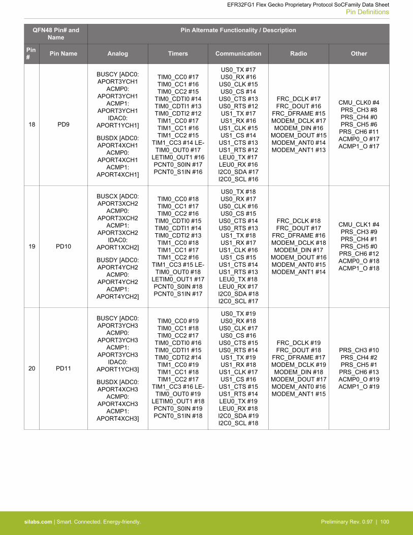
QFN48 Pin# andName
Pin Alternate Functionality / Description
Pin# Pin Name Analog Timers Communication Radio Other
18 PD9
BUSCY [ADC0:APORT3YCH1
ACMP0:APORT3YCH1
ACMP1:APORT3YCH1
IDAC0:APORT1YCH1]
BUSDX [ADC0:APORT4XCH1
ACMP0:APORT4XCH1
ACMP1:APORT4XCH1]
TIM0_CC0 #17TIM0_CC1 #16TIM0_CC2 #15
TIM0_CDTI0 #14TIM0_CDTI1 #13TIM0_CDTI2 #12TIM1_CC0 #17TIM1_CC1 #16TIM1_CC2 #15
TIM1_CC3 #14 LE-TIM0_OUT0 #17
LETIM0_OUT1 #16PCNT0_S0IN #17PCNT0_S1IN #16
US0_TX #17US0_RX #16
US0_CLK #15US0_CS #14
US0_CTS #13US0_RTS #12US1_TX #17US1_RX #16
US1_CLK #15US1_CS #14
US1_CTS #13US1_RTS #12LEU0_TX #17LEU0_RX #16I2C0_SDA #17I2C0_SCL #16
FRC_DCLK #17FRC_DOUT #16
FRC_DFRAME #15MODEM_DCLK #17MODEM_DIN #16
MODEM_DOUT #15MODEM_ANT0 #14MODEM_ANT1 #13
CMU_CLK0 #4PRS_CH3 #8PRS_CH4 #0PRS_CH5 #6
PRS_CH6 #11ACMP0_O #17ACMP1_O #17
19 PD10
BUSCX [ADC0:APORT3XCH2
ACMP0:APORT3XCH2
ACMP1:APORT3XCH2
IDAC0:APORT1XCH2]
BUSDY [ADC0:APORT4YCH2
ACMP0:APORT4YCH2
ACMP1:APORT4YCH2]
TIM0_CC0 #18TIM0_CC1 #17TIM0_CC2 #16
TIM0_CDTI0 #15TIM0_CDTI1 #14TIM0_CDTI2 #13TIM1_CC0 #18TIM1_CC1 #17TIM1_CC2 #16
TIM1_CC3 #15 LE-TIM0_OUT0 #18
LETIM0_OUT1 #17PCNT0_S0IN #18PCNT0_S1IN #17
US0_TX #18US0_RX #17
US0_CLK #16US0_CS #15
US0_CTS #14US0_RTS #13US1_TX #18US1_RX #17
US1_CLK #16US1_CS #15
US1_CTS #14US1_RTS #13LEU0_TX #18LEU0_RX #17I2C0_SDA #18I2C0_SCL #17
FRC_DCLK #18FRC_DOUT #17
FRC_DFRAME #16MODEM_DCLK #18MODEM_DIN #17
MODEM_DOUT #16MODEM_ANT0 #15MODEM_ANT1 #14
CMU_CLK1 #4PRS_CH3 #9PRS_CH4 #1PRS_CH5 #0
PRS_CH6 #12ACMP0_O #18ACMP1_O #18
20 PD11
BUSCY [ADC0:APORT3YCH3
ACMP0:APORT3YCH3
ACMP1:APORT3YCH3
IDAC0:APORT1YCH3]
BUSDX [ADC0:APORT4XCH3
ACMP0:APORT4XCH3
ACMP1:APORT4XCH3]
TIM0_CC0 #19TIM0_CC1 #18TIM0_CC2 #17
TIM0_CDTI0 #16TIM0_CDTI1 #15TIM0_CDTI2 #14TIM1_CC0 #19TIM1_CC1 #18TIM1_CC2 #17
TIM1_CC3 #16 LE-TIM0_OUT0 #19
LETIM0_OUT1 #18PCNT0_S0IN #19PCNT0_S1IN #18
US0_TX #19US0_RX #18
US0_CLK #17US0_CS #16
US0_CTS #15US0_RTS #14US1_TX #19US1_RX #18
US1_CLK #17US1_CS #16
US1_CTS #15US1_RTS #14LEU0_TX #19LEU0_RX #18I2C0_SDA #19I2C0_SCL #18
FRC_DCLK #19FRC_DOUT #18
FRC_DFRAME #17MODEM_DCLK #19MODEM_DIN #18
MODEM_DOUT #17MODEM_ANT0 #16MODEM_ANT1 #15
PRS_CH3 #10PRS_CH4 #2PRS_CH5 #1
PRS_CH6 #13ACMP0_O #19ACMP1_O #19
EFR32FG1 Flex Gecko Proprietary Protocol SoCFamily Data SheetPin Definitions
silabs.com | Smart. Connected. Energy-friendly. Preliminary Rev. 0.97 | 100
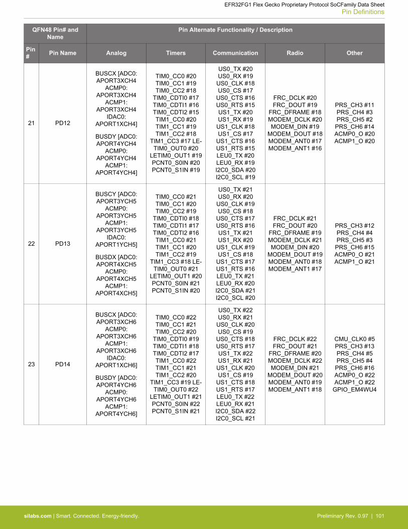
QFN48 Pin# andName
Pin Alternate Functionality / Description
Pin# Pin Name Analog Timers Communication Radio Other
21 PD12
BUSCX [ADC0:APORT3XCH4
ACMP0:APORT3XCH4
ACMP1:APORT3XCH4
IDAC0:APORT1XCH4]
BUSDY [ADC0:APORT4YCH4
ACMP0:APORT4YCH4
ACMP1:APORT4YCH4]
TIM0_CC0 #20TIM0_CC1 #19TIM0_CC2 #18
TIM0_CDTI0 #17TIM0_CDTI1 #16TIM0_CDTI2 #15TIM1_CC0 #20TIM1_CC1 #19TIM1_CC2 #18
TIM1_CC3 #17 LE-TIM0_OUT0 #20
LETIM0_OUT1 #19PCNT0_S0IN #20PCNT0_S1IN #19
US0_TX #20US0_RX #19
US0_CLK #18US0_CS #17
US0_CTS #16US0_RTS #15US1_TX #20US1_RX #19
US1_CLK #18US1_CS #17
US1_CTS #16US1_RTS #15LEU0_TX #20LEU0_RX #19I2C0_SDA #20I2C0_SCL #19
FRC_DCLK #20FRC_DOUT #19
FRC_DFRAME #18MODEM_DCLK #20MODEM_DIN #19
MODEM_DOUT #18MODEM_ANT0 #17MODEM_ANT1 #16
PRS_CH3 #11PRS_CH4 #3PRS_CH5 #2
PRS_CH6 #14ACMP0_O #20ACMP1_O #20
22 PD13
BUSCY [ADC0:APORT3YCH5
ACMP0:APORT3YCH5
ACMP1:APORT3YCH5
IDAC0:APORT1YCH5]
BUSDX [ADC0:APORT4XCH5
ACMP0:APORT4XCH5
ACMP1:APORT4XCH5]
TIM0_CC0 #21TIM0_CC1 #20TIM0_CC2 #19
TIM0_CDTI0 #18TIM0_CDTI1 #17TIM0_CDTI2 #16TIM1_CC0 #21TIM1_CC1 #20TIM1_CC2 #19
TIM1_CC3 #18 LE-TIM0_OUT0 #21
LETIM0_OUT1 #20PCNT0_S0IN #21PCNT0_S1IN #20
US0_TX #21US0_RX #20
US0_CLK #19US0_CS #18
US0_CTS #17US0_RTS #16US1_TX #21US1_RX #20
US1_CLK #19US1_CS #18
US1_CTS #17US1_RTS #16LEU0_TX #21LEU0_RX #20I2C0_SDA #21I2C0_SCL #20
FRC_DCLK #21FRC_DOUT #20
FRC_DFRAME #19MODEM_DCLK #21MODEM_DIN #20
MODEM_DOUT #19MODEM_ANT0 #18MODEM_ANT1 #17
PRS_CH3 #12PRS_CH4 #4PRS_CH5 #3
PRS_CH6 #15ACMP0_O #21ACMP1_O #21
23 PD14
BUSCX [ADC0:APORT3XCH6
ACMP0:APORT3XCH6
ACMP1:APORT3XCH6
IDAC0:APORT1XCH6]
BUSDY [ADC0:APORT4YCH6
ACMP0:APORT4YCH6
ACMP1:APORT4YCH6]
TIM0_CC0 #22TIM0_CC1 #21TIM0_CC2 #20
TIM0_CDTI0 #19TIM0_CDTI1 #18TIM0_CDTI2 #17TIM1_CC0 #22TIM1_CC1 #21TIM1_CC2 #20
TIM1_CC3 #19 LE-TIM0_OUT0 #22
LETIM0_OUT1 #21PCNT0_S0IN #22PCNT0_S1IN #21
US0_TX #22US0_RX #21
US0_CLK #20US0_CS #19
US0_CTS #18US0_RTS #17US1_TX #22US1_RX #21
US1_CLK #20US1_CS #19
US1_CTS #18US1_RTS #17LEU0_TX #22LEU0_RX #21I2C0_SDA #22I2C0_SCL #21
FRC_DCLK #22FRC_DOUT #21
FRC_DFRAME #20MODEM_DCLK #22MODEM_DIN #21
MODEM_DOUT #20MODEM_ANT0 #19MODEM_ANT1 #18
CMU_CLK0 #5PRS_CH3 #13PRS_CH4 #5PRS_CH5 #4
PRS_CH6 #16ACMP0_O #22ACMP1_O #22
GPIO_EM4WU4
EFR32FG1 Flex Gecko Proprietary Protocol SoCFamily Data SheetPin Definitions
silabs.com | Smart. Connected. Energy-friendly. Preliminary Rev. 0.97 | 101

QFN48 Pin# andName
Pin Alternate Functionality / Description
Pin# Pin Name Analog Timers Communication Radio Other
24 PD15
BUSCY [ADC0:APORT3YCH7
ACMP0:APORT3YCH7
ACMP1:APORT3YCH7
IDAC0:APORT1YCH7]
BUSDX [ADC0:APORT4XCH7
ACMP0:APORT4XCH7
ACMP1:APORT4XCH7]
TIM0_CC0 #23TIM0_CC1 #22TIM0_CC2 #21
TIM0_CDTI0 #20TIM0_CDTI1 #19TIM0_CDTI2 #18TIM1_CC0 #23TIM1_CC1 #22TIM1_CC2 #21
TIM1_CC3 #20 LE-TIM0_OUT0 #23
LETIM0_OUT1 #22PCNT0_S0IN #23PCNT0_S1IN #22
US0_TX #23US0_RX #22
US0_CLK #21US0_CS #20
US0_CTS #19US0_RTS #18US1_TX #23US1_RX #22
US1_CLK #21US1_CS #20
US1_CTS #19US1_RTS #18LEU0_TX #23LEU0_RX #22I2C0_SDA #23I2C0_SCL #22
FRC_DCLK #23FRC_DOUT #22
FRC_DFRAME #21MODEM_DCLK #23MODEM_DIN #22
MODEM_DOUT #21MODEM_ANT0 #20MODEM_ANT1 #19
CMU_CLK1 #5PRS_CH3 #14PRS_CH4 #6PRS_CH5 #5
PRS_CH6 #17ACMP0_O #23ACMP1_O #23DBG_SWO #2
25 PA0
ADC0_EXTN
BUSCX [ADC0:APORT3XCH8
ACMP0:APORT3XCH8
ACMP1:APORT3XCH8
IDAC0:APORT1XCH8]
BUSDY [ADC0:APORT4YCH8
ACMP0:APORT4YCH8
ACMP1:APORT4YCH8]
TIM0_CC0 #0TIM0_CC1 #31TIM0_CC2 #30
TIM0_CDTI0 #29TIM0_CDTI1 #28TIM0_CDTI2 #27
TIM1_CC0 #0TIM1_CC1 #31TIM1_CC2 #30
TIM1_CC3 #29 LE-TIM0_OUT0 #0 LE-
TIM0_OUT1 #31PCNT0_S0IN #0PCNT0_S1IN #31
US0_TX #0US0_RX #31
US0_CLK #30US0_CS #29
US0_CTS #28US0_RTS #27
US1_TX #0US1_RX #31
US1_CLK #30US1_CS #29
US1_CTS #28US1_RTS #27LEU0_TX #0
LEU0_RX #31I2C0_SDA #0I2C0_SCL #31
FRC_DCLK #0FRC_DOUT #31
FRC_DFRAME #30MODEM_DCLK #0MODEM_DIN #31
MODEM_DOUT #30MODEM_ANT0 #29MODEM_ANT1 #28
CMU_CLK1 #0PRS_CH6 #0
PRS_CH7 #10PRS_CH8 #9PRS_CH9 #8ACMP0_O #0ACMP1_O #0
26 PA1
ADC0_EXTP
BUSCY [ADC0:APORT3YCH9
ACMP0:APORT3YCH9
ACMP1:APORT3YCH9
IDAC0:APORT1YCH9]
BUSDX [ADC0:APORT4XCH9
ACMP0:APORT4XCH9
ACMP1:APORT4XCH9]
TIM0_CC0 #1TIM0_CC1 #0TIM0_CC2 #31
TIM0_CDTI0 #30TIM0_CDTI1 #29TIM0_CDTI2 #28
TIM1_CC0 #1TIM1_CC1 #0TIM1_CC2 #31
TIM1_CC3 #30 LE-TIM0_OUT0 #1 LE-
TIM0_OUT1 #0PCNT0_S0IN #1PCNT0_S1IN #0
US0_TX #1US0_RX #0
US0_CLK #31US0_CS #30
US0_CTS #29US0_RTS #28
US1_TX #1US1_RX #0
US1_CLK #31US1_CS #30
US1_CTS #29US1_RTS #28LEU0_TX #1LEU0_RX #0I2C0_SDA #1I2C0_SCL #0
FRC_DCLK #1FRC_DOUT #0
FRC_DFRAME #31MODEM_DCLK #1MODEM_DIN #0
MODEM_DOUT #31MODEM_ANT0 #30MODEM_ANT1 #29
CMU_CLK0 #0PRS_CH6 #1PRS_CH7 #0
PRS_CH8 #10PRS_CH9 #9ACMP0_O #1ACMP1_O #1
EFR32FG1 Flex Gecko Proprietary Protocol SoCFamily Data SheetPin Definitions
silabs.com | Smart. Connected. Energy-friendly. Preliminary Rev. 0.97 | 102
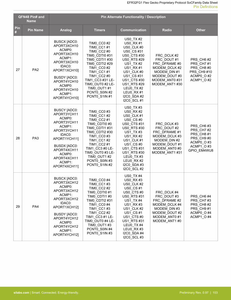
QFN48 Pin# andName
Pin Alternate Functionality / Description
Pin# Pin Name Analog Timers Communication Radio Other
27 PA2
BUSCX [ADC0:APORT3XCH10
ACMP0:APORT3XCH10
ACMP1:APORT3XCH10
IDAC0:APORT1XCH10]
BUSDY [ADC0:APORT4YCH10
ACMP0:APORT4YCH10
ACMP1:APORT4YCH10]
TIM0_CC0 #2TIM0_CC1 #1TIM0_CC2 #0
TIM0_CDTI0 #31TIM0_CDTI1 #30TIM0_CDTI2 #29
TIM1_CC0 #2TIM1_CC1 #1TIM1_CC2 #0
TIM1_CC3 #31 LE-TIM0_OUT0 #2 LE-
TIM0_OUT1 #1PCNT0_S0IN #2PCNT0_S1IN #1
US0_TX #2US0_RX #1
US0_CLK #0US0_CS #31
US0_CTS #30US0_RTS #29
US1_TX #2US1_RX #1
US1_CLK #0US1_CS #31
US1_CTS #30US1_RTS #29LEU0_TX #2LEU0_RX #1I2C0_SDA #2I2C0_SCL #1
FRC_DCLK #2FRC_DOUT #1
FRC_DFRAME #0MODEM_DCLK #2MODEM_DIN #1
MODEM_DOUT #0MODEM_ANT0 #31MODEM_ANT1 #30
PRS_CH6 #2PRS_CH7 #1PRS_CH8 #0
PRS_CH9 #10ACMP0_O #2ACMP1_O #2
28 PA3
BUSCY [ADC0:APORT3YCH11
ACMP0:APORT3YCH11
ACMP1:APORT3YCH11
IDAC0:APORT1YCH11]
BUSDX [ADC0:APORT4XCH11
ACMP0:APORT4XCH11
ACMP1:APORT4XCH11]
TIM0_CC0 #3TIM0_CC1 #2TIM0_CC2 #1
TIM0_CDTI0 #0TIM0_CDTI1 #31TIM0_CDTI2 #30
TIM1_CC0 #3TIM1_CC1 #2TIM1_CC2 #1
TIM1_CC3 #0 LE-TIM0_OUT0 #3 LE-
TIM0_OUT1 #2PCNT0_S0IN #3PCNT0_S1IN #2
US0_TX #3US0_RX #2
US0_CLK #1US0_CS #0
US0_CTS #31US0_RTS #30
US1_TX #3US1_RX #2
US1_CLK #1US1_CS #0
US1_CTS #31US1_RTS #30LEU0_TX #3LEU0_RX #2I2C0_SDA #3I2C0_SCL #2
FRC_DCLK #3FRC_DOUT #2
FRC_DFRAME #1MODEM_DCLK #3MODEM_DIN #2
MODEM_DOUT #1MODEM_ANT0 #0
MODEM_ANT1 #31
PRS_CH6 #3PRS_CH7 #2PRS_CH8 #1PRS_CH9 #0ACMP0_O #3ACMP1_O #3
GPIO_EM4WU8
29 PA4
BUSCX [ADC0:APORT3XCH12
ACMP0:APORT3XCH12
ACMP1:APORT3XCH12
IDAC0:APORT1XCH12]
BUSDY [ADC0:APORT4YCH12
ACMP0:APORT4YCH12
ACMP1:APORT4YCH12]
TIM0_CC0 #4TIM0_CC1 #3TIM0_CC2 #2
TIM0_CDTI0 #1TIM0_CDTI1 #0TIM0_CDTI2 #31
TIM1_CC0 #4TIM1_CC1 #3TIM1_CC2 #2
TIM1_CC3 #1 LE-TIM0_OUT0 #4 LE-
TIM0_OUT1 #3PCNT0_S0IN #4PCNT0_S1IN #3
US0_TX #4US0_RX #3
US0_CLK #2US0_CS #1
US0_CTS #0US0_RTS #31
US1_TX #4US1_RX #3
US1_CLK #2US1_CS #1
US1_CTS #0US1_RTS #31LEU0_TX #4LEU0_RX #3I2C0_SDA #4I2C0_SCL #3
FRC_DCLK #4FRC_DOUT #3
FRC_DFRAME #2MODEM_DCLK #4MODEM_DIN #3
MODEM_DOUT #2MODEM_ANT0 #1MODEM_ANT1 #0
PRS_CH6 #4PRS_CH7 #3PRS_CH8 #2PRS_CH9 #1ACMP0_O #4ACMP1_O #4
EFR32FG1 Flex Gecko Proprietary Protocol SoCFamily Data SheetPin Definitions
silabs.com | Smart. Connected. Energy-friendly. Preliminary Rev. 0.97 | 103

QFN48 Pin# andName
Pin Alternate Functionality / Description
Pin# Pin Name Analog Timers Communication Radio Other
30 PA5
BUSCY [ADC0:APORT3YCH13
ACMP0:APORT3YCH13
ACMP1:APORT3YCH13
IDAC0:APORT1YCH13]
BUSDX [ADC0:APORT4XCH13
ACMP0:APORT4XCH13
ACMP1:APORT4XCH13]
TIM0_CC0 #5TIM0_CC1 #4TIM0_CC2 #3
TIM0_CDTI0 #2TIM0_CDTI1 #1TIM0_CDTI2 #0TIM1_CC0 #5TIM1_CC1 #4TIM1_CC2 #3
TIM1_CC3 #2 LE-TIM0_OUT0 #5 LE-
TIM0_OUT1 #4PCNT0_S0IN #5PCNT0_S1IN #4
US0_TX #5US0_RX #4
US0_CLK #3US0_CS #2
US0_CTS #1US0_RTS #0US1_TX #5US1_RX #4
US1_CLK #3US1_CS #2
US1_CTS #1US1_RTS #0LEU0_TX #5LEU0_RX #4I2C0_SDA #5I2C0_SCL #4
FRC_DCLK #5FRC_DOUT #4
FRC_DFRAME #3MODEM_DCLK #5MODEM_DIN #4
MODEM_DOUT #3MODEM_ANT0 #2MODEM_ANT1 #1
PRS_CH6 #5PRS_CH7 #4PRS_CH8 #3PRS_CH9 #2ACMP0_O #5ACMP1_O #5
31 PB11
BUSCY [ADC0:APORT3YCH27
ACMP0:APORT3YCH27
ACMP1:APORT3YCH27
IDAC0:APORT1YCH27]
BUSDX [ADC0:APORT4XCH27
ACMP0:APORT4XCH27
ACMP1:APORT4XCH27]
TIM0_CC0 #6TIM0_CC1 #5TIM0_CC2 #4
TIM0_CDTI0 #3TIM0_CDTI1 #2TIM0_CDTI2 #1TIM1_CC0 #6TIM1_CC1 #5TIM1_CC2 #4
TIM1_CC3 #3 LE-TIM0_OUT0 #6 LE-
TIM0_OUT1 #5PCNT0_S0IN #6PCNT0_S1IN #5
US0_TX #6US0_RX #5
US0_CLK #4US0_CS #3
US0_CTS #2US0_RTS #1US1_TX #6US1_RX #5
US1_CLK #4US1_CS #3
US1_CTS #2US1_RTS #1LEU0_TX #6LEU0_RX #5I2C0_SDA #6I2C0_SCL #5
FRC_DCLK #6FRC_DOUT #5
FRC_DFRAME #4MODEM_DCLK #6MODEM_DIN #5
MODEM_DOUT #4MODEM_ANT0 #3MODEM_ANT1 #2
PRS_CH6 #6PRS_CH7 #5PRS_CH8 #4PRS_CH9 #3ACMP0_O #6ACMP1_O #6
32 PB12
BUSCX [ADC0:APORT3XCH28
ACMP0:APORT3XCH28
ACMP1:APORT3XCH28
IDAC0:APORT1XCH28]
BUSDY [ADC0:APORT4YCH28
ACMP0:APORT4YCH28
ACMP1:APORT4YCH28]
TIM0_CC0 #7TIM0_CC1 #6TIM0_CC2 #5
TIM0_CDTI0 #4TIM0_CDTI1 #3TIM0_CDTI2 #2TIM1_CC0 #7TIM1_CC1 #6TIM1_CC2 #5
TIM1_CC3 #4 LE-TIM0_OUT0 #7 LE-
TIM0_OUT1 #6PCNT0_S0IN #7PCNT0_S1IN #6
US0_TX #7US0_RX #6
US0_CLK #5US0_CS #4
US0_CTS #3US0_RTS #2US1_TX #7US1_RX #6
US1_CLK #5US1_CS #4
US1_CTS #3US1_RTS #2LEU0_TX #7LEU0_RX #6I2C0_SDA #7I2C0_SCL #6
FRC_DCLK #7FRC_DOUT #6
FRC_DFRAME #5MODEM_DCLK #7MODEM_DIN #6
MODEM_DOUT #5MODEM_ANT0 #4MODEM_ANT1 #3
PRS_CH6 #7PRS_CH7 #6PRS_CH8 #5PRS_CH9 #4ACMP0_O #7ACMP1_O #7
EFR32FG1 Flex Gecko Proprietary Protocol SoCFamily Data SheetPin Definitions
silabs.com | Smart. Connected. Energy-friendly. Preliminary Rev. 0.97 | 104
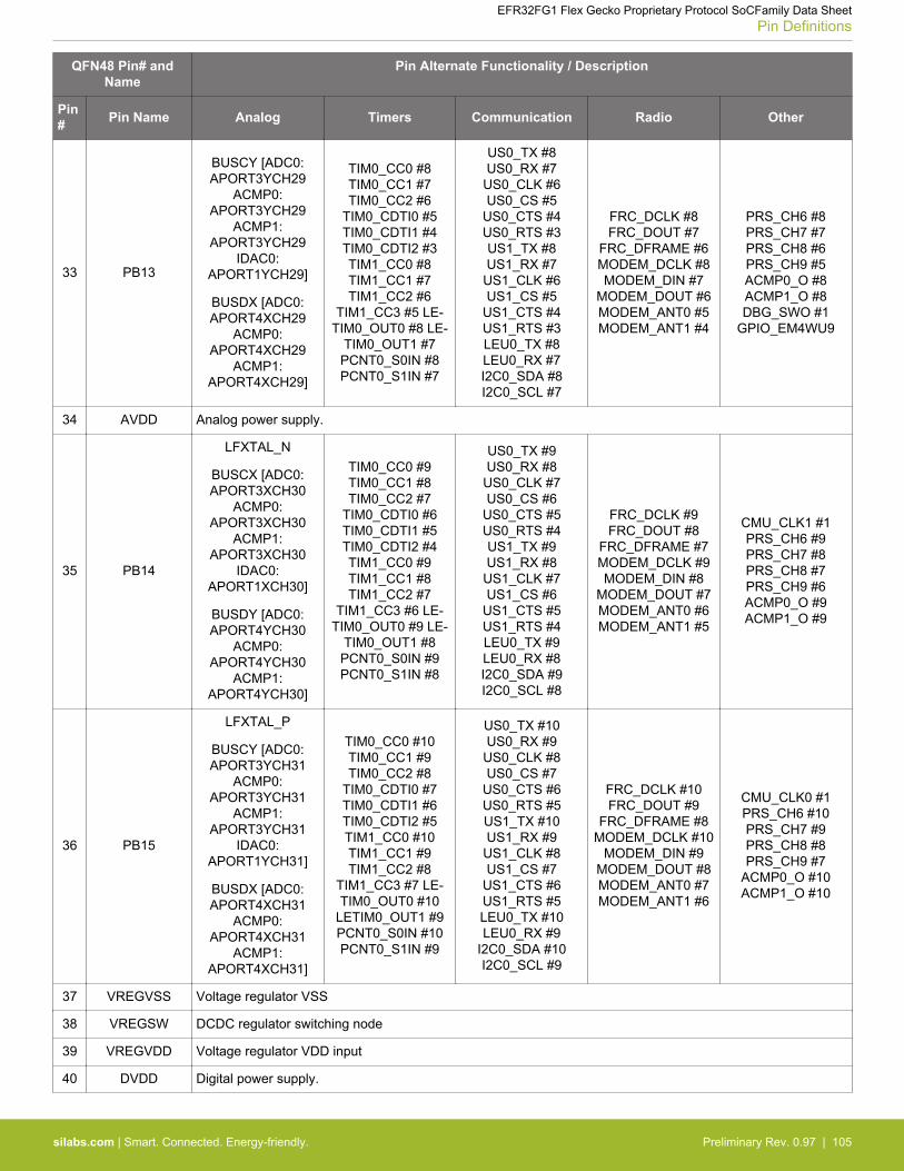
QFN48 Pin# andName
Pin Alternate Functionality / Description
Pin# Pin Name Analog Timers Communication Radio Other
33 PB13
BUSCY [ADC0:APORT3YCH29
ACMP0:APORT3YCH29
ACMP1:APORT3YCH29
IDAC0:APORT1YCH29]
BUSDX [ADC0:APORT4XCH29
ACMP0:APORT4XCH29
ACMP1:APORT4XCH29]
TIM0_CC0 #8TIM0_CC1 #7TIM0_CC2 #6
TIM0_CDTI0 #5TIM0_CDTI1 #4TIM0_CDTI2 #3TIM1_CC0 #8TIM1_CC1 #7TIM1_CC2 #6
TIM1_CC3 #5 LE-TIM0_OUT0 #8 LE-
TIM0_OUT1 #7PCNT0_S0IN #8PCNT0_S1IN #7
US0_TX #8US0_RX #7
US0_CLK #6US0_CS #5
US0_CTS #4US0_RTS #3US1_TX #8US1_RX #7
US1_CLK #6US1_CS #5
US1_CTS #4US1_RTS #3LEU0_TX #8LEU0_RX #7I2C0_SDA #8I2C0_SCL #7
FRC_DCLK #8FRC_DOUT #7
FRC_DFRAME #6MODEM_DCLK #8MODEM_DIN #7
MODEM_DOUT #6MODEM_ANT0 #5MODEM_ANT1 #4
PRS_CH6 #8PRS_CH7 #7PRS_CH8 #6PRS_CH9 #5ACMP0_O #8ACMP1_O #8DBG_SWO #1
GPIO_EM4WU9
34 AVDD Analog power supply.
35 PB14
LFXTAL_N
BUSCX [ADC0:APORT3XCH30
ACMP0:APORT3XCH30
ACMP1:APORT3XCH30
IDAC0:APORT1XCH30]
BUSDY [ADC0:APORT4YCH30
ACMP0:APORT4YCH30
ACMP1:APORT4YCH30]
TIM0_CC0 #9TIM0_CC1 #8TIM0_CC2 #7
TIM0_CDTI0 #6TIM0_CDTI1 #5TIM0_CDTI2 #4TIM1_CC0 #9TIM1_CC1 #8TIM1_CC2 #7
TIM1_CC3 #6 LE-TIM0_OUT0 #9 LE-
TIM0_OUT1 #8PCNT0_S0IN #9PCNT0_S1IN #8
US0_TX #9US0_RX #8
US0_CLK #7US0_CS #6
US0_CTS #5US0_RTS #4US1_TX #9US1_RX #8
US1_CLK #7US1_CS #6
US1_CTS #5US1_RTS #4LEU0_TX #9LEU0_RX #8I2C0_SDA #9I2C0_SCL #8
FRC_DCLK #9FRC_DOUT #8
FRC_DFRAME #7MODEM_DCLK #9MODEM_DIN #8
MODEM_DOUT #7MODEM_ANT0 #6MODEM_ANT1 #5
CMU_CLK1 #1PRS_CH6 #9PRS_CH7 #8PRS_CH8 #7PRS_CH9 #6ACMP0_O #9ACMP1_O #9
36 PB15
LFXTAL_P
BUSCY [ADC0:APORT3YCH31
ACMP0:APORT3YCH31
ACMP1:APORT3YCH31
IDAC0:APORT1YCH31]
BUSDX [ADC0:APORT4XCH31
ACMP0:APORT4XCH31
ACMP1:APORT4XCH31]
TIM0_CC0 #10TIM0_CC1 #9TIM0_CC2 #8
TIM0_CDTI0 #7TIM0_CDTI1 #6TIM0_CDTI2 #5TIM1_CC0 #10TIM1_CC1 #9TIM1_CC2 #8
TIM1_CC3 #7 LE-TIM0_OUT0 #10
LETIM0_OUT1 #9PCNT0_S0IN #10PCNT0_S1IN #9
US0_TX #10US0_RX #9
US0_CLK #8US0_CS #7
US0_CTS #6US0_RTS #5US1_TX #10US1_RX #9
US1_CLK #8US1_CS #7
US1_CTS #6US1_RTS #5LEU0_TX #10LEU0_RX #9
I2C0_SDA #10I2C0_SCL #9
FRC_DCLK #10FRC_DOUT #9
FRC_DFRAME #8MODEM_DCLK #10
MODEM_DIN #9MODEM_DOUT #8MODEM_ANT0 #7MODEM_ANT1 #6
CMU_CLK0 #1PRS_CH6 #10PRS_CH7 #9PRS_CH8 #8PRS_CH9 #7
ACMP0_O #10ACMP1_O #10
37 VREGVSS Voltage regulator VSS
38 VREGSW DCDC regulator switching node
39 VREGVDD Voltage regulator VDD input
40 DVDD Digital power supply.
EFR32FG1 Flex Gecko Proprietary Protocol SoCFamily Data SheetPin Definitions
silabs.com | Smart. Connected. Energy-friendly. Preliminary Rev. 0.97 | 105
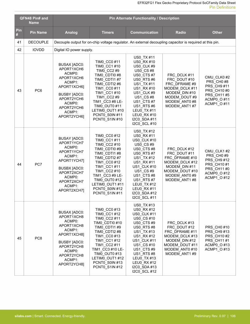
QFN48 Pin# andName
Pin Alternate Functionality / Description
Pin# Pin Name Analog Timers Communication Radio Other
41 DECOUPLE Decouple output for on-chip voltage regulator. An external decoupling capacitor is required at this pin.
42 IOVDD Digital IO power supply.
43 PC6
BUSAX [ADC0:APORT1XCH6
ACMP0:APORT1XCH6
ACMP1:APORT1XCH6]
BUSBY [ADC0:APORT2YCH6
ACMP0:APORT2YCH6
ACMP1:APORT2YCH6]
TIM0_CC0 #11TIM0_CC1 #10TIM0_CC2 #9
TIM0_CDTI0 #8TIM0_CDTI1 #7TIM0_CDTI2 #6TIM1_CC0 #11TIM1_CC1 #10TIM1_CC2 #9
TIM1_CC3 #8 LE-TIM0_OUT0 #11
LETIM0_OUT1 #10PCNT0_S0IN #11PCNT0_S1IN #10
US0_TX #11US0_RX #10US0_CLK #9US0_CS #8
US0_CTS #7US0_RTS #6US1_TX #11US1_RX #10US1_CLK #9US1_CS #8
US1_CTS #7US1_RTS #6LEU0_TX #11LEU0_RX #10I2C0_SDA #11I2C0_SCL #10
FRC_DCLK #11FRC_DOUT #10
FRC_DFRAME #9MODEM_DCLK #11MODEM_DIN #10
MODEM_DOUT #9MODEM_ANT0 #8MODEM_ANT1 #7
CMU_CLK0 #2PRS_CH0 #8
PRS_CH9 #11PRS_CH10 #0PRS_CH11 #5ACMP0_O #11ACMP1_O #11
44 PC7
BUSAY [ADC0:APORT1YCH7
ACMP0:APORT1YCH7
ACMP1:APORT1YCH7]
BUSBX [ADC0:APORT2XCH7
ACMP0:APORT2XCH7
ACMP1:APORT2XCH7]
TIM0_CC0 #12TIM0_CC1 #11TIM0_CC2 #10TIM0_CDTI0 #9TIM0_CDTI1 #8TIM0_CDTI2 #7TIM1_CC0 #12TIM1_CC1 #11TIM1_CC2 #10
TIM1_CC3 #9 LE-TIM0_OUT0 #12
LETIM0_OUT1 #11PCNT0_S0IN #12PCNT0_S1IN #11
US0_TX #12US0_RX #11
US0_CLK #10US0_CS #9
US0_CTS #8US0_RTS #7US1_TX #12US1_RX #11
US1_CLK #10US1_CS #9
US1_CTS #8US1_RTS #7LEU0_TX #12LEU0_RX #11I2C0_SDA #12I2C0_SCL #11
FRC_DCLK #12FRC_DOUT #11
FRC_DFRAME #10MODEM_DCLK #12MODEM_DIN #11
MODEM_DOUT #10MODEM_ANT0 #9MODEM_ANT1 #8
CMU_CLK1 #2PRS_CH0 #9
PRS_CH9 #12PRS_CH10 #1PRS_CH11 #0ACMP0_O #12ACMP1_O #12
45 PC8
BUSAX [ADC0:APORT1XCH8
ACMP0:APORT1XCH8
ACMP1:APORT1XCH8]
BUSBY [ADC0:APORT2YCH8
ACMP0:APORT2YCH8
ACMP1:APORT2YCH8]
TIM0_CC0 #13TIM0_CC1 #12TIM0_CC2 #11
TIM0_CDTI0 #10TIM0_CDTI1 #9TIM0_CDTI2 #8TIM1_CC0 #13TIM1_CC1 #12TIM1_CC2 #11
TIM1_CC3 #10 LE-TIM0_OUT0 #13
LETIM0_OUT1 #12PCNT0_S0IN #13PCNT0_S1IN #12
US0_TX #13US0_RX #12
US0_CLK #11US0_CS #10US0_CTS #9US0_RTS #8US1_TX #13US1_RX #12
US1_CLK #11US1_CS #10US1_CTS #9US1_RTS #8LEU0_TX #13LEU0_RX #12I2C0_SDA #13I2C0_SCL #12
FRC_DCLK #13FRC_DOUT #12
FRC_DFRAME #11MODEM_DCLK #13MODEM_DIN #12
MODEM_DOUT #11MODEM_ANT0 #10MODEM_ANT1 #9
PRS_CH0 #10PRS_CH9 #13PRS_CH10 #2PRS_CH11 #1ACMP0_O #13ACMP1_O #13
EFR32FG1 Flex Gecko Proprietary Protocol SoCFamily Data SheetPin Definitions
silabs.com | Smart. Connected. Energy-friendly. Preliminary Rev. 0.97 | 106

QFN48 Pin# andName
Pin Alternate Functionality / Description
Pin# Pin Name Analog Timers Communication Radio Other
46 PC9
BUSAY [ADC0:APORT1YCH9
ACMP0:APORT1YCH9
ACMP1:APORT1YCH9]
BUSBX [ADC0:APORT2XCH9
ACMP0:APORT2XCH9
ACMP1:APORT2XCH9]
TIM0_CC0 #14TIM0_CC1 #13TIM0_CC2 #12
TIM0_CDTI0 #11TIM0_CDTI1 #10TIM0_CDTI2 #9TIM1_CC0 #14TIM1_CC1 #13TIM1_CC2 #12
TIM1_CC3 #11 LE-TIM0_OUT0 #14
LETIM0_OUT1 #13PCNT0_S0IN #14PCNT0_S1IN #13
US0_TX #14US0_RX #13
US0_CLK #12US0_CS #11
US0_CTS #10US0_RTS #9US1_TX #14US1_RX #13
US1_CLK #12US1_CS #11
US1_CTS #10US1_RTS #9LEU0_TX #14LEU0_RX #13I2C0_SDA #14I2C0_SCL #13
FRC_DCLK #14FRC_DOUT #13
FRC_DFRAME #12MODEM_DCLK #14MODEM_DIN #13
MODEM_DOUT #12MODEM_ANT0 #11MODEM_ANT1 #10
PRS_CH0 #11PRS_CH9 #14PRS_CH10 #3PRS_CH11 #2ACMP0_O #14ACMP1_O #14
47 PC10
BUSAX [ADC0:APORT1XCH10
ACMP0:APORT1XCH10
ACMP1:APORT1XCH10]
BUSBY [ADC0:APORT2YCH10
ACMP0:APORT2YCH10
ACMP1:APORT2YCH10]
TIM0_CC0 #15TIM0_CC1 #14TIM0_CC2 #13
TIM0_CDTI0 #12TIM0_CDTI1 #11TIM0_CDTI2 #10TIM1_CC0 #15TIM1_CC1 #14TIM1_CC2 #13
TIM1_CC3 #12 LE-TIM0_OUT0 #15
LETIM0_OUT1 #14PCNT0_S0IN #15PCNT0_S1IN #14
US0_TX #15US0_RX #14
US0_CLK #13US0_CS #12
US0_CTS #11US0_RTS #10US1_TX #15US1_RX #14
US1_CLK #13US1_CS #12
US1_CTS #11US1_RTS #10LEU0_TX #15LEU0_RX #14I2C0_SDA #15I2C0_SCL #14
FRC_DCLK #15FRC_DOUT #14
FRC_DFRAME #13MODEM_DCLK #15MODEM_DIN #14
MODEM_DOUT #13MODEM_ANT0 #12MODEM_ANT1 #11
CMU_CLK1 #3PRS_CH0 #12PRS_CH9 #15PRS_CH10 #4PRS_CH11 #3ACMP0_O #15ACMP1_O #15
GPIO_EM4WU12
48 PC11
BUSAY [ADC0:APORT1YCH11
ACMP0:APORT1YCH11
ACMP1:APORT1YCH11]
BUSBX [ADC0:APORT2XCH11
ACMP0:APORT2XCH11
ACMP1:APORT2XCH11]
TIM0_CC0 #16TIM0_CC1 #15TIM0_CC2 #14
TIM0_CDTI0 #13TIM0_CDTI1 #12TIM0_CDTI2 #11TIM1_CC0 #16TIM1_CC1 #15TIM1_CC2 #14
TIM1_CC3 #13 LE-TIM0_OUT0 #16
LETIM0_OUT1 #15PCNT0_S0IN #16PCNT0_S1IN #15
US0_TX #16US0_RX #15
US0_CLK #14US0_CS #13
US0_CTS #12US0_RTS #11US1_TX #16US1_RX #15
US1_CLK #14US1_CS #13
US1_CTS #12US1_RTS #11LEU0_TX #16LEU0_RX #15I2C0_SDA #16I2C0_SCL #15
FRC_DCLK #16FRC_DOUT #15
FRC_DFRAME #14MODEM_DCLK #16MODEM_DIN #15
MODEM_DOUT #14MODEM_ANT0 #13MODEM_ANT1 #12
CMU_CLK0 #3PRS_CH0 #13PRS_CH9 #16PRS_CH10 #5PRS_CH11 #4ACMP0_O #16ACMP1_O #16DBG_SWO #3
EFR32FG1 Flex Gecko Proprietary Protocol SoCFamily Data SheetPin Definitions
silabs.com | Smart. Connected. Energy-friendly. Preliminary Rev. 0.97 | 107
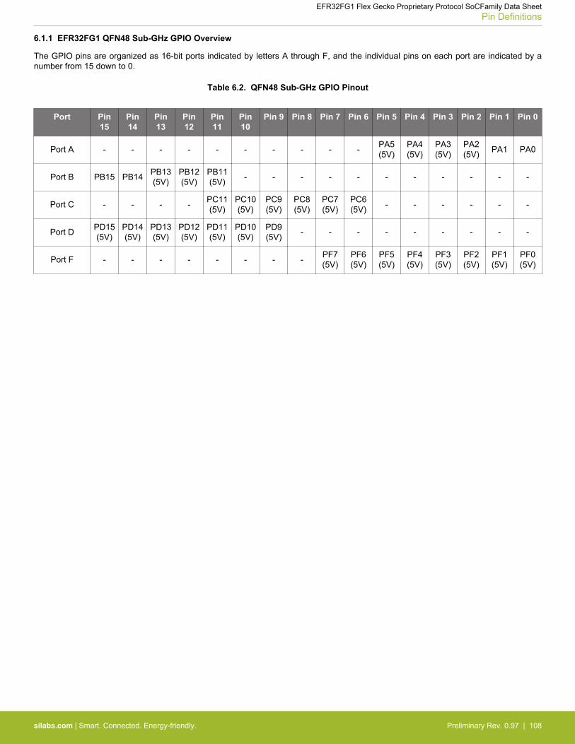
6.1.1 EFR32FG1 QFN48 Sub-GHz GPIO Overview
The GPIO pins are organized as 16-bit ports indicated by letters A through F, and the individual pins on each port are indicated by anumber from 15 down to 0.
Table 6.2. QFN48 Sub-GHz GPIO Pinout
Port Pin15
Pin14
Pin13
Pin12
Pin11
Pin10
Pin 9 Pin 8 Pin 7 Pin 6 Pin 5 Pin 4 Pin 3 Pin 2 Pin 1 Pin 0
Port A - - - - - - - - - - PA5(5V)
PA4(5V)
PA3(5V)
PA2(5V) PA1 PA0
Port B PB15 PB14 PB13(5V)
PB12(5V)
PB11(5V) - - - - - - - - - - -
Port C - - - - PC11(5V)
PC10(5V)
PC9(5V)
PC8(5V)
PC7(5V)
PC6(5V) - - - - - -
Port D PD15(5V)
PD14(5V)
PD13(5V)
PD12(5V)
PD11(5V)
PD10(5V)
PD9(5V) - - - - - - - - -
Port F - - - - - - - - PF7(5V)
PF6(5V)
PF5(5V)
PF4(5V)
PF3(5V)
PF2(5V)
PF1(5V)
PF0(5V)
EFR32FG1 Flex Gecko Proprietary Protocol SoCFamily Data SheetPin Definitions
silabs.com | Smart. Connected. Energy-friendly. Preliminary Rev. 0.97 | 108
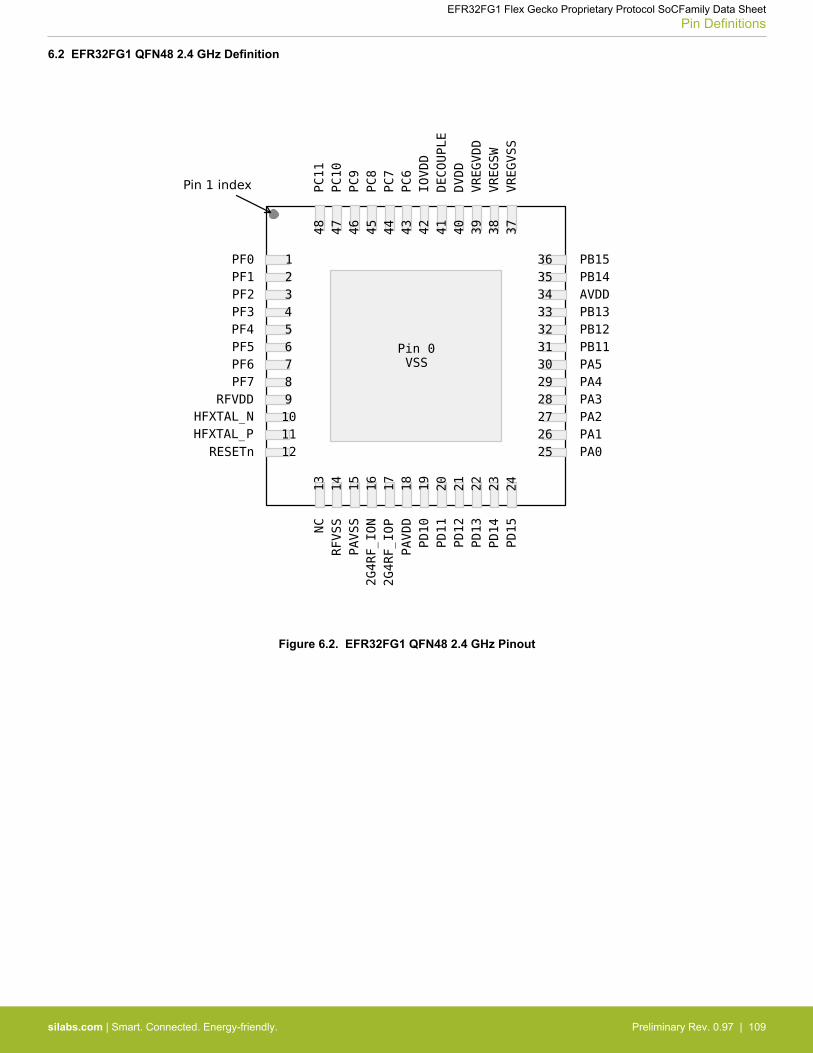
6.2 EFR32FG1 QFN48 2.4 GHz Definition
Figure 6.2. EFR32FG1 QFN48 2.4 GHz Pinout
EFR32FG1 Flex Gecko Proprietary Protocol SoCFamily Data SheetPin Definitions
silabs.com | Smart. Connected. Energy-friendly. Preliminary Rev. 0.97 | 109

Table 6.3. QFN48 2.4 GHz Device Pinout
QFN48 Pin# andName
Pin Alternate Functionality / Description
Pin# Pin Name Analog Timers Communication Radio Other
0 VSS Ground
1 PF0
BUSAX [ADC0:APORT1XCH16
ACMP0:APORT1XCH16
ACMP1:APORT1XCH16]
BUSBY [ADC0:APORT2YCH16
ACMP0:APORT2YCH16
ACMP1:APORT2YCH16]
TIM0_CC0 #24TIM0_CC1 #23TIM0_CC2 #22
TIM0_CDTI0 #21TIM0_CDTI1 #20TIM0_CDTI2 #19TIM1_CC0 #24TIM1_CC1 #23TIM1_CC2 #22
TIM1_CC3 #21 LE-TIM0_OUT0 #24
LETIM0_OUT1 #23PCNT0_S0IN #24PCNT0_S1IN #23
US0_TX #24US0_RX #23
US0_CLK #22US0_CS #21
US0_CTS #20US0_RTS #19US1_TX #24US1_RX #23
US1_CLK #22US1_CS #21
US1_CTS #20US1_RTS #19LEU0_TX #24LEU0_RX #23I2C0_SDA #24I2C0_SCL #23
FRC_DCLK #24FRC_DOUT #23
FRC_DFRAME #22MODEM_DCLK #24MODEM_DIN #23
MODEM_DOUT #22MODEM_ANT0 #21MODEM_ANT1 #20
PRS_CH0 #0PRS_CH1 #7PRS_CH2 #6PRS_CH3 #5
ACMP0_O #24ACMP1_O #24
DBG_SWCLKTCK#0
2 PF1
BUSAY [ADC0:APORT1YCH17
ACMP0:APORT1YCH17
ACMP1:APORT1YCH17]
BUSBX [ADC0:APORT2XCH17
ACMP0:APORT2XCH17
ACMP1:APORT2XCH17]
TIM0_CC0 #25TIM0_CC1 #24TIM0_CC2 #23
TIM0_CDTI0 #22TIM0_CDTI1 #21TIM0_CDTI2 #20TIM1_CC0 #25TIM1_CC1 #24TIM1_CC2 #23
TIM1_CC3 #22 LE-TIM0_OUT0 #25
LETIM0_OUT1 #24PCNT0_S0IN #25PCNT0_S1IN #24
US0_TX #25US0_RX #24
US0_CLK #23US0_CS #22
US0_CTS #21US0_RTS #20US1_TX #25US1_RX #24
US1_CLK #23US1_CS #22
US1_CTS #21US1_RTS #20LEU0_TX #25LEU0_RX #24I2C0_SDA #25I2C0_SCL #24
FRC_DCLK #25FRC_DOUT #24
FRC_DFRAME #23MODEM_DCLK #25MODEM_DIN #24
MODEM_DOUT #23MODEM_ANT0 #22MODEM_ANT1 #21
PRS_CH0 #1PRS_CH1 #0PRS_CH2 #7PRS_CH3 #6
ACMP0_O #25ACMP1_O #25
DBG_SWDIOTMS#0
3 PF2
BUSAX [ADC0:APORT1XCH18
ACMP0:APORT1XCH18
ACMP1:APORT1XCH18]
BUSBY [ADC0:APORT2YCH18
ACMP0:APORT2YCH18
ACMP1:APORT2YCH18]
TIM0_CC0 #26TIM0_CC1 #25TIM0_CC2 #24
TIM0_CDTI0 #23TIM0_CDTI1 #22TIM0_CDTI2 #21TIM1_CC0 #26TIM1_CC1 #25TIM1_CC2 #24
TIM1_CC3 #23 LE-TIM0_OUT0 #26
LETIM0_OUT1 #25PCNT0_S0IN #26PCNT0_S1IN #25
US0_TX #26US0_RX #25
US0_CLK #24US0_CS #23
US0_CTS #22US0_RTS #21US1_TX #26US1_RX #25
US1_CLK #24US1_CS #23
US1_CTS #22US1_RTS #21LEU0_TX #26LEU0_RX #25I2C0_SDA #26I2C0_SCL #25
FRC_DCLK #26FRC_DOUT #25
FRC_DFRAME #24MODEM_DCLK #26MODEM_DIN #25
MODEM_DOUT #24MODEM_ANT0 #23MODEM_ANT1 #22
CMU_CLK0 #6PRS_CH0 #2PRS_CH1 #1PRS_CH2 #0PRS_CH3 #7
ACMP0_O #26ACMP1_O #26DBG_TDO #0DBG_SWO #0
GPIO_EM4WU0
EFR32FG1 Flex Gecko Proprietary Protocol SoCFamily Data SheetPin Definitions
silabs.com | Smart. Connected. Energy-friendly. Preliminary Rev. 0.97 | 110

QFN48 Pin# andName
Pin Alternate Functionality / Description
Pin# Pin Name Analog Timers Communication Radio Other
4 PF3
BUSAY [ADC0:APORT1YCH19
ACMP0:APORT1YCH19
ACMP1:APORT1YCH19]
BUSBX [ADC0:APORT2XCH19
ACMP0:APORT2XCH19
ACMP1:APORT2XCH19]
TIM0_CC0 #27TIM0_CC1 #26TIM0_CC2 #25
TIM0_CDTI0 #24TIM0_CDTI1 #23TIM0_CDTI2 #22TIM1_CC0 #27TIM1_CC1 #26TIM1_CC2 #25
TIM1_CC3 #24 LE-TIM0_OUT0 #27
LETIM0_OUT1 #26PCNT0_S0IN #27PCNT0_S1IN #26
US0_TX #27US0_RX #26
US0_CLK #25US0_CS #24
US0_CTS #23US0_RTS #22US1_TX #27US1_RX #26
US1_CLK #25US1_CS #24
US1_CTS #23US1_RTS #22LEU0_TX #27LEU0_RX #26I2C0_SDA #27I2C0_SCL #26
FRC_DCLK #27FRC_DOUT #26
FRC_DFRAME #25MODEM_DCLK #27MODEM_DIN #26
MODEM_DOUT #25MODEM_ANT0 #24MODEM_ANT1 #23
CMU_CLK1 #6PRS_CH0 #3PRS_CH1 #2PRS_CH2 #1PRS_CH3 #0
ACMP0_O #27ACMP1_O #27DBG_TDI #0
5 PF4
BUSAX [ADC0:APORT1XCH20
ACMP0:APORT1XCH20
ACMP1:APORT1XCH20]
BUSBY [ADC0:APORT2YCH20
ACMP0:APORT2YCH20
ACMP1:APORT2YCH20]
TIM0_CC0 #28TIM0_CC1 #27TIM0_CC2 #26
TIM0_CDTI0 #25TIM0_CDTI1 #24TIM0_CDTI2 #23TIM1_CC0 #28TIM1_CC1 #27TIM1_CC2 #26
TIM1_CC3 #25 LE-TIM0_OUT0 #28
LETIM0_OUT1 #27PCNT0_S0IN #28PCNT0_S1IN #27
US0_TX #28US0_RX #27
US0_CLK #26US0_CS #25
US0_CTS #24US0_RTS #23US1_TX #28US1_RX #27
US1_CLK #26US1_CS #25
US1_CTS #24US1_RTS #23LEU0_TX #28LEU0_RX #27I2C0_SDA #28I2C0_SCL #27
FRC_DCLK #28FRC_DOUT #27
FRC_DFRAME #26MODEM_DCLK #28MODEM_DIN #27
MODEM_DOUT #26MODEM_ANT0 #25MODEM_ANT1 #24
PRS_CH0 #4PRS_CH1 #3PRS_CH2 #2PRS_CH3 #1
ACMP0_O #28ACMP1_O #28
6 PF5
BUSAY [ADC0:APORT1YCH21
ACMP0:APORT1YCH21
ACMP1:APORT1YCH21]
BUSBX [ADC0:APORT2XCH21
ACMP0:APORT2XCH21
ACMP1:APORT2XCH21]
TIM0_CC0 #29TIM0_CC1 #28TIM0_CC2 #27
TIM0_CDTI0 #26TIM0_CDTI1 #25TIM0_CDTI2 #24TIM1_CC0 #29TIM1_CC1 #28TIM1_CC2 #27
TIM1_CC3 #26 LE-TIM0_OUT0 #29
LETIM0_OUT1 #28PCNT0_S0IN #29PCNT0_S1IN #28
US0_TX #29US0_RX #28
US0_CLK #27US0_CS #26
US0_CTS #25US0_RTS #24US1_TX #29US1_RX #28
US1_CLK #27US1_CS #26
US1_CTS #25US1_RTS #24LEU0_TX #29LEU0_RX #28I2C0_SDA #29I2C0_SCL #28
FRC_DCLK #29FRC_DOUT #28
FRC_DFRAME #27MODEM_DCLK #29MODEM_DIN #28
MODEM_DOUT #27MODEM_ANT0 #26MODEM_ANT1 #25
PRS_CH0 #5PRS_CH1 #4PRS_CH2 #3PRS_CH3 #2
ACMP0_O #29ACMP1_O #29
EFR32FG1 Flex Gecko Proprietary Protocol SoCFamily Data SheetPin Definitions
silabs.com | Smart. Connected. Energy-friendly. Preliminary Rev. 0.97 | 111
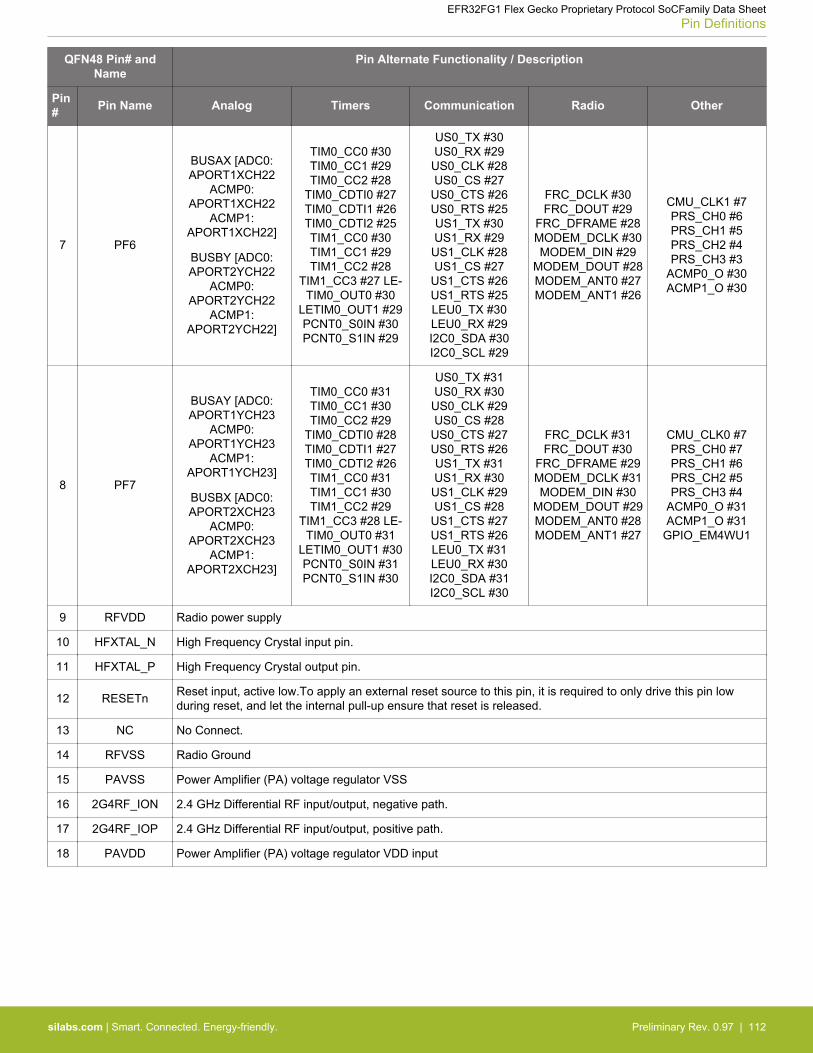
QFN48 Pin# andName
Pin Alternate Functionality / Description
Pin# Pin Name Analog Timers Communication Radio Other
7 PF6
BUSAX [ADC0:APORT1XCH22
ACMP0:APORT1XCH22
ACMP1:APORT1XCH22]
BUSBY [ADC0:APORT2YCH22
ACMP0:APORT2YCH22
ACMP1:APORT2YCH22]
TIM0_CC0 #30TIM0_CC1 #29TIM0_CC2 #28
TIM0_CDTI0 #27TIM0_CDTI1 #26TIM0_CDTI2 #25TIM1_CC0 #30TIM1_CC1 #29TIM1_CC2 #28
TIM1_CC3 #27 LE-TIM0_OUT0 #30
LETIM0_OUT1 #29PCNT0_S0IN #30PCNT0_S1IN #29
US0_TX #30US0_RX #29
US0_CLK #28US0_CS #27
US0_CTS #26US0_RTS #25US1_TX #30US1_RX #29
US1_CLK #28US1_CS #27
US1_CTS #26US1_RTS #25LEU0_TX #30LEU0_RX #29I2C0_SDA #30I2C0_SCL #29
FRC_DCLK #30FRC_DOUT #29
FRC_DFRAME #28MODEM_DCLK #30MODEM_DIN #29
MODEM_DOUT #28MODEM_ANT0 #27MODEM_ANT1 #26
CMU_CLK1 #7PRS_CH0 #6PRS_CH1 #5PRS_CH2 #4PRS_CH3 #3
ACMP0_O #30ACMP1_O #30
8 PF7
BUSAY [ADC0:APORT1YCH23
ACMP0:APORT1YCH23
ACMP1:APORT1YCH23]
BUSBX [ADC0:APORT2XCH23
ACMP0:APORT2XCH23
ACMP1:APORT2XCH23]
TIM0_CC0 #31TIM0_CC1 #30TIM0_CC2 #29
TIM0_CDTI0 #28TIM0_CDTI1 #27TIM0_CDTI2 #26TIM1_CC0 #31TIM1_CC1 #30TIM1_CC2 #29
TIM1_CC3 #28 LE-TIM0_OUT0 #31
LETIM0_OUT1 #30PCNT0_S0IN #31PCNT0_S1IN #30
US0_TX #31US0_RX #30
US0_CLK #29US0_CS #28
US0_CTS #27US0_RTS #26US1_TX #31US1_RX #30
US1_CLK #29US1_CS #28
US1_CTS #27US1_RTS #26LEU0_TX #31LEU0_RX #30I2C0_SDA #31I2C0_SCL #30
FRC_DCLK #31FRC_DOUT #30
FRC_DFRAME #29MODEM_DCLK #31MODEM_DIN #30
MODEM_DOUT #29MODEM_ANT0 #28MODEM_ANT1 #27
CMU_CLK0 #7PRS_CH0 #7PRS_CH1 #6PRS_CH2 #5PRS_CH3 #4
ACMP0_O #31ACMP1_O #31
GPIO_EM4WU1
9 RFVDD Radio power supply
10 HFXTAL_N High Frequency Crystal input pin.
11 HFXTAL_P High Frequency Crystal output pin.
12 RESETn Reset input, active low.To apply an external reset source to this pin, it is required to only drive this pin lowduring reset, and let the internal pull-up ensure that reset is released.
13 NC No Connect.
14 RFVSS Radio Ground
15 PAVSS Power Amplifier (PA) voltage regulator VSS
16 2G4RF_ION 2.4 GHz Differential RF input/output, negative path.
17 2G4RF_IOP 2.4 GHz Differential RF input/output, positive path.
18 PAVDD Power Amplifier (PA) voltage regulator VDD input
EFR32FG1 Flex Gecko Proprietary Protocol SoCFamily Data SheetPin Definitions
silabs.com | Smart. Connected. Energy-friendly. Preliminary Rev. 0.97 | 112
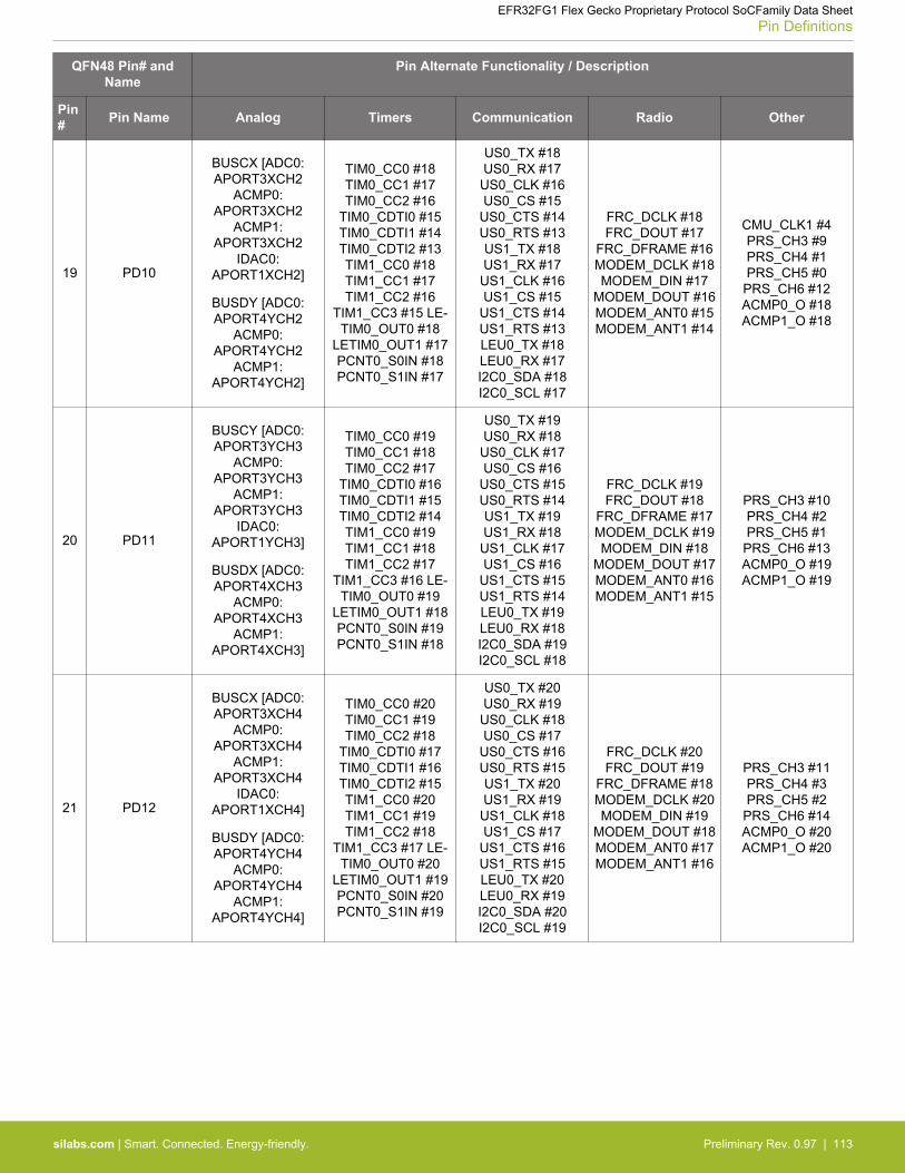
QFN48 Pin# andName
Pin Alternate Functionality / Description
Pin# Pin Name Analog Timers Communication Radio Other
19 PD10
BUSCX [ADC0:APORT3XCH2
ACMP0:APORT3XCH2
ACMP1:APORT3XCH2
IDAC0:APORT1XCH2]
BUSDY [ADC0:APORT4YCH2
ACMP0:APORT4YCH2
ACMP1:APORT4YCH2]
TIM0_CC0 #18TIM0_CC1 #17TIM0_CC2 #16
TIM0_CDTI0 #15TIM0_CDTI1 #14TIM0_CDTI2 #13TIM1_CC0 #18TIM1_CC1 #17TIM1_CC2 #16
TIM1_CC3 #15 LE-TIM0_OUT0 #18
LETIM0_OUT1 #17PCNT0_S0IN #18PCNT0_S1IN #17
US0_TX #18US0_RX #17
US0_CLK #16US0_CS #15
US0_CTS #14US0_RTS #13US1_TX #18US1_RX #17
US1_CLK #16US1_CS #15
US1_CTS #14US1_RTS #13LEU0_TX #18LEU0_RX #17I2C0_SDA #18I2C0_SCL #17
FRC_DCLK #18FRC_DOUT #17
FRC_DFRAME #16MODEM_DCLK #18MODEM_DIN #17
MODEM_DOUT #16MODEM_ANT0 #15MODEM_ANT1 #14
CMU_CLK1 #4PRS_CH3 #9PRS_CH4 #1PRS_CH5 #0
PRS_CH6 #12ACMP0_O #18ACMP1_O #18
20 PD11
BUSCY [ADC0:APORT3YCH3
ACMP0:APORT3YCH3
ACMP1:APORT3YCH3
IDAC0:APORT1YCH3]
BUSDX [ADC0:APORT4XCH3
ACMP0:APORT4XCH3
ACMP1:APORT4XCH3]
TIM0_CC0 #19TIM0_CC1 #18TIM0_CC2 #17
TIM0_CDTI0 #16TIM0_CDTI1 #15TIM0_CDTI2 #14TIM1_CC0 #19TIM1_CC1 #18TIM1_CC2 #17
TIM1_CC3 #16 LE-TIM0_OUT0 #19
LETIM0_OUT1 #18PCNT0_S0IN #19PCNT0_S1IN #18
US0_TX #19US0_RX #18
US0_CLK #17US0_CS #16
US0_CTS #15US0_RTS #14US1_TX #19US1_RX #18
US1_CLK #17US1_CS #16
US1_CTS #15US1_RTS #14LEU0_TX #19LEU0_RX #18I2C0_SDA #19I2C0_SCL #18
FRC_DCLK #19FRC_DOUT #18
FRC_DFRAME #17MODEM_DCLK #19MODEM_DIN #18
MODEM_DOUT #17MODEM_ANT0 #16MODEM_ANT1 #15
PRS_CH3 #10PRS_CH4 #2PRS_CH5 #1
PRS_CH6 #13ACMP0_O #19ACMP1_O #19
21 PD12
BUSCX [ADC0:APORT3XCH4
ACMP0:APORT3XCH4
ACMP1:APORT3XCH4
IDAC0:APORT1XCH4]
BUSDY [ADC0:APORT4YCH4
ACMP0:APORT4YCH4
ACMP1:APORT4YCH4]
TIM0_CC0 #20TIM0_CC1 #19TIM0_CC2 #18
TIM0_CDTI0 #17TIM0_CDTI1 #16TIM0_CDTI2 #15TIM1_CC0 #20TIM1_CC1 #19TIM1_CC2 #18
TIM1_CC3 #17 LE-TIM0_OUT0 #20
LETIM0_OUT1 #19PCNT0_S0IN #20PCNT0_S1IN #19
US0_TX #20US0_RX #19
US0_CLK #18US0_CS #17
US0_CTS #16US0_RTS #15US1_TX #20US1_RX #19
US1_CLK #18US1_CS #17
US1_CTS #16US1_RTS #15LEU0_TX #20LEU0_RX #19I2C0_SDA #20I2C0_SCL #19
FRC_DCLK #20FRC_DOUT #19
FRC_DFRAME #18MODEM_DCLK #20MODEM_DIN #19
MODEM_DOUT #18MODEM_ANT0 #17MODEM_ANT1 #16
PRS_CH3 #11PRS_CH4 #3PRS_CH5 #2
PRS_CH6 #14ACMP0_O #20ACMP1_O #20
EFR32FG1 Flex Gecko Proprietary Protocol SoCFamily Data SheetPin Definitions
silabs.com | Smart. Connected. Energy-friendly. Preliminary Rev. 0.97 | 113

QFN48 Pin# andName
Pin Alternate Functionality / Description
Pin# Pin Name Analog Timers Communication Radio Other
22 PD13
BUSCY [ADC0:APORT3YCH5
ACMP0:APORT3YCH5
ACMP1:APORT3YCH5
IDAC0:APORT1YCH5]
BUSDX [ADC0:APORT4XCH5
ACMP0:APORT4XCH5
ACMP1:APORT4XCH5]
TIM0_CC0 #21TIM0_CC1 #20TIM0_CC2 #19
TIM0_CDTI0 #18TIM0_CDTI1 #17TIM0_CDTI2 #16TIM1_CC0 #21TIM1_CC1 #20TIM1_CC2 #19
TIM1_CC3 #18 LE-TIM0_OUT0 #21
LETIM0_OUT1 #20PCNT0_S0IN #21PCNT0_S1IN #20
US0_TX #21US0_RX #20
US0_CLK #19US0_CS #18
US0_CTS #17US0_RTS #16US1_TX #21US1_RX #20
US1_CLK #19US1_CS #18
US1_CTS #17US1_RTS #16LEU0_TX #21LEU0_RX #20I2C0_SDA #21I2C0_SCL #20
FRC_DCLK #21FRC_DOUT #20
FRC_DFRAME #19MODEM_DCLK #21MODEM_DIN #20
MODEM_DOUT #19MODEM_ANT0 #18MODEM_ANT1 #17
PRS_CH3 #12PRS_CH4 #4PRS_CH5 #3
PRS_CH6 #15ACMP0_O #21ACMP1_O #21
23 PD14
BUSCX [ADC0:APORT3XCH6
ACMP0:APORT3XCH6
ACMP1:APORT3XCH6
IDAC0:APORT1XCH6]
BUSDY [ADC0:APORT4YCH6
ACMP0:APORT4YCH6
ACMP1:APORT4YCH6]
TIM0_CC0 #22TIM0_CC1 #21TIM0_CC2 #20
TIM0_CDTI0 #19TIM0_CDTI1 #18TIM0_CDTI2 #17TIM1_CC0 #22TIM1_CC1 #21TIM1_CC2 #20
TIM1_CC3 #19 LE-TIM0_OUT0 #22
LETIM0_OUT1 #21PCNT0_S0IN #22PCNT0_S1IN #21
US0_TX #22US0_RX #21
US0_CLK #20US0_CS #19
US0_CTS #18US0_RTS #17US1_TX #22US1_RX #21
US1_CLK #20US1_CS #19
US1_CTS #18US1_RTS #17LEU0_TX #22LEU0_RX #21I2C0_SDA #22I2C0_SCL #21
FRC_DCLK #22FRC_DOUT #21
FRC_DFRAME #20MODEM_DCLK #22MODEM_DIN #21
MODEM_DOUT #20MODEM_ANT0 #19MODEM_ANT1 #18
CMU_CLK0 #5PRS_CH3 #13PRS_CH4 #5PRS_CH5 #4
PRS_CH6 #16ACMP0_O #22ACMP1_O #22
GPIO_EM4WU4
24 PD15
BUSCY [ADC0:APORT3YCH7
ACMP0:APORT3YCH7
ACMP1:APORT3YCH7
IDAC0:APORT1YCH7]
BUSDX [ADC0:APORT4XCH7
ACMP0:APORT4XCH7
ACMP1:APORT4XCH7]
TIM0_CC0 #23TIM0_CC1 #22TIM0_CC2 #21
TIM0_CDTI0 #20TIM0_CDTI1 #19TIM0_CDTI2 #18TIM1_CC0 #23TIM1_CC1 #22TIM1_CC2 #21
TIM1_CC3 #20 LE-TIM0_OUT0 #23
LETIM0_OUT1 #22PCNT0_S0IN #23PCNT0_S1IN #22
US0_TX #23US0_RX #22
US0_CLK #21US0_CS #20
US0_CTS #19US0_RTS #18US1_TX #23US1_RX #22
US1_CLK #21US1_CS #20
US1_CTS #19US1_RTS #18LEU0_TX #23LEU0_RX #22I2C0_SDA #23I2C0_SCL #22
FRC_DCLK #23FRC_DOUT #22
FRC_DFRAME #21MODEM_DCLK #23MODEM_DIN #22
MODEM_DOUT #21MODEM_ANT0 #20MODEM_ANT1 #19
CMU_CLK1 #5PRS_CH3 #14PRS_CH4 #6PRS_CH5 #5
PRS_CH6 #17ACMP0_O #23ACMP1_O #23DBG_SWO #2
EFR32FG1 Flex Gecko Proprietary Protocol SoCFamily Data SheetPin Definitions
silabs.com | Smart. Connected. Energy-friendly. Preliminary Rev. 0.97 | 114

QFN48 Pin# andName
Pin Alternate Functionality / Description
Pin# Pin Name Analog Timers Communication Radio Other
25 PA0
ADC0_EXTN
BUSCX [ADC0:APORT3XCH8
ACMP0:APORT3XCH8
ACMP1:APORT3XCH8
IDAC0:APORT1XCH8]
BUSDY [ADC0:APORT4YCH8
ACMP0:APORT4YCH8
ACMP1:APORT4YCH8]
TIM0_CC0 #0TIM0_CC1 #31TIM0_CC2 #30
TIM0_CDTI0 #29TIM0_CDTI1 #28TIM0_CDTI2 #27
TIM1_CC0 #0TIM1_CC1 #31TIM1_CC2 #30
TIM1_CC3 #29 LE-TIM0_OUT0 #0 LE-
TIM0_OUT1 #31PCNT0_S0IN #0PCNT0_S1IN #31
US0_TX #0US0_RX #31
US0_CLK #30US0_CS #29
US0_CTS #28US0_RTS #27
US1_TX #0US1_RX #31
US1_CLK #30US1_CS #29
US1_CTS #28US1_RTS #27LEU0_TX #0
LEU0_RX #31I2C0_SDA #0I2C0_SCL #31
FRC_DCLK #0FRC_DOUT #31
FRC_DFRAME #30MODEM_DCLK #0MODEM_DIN #31
MODEM_DOUT #30MODEM_ANT0 #29MODEM_ANT1 #28
CMU_CLK1 #0PRS_CH6 #0
PRS_CH7 #10PRS_CH8 #9PRS_CH9 #8ACMP0_O #0ACMP1_O #0
26 PA1
ADC0_EXTP
BUSCY [ADC0:APORT3YCH9
ACMP0:APORT3YCH9
ACMP1:APORT3YCH9
IDAC0:APORT1YCH9]
BUSDX [ADC0:APORT4XCH9
ACMP0:APORT4XCH9
ACMP1:APORT4XCH9]
TIM0_CC0 #1TIM0_CC1 #0TIM0_CC2 #31
TIM0_CDTI0 #30TIM0_CDTI1 #29TIM0_CDTI2 #28
TIM1_CC0 #1TIM1_CC1 #0TIM1_CC2 #31
TIM1_CC3 #30 LE-TIM0_OUT0 #1 LE-
TIM0_OUT1 #0PCNT0_S0IN #1PCNT0_S1IN #0
US0_TX #1US0_RX #0
US0_CLK #31US0_CS #30
US0_CTS #29US0_RTS #28
US1_TX #1US1_RX #0
US1_CLK #31US1_CS #30
US1_CTS #29US1_RTS #28LEU0_TX #1LEU0_RX #0I2C0_SDA #1I2C0_SCL #0
FRC_DCLK #1FRC_DOUT #0
FRC_DFRAME #31MODEM_DCLK #1MODEM_DIN #0
MODEM_DOUT #31MODEM_ANT0 #30MODEM_ANT1 #29
CMU_CLK0 #0PRS_CH6 #1PRS_CH7 #0
PRS_CH8 #10PRS_CH9 #9ACMP0_O #1ACMP1_O #1
27 PA2
BUSCX [ADC0:APORT3XCH10
ACMP0:APORT3XCH10
ACMP1:APORT3XCH10
IDAC0:APORT1XCH10]
BUSDY [ADC0:APORT4YCH10
ACMP0:APORT4YCH10
ACMP1:APORT4YCH10]
TIM0_CC0 #2TIM0_CC1 #1TIM0_CC2 #0
TIM0_CDTI0 #31TIM0_CDTI1 #30TIM0_CDTI2 #29
TIM1_CC0 #2TIM1_CC1 #1TIM1_CC2 #0
TIM1_CC3 #31 LE-TIM0_OUT0 #2 LE-
TIM0_OUT1 #1PCNT0_S0IN #2PCNT0_S1IN #1
US0_TX #2US0_RX #1
US0_CLK #0US0_CS #31
US0_CTS #30US0_RTS #29
US1_TX #2US1_RX #1
US1_CLK #0US1_CS #31
US1_CTS #30US1_RTS #29LEU0_TX #2LEU0_RX #1I2C0_SDA #2I2C0_SCL #1
FRC_DCLK #2FRC_DOUT #1
FRC_DFRAME #0MODEM_DCLK #2MODEM_DIN #1
MODEM_DOUT #0MODEM_ANT0 #31MODEM_ANT1 #30
PRS_CH6 #2PRS_CH7 #1PRS_CH8 #0
PRS_CH9 #10ACMP0_O #2ACMP1_O #2
EFR32FG1 Flex Gecko Proprietary Protocol SoCFamily Data SheetPin Definitions
silabs.com | Smart. Connected. Energy-friendly. Preliminary Rev. 0.97 | 115

QFN48 Pin# andName
Pin Alternate Functionality / Description
Pin# Pin Name Analog Timers Communication Radio Other
28 PA3
BUSCY [ADC0:APORT3YCH11
ACMP0:APORT3YCH11
ACMP1:APORT3YCH11
IDAC0:APORT1YCH11]
BUSDX [ADC0:APORT4XCH11
ACMP0:APORT4XCH11
ACMP1:APORT4XCH11]
TIM0_CC0 #3TIM0_CC1 #2TIM0_CC2 #1
TIM0_CDTI0 #0TIM0_CDTI1 #31TIM0_CDTI2 #30
TIM1_CC0 #3TIM1_CC1 #2TIM1_CC2 #1
TIM1_CC3 #0 LE-TIM0_OUT0 #3 LE-
TIM0_OUT1 #2PCNT0_S0IN #3PCNT0_S1IN #2
US0_TX #3US0_RX #2
US0_CLK #1US0_CS #0
US0_CTS #31US0_RTS #30
US1_TX #3US1_RX #2
US1_CLK #1US1_CS #0
US1_CTS #31US1_RTS #30LEU0_TX #3LEU0_RX #2I2C0_SDA #3I2C0_SCL #2
FRC_DCLK #3FRC_DOUT #2
FRC_DFRAME #1MODEM_DCLK #3MODEM_DIN #2
MODEM_DOUT #1MODEM_ANT0 #0
MODEM_ANT1 #31
PRS_CH6 #3PRS_CH7 #2PRS_CH8 #1PRS_CH9 #0ACMP0_O #3ACMP1_O #3
GPIO_EM4WU8
29 PA4
BUSCX [ADC0:APORT3XCH12
ACMP0:APORT3XCH12
ACMP1:APORT3XCH12
IDAC0:APORT1XCH12]
BUSDY [ADC0:APORT4YCH12
ACMP0:APORT4YCH12
ACMP1:APORT4YCH12]
TIM0_CC0 #4TIM0_CC1 #3TIM0_CC2 #2
TIM0_CDTI0 #1TIM0_CDTI1 #0TIM0_CDTI2 #31
TIM1_CC0 #4TIM1_CC1 #3TIM1_CC2 #2
TIM1_CC3 #1 LE-TIM0_OUT0 #4 LE-
TIM0_OUT1 #3PCNT0_S0IN #4PCNT0_S1IN #3
US0_TX #4US0_RX #3
US0_CLK #2US0_CS #1
US0_CTS #0US0_RTS #31
US1_TX #4US1_RX #3
US1_CLK #2US1_CS #1
US1_CTS #0US1_RTS #31LEU0_TX #4LEU0_RX #3I2C0_SDA #4I2C0_SCL #3
FRC_DCLK #4FRC_DOUT #3
FRC_DFRAME #2MODEM_DCLK #4MODEM_DIN #3
MODEM_DOUT #2MODEM_ANT0 #1MODEM_ANT1 #0
PRS_CH6 #4PRS_CH7 #3PRS_CH8 #2PRS_CH9 #1ACMP0_O #4ACMP1_O #4
30 PA5
BUSCY [ADC0:APORT3YCH13
ACMP0:APORT3YCH13
ACMP1:APORT3YCH13
IDAC0:APORT1YCH13]
BUSDX [ADC0:APORT4XCH13
ACMP0:APORT4XCH13
ACMP1:APORT4XCH13]
TIM0_CC0 #5TIM0_CC1 #4TIM0_CC2 #3
TIM0_CDTI0 #2TIM0_CDTI1 #1TIM0_CDTI2 #0TIM1_CC0 #5TIM1_CC1 #4TIM1_CC2 #3
TIM1_CC3 #2 LE-TIM0_OUT0 #5 LE-
TIM0_OUT1 #4PCNT0_S0IN #5PCNT0_S1IN #4
US0_TX #5US0_RX #4
US0_CLK #3US0_CS #2
US0_CTS #1US0_RTS #0US1_TX #5US1_RX #4
US1_CLK #3US1_CS #2
US1_CTS #1US1_RTS #0LEU0_TX #5LEU0_RX #4I2C0_SDA #5I2C0_SCL #4
FRC_DCLK #5FRC_DOUT #4
FRC_DFRAME #3MODEM_DCLK #5MODEM_DIN #4
MODEM_DOUT #3MODEM_ANT0 #2MODEM_ANT1 #1
PRS_CH6 #5PRS_CH7 #4PRS_CH8 #3PRS_CH9 #2ACMP0_O #5ACMP1_O #5
EFR32FG1 Flex Gecko Proprietary Protocol SoCFamily Data SheetPin Definitions
silabs.com | Smart. Connected. Energy-friendly. Preliminary Rev. 0.97 | 116
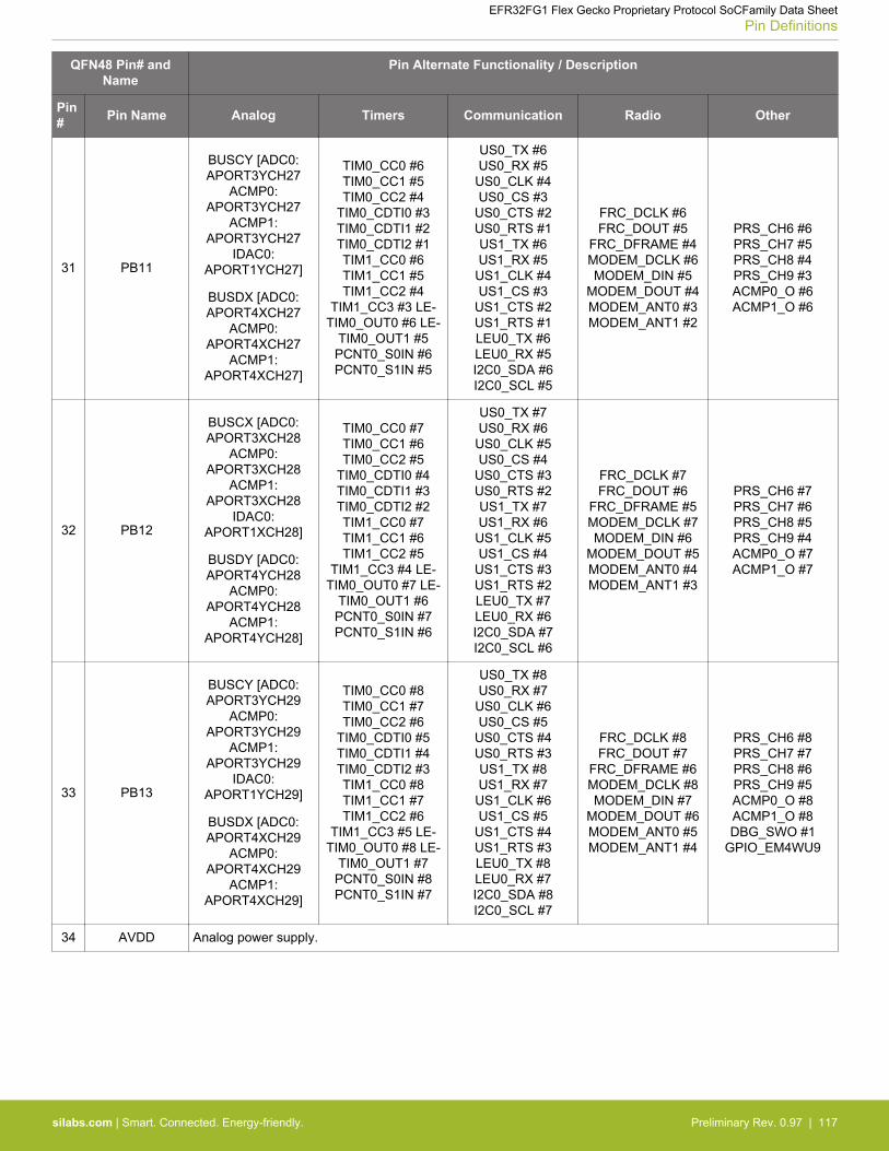
QFN48 Pin# andName
Pin Alternate Functionality / Description
Pin# Pin Name Analog Timers Communication Radio Other
31 PB11
BUSCY [ADC0:APORT3YCH27
ACMP0:APORT3YCH27
ACMP1:APORT3YCH27
IDAC0:APORT1YCH27]
BUSDX [ADC0:APORT4XCH27
ACMP0:APORT4XCH27
ACMP1:APORT4XCH27]
TIM0_CC0 #6TIM0_CC1 #5TIM0_CC2 #4
TIM0_CDTI0 #3TIM0_CDTI1 #2TIM0_CDTI2 #1TIM1_CC0 #6TIM1_CC1 #5TIM1_CC2 #4
TIM1_CC3 #3 LE-TIM0_OUT0 #6 LE-
TIM0_OUT1 #5PCNT0_S0IN #6PCNT0_S1IN #5
US0_TX #6US0_RX #5
US0_CLK #4US0_CS #3
US0_CTS #2US0_RTS #1US1_TX #6US1_RX #5
US1_CLK #4US1_CS #3
US1_CTS #2US1_RTS #1LEU0_TX #6LEU0_RX #5I2C0_SDA #6I2C0_SCL #5
FRC_DCLK #6FRC_DOUT #5
FRC_DFRAME #4MODEM_DCLK #6MODEM_DIN #5
MODEM_DOUT #4MODEM_ANT0 #3MODEM_ANT1 #2
PRS_CH6 #6PRS_CH7 #5PRS_CH8 #4PRS_CH9 #3ACMP0_O #6ACMP1_O #6
32 PB12
BUSCX [ADC0:APORT3XCH28
ACMP0:APORT3XCH28
ACMP1:APORT3XCH28
IDAC0:APORT1XCH28]
BUSDY [ADC0:APORT4YCH28
ACMP0:APORT4YCH28
ACMP1:APORT4YCH28]
TIM0_CC0 #7TIM0_CC1 #6TIM0_CC2 #5
TIM0_CDTI0 #4TIM0_CDTI1 #3TIM0_CDTI2 #2TIM1_CC0 #7TIM1_CC1 #6TIM1_CC2 #5
TIM1_CC3 #4 LE-TIM0_OUT0 #7 LE-
TIM0_OUT1 #6PCNT0_S0IN #7PCNT0_S1IN #6
US0_TX #7US0_RX #6
US0_CLK #5US0_CS #4
US0_CTS #3US0_RTS #2US1_TX #7US1_RX #6
US1_CLK #5US1_CS #4
US1_CTS #3US1_RTS #2LEU0_TX #7LEU0_RX #6I2C0_SDA #7I2C0_SCL #6
FRC_DCLK #7FRC_DOUT #6
FRC_DFRAME #5MODEM_DCLK #7MODEM_DIN #6
MODEM_DOUT #5MODEM_ANT0 #4MODEM_ANT1 #3
PRS_CH6 #7PRS_CH7 #6PRS_CH8 #5PRS_CH9 #4ACMP0_O #7ACMP1_O #7
33 PB13
BUSCY [ADC0:APORT3YCH29
ACMP0:APORT3YCH29
ACMP1:APORT3YCH29
IDAC0:APORT1YCH29]
BUSDX [ADC0:APORT4XCH29
ACMP0:APORT4XCH29
ACMP1:APORT4XCH29]
TIM0_CC0 #8TIM0_CC1 #7TIM0_CC2 #6
TIM0_CDTI0 #5TIM0_CDTI1 #4TIM0_CDTI2 #3TIM1_CC0 #8TIM1_CC1 #7TIM1_CC2 #6
TIM1_CC3 #5 LE-TIM0_OUT0 #8 LE-
TIM0_OUT1 #7PCNT0_S0IN #8PCNT0_S1IN #7
US0_TX #8US0_RX #7
US0_CLK #6US0_CS #5
US0_CTS #4US0_RTS #3US1_TX #8US1_RX #7
US1_CLK #6US1_CS #5
US1_CTS #4US1_RTS #3LEU0_TX #8LEU0_RX #7I2C0_SDA #8I2C0_SCL #7
FRC_DCLK #8FRC_DOUT #7
FRC_DFRAME #6MODEM_DCLK #8MODEM_DIN #7
MODEM_DOUT #6MODEM_ANT0 #5MODEM_ANT1 #4
PRS_CH6 #8PRS_CH7 #7PRS_CH8 #6PRS_CH9 #5ACMP0_O #8ACMP1_O #8DBG_SWO #1
GPIO_EM4WU9
34 AVDD Analog power supply.
EFR32FG1 Flex Gecko Proprietary Protocol SoCFamily Data SheetPin Definitions
silabs.com | Smart. Connected. Energy-friendly. Preliminary Rev. 0.97 | 117

QFN48 Pin# andName
Pin Alternate Functionality / Description
Pin# Pin Name Analog Timers Communication Radio Other
35 PB14
LFXTAL_N
BUSCX [ADC0:APORT3XCH30
ACMP0:APORT3XCH30
ACMP1:APORT3XCH30
IDAC0:APORT1XCH30]
BUSDY [ADC0:APORT4YCH30
ACMP0:APORT4YCH30
ACMP1:APORT4YCH30]
TIM0_CC0 #9TIM0_CC1 #8TIM0_CC2 #7
TIM0_CDTI0 #6TIM0_CDTI1 #5TIM0_CDTI2 #4TIM1_CC0 #9TIM1_CC1 #8TIM1_CC2 #7
TIM1_CC3 #6 LE-TIM0_OUT0 #9 LE-
TIM0_OUT1 #8PCNT0_S0IN #9PCNT0_S1IN #8
US0_TX #9US0_RX #8
US0_CLK #7US0_CS #6
US0_CTS #5US0_RTS #4US1_TX #9US1_RX #8
US1_CLK #7US1_CS #6
US1_CTS #5US1_RTS #4LEU0_TX #9LEU0_RX #8I2C0_SDA #9I2C0_SCL #8
FRC_DCLK #9FRC_DOUT #8
FRC_DFRAME #7MODEM_DCLK #9MODEM_DIN #8
MODEM_DOUT #7MODEM_ANT0 #6MODEM_ANT1 #5
CMU_CLK1 #1PRS_CH6 #9PRS_CH7 #8PRS_CH8 #7PRS_CH9 #6ACMP0_O #9ACMP1_O #9
36 PB15
LFXTAL_P
BUSCY [ADC0:APORT3YCH31
ACMP0:APORT3YCH31
ACMP1:APORT3YCH31
IDAC0:APORT1YCH31]
BUSDX [ADC0:APORT4XCH31
ACMP0:APORT4XCH31
ACMP1:APORT4XCH31]
TIM0_CC0 #10TIM0_CC1 #9TIM0_CC2 #8
TIM0_CDTI0 #7TIM0_CDTI1 #6TIM0_CDTI2 #5TIM1_CC0 #10TIM1_CC1 #9TIM1_CC2 #8
TIM1_CC3 #7 LE-TIM0_OUT0 #10
LETIM0_OUT1 #9PCNT0_S0IN #10PCNT0_S1IN #9
US0_TX #10US0_RX #9
US0_CLK #8US0_CS #7
US0_CTS #6US0_RTS #5US1_TX #10US1_RX #9
US1_CLK #8US1_CS #7
US1_CTS #6US1_RTS #5LEU0_TX #10LEU0_RX #9
I2C0_SDA #10I2C0_SCL #9
FRC_DCLK #10FRC_DOUT #9
FRC_DFRAME #8MODEM_DCLK #10
MODEM_DIN #9MODEM_DOUT #8MODEM_ANT0 #7MODEM_ANT1 #6
CMU_CLK0 #1PRS_CH6 #10PRS_CH7 #9PRS_CH8 #8PRS_CH9 #7
ACMP0_O #10ACMP1_O #10
37 VREGVSS Voltage regulator VSS
38 VREGSW DCDC regulator switching node
39 VREGVDD Voltage regulator VDD input
40 DVDD Digital power supply.
41 DECOUPLE Decouple output for on-chip voltage regulator. An external decoupling capacitor is required at this pin.
42 IOVDD Digital IO power supply.
EFR32FG1 Flex Gecko Proprietary Protocol SoCFamily Data SheetPin Definitions
silabs.com | Smart. Connected. Energy-friendly. Preliminary Rev. 0.97 | 118
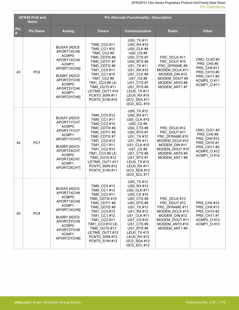
QFN48 Pin# andName
Pin Alternate Functionality / Description
Pin# Pin Name Analog Timers Communication Radio Other
43 PC6
BUSAX [ADC0:APORT1XCH6
ACMP0:APORT1XCH6
ACMP1:APORT1XCH6]
BUSBY [ADC0:APORT2YCH6
ACMP0:APORT2YCH6
ACMP1:APORT2YCH6]
TIM0_CC0 #11TIM0_CC1 #10TIM0_CC2 #9
TIM0_CDTI0 #8TIM0_CDTI1 #7TIM0_CDTI2 #6TIM1_CC0 #11TIM1_CC1 #10TIM1_CC2 #9
TIM1_CC3 #8 LE-TIM0_OUT0 #11
LETIM0_OUT1 #10PCNT0_S0IN #11PCNT0_S1IN #10
US0_TX #11US0_RX #10US0_CLK #9US0_CS #8
US0_CTS #7US0_RTS #6US1_TX #11US1_RX #10US1_CLK #9US1_CS #8
US1_CTS #7US1_RTS #6LEU0_TX #11LEU0_RX #10I2C0_SDA #11I2C0_SCL #10
FRC_DCLK #11FRC_DOUT #10
FRC_DFRAME #9MODEM_DCLK #11MODEM_DIN #10
MODEM_DOUT #9MODEM_ANT0 #8MODEM_ANT1 #7
CMU_CLK0 #2PRS_CH0 #8
PRS_CH9 #11PRS_CH10 #0PRS_CH11 #5ACMP0_O #11ACMP1_O #11
44 PC7
BUSAY [ADC0:APORT1YCH7
ACMP0:APORT1YCH7
ACMP1:APORT1YCH7]
BUSBX [ADC0:APORT2XCH7
ACMP0:APORT2XCH7
ACMP1:APORT2XCH7]
TIM0_CC0 #12TIM0_CC1 #11TIM0_CC2 #10TIM0_CDTI0 #9TIM0_CDTI1 #8TIM0_CDTI2 #7TIM1_CC0 #12TIM1_CC1 #11TIM1_CC2 #10
TIM1_CC3 #9 LE-TIM0_OUT0 #12
LETIM0_OUT1 #11PCNT0_S0IN #12PCNT0_S1IN #11
US0_TX #12US0_RX #11
US0_CLK #10US0_CS #9
US0_CTS #8US0_RTS #7US1_TX #12US1_RX #11
US1_CLK #10US1_CS #9
US1_CTS #8US1_RTS #7LEU0_TX #12LEU0_RX #11I2C0_SDA #12I2C0_SCL #11
FRC_DCLK #12FRC_DOUT #11
FRC_DFRAME #10MODEM_DCLK #12MODEM_DIN #11
MODEM_DOUT #10MODEM_ANT0 #9MODEM_ANT1 #8
CMU_CLK1 #2PRS_CH0 #9
PRS_CH9 #12PRS_CH10 #1PRS_CH11 #0ACMP0_O #12ACMP1_O #12
45 PC8
BUSAX [ADC0:APORT1XCH8
ACMP0:APORT1XCH8
ACMP1:APORT1XCH8]
BUSBY [ADC0:APORT2YCH8
ACMP0:APORT2YCH8
ACMP1:APORT2YCH8]
TIM0_CC0 #13TIM0_CC1 #12TIM0_CC2 #11
TIM0_CDTI0 #10TIM0_CDTI1 #9TIM0_CDTI2 #8TIM1_CC0 #13TIM1_CC1 #12TIM1_CC2 #11
TIM1_CC3 #10 LE-TIM0_OUT0 #13
LETIM0_OUT1 #12PCNT0_S0IN #13PCNT0_S1IN #12
US0_TX #13US0_RX #12
US0_CLK #11US0_CS #10US0_CTS #9US0_RTS #8US1_TX #13US1_RX #12
US1_CLK #11US1_CS #10US1_CTS #9US1_RTS #8LEU0_TX #13LEU0_RX #12I2C0_SDA #13I2C0_SCL #12
FRC_DCLK #13FRC_DOUT #12
FRC_DFRAME #11MODEM_DCLK #13MODEM_DIN #12
MODEM_DOUT #11MODEM_ANT0 #10MODEM_ANT1 #9
PRS_CH0 #10PRS_CH9 #13PRS_CH10 #2PRS_CH11 #1ACMP0_O #13ACMP1_O #13
EFR32FG1 Flex Gecko Proprietary Protocol SoCFamily Data SheetPin Definitions
silabs.com | Smart. Connected. Energy-friendly. Preliminary Rev. 0.97 | 119

QFN48 Pin# andName
Pin Alternate Functionality / Description
Pin# Pin Name Analog Timers Communication Radio Other
46 PC9
BUSAY [ADC0:APORT1YCH9
ACMP0:APORT1YCH9
ACMP1:APORT1YCH9]
BUSBX [ADC0:APORT2XCH9
ACMP0:APORT2XCH9
ACMP1:APORT2XCH9]
TIM0_CC0 #14TIM0_CC1 #13TIM0_CC2 #12
TIM0_CDTI0 #11TIM0_CDTI1 #10TIM0_CDTI2 #9TIM1_CC0 #14TIM1_CC1 #13TIM1_CC2 #12
TIM1_CC3 #11 LE-TIM0_OUT0 #14
LETIM0_OUT1 #13PCNT0_S0IN #14PCNT0_S1IN #13
US0_TX #14US0_RX #13
US0_CLK #12US0_CS #11
US0_CTS #10US0_RTS #9US1_TX #14US1_RX #13
US1_CLK #12US1_CS #11
US1_CTS #10US1_RTS #9LEU0_TX #14LEU0_RX #13I2C0_SDA #14I2C0_SCL #13
FRC_DCLK #14FRC_DOUT #13
FRC_DFRAME #12MODEM_DCLK #14MODEM_DIN #13
MODEM_DOUT #12MODEM_ANT0 #11MODEM_ANT1 #10
PRS_CH0 #11PRS_CH9 #14PRS_CH10 #3PRS_CH11 #2ACMP0_O #14ACMP1_O #14
47 PC10
BUSAX [ADC0:APORT1XCH10
ACMP0:APORT1XCH10
ACMP1:APORT1XCH10]
BUSBY [ADC0:APORT2YCH10
ACMP0:APORT2YCH10
ACMP1:APORT2YCH10]
TIM0_CC0 #15TIM0_CC1 #14TIM0_CC2 #13
TIM0_CDTI0 #12TIM0_CDTI1 #11TIM0_CDTI2 #10TIM1_CC0 #15TIM1_CC1 #14TIM1_CC2 #13
TIM1_CC3 #12 LE-TIM0_OUT0 #15
LETIM0_OUT1 #14PCNT0_S0IN #15PCNT0_S1IN #14
US0_TX #15US0_RX #14
US0_CLK #13US0_CS #12
US0_CTS #11US0_RTS #10US1_TX #15US1_RX #14
US1_CLK #13US1_CS #12
US1_CTS #11US1_RTS #10LEU0_TX #15LEU0_RX #14I2C0_SDA #15I2C0_SCL #14
FRC_DCLK #15FRC_DOUT #14
FRC_DFRAME #13MODEM_DCLK #15MODEM_DIN #14
MODEM_DOUT #13MODEM_ANT0 #12MODEM_ANT1 #11
CMU_CLK1 #3PRS_CH0 #12PRS_CH9 #15PRS_CH10 #4PRS_CH11 #3ACMP0_O #15ACMP1_O #15
GPIO_EM4WU12
48 PC11
BUSAY [ADC0:APORT1YCH11
ACMP0:APORT1YCH11
ACMP1:APORT1YCH11]
BUSBX [ADC0:APORT2XCH11
ACMP0:APORT2XCH11
ACMP1:APORT2XCH11]
TIM0_CC0 #16TIM0_CC1 #15TIM0_CC2 #14
TIM0_CDTI0 #13TIM0_CDTI1 #12TIM0_CDTI2 #11TIM1_CC0 #16TIM1_CC1 #15TIM1_CC2 #14
TIM1_CC3 #13 LE-TIM0_OUT0 #16
LETIM0_OUT1 #15PCNT0_S0IN #16PCNT0_S1IN #15
US0_TX #16US0_RX #15
US0_CLK #14US0_CS #13
US0_CTS #12US0_RTS #11US1_TX #16US1_RX #15
US1_CLK #14US1_CS #13
US1_CTS #12US1_RTS #11LEU0_TX #16LEU0_RX #15I2C0_SDA #16I2C0_SCL #15
FRC_DCLK #16FRC_DOUT #15
FRC_DFRAME #14MODEM_DCLK #16MODEM_DIN #15
MODEM_DOUT #14MODEM_ANT0 #13MODEM_ANT1 #12
CMU_CLK0 #3PRS_CH0 #13PRS_CH9 #16PRS_CH10 #5PRS_CH11 #4ACMP0_O #16ACMP1_O #16DBG_SWO #3
EFR32FG1 Flex Gecko Proprietary Protocol SoCFamily Data SheetPin Definitions
silabs.com | Smart. Connected. Energy-friendly. Preliminary Rev. 0.97 | 120
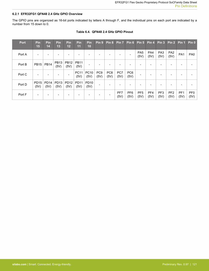
6.2.1 EFR32FG1 QFN48 2.4 GHz GPIO Overview
The GPIO pins are organized as 16-bit ports indicated by letters A through F, and the individual pins on each port are indicated by anumber from 15 down to 0.
Table 6.4. QFN48 2.4 GHz GPIO Pinout
Port Pin15
Pin14
Pin13
Pin12
Pin11
Pin10
Pin 9 Pin 8 Pin 7 Pin 6 Pin 5 Pin 4 Pin 3 Pin 2 Pin 1 Pin 0
Port A - - - - - - - - - - PA5(5V)
PA4(5V)
PA3(5V)
PA2(5V) PA1 PA0
Port B PB15 PB14 PB13(5V)
PB12(5V)
PB11(5V) - - - - - - - - - - -
Port C - - - - PC11(5V)
PC10(5V)
PC9(5V)
PC8(5V)
PC7(5V)
PC6(5V) - - - - - -
Port D PD15(5V)
PD14(5V)
PD13(5V)
PD12(5V)
PD11(5V)
PD10(5V) - - - - - - - - - -
Port F - - - - - - - - PF7(5V)
PF6(5V)
PF5(5V)
PF4(5V)
PF3(5V)
PF2(5V)
PF1(5V)
PF0(5V)
EFR32FG1 Flex Gecko Proprietary Protocol SoCFamily Data SheetPin Definitions
silabs.com | Smart. Connected. Energy-friendly. Preliminary Rev. 0.97 | 121
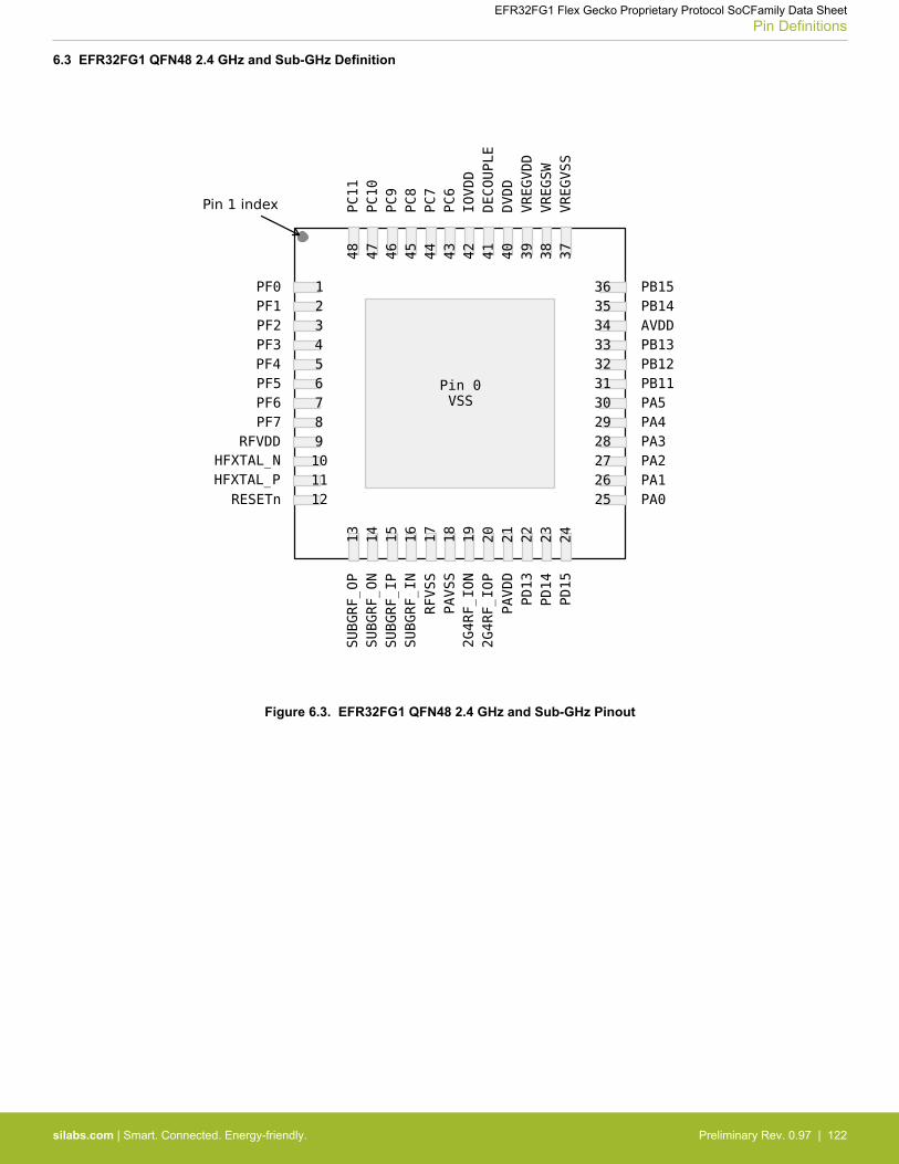
6.3 EFR32FG1 QFN48 2.4 GHz and Sub-GHz Definition
Figure 6.3. EFR32FG1 QFN48 2.4 GHz and Sub-GHz Pinout
EFR32FG1 Flex Gecko Proprietary Protocol SoCFamily Data SheetPin Definitions
silabs.com | Smart. Connected. Energy-friendly. Preliminary Rev. 0.97 | 122
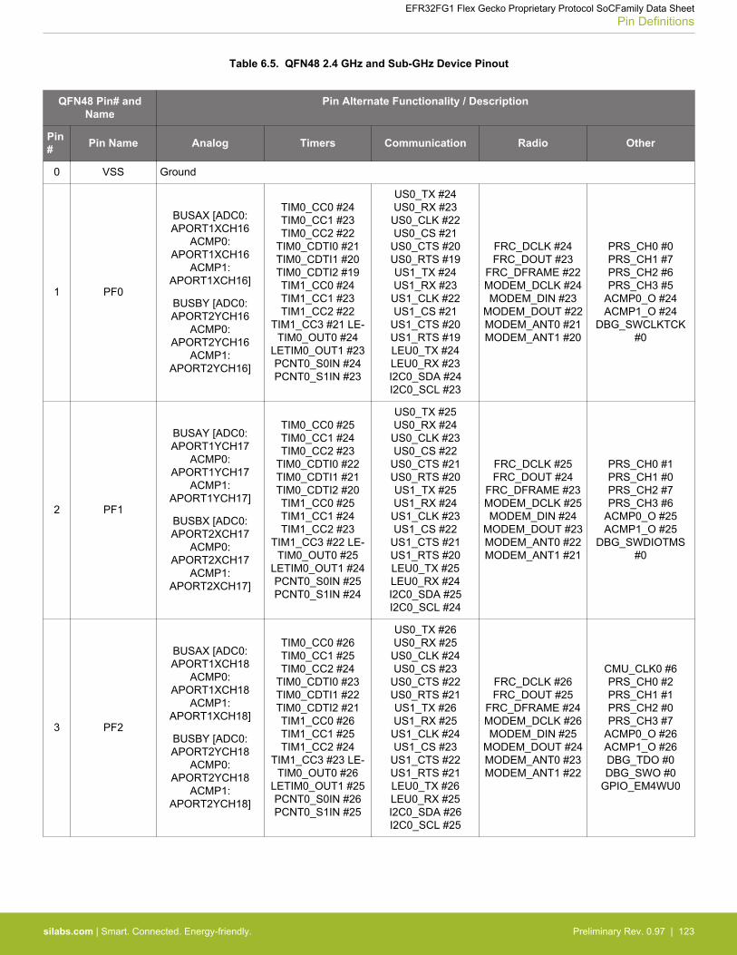
Table 6.5. QFN48 2.4 GHz and Sub-GHz Device Pinout
QFN48 Pin# andName
Pin Alternate Functionality / Description
Pin# Pin Name Analog Timers Communication Radio Other
0 VSS Ground
1 PF0
BUSAX [ADC0:APORT1XCH16
ACMP0:APORT1XCH16
ACMP1:APORT1XCH16]
BUSBY [ADC0:APORT2YCH16
ACMP0:APORT2YCH16
ACMP1:APORT2YCH16]
TIM0_CC0 #24TIM0_CC1 #23TIM0_CC2 #22
TIM0_CDTI0 #21TIM0_CDTI1 #20TIM0_CDTI2 #19TIM1_CC0 #24TIM1_CC1 #23TIM1_CC2 #22
TIM1_CC3 #21 LE-TIM0_OUT0 #24
LETIM0_OUT1 #23PCNT0_S0IN #24PCNT0_S1IN #23
US0_TX #24US0_RX #23
US0_CLK #22US0_CS #21
US0_CTS #20US0_RTS #19US1_TX #24US1_RX #23
US1_CLK #22US1_CS #21
US1_CTS #20US1_RTS #19LEU0_TX #24LEU0_RX #23I2C0_SDA #24I2C0_SCL #23
FRC_DCLK #24FRC_DOUT #23
FRC_DFRAME #22MODEM_DCLK #24MODEM_DIN #23
MODEM_DOUT #22MODEM_ANT0 #21MODEM_ANT1 #20
PRS_CH0 #0PRS_CH1 #7PRS_CH2 #6PRS_CH3 #5
ACMP0_O #24ACMP1_O #24
DBG_SWCLKTCK#0
2 PF1
BUSAY [ADC0:APORT1YCH17
ACMP0:APORT1YCH17
ACMP1:APORT1YCH17]
BUSBX [ADC0:APORT2XCH17
ACMP0:APORT2XCH17
ACMP1:APORT2XCH17]
TIM0_CC0 #25TIM0_CC1 #24TIM0_CC2 #23
TIM0_CDTI0 #22TIM0_CDTI1 #21TIM0_CDTI2 #20TIM1_CC0 #25TIM1_CC1 #24TIM1_CC2 #23
TIM1_CC3 #22 LE-TIM0_OUT0 #25
LETIM0_OUT1 #24PCNT0_S0IN #25PCNT0_S1IN #24
US0_TX #25US0_RX #24
US0_CLK #23US0_CS #22
US0_CTS #21US0_RTS #20US1_TX #25US1_RX #24
US1_CLK #23US1_CS #22
US1_CTS #21US1_RTS #20LEU0_TX #25LEU0_RX #24I2C0_SDA #25I2C0_SCL #24
FRC_DCLK #25FRC_DOUT #24
FRC_DFRAME #23MODEM_DCLK #25MODEM_DIN #24
MODEM_DOUT #23MODEM_ANT0 #22MODEM_ANT1 #21
PRS_CH0 #1PRS_CH1 #0PRS_CH2 #7PRS_CH3 #6
ACMP0_O #25ACMP1_O #25
DBG_SWDIOTMS#0
3 PF2
BUSAX [ADC0:APORT1XCH18
ACMP0:APORT1XCH18
ACMP1:APORT1XCH18]
BUSBY [ADC0:APORT2YCH18
ACMP0:APORT2YCH18
ACMP1:APORT2YCH18]
TIM0_CC0 #26TIM0_CC1 #25TIM0_CC2 #24
TIM0_CDTI0 #23TIM0_CDTI1 #22TIM0_CDTI2 #21TIM1_CC0 #26TIM1_CC1 #25TIM1_CC2 #24
TIM1_CC3 #23 LE-TIM0_OUT0 #26
LETIM0_OUT1 #25PCNT0_S0IN #26PCNT0_S1IN #25
US0_TX #26US0_RX #25
US0_CLK #24US0_CS #23
US0_CTS #22US0_RTS #21US1_TX #26US1_RX #25
US1_CLK #24US1_CS #23
US1_CTS #22US1_RTS #21LEU0_TX #26LEU0_RX #25I2C0_SDA #26I2C0_SCL #25
FRC_DCLK #26FRC_DOUT #25
FRC_DFRAME #24MODEM_DCLK #26MODEM_DIN #25
MODEM_DOUT #24MODEM_ANT0 #23MODEM_ANT1 #22
CMU_CLK0 #6PRS_CH0 #2PRS_CH1 #1PRS_CH2 #0PRS_CH3 #7
ACMP0_O #26ACMP1_O #26DBG_TDO #0DBG_SWO #0
GPIO_EM4WU0
EFR32FG1 Flex Gecko Proprietary Protocol SoCFamily Data SheetPin Definitions
silabs.com | Smart. Connected. Energy-friendly. Preliminary Rev. 0.97 | 123

QFN48 Pin# andName
Pin Alternate Functionality / Description
Pin# Pin Name Analog Timers Communication Radio Other
4 PF3
BUSAY [ADC0:APORT1YCH19
ACMP0:APORT1YCH19
ACMP1:APORT1YCH19]
BUSBX [ADC0:APORT2XCH19
ACMP0:APORT2XCH19
ACMP1:APORT2XCH19]
TIM0_CC0 #27TIM0_CC1 #26TIM0_CC2 #25
TIM0_CDTI0 #24TIM0_CDTI1 #23TIM0_CDTI2 #22TIM1_CC0 #27TIM1_CC1 #26TIM1_CC2 #25
TIM1_CC3 #24 LE-TIM0_OUT0 #27
LETIM0_OUT1 #26PCNT0_S0IN #27PCNT0_S1IN #26
US0_TX #27US0_RX #26
US0_CLK #25US0_CS #24
US0_CTS #23US0_RTS #22US1_TX #27US1_RX #26
US1_CLK #25US1_CS #24
US1_CTS #23US1_RTS #22LEU0_TX #27LEU0_RX #26I2C0_SDA #27I2C0_SCL #26
FRC_DCLK #27FRC_DOUT #26
FRC_DFRAME #25MODEM_DCLK #27MODEM_DIN #26
MODEM_DOUT #25MODEM_ANT0 #24MODEM_ANT1 #23
CMU_CLK1 #6PRS_CH0 #3PRS_CH1 #2PRS_CH2 #1PRS_CH3 #0
ACMP0_O #27ACMP1_O #27DBG_TDI #0
5 PF4
BUSAX [ADC0:APORT1XCH20
ACMP0:APORT1XCH20
ACMP1:APORT1XCH20]
BUSBY [ADC0:APORT2YCH20
ACMP0:APORT2YCH20
ACMP1:APORT2YCH20]
TIM0_CC0 #28TIM0_CC1 #27TIM0_CC2 #26
TIM0_CDTI0 #25TIM0_CDTI1 #24TIM0_CDTI2 #23TIM1_CC0 #28TIM1_CC1 #27TIM1_CC2 #26
TIM1_CC3 #25 LE-TIM0_OUT0 #28
LETIM0_OUT1 #27PCNT0_S0IN #28PCNT0_S1IN #27
US0_TX #28US0_RX #27
US0_CLK #26US0_CS #25
US0_CTS #24US0_RTS #23US1_TX #28US1_RX #27
US1_CLK #26US1_CS #25
US1_CTS #24US1_RTS #23LEU0_TX #28LEU0_RX #27I2C0_SDA #28I2C0_SCL #27
FRC_DCLK #28FRC_DOUT #27
FRC_DFRAME #26MODEM_DCLK #28MODEM_DIN #27
MODEM_DOUT #26MODEM_ANT0 #25MODEM_ANT1 #24
PRS_CH0 #4PRS_CH1 #3PRS_CH2 #2PRS_CH3 #1
ACMP0_O #28ACMP1_O #28
6 PF5
BUSAY [ADC0:APORT1YCH21
ACMP0:APORT1YCH21
ACMP1:APORT1YCH21]
BUSBX [ADC0:APORT2XCH21
ACMP0:APORT2XCH21
ACMP1:APORT2XCH21]
TIM0_CC0 #29TIM0_CC1 #28TIM0_CC2 #27
TIM0_CDTI0 #26TIM0_CDTI1 #25TIM0_CDTI2 #24TIM1_CC0 #29TIM1_CC1 #28TIM1_CC2 #27
TIM1_CC3 #26 LE-TIM0_OUT0 #29
LETIM0_OUT1 #28PCNT0_S0IN #29PCNT0_S1IN #28
US0_TX #29US0_RX #28
US0_CLK #27US0_CS #26
US0_CTS #25US0_RTS #24US1_TX #29US1_RX #28
US1_CLK #27US1_CS #26
US1_CTS #25US1_RTS #24LEU0_TX #29LEU0_RX #28I2C0_SDA #29I2C0_SCL #28
FRC_DCLK #29FRC_DOUT #28
FRC_DFRAME #27MODEM_DCLK #29MODEM_DIN #28
MODEM_DOUT #27MODEM_ANT0 #26MODEM_ANT1 #25
PRS_CH0 #5PRS_CH1 #4PRS_CH2 #3PRS_CH3 #2
ACMP0_O #29ACMP1_O #29
EFR32FG1 Flex Gecko Proprietary Protocol SoCFamily Data SheetPin Definitions
silabs.com | Smart. Connected. Energy-friendly. Preliminary Rev. 0.97 | 124
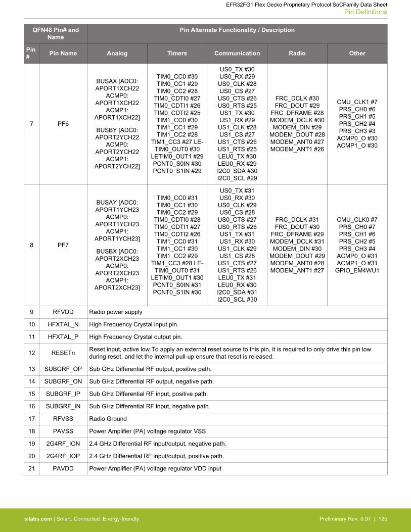
QFN48 Pin# andName
Pin Alternate Functionality / Description
Pin# Pin Name Analog Timers Communication Radio Other
7 PF6
BUSAX [ADC0:APORT1XCH22
ACMP0:APORT1XCH22
ACMP1:APORT1XCH22]
BUSBY [ADC0:APORT2YCH22
ACMP0:APORT2YCH22
ACMP1:APORT2YCH22]
TIM0_CC0 #30TIM0_CC1 #29TIM0_CC2 #28
TIM0_CDTI0 #27TIM0_CDTI1 #26TIM0_CDTI2 #25TIM1_CC0 #30TIM1_CC1 #29TIM1_CC2 #28
TIM1_CC3 #27 LE-TIM0_OUT0 #30
LETIM0_OUT1 #29PCNT0_S0IN #30PCNT0_S1IN #29
US0_TX #30US0_RX #29
US0_CLK #28US0_CS #27
US0_CTS #26US0_RTS #25US1_TX #30US1_RX #29
US1_CLK #28US1_CS #27
US1_CTS #26US1_RTS #25LEU0_TX #30LEU0_RX #29I2C0_SDA #30I2C0_SCL #29
FRC_DCLK #30FRC_DOUT #29
FRC_DFRAME #28MODEM_DCLK #30MODEM_DIN #29
MODEM_DOUT #28MODEM_ANT0 #27MODEM_ANT1 #26
CMU_CLK1 #7PRS_CH0 #6PRS_CH1 #5PRS_CH2 #4PRS_CH3 #3
ACMP0_O #30ACMP1_O #30
8 PF7
BUSAY [ADC0:APORT1YCH23
ACMP0:APORT1YCH23
ACMP1:APORT1YCH23]
BUSBX [ADC0:APORT2XCH23
ACMP0:APORT2XCH23
ACMP1:APORT2XCH23]
TIM0_CC0 #31TIM0_CC1 #30TIM0_CC2 #29
TIM0_CDTI0 #28TIM0_CDTI1 #27TIM0_CDTI2 #26TIM1_CC0 #31TIM1_CC1 #30TIM1_CC2 #29
TIM1_CC3 #28 LE-TIM0_OUT0 #31
LETIM0_OUT1 #30PCNT0_S0IN #31PCNT0_S1IN #30
US0_TX #31US0_RX #30
US0_CLK #29US0_CS #28
US0_CTS #27US0_RTS #26US1_TX #31US1_RX #30
US1_CLK #29US1_CS #28
US1_CTS #27US1_RTS #26LEU0_TX #31LEU0_RX #30I2C0_SDA #31I2C0_SCL #30
FRC_DCLK #31FRC_DOUT #30
FRC_DFRAME #29MODEM_DCLK #31MODEM_DIN #30
MODEM_DOUT #29MODEM_ANT0 #28MODEM_ANT1 #27
CMU_CLK0 #7PRS_CH0 #7PRS_CH1 #6PRS_CH2 #5PRS_CH3 #4
ACMP0_O #31ACMP1_O #31
GPIO_EM4WU1
9 RFVDD Radio power supply
10 HFXTAL_N High Frequency Crystal input pin.
11 HFXTAL_P High Frequency Crystal output pin.
12 RESETn Reset input, active low.To apply an external reset source to this pin, it is required to only drive this pin lowduring reset, and let the internal pull-up ensure that reset is released.
13 SUBGRF_OP Sub GHz Differential RF output, positive path.
14 SUBGRF_ON Sub GHz Differential RF output, negative path.
15 SUBGRF_IP Sub GHz Differential RF input, positive path.
16 SUBGRF_IN Sub GHz Differential RF input, negative path.
17 RFVSS Radio Ground
18 PAVSS Power Amplifier (PA) voltage regulator VSS
19 2G4RF_ION 2.4 GHz Differential RF input/output, negative path.
20 2G4RF_IOP 2.4 GHz Differential RF input/output, positive path.
21 PAVDD Power Amplifier (PA) voltage regulator VDD input
EFR32FG1 Flex Gecko Proprietary Protocol SoCFamily Data SheetPin Definitions
silabs.com | Smart. Connected. Energy-friendly. Preliminary Rev. 0.97 | 125

QFN48 Pin# andName
Pin Alternate Functionality / Description
Pin# Pin Name Analog Timers Communication Radio Other
22 PD13
BUSCY [ADC0:APORT3YCH5
ACMP0:APORT3YCH5
ACMP1:APORT3YCH5
IDAC0:APORT1YCH5]
BUSDX [ADC0:APORT4XCH5
ACMP0:APORT4XCH5
ACMP1:APORT4XCH5]
TIM0_CC0 #21TIM0_CC1 #20TIM0_CC2 #19
TIM0_CDTI0 #18TIM0_CDTI1 #17TIM0_CDTI2 #16TIM1_CC0 #21TIM1_CC1 #20TIM1_CC2 #19
TIM1_CC3 #18 LE-TIM0_OUT0 #21
LETIM0_OUT1 #20PCNT0_S0IN #21PCNT0_S1IN #20
US0_TX #21US0_RX #20
US0_CLK #19US0_CS #18
US0_CTS #17US0_RTS #16US1_TX #21US1_RX #20
US1_CLK #19US1_CS #18
US1_CTS #17US1_RTS #16LEU0_TX #21LEU0_RX #20I2C0_SDA #21I2C0_SCL #20
FRC_DCLK #21FRC_DOUT #20
FRC_DFRAME #19MODEM_DCLK #21MODEM_DIN #20
MODEM_DOUT #19MODEM_ANT0 #18MODEM_ANT1 #17
PRS_CH3 #12PRS_CH4 #4PRS_CH5 #3
PRS_CH6 #15ACMP0_O #21ACMP1_O #21
23 PD14
BUSCX [ADC0:APORT3XCH6
ACMP0:APORT3XCH6
ACMP1:APORT3XCH6
IDAC0:APORT1XCH6]
BUSDY [ADC0:APORT4YCH6
ACMP0:APORT4YCH6
ACMP1:APORT4YCH6]
TIM0_CC0 #22TIM0_CC1 #21TIM0_CC2 #20
TIM0_CDTI0 #19TIM0_CDTI1 #18TIM0_CDTI2 #17TIM1_CC0 #22TIM1_CC1 #21TIM1_CC2 #20
TIM1_CC3 #19 LE-TIM0_OUT0 #22
LETIM0_OUT1 #21PCNT0_S0IN #22PCNT0_S1IN #21
US0_TX #22US0_RX #21
US0_CLK #20US0_CS #19
US0_CTS #18US0_RTS #17US1_TX #22US1_RX #21
US1_CLK #20US1_CS #19
US1_CTS #18US1_RTS #17LEU0_TX #22LEU0_RX #21I2C0_SDA #22I2C0_SCL #21
FRC_DCLK #22FRC_DOUT #21
FRC_DFRAME #20MODEM_DCLK #22MODEM_DIN #21
MODEM_DOUT #20MODEM_ANT0 #19MODEM_ANT1 #18
CMU_CLK0 #5PRS_CH3 #13PRS_CH4 #5PRS_CH5 #4
PRS_CH6 #16ACMP0_O #22ACMP1_O #22
GPIO_EM4WU4
24 PD15
BUSCY [ADC0:APORT3YCH7
ACMP0:APORT3YCH7
ACMP1:APORT3YCH7
IDAC0:APORT1YCH7]
BUSDX [ADC0:APORT4XCH7
ACMP0:APORT4XCH7
ACMP1:APORT4XCH7]
TIM0_CC0 #23TIM0_CC1 #22TIM0_CC2 #21
TIM0_CDTI0 #20TIM0_CDTI1 #19TIM0_CDTI2 #18TIM1_CC0 #23TIM1_CC1 #22TIM1_CC2 #21
TIM1_CC3 #20 LE-TIM0_OUT0 #23
LETIM0_OUT1 #22PCNT0_S0IN #23PCNT0_S1IN #22
US0_TX #23US0_RX #22
US0_CLK #21US0_CS #20
US0_CTS #19US0_RTS #18US1_TX #23US1_RX #22
US1_CLK #21US1_CS #20
US1_CTS #19US1_RTS #18LEU0_TX #23LEU0_RX #22I2C0_SDA #23I2C0_SCL #22
FRC_DCLK #23FRC_DOUT #22
FRC_DFRAME #21MODEM_DCLK #23MODEM_DIN #22
MODEM_DOUT #21MODEM_ANT0 #20MODEM_ANT1 #19
CMU_CLK1 #5PRS_CH3 #14PRS_CH4 #6PRS_CH5 #5
PRS_CH6 #17ACMP0_O #23ACMP1_O #23DBG_SWO #2
EFR32FG1 Flex Gecko Proprietary Protocol SoCFamily Data SheetPin Definitions
silabs.com | Smart. Connected. Energy-friendly. Preliminary Rev. 0.97 | 126

QFN48 Pin# andName
Pin Alternate Functionality / Description
Pin# Pin Name Analog Timers Communication Radio Other
25 PA0
ADC0_EXTN
BUSCX [ADC0:APORT3XCH8
ACMP0:APORT3XCH8
ACMP1:APORT3XCH8
IDAC0:APORT1XCH8]
BUSDY [ADC0:APORT4YCH8
ACMP0:APORT4YCH8
ACMP1:APORT4YCH8]
TIM0_CC0 #0TIM0_CC1 #31TIM0_CC2 #30
TIM0_CDTI0 #29TIM0_CDTI1 #28TIM0_CDTI2 #27
TIM1_CC0 #0TIM1_CC1 #31TIM1_CC2 #30
TIM1_CC3 #29 LE-TIM0_OUT0 #0 LE-
TIM0_OUT1 #31PCNT0_S0IN #0PCNT0_S1IN #31
US0_TX #0US0_RX #31
US0_CLK #30US0_CS #29
US0_CTS #28US0_RTS #27
US1_TX #0US1_RX #31
US1_CLK #30US1_CS #29
US1_CTS #28US1_RTS #27LEU0_TX #0
LEU0_RX #31I2C0_SDA #0I2C0_SCL #31
FRC_DCLK #0FRC_DOUT #31
FRC_DFRAME #30MODEM_DCLK #0MODEM_DIN #31
MODEM_DOUT #30MODEM_ANT0 #29MODEM_ANT1 #28
CMU_CLK1 #0PRS_CH6 #0
PRS_CH7 #10PRS_CH8 #9PRS_CH9 #8ACMP0_O #0ACMP1_O #0
26 PA1
ADC0_EXTP
BUSCY [ADC0:APORT3YCH9
ACMP0:APORT3YCH9
ACMP1:APORT3YCH9
IDAC0:APORT1YCH9]
BUSDX [ADC0:APORT4XCH9
ACMP0:APORT4XCH9
ACMP1:APORT4XCH9]
TIM0_CC0 #1TIM0_CC1 #0TIM0_CC2 #31
TIM0_CDTI0 #30TIM0_CDTI1 #29TIM0_CDTI2 #28
TIM1_CC0 #1TIM1_CC1 #0TIM1_CC2 #31
TIM1_CC3 #30 LE-TIM0_OUT0 #1 LE-
TIM0_OUT1 #0PCNT0_S0IN #1PCNT0_S1IN #0
US0_TX #1US0_RX #0
US0_CLK #31US0_CS #30
US0_CTS #29US0_RTS #28
US1_TX #1US1_RX #0
US1_CLK #31US1_CS #30
US1_CTS #29US1_RTS #28LEU0_TX #1LEU0_RX #0I2C0_SDA #1I2C0_SCL #0
FRC_DCLK #1FRC_DOUT #0
FRC_DFRAME #31MODEM_DCLK #1MODEM_DIN #0
MODEM_DOUT #31MODEM_ANT0 #30MODEM_ANT1 #29
CMU_CLK0 #0PRS_CH6 #1PRS_CH7 #0
PRS_CH8 #10PRS_CH9 #9ACMP0_O #1ACMP1_O #1
27 PA2
BUSCX [ADC0:APORT3XCH10
ACMP0:APORT3XCH10
ACMP1:APORT3XCH10
IDAC0:APORT1XCH10]
BUSDY [ADC0:APORT4YCH10
ACMP0:APORT4YCH10
ACMP1:APORT4YCH10]
TIM0_CC0 #2TIM0_CC1 #1TIM0_CC2 #0
TIM0_CDTI0 #31TIM0_CDTI1 #30TIM0_CDTI2 #29
TIM1_CC0 #2TIM1_CC1 #1TIM1_CC2 #0
TIM1_CC3 #31 LE-TIM0_OUT0 #2 LE-
TIM0_OUT1 #1PCNT0_S0IN #2PCNT0_S1IN #1
US0_TX #2US0_RX #1
US0_CLK #0US0_CS #31
US0_CTS #30US0_RTS #29
US1_TX #2US1_RX #1
US1_CLK #0US1_CS #31
US1_CTS #30US1_RTS #29LEU0_TX #2LEU0_RX #1I2C0_SDA #2I2C0_SCL #1
FRC_DCLK #2FRC_DOUT #1
FRC_DFRAME #0MODEM_DCLK #2MODEM_DIN #1
MODEM_DOUT #0MODEM_ANT0 #31MODEM_ANT1 #30
PRS_CH6 #2PRS_CH7 #1PRS_CH8 #0
PRS_CH9 #10ACMP0_O #2ACMP1_O #2
EFR32FG1 Flex Gecko Proprietary Protocol SoCFamily Data SheetPin Definitions
silabs.com | Smart. Connected. Energy-friendly. Preliminary Rev. 0.97 | 127

QFN48 Pin# andName
Pin Alternate Functionality / Description
Pin# Pin Name Analog Timers Communication Radio Other
28 PA3
BUSCY [ADC0:APORT3YCH11
ACMP0:APORT3YCH11
ACMP1:APORT3YCH11
IDAC0:APORT1YCH11]
BUSDX [ADC0:APORT4XCH11
ACMP0:APORT4XCH11
ACMP1:APORT4XCH11]
TIM0_CC0 #3TIM0_CC1 #2TIM0_CC2 #1
TIM0_CDTI0 #0TIM0_CDTI1 #31TIM0_CDTI2 #30
TIM1_CC0 #3TIM1_CC1 #2TIM1_CC2 #1
TIM1_CC3 #0 LE-TIM0_OUT0 #3 LE-
TIM0_OUT1 #2PCNT0_S0IN #3PCNT0_S1IN #2
US0_TX #3US0_RX #2
US0_CLK #1US0_CS #0
US0_CTS #31US0_RTS #30
US1_TX #3US1_RX #2
US1_CLK #1US1_CS #0
US1_CTS #31US1_RTS #30LEU0_TX #3LEU0_RX #2I2C0_SDA #3I2C0_SCL #2
FRC_DCLK #3FRC_DOUT #2
FRC_DFRAME #1MODEM_DCLK #3MODEM_DIN #2
MODEM_DOUT #1MODEM_ANT0 #0
MODEM_ANT1 #31
PRS_CH6 #3PRS_CH7 #2PRS_CH8 #1PRS_CH9 #0ACMP0_O #3ACMP1_O #3
GPIO_EM4WU8
29 PA4
BUSCX [ADC0:APORT3XCH12
ACMP0:APORT3XCH12
ACMP1:APORT3XCH12
IDAC0:APORT1XCH12]
BUSDY [ADC0:APORT4YCH12
ACMP0:APORT4YCH12
ACMP1:APORT4YCH12]
TIM0_CC0 #4TIM0_CC1 #3TIM0_CC2 #2
TIM0_CDTI0 #1TIM0_CDTI1 #0TIM0_CDTI2 #31
TIM1_CC0 #4TIM1_CC1 #3TIM1_CC2 #2
TIM1_CC3 #1 LE-TIM0_OUT0 #4 LE-
TIM0_OUT1 #3PCNT0_S0IN #4PCNT0_S1IN #3
US0_TX #4US0_RX #3
US0_CLK #2US0_CS #1
US0_CTS #0US0_RTS #31
US1_TX #4US1_RX #3
US1_CLK #2US1_CS #1
US1_CTS #0US1_RTS #31LEU0_TX #4LEU0_RX #3I2C0_SDA #4I2C0_SCL #3
FRC_DCLK #4FRC_DOUT #3
FRC_DFRAME #2MODEM_DCLK #4MODEM_DIN #3
MODEM_DOUT #2MODEM_ANT0 #1MODEM_ANT1 #0
PRS_CH6 #4PRS_CH7 #3PRS_CH8 #2PRS_CH9 #1ACMP0_O #4ACMP1_O #4
30 PA5
BUSCY [ADC0:APORT3YCH13
ACMP0:APORT3YCH13
ACMP1:APORT3YCH13
IDAC0:APORT1YCH13]
BUSDX [ADC0:APORT4XCH13
ACMP0:APORT4XCH13
ACMP1:APORT4XCH13]
TIM0_CC0 #5TIM0_CC1 #4TIM0_CC2 #3
TIM0_CDTI0 #2TIM0_CDTI1 #1TIM0_CDTI2 #0TIM1_CC0 #5TIM1_CC1 #4TIM1_CC2 #3
TIM1_CC3 #2 LE-TIM0_OUT0 #5 LE-
TIM0_OUT1 #4PCNT0_S0IN #5PCNT0_S1IN #4
US0_TX #5US0_RX #4
US0_CLK #3US0_CS #2
US0_CTS #1US0_RTS #0US1_TX #5US1_RX #4
US1_CLK #3US1_CS #2
US1_CTS #1US1_RTS #0LEU0_TX #5LEU0_RX #4I2C0_SDA #5I2C0_SCL #4
FRC_DCLK #5FRC_DOUT #4
FRC_DFRAME #3MODEM_DCLK #5MODEM_DIN #4
MODEM_DOUT #3MODEM_ANT0 #2MODEM_ANT1 #1
PRS_CH6 #5PRS_CH7 #4PRS_CH8 #3PRS_CH9 #2ACMP0_O #5ACMP1_O #5
EFR32FG1 Flex Gecko Proprietary Protocol SoCFamily Data SheetPin Definitions
silabs.com | Smart. Connected. Energy-friendly. Preliminary Rev. 0.97 | 128

QFN48 Pin# andName
Pin Alternate Functionality / Description
Pin# Pin Name Analog Timers Communication Radio Other
31 PB11
BUSCY [ADC0:APORT3YCH27
ACMP0:APORT3YCH27
ACMP1:APORT3YCH27
IDAC0:APORT1YCH27]
BUSDX [ADC0:APORT4XCH27
ACMP0:APORT4XCH27
ACMP1:APORT4XCH27]
TIM0_CC0 #6TIM0_CC1 #5TIM0_CC2 #4
TIM0_CDTI0 #3TIM0_CDTI1 #2TIM0_CDTI2 #1TIM1_CC0 #6TIM1_CC1 #5TIM1_CC2 #4
TIM1_CC3 #3 LE-TIM0_OUT0 #6 LE-
TIM0_OUT1 #5PCNT0_S0IN #6PCNT0_S1IN #5
US0_TX #6US0_RX #5
US0_CLK #4US0_CS #3
US0_CTS #2US0_RTS #1US1_TX #6US1_RX #5
US1_CLK #4US1_CS #3
US1_CTS #2US1_RTS #1LEU0_TX #6LEU0_RX #5I2C0_SDA #6I2C0_SCL #5
FRC_DCLK #6FRC_DOUT #5
FRC_DFRAME #4MODEM_DCLK #6MODEM_DIN #5
MODEM_DOUT #4MODEM_ANT0 #3MODEM_ANT1 #2
PRS_CH6 #6PRS_CH7 #5PRS_CH8 #4PRS_CH9 #3ACMP0_O #6ACMP1_O #6
32 PB12
BUSCX [ADC0:APORT3XCH28
ACMP0:APORT3XCH28
ACMP1:APORT3XCH28
IDAC0:APORT1XCH28]
BUSDY [ADC0:APORT4YCH28
ACMP0:APORT4YCH28
ACMP1:APORT4YCH28]
TIM0_CC0 #7TIM0_CC1 #6TIM0_CC2 #5
TIM0_CDTI0 #4TIM0_CDTI1 #3TIM0_CDTI2 #2TIM1_CC0 #7TIM1_CC1 #6TIM1_CC2 #5
TIM1_CC3 #4 LE-TIM0_OUT0 #7 LE-
TIM0_OUT1 #6PCNT0_S0IN #7PCNT0_S1IN #6
US0_TX #7US0_RX #6
US0_CLK #5US0_CS #4
US0_CTS #3US0_RTS #2US1_TX #7US1_RX #6
US1_CLK #5US1_CS #4
US1_CTS #3US1_RTS #2LEU0_TX #7LEU0_RX #6I2C0_SDA #7I2C0_SCL #6
FRC_DCLK #7FRC_DOUT #6
FRC_DFRAME #5MODEM_DCLK #7MODEM_DIN #6
MODEM_DOUT #5MODEM_ANT0 #4MODEM_ANT1 #3
PRS_CH6 #7PRS_CH7 #6PRS_CH8 #5PRS_CH9 #4ACMP0_O #7ACMP1_O #7
33 PB13
BUSCY [ADC0:APORT3YCH29
ACMP0:APORT3YCH29
ACMP1:APORT3YCH29
IDAC0:APORT1YCH29]
BUSDX [ADC0:APORT4XCH29
ACMP0:APORT4XCH29
ACMP1:APORT4XCH29]
TIM0_CC0 #8TIM0_CC1 #7TIM0_CC2 #6
TIM0_CDTI0 #5TIM0_CDTI1 #4TIM0_CDTI2 #3TIM1_CC0 #8TIM1_CC1 #7TIM1_CC2 #6
TIM1_CC3 #5 LE-TIM0_OUT0 #8 LE-
TIM0_OUT1 #7PCNT0_S0IN #8PCNT0_S1IN #7
US0_TX #8US0_RX #7
US0_CLK #6US0_CS #5
US0_CTS #4US0_RTS #3US1_TX #8US1_RX #7
US1_CLK #6US1_CS #5
US1_CTS #4US1_RTS #3LEU0_TX #8LEU0_RX #7I2C0_SDA #8I2C0_SCL #7
FRC_DCLK #8FRC_DOUT #7
FRC_DFRAME #6MODEM_DCLK #8MODEM_DIN #7
MODEM_DOUT #6MODEM_ANT0 #5MODEM_ANT1 #4
PRS_CH6 #8PRS_CH7 #7PRS_CH8 #6PRS_CH9 #5ACMP0_O #8ACMP1_O #8DBG_SWO #1
GPIO_EM4WU9
34 AVDD Analog power supply.
EFR32FG1 Flex Gecko Proprietary Protocol SoCFamily Data SheetPin Definitions
silabs.com | Smart. Connected. Energy-friendly. Preliminary Rev. 0.97 | 129
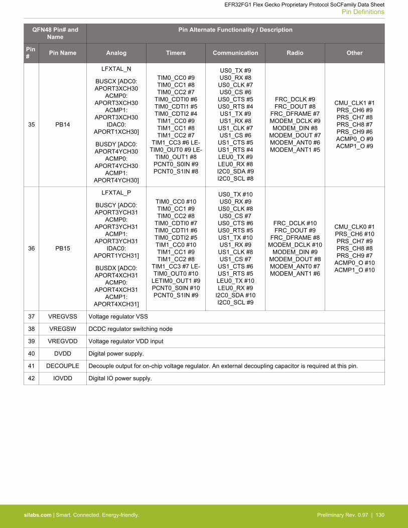
QFN48 Pin# andName
Pin Alternate Functionality / Description
Pin# Pin Name Analog Timers Communication Radio Other
35 PB14
LFXTAL_N
BUSCX [ADC0:APORT3XCH30
ACMP0:APORT3XCH30
ACMP1:APORT3XCH30
IDAC0:APORT1XCH30]
BUSDY [ADC0:APORT4YCH30
ACMP0:APORT4YCH30
ACMP1:APORT4YCH30]
TIM0_CC0 #9TIM0_CC1 #8TIM0_CC2 #7
TIM0_CDTI0 #6TIM0_CDTI1 #5TIM0_CDTI2 #4TIM1_CC0 #9TIM1_CC1 #8TIM1_CC2 #7
TIM1_CC3 #6 LE-TIM0_OUT0 #9 LE-
TIM0_OUT1 #8PCNT0_S0IN #9PCNT0_S1IN #8
US0_TX #9US0_RX #8
US0_CLK #7US0_CS #6
US0_CTS #5US0_RTS #4US1_TX #9US1_RX #8
US1_CLK #7US1_CS #6
US1_CTS #5US1_RTS #4LEU0_TX #9LEU0_RX #8I2C0_SDA #9I2C0_SCL #8
FRC_DCLK #9FRC_DOUT #8
FRC_DFRAME #7MODEM_DCLK #9MODEM_DIN #8
MODEM_DOUT #7MODEM_ANT0 #6MODEM_ANT1 #5
CMU_CLK1 #1PRS_CH6 #9PRS_CH7 #8PRS_CH8 #7PRS_CH9 #6ACMP0_O #9ACMP1_O #9
36 PB15
LFXTAL_P
BUSCY [ADC0:APORT3YCH31
ACMP0:APORT3YCH31
ACMP1:APORT3YCH31
IDAC0:APORT1YCH31]
BUSDX [ADC0:APORT4XCH31
ACMP0:APORT4XCH31
ACMP1:APORT4XCH31]
TIM0_CC0 #10TIM0_CC1 #9TIM0_CC2 #8
TIM0_CDTI0 #7TIM0_CDTI1 #6TIM0_CDTI2 #5TIM1_CC0 #10TIM1_CC1 #9TIM1_CC2 #8
TIM1_CC3 #7 LE-TIM0_OUT0 #10
LETIM0_OUT1 #9PCNT0_S0IN #10PCNT0_S1IN #9
US0_TX #10US0_RX #9
US0_CLK #8US0_CS #7
US0_CTS #6US0_RTS #5US1_TX #10US1_RX #9
US1_CLK #8US1_CS #7
US1_CTS #6US1_RTS #5LEU0_TX #10LEU0_RX #9
I2C0_SDA #10I2C0_SCL #9
FRC_DCLK #10FRC_DOUT #9
FRC_DFRAME #8MODEM_DCLK #10
MODEM_DIN #9MODEM_DOUT #8MODEM_ANT0 #7MODEM_ANT1 #6
CMU_CLK0 #1PRS_CH6 #10PRS_CH7 #9PRS_CH8 #8PRS_CH9 #7
ACMP0_O #10ACMP1_O #10
37 VREGVSS Voltage regulator VSS
38 VREGSW DCDC regulator switching node
39 VREGVDD Voltage regulator VDD input
40 DVDD Digital power supply.
41 DECOUPLE Decouple output for on-chip voltage regulator. An external decoupling capacitor is required at this pin.
42 IOVDD Digital IO power supply.
EFR32FG1 Flex Gecko Proprietary Protocol SoCFamily Data SheetPin Definitions
silabs.com | Smart. Connected. Energy-friendly. Preliminary Rev. 0.97 | 130

QFN48 Pin# andName
Pin Alternate Functionality / Description
Pin# Pin Name Analog Timers Communication Radio Other
43 PC6
BUSAX [ADC0:APORT1XCH6
ACMP0:APORT1XCH6
ACMP1:APORT1XCH6]
BUSBY [ADC0:APORT2YCH6
ACMP0:APORT2YCH6
ACMP1:APORT2YCH6]
TIM0_CC0 #11TIM0_CC1 #10TIM0_CC2 #9
TIM0_CDTI0 #8TIM0_CDTI1 #7TIM0_CDTI2 #6TIM1_CC0 #11TIM1_CC1 #10TIM1_CC2 #9
TIM1_CC3 #8 LE-TIM0_OUT0 #11
LETIM0_OUT1 #10PCNT0_S0IN #11PCNT0_S1IN #10
US0_TX #11US0_RX #10US0_CLK #9US0_CS #8
US0_CTS #7US0_RTS #6US1_TX #11US1_RX #10US1_CLK #9US1_CS #8
US1_CTS #7US1_RTS #6LEU0_TX #11LEU0_RX #10I2C0_SDA #11I2C0_SCL #10
FRC_DCLK #11FRC_DOUT #10
FRC_DFRAME #9MODEM_DCLK #11MODEM_DIN #10
MODEM_DOUT #9MODEM_ANT0 #8MODEM_ANT1 #7
CMU_CLK0 #2PRS_CH0 #8
PRS_CH9 #11PRS_CH10 #0PRS_CH11 #5ACMP0_O #11ACMP1_O #11
44 PC7
BUSAY [ADC0:APORT1YCH7
ACMP0:APORT1YCH7
ACMP1:APORT1YCH7]
BUSBX [ADC0:APORT2XCH7
ACMP0:APORT2XCH7
ACMP1:APORT2XCH7]
TIM0_CC0 #12TIM0_CC1 #11TIM0_CC2 #10TIM0_CDTI0 #9TIM0_CDTI1 #8TIM0_CDTI2 #7TIM1_CC0 #12TIM1_CC1 #11TIM1_CC2 #10
TIM1_CC3 #9 LE-TIM0_OUT0 #12
LETIM0_OUT1 #11PCNT0_S0IN #12PCNT0_S1IN #11
US0_TX #12US0_RX #11
US0_CLK #10US0_CS #9
US0_CTS #8US0_RTS #7US1_TX #12US1_RX #11
US1_CLK #10US1_CS #9
US1_CTS #8US1_RTS #7LEU0_TX #12LEU0_RX #11I2C0_SDA #12I2C0_SCL #11
FRC_DCLK #12FRC_DOUT #11
FRC_DFRAME #10MODEM_DCLK #12MODEM_DIN #11
MODEM_DOUT #10MODEM_ANT0 #9MODEM_ANT1 #8
CMU_CLK1 #2PRS_CH0 #9
PRS_CH9 #12PRS_CH10 #1PRS_CH11 #0ACMP0_O #12ACMP1_O #12
45 PC8
BUSAX [ADC0:APORT1XCH8
ACMP0:APORT1XCH8
ACMP1:APORT1XCH8]
BUSBY [ADC0:APORT2YCH8
ACMP0:APORT2YCH8
ACMP1:APORT2YCH8]
TIM0_CC0 #13TIM0_CC1 #12TIM0_CC2 #11
TIM0_CDTI0 #10TIM0_CDTI1 #9TIM0_CDTI2 #8TIM1_CC0 #13TIM1_CC1 #12TIM1_CC2 #11
TIM1_CC3 #10 LE-TIM0_OUT0 #13
LETIM0_OUT1 #12PCNT0_S0IN #13PCNT0_S1IN #12
US0_TX #13US0_RX #12
US0_CLK #11US0_CS #10US0_CTS #9US0_RTS #8US1_TX #13US1_RX #12
US1_CLK #11US1_CS #10US1_CTS #9US1_RTS #8LEU0_TX #13LEU0_RX #12I2C0_SDA #13I2C0_SCL #12
FRC_DCLK #13FRC_DOUT #12
FRC_DFRAME #11MODEM_DCLK #13MODEM_DIN #12
MODEM_DOUT #11MODEM_ANT0 #10MODEM_ANT1 #9
PRS_CH0 #10PRS_CH9 #13PRS_CH10 #2PRS_CH11 #1ACMP0_O #13ACMP1_O #13
EFR32FG1 Flex Gecko Proprietary Protocol SoCFamily Data SheetPin Definitions
silabs.com | Smart. Connected. Energy-friendly. Preliminary Rev. 0.97 | 131
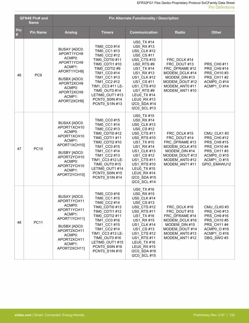
QFN48 Pin# andName
Pin Alternate Functionality / Description
Pin# Pin Name Analog Timers Communication Radio Other
46 PC9
BUSAY [ADC0:APORT1YCH9
ACMP0:APORT1YCH9
ACMP1:APORT1YCH9]
BUSBX [ADC0:APORT2XCH9
ACMP0:APORT2XCH9
ACMP1:APORT2XCH9]
TIM0_CC0 #14TIM0_CC1 #13TIM0_CC2 #12
TIM0_CDTI0 #11TIM0_CDTI1 #10TIM0_CDTI2 #9TIM1_CC0 #14TIM1_CC1 #13TIM1_CC2 #12
TIM1_CC3 #11 LE-TIM0_OUT0 #14
LETIM0_OUT1 #13PCNT0_S0IN #14PCNT0_S1IN #13
US0_TX #14US0_RX #13
US0_CLK #12US0_CS #11
US0_CTS #10US0_RTS #9US1_TX #14US1_RX #13
US1_CLK #12US1_CS #11
US1_CTS #10US1_RTS #9LEU0_TX #14LEU0_RX #13I2C0_SDA #14I2C0_SCL #13
FRC_DCLK #14FRC_DOUT #13
FRC_DFRAME #12MODEM_DCLK #14MODEM_DIN #13
MODEM_DOUT #12MODEM_ANT0 #11MODEM_ANT1 #10
PRS_CH0 #11PRS_CH9 #14PRS_CH10 #3PRS_CH11 #2ACMP0_O #14ACMP1_O #14
47 PC10
BUSAX [ADC0:APORT1XCH10
ACMP0:APORT1XCH10
ACMP1:APORT1XCH10]
BUSBY [ADC0:APORT2YCH10
ACMP0:APORT2YCH10
ACMP1:APORT2YCH10]
TIM0_CC0 #15TIM0_CC1 #14TIM0_CC2 #13
TIM0_CDTI0 #12TIM0_CDTI1 #11TIM0_CDTI2 #10TIM1_CC0 #15TIM1_CC1 #14TIM1_CC2 #13
TIM1_CC3 #12 LE-TIM0_OUT0 #15
LETIM0_OUT1 #14PCNT0_S0IN #15PCNT0_S1IN #14
US0_TX #15US0_RX #14
US0_CLK #13US0_CS #12
US0_CTS #11US0_RTS #10US1_TX #15US1_RX #14
US1_CLK #13US1_CS #12
US1_CTS #11US1_RTS #10LEU0_TX #15LEU0_RX #14I2C0_SDA #15I2C0_SCL #14
FRC_DCLK #15FRC_DOUT #14
FRC_DFRAME #13MODEM_DCLK #15MODEM_DIN #14
MODEM_DOUT #13MODEM_ANT0 #12MODEM_ANT1 #11
CMU_CLK1 #3PRS_CH0 #12PRS_CH9 #15PRS_CH10 #4PRS_CH11 #3ACMP0_O #15ACMP1_O #15
GPIO_EM4WU12
48 PC11
BUSAY [ADC0:APORT1YCH11
ACMP0:APORT1YCH11
ACMP1:APORT1YCH11]
BUSBX [ADC0:APORT2XCH11
ACMP0:APORT2XCH11
ACMP1:APORT2XCH11]
TIM0_CC0 #16TIM0_CC1 #15TIM0_CC2 #14
TIM0_CDTI0 #13TIM0_CDTI1 #12TIM0_CDTI2 #11TIM1_CC0 #16TIM1_CC1 #15TIM1_CC2 #14
TIM1_CC3 #13 LE-TIM0_OUT0 #16
LETIM0_OUT1 #15PCNT0_S0IN #16PCNT0_S1IN #15
US0_TX #16US0_RX #15
US0_CLK #14US0_CS #13
US0_CTS #12US0_RTS #11US1_TX #16US1_RX #15
US1_CLK #14US1_CS #13
US1_CTS #12US1_RTS #11LEU0_TX #16LEU0_RX #15I2C0_SDA #16I2C0_SCL #15
FRC_DCLK #16FRC_DOUT #15
FRC_DFRAME #14MODEM_DCLK #16MODEM_DIN #15
MODEM_DOUT #14MODEM_ANT0 #13MODEM_ANT1 #12
CMU_CLK0 #3PRS_CH0 #13PRS_CH9 #16PRS_CH10 #5PRS_CH11 #4ACMP0_O #16ACMP1_O #16DBG_SWO #3
EFR32FG1 Flex Gecko Proprietary Protocol SoCFamily Data SheetPin Definitions
silabs.com | Smart. Connected. Energy-friendly. Preliminary Rev. 0.97 | 132
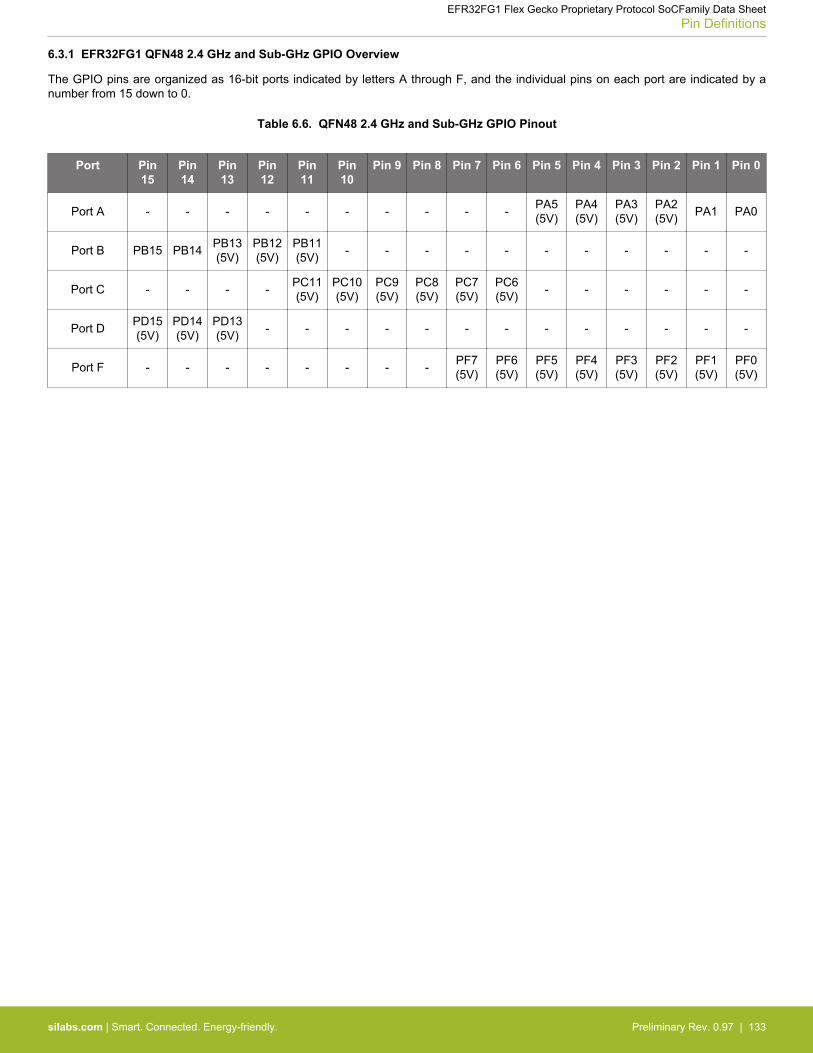
6.3.1 EFR32FG1 QFN48 2.4 GHz and Sub-GHz GPIO Overview
The GPIO pins are organized as 16-bit ports indicated by letters A through F, and the individual pins on each port are indicated by anumber from 15 down to 0.
Table 6.6. QFN48 2.4 GHz and Sub-GHz GPIO Pinout
Port Pin15
Pin14
Pin13
Pin12
Pin11
Pin10
Pin 9 Pin 8 Pin 7 Pin 6 Pin 5 Pin 4 Pin 3 Pin 2 Pin 1 Pin 0
Port A - - - - - - - - - - PA5(5V)
PA4(5V)
PA3(5V)
PA2(5V) PA1 PA0
Port B PB15 PB14 PB13(5V)
PB12(5V)
PB11(5V) - - - - - - - - - - -
Port C - - - - PC11(5V)
PC10(5V)
PC9(5V)
PC8(5V)
PC7(5V)
PC6(5V) - - - - - -
Port D PD15(5V)
PD14(5V)
PD13(5V) - - - - - - - - - - - - -
Port F - - - - - - - - PF7(5V)
PF6(5V)
PF5(5V)
PF4(5V)
PF3(5V)
PF2(5V)
PF1(5V)
PF0(5V)
EFR32FG1 Flex Gecko Proprietary Protocol SoCFamily Data SheetPin Definitions
silabs.com | Smart. Connected. Energy-friendly. Preliminary Rev. 0.97 | 133
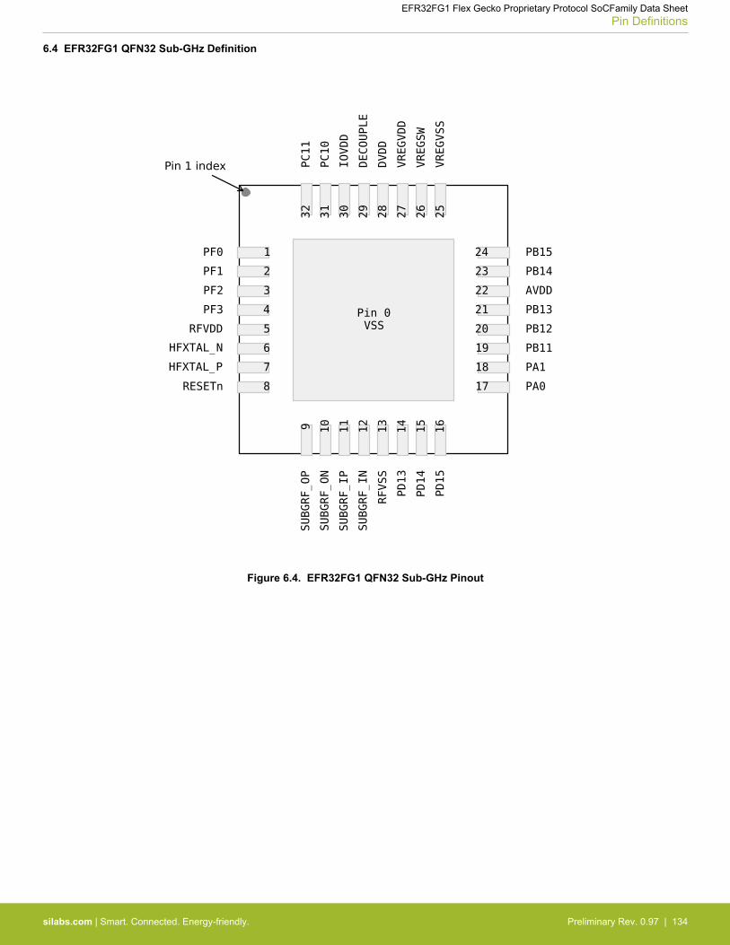
6.4 EFR32FG1 QFN32 Sub-GHz Definition
Figure 6.4. EFR32FG1 QFN32 Sub-GHz Pinout
EFR32FG1 Flex Gecko Proprietary Protocol SoCFamily Data SheetPin Definitions
silabs.com | Smart. Connected. Energy-friendly. Preliminary Rev. 0.97 | 134

Table 6.7. QFN32 Sub-GHz Device Pinout
QFN32 Pin# andName
Pin Alternate Functionality / Description
Pin# Pin Name Analog Timers Communication Radio Other
0 VSS Ground
1 PF0
BUSAX [ADC0:APORT1XCH16
ACMP0:APORT1XCH16
ACMP1:APORT1XCH16]
BUSBY [ADC0:APORT2YCH16
ACMP0:APORT2YCH16
ACMP1:APORT2YCH16]
TIM0_CC0 #24TIM0_CC1 #23TIM0_CC2 #22
TIM0_CDTI0 #21TIM0_CDTI1 #20TIM0_CDTI2 #19TIM1_CC0 #24TIM1_CC1 #23TIM1_CC2 #22
TIM1_CC3 #21 LE-TIM0_OUT0 #24
LETIM0_OUT1 #23PCNT0_S0IN #24PCNT0_S1IN #23
US0_TX #24US0_RX #23
US0_CLK #22US0_CS #21
US0_CTS #20US0_RTS #19US1_TX #24US1_RX #23
US1_CLK #22US1_CS #21
US1_CTS #20US1_RTS #19LEU0_TX #24LEU0_RX #23I2C0_SDA #24I2C0_SCL #23
FRC_DCLK #24FRC_DOUT #23
FRC_DFRAME #22MODEM_DCLK #24MODEM_DIN #23
MODEM_DOUT #22MODEM_ANT0 #21MODEM_ANT1 #20
PRS_CH0 #0PRS_CH1 #7PRS_CH2 #6PRS_CH3 #5
ACMP0_O #24ACMP1_O #24
DBG_SWCLKTCK#0
2 PF1
BUSAY [ADC0:APORT1YCH17
ACMP0:APORT1YCH17
ACMP1:APORT1YCH17]
BUSBX [ADC0:APORT2XCH17
ACMP0:APORT2XCH17
ACMP1:APORT2XCH17]
TIM0_CC0 #25TIM0_CC1 #24TIM0_CC2 #23
TIM0_CDTI0 #22TIM0_CDTI1 #21TIM0_CDTI2 #20TIM1_CC0 #25TIM1_CC1 #24TIM1_CC2 #23
TIM1_CC3 #22 LE-TIM0_OUT0 #25
LETIM0_OUT1 #24PCNT0_S0IN #25PCNT0_S1IN #24
US0_TX #25US0_RX #24
US0_CLK #23US0_CS #22
US0_CTS #21US0_RTS #20US1_TX #25US1_RX #24
US1_CLK #23US1_CS #22
US1_CTS #21US1_RTS #20LEU0_TX #25LEU0_RX #24I2C0_SDA #25I2C0_SCL #24
FRC_DCLK #25FRC_DOUT #24
FRC_DFRAME #23MODEM_DCLK #25MODEM_DIN #24
MODEM_DOUT #23MODEM_ANT0 #22MODEM_ANT1 #21
PRS_CH0 #1PRS_CH1 #0PRS_CH2 #7PRS_CH3 #6
ACMP0_O #25ACMP1_O #25
DBG_SWDIOTMS#0
3 PF2
BUSAX [ADC0:APORT1XCH18
ACMP0:APORT1XCH18
ACMP1:APORT1XCH18]
BUSBY [ADC0:APORT2YCH18
ACMP0:APORT2YCH18
ACMP1:APORT2YCH18]
TIM0_CC0 #26TIM0_CC1 #25TIM0_CC2 #24
TIM0_CDTI0 #23TIM0_CDTI1 #22TIM0_CDTI2 #21TIM1_CC0 #26TIM1_CC1 #25TIM1_CC2 #24
TIM1_CC3 #23 LE-TIM0_OUT0 #26
LETIM0_OUT1 #25PCNT0_S0IN #26PCNT0_S1IN #25
US0_TX #26US0_RX #25
US0_CLK #24US0_CS #23
US0_CTS #22US0_RTS #21US1_TX #26US1_RX #25
US1_CLK #24US1_CS #23
US1_CTS #22US1_RTS #21LEU0_TX #26LEU0_RX #25I2C0_SDA #26I2C0_SCL #25
FRC_DCLK #26FRC_DOUT #25
FRC_DFRAME #24MODEM_DCLK #26MODEM_DIN #25
MODEM_DOUT #24MODEM_ANT0 #23MODEM_ANT1 #22
CMU_CLK0 #6PRS_CH0 #2PRS_CH1 #1PRS_CH2 #0PRS_CH3 #7
ACMP0_O #26ACMP1_O #26DBG_TDO #0DBG_SWO #0
GPIO_EM4WU0
EFR32FG1 Flex Gecko Proprietary Protocol SoCFamily Data SheetPin Definitions
silabs.com | Smart. Connected. Energy-friendly. Preliminary Rev. 0.97 | 135
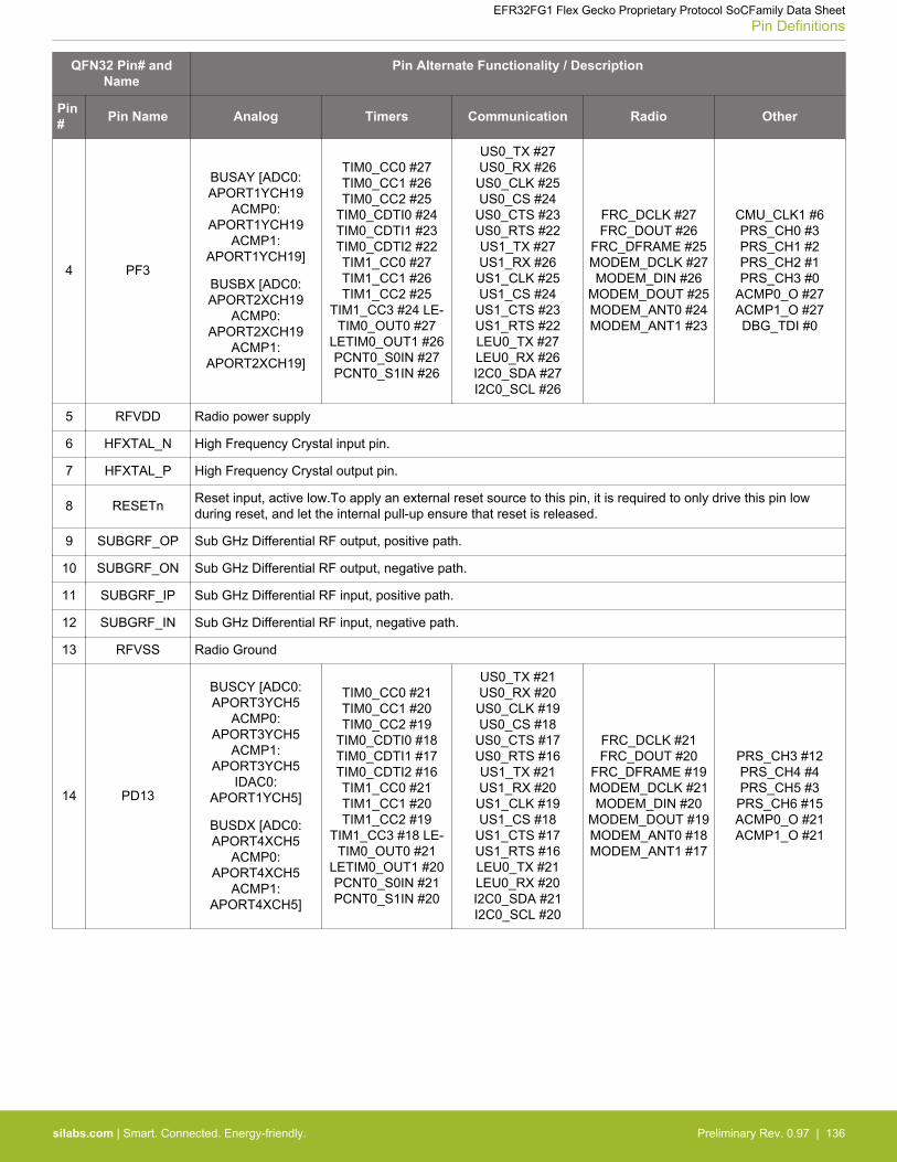
QFN32 Pin# andName
Pin Alternate Functionality / Description
Pin# Pin Name Analog Timers Communication Radio Other
4 PF3
BUSAY [ADC0:APORT1YCH19
ACMP0:APORT1YCH19
ACMP1:APORT1YCH19]
BUSBX [ADC0:APORT2XCH19
ACMP0:APORT2XCH19
ACMP1:APORT2XCH19]
TIM0_CC0 #27TIM0_CC1 #26TIM0_CC2 #25
TIM0_CDTI0 #24TIM0_CDTI1 #23TIM0_CDTI2 #22TIM1_CC0 #27TIM1_CC1 #26TIM1_CC2 #25
TIM1_CC3 #24 LE-TIM0_OUT0 #27
LETIM0_OUT1 #26PCNT0_S0IN #27PCNT0_S1IN #26
US0_TX #27US0_RX #26
US0_CLK #25US0_CS #24
US0_CTS #23US0_RTS #22US1_TX #27US1_RX #26
US1_CLK #25US1_CS #24
US1_CTS #23US1_RTS #22LEU0_TX #27LEU0_RX #26I2C0_SDA #27I2C0_SCL #26
FRC_DCLK #27FRC_DOUT #26
FRC_DFRAME #25MODEM_DCLK #27MODEM_DIN #26
MODEM_DOUT #25MODEM_ANT0 #24MODEM_ANT1 #23
CMU_CLK1 #6PRS_CH0 #3PRS_CH1 #2PRS_CH2 #1PRS_CH3 #0
ACMP0_O #27ACMP1_O #27DBG_TDI #0
5 RFVDD Radio power supply
6 HFXTAL_N High Frequency Crystal input pin.
7 HFXTAL_P High Frequency Crystal output pin.
8 RESETn Reset input, active low.To apply an external reset source to this pin, it is required to only drive this pin lowduring reset, and let the internal pull-up ensure that reset is released.
9 SUBGRF_OP Sub GHz Differential RF output, positive path.
10 SUBGRF_ON Sub GHz Differential RF output, negative path.
11 SUBGRF_IP Sub GHz Differential RF input, positive path.
12 SUBGRF_IN Sub GHz Differential RF input, negative path.
13 RFVSS Radio Ground
14 PD13
BUSCY [ADC0:APORT3YCH5
ACMP0:APORT3YCH5
ACMP1:APORT3YCH5
IDAC0:APORT1YCH5]
BUSDX [ADC0:APORT4XCH5
ACMP0:APORT4XCH5
ACMP1:APORT4XCH5]
TIM0_CC0 #21TIM0_CC1 #20TIM0_CC2 #19
TIM0_CDTI0 #18TIM0_CDTI1 #17TIM0_CDTI2 #16TIM1_CC0 #21TIM1_CC1 #20TIM1_CC2 #19
TIM1_CC3 #18 LE-TIM0_OUT0 #21
LETIM0_OUT1 #20PCNT0_S0IN #21PCNT0_S1IN #20
US0_TX #21US0_RX #20
US0_CLK #19US0_CS #18
US0_CTS #17US0_RTS #16US1_TX #21US1_RX #20
US1_CLK #19US1_CS #18
US1_CTS #17US1_RTS #16LEU0_TX #21LEU0_RX #20I2C0_SDA #21I2C0_SCL #20
FRC_DCLK #21FRC_DOUT #20
FRC_DFRAME #19MODEM_DCLK #21MODEM_DIN #20
MODEM_DOUT #19MODEM_ANT0 #18MODEM_ANT1 #17
PRS_CH3 #12PRS_CH4 #4PRS_CH5 #3
PRS_CH6 #15ACMP0_O #21ACMP1_O #21
EFR32FG1 Flex Gecko Proprietary Protocol SoCFamily Data SheetPin Definitions
silabs.com | Smart. Connected. Energy-friendly. Preliminary Rev. 0.97 | 136

QFN32 Pin# andName
Pin Alternate Functionality / Description
Pin# Pin Name Analog Timers Communication Radio Other
15 PD14
BUSCX [ADC0:APORT3XCH6
ACMP0:APORT3XCH6
ACMP1:APORT3XCH6
IDAC0:APORT1XCH6]
BUSDY [ADC0:APORT4YCH6
ACMP0:APORT4YCH6
ACMP1:APORT4YCH6]
TIM0_CC0 #22TIM0_CC1 #21TIM0_CC2 #20
TIM0_CDTI0 #19TIM0_CDTI1 #18TIM0_CDTI2 #17TIM1_CC0 #22TIM1_CC1 #21TIM1_CC2 #20
TIM1_CC3 #19 LE-TIM0_OUT0 #22
LETIM0_OUT1 #21PCNT0_S0IN #22PCNT0_S1IN #21
US0_TX #22US0_RX #21
US0_CLK #20US0_CS #19
US0_CTS #18US0_RTS #17US1_TX #22US1_RX #21
US1_CLK #20US1_CS #19
US1_CTS #18US1_RTS #17LEU0_TX #22LEU0_RX #21I2C0_SDA #22I2C0_SCL #21
FRC_DCLK #22FRC_DOUT #21
FRC_DFRAME #20MODEM_DCLK #22MODEM_DIN #21
MODEM_DOUT #20MODEM_ANT0 #19MODEM_ANT1 #18
CMU_CLK0 #5PRS_CH3 #13PRS_CH4 #5PRS_CH5 #4
PRS_CH6 #16ACMP0_O #22ACMP1_O #22
GPIO_EM4WU4
16 PD15
BUSCY [ADC0:APORT3YCH7
ACMP0:APORT3YCH7
ACMP1:APORT3YCH7
IDAC0:APORT1YCH7]
BUSDX [ADC0:APORT4XCH7
ACMP0:APORT4XCH7
ACMP1:APORT4XCH7]
TIM0_CC0 #23TIM0_CC1 #22TIM0_CC2 #21
TIM0_CDTI0 #20TIM0_CDTI1 #19TIM0_CDTI2 #18TIM1_CC0 #23TIM1_CC1 #22TIM1_CC2 #21
TIM1_CC3 #20 LE-TIM0_OUT0 #23
LETIM0_OUT1 #22PCNT0_S0IN #23PCNT0_S1IN #22
US0_TX #23US0_RX #22
US0_CLK #21US0_CS #20
US0_CTS #19US0_RTS #18US1_TX #23US1_RX #22
US1_CLK #21US1_CS #20
US1_CTS #19US1_RTS #18LEU0_TX #23LEU0_RX #22I2C0_SDA #23I2C0_SCL #22
FRC_DCLK #23FRC_DOUT #22
FRC_DFRAME #21MODEM_DCLK #23MODEM_DIN #22
MODEM_DOUT #21MODEM_ANT0 #20MODEM_ANT1 #19
CMU_CLK1 #5PRS_CH3 #14PRS_CH4 #6PRS_CH5 #5
PRS_CH6 #17ACMP0_O #23ACMP1_O #23DBG_SWO #2
17 PA0
ADC0_EXTN
BUSCX [ADC0:APORT3XCH8
ACMP0:APORT3XCH8
ACMP1:APORT3XCH8
IDAC0:APORT1XCH8]
BUSDY [ADC0:APORT4YCH8
ACMP0:APORT4YCH8
ACMP1:APORT4YCH8]
TIM0_CC0 #0TIM0_CC1 #31TIM0_CC2 #30
TIM0_CDTI0 #29TIM0_CDTI1 #28TIM0_CDTI2 #27
TIM1_CC0 #0TIM1_CC1 #31TIM1_CC2 #30
TIM1_CC3 #29 LE-TIM0_OUT0 #0 LE-
TIM0_OUT1 #31PCNT0_S0IN #0PCNT0_S1IN #31
US0_TX #0US0_RX #31
US0_CLK #30US0_CS #29
US0_CTS #28US0_RTS #27
US1_TX #0US1_RX #31
US1_CLK #30US1_CS #29
US1_CTS #28US1_RTS #27LEU0_TX #0
LEU0_RX #31I2C0_SDA #0I2C0_SCL #31
FRC_DCLK #0FRC_DOUT #31
FRC_DFRAME #30MODEM_DCLK #0MODEM_DIN #31
MODEM_DOUT #30MODEM_ANT0 #29MODEM_ANT1 #28
CMU_CLK1 #0PRS_CH6 #0
PRS_CH7 #10PRS_CH8 #9PRS_CH9 #8ACMP0_O #0ACMP1_O #0
EFR32FG1 Flex Gecko Proprietary Protocol SoCFamily Data SheetPin Definitions
silabs.com | Smart. Connected. Energy-friendly. Preliminary Rev. 0.97 | 137

QFN32 Pin# andName
Pin Alternate Functionality / Description
Pin# Pin Name Analog Timers Communication Radio Other
18 PA1
ADC0_EXTP
BUSCY [ADC0:APORT3YCH9
ACMP0:APORT3YCH9
ACMP1:APORT3YCH9
IDAC0:APORT1YCH9]
BUSDX [ADC0:APORT4XCH9
ACMP0:APORT4XCH9
ACMP1:APORT4XCH9]
TIM0_CC0 #1TIM0_CC1 #0TIM0_CC2 #31
TIM0_CDTI0 #30TIM0_CDTI1 #29TIM0_CDTI2 #28
TIM1_CC0 #1TIM1_CC1 #0TIM1_CC2 #31
TIM1_CC3 #30 LE-TIM0_OUT0 #1 LE-
TIM0_OUT1 #0PCNT0_S0IN #1PCNT0_S1IN #0
US0_TX #1US0_RX #0
US0_CLK #31US0_CS #30
US0_CTS #29US0_RTS #28
US1_TX #1US1_RX #0
US1_CLK #31US1_CS #30
US1_CTS #29US1_RTS #28LEU0_TX #1LEU0_RX #0I2C0_SDA #1I2C0_SCL #0
FRC_DCLK #1FRC_DOUT #0
FRC_DFRAME #31MODEM_DCLK #1MODEM_DIN #0
MODEM_DOUT #31MODEM_ANT0 #30MODEM_ANT1 #29
CMU_CLK0 #0PRS_CH6 #1PRS_CH7 #0
PRS_CH8 #10PRS_CH9 #9ACMP0_O #1ACMP1_O #1
19 PB11
BUSCY [ADC0:APORT3YCH27
ACMP0:APORT3YCH27
ACMP1:APORT3YCH27
IDAC0:APORT1YCH27]
BUSDX [ADC0:APORT4XCH27
ACMP0:APORT4XCH27
ACMP1:APORT4XCH27]
TIM0_CC0 #6TIM0_CC1 #5TIM0_CC2 #4
TIM0_CDTI0 #3TIM0_CDTI1 #2TIM0_CDTI2 #1TIM1_CC0 #6TIM1_CC1 #5TIM1_CC2 #4
TIM1_CC3 #3 LE-TIM0_OUT0 #6 LE-
TIM0_OUT1 #5PCNT0_S0IN #6PCNT0_S1IN #5
US0_TX #6US0_RX #5
US0_CLK #4US0_CS #3
US0_CTS #2US0_RTS #1US1_TX #6US1_RX #5
US1_CLK #4US1_CS #3
US1_CTS #2US1_RTS #1LEU0_TX #6LEU0_RX #5I2C0_SDA #6I2C0_SCL #5
FRC_DCLK #6FRC_DOUT #5
FRC_DFRAME #4MODEM_DCLK #6MODEM_DIN #5
MODEM_DOUT #4MODEM_ANT0 #3MODEM_ANT1 #2
PRS_CH6 #6PRS_CH7 #5PRS_CH8 #4PRS_CH9 #3ACMP0_O #6ACMP1_O #6
20 PB12
BUSCX [ADC0:APORT3XCH28
ACMP0:APORT3XCH28
ACMP1:APORT3XCH28
IDAC0:APORT1XCH28]
BUSDY [ADC0:APORT4YCH28
ACMP0:APORT4YCH28
ACMP1:APORT4YCH28]
TIM0_CC0 #7TIM0_CC1 #6TIM0_CC2 #5
TIM0_CDTI0 #4TIM0_CDTI1 #3TIM0_CDTI2 #2TIM1_CC0 #7TIM1_CC1 #6TIM1_CC2 #5
TIM1_CC3 #4 LE-TIM0_OUT0 #7 LE-
TIM0_OUT1 #6PCNT0_S0IN #7PCNT0_S1IN #6
US0_TX #7US0_RX #6
US0_CLK #5US0_CS #4
US0_CTS #3US0_RTS #2US1_TX #7US1_RX #6
US1_CLK #5US1_CS #4
US1_CTS #3US1_RTS #2LEU0_TX #7LEU0_RX #6I2C0_SDA #7I2C0_SCL #6
FRC_DCLK #7FRC_DOUT #6
FRC_DFRAME #5MODEM_DCLK #7MODEM_DIN #6
MODEM_DOUT #5MODEM_ANT0 #4MODEM_ANT1 #3
PRS_CH6 #7PRS_CH7 #6PRS_CH8 #5PRS_CH9 #4ACMP0_O #7ACMP1_O #7
EFR32FG1 Flex Gecko Proprietary Protocol SoCFamily Data SheetPin Definitions
silabs.com | Smart. Connected. Energy-friendly. Preliminary Rev. 0.97 | 138

QFN32 Pin# andName
Pin Alternate Functionality / Description
Pin# Pin Name Analog Timers Communication Radio Other
21 PB13
BUSCY [ADC0:APORT3YCH29
ACMP0:APORT3YCH29
ACMP1:APORT3YCH29
IDAC0:APORT1YCH29]
BUSDX [ADC0:APORT4XCH29
ACMP0:APORT4XCH29
ACMP1:APORT4XCH29]
TIM0_CC0 #8TIM0_CC1 #7TIM0_CC2 #6
TIM0_CDTI0 #5TIM0_CDTI1 #4TIM0_CDTI2 #3TIM1_CC0 #8TIM1_CC1 #7TIM1_CC2 #6
TIM1_CC3 #5 LE-TIM0_OUT0 #8 LE-
TIM0_OUT1 #7PCNT0_S0IN #8PCNT0_S1IN #7
US0_TX #8US0_RX #7
US0_CLK #6US0_CS #5
US0_CTS #4US0_RTS #3US1_TX #8US1_RX #7
US1_CLK #6US1_CS #5
US1_CTS #4US1_RTS #3LEU0_TX #8LEU0_RX #7I2C0_SDA #8I2C0_SCL #7
FRC_DCLK #8FRC_DOUT #7
FRC_DFRAME #6MODEM_DCLK #8MODEM_DIN #7
MODEM_DOUT #6MODEM_ANT0 #5MODEM_ANT1 #4
PRS_CH6 #8PRS_CH7 #7PRS_CH8 #6PRS_CH9 #5ACMP0_O #8ACMP1_O #8DBG_SWO #1
GPIO_EM4WU9
22 AVDD Analog power supply.
23 PB14
LFXTAL_N
BUSCX [ADC0:APORT3XCH30
ACMP0:APORT3XCH30
ACMP1:APORT3XCH30
IDAC0:APORT1XCH30]
BUSDY [ADC0:APORT4YCH30
ACMP0:APORT4YCH30
ACMP1:APORT4YCH30]
TIM0_CC0 #9TIM0_CC1 #8TIM0_CC2 #7
TIM0_CDTI0 #6TIM0_CDTI1 #5TIM0_CDTI2 #4TIM1_CC0 #9TIM1_CC1 #8TIM1_CC2 #7
TIM1_CC3 #6 LE-TIM0_OUT0 #9 LE-
TIM0_OUT1 #8PCNT0_S0IN #9PCNT0_S1IN #8
US0_TX #9US0_RX #8
US0_CLK #7US0_CS #6
US0_CTS #5US0_RTS #4US1_TX #9US1_RX #8
US1_CLK #7US1_CS #6
US1_CTS #5US1_RTS #4LEU0_TX #9LEU0_RX #8I2C0_SDA #9I2C0_SCL #8
FRC_DCLK #9FRC_DOUT #8
FRC_DFRAME #7MODEM_DCLK #9MODEM_DIN #8
MODEM_DOUT #7MODEM_ANT0 #6MODEM_ANT1 #5
CMU_CLK1 #1PRS_CH6 #9PRS_CH7 #8PRS_CH8 #7PRS_CH9 #6ACMP0_O #9ACMP1_O #9
24 PB15
LFXTAL_P
BUSCY [ADC0:APORT3YCH31
ACMP0:APORT3YCH31
ACMP1:APORT3YCH31
IDAC0:APORT1YCH31]
BUSDX [ADC0:APORT4XCH31
ACMP0:APORT4XCH31
ACMP1:APORT4XCH31]
TIM0_CC0 #10TIM0_CC1 #9TIM0_CC2 #8
TIM0_CDTI0 #7TIM0_CDTI1 #6TIM0_CDTI2 #5TIM1_CC0 #10TIM1_CC1 #9TIM1_CC2 #8
TIM1_CC3 #7 LE-TIM0_OUT0 #10
LETIM0_OUT1 #9PCNT0_S0IN #10PCNT0_S1IN #9
US0_TX #10US0_RX #9
US0_CLK #8US0_CS #7
US0_CTS #6US0_RTS #5US1_TX #10US1_RX #9
US1_CLK #8US1_CS #7
US1_CTS #6US1_RTS #5LEU0_TX #10LEU0_RX #9
I2C0_SDA #10I2C0_SCL #9
FRC_DCLK #10FRC_DOUT #9
FRC_DFRAME #8MODEM_DCLK #10
MODEM_DIN #9MODEM_DOUT #8MODEM_ANT0 #7MODEM_ANT1 #6
CMU_CLK0 #1PRS_CH6 #10PRS_CH7 #9PRS_CH8 #8PRS_CH9 #7
ACMP0_O #10ACMP1_O #10
25 VREGVSS Voltage regulator VSS
26 VREGSW DCDC regulator switching node
27 VREGVDD Voltage regulator VDD input
28 DVDD Digital power supply.
EFR32FG1 Flex Gecko Proprietary Protocol SoCFamily Data SheetPin Definitions
silabs.com | Smart. Connected. Energy-friendly. Preliminary Rev. 0.97 | 139
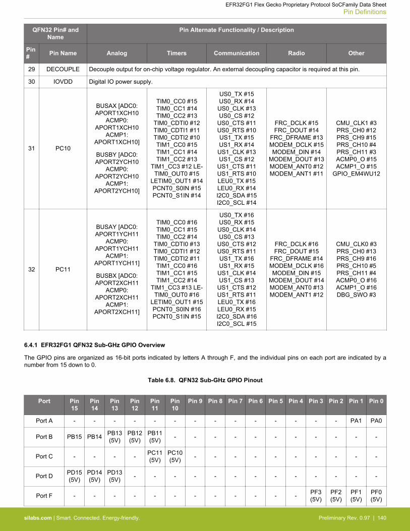
QFN32 Pin# andName
Pin Alternate Functionality / Description
Pin# Pin Name Analog Timers Communication Radio Other
29 DECOUPLE Decouple output for on-chip voltage regulator. An external decoupling capacitor is required at this pin.
30 IOVDD Digital IO power supply.
31 PC10
BUSAX [ADC0:APORT1XCH10
ACMP0:APORT1XCH10
ACMP1:APORT1XCH10]
BUSBY [ADC0:APORT2YCH10
ACMP0:APORT2YCH10
ACMP1:APORT2YCH10]
TIM0_CC0 #15TIM0_CC1 #14TIM0_CC2 #13
TIM0_CDTI0 #12TIM0_CDTI1 #11TIM0_CDTI2 #10TIM1_CC0 #15TIM1_CC1 #14TIM1_CC2 #13
TIM1_CC3 #12 LE-TIM0_OUT0 #15
LETIM0_OUT1 #14PCNT0_S0IN #15PCNT0_S1IN #14
US0_TX #15US0_RX #14
US0_CLK #13US0_CS #12
US0_CTS #11US0_RTS #10US1_TX #15US1_RX #14
US1_CLK #13US1_CS #12
US1_CTS #11US1_RTS #10LEU0_TX #15LEU0_RX #14I2C0_SDA #15I2C0_SCL #14
FRC_DCLK #15FRC_DOUT #14
FRC_DFRAME #13MODEM_DCLK #15MODEM_DIN #14
MODEM_DOUT #13MODEM_ANT0 #12MODEM_ANT1 #11
CMU_CLK1 #3PRS_CH0 #12PRS_CH9 #15PRS_CH10 #4PRS_CH11 #3ACMP0_O #15ACMP1_O #15
GPIO_EM4WU12
32 PC11
BUSAY [ADC0:APORT1YCH11
ACMP0:APORT1YCH11
ACMP1:APORT1YCH11]
BUSBX [ADC0:APORT2XCH11
ACMP0:APORT2XCH11
ACMP1:APORT2XCH11]
TIM0_CC0 #16TIM0_CC1 #15TIM0_CC2 #14
TIM0_CDTI0 #13TIM0_CDTI1 #12TIM0_CDTI2 #11TIM1_CC0 #16TIM1_CC1 #15TIM1_CC2 #14
TIM1_CC3 #13 LE-TIM0_OUT0 #16
LETIM0_OUT1 #15PCNT0_S0IN #16PCNT0_S1IN #15
US0_TX #16US0_RX #15
US0_CLK #14US0_CS #13
US0_CTS #12US0_RTS #11US1_TX #16US1_RX #15
US1_CLK #14US1_CS #13
US1_CTS #12US1_RTS #11LEU0_TX #16LEU0_RX #15I2C0_SDA #16I2C0_SCL #15
FRC_DCLK #16FRC_DOUT #15
FRC_DFRAME #14MODEM_DCLK #16MODEM_DIN #15
MODEM_DOUT #14MODEM_ANT0 #13MODEM_ANT1 #12
CMU_CLK0 #3PRS_CH0 #13PRS_CH9 #16PRS_CH10 #5PRS_CH11 #4ACMP0_O #16ACMP1_O #16DBG_SWO #3
6.4.1 EFR32FG1 QFN32 Sub-GHz GPIO Overview
The GPIO pins are organized as 16-bit ports indicated by letters A through F, and the individual pins on each port are indicated by anumber from 15 down to 0.
Table 6.8. QFN32 Sub-GHz GPIO Pinout
Port Pin15
Pin14
Pin13
Pin12
Pin11
Pin10
Pin 9 Pin 8 Pin 7 Pin 6 Pin 5 Pin 4 Pin 3 Pin 2 Pin 1 Pin 0
Port A - - - - - - - - - - - - - - PA1 PA0
Port B PB15 PB14 PB13(5V)
PB12(5V)
PB11(5V) - - - - - - - - - - -
Port C - - - - PC11(5V)
PC10(5V) - - - - - - - - - -
Port D PD15(5V)
PD14(5V)
PD13(5V) - - - - - - - - - - - - -
Port F - - - - - - - - - - - - PF3(5V)
PF2(5V)
PF1(5V)
PF0(5V)
EFR32FG1 Flex Gecko Proprietary Protocol SoCFamily Data SheetPin Definitions
silabs.com | Smart. Connected. Energy-friendly. Preliminary Rev. 0.97 | 140
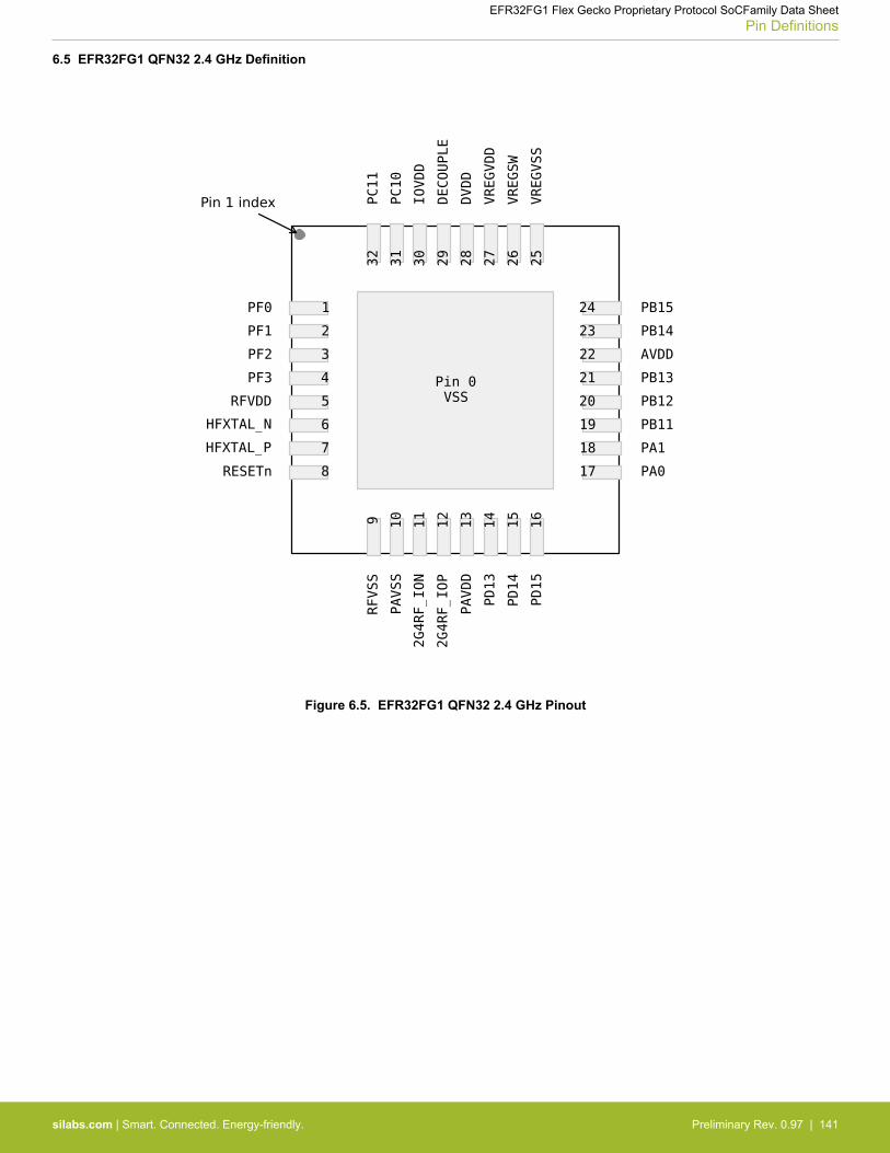
6.5 EFR32FG1 QFN32 2.4 GHz Definition
Figure 6.5. EFR32FG1 QFN32 2.4 GHz Pinout
EFR32FG1 Flex Gecko Proprietary Protocol SoCFamily Data SheetPin Definitions
silabs.com | Smart. Connected. Energy-friendly. Preliminary Rev. 0.97 | 141

Table 6.9. QFN32 2.4 GHz Device Pinout
QFN32 Pin# andName
Pin Alternate Functionality / Description
Pin# Pin Name Analog Timers Communication Radio Other
0 VSS Ground
1 PF0
BUSAX [ADC0:APORT1XCH16
ACMP0:APORT1XCH16
ACMP1:APORT1XCH16]
BUSBY [ADC0:APORT2YCH16
ACMP0:APORT2YCH16
ACMP1:APORT2YCH16]
TIM0_CC0 #24TIM0_CC1 #23TIM0_CC2 #22
TIM0_CDTI0 #21TIM0_CDTI1 #20TIM0_CDTI2 #19TIM1_CC0 #24TIM1_CC1 #23TIM1_CC2 #22
TIM1_CC3 #21 LE-TIM0_OUT0 #24
LETIM0_OUT1 #23PCNT0_S0IN #24PCNT0_S1IN #23
US0_TX #24US0_RX #23
US0_CLK #22US0_CS #21
US0_CTS #20US0_RTS #19US1_TX #24US1_RX #23
US1_CLK #22US1_CS #21
US1_CTS #20US1_RTS #19LEU0_TX #24LEU0_RX #23I2C0_SDA #24I2C0_SCL #23
FRC_DCLK #24FRC_DOUT #23
FRC_DFRAME #22MODEM_DCLK #24MODEM_DIN #23
MODEM_DOUT #22MODEM_ANT0 #21MODEM_ANT1 #20
PRS_CH0 #0PRS_CH1 #7PRS_CH2 #6PRS_CH3 #5
ACMP0_O #24ACMP1_O #24
DBG_SWCLKTCK#0
2 PF1
BUSAY [ADC0:APORT1YCH17
ACMP0:APORT1YCH17
ACMP1:APORT1YCH17]
BUSBX [ADC0:APORT2XCH17
ACMP0:APORT2XCH17
ACMP1:APORT2XCH17]
TIM0_CC0 #25TIM0_CC1 #24TIM0_CC2 #23
TIM0_CDTI0 #22TIM0_CDTI1 #21TIM0_CDTI2 #20TIM1_CC0 #25TIM1_CC1 #24TIM1_CC2 #23
TIM1_CC3 #22 LE-TIM0_OUT0 #25
LETIM0_OUT1 #24PCNT0_S0IN #25PCNT0_S1IN #24
US0_TX #25US0_RX #24
US0_CLK #23US0_CS #22
US0_CTS #21US0_RTS #20US1_TX #25US1_RX #24
US1_CLK #23US1_CS #22
US1_CTS #21US1_RTS #20LEU0_TX #25LEU0_RX #24I2C0_SDA #25I2C0_SCL #24
FRC_DCLK #25FRC_DOUT #24
FRC_DFRAME #23MODEM_DCLK #25MODEM_DIN #24
MODEM_DOUT #23MODEM_ANT0 #22MODEM_ANT1 #21
PRS_CH0 #1PRS_CH1 #0PRS_CH2 #7PRS_CH3 #6
ACMP0_O #25ACMP1_O #25
DBG_SWDIOTMS#0
3 PF2
BUSAX [ADC0:APORT1XCH18
ACMP0:APORT1XCH18
ACMP1:APORT1XCH18]
BUSBY [ADC0:APORT2YCH18
ACMP0:APORT2YCH18
ACMP1:APORT2YCH18]
TIM0_CC0 #26TIM0_CC1 #25TIM0_CC2 #24
TIM0_CDTI0 #23TIM0_CDTI1 #22TIM0_CDTI2 #21TIM1_CC0 #26TIM1_CC1 #25TIM1_CC2 #24
TIM1_CC3 #23 LE-TIM0_OUT0 #26
LETIM0_OUT1 #25PCNT0_S0IN #26PCNT0_S1IN #25
US0_TX #26US0_RX #25
US0_CLK #24US0_CS #23
US0_CTS #22US0_RTS #21US1_TX #26US1_RX #25
US1_CLK #24US1_CS #23
US1_CTS #22US1_RTS #21LEU0_TX #26LEU0_RX #25I2C0_SDA #26I2C0_SCL #25
FRC_DCLK #26FRC_DOUT #25
FRC_DFRAME #24MODEM_DCLK #26MODEM_DIN #25
MODEM_DOUT #24MODEM_ANT0 #23MODEM_ANT1 #22
CMU_CLK0 #6PRS_CH0 #2PRS_CH1 #1PRS_CH2 #0PRS_CH3 #7
ACMP0_O #26ACMP1_O #26DBG_TDO #0DBG_SWO #0
GPIO_EM4WU0
EFR32FG1 Flex Gecko Proprietary Protocol SoCFamily Data SheetPin Definitions
silabs.com | Smart. Connected. Energy-friendly. Preliminary Rev. 0.97 | 142

QFN32 Pin# andName
Pin Alternate Functionality / Description
Pin# Pin Name Analog Timers Communication Radio Other
4 PF3
BUSAY [ADC0:APORT1YCH19
ACMP0:APORT1YCH19
ACMP1:APORT1YCH19]
BUSBX [ADC0:APORT2XCH19
ACMP0:APORT2XCH19
ACMP1:APORT2XCH19]
TIM0_CC0 #27TIM0_CC1 #26TIM0_CC2 #25
TIM0_CDTI0 #24TIM0_CDTI1 #23TIM0_CDTI2 #22TIM1_CC0 #27TIM1_CC1 #26TIM1_CC2 #25
TIM1_CC3 #24 LE-TIM0_OUT0 #27
LETIM0_OUT1 #26PCNT0_S0IN #27PCNT0_S1IN #26
US0_TX #27US0_RX #26
US0_CLK #25US0_CS #24
US0_CTS #23US0_RTS #22US1_TX #27US1_RX #26
US1_CLK #25US1_CS #24
US1_CTS #23US1_RTS #22LEU0_TX #27LEU0_RX #26I2C0_SDA #27I2C0_SCL #26
FRC_DCLK #27FRC_DOUT #26
FRC_DFRAME #25MODEM_DCLK #27MODEM_DIN #26
MODEM_DOUT #25MODEM_ANT0 #24MODEM_ANT1 #23
CMU_CLK1 #6PRS_CH0 #3PRS_CH1 #2PRS_CH2 #1PRS_CH3 #0
ACMP0_O #27ACMP1_O #27DBG_TDI #0
5 RFVDD Radio power supply
6 HFXTAL_N High Frequency Crystal input pin.
7 HFXTAL_P High Frequency Crystal output pin.
8 RESETn Reset input, active low.To apply an external reset source to this pin, it is required to only drive this pin lowduring reset, and let the internal pull-up ensure that reset is released.
9 RFVSS Radio Ground
10 PAVSS Power Amplifier (PA) voltage regulator VSS
11 2G4RF_ION 2.4 GHz Differential RF input/output, negative path.
12 2G4RF_IOP 2.4 GHz Differential RF input/output, positive path.
13 PAVDD Power Amplifier (PA) voltage regulator VDD input
14 PD13
BUSCY [ADC0:APORT3YCH5
ACMP0:APORT3YCH5
ACMP1:APORT3YCH5
IDAC0:APORT1YCH5]
BUSDX [ADC0:APORT4XCH5
ACMP0:APORT4XCH5
ACMP1:APORT4XCH5]
TIM0_CC0 #21TIM0_CC1 #20TIM0_CC2 #19
TIM0_CDTI0 #18TIM0_CDTI1 #17TIM0_CDTI2 #16TIM1_CC0 #21TIM1_CC1 #20TIM1_CC2 #19
TIM1_CC3 #18 LE-TIM0_OUT0 #21
LETIM0_OUT1 #20PCNT0_S0IN #21PCNT0_S1IN #20
US0_TX #21US0_RX #20
US0_CLK #19US0_CS #18
US0_CTS #17US0_RTS #16US1_TX #21US1_RX #20
US1_CLK #19US1_CS #18
US1_CTS #17US1_RTS #16LEU0_TX #21LEU0_RX #20I2C0_SDA #21I2C0_SCL #20
FRC_DCLK #21FRC_DOUT #20
FRC_DFRAME #19MODEM_DCLK #21MODEM_DIN #20
MODEM_DOUT #19MODEM_ANT0 #18MODEM_ANT1 #17
PRS_CH3 #12PRS_CH4 #4PRS_CH5 #3
PRS_CH6 #15ACMP0_O #21ACMP1_O #21
EFR32FG1 Flex Gecko Proprietary Protocol SoCFamily Data SheetPin Definitions
silabs.com | Smart. Connected. Energy-friendly. Preliminary Rev. 0.97 | 143
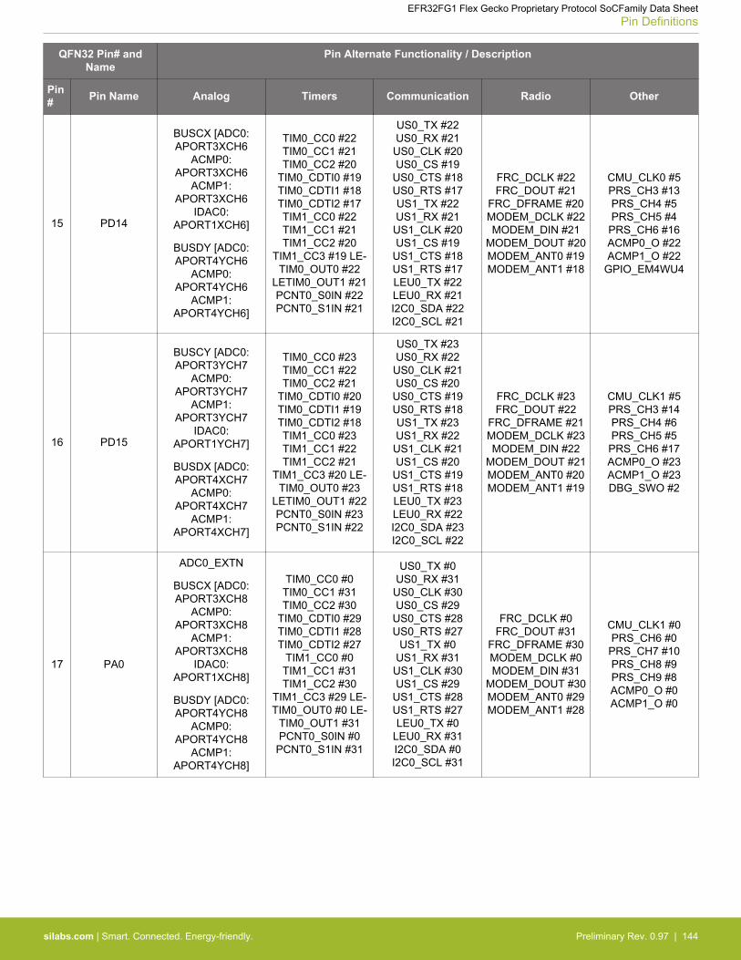
QFN32 Pin# andName
Pin Alternate Functionality / Description
Pin# Pin Name Analog Timers Communication Radio Other
15 PD14
BUSCX [ADC0:APORT3XCH6
ACMP0:APORT3XCH6
ACMP1:APORT3XCH6
IDAC0:APORT1XCH6]
BUSDY [ADC0:APORT4YCH6
ACMP0:APORT4YCH6
ACMP1:APORT4YCH6]
TIM0_CC0 #22TIM0_CC1 #21TIM0_CC2 #20
TIM0_CDTI0 #19TIM0_CDTI1 #18TIM0_CDTI2 #17TIM1_CC0 #22TIM1_CC1 #21TIM1_CC2 #20
TIM1_CC3 #19 LE-TIM0_OUT0 #22
LETIM0_OUT1 #21PCNT0_S0IN #22PCNT0_S1IN #21
US0_TX #22US0_RX #21
US0_CLK #20US0_CS #19
US0_CTS #18US0_RTS #17US1_TX #22US1_RX #21
US1_CLK #20US1_CS #19
US1_CTS #18US1_RTS #17LEU0_TX #22LEU0_RX #21I2C0_SDA #22I2C0_SCL #21
FRC_DCLK #22FRC_DOUT #21
FRC_DFRAME #20MODEM_DCLK #22MODEM_DIN #21
MODEM_DOUT #20MODEM_ANT0 #19MODEM_ANT1 #18
CMU_CLK0 #5PRS_CH3 #13PRS_CH4 #5PRS_CH5 #4
PRS_CH6 #16ACMP0_O #22ACMP1_O #22
GPIO_EM4WU4
16 PD15
BUSCY [ADC0:APORT3YCH7
ACMP0:APORT3YCH7
ACMP1:APORT3YCH7
IDAC0:APORT1YCH7]
BUSDX [ADC0:APORT4XCH7
ACMP0:APORT4XCH7
ACMP1:APORT4XCH7]
TIM0_CC0 #23TIM0_CC1 #22TIM0_CC2 #21
TIM0_CDTI0 #20TIM0_CDTI1 #19TIM0_CDTI2 #18TIM1_CC0 #23TIM1_CC1 #22TIM1_CC2 #21
TIM1_CC3 #20 LE-TIM0_OUT0 #23
LETIM0_OUT1 #22PCNT0_S0IN #23PCNT0_S1IN #22
US0_TX #23US0_RX #22
US0_CLK #21US0_CS #20
US0_CTS #19US0_RTS #18US1_TX #23US1_RX #22
US1_CLK #21US1_CS #20
US1_CTS #19US1_RTS #18LEU0_TX #23LEU0_RX #22I2C0_SDA #23I2C0_SCL #22
FRC_DCLK #23FRC_DOUT #22
FRC_DFRAME #21MODEM_DCLK #23MODEM_DIN #22
MODEM_DOUT #21MODEM_ANT0 #20MODEM_ANT1 #19
CMU_CLK1 #5PRS_CH3 #14PRS_CH4 #6PRS_CH5 #5
PRS_CH6 #17ACMP0_O #23ACMP1_O #23DBG_SWO #2
17 PA0
ADC0_EXTN
BUSCX [ADC0:APORT3XCH8
ACMP0:APORT3XCH8
ACMP1:APORT3XCH8
IDAC0:APORT1XCH8]
BUSDY [ADC0:APORT4YCH8
ACMP0:APORT4YCH8
ACMP1:APORT4YCH8]
TIM0_CC0 #0TIM0_CC1 #31TIM0_CC2 #30
TIM0_CDTI0 #29TIM0_CDTI1 #28TIM0_CDTI2 #27
TIM1_CC0 #0TIM1_CC1 #31TIM1_CC2 #30
TIM1_CC3 #29 LE-TIM0_OUT0 #0 LE-
TIM0_OUT1 #31PCNT0_S0IN #0PCNT0_S1IN #31
US0_TX #0US0_RX #31
US0_CLK #30US0_CS #29
US0_CTS #28US0_RTS #27
US1_TX #0US1_RX #31
US1_CLK #30US1_CS #29
US1_CTS #28US1_RTS #27LEU0_TX #0
LEU0_RX #31I2C0_SDA #0I2C0_SCL #31
FRC_DCLK #0FRC_DOUT #31
FRC_DFRAME #30MODEM_DCLK #0MODEM_DIN #31
MODEM_DOUT #30MODEM_ANT0 #29MODEM_ANT1 #28
CMU_CLK1 #0PRS_CH6 #0
PRS_CH7 #10PRS_CH8 #9PRS_CH9 #8ACMP0_O #0ACMP1_O #0
EFR32FG1 Flex Gecko Proprietary Protocol SoCFamily Data SheetPin Definitions
silabs.com | Smart. Connected. Energy-friendly. Preliminary Rev. 0.97 | 144
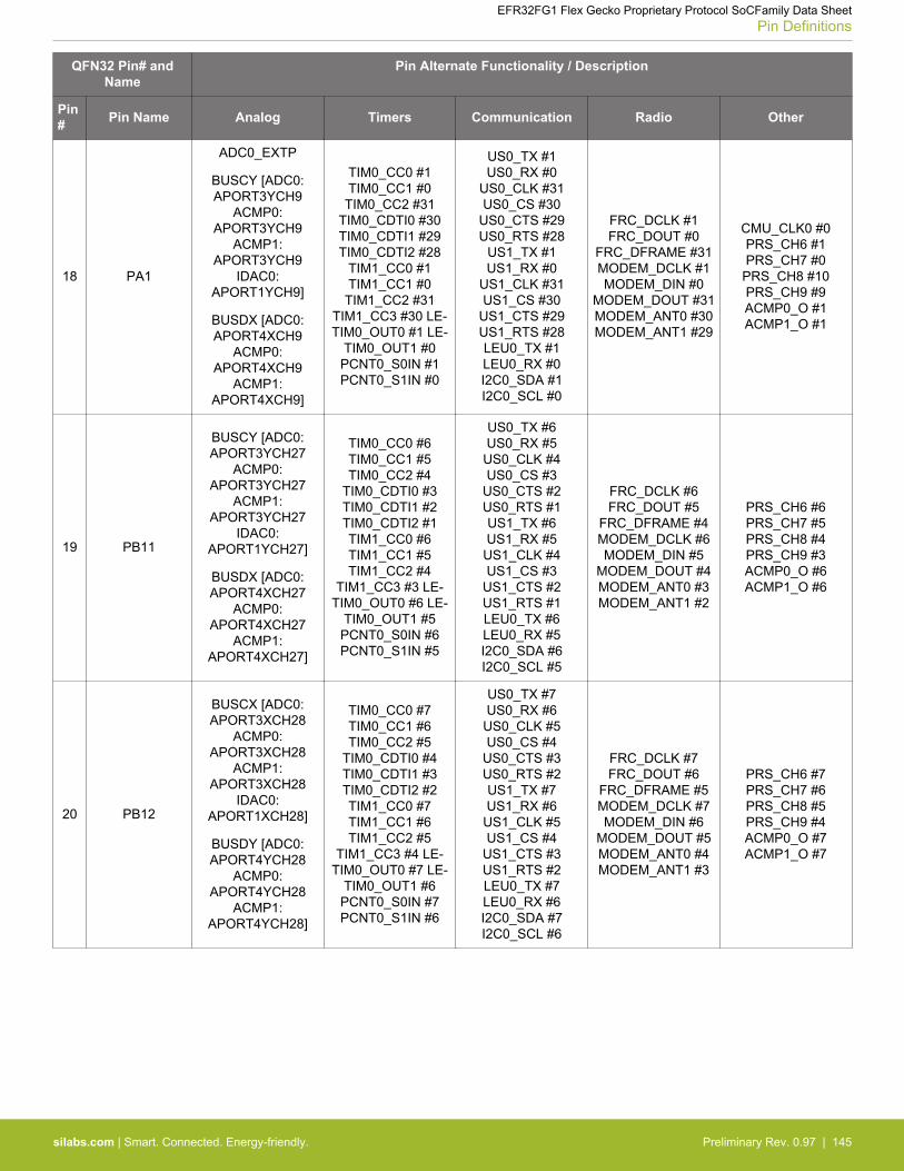
QFN32 Pin# andName
Pin Alternate Functionality / Description
Pin# Pin Name Analog Timers Communication Radio Other
18 PA1
ADC0_EXTP
BUSCY [ADC0:APORT3YCH9
ACMP0:APORT3YCH9
ACMP1:APORT3YCH9
IDAC0:APORT1YCH9]
BUSDX [ADC0:APORT4XCH9
ACMP0:APORT4XCH9
ACMP1:APORT4XCH9]
TIM0_CC0 #1TIM0_CC1 #0TIM0_CC2 #31
TIM0_CDTI0 #30TIM0_CDTI1 #29TIM0_CDTI2 #28
TIM1_CC0 #1TIM1_CC1 #0TIM1_CC2 #31
TIM1_CC3 #30 LE-TIM0_OUT0 #1 LE-
TIM0_OUT1 #0PCNT0_S0IN #1PCNT0_S1IN #0
US0_TX #1US0_RX #0
US0_CLK #31US0_CS #30
US0_CTS #29US0_RTS #28
US1_TX #1US1_RX #0
US1_CLK #31US1_CS #30
US1_CTS #29US1_RTS #28LEU0_TX #1LEU0_RX #0I2C0_SDA #1I2C0_SCL #0
FRC_DCLK #1FRC_DOUT #0
FRC_DFRAME #31MODEM_DCLK #1MODEM_DIN #0
MODEM_DOUT #31MODEM_ANT0 #30MODEM_ANT1 #29
CMU_CLK0 #0PRS_CH6 #1PRS_CH7 #0
PRS_CH8 #10PRS_CH9 #9ACMP0_O #1ACMP1_O #1
19 PB11
BUSCY [ADC0:APORT3YCH27
ACMP0:APORT3YCH27
ACMP1:APORT3YCH27
IDAC0:APORT1YCH27]
BUSDX [ADC0:APORT4XCH27
ACMP0:APORT4XCH27
ACMP1:APORT4XCH27]
TIM0_CC0 #6TIM0_CC1 #5TIM0_CC2 #4
TIM0_CDTI0 #3TIM0_CDTI1 #2TIM0_CDTI2 #1TIM1_CC0 #6TIM1_CC1 #5TIM1_CC2 #4
TIM1_CC3 #3 LE-TIM0_OUT0 #6 LE-
TIM0_OUT1 #5PCNT0_S0IN #6PCNT0_S1IN #5
US0_TX #6US0_RX #5
US0_CLK #4US0_CS #3
US0_CTS #2US0_RTS #1US1_TX #6US1_RX #5
US1_CLK #4US1_CS #3
US1_CTS #2US1_RTS #1LEU0_TX #6LEU0_RX #5I2C0_SDA #6I2C0_SCL #5
FRC_DCLK #6FRC_DOUT #5
FRC_DFRAME #4MODEM_DCLK #6MODEM_DIN #5
MODEM_DOUT #4MODEM_ANT0 #3MODEM_ANT1 #2
PRS_CH6 #6PRS_CH7 #5PRS_CH8 #4PRS_CH9 #3ACMP0_O #6ACMP1_O #6
20 PB12
BUSCX [ADC0:APORT3XCH28
ACMP0:APORT3XCH28
ACMP1:APORT3XCH28
IDAC0:APORT1XCH28]
BUSDY [ADC0:APORT4YCH28
ACMP0:APORT4YCH28
ACMP1:APORT4YCH28]
TIM0_CC0 #7TIM0_CC1 #6TIM0_CC2 #5
TIM0_CDTI0 #4TIM0_CDTI1 #3TIM0_CDTI2 #2TIM1_CC0 #7TIM1_CC1 #6TIM1_CC2 #5
TIM1_CC3 #4 LE-TIM0_OUT0 #7 LE-
TIM0_OUT1 #6PCNT0_S0IN #7PCNT0_S1IN #6
US0_TX #7US0_RX #6
US0_CLK #5US0_CS #4
US0_CTS #3US0_RTS #2US1_TX #7US1_RX #6
US1_CLK #5US1_CS #4
US1_CTS #3US1_RTS #2LEU0_TX #7LEU0_RX #6I2C0_SDA #7I2C0_SCL #6
FRC_DCLK #7FRC_DOUT #6
FRC_DFRAME #5MODEM_DCLK #7MODEM_DIN #6
MODEM_DOUT #5MODEM_ANT0 #4MODEM_ANT1 #3
PRS_CH6 #7PRS_CH7 #6PRS_CH8 #5PRS_CH9 #4ACMP0_O #7ACMP1_O #7
EFR32FG1 Flex Gecko Proprietary Protocol SoCFamily Data SheetPin Definitions
silabs.com | Smart. Connected. Energy-friendly. Preliminary Rev. 0.97 | 145

QFN32 Pin# andName
Pin Alternate Functionality / Description
Pin# Pin Name Analog Timers Communication Radio Other
21 PB13
BUSCY [ADC0:APORT3YCH29
ACMP0:APORT3YCH29
ACMP1:APORT3YCH29
IDAC0:APORT1YCH29]
BUSDX [ADC0:APORT4XCH29
ACMP0:APORT4XCH29
ACMP1:APORT4XCH29]
TIM0_CC0 #8TIM0_CC1 #7TIM0_CC2 #6
TIM0_CDTI0 #5TIM0_CDTI1 #4TIM0_CDTI2 #3TIM1_CC0 #8TIM1_CC1 #7TIM1_CC2 #6
TIM1_CC3 #5 LE-TIM0_OUT0 #8 LE-
TIM0_OUT1 #7PCNT0_S0IN #8PCNT0_S1IN #7
US0_TX #8US0_RX #7
US0_CLK #6US0_CS #5
US0_CTS #4US0_RTS #3US1_TX #8US1_RX #7
US1_CLK #6US1_CS #5
US1_CTS #4US1_RTS #3LEU0_TX #8LEU0_RX #7I2C0_SDA #8I2C0_SCL #7
FRC_DCLK #8FRC_DOUT #7
FRC_DFRAME #6MODEM_DCLK #8MODEM_DIN #7
MODEM_DOUT #6MODEM_ANT0 #5MODEM_ANT1 #4
PRS_CH6 #8PRS_CH7 #7PRS_CH8 #6PRS_CH9 #5ACMP0_O #8ACMP1_O #8DBG_SWO #1
GPIO_EM4WU9
22 AVDD Analog power supply.
23 PB14
LFXTAL_N
BUSCX [ADC0:APORT3XCH30
ACMP0:APORT3XCH30
ACMP1:APORT3XCH30
IDAC0:APORT1XCH30]
BUSDY [ADC0:APORT4YCH30
ACMP0:APORT4YCH30
ACMP1:APORT4YCH30]
TIM0_CC0 #9TIM0_CC1 #8TIM0_CC2 #7
TIM0_CDTI0 #6TIM0_CDTI1 #5TIM0_CDTI2 #4TIM1_CC0 #9TIM1_CC1 #8TIM1_CC2 #7
TIM1_CC3 #6 LE-TIM0_OUT0 #9 LE-
TIM0_OUT1 #8PCNT0_S0IN #9PCNT0_S1IN #8
US0_TX #9US0_RX #8
US0_CLK #7US0_CS #6
US0_CTS #5US0_RTS #4US1_TX #9US1_RX #8
US1_CLK #7US1_CS #6
US1_CTS #5US1_RTS #4LEU0_TX #9LEU0_RX #8I2C0_SDA #9I2C0_SCL #8
FRC_DCLK #9FRC_DOUT #8
FRC_DFRAME #7MODEM_DCLK #9MODEM_DIN #8
MODEM_DOUT #7MODEM_ANT0 #6MODEM_ANT1 #5
CMU_CLK1 #1PRS_CH6 #9PRS_CH7 #8PRS_CH8 #7PRS_CH9 #6ACMP0_O #9ACMP1_O #9
24 PB15
LFXTAL_P
BUSCY [ADC0:APORT3YCH31
ACMP0:APORT3YCH31
ACMP1:APORT3YCH31
IDAC0:APORT1YCH31]
BUSDX [ADC0:APORT4XCH31
ACMP0:APORT4XCH31
ACMP1:APORT4XCH31]
TIM0_CC0 #10TIM0_CC1 #9TIM0_CC2 #8
TIM0_CDTI0 #7TIM0_CDTI1 #6TIM0_CDTI2 #5TIM1_CC0 #10TIM1_CC1 #9TIM1_CC2 #8
TIM1_CC3 #7 LE-TIM0_OUT0 #10
LETIM0_OUT1 #9PCNT0_S0IN #10PCNT0_S1IN #9
US0_TX #10US0_RX #9
US0_CLK #8US0_CS #7
US0_CTS #6US0_RTS #5US1_TX #10US1_RX #9
US1_CLK #8US1_CS #7
US1_CTS #6US1_RTS #5LEU0_TX #10LEU0_RX #9
I2C0_SDA #10I2C0_SCL #9
FRC_DCLK #10FRC_DOUT #9
FRC_DFRAME #8MODEM_DCLK #10
MODEM_DIN #9MODEM_DOUT #8MODEM_ANT0 #7MODEM_ANT1 #6
CMU_CLK0 #1PRS_CH6 #10PRS_CH7 #9PRS_CH8 #8PRS_CH9 #7
ACMP0_O #10ACMP1_O #10
25 VREGVSS Voltage regulator VSS
26 VREGSW DCDC regulator switching node
27 VREGVDD Voltage regulator VDD input
28 DVDD Digital power supply.
EFR32FG1 Flex Gecko Proprietary Protocol SoCFamily Data SheetPin Definitions
silabs.com | Smart. Connected. Energy-friendly. Preliminary Rev. 0.97 | 146
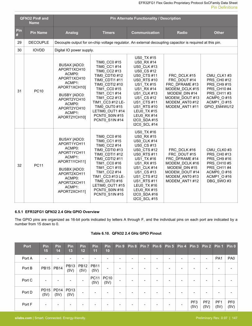
QFN32 Pin# andName
Pin Alternate Functionality / Description
Pin# Pin Name Analog Timers Communication Radio Other
29 DECOUPLE Decouple output for on-chip voltage regulator. An external decoupling capacitor is required at this pin.
30 IOVDD Digital IO power supply.
31 PC10
BUSAX [ADC0:APORT1XCH10
ACMP0:APORT1XCH10
ACMP1:APORT1XCH10]
BUSBY [ADC0:APORT2YCH10
ACMP0:APORT2YCH10
ACMP1:APORT2YCH10]
TIM0_CC0 #15TIM0_CC1 #14TIM0_CC2 #13
TIM0_CDTI0 #12TIM0_CDTI1 #11TIM0_CDTI2 #10TIM1_CC0 #15TIM1_CC1 #14TIM1_CC2 #13
TIM1_CC3 #12 LE-TIM0_OUT0 #15
LETIM0_OUT1 #14PCNT0_S0IN #15PCNT0_S1IN #14
US0_TX #15US0_RX #14
US0_CLK #13US0_CS #12
US0_CTS #11US0_RTS #10US1_TX #15US1_RX #14
US1_CLK #13US1_CS #12
US1_CTS #11US1_RTS #10LEU0_TX #15LEU0_RX #14I2C0_SDA #15I2C0_SCL #14
FRC_DCLK #15FRC_DOUT #14
FRC_DFRAME #13MODEM_DCLK #15MODEM_DIN #14
MODEM_DOUT #13MODEM_ANT0 #12MODEM_ANT1 #11
CMU_CLK1 #3PRS_CH0 #12PRS_CH9 #15PRS_CH10 #4PRS_CH11 #3ACMP0_O #15ACMP1_O #15
GPIO_EM4WU12
32 PC11
BUSAY [ADC0:APORT1YCH11
ACMP0:APORT1YCH11
ACMP1:APORT1YCH11]
BUSBX [ADC0:APORT2XCH11
ACMP0:APORT2XCH11
ACMP1:APORT2XCH11]
TIM0_CC0 #16TIM0_CC1 #15TIM0_CC2 #14
TIM0_CDTI0 #13TIM0_CDTI1 #12TIM0_CDTI2 #11TIM1_CC0 #16TIM1_CC1 #15TIM1_CC2 #14
TIM1_CC3 #13 LE-TIM0_OUT0 #16
LETIM0_OUT1 #15PCNT0_S0IN #16PCNT0_S1IN #15
US0_TX #16US0_RX #15
US0_CLK #14US0_CS #13
US0_CTS #12US0_RTS #11US1_TX #16US1_RX #15
US1_CLK #14US1_CS #13
US1_CTS #12US1_RTS #11LEU0_TX #16LEU0_RX #15I2C0_SDA #16I2C0_SCL #15
FRC_DCLK #16FRC_DOUT #15
FRC_DFRAME #14MODEM_DCLK #16MODEM_DIN #15
MODEM_DOUT #14MODEM_ANT0 #13MODEM_ANT1 #12
CMU_CLK0 #3PRS_CH0 #13PRS_CH9 #16PRS_CH10 #5PRS_CH11 #4ACMP0_O #16ACMP1_O #16DBG_SWO #3
6.5.1 EFR32FG1 QFN32 2.4 GHz GPIO Overview
The GPIO pins are organized as 16-bit ports indicated by letters A through F, and the individual pins on each port are indicated by anumber from 15 down to 0.
Table 6.10. QFN32 2.4 GHz GPIO Pinout
Port Pin15
Pin14
Pin13
Pin12
Pin11
Pin10
Pin 9 Pin 8 Pin 7 Pin 6 Pin 5 Pin 4 Pin 3 Pin 2 Pin 1 Pin 0
Port A - - - - - - - - - - - - - - PA1 PA0
Port B PB15 PB14 PB13(5V)
PB12(5V)
PB11(5V) - - - - - - - - - - -
Port C - - - - PC11(5V)
PC10(5V) - - - - - - - - - -
Port D PD15(5V)
PD14(5V)
PD13(5V) - - - - - - - - - - - - -
Port F - - - - - - - - - - - - PF3(5V)
PF2(5V)
PF1(5V)
PF0(5V)
EFR32FG1 Flex Gecko Proprietary Protocol SoCFamily Data SheetPin Definitions
silabs.com | Smart. Connected. Energy-friendly. Preliminary Rev. 0.97 | 147
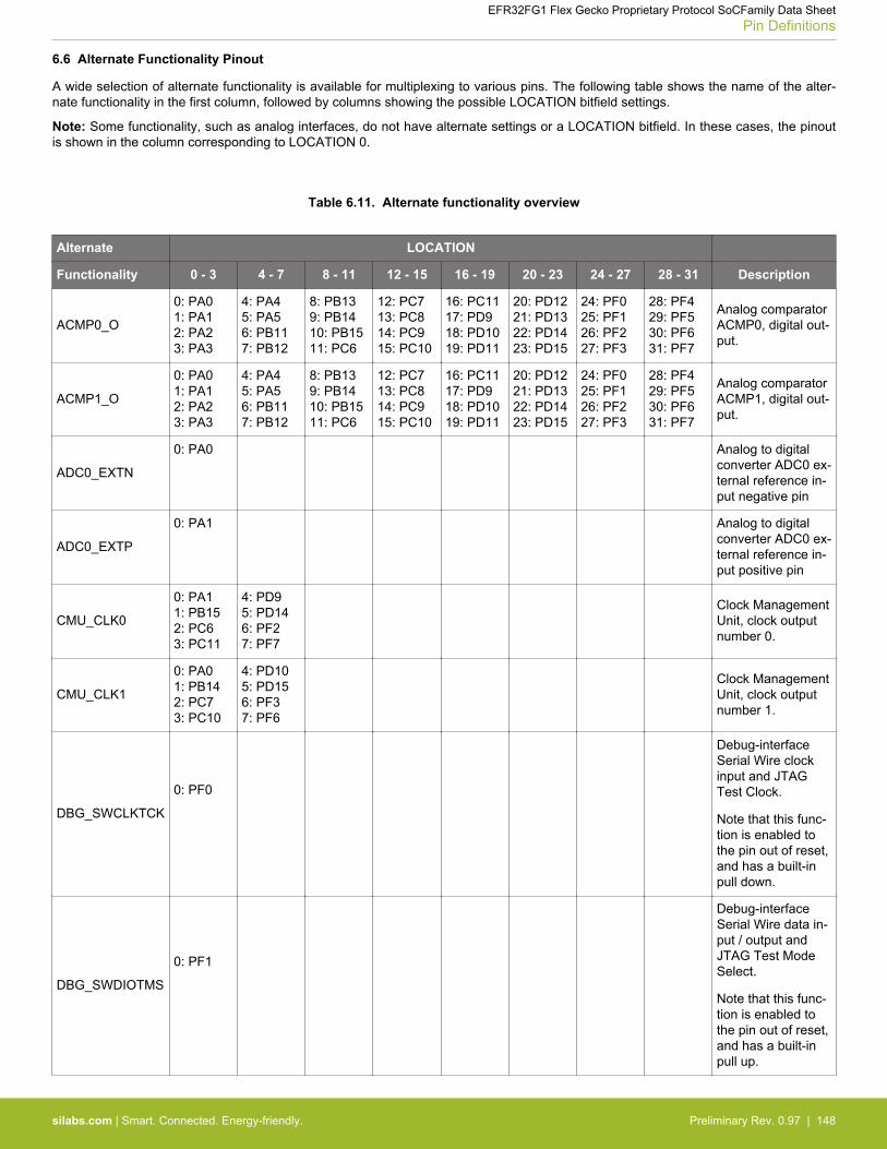
6.6 Alternate Functionality Pinout
A wide selection of alternate functionality is available for multiplexing to various pins. The following table shows the name of the alter-nate functionality in the first column, followed by columns showing the possible LOCATION bitfield settings.
Note: Some functionality, such as analog interfaces, do not have alternate settings or a LOCATION bitfield. In these cases, the pinoutis shown in the column corresponding to LOCATION 0.
Table 6.11. Alternate functionality overview
Alternate LOCATION
Functionality 0 - 3 4 - 7 8 - 11 12 - 15 16 - 19 20 - 23 24 - 27 28 - 31 Description
ACMP0_O
0: PA01: PA12: PA23: PA3
4: PA45: PA56: PB117: PB12
8: PB139: PB1410: PB1511: PC6
12: PC713: PC814: PC915: PC10
16: PC1117: PD918: PD1019: PD11
20: PD1221: PD1322: PD1423: PD15
24: PF025: PF126: PF227: PF3
28: PF429: PF530: PF631: PF7
Analog comparatorACMP0, digital out-put.
ACMP1_O
0: PA01: PA12: PA23: PA3
4: PA45: PA56: PB117: PB12
8: PB139: PB1410: PB1511: PC6
12: PC713: PC814: PC915: PC10
16: PC1117: PD918: PD1019: PD11
20: PD1221: PD1322: PD1423: PD15
24: PF025: PF126: PF227: PF3
28: PF429: PF530: PF631: PF7
Analog comparatorACMP1, digital out-put.
ADC0_EXTN
0: PA0 Analog to digitalconverter ADC0 ex-ternal reference in-put negative pin
ADC0_EXTP
0: PA1 Analog to digitalconverter ADC0 ex-ternal reference in-put positive pin
CMU_CLK0
0: PA11: PB152: PC63: PC11
4: PD95: PD146: PF27: PF7
Clock ManagementUnit, clock outputnumber 0.
CMU_CLK1
0: PA01: PB142: PC73: PC10
4: PD105: PD156: PF37: PF6
Clock ManagementUnit, clock outputnumber 1.
DBG_SWCLKTCK
0: PF0
Debug-interfaceSerial Wire clockinput and JTAGTest Clock.
Note that this func-tion is enabled tothe pin out of reset,and has a built-inpull down.
DBG_SWDIOTMS
0: PF1
Debug-interfaceSerial Wire data in-put / output andJTAG Test ModeSelect.
Note that this func-tion is enabled tothe pin out of reset,and has a built-inpull up.
EFR32FG1 Flex Gecko Proprietary Protocol SoCFamily Data SheetPin Definitions
silabs.com | Smart. Connected. Energy-friendly. Preliminary Rev. 0.97 | 148
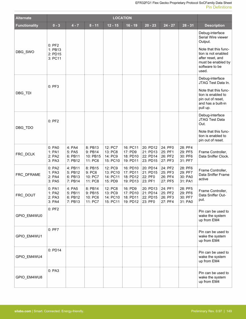
Alternate LOCATION
Functionality 0 - 3 4 - 7 8 - 11 12 - 15 16 - 19 20 - 23 24 - 27 28 - 31 Description
DBG_SWO
0: PF21: PB132: PD153: PC11
Debug-interfaceSerial Wire viewerOutput.
Note that this func-tion is not enabledafter reset, andmust be enabled bysoftware to beused.
DBG_TDI
0: PF3
Debug-interfaceJTAG Test Data In.
Note that this func-tion is enabled topin out of reset,and has a built-inpull up.
DBG_TDO
0: PF2Debug-interfaceJTAG Test DataOut.
Note that this func-tion is enabled topin out of reset.
FRC_DCLK
0: PA01: PA12: PA23: PA3
4: PA45: PA56: PB117: PB12
8: PB139: PB1410: PB1511: PC6
12: PC713: PC814: PC915: PC10
16: PC1117: PD918: PD1019: PD11
20: PD1221: PD1322: PD1423: PD15
24: PF025: PF126: PF227: PF3
28: PF429: PF530: PF631: PF7
Frame Controller,Data Sniffer Clock.
FRC_DFRAME
0: PA21: PA32: PA43: PA5
4: PB115: PB126: PB137: PB14
8: PB159: PC610: PC711: PC8
12: PC913: PC1014: PC1115: PD9
16: PD1017: PD1118: PD1219: PD13
20: PD1421: PD1522: PF023: PF1
24: PF225: PF326: PF427: PF5
28: PF629: PF730: PA031: PA1
Frame Controller,Data Sniffer Frameactive
FRC_DOUT
0: PA11: PA22: PA33: PA4
4: PA55: PB116: PB127: PB13
8: PB149: PB1510: PC611: PC7
12: PC813: PC914: PC1015: PC11
16: PD917: PD1018: PD1119: PD12
20: PD1321: PD1422: PD1523: PF0
24: PF125: PF226: PF327: PF4
28: PF529: PF630: PF731: PA0
Frame Controller,Data Sniffer Out-put.
GPIO_EM4WU0
0: PF2 Pin can be used towake the systemup from EM4
GPIO_EM4WU1
0: PF7 Pin can be used towake the systemup from EM4
GPIO_EM4WU4
0: PD14 Pin can be used towake the systemup from EM4
GPIO_EM4WU8
0: PA3 Pin can be used towake the systemup from EM4
EFR32FG1 Flex Gecko Proprietary Protocol SoCFamily Data SheetPin Definitions
silabs.com | Smart. Connected. Energy-friendly. Preliminary Rev. 0.97 | 149
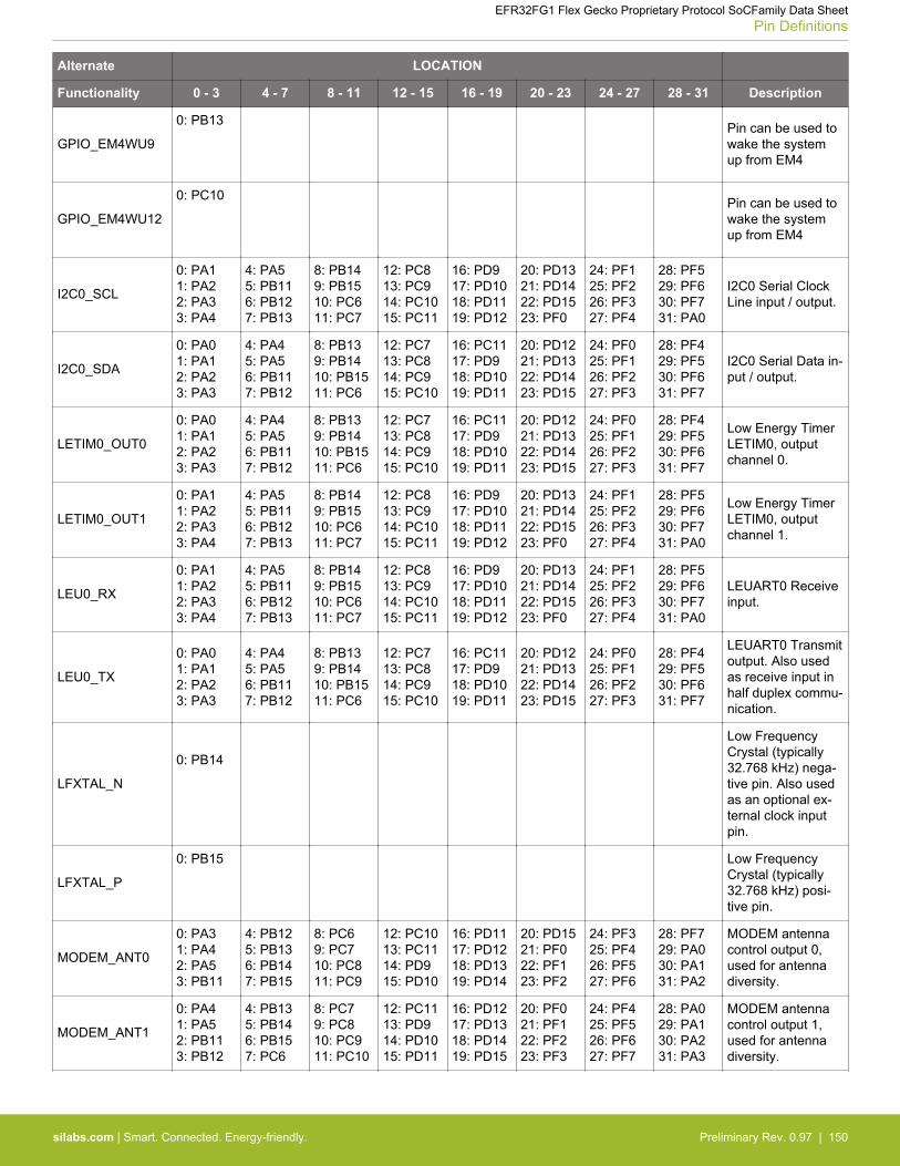
Alternate LOCATION
Functionality 0 - 3 4 - 7 8 - 11 12 - 15 16 - 19 20 - 23 24 - 27 28 - 31 Description
GPIO_EM4WU9
0: PB13 Pin can be used towake the systemup from EM4
GPIO_EM4WU12
0: PC10 Pin can be used towake the systemup from EM4
I2C0_SCL
0: PA11: PA22: PA33: PA4
4: PA55: PB116: PB127: PB13
8: PB149: PB1510: PC611: PC7
12: PC813: PC914: PC1015: PC11
16: PD917: PD1018: PD1119: PD12
20: PD1321: PD1422: PD1523: PF0
24: PF125: PF226: PF327: PF4
28: PF529: PF630: PF731: PA0
I2C0 Serial ClockLine input / output.
I2C0_SDA
0: PA01: PA12: PA23: PA3
4: PA45: PA56: PB117: PB12
8: PB139: PB1410: PB1511: PC6
12: PC713: PC814: PC915: PC10
16: PC1117: PD918: PD1019: PD11
20: PD1221: PD1322: PD1423: PD15
24: PF025: PF126: PF227: PF3
28: PF429: PF530: PF631: PF7
I2C0 Serial Data in-put / output.
LETIM0_OUT0
0: PA01: PA12: PA23: PA3
4: PA45: PA56: PB117: PB12
8: PB139: PB1410: PB1511: PC6
12: PC713: PC814: PC915: PC10
16: PC1117: PD918: PD1019: PD11
20: PD1221: PD1322: PD1423: PD15
24: PF025: PF126: PF227: PF3
28: PF429: PF530: PF631: PF7
Low Energy TimerLETIM0, outputchannel 0.
LETIM0_OUT1
0: PA11: PA22: PA33: PA4
4: PA55: PB116: PB127: PB13
8: PB149: PB1510: PC611: PC7
12: PC813: PC914: PC1015: PC11
16: PD917: PD1018: PD1119: PD12
20: PD1321: PD1422: PD1523: PF0
24: PF125: PF226: PF327: PF4
28: PF529: PF630: PF731: PA0
Low Energy TimerLETIM0, outputchannel 1.
LEU0_RX
0: PA11: PA22: PA33: PA4
4: PA55: PB116: PB127: PB13
8: PB149: PB1510: PC611: PC7
12: PC813: PC914: PC1015: PC11
16: PD917: PD1018: PD1119: PD12
20: PD1321: PD1422: PD1523: PF0
24: PF125: PF226: PF327: PF4
28: PF529: PF630: PF731: PA0
LEUART0 Receiveinput.
LEU0_TX
0: PA01: PA12: PA23: PA3
4: PA45: PA56: PB117: PB12
8: PB139: PB1410: PB1511: PC6
12: PC713: PC814: PC915: PC10
16: PC1117: PD918: PD1019: PD11
20: PD1221: PD1322: PD1423: PD15
24: PF025: PF126: PF227: PF3
28: PF429: PF530: PF631: PF7
LEUART0 Transmitoutput. Also usedas receive input inhalf duplex commu-nication.
LFXTAL_N
0: PB14
Low FrequencyCrystal (typically32.768 kHz) nega-tive pin. Also usedas an optional ex-ternal clock inputpin.
LFXTAL_P
0: PB15 Low FrequencyCrystal (typically32.768 kHz) posi-tive pin.
MODEM_ANT0
0: PA31: PA42: PA53: PB11
4: PB125: PB136: PB147: PB15
8: PC69: PC710: PC811: PC9
12: PC1013: PC1114: PD915: PD10
16: PD1117: PD1218: PD1319: PD14
20: PD1521: PF022: PF123: PF2
24: PF325: PF426: PF527: PF6
28: PF729: PA030: PA131: PA2
MODEM antennacontrol output 0,used for antennadiversity.
MODEM_ANT1
0: PA41: PA52: PB113: PB12
4: PB135: PB146: PB157: PC6
8: PC79: PC810: PC911: PC10
12: PC1113: PD914: PD1015: PD11
16: PD1217: PD1318: PD1419: PD15
20: PF021: PF122: PF223: PF3
24: PF425: PF526: PF627: PF7
28: PA029: PA130: PA231: PA3
MODEM antennacontrol output 1,used for antennadiversity.
EFR32FG1 Flex Gecko Proprietary Protocol SoCFamily Data SheetPin Definitions
silabs.com | Smart. Connected. Energy-friendly. Preliminary Rev. 0.97 | 150
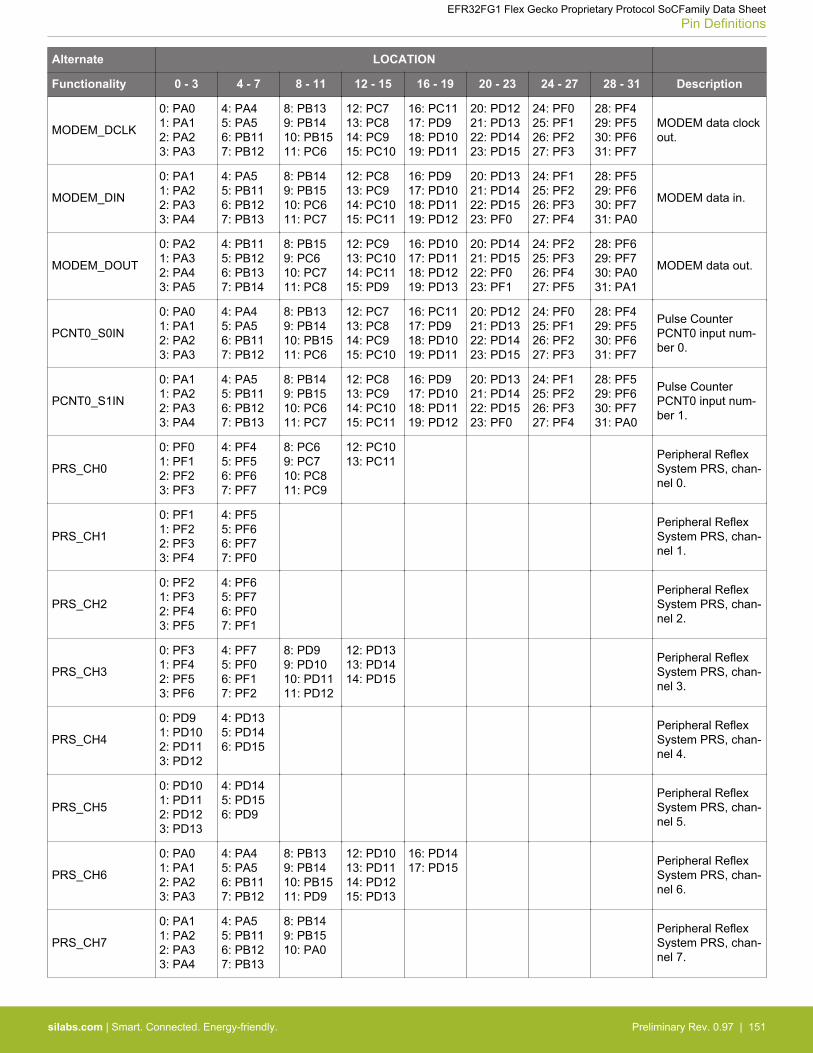
Alternate LOCATION
Functionality 0 - 3 4 - 7 8 - 11 12 - 15 16 - 19 20 - 23 24 - 27 28 - 31 Description
MODEM_DCLK
0: PA01: PA12: PA23: PA3
4: PA45: PA56: PB117: PB12
8: PB139: PB1410: PB1511: PC6
12: PC713: PC814: PC915: PC10
16: PC1117: PD918: PD1019: PD11
20: PD1221: PD1322: PD1423: PD15
24: PF025: PF126: PF227: PF3
28: PF429: PF530: PF631: PF7
MODEM data clockout.
MODEM_DIN
0: PA11: PA22: PA33: PA4
4: PA55: PB116: PB127: PB13
8: PB149: PB1510: PC611: PC7
12: PC813: PC914: PC1015: PC11
16: PD917: PD1018: PD1119: PD12
20: PD1321: PD1422: PD1523: PF0
24: PF125: PF226: PF327: PF4
28: PF529: PF630: PF731: PA0
MODEM data in.
MODEM_DOUT
0: PA21: PA32: PA43: PA5
4: PB115: PB126: PB137: PB14
8: PB159: PC610: PC711: PC8
12: PC913: PC1014: PC1115: PD9
16: PD1017: PD1118: PD1219: PD13
20: PD1421: PD1522: PF023: PF1
24: PF225: PF326: PF427: PF5
28: PF629: PF730: PA031: PA1
MODEM data out.
PCNT0_S0IN
0: PA01: PA12: PA23: PA3
4: PA45: PA56: PB117: PB12
8: PB139: PB1410: PB1511: PC6
12: PC713: PC814: PC915: PC10
16: PC1117: PD918: PD1019: PD11
20: PD1221: PD1322: PD1423: PD15
24: PF025: PF126: PF227: PF3
28: PF429: PF530: PF631: PF7
Pulse CounterPCNT0 input num-ber 0.
PCNT0_S1IN
0: PA11: PA22: PA33: PA4
4: PA55: PB116: PB127: PB13
8: PB149: PB1510: PC611: PC7
12: PC813: PC914: PC1015: PC11
16: PD917: PD1018: PD1119: PD12
20: PD1321: PD1422: PD1523: PF0
24: PF125: PF226: PF327: PF4
28: PF529: PF630: PF731: PA0
Pulse CounterPCNT0 input num-ber 1.
PRS_CH0
0: PF01: PF12: PF23: PF3
4: PF45: PF56: PF67: PF7
8: PC69: PC710: PC811: PC9
12: PC1013: PC11 Peripheral Reflex
System PRS, chan-nel 0.
PRS_CH1
0: PF11: PF22: PF33: PF4
4: PF55: PF66: PF77: PF0
Peripheral ReflexSystem PRS, chan-nel 1.
PRS_CH2
0: PF21: PF32: PF43: PF5
4: PF65: PF76: PF07: PF1
Peripheral ReflexSystem PRS, chan-nel 2.
PRS_CH3
0: PF31: PF42: PF53: PF6
4: PF75: PF06: PF17: PF2
8: PD99: PD1010: PD1111: PD12
12: PD1313: PD1414: PD15
Peripheral ReflexSystem PRS, chan-nel 3.
PRS_CH4
0: PD91: PD102: PD113: PD12
4: PD135: PD146: PD15
Peripheral ReflexSystem PRS, chan-nel 4.
PRS_CH5
0: PD101: PD112: PD123: PD13
4: PD145: PD156: PD9
Peripheral ReflexSystem PRS, chan-nel 5.
PRS_CH6
0: PA01: PA12: PA23: PA3
4: PA45: PA56: PB117: PB12
8: PB139: PB1410: PB1511: PD9
12: PD1013: PD1114: PD1215: PD13
16: PD1417: PD15 Peripheral Reflex
System PRS, chan-nel 6.
PRS_CH7
0: PA11: PA22: PA33: PA4
4: PA55: PB116: PB127: PB13
8: PB149: PB1510: PA0
Peripheral ReflexSystem PRS, chan-nel 7.
EFR32FG1 Flex Gecko Proprietary Protocol SoCFamily Data SheetPin Definitions
silabs.com | Smart. Connected. Energy-friendly. Preliminary Rev. 0.97 | 151
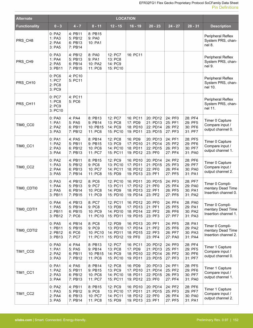
Alternate LOCATION
Functionality 0 - 3 4 - 7 8 - 11 12 - 15 16 - 19 20 - 23 24 - 27 28 - 31 Description
PRS_CH8
0: PA21: PA32: PA43: PA5
4: PB115: PB126: PB137: PB14
8: PB159: PA010: PA1
Peripheral ReflexSystem PRS, chan-nel 8.
PRS_CH9
0: PA31: PA42: PA53: PB11
4: PB125: PB136: PB147: PB15
8: PA09: PA110: PA211: PC6
12: PC713: PC814: PC915: PC10
16: PC11 Peripheral ReflexSystem PRS, chan-nel 9.
PRS_CH10
0: PC61: PC72: PC83: PC9
4: PC105: PC11 Peripheral Reflex
System PRS, chan-nel 10.
PRS_CH11
0: PC71: PC82: PC93: PC10
4: PC115: PC6 Peripheral Reflex
System PRS, chan-nel 11.
TIM0_CC0
0: PA01: PA12: PA23: PA3
4: PA45: PA56: PB117: PB12
8: PB139: PB1410: PB1511: PC6
12: PC713: PC814: PC915: PC10
16: PC1117: PD918: PD1019: PD11
20: PD1221: PD1322: PD1423: PD15
24: PF025: PF126: PF227: PF3
28: PF429: PF530: PF631: PF7
Timer 0 CaptureCompare input /output channel 0.
TIM0_CC1
0: PA11: PA22: PA33: PA4
4: PA55: PB116: PB127: PB13
8: PB149: PB1510: PC611: PC7
12: PC813: PC914: PC1015: PC11
16: PD917: PD1018: PD1119: PD12
20: PD1321: PD1422: PD1523: PF0
24: PF125: PF226: PF327: PF4
28: PF529: PF630: PF731: PA0
Timer 0 CaptureCompare input /output channel 1.
TIM0_CC2
0: PA21: PA32: PA43: PA5
4: PB115: PB126: PB137: PB14
8: PB159: PC610: PC711: PC8
12: PC913: PC1014: PC1115: PD9
16: PD1017: PD1118: PD1219: PD13
20: PD1421: PD1522: PF023: PF1
24: PF225: PF326: PF427: PF5
28: PF629: PF730: PA031: PA1
Timer 0 CaptureCompare input /output channel 2.
TIM0_CDTI0
0: PA31: PA42: PA53: PB11
4: PB125: PB136: PB147: PB15
8: PC69: PC710: PC811: PC9
12: PC1013: PC1114: PD915: PD10
16: PD1117: PD1218: PD1319: PD14
20: PD1521: PF022: PF123: PF2
24: PF325: PF426: PF527: PF6
28: PF729: PA030: PA131: PA2
Timer 0 Compli-mentary Dead TimeInsertion channel 0.
TIM0_CDTI1
0: PA41: PA52: PB113: PB12
4: PB135: PB146: PB157: PC6
8: PC79: PC810: PC911: PC10
12: PC1113: PD914: PD1015: PD11
16: PD1217: PD1318: PD1419: PD15
20: PF021: PF122: PF223: PF3
24: PF425: PF526: PF627: PF7
28: PA029: PA130: PA231: PA3
Timer 0 Compli-mentary Dead TimeInsertion channel 1.
TIM0_CDTI2
0: PA51: PB112: PB123: PB13
4: PB145: PB156: PC67: PC7
8: PC89: PC910: PC1011: PC11
12: PD913: PD1014: PD1115: PD12
16: PD1317: PD1418: PD1519: PF0
20: PF121: PF222: PF323: PF4
24: PF525: PF626: PF727: PA0
28: PA129: PA230: PA331: PA4
Timer 0 Compli-mentary Dead TimeInsertion channel 2.
TIM1_CC0
0: PA01: PA12: PA23: PA3
4: PA45: PA56: PB117: PB12
8: PB139: PB1410: PB1511: PC6
12: PC713: PC814: PC915: PC10
16: PC1117: PD918: PD1019: PD11
20: PD1221: PD1322: PD1423: PD15
24: PF025: PF126: PF227: PF3
28: PF429: PF530: PF631: PF7
Timer 1 CaptureCompare input /output channel 0.
TIM1_CC1
0: PA11: PA22: PA33: PA4
4: PA55: PB116: PB127: PB13
8: PB149: PB1510: PC611: PC7
12: PC813: PC914: PC1015: PC11
16: PD917: PD1018: PD1119: PD12
20: PD1321: PD1422: PD1523: PF0
24: PF125: PF226: PF327: PF4
28: PF529: PF630: PF731: PA0
Timer 1 CaptureCompare input /output channel 1.
TIM1_CC2
0: PA21: PA32: PA43: PA5
4: PB115: PB126: PB137: PB14
8: PB159: PC610: PC711: PC8
12: PC913: PC1014: PC1115: PD9
16: PD1017: PD1118: PD1219: PD13
20: PD1421: PD1522: PF023: PF1
24: PF225: PF326: PF427: PF5
28: PF629: PF730: PA031: PA1
Timer 1 CaptureCompare input /output channel 2.
EFR32FG1 Flex Gecko Proprietary Protocol SoCFamily Data SheetPin Definitions
silabs.com | Smart. Connected. Energy-friendly. Preliminary Rev. 0.97 | 152
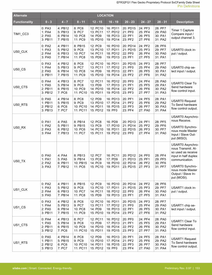
Alternate LOCATION
Functionality 0 - 3 4 - 7 8 - 11 12 - 15 16 - 19 20 - 23 24 - 27 28 - 31 Description
TIM1_CC3
0: PA31: PA42: PA53: PB11
4: PB125: PB136: PB147: PB15
8: PC69: PC710: PC811: PC9
12: PC1013: PC1114: PD915: PD10
16: PD1117: PD1218: PD1319: PD14
20: PD1521: PF022: PF123: PF2
24: PF325: PF426: PF527: PF6
28: PF729: PA030: PA131: PA2
Timer 1 CaptureCompare input /output channel 3.
US0_CLK
0: PA21: PA32: PA43: PA5
4: PB115: PB126: PB137: PB14
8: PB159: PC610: PC711: PC8
12: PC913: PC1014: PC1115: PD9
16: PD1017: PD1118: PD1219: PD13
20: PD1421: PD1522: PF023: PF1
24: PF225: PF326: PF427: PF5
28: PF629: PF730: PA031: PA1
USART0 clock in-put / output.
US0_CS
0: PA31: PA42: PA53: PB11
4: PB125: PB136: PB147: PB15
8: PC69: PC710: PC811: PC9
12: PC1013: PC1114: PD915: PD10
16: PD1117: PD1218: PD1319: PD14
20: PD1521: PF022: PF123: PF2
24: PF325: PF426: PF527: PF6
28: PF729: PA030: PA131: PA2
USART0 chip se-lect input / output.
US0_CTS
0: PA41: PA52: PB113: PB12
4: PB135: PB146: PB157: PC6
8: PC79: PC810: PC911: PC10
12: PC1113: PD914: PD1015: PD11
16: PD1217: PD1318: PD1419: PD15
20: PF021: PF122: PF223: PF3
24: PF425: PF526: PF627: PF7
28: PA029: PA130: PA231: PA3
USART0 Clear ToSend hardwareflow control input.
US0_RTS
0: PA51: PB112: PB123: PB13
4: PB145: PB156: PC67: PC7
8: PC89: PC910: PC1011: PC11
12: PD913: PD1014: PD1115: PD12
16: PD1317: PD1418: PD1519: PF0
20: PF121: PF222: PF323: PF4
24: PF525: PF626: PF727: PA0
28: PA129: PA230: PA331: PA4
USART0 RequestTo Send hardwareflow control output.
US0_RX
0: PA11: PA22: PA33: PA4
4: PA55: PB116: PB127: PB13
8: PB149: PB1510: PC611: PC7
12: PC813: PC914: PC1015: PC11
16: PD917: PD1018: PD1119: PD12
20: PD1321: PD1422: PD1523: PF0
24: PF125: PF226: PF327: PF4
28: PF529: PF630: PF731: PA0
USART0 Asynchro-nous Receive.
USART0 Synchro-nous mode MasterInput / Slave Out-put (MISO).
US0_TX
0: PA01: PA12: PA23: PA3
4: PA45: PA56: PB117: PB12
8: PB139: PB1410: PB1511: PC6
12: PC713: PC814: PC915: PC10
16: PC1117: PD918: PD1019: PD11
20: PD1221: PD1322: PD1423: PD15
24: PF025: PF126: PF227: PF3
28: PF429: PF530: PF631: PF7
USART0 Asynchro-nous Transmit. Al-so used as receiveinput in half duplexcommunication.
USART0 Synchro-nous mode MasterOutput / Slave In-put (MOSI).
US1_CLK
0: PA21: PA32: PA43: PA5
4: PB115: PB126: PB137: PB14
8: PB159: PC610: PC711: PC8
12: PC913: PC1014: PC1115: PD9
16: PD1017: PD1118: PD1219: PD13
20: PD1421: PD1522: PF023: PF1
24: PF225: PF326: PF427: PF5
28: PF629: PF730: PA031: PA1
USART1 clock in-put / output.
US1_CS
0: PA31: PA42: PA53: PB11
4: PB125: PB136: PB147: PB15
8: PC69: PC710: PC811: PC9
12: PC1013: PC1114: PD915: PD10
16: PD1117: PD1218: PD1319: PD14
20: PD1521: PF022: PF123: PF2
24: PF325: PF426: PF527: PF6
28: PF729: PA030: PA131: PA2
USART1 chip se-lect input / output.
US1_CTS
0: PA41: PA52: PB113: PB12
4: PB135: PB146: PB157: PC6
8: PC79: PC810: PC911: PC10
12: PC1113: PD914: PD1015: PD11
16: PD1217: PD1318: PD1419: PD15
20: PF021: PF122: PF223: PF3
24: PF425: PF526: PF627: PF7
28: PA029: PA130: PA231: PA3
USART1 Clear ToSend hardwareflow control input.
US1_RTS
0: PA51: PB112: PB123: PB13
4: PB145: PB156: PC67: PC7
8: PC89: PC910: PC1011: PC11
12: PD913: PD1014: PD1115: PD12
16: PD1317: PD1418: PD1519: PF0
20: PF121: PF222: PF323: PF4
24: PF525: PF626: PF727: PA0
28: PA129: PA230: PA331: PA4
USART1 RequestTo Send hardwareflow control output.
EFR32FG1 Flex Gecko Proprietary Protocol SoCFamily Data SheetPin Definitions
silabs.com | Smart. Connected. Energy-friendly. Preliminary Rev. 0.97 | 153
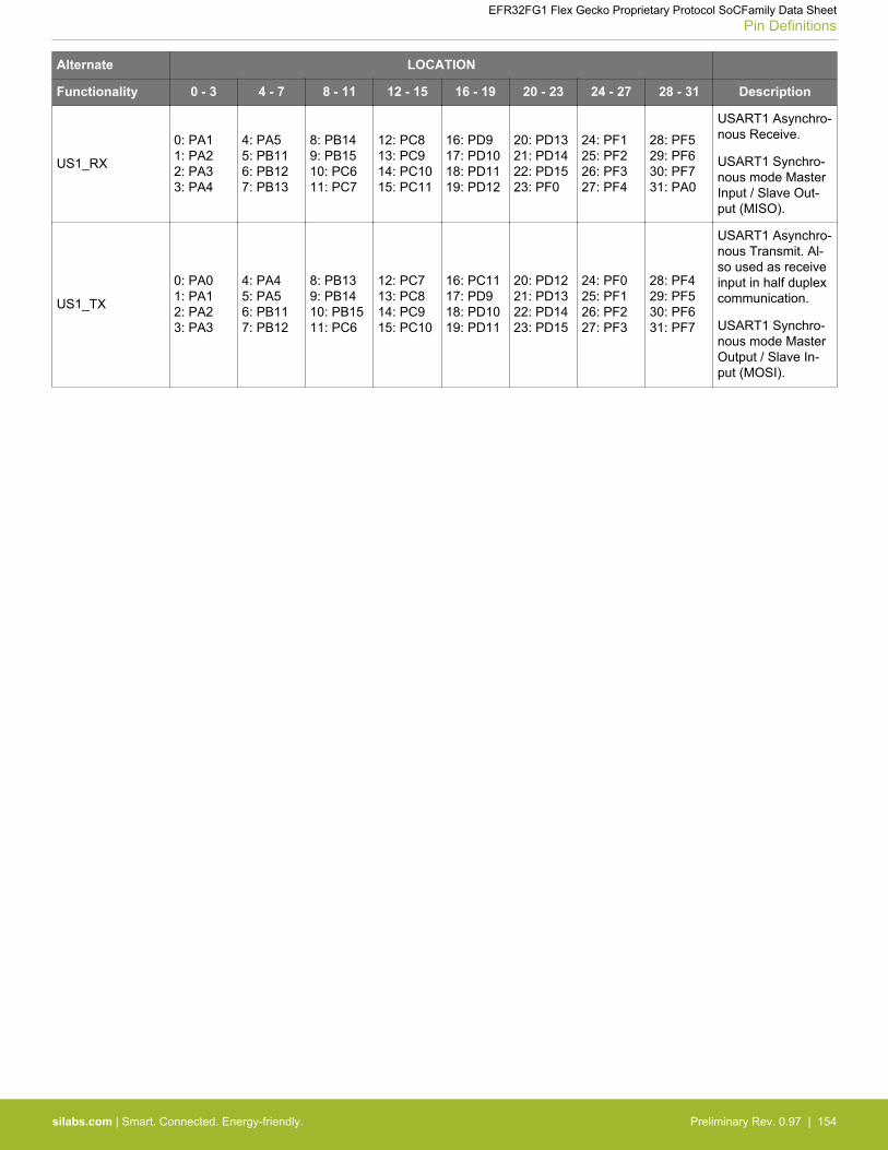
Alternate LOCATION
Functionality 0 - 3 4 - 7 8 - 11 12 - 15 16 - 19 20 - 23 24 - 27 28 - 31 Description
US1_RX
0: PA11: PA22: PA33: PA4
4: PA55: PB116: PB127: PB13
8: PB149: PB1510: PC611: PC7
12: PC813: PC914: PC1015: PC11
16: PD917: PD1018: PD1119: PD12
20: PD1321: PD1422: PD1523: PF0
24: PF125: PF226: PF327: PF4
28: PF529: PF630: PF731: PA0
USART1 Asynchro-nous Receive.
USART1 Synchro-nous mode MasterInput / Slave Out-put (MISO).
US1_TX
0: PA01: PA12: PA23: PA3
4: PA45: PA56: PB117: PB12
8: PB139: PB1410: PB1511: PC6
12: PC713: PC814: PC915: PC10
16: PC1117: PD918: PD1019: PD11
20: PD1221: PD1322: PD1423: PD15
24: PF025: PF126: PF227: PF3
28: PF429: PF530: PF631: PF7
USART1 Asynchro-nous Transmit. Al-so used as receiveinput in half duplexcommunication.
USART1 Synchro-nous mode MasterOutput / Slave In-put (MOSI).
EFR32FG1 Flex Gecko Proprietary Protocol SoCFamily Data SheetPin Definitions
silabs.com | Smart. Connected. Energy-friendly. Preliminary Rev. 0.97 | 154
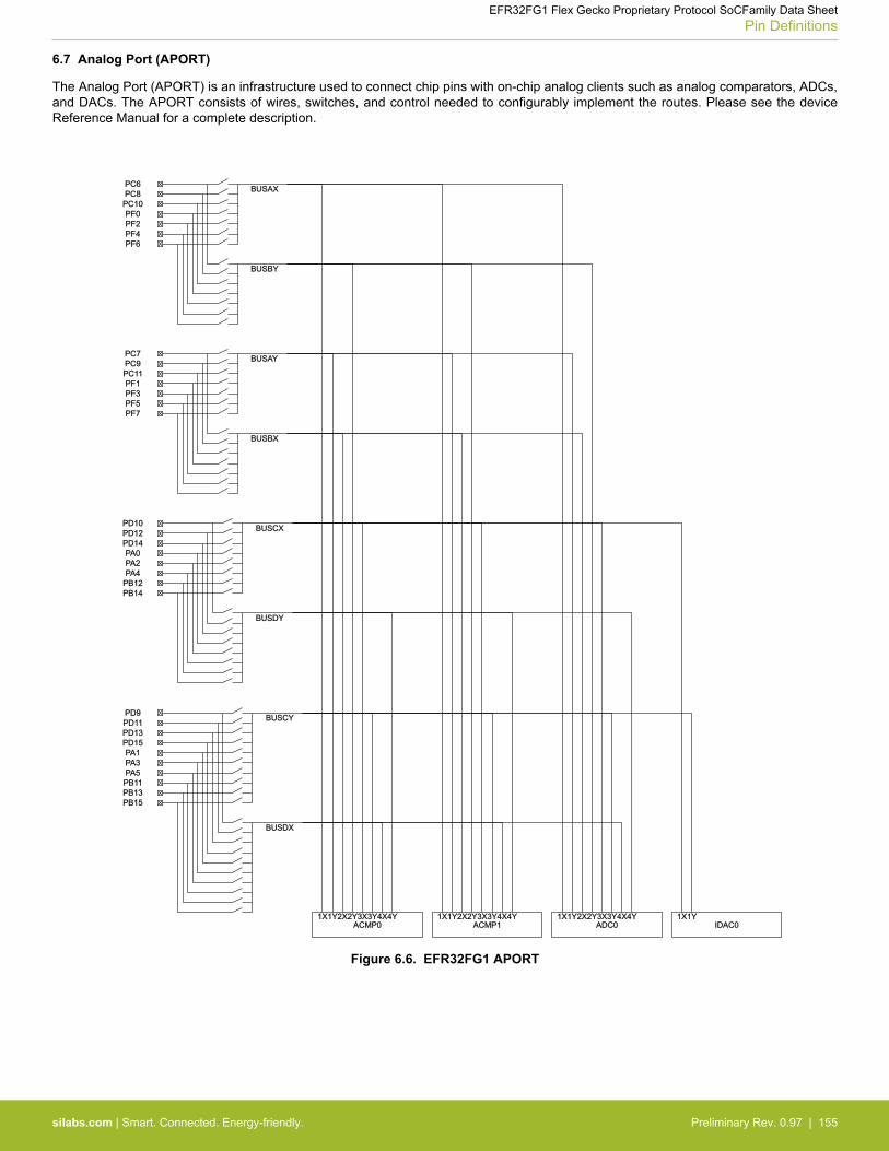
6.7 Analog Port (APORT)
The Analog Port (APORT) is an infrastructure used to connect chip pins with on-chip analog clients such as analog comparators, ADCs,and DACs. The APORT consists of wires, switches, and control needed to configurably implement the routes. Please see the deviceReference Manual for a complete description.
PC6 BUSAX PC8 PC10 PF0 PF2 PF4 PF6
BUSBY
PC7 BUSAY PC9 PC11 PF1 PF3 PF5 PF7
BUSBX
PD10 BUSCX PD12 PD14 PA0 PA2 PA4
PB12 PB14
BUSDY
PD9 BUSCY PD11 PD13 PD15 PA1 PA3 PA5 PB11 PB13 PB15
BUSDX
ACMP0 1X 1Y 2X 2Y 3X 3Y 4X 4Y
ACMP1 1X 1Y 2X 2Y 3X 3Y 4X 4Y
ADC0 1X 1Y 2X 2Y 3X 3Y 4X 4Y
IDAC0 1X 1Y
Figure 6.6. EFR32FG1 APORT
EFR32FG1 Flex Gecko Proprietary Protocol SoCFamily Data SheetPin Definitions
silabs.com | Smart. Connected. Energy-friendly. Preliminary Rev. 0.97 | 155
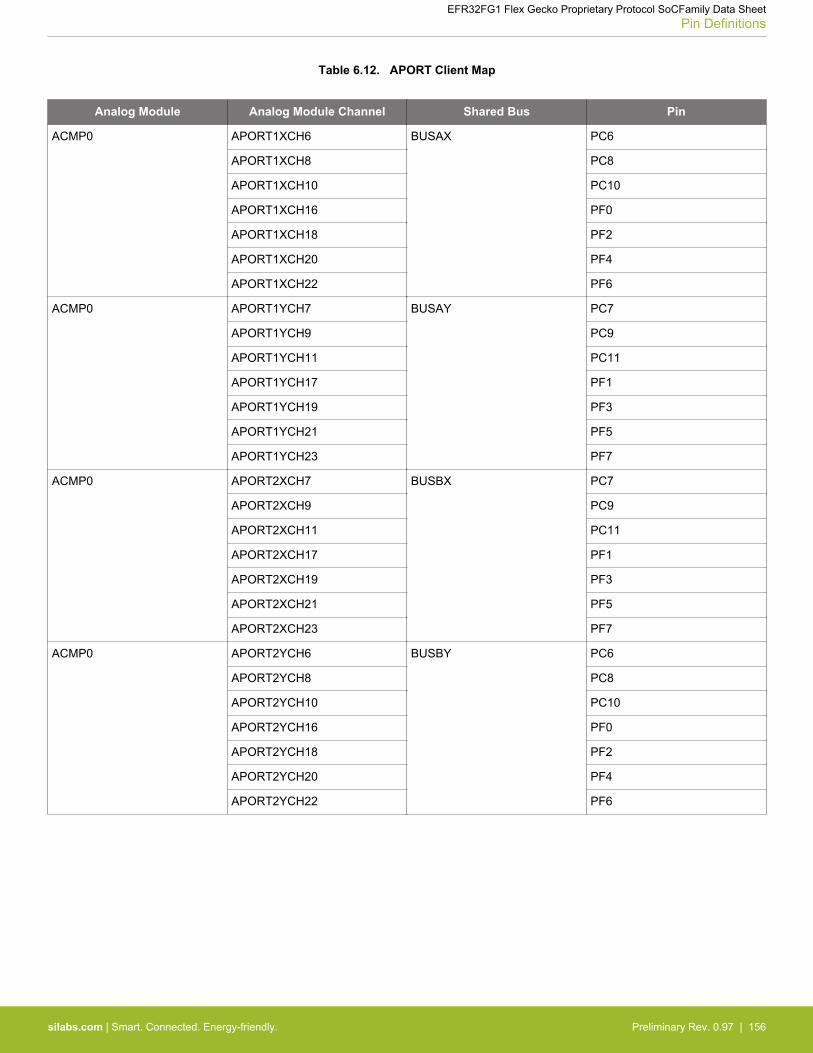
Table 6.12. APORT Client Map
Analog Module Analog Module Channel Shared Bus Pin
ACMP0 APORT1XCH6 BUSAX PC6
APORT1XCH8 PC8
APORT1XCH10 PC10
APORT1XCH16 PF0
APORT1XCH18 PF2
APORT1XCH20 PF4
APORT1XCH22 PF6
ACMP0 APORT1YCH7 BUSAY PC7
APORT1YCH9 PC9
APORT1YCH11 PC11
APORT1YCH17 PF1
APORT1YCH19 PF3
APORT1YCH21 PF5
APORT1YCH23 PF7
ACMP0 APORT2XCH7 BUSBX PC7
APORT2XCH9 PC9
APORT2XCH11 PC11
APORT2XCH17 PF1
APORT2XCH19 PF3
APORT2XCH21 PF5
APORT2XCH23 PF7
ACMP0 APORT2YCH6 BUSBY PC6
APORT2YCH8 PC8
APORT2YCH10 PC10
APORT2YCH16 PF0
APORT2YCH18 PF2
APORT2YCH20 PF4
APORT2YCH22 PF6
EFR32FG1 Flex Gecko Proprietary Protocol SoCFamily Data SheetPin Definitions
silabs.com | Smart. Connected. Energy-friendly. Preliminary Rev. 0.97 | 156
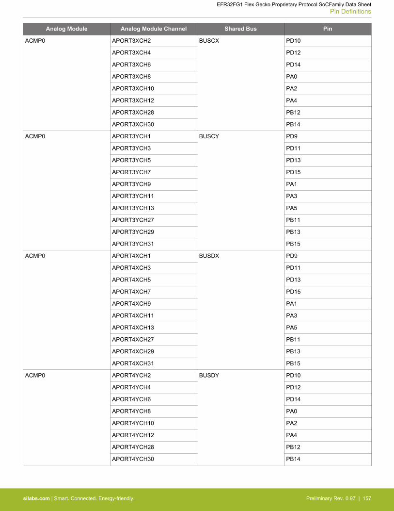
Analog Module Analog Module Channel Shared Bus Pin
ACMP0 APORT3XCH2 BUSCX PD10
APORT3XCH4 PD12
APORT3XCH6 PD14
APORT3XCH8 PA0
APORT3XCH10 PA2
APORT3XCH12 PA4
APORT3XCH28 PB12
APORT3XCH30 PB14
ACMP0 APORT3YCH1 BUSCY PD9
APORT3YCH3 PD11
APORT3YCH5 PD13
APORT3YCH7 PD15
APORT3YCH9 PA1
APORT3YCH11 PA3
APORT3YCH13 PA5
APORT3YCH27 PB11
APORT3YCH29 PB13
APORT3YCH31 PB15
ACMP0 APORT4XCH1 BUSDX PD9
APORT4XCH3 PD11
APORT4XCH5 PD13
APORT4XCH7 PD15
APORT4XCH9 PA1
APORT4XCH11 PA3
APORT4XCH13 PA5
APORT4XCH27 PB11
APORT4XCH29 PB13
APORT4XCH31 PB15
ACMP0 APORT4YCH2 BUSDY PD10
APORT4YCH4 PD12
APORT4YCH6 PD14
APORT4YCH8 PA0
APORT4YCH10 PA2
APORT4YCH12 PA4
APORT4YCH28 PB12
APORT4YCH30 PB14
EFR32FG1 Flex Gecko Proprietary Protocol SoCFamily Data SheetPin Definitions
silabs.com | Smart. Connected. Energy-friendly. Preliminary Rev. 0.97 | 157

Analog Module Analog Module Channel Shared Bus Pin
ACMP1 APORT1XCH6 BUSAX PC6
APORT1XCH8 PC8
APORT1XCH10 PC10
APORT1XCH16 PF0
APORT1XCH18 PF2
APORT1XCH20 PF4
APORT1XCH22 PF6
ACMP1 APORT1YCH7 BUSAY PC7
APORT1YCH9 PC9
APORT1YCH11 PC11
APORT1YCH17 PF1
APORT1YCH19 PF3
APORT1YCH21 PF5
APORT1YCH23 PF7
ACMP1 APORT2XCH7 BUSBX PC7
APORT2XCH9 PC9
APORT2XCH11 PC11
APORT2XCH17 PF1
APORT2XCH19 PF3
APORT2XCH21 PF5
APORT2XCH23 PF7
ACMP1 APORT2YCH6 BUSBY PC6
APORT2YCH8 PC8
APORT2YCH10 PC10
APORT2YCH16 PF0
APORT2YCH18 PF2
APORT2YCH20 PF4
APORT2YCH22 PF6
ACMP1 APORT3XCH2 BUSCX PD10
APORT3XCH4 PD12
APORT3XCH6 PD14
APORT3XCH8 PA0
APORT3XCH10 PA2
APORT3XCH12 PA4
APORT3XCH28 PB12
APORT3XCH30 PB14
EFR32FG1 Flex Gecko Proprietary Protocol SoCFamily Data SheetPin Definitions
silabs.com | Smart. Connected. Energy-friendly. Preliminary Rev. 0.97 | 158

Analog Module Analog Module Channel Shared Bus Pin
ACMP1 APORT3YCH1 BUSCY PD9
APORT3YCH3 PD11
APORT3YCH5 PD13
APORT3YCH7 PD15
APORT3YCH9 PA1
APORT3YCH11 PA3
APORT3YCH13 PA5
APORT3YCH27 PB11
APORT3YCH29 PB13
APORT3YCH31 PB15
ACMP1 APORT4XCH1 BUSDX PD9
APORT4XCH3 PD11
APORT4XCH5 PD13
APORT4XCH7 PD15
APORT4XCH9 PA1
APORT4XCH11 PA3
APORT4XCH13 PA5
APORT4XCH27 PB11
APORT4XCH29 PB13
APORT4XCH31 PB15
ACMP1 APORT4YCH2 BUSDY PD10
APORT4YCH4 PD12
APORT4YCH6 PD14
APORT4YCH8 PA0
APORT4YCH10 PA2
APORT4YCH12 PA4
APORT4YCH28 PB12
APORT4YCH30 PB14
ADC0 APORT1XCH6 BUSAX PC6
APORT1XCH8 PC8
APORT1XCH10 PC10
APORT1XCH16 PF0
APORT1XCH18 PF2
APORT1XCH20 PF4
APORT1XCH22 PF6
EFR32FG1 Flex Gecko Proprietary Protocol SoCFamily Data SheetPin Definitions
silabs.com | Smart. Connected. Energy-friendly. Preliminary Rev. 0.97 | 159
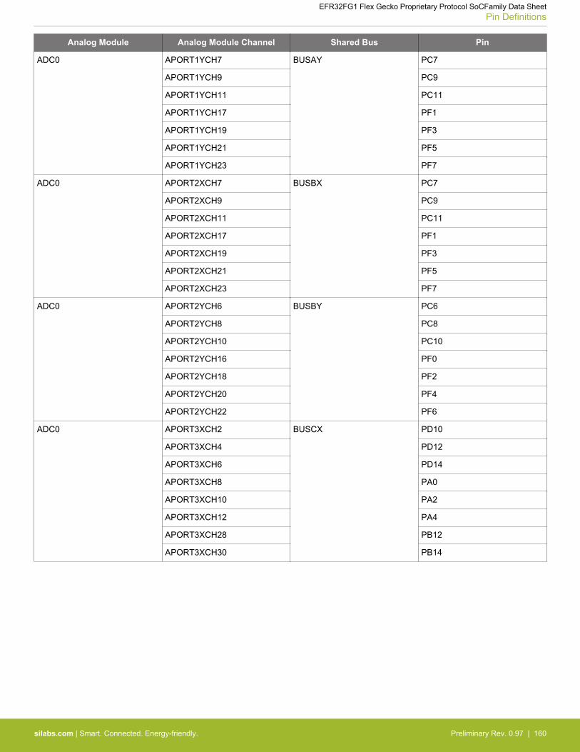
Analog Module Analog Module Channel Shared Bus Pin
ADC0 APORT1YCH7 BUSAY PC7
APORT1YCH9 PC9
APORT1YCH11 PC11
APORT1YCH17 PF1
APORT1YCH19 PF3
APORT1YCH21 PF5
APORT1YCH23 PF7
ADC0 APORT2XCH7 BUSBX PC7
APORT2XCH9 PC9
APORT2XCH11 PC11
APORT2XCH17 PF1
APORT2XCH19 PF3
APORT2XCH21 PF5
APORT2XCH23 PF7
ADC0 APORT2YCH6 BUSBY PC6
APORT2YCH8 PC8
APORT2YCH10 PC10
APORT2YCH16 PF0
APORT2YCH18 PF2
APORT2YCH20 PF4
APORT2YCH22 PF6
ADC0 APORT3XCH2 BUSCX PD10
APORT3XCH4 PD12
APORT3XCH6 PD14
APORT3XCH8 PA0
APORT3XCH10 PA2
APORT3XCH12 PA4
APORT3XCH28 PB12
APORT3XCH30 PB14
EFR32FG1 Flex Gecko Proprietary Protocol SoCFamily Data SheetPin Definitions
silabs.com | Smart. Connected. Energy-friendly. Preliminary Rev. 0.97 | 160

Analog Module Analog Module Channel Shared Bus Pin
ADC0 APORT3YCH1 BUSCY PD9
APORT3YCH3 PD11
APORT3YCH5 PD13
APORT3YCH7 PD15
APORT3YCH9 PA1
APORT3YCH11 PA3
APORT3YCH13 PA5
APORT3YCH27 PB11
APORT3YCH29 PB13
APORT3YCH31 PB15
ADC0 APORT4XCH1 BUSDX PD9
APORT4XCH3 PD11
APORT4XCH5 PD13
APORT4XCH7 PD15
APORT4XCH9 PA1
APORT4XCH11 PA3
APORT4XCH13 PA5
APORT4XCH27 PB11
APORT4XCH29 PB13
APORT4XCH31 PB15
ADC0 APORT4YCH2 BUSDY PD10
APORT4YCH4 PD12
APORT4YCH6 PD14
APORT4YCH8 PA0
APORT4YCH10 PA2
APORT4YCH12 PA4
APORT4YCH28 PB12
APORT4YCH30 PB14
IDAC0 APORT1XCH2 BUSCX PD10
APORT1XCH4 PD12
APORT1XCH6 PD14
APORT1XCH8 PA0
APORT1XCH10 PA2
APORT1XCH12 PA4
APORT1XCH28 PB12
APORT1XCH30 PB14
EFR32FG1 Flex Gecko Proprietary Protocol SoCFamily Data SheetPin Definitions
silabs.com | Smart. Connected. Energy-friendly. Preliminary Rev. 0.97 | 161
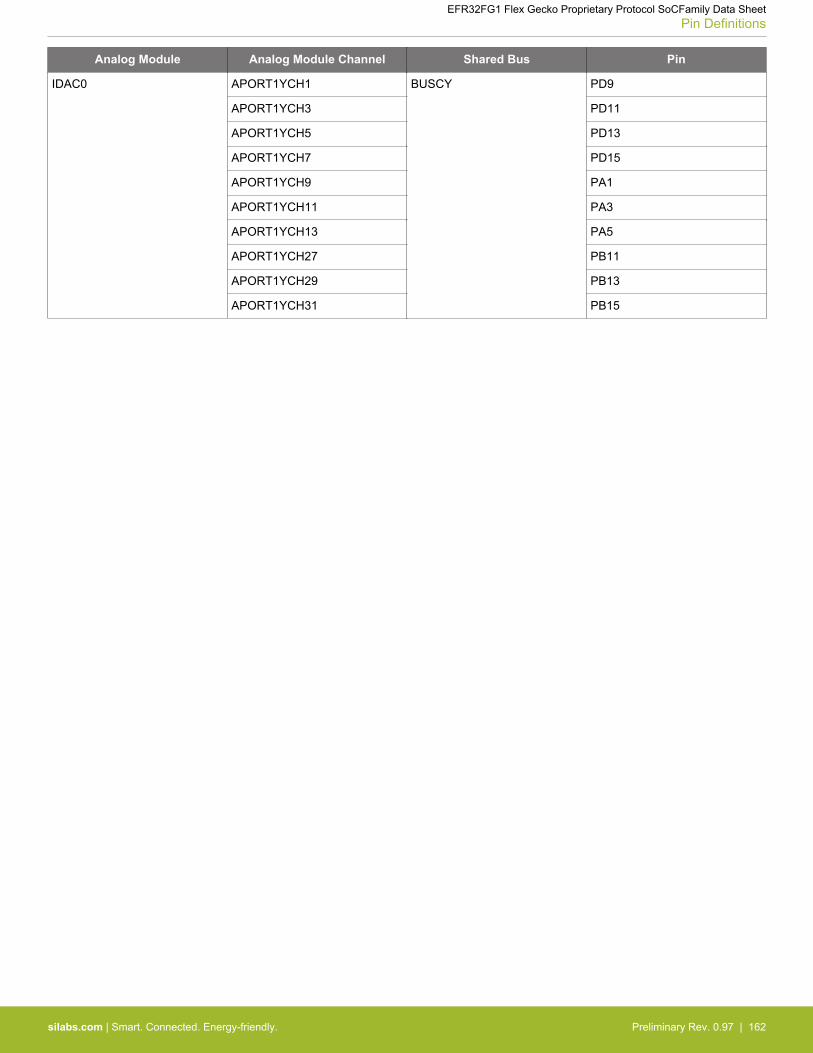
Analog Module Analog Module Channel Shared Bus Pin
IDAC0 APORT1YCH1 BUSCY PD9
APORT1YCH3 PD11
APORT1YCH5 PD13
APORT1YCH7 PD15
APORT1YCH9 PA1
APORT1YCH11 PA3
APORT1YCH13 PA5
APORT1YCH27 PB11
APORT1YCH29 PB13
APORT1YCH31 PB15
EFR32FG1 Flex Gecko Proprietary Protocol SoCFamily Data SheetPin Definitions
silabs.com | Smart. Connected. Energy-friendly. Preliminary Rev. 0.97 | 162
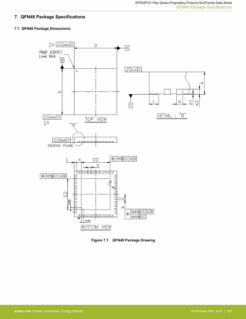
7. QFN48 Package Specifications
7.1 QFN48 Package Dimensions
Figure 7.1. QFN48 Package Drawing
EFR32FG1 Flex Gecko Proprietary Protocol SoCFamily Data SheetQFN48 Package Specifications
silabs.com | Smart. Connected. Energy-friendly. Preliminary Rev. 0.97 | 163
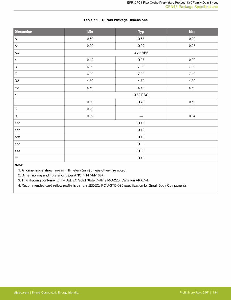
Table 7.1. QFN48 Package Dimensions
Dimension Min Typ Max
A 0.80 0.85 0.90
A1 0.00 0.02 0.05
A3 0.20 REF
b 0.18 0.25 0.30
D 6.90 7.00 7.10
E 6.90 7.00 7.10
D2 4.60 4.70 4.80
E2 4.60 4.70 4.80
e 0.50 BSC
L 0.30 0.40 0.50
K 0.20 — —
R 0.09 — 0.14
aaa 0.15
bbb 0.10
ccc 0.10
ddd 0.05
eee 0.08
fff 0.10
Note:1. All dimensions shown are in millimeters (mm) unless otherwise noted.2. Dimensioning and Tolerancing per ANSI Y14.5M-1994.3. This drawing conforms to the JEDEC Solid State Outline MO-220, Variation VKKD-4.4. Recommended card reflow profile is per the JEDEC/IPC J-STD-020 specification for Small Body Components.
EFR32FG1 Flex Gecko Proprietary Protocol SoCFamily Data SheetQFN48 Package Specifications
silabs.com | Smart. Connected. Energy-friendly. Preliminary Rev. 0.97 | 164
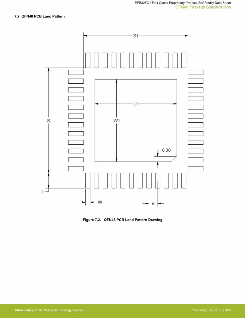
7.2 QFN48 PCB Land Pattern
Figure 7.2. QFN48 PCB Land Pattern Drawing
EFR32FG1 Flex Gecko Proprietary Protocol SoCFamily Data SheetQFN48 Package Specifications
silabs.com | Smart. Connected. Energy-friendly. Preliminary Rev. 0.97 | 165
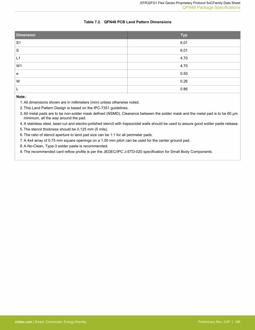
Table 7.2. QFN48 PCB Land Pattern Dimensions
Dimension Typ
S1 6.01
S 6.01
L1 4.70
W1 4.70
e 0.50
W 0.26
L 0.86
Note:1. All dimensions shown are in millimeters (mm) unless otherwise noted.2. This Land Pattern Design is based on the IPC-7351 guidelines.3. All metal pads are to be non-solder mask defined (NSMD). Clearance between the solder mask and the metal pad is to be 60 µm
minimum, all the way around the pad.4. A stainless steel, laser-cut and electro-polished stencil with trapezoidal walls should be used to assure good solder paste release.5. The stencil thickness should be 0.125 mm (5 mils).6. The ratio of stencil aperture to land pad size can be 1:1 for all perimeter pads.7. A 4x4 array of 0.75 mm square openings on a 1.00 mm pitch can be used for the center ground pad.8. A No-Clean, Type-3 solder paste is recommended.9. The recommended card reflow profile is per the JEDEC/IPC J-STD-020 specification for Small Body Components.
EFR32FG1 Flex Gecko Proprietary Protocol SoCFamily Data SheetQFN48 Package Specifications
silabs.com | Smart. Connected. Energy-friendly. Preliminary Rev. 0.97 | 166
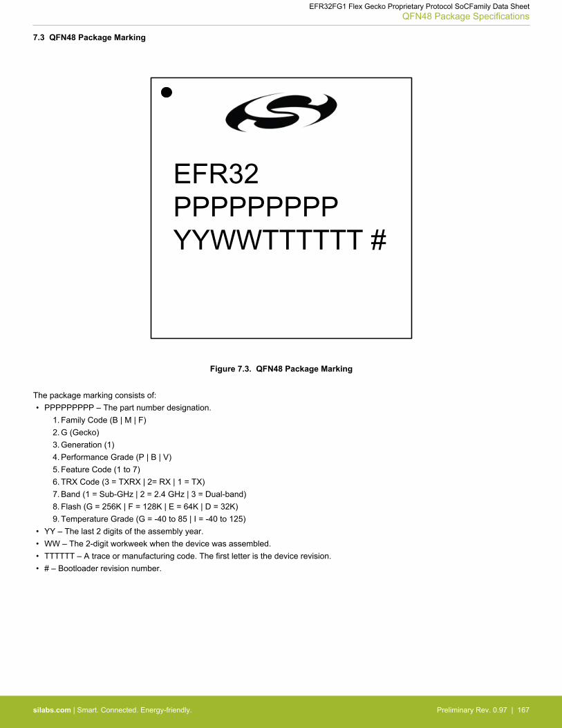
7.3 QFN48 Package Marking
EFR32PPPPPPPPPYYWWTTTTTT #
Figure 7.3. QFN48 Package Marking
The package marking consists of:• PPPPPPPPP – The part number designation.
1. Family Code (B | M | F)2. G (Gecko)3. Generation (1)4. Performance Grade (P | B | V)5. Feature Code (1 to 7)6. TRX Code (3 = TXRX | 2= RX | 1 = TX)7. Band (1 = Sub-GHz | 2 = 2.4 GHz | 3 = Dual-band)8. Flash (G = 256K | F = 128K | E = 64K | D = 32K)9. Temperature Grade (G = -40 to 85 | I = -40 to 125)
• YY – The last 2 digits of the assembly year.• WW – The 2-digit workweek when the device was assembled.• TTTTTT – A trace or manufacturing code. The first letter is the device revision.• # – Bootloader revision number.
EFR32FG1 Flex Gecko Proprietary Protocol SoCFamily Data SheetQFN48 Package Specifications
silabs.com | Smart. Connected. Energy-friendly. Preliminary Rev. 0.97 | 167
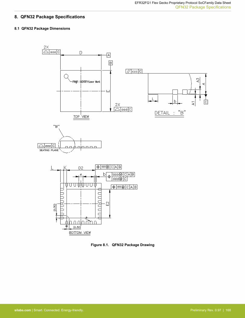
8. QFN32 Package Specifications
8.1 QFN32 Package Dimensions
Figure 8.1. QFN32 Package Drawing
EFR32FG1 Flex Gecko Proprietary Protocol SoCFamily Data SheetQFN32 Package Specifications
silabs.com | Smart. Connected. Energy-friendly. Preliminary Rev. 0.97 | 168
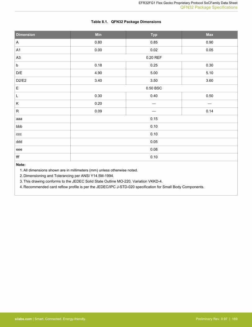
Table 8.1. QFN32 Package Dimensions
Dimension Min Typ Max
A 0.80 0.85 0.90
A1 0.00 0.02 0.05
A3 0.20 REF
b 0.18 0.25 0.30
D/E 4.90 5.00 5.10
D2/E2 3.40 3.50 3.60
E 0.50 BSC
L 0.30 0.40 0.50
K 0.20 — —
R 0.09 — 0.14
aaa 0.15
bbb 0.10
ccc 0.10
ddd 0.05
eee 0.08
fff 0.10
Note:1. All dimensions shown are in millimeters (mm) unless otherwise noted.2. Dimensioning and Tolerancing per ANSI Y14.5M-1994.3. This drawing conforms to the JEDEC Solid State Outline MO-220, Variation VKKD-4.4. Recommended card reflow profile is per the JEDEC/IPC J-STD-020 specification for Small Body Components.
EFR32FG1 Flex Gecko Proprietary Protocol SoCFamily Data SheetQFN32 Package Specifications
silabs.com | Smart. Connected. Energy-friendly. Preliminary Rev. 0.97 | 169
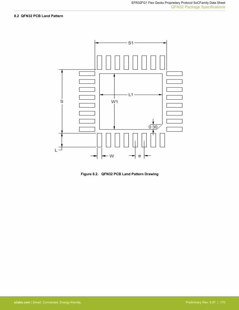
8.2 QFN32 PCB Land Pattern
Figure 8.2. QFN32 PCB Land Pattern Drawing
EFR32FG1 Flex Gecko Proprietary Protocol SoCFamily Data SheetQFN32 Package Specifications
silabs.com | Smart. Connected. Energy-friendly. Preliminary Rev. 0.97 | 170
Table 8.2. QFN32 PCB Land Pattern Dimensions
Dimension Typ
S1 4.01
S 4.01
L1 3.50
W1 3.50
e 0.50
W 0.26
L 0.86
Note:1. All dimensions shown are in millimeters (mm) unless otherwise noted.2. This Land Pattern Design is based on the IPC-7351 guidelines.3. All metal pads are to be non-solder mask defined (NSMD). Clearance between the solder mask and the metal pad is to be 60 µm
minimum, all the way around the pad.4. A stainless steel, laser-cut and electro-polished stencil with trapezoidal walls should be used to assure good solder paste release.5. The stencil thickness should be 0.125 mm (5 mils).6. The ratio of stencil aperture to land pad size can be 1:1 for all perimeter pads.7. A 3x3 array of 0.85 mm square openings on a 1.00 mm pitch can be used for the center ground pad.8. A No-Clean, Type-3 solder paste is recommended.9. The recommended card reflow profile is per the JEDEC/IPC J-STD-020 specification for Small Body Components.
EFR32FG1 Flex Gecko Proprietary Protocol SoCFamily Data SheetQFN32 Package Specifications
silabs.com | Smart. Connected. Energy-friendly. Preliminary Rev. 0.97 | 171
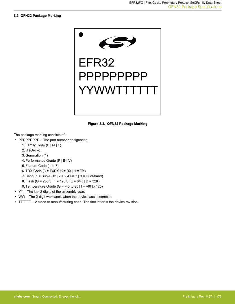
8.3 QFN32 Package Marking
EFR32PPPPPPPPPYYWWTTTTTT
Figure 8.3. QFN32 Package Marking
The package marking consists of:• PPPPPPPPP – The part number designation.
1. Family Code (B | M | F)2. G (Gecko)3. Generation (1)4. Performance Grade (P | B | V)5. Feature Code (1 to 7)6. TRX Code (3 = TXRX | 2= RX | 1 = TX)7. Band (1 = Sub-GHz | 2 = 2.4 GHz | 3 = Dual-band)8. Flash (G = 256K | F = 128K | E = 64K | D = 32K)9. Temperature Grade (G = -40 to 85 | I = -40 to 125)
• YY – The last 2 digits of the assembly year.• WW – The 2-digit workweek when the device was assembled.• TTTTTT – A trace or manufacturing code. The first letter is the device revision.
EFR32FG1 Flex Gecko Proprietary Protocol SoCFamily Data SheetQFN32 Package Specifications
silabs.com | Smart. Connected. Energy-friendly. Preliminary Rev. 0.97 | 172
9. Revision History
9.1 Revision 0.97
2016-06-06
• Added dual-band and sub-GHz OPNs.
9.2 Revision 0.951
2016-06-03
• Electrical specification tables updated with additional characterization data.
9.3 Revision 0.95
2016-04-11
• All OPNs changed to rev C0. Note the following:• All OPNs ending in -B0 are Engineering Samples based on an older revision of silicon and are being removed from the OPN
table. These older revisions should be used for evaluation only and will not be supported for production.• OPNs ending in -C0 are the Current Revision of Silicon and are intended for production.
• Electrical specification tables updated with latest characterization data and production test limits.
9.4 Revision 0.9
2016-01-12
• Updated electrical specifications with latest characterization data.• Added thermal characteristics table.• Updated OPN decoder figure to include extended family options.
9.5 Revision 0.81
2015-12-01
• Engineering samples note added to ordering information table.
9.6 Revision 0.8
2015-11-14
• Initial external release.• Consolidated individual device datasheets into single-family document.• Re-formatted ordering information table and OPN decoder.• Updated block diagrams for front page and system overview.• Removed extraneous sections from DC-DC and wake-on-radio from system overview.• Updated table formatting for electrical specifications to tech pubs standards.• Updated electrcal specifications with latest available data.• Added I2C and USART SPI timing tables.• Moved DC-DC graph to typical performance curves.• Updated APORT tables and APORT references to correct nomenclature.
EFR32FG1 Flex Gecko Proprietary Protocol SoCFamily Data SheetRevision History
silabs.com | Smart. Connected. Energy-friendly. Preliminary Rev. 0.97 | 173
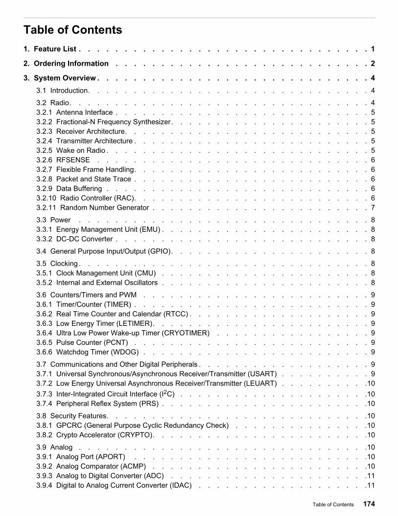
Table of Contents1. Feature List . . . . . . . . . . . . . . . . . . . . . . . . . . . . . . . . 1
2. Ordering Information . . . . . . . . . . . . . . . . . . . . . . . . . . . . 2
3. System Overview . . . . . . . . . . . . . . . . . . . . . . . . . . . . . . 43.1 Introduction. . . . . . . . . . . . . . . . . . . . . . . . . . . . . . . 4
3.2 Radio. . . . . . . . . . . . . . . . . . . . . . . . . . . . . . . . . 43.2.1 Antenna Interface . . . . . . . . . . . . . . . . . . . . . . . . . . . . 53.2.2 Fractional-N Frequency Synthesizer. . . . . . . . . . . . . . . . . . . . . . 53.2.3 Receiver Architecture. . . . . . . . . . . . . . . . . . . . . . . . . . . 53.2.4 Transmitter Architecture . . . . . . . . . . . . . . . . . . . . . . . . . . 53.2.5 Wake on Radio . . . . . . . . . . . . . . . . . . . . . . . . . . . . . 53.2.6 RFSENSE . . . . . . . . . . . . . . . . . . . . . . . . . . . . . . 63.2.7 Flexible Frame Handling. . . . . . . . . . . . . . . . . . . . . . . . . . 63.2.8 Packet and State Trace . . . . . . . . . . . . . . . . . . . . . . . . . . 63.2.9 Data Buffering . . . . . . . . . . . . . . . . . . . . . . . . . . . . . 63.2.10 Radio Controller (RAC). . . . . . . . . . . . . . . . . . . . . . . . . . 63.2.11 Random Number Generator . . . . . . . . . . . . . . . . . . . . . . . . 7
3.3 Power . . . . . . . . . . . . . . . . . . . . . . . . . . . . . . . . 83.3.1 Energy Management Unit (EMU) . . . . . . . . . . . . . . . . . . . . . . . 83.3.2 DC-DC Converter . . . . . . . . . . . . . . . . . . . . . . . . . . . . 8
3.4 General Purpose Input/Output (GPIO). . . . . . . . . . . . . . . . . . . . . . 8
3.5 Clocking . . . . . . . . . . . . . . . . . . . . . . . . . . . . . . . . 83.5.1 Clock Management Unit (CMU) . . . . . . . . . . . . . . . . . . . . . . . 83.5.2 Internal and External Oscillators . . . . . . . . . . . . . . . . . . . . . . . 8
3.6 Counters/Timers and PWM . . . . . . . . . . . . . . . . . . . . . . . . . 93.6.1 Timer/Counter (TIMER) . . . . . . . . . . . . . . . . . . . . . . . . . . 93.6.2 Real Time Counter and Calendar (RTCC) . . . . . . . . . . . . . . . . . . . . 93.6.3 Low Energy Timer (LETIMER). . . . . . . . . . . . . . . . . . . . . . . . 93.6.4 Ultra Low Power Wake-up Timer (CRYOTIMER) . . . . . . . . . . . . . . . . . 93.6.5 Pulse Counter (PCNT) . . . . . . . . . . . . . . . . . . . . . . . . . . 93.6.6 Watchdog Timer (WDOG) . . . . . . . . . . . . . . . . . . . . . . . . . 9
3.7 Communications and Other Digital Peripherals . . . . . . . . . . . . . . . . . . . 93.7.1 Universal Synchronous/Asynchronous Receiver/Transmitter (USART) . . . . . . . . . . 93.7.2 Low Energy Universal Asynchronous Receiver/Transmitter (LEUART) . . . . . . . . . .103.7.3 Inter-Integrated Circuit Interface (I2C) . . . . . . . . . . . . . . . . . . . . .103.7.4 Peripheral Reflex System (PRS) . . . . . . . . . . . . . . . . . . . . . . .10
3.8 Security Features. . . . . . . . . . . . . . . . . . . . . . . . . . . . .103.8.1 GPCRC (General Purpose Cyclic Redundancy Check) . . . . . . . . . . . . . . .103.8.2 Crypto Accelerator (CRYPTO). . . . . . . . . . . . . . . . . . . . . . . .10
3.9 Analog . . . . . . . . . . . . . . . . . . . . . . . . . . . . . . . .103.9.1 Analog Port (APORT) . . . . . . . . . . . . . . . . . . . . . . . . . .103.9.2 Analog Comparator (ACMP) . . . . . . . . . . . . . . . . . . . . . . . .103.9.3 Analog to Digital Converter (ADC) . . . . . . . . . . . . . . . . . . . . . .113.9.4 Digital to Analog Current Converter (IDAC) . . . . . . . . . . . . . . . . . . .11
Table of Contents 174
3.10 Reset Management Unit (RMU) . . . . . . . . . . . . . . . . . . . . . . .11
3.11 Core and Memory . . . . . . . . . . . . . . . . . . . . . . . . . . . .113.11.1 Processor Core . . . . . . . . . . . . . . . . . . . . . . . . . . . .113.11.2 Memory System Controller (MSC) . . . . . . . . . . . . . . . . . . . . . .113.11.3 Linked Direct Memory Access Controller (LDMA) . . . . . . . . . . . . . . . . .11
3.12 Memory Map . . . . . . . . . . . . . . . . . . . . . . . . . . . . . .12
3.13 Configuration Summary . . . . . . . . . . . . . . . . . . . . . . . . . .13
4. Electrical Specifications . . . . . . . . . . . . . . . . . . . . . . . . . . 144.1 Electrical Characteristics . . . . . . . . . . . . . . . . . . . . . . . . . .144.1.1 Absolute Maximum Ratings . . . . . . . . . . . . . . . . . . . . . . . .154.1.2 Operating Conditions . . . . . . . . . . . . . . . . . . . . . . . . . . .174.1.2.1 General Operating Conditions . . . . . . . . . . . . . . . . . . . . . . .174.1.3 Thermal Characteristics . . . . . . . . . . . . . . . . . . . . . . . . . .184.1.4 DC-DC Converter . . . . . . . . . . . . . . . . . . . . . . . . . . . .194.1.5 Current Consumption. . . . . . . . . . . . . . . . . . . . . . . . . . .214.1.5.1 Current Consumption 3.3 V without DC-DC Converter . . . . . . . . . . . . . . .214.1.5.2 Current Consumption 3.3 V using DC-DC Converter . . . . . . . . . . . . . . .224.1.5.3 Current Consumption 1.85 V without DC-DC Converter . . . . . . . . . . . . . .244.1.5.4 Current Consumption Using Radio . . . . . . . . . . . . . . . . . . . . .254.1.6 Wake up times . . . . . . . . . . . . . . . . . . . . . . . . . . . . .274.1.7 Brown Out Detector . . . . . . . . . . . . . . . . . . . . . . . . . . .274.1.8 Frequency Synthesizer Characteristics . . . . . . . . . . . . . . . . . . . . .284.1.9 2.4 GHz RF Transceiver Characteristics . . . . . . . . . . . . . . . . . . . .294.1.9.1 RF Transmitter General Characteristics for the 2.4 GHz Band . . . . . . . . . . . .294.1.9.2 RF Receiver General Characteristics for the 2.4 GHz Band . . . . . . . . . . . . .304.1.9.3 RF Transmitter Characteristics for 1Mbps 2GFSK in the 2.4 GHz Band . . . . . . . . .314.1.9.4 RF Receiver Characteristics for 1Mbps 2GFSK in the 2.4 GHz Band . . . . . . . . . .324.1.9.5 RF Transmitter Characteristics for 802.15.4 O-QPSK DSSS in the 2.4 GHz Band . . . . . .344.1.9.6 RF Receiver Characteristics for 802.15.4 O-QPSK DSSS in the 2.4 GHz Band. . . . . . .364.1.10 Sub-GHz RF Transceiver Characteristics . . . . . . . . . . . . . . . . . . .384.1.10.1 Sub-GHz RF Transmitter Characteristics in the 915 MHz Band . . . . . . . . . . .394.1.10.2 Sub-GHz RF Receiver Characteristics in the 915 MHz Band . . . . . . . . . . . .424.1.10.3 Sub-GHz RF Transmitter Characteristics in the 868 MHz Band . . . . . . . . . . .454.1.10.4 Sub-GHz RF Receiver Characteristics in the 868 MHz Band . . . . . . . . . . . .464.1.10.5 Sub-GHz RF Transmitter Characteristics in the 490 MHz Band . . . . . . . . . . .484.1.10.6 Sub-GHz RF Receiver Characteristics in the 490 MHz Band . . . . . . . . . . . .494.1.10.7 Sub-GHz RF Transmitter Characteristics in the 433 MHz Band . . . . . . . . . . .514.1.10.8 Sub-GHz RF Receiver Characteristics in the 433 MHz Band . . . . . . . . . . . .544.1.10.9 Sub-GHz RF Transmitter Characteristics in the 315 MHz Band . . . . . . . . . . .574.1.10.10 Sub-GHz RF Receiver Characteristics in the 315 MHz Band . . . . . . . . . . . .594.1.10.11 Sub-GHz RF Transmitter Characteristics in the 169 MHz Band . . . . . . . . . . .614.1.10.12 Sub-GHz RF Receiver Characteristics in the 169 MHz Band . . . . . . . . . . . .624.1.11 Modem Features . . . . . . . . . . . . . . . . . . . . . . . . . . . .634.1.12 Oscillators . . . . . . . . . . . . . . . . . . . . . . . . . . . . . .644.1.12.1 LFXO . . . . . . . . . . . . . . . . . . . . . . . . . . . . . . .644.1.12.2 HFXO . . . . . . . . . . . . . . . . . . . . . . . . . . . . . . .654.1.12.3 LFRCO . . . . . . . . . . . . . . . . . . . . . . . . . . . . . .654.1.12.4 HFRCO and AUXHFRCO . . . . . . . . . . . . . . . . . . . . . . . .664.1.12.5 ULFRCO . . . . . . . . . . . . . . . . . . . . . . . . . . . . . .664.1.13 Flash Memory Characteristics . . . . . . . . . . . . . . . . . . . . . . .67
Table of Contents 175
4.1.14 GPIO. . . . . . . . . . . . . . . . . . . . . . . . . . . . . . . .684.1.15 VMON . . . . . . . . . . . . . . . . . . . . . . . . . . . . . . .694.1.16 ADC . . . . . . . . . . . . . . . . . . . . . . . . . . . . . . . .704.1.17 IDAC . . . . . . . . . . . . . . . . . . . . . . . . . . . . . . . .724.1.18 Analog Comparator (ACMP) . . . . . . . . . . . . . . . . . . . . . . . .744.1.19 I2C . . . . . . . . . . . . . . . . . . . . . . . . . . . . . . . .764.1.20 USART SPI . . . . . . . . . . . . . . . . . . . . . . . . . . . . .78
4.2 Typical Performance Curves . . . . . . . . . . . . . . . . . . . . . . . . .794.2.1 Supply Current . . . . . . . . . . . . . . . . . . . . . . . . . . . . .804.2.2 DC-DC Converter . . . . . . . . . . . . . . . . . . . . . . . . . . . .824.2.3 Internal Oscillators. . . . . . . . . . . . . . . . . . . . . . . . . . . .844.2.4 2.4 GHz Radio . . . . . . . . . . . . . . . . . . . . . . . . . . . . .90
5. Typical Connection Diagrams . . . . . . . . . . . . . . . . . . . . . . . . 925.1 Power . . . . . . . . . . . . . . . . . . . . . . . . . . . . . . . .92
5.2 RF Matching Networks . . . . . . . . . . . . . . . . . . . . . . . . . . .94
5.3 Other Connections . . . . . . . . . . . . . . . . . . . . . . . . . . . .95
6. Pin Definitions . . . . . . . . . . . . . . . . . . . . . . . . . . . . . . 966.1 EFR32FG1 QFN48 Sub-GHz Definition . . . . . . . . . . . . . . . . . . . . .966.1.1 EFR32FG1 QFN48 Sub-GHz GPIO Overview . . . . . . . . . . . . . . . . . 108
6.2 EFR32FG1 QFN48 2.4 GHz Definition . . . . . . . . . . . . . . . . . . . . 1096.2.1 EFR32FG1 QFN48 2.4 GHz GPIO Overview . . . . . . . . . . . . . . . . . . 121
6.3 EFR32FG1 QFN48 2.4 GHz and Sub-GHz Definition. . . . . . . . . . . . . . . . 1226.3.1 EFR32FG1 QFN48 2.4 GHz and Sub-GHz GPIO Overview . . . . . . . . . . . . . 133
6.4 EFR32FG1 QFN32 Sub-GHz Definition . . . . . . . . . . . . . . . . . . . . 1346.4.1 EFR32FG1 QFN32 Sub-GHz GPIO Overview . . . . . . . . . . . . . . . . . 140
6.5 EFR32FG1 QFN32 2.4 GHz Definition . . . . . . . . . . . . . . . . . . . . 1416.5.1 EFR32FG1 QFN32 2.4 GHz GPIO Overview . . . . . . . . . . . . . . . . . . 147
6.6 Alternate Functionality Pinout . . . . . . . . . . . . . . . . . . . . . . . 148
6.7 Analog Port (APORT) . . . . . . . . . . . . . . . . . . . . . . . . . . 155
7. QFN48 Package Specifications. . . . . . . . . . . . . . . . . . . . . . . . 1637.1 QFN48 Package Dimensions. . . . . . . . . . . . . . . . . . . . . . . . 163
7.2 QFN48 PCB Land Pattern . . . . . . . . . . . . . . . . . . . . . . . . . 165
7.3 QFN48 Package Marking . . . . . . . . . . . . . . . . . . . . . . . . . 167
8. QFN32 Package Specifications. . . . . . . . . . . . . . . . . . . . . . . . 1688.1 QFN32 Package Dimensions. . . . . . . . . . . . . . . . . . . . . . . . 168
8.2 QFN32 PCB Land Pattern . . . . . . . . . . . . . . . . . . . . . . . . . 170
8.3 QFN32 Package Marking . . . . . . . . . . . . . . . . . . . . . . . . . 172
9. Revision History . . . . . . . . . . . . . . . . . . . . . . . . . . . . . 1739.1 Revision 0.97 . . . . . . . . . . . . . . . . . . . . . . . . . . . . . 173
9.2 Revision 0.951 . . . . . . . . . . . . . . . . . . . . . . . . . . . . 173
Table of Contents 176
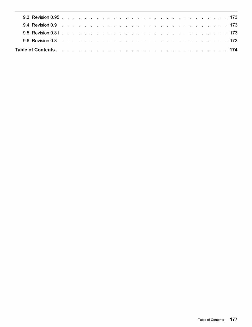
9.3 Revision 0.95 . . . . . . . . . . . . . . . . . . . . . . . . . . . . . 173
9.4 Revision 0.9 . . . . . . . . . . . . . . . . . . . . . . . . . . . . . 173
9.5 Revision 0.81 . . . . . . . . . . . . . . . . . . . . . . . . . . . . . 173
9.6 Revision 0.8 . . . . . . . . . . . . . . . . . . . . . . . . . . . . . 173
Table of Contents . . . . . . . . . . . . . . . . . . . . . . . . . . . . . . 174
Table of Contents 177

http://www.silabs.com
Silicon Laboratories Inc.400 West Cesar ChavezAustin, TX 78701USA
Simplicity StudioOne-click access to MCU and wireless tools, documentation, software, source code libraries & more. Available for Windows, Mac and Linux!
IoT Portfoliowww.silabs.com/IoT
SW/HWwww.silabs.com/simplicity
Qualitywww.silabs.com/quality
Support and Communitycommunity.silabs.com
DisclaimerSilicon Laboratories intends to provide customers with the latest, accurate, and in-depth documentation of all peripherals and modules available for system and software implementers using or intending to use the Silicon Laboratories products. Characterization data, available modules and peripherals, memory sizes and memory addresses refer to each specific device, and "Typical" parameters provided can and do vary in different applications. Application examples described herein are for illustrative purposes only. Silicon Laboratories reserves the right to make changes without further notice and limitation to product information, specifications, and descriptions herein, and does not give warranties as to the accuracy or completeness of the included information. Silicon Laboratories shall have no liability for the consequences of use of the information supplied herein. This document does not imply or express copyright licenses granted hereunder to design or fabricate any integrated circuits. The products are not designed or authorized to be used within any Life Support System without the specific written consent of Silicon Laboratories. A "Life Support System" is any product or system intended to support or sustain life and/or health, which, if it fails, can be reasonably expected to result in significant personal injury or death. Silicon Laboratories products are not designed or authorized for military applications. Silicon Laboratories products shall under no circumstances be used in weapons of mass destruction including (but not limited to) nuclear, biological or chemical weapons, or missiles capable of delivering such weapons.
Trademark InformationSilicon Laboratories Inc.® , Silicon Laboratories®, Silicon Labs®, SiLabs® and the Silicon Labs logo®, Bluegiga®, Bluegiga Logo®, Clockbuilder®, CMEMS®, DSPLL®, EFM®, EFM32®, EFR, Ember®, Energy Micro, Energy Micro logo and combinations thereof, "the world’s most energy friendly microcontrollers", Ember®, EZLink®, EZRadio®, EZRadioPRO®, Gecko®, ISOmodem®, Precision32®, ProSLIC®, Simplicity Studio®, SiPHY®, Telegesis, the Telegesis Logo®, USBXpress® and others are trademarks or registered trademarks of Silicon Laborato-ries Inc. ARM, CORTEX, Cortex-M3 and THUMB are trademarks or registered trademarks of ARM Holdings. Keil is a registered trademark of ARM Limited. All other products or brand names mentioned herein are trademarks of their respective holders.